WO2019239889A1 - 液晶パネル製造方法 - Google Patents
液晶パネル製造方法 Download PDFInfo
- Publication number
- WO2019239889A1 WO2019239889A1 PCT/JP2019/021217 JP2019021217W WO2019239889A1 WO 2019239889 A1 WO2019239889 A1 WO 2019239889A1 JP 2019021217 W JP2019021217 W JP 2019021217W WO 2019239889 A1 WO2019239889 A1 WO 2019239889A1
- Authority
- WO
- WIPO (PCT)
- Prior art keywords
- liquid crystal
- etching
- crystal panel
- base material
- line
- Prior art date
- Legal status (The legal status is an assumption and is not a legal conclusion. Google has not performed a legal analysis and makes no representation as to the accuracy of the status listed.)
- Ceased
Links
Images



Classifications
-
- C—CHEMISTRY; METALLURGY
- C03—GLASS; MINERAL OR SLAG WOOL
- C03B—MANUFACTURE, SHAPING, OR SUPPLEMENTARY PROCESSES
- C03B33/00—Severing cooled glass
- C03B33/07—Cutting armoured, multi-layered, coated or laminated, glass products
-
- C—CHEMISTRY; METALLURGY
- C03—GLASS; MINERAL OR SLAG WOOL
- C03C—CHEMICAL COMPOSITION OF GLASSES, GLAZES OR VITREOUS ENAMELS; SURFACE TREATMENT OF GLASS; SURFACE TREATMENT OF FIBRES OR FILAMENTS MADE FROM GLASS, MINERALS OR SLAGS; JOINING GLASS TO GLASS OR OTHER MATERIALS
- C03C15/00—Surface treatment of glass, not in the form of fibres or filaments, by etching
-
- C—CHEMISTRY; METALLURGY
- C03—GLASS; MINERAL OR SLAG WOOL
- C03C—CHEMICAL COMPOSITION OF GLASSES, GLAZES OR VITREOUS ENAMELS; SURFACE TREATMENT OF GLASS; SURFACE TREATMENT OF FIBRES OR FILAMENTS MADE FROM GLASS, MINERALS OR SLAGS; JOINING GLASS TO GLASS OR OTHER MATERIALS
- C03C23/00—Other surface treatment of glass not in the form of fibres or filaments
-
- G—PHYSICS
- G02—OPTICS
- G02F—OPTICAL DEVICES OR ARRANGEMENTS FOR THE CONTROL OF LIGHT BY MODIFICATION OF THE OPTICAL PROPERTIES OF THE MEDIA OF THE ELEMENTS INVOLVED THEREIN; NON-LINEAR OPTICS; FREQUENCY-CHANGING OF LIGHT; OPTICAL LOGIC ELEMENTS; OPTICAL ANALOGUE/DIGITAL CONVERTERS
- G02F1/00—Devices or arrangements for the control of the intensity, colour, phase, polarisation or direction of light arriving from an independent light source, e.g. switching, gating or modulating; Non-linear optics
- G02F1/01—Devices or arrangements for the control of the intensity, colour, phase, polarisation or direction of light arriving from an independent light source, e.g. switching, gating or modulating; Non-linear optics for the control of the intensity, phase, polarisation or colour
- G02F1/13—Devices or arrangements for the control of the intensity, colour, phase, polarisation or direction of light arriving from an independent light source, e.g. switching, gating or modulating; Non-linear optics for the control of the intensity, phase, polarisation or colour based on liquid crystals, e.g. single liquid crystal display cells
-
- G—PHYSICS
- G02—OPTICS
- G02F—OPTICAL DEVICES OR ARRANGEMENTS FOR THE CONTROL OF LIGHT BY MODIFICATION OF THE OPTICAL PROPERTIES OF THE MEDIA OF THE ELEMENTS INVOLVED THEREIN; NON-LINEAR OPTICS; FREQUENCY-CHANGING OF LIGHT; OPTICAL LOGIC ELEMENTS; OPTICAL ANALOGUE/DIGITAL CONVERTERS
- G02F1/00—Devices or arrangements for the control of the intensity, colour, phase, polarisation or direction of light arriving from an independent light source, e.g. switching, gating or modulating; Non-linear optics
- G02F1/01—Devices or arrangements for the control of the intensity, colour, phase, polarisation or direction of light arriving from an independent light source, e.g. switching, gating or modulating; Non-linear optics for the control of the intensity, phase, polarisation or colour
- G02F1/13—Devices or arrangements for the control of the intensity, colour, phase, polarisation or direction of light arriving from an independent light source, e.g. switching, gating or modulating; Non-linear optics for the control of the intensity, phase, polarisation or colour based on liquid crystals, e.g. single liquid crystal display cells
- G02F1/133—Constructional arrangements; Operation of liquid crystal cells; Circuit arrangements
- G02F1/1333—Constructional arrangements; Manufacturing methods
-
- G—PHYSICS
- G02—OPTICS
- G02F—OPTICAL DEVICES OR ARRANGEMENTS FOR THE CONTROL OF LIGHT BY MODIFICATION OF THE OPTICAL PROPERTIES OF THE MEDIA OF THE ELEMENTS INVOLVED THEREIN; NON-LINEAR OPTICS; FREQUENCY-CHANGING OF LIGHT; OPTICAL LOGIC ELEMENTS; OPTICAL ANALOGUE/DIGITAL CONVERTERS
- G02F1/00—Devices or arrangements for the control of the intensity, colour, phase, polarisation or direction of light arriving from an independent light source, e.g. switching, gating or modulating; Non-linear optics
- G02F1/01—Devices or arrangements for the control of the intensity, colour, phase, polarisation or direction of light arriving from an independent light source, e.g. switching, gating or modulating; Non-linear optics for the control of the intensity, phase, polarisation or colour
- G02F1/13—Devices or arrangements for the control of the intensity, colour, phase, polarisation or direction of light arriving from an independent light source, e.g. switching, gating or modulating; Non-linear optics for the control of the intensity, phase, polarisation or colour based on liquid crystals, e.g. single liquid crystal display cells
- G02F1/133—Constructional arrangements; Operation of liquid crystal cells; Circuit arrangements
- G02F1/1333—Constructional arrangements; Manufacturing methods
- G02F1/1345—Conductors connecting electrodes to cell terminals
-
- G—PHYSICS
- G02—OPTICS
- G02F—OPTICAL DEVICES OR ARRANGEMENTS FOR THE CONTROL OF LIGHT BY MODIFICATION OF THE OPTICAL PROPERTIES OF THE MEDIA OF THE ELEMENTS INVOLVED THEREIN; NON-LINEAR OPTICS; FREQUENCY-CHANGING OF LIGHT; OPTICAL LOGIC ELEMENTS; OPTICAL ANALOGUE/DIGITAL CONVERTERS
- G02F1/00—Devices or arrangements for the control of the intensity, colour, phase, polarisation or direction of light arriving from an independent light source, e.g. switching, gating or modulating; Non-linear optics
- G02F1/01—Devices or arrangements for the control of the intensity, colour, phase, polarisation or direction of light arriving from an independent light source, e.g. switching, gating or modulating; Non-linear optics for the control of the intensity, phase, polarisation or colour
- G02F1/13—Devices or arrangements for the control of the intensity, colour, phase, polarisation or direction of light arriving from an independent light source, e.g. switching, gating or modulating; Non-linear optics for the control of the intensity, phase, polarisation or colour based on liquid crystals, e.g. single liquid crystal display cells
- G02F1/133—Constructional arrangements; Operation of liquid crystal cells; Circuit arrangements
- G02F1/136—Liquid crystal cells structurally associated with a semi-conducting layer or substrate, e.g. cells forming part of an integrated circuit
- G02F1/1362—Active matrix addressed cells
- G02F1/1368—Active matrix addressed cells in which the switching element is a three-electrode device
Definitions
- the present invention relates to a liquid crystal panel manufacturing method for obtaining a plurality of liquid crystal panels having a desired shape from a multi-chamfer glass base material.
- a process for obtaining a plurality of glass panels having a desired shape from a glass substrate for multiple chamfering is performed.
- a technique (so-called multi-sided) is widely adopted in which a plurality of liquid crystal panels are manufactured simultaneously with a set of glass base materials, and then the glass base material is divided into a single liquid crystal panel. I came. And when dividing
- An object of the present invention is to provide a liquid crystal panel manufacturing method capable of minimizing the influence of side etching accompanying an etching process.
- the present invention relates to a method for manufacturing a liquid crystal panel for obtaining a plurality of liquid crystal panels of a predetermined shape from a glass substrate for multi-cavity for multi-planarizing a liquid crystal panel in which an array substrate and a color filter substrate are arranged to face each other with an intermediate layer interposed therebetween. It is.
- a typical example of the intermediate layer is a liquid crystal layer, but void regions that are not filled with liquid crystal are also included in the intermediate layer.
- This liquid crystal panel manufacturing method includes at least a laser irradiation step and a scribe groove forming step.
- the laser irradiation step the multi-chamfered glass base material is etched along the shape cutting planned line by irradiating the laser light along the shape cutting planned line corresponding to the shape of the liquid crystal panel in the multi-faced glass base material. An easily modified line is formed.
- a scribe groove is formed on the color filter substrate along a terminal portion region cutting planned line for removing a region of the color filter substrate facing the electrode terminal portion of the array substrate.
- the laser irradiation step includes a normal operation mode when irradiating a laser beam to a position not adjacent to the electrode terminal portion, and a condensing region adjustment mode when irradiating the laser beam to a position adjacent to the electrode terminal portion.
- the light collection region adjustment mode the light collection region is adjusted so that the light collection region does not reach the intermediate layer.
- an optical system such as a lens may be adjusted so that the condensing region becomes short, or the condensing region may be displaced so as to move away from the intermediate layer.
- the etching solution can easily penetrate along the modification line, and the etching process can be easily performed in a short time, thereby minimizing the influence of side etching. It becomes possible to do.
- the laser beam condensing region does not reach the intermediate layer, so that the energy of the laser beam is not transmitted to the intermediate layer.
- the terminal wiring pattern disposed in the electrode terminal portion from being melted and scattered by the energy of the laser, or causing trouble due to heat in other portions of the electrode terminal portion.
- the method further includes an etching step of etching the modified line by bringing the multi-chamfered glass base material into contact with an etching solution.
- etching the modified line it becomes possible to form a cutting groove along the planned cutting line. For example, by applying a physical stress or a thermal stress to the cut groove, the liquid crystal panel is divided along the shape cutting planned line, so that the liquid crystal panel can be multi-faceted.
- the terminal wiring of the electrode terminal portion corrodes due to excessive penetration of the etching solution in the vicinity of the electrode terminal portion. The occurrence of defects is suppressed.
- the functional film When a functional film that can be corroded by etching is formed on the array substrate or the color filter substrate, the functional film is covered with an etching-resistant protective film or an etching-resistant layer, and then the protective film is covered. It is preferable to add a step of providing an opening that exposes a portion that needs to be etched such as a shape cutting planned line by patterning.
- a functional film for example, a protective film such as an overcoat or a transparent conductive film such as ITO or an organic conductive film
- a protective film such as an overcoat or a transparent conductive film such as ITO or an organic conductive film
- a transparent conductive film such as ITO or an organic conductive film
- the influence of side etching accompanying the etching process can be minimized in the liquid crystal panel manufacturing method. Furthermore, it is possible to suppress the occurrence of problems such that the terminal wiring pattern is scattered near the electrode terminal portion or the terminal wiring is corroded due to excessive penetration of the etching solution.
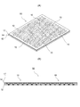
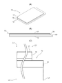
- FIG. 1A shows a schematic configuration of a liquid crystal panel 10 according to an embodiment of the present invention.
- the liquid crystal panel 10 is configured such that an array substrate 12 and a color filter substrate 14 are bonded together with an intermediate layer such as a liquid crystal layer interposed therebetween. Since the configurations of the array substrate 12 and the color filter substrate 14 can be the same as known configurations, the description thereof is omitted here.
- the array substrate 12 has an electrode terminal portion 122 provided so as to extend from a region bonded to the color filter substrate 14.
- a plurality of electric circuits are connected to the electrode terminal portion 122, and the liquid crystal panel 10 and these electric circuits are housed in a housing, so that, for example, a smartphone 100 as shown in FIG. Composed.
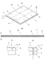
- the liquid crystal panel 10 is generally manufactured as a multi-chamfer glass base material 50 including a plurality of liquid crystal panels 10. And the single liquid crystal panel 10 is obtained by parting this glass substrate 50 for multi-cavity.
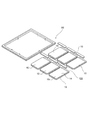
- liquid crystal panels 10 are arranged in a matrix of 3 rows and 2 columns, and a transparent thin film (a transparent conductive film such as an ITO film or an organic conductive film or a transparent protective film) is formed on the surface.
- a transparent thin film a transparent conductive film such as an ITO film or an organic conductive film or a transparent protective film
- a process for the multi-chamfered glass preform 50 on which 17 is formed will be described.
- the number of the liquid crystal panels 10 included in the multi-chamfer glass base material 50 is not limited to this, and can be appropriately increased or decreased.
- the glass substrate for multi-face 50 has the reforming line 20 along the shape cutting planned line corresponding to the shape (contour) of the liquid crystal panel 10. It is formed.
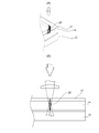
- the modification line 20 is a filament array in which a plurality of filament layers formed by a light beam pulse (a beam diameter of about 1 to 5 ⁇ m) irradiated from a pulse laser such as a picosecond laser or a femtosecond laser is arranged. (See FIGS. 4A and 4B.)
- the reforming line 20 has a perforated shape having a plurality of through holes or modified layers.
- the reforming line 20 has a property that it is more easily etched than other portions of the multi-chamfer glass base material 50.
- the shape of the reforming line 20 is not limited to this shape, and may have a shape other than this.
- the array substrate 12, the color filter substrate 14, and the transparent thin film 17 are simultaneously processed by one laser beam, a defect may occur in the liquid crystal layer. For this reason, in this embodiment, it becomes possible to suppress generation
- the color filter substrate 14 is changed from the opposite side to the color filter substrate 14 side.
- Laser irradiation may be performed after adjusting the focus and intensity so as to form the reforming line 20.
- the number of laser processing steps is increased by performing the process shown in FIG. 3D, it is possible to easily divide the glass substrate 50 for multi-faces while suppressing the occurrence of defects in the liquid crystal layer. become.
- the light beam from the pico laser is controlled so that the condensing region varies depending on the operation mode.
- the normal operation mode is employed when irradiating a laser beam to a position not adjacent to the electrode terminal portion 122, while condensing when irradiating the laser beam to a position adjacent to the electrode terminal portion 122.
- a region adjustment mode is employed.
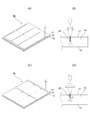
- FIGS. 5A and 5B show the laser light irradiation state in the normal operation mode
- FIGS. 5C and 5D show the laser light irradiation state in the condensing region adjustment mode.
- the normal operation mode is an operation mode that is employed when the laser beam is irradiated to a position that is not adjacent to the electrode terminal portion 122.
- the condensing region adjustment mode is an operation mode that is employed when laser light is irradiated to a position adjacent to the electrode terminal portion 122.
- the focal point of the laser light is located at the center of the array substrate 12 or the color filter substrate 14 in the thickness direction of the substrate being processed. Is controlled to fall within the range of the thickness of the substrate being processed. However, even when the focal point of the laser light is located at the center of the array substrate 12 or the color filter substrate 14 in the thickness direction of the substrate being processed, the condensing region of the laser light is the substrate being processed. In some cases, the thickness of the intermediate layer and the other substrate may be exceeded.
- the light collection region is specially adjusted so that the light collection region does not reach the intermediate layer.
- an optical system such as a laser head or an objective lens is moved in a direction in which the multi-surface glass base material 50 is separated, or an optical system for narrowing the condensing region. May be selectively placed on the optical path of the laser beam.
- the light collection region is specially adjusted so that the light collection region does not reach the intermediate layer. Is prevented from melting and scattering. Further, it is possible to prevent the terminal wiring from being corroded due to excessive permeation of the etching solution when etching is performed.
- the multi-chamfering glass base material 50 is formed as shown in FIGS. 6 (A) and 6 (B).
- the etching resistant film 16 having etching resistance is attached to both main surfaces.
- polyethylene having a thickness of 50 to 75 ⁇ m is employed as the etching resistant film 16.
- the configuration of the etching resistant film 16 is not limited to this.
- any material having resistance to an etching solution for etching glass such as polypropylene, polyvinyl chloride, and olefin resin, can be appropriately selected and employed.
- the etching resistant film 16 is irradiated with a laser beam along the shape cutting planned line corresponding to the shape of the liquid crystal panel 10 to be taken out. Done.
- the etching resistant film 16 is removed along the planned cutting line.
- the opening part of the etching-resistant film 16 will be formed along a shape cutting plan line, As a result, modification
- the formation position of the line 20 is exposed to the outside.
- the multi-chamfered glass base material 50 is introduced into the etching apparatus 300, and is subjected to an etching process with an etching solution containing hydrofluoric acid, hydrochloric acid, and the like.
- the multi-chamfering glass base material 50 is transported by the transport roller, and an etching solution is brought into contact with one or both surfaces of the multi-chamfering glass base material 50 in the etching chamber, whereby the multi-chamfering glass base material 50 is contacted.
- An etching process for 50 is performed.
- the multi-surface glass base material 50 is removed from the etchant. In this state, it is discharged from the etching apparatus 300.
- the etching solution is applied to the multi-chamfering glass base material 50 in each etching chamber 302 of the etching apparatus 300.
- Spray etching for spraying.
- FIG. 8 (B) instead of spray etching, as shown in FIG. 8 (B), in the overflow type etching chamber 304, a configuration is adopted in which the glass substrate 50 for multi-cavity is conveyed while being in contact with the overflowed etching solution. Is also possible.
- dip type etching is employed in which one or a plurality of multi-surface glass base materials 50 stored in a carrier are immersed in an etching tank 306 in which an etching solution is stored. It is also possible to do.
- the etching process proceeds at a slow rate of 3 ⁇ m / min or less with a thin hydrofluoric acid of 2% by weight or less, but is not limited to this method.
- the etching rate is not slowed down in the whole etching process but is gradually increased while initially adopting a faster etching rate, it is possible to shorten the etching process time.
- a configuration in which the hydrofluoric acid concentration in the etching solution is lowered as the process proceeds to the subsequent stage of the etching apparatus 300 may be employed.
- the modified line 20 is etched.
- the etching solution penetrates faster than other portions, and the glass is melted along this line, so that the color filter substrate can be easily cut by the reforming line 20. Further, even if a scratch or the like is generated at the time of laser irradiation, the scratch is easily lost.
- the affixed etching resistant film 16 is peeled off. Subsequently, as shown in FIGS. 9 (A) to 9 (C), a region facing the electrode terminal portion 122 of the array substrate 12 in the color filter substrate 14 is removed from the multi-chamfer glass base material 50.
- the process of forming the terminal part cutting groove 30 is performed.
- the scribe wheel (wheel cutter) 250 forms the terminal portion cutting groove 30 inside the region of the color filter substrate 14 facing the electrode terminal portion 122 of the array substrate 12.
- the terminal portion cutting groove 30 is formed along a terminal portion cutting planned line in order to remove a region of the color filter substrate 14 facing the electrode terminal portion 122 of the array substrate 12.
- the process proceeds to the division of the multi-chamfer glass base material 50 and the removal of the region facing the electrode terminal part 122.
- the modified line 20 is formed by laser filament processing, and the modified line is further etched to modify the multi-chamfer glass base material 50 with a slight mechanical pressure.
- the quality line 20 can be divided.
- the multi-chamfering glass base material 50 is soiled by applying a minute pressing force or pulling force to the multi-chamfering glass base material 50 or applying microscopic ultrasonic vibration. It is possible to divide without.
- the etching process does not completely cut it, it is possible to prevent the occurrence of a problem such that the end faces of the liquid crystal panel 10 separated during the etching collide with each other and are damaged. Further, the multi-chamfered glass base material 50 in an incompletely cut state after the etching process can be transported as it is (in a large format). Furthermore, since the etching solution does not reach the electrode terminal portion, it is not necessary to protect the electrode terminal portion with a masking agent having etching resistance. In addition, since at least the central portion of the end face of the liquid crystal panel 10 is etched, the strength (for example, bending strength) of the liquid crystal panel is higher than when cutting is performed only by laser processing.
- FIG. 11A to FIG. 11C show a schematic configuration of the liquid crystal panel 10 after the division.
- the end surface of the liquid crystal panel 10 is substantially perpendicular to the main surface.
- the taper width (L1 to L4 in FIG. 11C) generated on each end face of the array substrate 12 and the color filter substrate 14 each having a thickness of about 0.15 mm to 0.25 mm is 50 ⁇ m or less (mostly 20 to 35 ⁇ m).
- the glass substrate 50 for multi-sided drawing in which the liquid crystal panels 10 are arranged close to each other. For example, if there are gaps of about 10 ⁇ m in total with a laser width of 2 ⁇ m + ⁇ , it is possible to properly separate the glass substrate for multi-face 50 into a single liquid crystal panel 10.
Landscapes
- Physics & Mathematics (AREA)
- Chemical & Material Sciences (AREA)
- Nonlinear Science (AREA)
- Engineering & Computer Science (AREA)
- General Physics & Mathematics (AREA)
- Optics & Photonics (AREA)
- Crystallography & Structural Chemistry (AREA)
- Materials Engineering (AREA)
- Mathematical Physics (AREA)
- Organic Chemistry (AREA)
- Liquid Crystal (AREA)
- Life Sciences & Earth Sciences (AREA)
- Geochemistry & Mineralogy (AREA)
- General Chemical & Material Sciences (AREA)
- Chemical Kinetics & Catalysis (AREA)
- Microelectronics & Electronic Packaging (AREA)
- Re-Forming, After-Treatment, Cutting And Transporting Of Glass Products (AREA)
- Laser Beam Processing (AREA)
- Surface Treatment Of Glass (AREA)
Abstract
本発明に係る液晶パネル製造方法は、多面取り用ガラス母材(50)にお ける液晶パネルの形状に対応する形状切断予定線に沿ってレーザ光を照射す ることによって、エッチングされ易い性質の改質ライン(20)を形成する レーザ照射ステップ、およびカラーフィルタ基板(14)に対して、端子部 領域切断予定線に沿ってスクライブ溝を形成するスクライブ溝形成ステップ を少なくとも含む。レーザ照射ステップは、電極端子部に隣接しない位置に レーザ光を照射するときの通常動作モードと、電極端子部に隣接する位置に レーザ光を照射するときの集光領域調整モードとを含む。集光領域調整モー ドにおいては、集光領域が中間層に到達しないように集光領域が調整される。
Description
本発明は、多面取り用ガラス母材から所望形状の液晶パネルを複数得るための液晶パネル製造方法に関する。
一般的に、液晶パネルやカバーガラス等のガラスパネルの製造時には、多面取り用ガラス母材から所望形状の複数のガラスパネルを得るような処理が行われる。例えば、液晶パネルの製造においては、1組のガラス母材で同時に複数の液晶パネルを製造し、その後にガラス母材を単個の液晶パネルに分断するという手法(いわゆる多面取り)が広く採用されてきた。そして、ガラス母材を分断する際には、スクライブブレーク、レーザアブレーション加工、エッチング処理といった手法が用いられることが多かった。
ところが、スクライブブレークを採用した場合には、丸みを持った輪郭を有するガラスパネルを形成することが困難であった。また、レーザアブレーション加工では、加工速度が遅かったり、アブレーションデブリによる汚損が生じたりするといった不具合が発生し易かった。
そこで、従来、多面取り用ガラス母材をエッチング処理によって分断することによって複数のガラスパネルを得る技術が注目されるようになってきた。エッチング処理は、所望形状のカバーガラスを得るために利用されるようになり、最近では、アレイ基板およびカラーフィルタ基板を貼り合せてなる液晶パネルを多面取りするための多面取り用ガラス母材から所定形状の液晶パネルを複数得る際にもエッチング処理が用いられるようになってきている(例えば、特許文献1参照。)。
しかしながら、エッチング処理においては、ガラスパネルの厚み方向にエッチングが進行することに加えて、これに直交する方向にもエッチングが進行するサイドエッチングが発生する。このため、エッチング処理においては、ガラスパネルの切断面を主面とほぼ直角になるように形成することが困難になる。例えば、液晶パネルをエッチング処理によって多面取りする場合には、ガラス母材の厚み方向に直交する方向に進行するサイドエッチングの影響を考慮して、ガラス母材において各液晶パネル間にスペースを設ける必要があるため、多面取り効率が悪くなることがあった。
本発明の目的は、エッチング処理に伴うサイドエッチングの影響を最小限に抑制することが可能な液晶パネル製造方法を提供することである。
本発明は、中間層を挟んでアレイ基板およびカラーフィルタ基板を対向配置してなる液晶パネルを多面取りするための多面取り用ガラス母材から所定形状の液晶パネルを複数得るための液晶パネル製造方法である。中間層の代表例としては液晶層が挙げられるが、液晶が充填されていない空隙領域も中間層に含まれる。
この液晶パネル製造方法は、レーザ照射ステップ、およびスクライブ溝形成ステップを少なくとも含む。レーザ照射ステップでは、多面取り用ガラス母材における液晶パネルの形状に対応する形状切断予定線に沿ってレーザ光を照射することによって、形状切断予定線に沿って多面取り用ガラス母材にエッチングされ易い性質の改質ラインが形成される。
スクライブ溝形成ステップでは、カラーフィルタ基板に対して、このカラーフィルタ基板におけるアレイ基板の電極端子部に対向する領域を取り除くための端子部領域切断予定線に沿ってスクライブ溝が形成される。
レーザ照射ステップは、電極端子部に隣接しない位置にレーザ光を照射するときの通常動作モードと、電極端子部に隣接する位置にレーザ光を照射するときの集光領域調整モードとを含む。集光領域調整モードにおいては、集光領域が中間層に到達しないように集光領域が調整される。集光領域調整モードにおいては、例えば、集光領域が短くなるようにレンズ等の光学系を調整したり、集光領域が中間層から遠ざかるように変位させたりすると良い。
上述のような方法を採用することによって、例えば、改質ラインに沿ってエッチング液が浸透し易くなっており、エッチング処理の進行が容易で短時間化されるため、サイドエッチングの影響を最小化することが可能になる。
さらに、電極端子部に隣接する位置にレーザ光を照射するときにはレーザ光の集光領域が中間層まで到達しなくなるため、中間層にレーザ光のエネルギが伝達しなくなる。その結果、電極端子部に配置される端子配線パターンがレーザのエネルギによって溶けて飛散したり、電極端子部のその他の箇所に熱による不具合が発生したりすることが防止される。
上述の液晶パネル製造方法において、多面取り用ガラス母材をエッチング液に接触させることによって改質ラインをエッチングするエッチングステップをさらに含むことが好ましい。改質ラインをエッチングすることによって、形状切断予定線に沿って切断溝を形成することが可能になる。この切断溝に対して、例えば、物理的応力や熱的応力を加えることにより形状切断予定線に沿って液晶パネルを分断し、液晶パネルの多面取りが可能になる。
特に、電極端子部に隣接する位置においてはレーザ光の集光領域が中間層まで到達していないため、電極端子部の近傍においてエッチング液の過浸透によって電極端子部の端子配線等が腐食するといった不具合の発生が抑制される。
なお、アレイ基板またはカラーフィルタ基板にエッチングによって腐食され得る機能膜が形成されている場合には、この機能膜を耐エッチング性のある保護フィルムや耐エッチング層で覆った上で、この保護フィルムをパターニングすることによって形状切断予定線等のエッチングが必要な箇所が露出するような開口を設けるステップを加えると良い。
耐エッチングフィルムまたは耐エッチング層における形状切断予定線に対応する箇所に開口部を形成することによって、機能膜(例えば、オーバーコート等の保護膜やITOや有機導電膜等の透明性導電膜)を保護しつつ多面取り用ガラス母材における改質ラインをエッチングすることが可能になる。
この発明によれば、液晶パネル製造方法においてエッチング処理に伴うサイドエッチングの影響を最小限に抑制することが可能になる。さらに、電極端子部近傍において端子配線パターンが飛び散ったり、エッチング液の過浸透によって端子配線が腐食するといった不具合の発生を抑制することが可能になる。
以下、図を用いて、本発明に係る液晶パネルの製造方法の一実施形態を説明する。図1(A)は、本発明の一実施形態に係る液晶パネル10の概略構成を示している。同図に示すように、液晶パネル10は、アレイ基板12およびカラーフィルタ基板14が液晶層等の中間層を挟んで貼り合わされるように構成されている。アレイ基板12およびカラーフィルタ基板14の構成は、公知の構成と同様の構成が採用可能であるため、ここでは説明を省略する。
アレイ基板12は、カラーフィルタ基板14と貼り合わされる領域から延び出すように設けられた電極端子部122を有している。この電極端子部122には、複数の電気回路が接続され、液晶パネル10と、それらの電気回路とが筐体に収納されることによって、例えば、図1(B)に示すようなスマートフォン100が構成される。
続いて、液晶パネル10を製造する方法の一例について説明する。図2(A)および図2(B)に示すように、一般的に、液晶パネル10は、これを複数含んだ多面取り用ガラス母材50として製造される。そして、この多面取り用ガラス母材50を分断することによって、単個の液晶パネル10が得られる。
この実施形態では、便宜上、6つの液晶パネル10が3行2列のマトリクス状に配置され、かつ、表面に透明性薄膜(ITO膜や有機導電膜等の透明性導電膜、または透明保護膜等)17が形成された多面取り用ガラス母材50に対する処理について説明する。ただし、多面取り用ガラス母材50に含まれる液晶パネル10の数はこれに限定されるものではなく、適宜増減することが可能である。
多面取り用ガラス母材50は、まず、図3(A)および図3(B)に示すように、液晶パネル10の形状(輪郭)に対応する形状切断予定線に沿って改質ライン20が形成される。この改質ライン20は、例えば、ピコ秒レーザまたはフェムト秒レーザ等のパルスレーザから照射される光ビームパルス(ビーム径は1~5μm程度)によって形成される複数のフィラメント層を配列したフィラメントアレイである(図4(A)および図4(B)参照。)。改質ライン20は、例えば、図4(A)および図4(B)に示すように、複数の貫通孔または改質層を有するミシン目状を呈している。改質ライン20は、多面取り用ガラス母材50における他の箇所よりもエッチングされ易い性質を有している。もちろん、改質ライン20の形状は、この形状には限定されるものではなく、これ以外の形状を呈するものであっても良い。
アレイ基板12、カラーフィルタ基板14、および透明性薄膜17を同時に1つのレーザビームによって処理すると液晶層に不具合が生じる可能性がある。このため、本実施形態においては、図3(C)および図3(D)に示すようなレーザ加工を採用することにより、このような不具合の発生を抑制することが可能となる。すなわち、図3(C)に示すように、アレイ基板12側からアレイ基板12のみに改質ライン20が形成されるように焦点調整および強度調整をした上でレーザを照射し、液晶層近傍にエネルギが伝達しにくくすると良い。この状態で、物理的作用または熱的作用を加えることによって多面取り用ガラス母材50の分断が可能であれば、レーザ加工はここで終了する。
一方で、この状態では多面取り用ガラス母材50の分断が困難な場合には、図3(D)に示すように、今度は反対側となるカラーフィルタ基板14側からカラーフィルタ基板14のみに改質ライン20を形成するように焦点調整および強度調整をした上でレーザを照射すると良い。図3(D)に示す処理を行うことにより、レーザ加工の工程数が増加するものの、液晶層における不具合の発生を抑制しつつ、多面取り用ガラス母材50の分断を容易に行うことが可能になる。
ピコレーザからの光ビームは、その動作モードによって集光領域が異なるように制御される。例えば、この実施形態においては、電極端子部122に隣接しない位置にレーザ光を照射するときには通常動作モードが採用される一方で、電極端子部122に隣接する位置にレーザ光を照射するときには集光領域調整モードが採用される。
図5(A)および図5(B)は、通常動作モードにおけるレーザ光照射状態を示しており、図5(C)および図5(D)は、集光領域調整モードにおけるレーザ光照射状態を示している。通常動作モードは、電極端子部122に隣接しない位置にレーザ光を照射するときに採用される動作モードである。一方で、集光領域調整モードは、電極端子部122に隣接する位置にレーザ光を照射するときに採用される動作モードである。
通常動作モードおよび集光領域調整モードのいずれにおいても、レーザ光の焦点がアレイ基板12またはカラーフィルタ基板14のうちの処理中の基板の厚み方向の中央部に位置しており、その集光領域が処理中の基板の厚みの範囲内に収まるように制御されている。ただし、レーザ光の焦点がアレイ基板12またはカラーフィルタ基板14のうちの処理中の基板の厚み方向の中央部に位置している場合であっても、レーザ光の集光領域が処理中の基板の厚みの範囲を超えて中間層や他方の基板まで及ぶことがある。
このため、図5(C)および図5(D)に示すように、集光領域調整モードにおいては、集光領域が中間層に到達しないように、集光領域が特別に調整される。集光領域を調整する手法としては、レーザヘッドまたは対物レンズ等の光学系の少なくともいずれか一方を多面取り用ガラス母材50が離れる方向に移動させたり、集光領域を狭くするための光学系を選択的にレーザ光の光路上に配置させたりすることが挙げられる。
電極端子部122に隣接する位置にレーザ光を照射するときに、集光領域が中間層に到達しないように集光領域が特別に調整されることによって、電極端子部122の周囲において端子配線パターンが溶けて飛び散るようなことが防止される。また、エッチングを行ったときにおけるエッチング液の過浸透によって端子配線が腐食するようなことも防止される。
多面取り用ガラス母材50において形状切断予定線に沿って改質ライン20が形成された後には、多面取り用ガラス母材50は、図6(A)および図6(B)に示すように、両方の主面に耐エッチング性を備えた耐エッチングフィルム16が貼付される。ここでは、耐エッチングフィルム16として、厚みが50~75μmのポリエチレンを採用している。ただし、耐エッチングフィルム16の構成はこれには限定されない。例えば、ポリプロピレンやポリ塩化ビニルやオレフィン系樹脂等のように、ガラスをエッチングするエッチング液に対する耐性を備えたものであれば適宜選択して採用することも可能である。
耐エッチングフィルム16の貼付が完了すると、続いて、図6(C)に示すように、取り出すべき液晶パネル10の形状に対応する形状切断予定線に沿って耐エッチングフィルム16に対するレーザビームの照射が行われる。このレーザビームの照射によって、耐エッチングフィルム16が形状切断予定線に沿って除去される。そして、形状切断予定線に沿って耐エッチングフィルム16の開口部が形成されることになり、その結果、図3(C)に示した構成と同様に、多面取り用ガラス母材50の改質ライン20の形成位置が外部に露出することになる。
上述のレーザ加工が終わると、図7に示すように、多面取り用ガラス母材50は、エッチング装置300に導入され、フッ酸および塩酸等を含むエッチング液によってエッチング処理が施される。エッチング装置300では、搬送ローラによって多面取り用ガラス母材50を搬送しつつ、エッチングチャンバ内で多面取り用ガラス母材50の片面または両面にエッチング液を接触させることによって、多面取り用ガラス母材50に対するエッチング処理が行われる。なお、エッチング装置300におけるエッチングチャンバの後段には、多面取り用ガラス母材50に付着したエッチング液を洗い流すための洗浄チャンバが設けられているため、多面取り用ガラス母材50はエッチング液が取り除かれた状態でエッチング装置300から排出される。
多面取り用ガラス母材50にエッチング液を接触させる手法の一例として、図8(A)に示すように、エッチング装置300の各エッチングチャンバ302において、多面取り用ガラス母材50に対してエッチング液をスプレイするスプレイエッチングが挙げられる。また、スプレイエッチングに代えて、図8(B)に示すように、オーバーフロー型のエッチングチャンバ304において、オーバーフローしたエッチング液に接触しながら多面取り用ガラス母材50が搬送される構成を採用することも可能である。
さらには、図8(C)に示すように、エッチング液が収納されたエッチング槽306に、キャリアに収納された単数または複数の多面取り用ガラス母材50を浸漬されるディップ式のエッチングを採用することも可能である。
いずれの場合であっても、エッチング処理中に、形状切断予定線が厚み方向に貫通して、多面取り用ガラス母材50が分断してしまわないようにすることが重要である。このため、エッチング処理中(特にエッチング処理の後半部分)においては、エッチングレートを遅くして、エッチング量を正確に制御する必要がある。この実施形態では、2重量%以下の薄いフッ酸によって、3μm/分以下の遅い速度にてエッチング処理が進行するようにしているが、この手法に限定されるものではない。
エッチング処理の全体においてエッチングレートを遅くするのではなく、当初は速めのエッチングレートを採用しつつ段階的に遅くしていくようにすれば、エッチング処理の時間を短縮することが可能である。例えば、エッチング装置300の後段に進むにつれてエッチング液におけるフッ酸濃度を低下させるような構成を採用すると良い。
多面取り用ガラス母材50がエッチング装置300を通過すると、改質ライン20がエッチングされる。改質ライン20では、他の箇所よりも速くエッチング液が浸透し、このラインに沿ってガラスが溶解されることによって、改質ライン20によってカラーフィルタ基板を切断し易くなる。また、レーザ照射時においてキズ等が発生していた場合であっても、このキズが消失し易くなる。
エッチング処理が終了すると、貼付されていた耐エッチングフィルム16が剥離される。続いて、多面取り用ガラス母材50に対して、図9(A)~図9(C)に示すように、カラーフィルタ基板14におけるアレイ基板12の電極端子部122に対向する領域を取り除くための端子部切断溝30を形成する処理が行われる。この実施形態では、スクライブホイール(ホイールカッタ)250によって、カラーフィルタ基板14におけるアレイ基板12の電極端子部122に対向する領域の内側に端子部切断溝30が形成される。端子部切断溝30は、カラーフィルタ基板14におけるアレイ基板12の電極端子部122に対向する領域を取り除くため端子部切断予定線に沿って形成される。
スクライブホイール250による端子部切断溝30の形成が終わると、多面取り用ガラス母材50の分断および電極端子部122に対向する領域の除去に移行する。多面取り用ガラス母材50において、レーザのフィラメント加工によって改質ライン20が形成され、この改質ラインをさらにエッチングすることにより、わずかな機械的圧力のみで、多面取り用ガラス母材50を改質ライン20において分割することができる。例えば、多面取り用ガラス母材50に微小な押圧力や引っ張り力を加えたり、微小な超音波振動を与えたりすることによって、図10に示すように、多面取り用ガラス母材50を汚損することなく、分断することが可能である。
あえて、エッチング処理によって完全には切断してしまわないため、エッチング中に分離された液晶パネル10端面どうしが衝突して破損するといった不具合の発生が防止される。また、エッチング処理後の不完全に切断された状態の多面取り用ガラス母材50のまま(大判の状態のまま)、運搬することも可能になる。さらに、エッチング液が電極端子部に到達することがないため、耐エッチング性を備えたマスキング剤によって電極端子部を保護することが不要になる。また、液晶パネル10の端面における少なくとも中央部以外はエッチング処理が施されているため、レーザ加工のみで切断を行った場合に比較して液晶パネルの強度(例えば、曲げ強度)が高くなる。
図11(A)~図11(C)は、分断後の液晶パネル10の概略構成を示している。同図に示すように、液晶パネル10の端面は主面に対してほぼ直角になっている。例えば、それぞれが0.15mm~0.25mm程度の板厚のアレイ基板12およびカラーフィルタ基板14の各端面に発生するテーパ幅(図11(C)におけるL1~L4)を、50μm以下(多くは20~35μm)に抑えることが可能である。
このように、液晶パネル10を製造するにあたって、サイドエッチングの影響がほとんど発生しないため、液晶パネル10どうしを近接配置した多面取り用ガラス母材50の設計することができる。例えば、レーザ幅2μm+αで合計10μm程度の隙間があれば、多面取り用ガラス母材50を適正に単個の液晶パネル10に分離することが可能である。
上述の実施形態の説明は、すべての点で例示であって、制限的なものではないと考えられるべきである。本発明の範囲は、上述の実施形態ではなく、特許請求の範囲によって示される。さらに、本発明の範囲には、特許請求の範囲と均等の意味および範囲内でのすべての変更が含まれることが意図される。
10-液晶パネル
12-アレイ基板
14-カラーフィルタ基板
16-耐エッチングフィルム
17-透明性薄膜
20-改質ライン
30-端子部切断溝
50-多面取り用ガラス母材
100-スマートフォン
122-電極端子部
250-スクライブホイール
300-エッチング装置
302,304-エッチングチャンバ
306-エッチング槽
12-アレイ基板
14-カラーフィルタ基板
16-耐エッチングフィルム
17-透明性薄膜
20-改質ライン
30-端子部切断溝
50-多面取り用ガラス母材
100-スマートフォン
122-電極端子部
250-スクライブホイール
300-エッチング装置
302,304-エッチングチャンバ
306-エッチング槽
Claims (2)
- 中間層を挟んでアレイ基板およびカラーフィルタ基板を対向配置してなる液晶パネルを多面取りするための多面取り用ガラス母材から所定形状の液晶パネルを複数得るための液晶パネル製造方法であって、
前記多面取り用ガラス母材における液晶パネルの形状に対応する形状切断予定線に沿ってレーザ光を照射することによって、前記形状切断予定線に沿って前記多面取り用ガラス母材にエッチングされ易い性質の改質ラインを形成するレーザ照射ステップと、
前記カラーフィルタ基板に対して、このカラーフィルタ基板におけるアレイ基板の電極端子部に対向する領域を取り除くための端子部領域切断予定線に沿ってスクライブ溝を形成するスクライブ溝形成ステップと、
を少なくとも含み、
前記レーザ照射ステップは、前記電極端子部に隣接しない位置にレーザ光を照射するときの通常動作モードと、前記電極端子部に隣接する位置にレーザ光を照射するときの集光領域調整モードとを含み、
前記集光領域調整モードにおいては、集光領域が前記中間層に到達しないように集光領域が調整されることを特徴とする液晶パネル製造方法。 - 前記多面取り用ガラス母材をエッチング液に接触させることによって前記改質ラインをエッチングするエッチングステップをさらに含むことを特徴する請求項1に記載の液晶パネル製造方法。
Priority Applications (1)
| Application Number | Priority Date | Filing Date | Title |
|---|---|---|---|
| CN201980031999.7A CN112105984B (zh) | 2018-06-13 | 2019-05-29 | 液晶面板制造方法 |
Applications Claiming Priority (2)
| Application Number | Priority Date | Filing Date | Title |
|---|---|---|---|
| JP2018-112396 | 2018-06-13 | ||
| JP2018112396A JP6578533B1 (ja) | 2018-06-13 | 2018-06-13 | 液晶パネル製造方法 |
Publications (1)
| Publication Number | Publication Date |
|---|---|
| WO2019239889A1 true WO2019239889A1 (ja) | 2019-12-19 |
Family
ID=68053478
Family Applications (1)
| Application Number | Title | Priority Date | Filing Date |
|---|---|---|---|
| PCT/JP2019/021217 Ceased WO2019239889A1 (ja) | 2018-06-13 | 2019-05-29 | 液晶パネル製造方法 |
Country Status (4)
| Country | Link |
|---|---|
| JP (1) | JP6578533B1 (ja) |
| CN (1) | CN112105984B (ja) |
| TW (1) | TWI804634B (ja) |
| WO (1) | WO2019239889A1 (ja) |
Families Citing this family (3)
| Publication number | Priority date | Publication date | Assignee | Title |
|---|---|---|---|---|
| CN110764299A (zh) * | 2019-10-29 | 2020-02-07 | 深圳市华星光电技术有限公司 | 液晶显示面板以及显示模组制备方法 |
| KR102857567B1 (ko) * | 2020-12-22 | 2025-09-09 | 삼성디스플레이 주식회사 | 표시 장치의 제조 방법 |
| CN116300171A (zh) * | 2022-12-19 | 2023-06-23 | 芜湖长信新型显示器件有限公司 | 一种改善端子线路划伤的分板方法 |
Citations (4)
| Publication number | Priority date | Publication date | Assignee | Title |
|---|---|---|---|---|
| JP2010126398A (ja) * | 2008-11-27 | 2010-06-10 | Seiko Epson Corp | 表示パネルの製造方法 |
| JP2011180405A (ja) * | 2010-03-02 | 2011-09-15 | Seiko Epson Corp | 電気光学装置の製造方法 |
| US20160152018A1 (en) * | 2014-11-27 | 2016-06-02 | Samsung Display Co., Lid. | Method for manufacturing display panel and display panel manufactured by the method |
| WO2018216712A1 (ja) * | 2017-05-24 | 2018-11-29 | 株式会社Nsc | 透明性薄膜付ガラスパネル製造方法、透明性薄膜付液晶パネル製造方法、ガラスパネル製造方法、および液晶パネル製造方法 |
Family Cites Families (36)
| Publication number | Priority date | Publication date | Assignee | Title |
|---|---|---|---|---|
| JP2002172479A (ja) * | 2000-09-20 | 2002-06-18 | Seiko Epson Corp | レーザ割断方法、レーザ割断装置、液晶装置の製造方法並びに液晶装置の製造装置 |
| JP2003002676A (ja) * | 2001-06-19 | 2003-01-08 | Seiko Epson Corp | 基板の分割方法及び液晶装置の製造方法 |
| JP3871994B2 (ja) * | 2001-10-25 | 2007-01-24 | 株式会社半導体エネルギー研究所 | レーザ照射方法および半導体装置の作製方法 |
| JP2003303800A (ja) * | 2002-04-11 | 2003-10-24 | Sony Corp | 表面洗浄装置および表面洗浄方法 |
| JP4027252B2 (ja) * | 2003-03-26 | 2007-12-26 | 松下電器産業株式会社 | 放電ランプの製造方法 |
| JP4374881B2 (ja) * | 2003-03-28 | 2009-12-02 | ソニー株式会社 | 画素基板の製造方法およびその画素基板母材 |
| JP2005190857A (ja) * | 2003-12-26 | 2005-07-14 | Seiko Epson Corp | マスク、マスクの製造方法、有機エレクトロルミネッセンス装置の製造方法、有機エレクトロルミネッセンス装置の製造装置、有機エレクトロルミネッセンス装置、及び電子機器 |
| JP4884675B2 (ja) * | 2004-01-26 | 2012-02-29 | 株式会社半導体エネルギー研究所 | 半導体装置の作製方法 |
| US7247813B2 (en) * | 2004-10-13 | 2007-07-24 | Advanced Lcd Technologies Development Center Co., Ltd. | Crystallization apparatus using pulsed laser beam |
| TWI380868B (zh) * | 2005-02-02 | 2013-01-01 | Mitsuboshi Diamond Ind Co Ltdl | Fine processing method of sintered diamond using laser, cutter wheel for brittle material substrate, and method of manufacturing the same |
| KR200407370Y1 (ko) * | 2005-10-28 | 2006-01-31 | 케이 이엔지(주) | 평판디스플레이글라스판넬 레이저 커팅 장치 |
| JP2007157659A (ja) * | 2005-12-08 | 2007-06-21 | Tokki Corp | 有機el素子の配線パターンの形成方法及び有機el素子の形成装置 |
| JP2007283319A (ja) * | 2006-04-13 | 2007-11-01 | Seiko Epson Corp | レーザスクライブ方法、電気光学装置、電子機器 |
| JP2007326119A (ja) * | 2006-06-07 | 2007-12-20 | Seiko Epson Corp | レーザ照射装置、レーザスクライブ方法、電気光学装置の製造方法、加工生産物 |
| JP5784273B2 (ja) * | 2007-04-05 | 2015-09-24 | チャーム エンジニアリング株式会社 | レーザ加工方法及び切断方法並びに多層基板を有する構造体の分割方法 |
| JP2009064607A (ja) * | 2007-09-05 | 2009-03-26 | Sony Corp | 有機発光表示装置のリペア方法 |
| JP2009172626A (ja) * | 2008-01-23 | 2009-08-06 | Seiko Epson Corp | 電気光学装置の製造方法及び電気光学装置 |
| JP2009190943A (ja) * | 2008-02-15 | 2009-08-27 | Seiko Epson Corp | 基板の分断装置、基板の分断方法、及びその方法を用いて製造された基板 |
| JP2009244598A (ja) * | 2008-03-31 | 2009-10-22 | Sharp Corp | 母基板の分断方法および液晶表示装置の製造方法並びに液晶表示装置 |
| JP2010026041A (ja) * | 2008-07-16 | 2010-02-04 | Seiko Epson Corp | 表示パネルの製造方法 |
| JP2010023055A (ja) * | 2008-07-16 | 2010-02-04 | Seiko Epson Corp | 表示パネルの製造方法 |
| TW201024838A (en) * | 2008-12-22 | 2010-07-01 | Chi Mei Optoelectronics Corp | Color filter film substrate and application thereof |
| JP2010230782A (ja) * | 2009-03-26 | 2010-10-14 | Sony Corp | 液晶表示装置の製造方法 |
| JP2011107432A (ja) * | 2009-11-18 | 2011-06-02 | Seiko Epson Corp | 電気光学装置の製造方法 |
| JP5671873B2 (ja) * | 2010-08-09 | 2015-02-18 | 日産自動車株式会社 | レーザ溶接モニタリング装置 |
| KR20120037173A (ko) * | 2010-10-11 | 2012-04-19 | 삼성전자주식회사 | 액정 표시 장치의 제조 방법 |
| TWI457191B (zh) * | 2011-02-04 | 2014-10-21 | Mitsuboshi Diamond Ind Co Ltd | 雷射切割方法及雷射加工裝置 |
| JP5494592B2 (ja) * | 2011-08-30 | 2014-05-14 | 三星ダイヤモンド工業株式会社 | Ledパターン付き基板の加工方法 |
| JP2013127540A (ja) * | 2011-12-19 | 2013-06-27 | Canon Inc | 表示装置の製造方法 |
| JP2014120643A (ja) * | 2012-12-18 | 2014-06-30 | Fuji Electric Co Ltd | 半導体デバイスの製造方法、及び半導体デバイスの製造装置 |
| WO2015178358A1 (ja) * | 2014-05-23 | 2015-11-26 | 日本電気硝子株式会社 | パネルの製造方法 |
| JP2016157056A (ja) * | 2015-02-26 | 2016-09-01 | 株式会社Nsc | 液晶パネルの製造方法 |
| JP2016224201A (ja) * | 2015-05-29 | 2016-12-28 | 株式会社Nsc | 液晶パネルの製造方法 |
| JP6283062B2 (ja) * | 2016-05-31 | 2018-02-21 | 株式会社Nsc | 表示装置製造方法 |
| JP2018026260A (ja) * | 2016-08-10 | 2018-02-15 | 株式会社Nsc | 表示装置製造方法 |
| JP2018081242A (ja) * | 2016-11-18 | 2018-05-24 | 株式会社Nsc | 液晶パネルの製造方法 |
-
2018
- 2018-06-13 JP JP2018112396A patent/JP6578533B1/ja active Active
-
2019
- 2019-05-29 CN CN201980031999.7A patent/CN112105984B/zh active Active
- 2019-05-29 WO PCT/JP2019/021217 patent/WO2019239889A1/ja not_active Ceased
- 2019-06-11 TW TW108120042A patent/TWI804634B/zh active
Patent Citations (4)
| Publication number | Priority date | Publication date | Assignee | Title |
|---|---|---|---|---|
| JP2010126398A (ja) * | 2008-11-27 | 2010-06-10 | Seiko Epson Corp | 表示パネルの製造方法 |
| JP2011180405A (ja) * | 2010-03-02 | 2011-09-15 | Seiko Epson Corp | 電気光学装置の製造方法 |
| US20160152018A1 (en) * | 2014-11-27 | 2016-06-02 | Samsung Display Co., Lid. | Method for manufacturing display panel and display panel manufactured by the method |
| WO2018216712A1 (ja) * | 2017-05-24 | 2018-11-29 | 株式会社Nsc | 透明性薄膜付ガラスパネル製造方法、透明性薄膜付液晶パネル製造方法、ガラスパネル製造方法、および液晶パネル製造方法 |
Also Published As
| Publication number | Publication date |
|---|---|
| JP6578533B1 (ja) | 2019-09-25 |
| CN112105984B (zh) | 2024-01-30 |
| JP2019215439A (ja) | 2019-12-19 |
| TW202006431A (zh) | 2020-02-01 |
| CN112105984A (zh) | 2020-12-18 |
| TWI804634B (zh) | 2023-06-11 |
Similar Documents
| Publication | Publication Date | Title |
|---|---|---|
| KR101802527B1 (ko) | 가공 대상물 절단 방법 | |
| KR101721709B1 (ko) | 가공 대상물 절단 방법 | |
| KR20210048000A (ko) | 크랙 프리 유리기판 절단 및 박형화 방법 | |
| JP6803018B2 (ja) | ガラス用エッチング液およびガラス基板製造方法 | |
| JP7176695B2 (ja) | ガラス基板製造方法 | |
| JP6578533B1 (ja) | 液晶パネル製造方法 | |
| CN104690429A (zh) | 光器件晶片的加工方法 | |
| WO2018216712A1 (ja) | 透明性薄膜付ガラスパネル製造方法、透明性薄膜付液晶パネル製造方法、ガラスパネル製造方法、および液晶パネル製造方法 | |
| JP2014069981A (ja) | 基板加工装置及び基板加工方法 | |
| US11532804B2 (en) | Method of manufacturing flexible OLED module | |
| JP2019109411A (ja) | 液晶パネル製造方法 | |
| JP6519045B2 (ja) | ガラスパネル製造方法および液晶パネル製造方法 | |
| JP6501093B1 (ja) | 透明性薄膜付ガラスパネル製造方法および透明性薄膜付液晶パネル製造方法 | |
| JP6519044B2 (ja) | 液晶パネル製造方法 | |
| WO2018135565A1 (ja) | 液晶パネル製造方法 | |
| JP2019028202A (ja) | 液晶パネル製造方法 | |
| JP7251704B2 (ja) | ガラス用エッチング液およびガラス基板製造方法 | |
| CN114524620A (zh) | 玻璃及制造玻璃的方法 | |
| JP2019120738A (ja) | 液晶パネル製造方法 | |
| JP6534105B2 (ja) | 液晶パネル製造方法 | |
| JP7287637B2 (ja) | 液晶パネル製造方法 | |
| JP2018136492A (ja) | 液晶パネル製造方法およびこれに用いられる保護ガラスプレート | |
| JP2019066783A (ja) | 基板製造方法 | |
| JP2016224201A (ja) | 液晶パネルの製造方法 | |
| JP2016157056A (ja) | 液晶パネルの製造方法 |
Legal Events
| Date | Code | Title | Description |
|---|---|---|---|
| 121 | Ep: the epo has been informed by wipo that ep was designated in this application |
Ref document number: 19819836 Country of ref document: EP Kind code of ref document: A1 |
|
| NENP | Non-entry into the national phase |
Ref country code: DE |
|
| 122 | Ep: pct application non-entry in european phase |
Ref document number: 19819836 Country of ref document: EP Kind code of ref document: A1 |