WO2019207673A1 - 保護リレー - Google Patents
保護リレー Download PDFInfo
- Publication number
- WO2019207673A1 WO2019207673A1 PCT/JP2018/016757 JP2018016757W WO2019207673A1 WO 2019207673 A1 WO2019207673 A1 WO 2019207673A1 JP 2018016757 W JP2018016757 W JP 2018016757W WO 2019207673 A1 WO2019207673 A1 WO 2019207673A1
- Authority
- WO
- WIPO (PCT)
- Prior art keywords
- coefficient
- filter
- power system
- failure
- output signal
- Prior art date
- Legal status (The legal status is an assumption and is not a legal conclusion. Google has not performed a legal analysis and makes no representation as to the accuracy of the status listed.)
- Ceased
Links
Images











Classifications
-
- H—ELECTRICITY
- H02—GENERATION; CONVERSION OR DISTRIBUTION OF ELECTRIC POWER
- H02H—EMERGENCY PROTECTIVE CIRCUIT ARRANGEMENTS
- H02H3/00—Emergency protective circuit arrangements for automatic disconnection directly responsive to an undesired change from normal electric working condition with or without subsequent reconnection ; integrated protection
- H02H3/08—Emergency protective circuit arrangements for automatic disconnection directly responsive to an undesired change from normal electric working condition with or without subsequent reconnection ; integrated protection responsive to excess current
-
- G—PHYSICS
- G01—MEASURING; TESTING
- G01R—MEASURING ELECTRIC VARIABLES; MEASURING MAGNETIC VARIABLES
- G01R31/00—Arrangements for testing electric properties; Arrangements for locating electric faults; Arrangements for electrical testing characterised by what is being tested not provided for elsewhere
- G01R31/08—Locating faults in cables, transmission lines, or networks
-
- H—ELECTRICITY
- H02—GENERATION; CONVERSION OR DISTRIBUTION OF ELECTRIC POWER
- H02H—EMERGENCY PROTECTIVE CIRCUIT ARRANGEMENTS
- H02H3/00—Emergency protective circuit arrangements for automatic disconnection directly responsive to an undesired change from normal electric working condition with or without subsequent reconnection ; integrated protection
- H02H3/02—Details
- H02H3/04—Details with warning or supervision in addition to disconnection, e.g. for indicating that protective apparatus has functioned
-
- H—ELECTRICITY
- H02—GENERATION; CONVERSION OR DISTRIBUTION OF ELECTRIC POWER
- H02H—EMERGENCY PROTECTIVE CIRCUIT ARRANGEMENTS
- H02H3/00—Emergency protective circuit arrangements for automatic disconnection directly responsive to an undesired change from normal electric working condition with or without subsequent reconnection ; integrated protection
- H02H3/40—Emergency protective circuit arrangements for automatic disconnection directly responsive to an undesired change from normal electric working condition with or without subsequent reconnection ; integrated protection responsive to ratio of voltage and current
-
- G—PHYSICS
- G01—MEASURING; TESTING
- G01R—MEASURING ELECTRIC VARIABLES; MEASURING MAGNETIC VARIABLES
- G01R19/00—Arrangements for measuring currents or voltages or for indicating presence or sign thereof
- G01R19/165—Indicating that current or voltage is either above or below a predetermined value or within or outside a predetermined range of values
Definitions
- This disclosure relates to protection relays, for example, digital protection relays used for power system protection.
- the digital protection relay is an A / D converter that performs A / D (Analog-to-Digital) conversion of the voltage or current sample value of the power system, and a DC component other than the fundamental wave component from the sample value after A / D conversion. And a digital filter for removing the above.
- a / D Analog-to-Digital
- the time width from the newest current data point to the oldest data point among a plurality of data points used for the digital filter processing is referred to as a window length.
- Patent Document 1 uses a first filter with a short window length from the detection of a system failure to the first time, and the window length from the first time to the second time. Uses a medium second filter, and uses a third filter with a long window length from the second time.
- the overcurrent relay disclosed in Japanese Patent Application Laid-Open No. 2011-250518 includes a first overcurrent determination unit and a second overcurrent determination unit.
- the first overcurrent determination unit performs the operation determination by comparing the effective value calculated using the current data of the first period and the first determination threshold.
- the second overcurrent determination unit compares the effective value calculated using the current data of the second period shorter than the first period with the second determination threshold higher than the first determination threshold to determine the operation. Do.
- the overcurrent relay generates an operation output based on the operation determination result output at an earlier timing among the operation determination results of the first overcurrent determination unit and the second overcurrent determination unit.
- JP-A-60-204219 JP 2011-250518 A Japanese Patent Laid-Open No. 01-227613
- the first and second time points for switching the filter are adjusted, and in the case of the protection relay of Patent Document 2, the first and second determination thresholds are set.
- This disclosure takes the above-mentioned problems into consideration, and an object thereof is to provide a protection relay capable of achieving both response speed and operation determination accuracy.
- a protection relay performs an analog input circuit that generates time-series data by detecting a signal representing a current or voltage of a power system and performing A / D conversion, and performs digital processing based on the time-series data. And an arithmetic circuit.
- the calculation circuit includes a first filter, a second filter, a coefficient calculation unit, an operation determination unit, and a coefficient setting unit.
- the first filter attenuates or removes a direct current component and harmonic components of at least a part of the power system from the time series data to pass at least a part of the fundamental wave component of the power system, and the first window length
- the second filter attenuates or removes the direct current component and the harmonic component of at least a part of the power system in the time series data to pass at least a part of the fundamental wave component of the power system, and the first window length It has a shorter second window length.
- the coefficient computing unit multiplies the value based on the output signal of the first filter by the first coefficient, multiplies the value based on the output signal of the second filter by the second coefficient, and synthesizes the multiplication results.
- the motion determination unit performs a motion determination based on the synthesis result by the coefficient calculation unit.
- the coefficient setting unit sets the first coefficient and the second coefficient.
- the coefficient setting unit decreases the first coefficient and increases the second coefficient when a failure of the power system is detected, and then changes the first coefficient and the second coefficient with time.
- FIG. 10 is a diagram illustrating an example of setting coefficient values k1 and k2 in Embodiment 2.
- FIG. It is a figure which shows the filter input waveform in simulation.
- FIG. 10 is a diagram illustrating a setting example of coefficient values k1 and k2 in the third embodiment.
- FIG. 16 is a diagram illustrating an amplitude value calculation result of the filter output signal waveform with respect to the input signal waveform of FIG. 9 in the setting of the coefficient values k1 and k2 illustrated in FIG.
- FIG. 10 is a diagram illustrating a setting example of coefficient values k1 and k2 in the fourth embodiment.
- FIG. 18 is a diagram illustrating an amplitude value calculation result of the filter output signal waveform with respect to the input signal waveform of FIG. 9 in the setting of the coefficient values k1 and k2 illustrated in FIG.
- FIG. 10 is a functional block diagram for explaining digital processing realized by the arithmetic circuit in FIG. 2 in the protection relay according to the fifth embodiment. It is a flowchart which shows the process sequence of the digital processing part of FIG.
- FIG. 10 is a diagram illustrating a filter output waveform with respect to the input signal waveform of FIG. 9 in the protection relay of the fifth embodiment. It is a figure which shows the calculation result of the amplitude value based on the filter output waveform of FIG.
- an overcurrent relay will be mainly described as an example, but this disclosure is not limited to an overcurrent relay.
- the same reference number is attached
- FIG. 1 is a diagram illustrating a configuration example of a power system including a protection relay.
- a power source 42 is provided at one end of the power transmission line 40.
- the power transmission line 40 is a three-phase power transmission line, but in FIG. 1, it is shown as a single line for ease of illustration.
- the transmission line 40 is provided with a current transformer (CT). Furthermore, a circuit breaker (CB: Circuit Breaker) 43 is provided on the power transmission line 40.
- CT current transformer
- CB Circuit Breaker
- the protection relay 50 acquires a signal representing a three-phase alternating current flowing through the transmission line 40 from the current transformer CT.
- the protection relay 50 generates current data by sampling the acquired current signal and performing A / D (Analog to Digital) conversion.
- the current data may be referred to as current time series data or simply time series data.
- the protection relay 50 performs an overcurrent relay calculation based on the generated current data. As a result, when an abnormality is detected, the protection relay 50 outputs a trip signal for opening the circuit breaker 43.
- the above is a case of an overcurrent relay, but the same applies to the case of other relay elements (for example, when voltage data based on a three-phase AC voltage is used).
- FIG. 2 is a block diagram illustrating an example of a hardware configuration of the protection relay of FIG.
- the protection relay 50 in FIG. 2 has the same configuration as a so-called digital relay device.
- the protection relay 50 includes an analog input circuit 51, an arithmetic circuit 60, and an I / O (Input and Output) circuit 70.
- the analog input circuit 51 includes an input transformer 52, analog filters (AF: Analog Filter) 54_1, 54_2,... 54_n, sample hold circuits (S / H: Sample Hold Circuits) 55_1, 55_2,. (MPX: Multiplexer) 56, A / D converter 57, and DMA (Direct Memory Access) controller 58 are included.
- analog filters AF: Analog Filter
- S / H Sample Hold Circuits
- MPX Multiplexer
- a / D converter 57 A / D converter 57
- DMA Direct Memory Access
- the input transformer 52 includes auxiliary transformers 53_1, 53_2, ..., 53_n for each input channel.
- the input transformer 52 receives a current signal from the current transformer CT of FIG.
- Each auxiliary transformer 53 converts the current signal from the current transformer CT into a signal having a voltage level suitable for signal processing in the analog input circuit 51 and the arithmetic circuit 60.
- the analog filter 54 and the sample hold circuit 55 are provided for each channel of the input signal.
- Each analog filter 54 is a low-pass filter provided to remove aliasing errors during A / D conversion.
- Each sample and hold circuit 55 samples and holds the signal that has passed through the corresponding analog filter 54 at a specified sampling frequency.
- the sampling frequency is, for example, 4800 Hz.
- the multiplexer 56 sequentially selects the voltage signals held in the sample hold circuits 55_1, 55_2,.
- the A / D converter 57 converts the signal selected by the multiplexer 56 into a digital value.
- the DMA controller 58 transfers the digital data output from the A / D converter 57 to the RAM 62.
- the arithmetic circuit 60 includes a CPU (Central Processing Unit) 61, a RAM (Random Access Memory) 62, a ROM (Read Only Memory) 63, a memory 64, and a bus 65 for connecting them.
- the CPU 61 controls the overall operation of the protection relay 50 by operating according to a program.
- the RAM 62 and the ROM 63 are used as the main memory of the CPU 61.
- the memory 64 can store programs, setting values for signal processing, and the like by using a nonvolatile memory such as a flash memory.
- the arithmetic circuit 60 is not limited to the example of FIG.
- the arithmetic circuit 60 may include a plurality of CPUs.
- the arithmetic circuit 60 may be configured by at least one ASIC (Application Specific Integrated Circuit) instead of a processor such as a CPU, or may be configured by at least one FPGA (Field Programmable Gate Array). Good.
- the arithmetic circuit 60 may be configured by any combination of a processor, an ASIC, and an FPGA.
- the I / O circuit 70 includes a digital input (D / I) circuit 71 and a digital output (D / O) circuit 72.
- the digital input circuit 71 and the digital output circuit 72 are interface circuits for performing communication between the CPU 61 and an external device.
- the digital output circuit 72 outputs a trip signal to the circuit breaker 43A or 43B on its own end side shown in FIG.
- the contents of the digital processing realized by the arithmetic circuit 60 will be described in detail.
- the following functions are described as being realized by the CPU 61 operating according to a program.
- the arithmetic circuit 60 may be realized by an ASIC, an FPGA, or the like.
- an overcurrent relay will be mainly described as an example, but the present disclosure is not limited to the overcurrent relay.
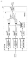
- FIG. 3 is a functional block diagram showing the configuration of the digital processing unit realized by the arithmetic circuit of FIG.
- the digital processing unit 80 includes a first filter 81, a second filter 82, a third filter 83, amplitude value calculation units 84 and 85, a failure determination unit 86, and a coefficient calculation unit 90. And an operation determination unit 95.
- the digital processing unit 80 receives time-series data 79 (that is, current data and / or voltage data of the power system) captured in the RAM 62.
- the time series data 79 is power system current data.
- Each of the first filter 81 and the second filter 82 is a digital filter that can be configured as a finite impulse response (FIR) filter.
- the first filter 81 and the second filter 82 are configured to remove from the time-series data 79 a direct current component and at least a part of higher order harmonic components that impede relay operation and relay characteristics.
- the first filter 81 and the second filter 82 pass at least a part of the fundamental component of the power system necessary for the relay calculation.
- the first filter 81 is configured to block or attenuate the DC component as much as possible, attenuate the harmonic component of the power system as much as possible, and pass the fundamental wave component of the power system as much as possible.
- the frequency characteristic of the second filter 82 may be different from the frequency characteristic of the first filter 81. Specifically, the second filter 81 blocks or attenuates the DC component as much as possible, but the attenuation factor of the harmonic component of the second filter 82 may be smaller than the attenuation factor of the harmonic component of the first filter 81.
- the window length of the first filter 81 is characterized by being longer than the window length of the second filter 82.
- the filter function is represented by the difference between the current value i (t) at the current time and the current value i (t ⁇ 2T) 60 ° before the current time.
- i (t-2T) may be simply referred to as i (t-2).
- the first filter 81 can attenuate the harmonic components more than the second filter 82.
- the fundamental wave component can be extracted with high accuracy.
- the output of the second filter 82 includes harmonic components without being attenuated as compared with the case of the first filter 81. Therefore, when performing amplitude value calculation using time-series data when the current suddenly increases due to the occurrence of a failure, since harmonic components are transiently included, it is better to use the data that has passed through the first filter 81. The calculation can be performed with higher accuracy than using the second filter 82.
- the response when the input time-series data (current data and / or voltage data) changes is slower in the first filter 81 than in the second filter 82.
- the first filter 81 performs a filter operation using both the data before the occurrence of the failure and the data after the occurrence of the failure immediately after the occurrence of the failure in the power system (specifically, during the time corresponding to the window length). It will be.
- the third filter 83 is a digital filter that can be configured as an FIR filter.
- the third filter 83 detects a sudden change when a failure occurs by removing the fundamental wave component from the output data of the second filter 82.
- the third filter 83 outputs at least a part of components other than the basic component. However, since the output of the third filter 83 is used for failure determination, the abnormality output is configured to continue for a certain time or more when a failure occurs.
- the first amplitude value calculation unit 84 performs the amplitude value calculation using the time series data output from the first filter 81.
- the second amplitude value calculation unit 85 performs amplitude value calculation using the time series data output from the second filter 82.
- the method of calculating the amplitude value is not particularly limited, but for example, the method described in Japanese Patent Laid-Open No. 01-227613 (Patent Document 3) can be used.
- the current value at the present time is i (t), and the current values at 30 °, 60 °, and 90 ° before the current angle are i (t-1) and i (t-2), respectively.
- Patent Document 3 A more general expression is disclosed in Patent Document 3 above.
- the failure determination unit 86 determines whether a failure has occurred in the power system based on the output of the third filter 83. For example, the failure determination unit 86 determines that a failure has occurred in the power system when the output level of the third filter 83 exceeds a threshold value. Since the third filter 83 removes the fundamental wave component, when the amplitude of the time series data does not change, the magnitude of the output is almost zero. When a failure occurs in the power system, the magnitude and phase of the current change greatly, so that a harmonic component is transiently generated, and the third filter 83 outputs a signal having a magnitude exceeding the threshold.
- the coefficient calculation unit 90 includes a multiplier 91, a multiplier 92, an adder 94, and a coefficient setting unit 93.
- the multiplier 91 multiplies the amplitude value (that is, DF (t) long ) of the first filter 81 output from the amplitude value calculation unit 84 by the coefficient k1.
- the multiplier 92 multiplies the amplitude value (that is, DF (t) short ) of the second filter 82 output from the amplitude value calculation unit 85 by the coefficient k2.
- the adder 94 adds k1 * DF (t) long , which is the output of the multiplier 91, and k2 * DF (t) short , which is the output of the multiplier 92, and outputs the addition result.
- the coefficient setting unit 93 sets the values of the coefficients k1 and k2 in accordance with a predetermined correspondence between the coefficients k1 and k2 and the elapsed time after the failure detection. This correspondence is stored in the memory in the form of a table or a mathematical expression.
- FIG. 4 is a functional block diagram showing a modification of FIG.
- time series data 79 that is, current data and / or voltage data of the power system taken in the RAM 62 is input to the third filter 83.
- time series data 79 that is, current data and / or voltage data of the power system
- FIG. 4 Since the other points of FIG. 4 are the same as those of FIG. 3, the same or corresponding parts are denoted by the same reference numerals and description thereof will not be repeated. Even with the configuration of FIG. 4, substantially the same function as in the case of FIG. 3 can be achieved.
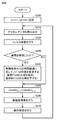
- FIG. 5 is a flowchart showing a processing procedure by the arithmetic circuit of FIG.
- the flowchart in FIG. 5 shows the operation of the digital processing unit in FIGS. 3 and 4 in time series. Each step in FIG. 5 is executed by the CPU 61 in FIG.
- the CPU 61 takes out data necessary for the filter operation from the RAM 62.
- time-series current data and / or voltage data detected from the power system and subjected to A / D conversion are stored in the RAM 62.
- the CPU 61 performs a filter operation using the read data as the first filter 81, the second filter 82, and the third filter 83 described above.
- the first filter 81 and the second filter 82 are FIR filters that remove DC components and specific harmonic components. When a failure occurs, the DC component and the harmonic component transiently increase greatly, so it is important to remove the DC component and the harmonic component in order to reduce the calculation error of the amplitude value calculation. Further, the first filter 81 and the second filter 82 have a feature that the window length of the first filter 81 is longer than the window length of the second filter 82 filter. Both the first filter 81 and the second filter 82 pass at least part of the fundamental wave component, but the magnitude of transmission differs for each filter.
- the second filter 82 When each filter is normalized with respect to the fundamental wave component, the second filter 82 has less attenuation of the harmonic component and the value of a certain harmonic component is larger than that of the fundamental wave as compared with the first filter 81. Sometimes. In addition, when the input changes suddenly, the second filter with a shorter window length follows the data after the failure more quickly, but overshoot (that is, the amplitude value calculation result becomes transiently larger than the actual input). It is easy to cause.
- the third filter 83 is an FIR filter that removes a fundamental wave component.
- the magnitude of the output of the third filter 83 is almost zero.
- the current changes greatly, so that components other than the fundamental wave increase.
- the magnitude of the output of the third filter 83 increases in accordance with the sudden change in current.
- the CPU 61 calculates the amplitude value of the output signal of the first filter 81 and calculates the amplitude value of the output signal of the second filter 82. Any known method may be used as an amplitude value calculation method, and is not particularly limited.
- the CPU 61 determines whether or not a failure has occurred in the power system based on the output of the third filter 83. For example, when the state where the output level of the third filter 83 exceeds a preset threshold value continues for a predetermined verification period (for example, 2T), the CPU 61 causes a failure in the power system. It is determined that
- step S70 the CPU 61 uses the values of the initially set coefficients k1 and k2, and the first filter 81.
- the output signal amplitude value DF (t) long is multiplied by a factor k1
- the output signal amplitude value DF (t) short of the second filter 82 is multiplied by a factor k2.
- the CPU 61 adds these multiplication results to each other.
- the CPU 61 performs an operation determination based on the addition result. In this case, since the addition result is almost determined by the output of the first filter 81, it is possible to prevent the overcurrent relay from making an erroneous determination due to a sudden surge current or the like. Thereafter, the procedure from step S20 is repeated.
- the CPU 61 sets the coefficients k1 and k2 based on a table or mathematical formula created in advance according to the passage of time from the failure detection time.
- the CPU 61 calculates k1 * DF (t) long + k2 * DF (t) short using the values of the coefficients k1 and k2 changed in step S60.
- the CPU 61 performs an operation determination based on the calculation result in step S70. For example, when the multiplication result exceeds the threshold value, the CPU 61 sets the operation flag to 1 to open the circuit breaker.
- the first filter 81 and the second filter 82 having different window lengths are used, and k1 times the output signal of the first filter 81 and the output of the second filter 82 are used.
- the operation is determined based on the sum of k2 times the signal.
- the first coefficient is decreased and the second coefficient is increased, and thereafter, the first coefficient and the second coefficient are changed over time. Accordingly, it is possible to provide a protection relay that can suppress the occurrence of overshoot and can achieve both response speed and operation determination accuracy.
- Embodiment 2 a specific example of the first filter 81, the second filter 82, and the third filter 83 described in the first embodiment and a specific method for setting the coefficients k1 and k2 will be described.
- first and second filters [Specific examples of first and second filters]
- the full cycle cosine filter is i (t) + i (t-1) ⁇ cos30 ° + i (t-2) ⁇ cos60 ° + i (t-3) ⁇ cos90 ° + i (t-4) ⁇ cos120 ° + I (t-5), cos 150 ° + i (t-6), cos 180 ° + i (t-7), cos 210 ° + i (t-8), cos 240 ° + I (t-9) ⁇ cos270 ° + i (t-10) ⁇ cos300 ° + i (t-11) ⁇ cos330 °... (2) It is expressed as Therefore, the window length of the full cycle cosine filter is 330 ° in electrical angle.
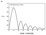
- FIG. 6 is a diagram showing the gain characteristics of the full cycle cosine filter.
- the horizontal axis is a frequency normalized with the rated frequency f of the power system, and the vertical axis is the gain.
- the direct current component and the harmonic component that is an integral multiple of the rated frequency f are completely removed.
- the fundamental wave component passes through without being attenuated.
- a signal having a rated frequency is output after being delayed by 360 °.
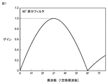
- a 60 ° difference filter is used as the second filter 82.
- FIG. 7 is a diagram showing the gain characteristics of the 60 ° difference filter. As shown in FIG. 7, the DC component is completely attenuated, but the signal of the fundamental component is attenuated though passing through the 60 ° difference filter. Regarding the phase characteristics, a signal having a rated frequency is output in a state where the phase is advanced by 60 °.
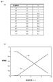
- FIG. 8 is a diagram illustrating a setting example of the coefficient values k1 and k2 in the second embodiment.
- coefficient values k1 and k2 are shown in a tabular form
- FIG. 8B numerical values k1 and k2 are shown in a graph.
- T corresponds to 30 ° in electrical angle
- the coefficient setting unit 93 when a fault in the power system is detected, the coefficient setting unit 93 rapidly decreases the first coefficient k1 and increases the second coefficient k2. Thereafter, the coefficient setting unit 93 increases the first coefficient k1 and decreases the second coefficient k2, and then decreases the first coefficient k1 and increases the second coefficient k2. Thereafter, the coefficient setting unit 93 increases the first coefficient and decreases the second coefficient.
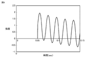
- FIG. 9 is a diagram showing a filter input waveform in the simulation.
- the current value when a failure occurs in the power system is represented by the superposition of an alternating current component and a direct current component.
- the resistance component of the transmission line 40 in FIG. 1 is R and the inductance component is L
- the time constant ⁇ at which the DC component changes is expressed by L / R.
- ⁇ tan ⁇ 1 ⁇ L / R (where ⁇ is the angular frequency of the fundamental wave of the power system) and the instantaneous voltage phase at the time of the failure is ⁇
- the current waveform when the magnitude of the DC component is maximum is used as a virtual filter input waveform.
- the coefficients k1 and k2 are determined so that good response and accuracy can be obtained even under the most severe conditions.
- FIG. 10 is a diagram showing a filter output waveform with respect to the input waveform of FIG.
- the input signal waveform is indicated by a broken line
- the output waveform of the full cycle cosine filter is indicated by a thick solid line
- the output waveform of the 60 ° difference filter is indicated by a thin solid line.
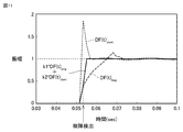
- FIG. 11 is a diagram showing the calculation result of the amplitude value based on the filter output waveform of FIG.
- the amplitude value DF (t) long of the output signal of the first filter 81 is indicated by a thick broken line
- the amplitude value DF (t) short of the output signal of the second filter 82 is indicated by a thin broken line
- the coefficient calculation unit 90 The output signal amplitude value (k1 * DF (t) long + k2 * DF (t) short ) is indicated by a solid line.
- the coefficients k1 and k2 are those shown in FIG. 8, but are determined as follows.
- the first coefficient k1 is set to 1 and the second coefficient k2 is set to 0 until failure detection.
- the amplitude value of the output signal of the coefficient calculation unit 90 becomes equal to 1 that is the amplitude of the input time series data (that is, The coefficients k1 and k2 are determined (so as not to overshoot).
- the coefficient k1 and k2 are set so that the amplitude value of the output signal of the coefficient calculation unit 90 rapidly increases up to the amplitude value of the input signal after the failure occurs, and hardly changes thereafter. can do.
- FIG. 12 is a flowchart showing a procedure for determining the coefficient values k1 and k2. Each step in FIG. 12 can be realized by a computer that operates according to a program.
- step S100 the computer generates virtual time-series data as an input signal according to the above-described equations (4A) and (4B).
- This virtual time series data corresponds to the case where the DC component of the power system becomes maximum at the time of failure.
- the computer calculates the output waveforms of the first filter 81 and the second filter 82 based on the input time-series data.
- the computer changes the time variation waveform of the amplitude value DF (t) long of the output signal of the first filter 81 and the time variation waveform of the amplitude value DF (t) short of the output signal of the second filter 82. And calculate.
- the timing at which the values of the coefficients k1 and k2 are switched from the normal value of the power system to the value at the time of failure detection is not limited after 1T has elapsed since the failure detection as described above.
- the coefficients k1 and k2 may be switched simultaneously with the failure detection.
- the third filter 83 will be described.
- a 180 ° addition filter is used as the third filter 83.
- the 180 ° addition filter i (t) + i (t-6) (5) It is represented by However, the relay calculation cycle T is 30 ° in electrical angle. Therefore, the window length of the 180 ° addition filter is 180 ° in electrical angle.
- FIG. 13 is a diagram showing gain characteristics of the 180 ° addition filter. As shown in FIG. 13, the fundamental wave component and the odd-order harmonic components can be completely removed, but the DC component and the even-order harmonic components pass through the 180 ° addition filter. Thus, by removing the basic component by the 180 ° addition filter, it is easy to determine the failure of the power system.
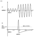
- FIG. 14 is a diagram illustrating an example of an output waveform of the 180 ° addition filter.
- FIG. 14A shows an example of the waveform of the input current signal. A failure has occurred in the power system at around 0.185 seconds.
- FIG. 14B is a diagram showing an output signal waveform of the 180 ° addition filter with respect to the input signal waveform of FIG. As shown in FIG. 14B, since the input signal waveform changes greatly before and after the failure detection, an output exceeding the detection threshold Th1 is obtained.
- Embodiment 3 In the third embodiment, another setting method of the coefficients k1 and k2 in the coefficient calculation unit 90 will be described.
- FIG. 15 is a diagram illustrating an example of setting the coefficient values k1 and k2 in the third embodiment.
- the coefficient values k1 and k2 are shown in a table format
- the coefficient values k1 and k2 are shown in a graph.
- the coefficient setting unit 93 in FIG. 3 rapidly decreases the coefficient k1 to 0.1 when 1T has elapsed since the failure was detected in the power system, and sets the coefficient k2 to 0.9. Increase rapidly. Thereafter, with the passage of time, the coefficient k1 is gradually increased and the coefficient k2 is gradually decreased. As shown in FIG. 15B, in the case of Embodiment 3, k1 and k2 change linearly.
- FIG. 16 is a diagram illustrating an amplitude value calculation result of the filter output signal waveform with respect to the input signal waveform of FIG. 9 in the setting of the coefficient values k1 and k2 illustrated in FIG.
- the amplitude value DF (t) long of the output signal of the first filter 81 is indicated by a thick broken line
- the amplitude value DF (t) short of the output signal of the second filter 82 is indicated by a thin broken line
- the coefficient calculation unit 90 The output signal amplitude value (k1 * DF (t) long + k2 * DF (t) short ) is indicated by a solid line.
- FIG. 16 When FIG. 16 is compared with FIG. 11, the response performance to the input signal is comparable, but in the case of FIG. 16, the output signal overshoots. However, the magnitude of the overshoot and the period in which the overshoot occurs can be reduced as compared with the case where the second filter 82 (60 ° difference filter) is used alone.
- this period is referred to as a verification period.
- the overshoot period can be made shorter than before, the above-described verification period can be shortened. As a result, a protection relay capable of high speed operation can be provided.
- Embodiment 4 FIG. In the fourth embodiment, another method for setting the coefficients k1 and k2 in the coefficient calculation unit 90 will be described.
- FIG. 17 is a diagram illustrating a setting example of coefficient values k1 and k2 in the fourth embodiment.
- coefficient values k1 and k2 are shown in a table format
- coefficient values k1 and k2 are shown in a graph.
- the coefficient setting unit 93 in FIG. 3 decreases the coefficient k1 rapidly to 0 and increases the coefficient k2 rapidly to 1 when 1T has elapsed since the failure was detected in the power system. Let Thereafter, this coefficient value is maintained for 2T (T is a relay operation cycle). Thereafter, the coefficient setting unit 93 gradually increases the coefficient k1 and gradually decreases the coefficient k2 over time. As shown in FIG. 17B, in the case of Embodiment 3, k1 and k2 change linearly.
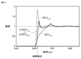
- FIG. 18 is a diagram illustrating the amplitude value calculation result of the filter output signal waveform with respect to the input signal waveform of FIG. 9 in the setting of the coefficient values k1 and k2 illustrated in FIG.
- the amplitude value DF (t) long of the output signal of the first filter 81 is indicated by a thick broken line
- the amplitude value DF (t) short of the output signal of the second filter 82 is indicated by a thin broken line
- the coefficient calculation unit 90 The output signal amplitude value (k1 * DF (t) long + k2 * DF (t) short ) is indicated by a solid line.
- the response to the input signal is slightly improved in the case of FIG. 18, but the overshoot of the output signal is larger.
- the magnitude of the overshoot and the period in which the overshoot occurs can be reduced as compared with the case where the second filter 82 (60 ° difference filter) is used alone. Therefore, the above-described verification period can be made shorter than before, and thus a protection relay capable of operating at a higher speed than before can be provided.
- FIG. The fifth embodiment is a modification of the first embodiment.
- the phase of the output signal of the first filter 81 and the phase of the output signal of the second filter 82 are the same or different from each other by 180 ° with respect to the fundamental frequency.
- the technique of the present disclosure can also be applied to a relay calculation using an instantaneous value such as a distance relay.
- FIG. 19 is a functional block diagram illustrating digital processing realized by the arithmetic circuit of FIG. 2 in the protection relay of the fifth embodiment. It is a functional block diagram which shows the digital processing content of CPU.
- the coefficient calculation unit 90 multiplies the output signal df (t) long of the first filter 81 by the coefficient k1, multiplies the output signal df (t) short of the second filter 82 by the coefficient k2, and these multiplication results. Are added to each other.
- the digital processing unit 80A of FIG. 19 is different from the digital processing unit 80 of FIG. 3 in that it further includes an amplitude value calculation unit 88 provided between the coefficient calculation unit 90 and the operation determination unit 95.
- the amplitude value calculation unit 88 obtains the amplitude value of the output signal (k1 * df (t) long + k2 * df (t) short ) of the coefficient calculation unit 90.
- the operation determination unit 95 performs operation determination based on the amplitude value calculated by the amplitude value calculation unit 88.
- the amplitude value calculation unit 88 needs to be provided when an amplitude value calculation is necessary for operation determination like an overcurrent relay, but is not necessary for a distance relay that performs operation determination using instantaneous values. It is.
- the operation determination unit 95 performs the operation determination based on the output signal (k1 * df (t) long + k2 * df (t) short ) of the coefficient calculation unit 90.
- FIG. 20 is a flowchart showing a processing procedure of the digital processing unit of FIG.
- the flowchart in FIG. 20 shows the operation of the digital processing unit in FIG. 19 in chronological order.
- Each step in FIG. 20 is executed by the CPU 61 in FIG.
- the CPU 61 takes out data necessary for the filter calculation from the RAM 62.
- time-series current data and / or voltage data detected from the power system and subjected to A / D conversion are stored in the RAM 62.
- the CPU 61 performs a filter operation using the read data as the first filter 81, the second filter 82, and the third filter 83 described above.
- the first filter 81 and the second filter 82 are FIR filters that remove DC components. Further, the first filter 81 and the second filter 82 have a feature that the window length of the first filter 81 is longer than the window length of the second filter 82 filter. Both the first filter 81 and the second filter 82 pass at least a part of the fundamental wave component, but the second filter 82 having a shorter window length has a larger attenuation of the fundamental wave component and a higher content ratio of the harmonic component. .
- the third filter 83 is an FIR filter that removes the fundamental wave component.
- the CPU 61 determines whether or not a failure has occurred in the power system based on the output of the third filter 83. For example, when the state where the output level of the third filter 83 exceeds a preset threshold value continues for a predetermined verification period (for example, 2T), the CPU 61 causes a failure in the power system. It is determined that
- step S250 the CPU 61 uses the initially set values of the coefficients k1 and k2, and then uses the first filter 81. Output signal df (t) long is multiplied by a coefficient k1, and the output signal df (t) short of the second filter 82 is multiplied by a coefficient k2. The CPU 61 adds these multiplication results to each other (when the phase difference is 0 °). When the phase difference is 180 °, the CPU 61 subtracts these multiplication results from each other.
- the CPU 61 calculates the amplitude value of the calculated signal (k1 * df (t) long + k2 * df (t) short ). Any known method may be used as an amplitude value calculation method, and is not particularly limited.
- step S270 the CPU 61 performs an operation determination based on the result of the amplitude value calculation.
- the amplitude value calculation result is almost determined by the output of the first filter 81, it is possible to prevent the overcurrent relay from making an erroneous determination due to a sudden surge current or the like. Thereafter, the procedure from step S210 is repeated.
- the CPU 61 sets the coefficients k1 and k2 based on a preset table or mathematical expression as time elapses from the failure detection time.
- the CPU 61 calculates k1 * df (t) long + k2 * df (t) short using the values of the coefficients k1 and k2 changed in step S240.
- the CPU 61 calculates the amplitude value of the output signal (k1 * df (t) long + k2 * df (t) short ) of the coefficient calculation unit 90.
- the CPU 61 performs an operation determination based on the output result of the amplitude value calculation. For example, in the case of an overcurrent relay, if the result of the amplitude value calculation exceeds the threshold value, the CPU 61 sets the operation flag to 1 to open the circuit breaker.
- step S260 need not be executed.
- the condition that the phase of the output signal of the first filter 81 and the phase of the output signal of the second filter 82 are equal or different from each other by 180 ° with respect to the fundamental frequency. Is added.
- the instantaneous values of the output signals of the respective filters are synthesized (added in the case of in-phase and subtracted in the case of reverse phase) without obtaining the amplitude values of the output signals of the first filter 81 and the second filter 82. It is possible.
- the protection relay of the fifth embodiment can be realized.
- at least one of the first filter 81 and the second filter 82 includes a phase shifter that changes the phase of the time-series data obtained as a filter calculation result.
- the operation delay can be further reduced.
- the technology of the present disclosure can also be applied to a relay calculation that uses an instantaneous value such as a distance relay.
- Embodiment 6 FIG. In the sixth embodiment, a specific example of the first filter 81 described in the fifth embodiment will be described.
- a 60 ° difference filter can be used as a specific configuration of the second filter 82, and a 180 ° addition filter can be used as a specific configuration of the third filter 83. Since these filter characteristics have been described in the second embodiment, description thereof will not be repeated. Further, as the values of the coefficients k1 and k2, the setting values shown in FIG. 15 described in the third embodiment are used.
- the first filter 81 is configured by connecting a plurality of addition filters and a difference filter in series. Specifically, when the current input signal is i (t), the following filters (a) to (f) are connected in series.
- the relay calculation period T is 30 ° in electrical angle.
- the input signal i (t) is input to the 30 ° addition filter represented by Expression (6A).
- the output i 1 (t) of the 30 ° addition filter represented by Expression (6A) is input to the 30 ° difference filter represented by Expression (6B).
- the output i 2 (t) of the 30 ° difference filter represented by Expression (6B) is input to the 60 ° addition filter represented by Expression (6C). Thereafter, the same calculation is performed, and finally an output signal i 6 (t) is obtained with respect to the input signal i (t).
- the phase advance with respect to the fundamental frequency is 60 °, which is the same as the 60 ° difference filter constituting the second filter 82.
- the window length of the first filter 81 is 390 ° in electrical angle, and is longer than the window length of the second filter 82 (60 ° in electrical angle).
- Simulation result A simulation result when using the first filter 81 will be described.
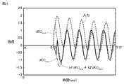
- FIG. 21 is a diagram illustrating a filter output waveform with respect to the input signal waveform of FIG. 9 in the protection relay of the fifth embodiment.
- the input signal is indicated by a thick broken line
- the output signal df (t) long of the first filter 81 is indicated by a two-dot chain line
- the output signal df (t) short of the second filter 82 is indicated by a thin broken line.
- the output signal (k1 * df (t) long + k2 * df (t) short ) of the coefficient calculation unit 90 is indicated by a solid line.
- the output signal df (t) long of the first filter 81, the output signal df (t) short of the second filter 82, and the output signal of the coefficient calculation unit 90 may be in phase with each other. Recognize.
- FIG. 22 is a diagram showing the calculation result of the amplitude value based on the filter output waveform of FIG.
- the amplitude value of the output signal (k1 * df (t) long + k2 * df (t) short ) of the coefficient calculation unit 90 (that is, the output signal of the amplitude value calculation unit 88) is indicated by a solid line.
- the amplitude value DF (t) long of the output signal df (t) long of the first filter 81 and the amplitude value DF (t) short of the output signal df (t) short of the second filter 82 are used. It also shows.
- protection relay 51 analog input circuit, 57 A / D converter, 60 arithmetic circuit, 61 CPU, 62 RAM, 63 ROM, 64 memory, 71 digital input circuit, 72 digital output circuit, 79 time series data, 80, 80A Digital processing unit, 81 1st filter, 82 2nd filter, 83 3rd filter, 84, 85, 88 amplitude value calculation unit, 86 failure determination unit, 90 coefficient calculation unit, 91, 92 multiplier, 93 coefficient setting unit, 94 adder, 95 operation determination unit, T relay operation cycle, k1 first coefficient, k2 second coefficient.
Landscapes
- Physics & Mathematics (AREA)
- General Physics & Mathematics (AREA)
- Emergency Protection Circuit Devices (AREA)
Abstract
Description
[電力系統の構成例]
図1は、保護リレーを備えた電力系統の構成例を示す図である。図1を参照して、送電線40の一端には電源42が設けられる。なお、送電線40は三相送電線であるが図1では図解を容易にするために1本の線で示している。
図2は、図1の保護リレーのハードウェア構成の一例を示すブロック図である。図2の保護リレー50は、いわゆるデジタルリレー装置と同様の構成を有している。具体的に図2を参照して、保護リレー50は、アナログ入力回路51と、演算回路60と、I/O(Input and Output)回路70とを備える。
次に、演算回路60で実現されるデジタル処理の内容について詳しく説明する。以下の機能は、CPU61がプログラムに従って動作することによって実現されるものとして説明するが、前述のように、演算回路60は、ASICまたはFPGAなどによって実現されていてもよい。また、以下では、主として過電流リレーを例に挙げて説明するが、本開示は過電流リレーに限定されるものではない。
I2=[i(t-1)・i(t-2)-i(t)・i(t-3)]/[sin30°・sin60°] …(1)
で求めることができる。より、一般的な表式は上記の特許文献3に開示されている。
図5は、図2の演算回路による処理手順を示すフローチャートである。図5のフローチャートは、図3および図4のデジタル処理部の動作を時系列順に示したものである。図5の各ステップは、図2のCPU61によって実行される。
以上のとおり、実施の形態1の保護リレーによれば、互いに窓長の異なる第1フィルタ81および第2フィルタ82を利用し、第1フィルタ81の出力信号のk1倍と第2フィルタ82の出力信号のk2倍との和に基づいて動作判定が行われる。電力系統に故障が検出されたときには、前記第1係数を減少させかつ前記第2係数を増加させ、その後、時間の経過とともに前記第1係数および前記第2係数を変化させるようにする。これにより、オーバーシュートの発生を抑制することができ、応答速度と動作判定精度とを両立することが可能な保護リレーを提供することができる。
実施の形態2では、実施の形態1で説明した第1フィルタ81、第2フィルタ82、おおよび第3フィルタ83の具体例と、係数k1,k2の具体的な設定方法について説明する。
(第1フィルタ81)
具体的に、第1フィルタ81としてフル・サイクル・コサイン・フィルタ(Full Cycle Cosine Filter)が用いられる。リレー演算周期Tを電気角で30°としたとき、フル・サイクル・コサイン・フィルタは、
i(t)+i(t-1)・cos30°+i(t-2)・cos60°+i(t-3)・cos90°+i(t-4)・cos120°
+i(t-5)・cos150°+i(t-6)・cos180°+i(t-7)・cos210°+i(t-8)・cos240°
+i(t-9)・cos270°+i(t-10)・cos300°+i(t-11)・cos330° …(2)
のように表される。したがって、フル・サイクル・コサイン・フィルタの窓長は電気角で330°である。
第2フィルタ82として、60°差分フィルタが用いられる。60°差分フィルタは、
i(t)-i(t-2) …(3)
で表される。ただし、リレー演算周期Tを電気角で30°としている。したがって、60°差分フィルタの窓長は電気角で60°である。
図8は、実施の形態2における係数値k1,k2の設定例を示す図である。図8(A)では係数値k1,k2を表形式で示し、図8(B)では数値k1,k2をグラフで示す。図8(A)では、電力系統の故障検出後の経過時間がリレー演算周期T(Tは電気角で30°に対応する)を基準にして示されている。すなわち、故障検出から1Tの時間が経過した以降において係数値k1,k2が変化する。
i(t)=0 ただし、0≦t<0.05(秒) …(4A)
i(t)=sin(ωt)+exp(-t/τ) ただし、t≧0.05(秒)
…(4B)
によって表される。時刻t=0.05(秒)において、1相地絡などの単純故障が生じたと仮定している。系統周波数fを50Hzとし、リレー演算周期Tを1.667msec(対応する電気角を30°)とする。
次に、第3フィルタ83について説明する。第3フィルタ83として180°加算フィルタが用いられる。180°加算フィルタは、
i(t)+i(t-6) …(5)
で表される。ただし、リレー演算周期Tを電気角で30°としている。したがって、180°加算フィルタの窓長は電気角で180°である。
実施の形態2では、実施の形態1で説明した第1フィルタ81、第2フィルタ82、および第3フィルタ83の具体例と、係数k1,k2の具体的な設定方法について説明した。実施の形態1の場合と同様に、オーバーシュートの発生を抑制することができ、応答速度と動作判定精度とを両立することが可能な保護リレーを提供することができる。
実施の形態3では、係数演算部90における係数k1,k2の他の設定方法について説明する。
実施の形態4では、係数演算部90における係数k1,k2のさらに他の設定方法について説明する。
実施の形態5は、実施の形態1を変形したものである。実施の形態5では、基本波周波数に対して、第1フィルタ81の出力信号の位相と第2フィルタ82の出力信号の位相とが、同じか互いに180°異なる場合について説明する。この場合、第1フィルタ81および第2フィルタ82の各々の出力信号の振幅値を求めずに、各フィルタの出力信号の瞬時値を合成(加算または減算)することが可能である。この結果、動作遅れをより少なくすることができる。さらに、距離リレーなど瞬時値を用いるリレー演算にも、本開示の技術を適用することが可能になる。以下、図面を参照して詳しく説明する。
その次のステップS230において、CPU61は、第3フィルタ83の出力に基づいて電力系統で故障が発生しているか否かを判定する。たとえば、CPU61は、第3フィルタ83の出力の大きさが予め設定された閾値を超えた状態が、予め定められた照合期間(たとえば、2T)の間継続したときに、電力系統で故障が発生したと判定する。
実施の形態6では、実施の形態5で説明した第1フィルタ81の具体例について説明する。なお、第2フィルタ82の具体的構成として60°差分フィルタを用いることができ、第3フィルタ83の具体的構成として180°加算フィルタを用いることができる。これらフィルタ特性は実施の形態2で説明したので、説明を繰り返さない。また、係数k1,k2の値として、実施の形態3で説明した図15の設定値が用いられる。
第1フィルタ81は、複数の加算フィルタと差分フィルタとを直列に接続することによって構成される。具体的に、現時点の入力信号をi(t)としたとき以下のフィルタ(a)~(f)が直列に接続される。なお、リレー演算周期Tは電気角で30°とする。
(b) i2(t)=i1(t)-i1(t-1) …(6B)
(c) i3(t)=i2(t)+i2(t-2) …(6C)
(d) i4(t)=i3(t)+i3(t-3) …(6D)
(e) i5(t)=i4(t)+√(3)*i4(t-1)+i4(t-2) …(6E)
(f) i6(t)=-i5(t)-i5(t-4) …(6F)
上式において、入力信号i(t)は式(6A)で表される30°加算フィルタに入力される。次に、式(6A)で表される30°加算フィルタの出力i1(t)は式(6B)で表される30°差分フィルタに入力される。次に、式(6B)で表される30°差分フィルタの出力i2(t)は、式(6C)で表される60°加算フィルタに入力される。以下同様の演算が行われ、最終的に入力信号i(t)に対して出力信号i6(t)が得られる。
上記の第1フィルタ81を用いた場合のシミュレーション結果について説明する。
Claims (12)
- 電力系統の電流または電圧を表す信号を検出してA/D(Analog to Digital)変換することにより、時系列データを生成するアナログ入力回路と、
前記時系列データに基づいたデジタル処理を行う演算回路とを備え、
前記演算回路は、
前記時系列データのうち直流成分および電力系統の少なくとも一部の次数の高調波成分を減衰または除去して前記電力系統の基本波成分の少なくとも一部を通過させ、第1の窓長を有する第1フィルタと、
前記時系列データのうち直流成分および電力系統の少なくとも一部の次数の高調波成分を減衰または除去して前記基本波成分の少なくとも一部を通過させ、前記第1の窓長より短い第2の窓長を有する第2フィルタと、
前記第1フィルタの出力信号に基づく値に第1係数を乗算し、前記第2フィルタの出力信号に基づく値に第2係数を乗算し、乗算結果を合成する係数演算部と、
前記係数演算部による合成結果に基づいて動作判定を行う動作判定部と、
前記第1係数および前記第2係数を設定する係数設定部とを含み、
前記係数設定部は、前記電力系統の故障が検出されたときに、前記第1係数を減少させかつ前記第2係数を増加させ、その後、時間経過とともに前記第1係数および前記第2係数を変化させる、保護リレー。 - 前記演算回路は、さらに、
前記時系列データのうち基本波成分を除去する第3フィルタと、
前記第3フィルタの出力信号に基づいて前記電力系統の故障を検出する故障判定部とを含む、請求項1に記載の保護リレー。 - 前記第1フィルタは、フル・サイクル・コサイン・フィルタを含み、
前記第2フィルタは、60°差分フィルタを含み、
前記第3フィルタは、180°加算フィルタを含む、請求項2に記載の保護リレー。 - 前記演算回路は、さらに、
前記第1フィルタの出力信号の振幅を計算する第1振幅値演算部と、
前記第2フィルタの出力信号の振幅を計算する第2振幅値演算部とを含み、
前記係数演算部は、前記第1振幅値演算部によって算出された振幅値に前記第1係数を乗算し、前記第2振幅値演算部によって算出された振幅値に前記第2係数を乗算する、請求項1~3のいずれか1項に記載の保護リレー。 - 前記基本波成分の周波数に対して、前記第1フィルタの出力信号の位相と前記第2フィルタの出力信号の位相とは同じであるか、互いに180°異なり、
前記係数演算部は、前記第1フィルタの出力信号に前記第1係数を乗算し、前記第2フィルタの出力信号に前記第2係数を乗算し、乗算結果を合成し、
前記動作判定部は、前記係数演算部による前記合成結果に基づいて動作判定を行う、請求項1~3のいずれか1項に記載の保護リレー。 - 前記係数設定部は、前記第1係数および前記第2係数と故障検出後の経過時間との間の予め決定された対応関係に基づいて、前記第1係数および前記第2係数を設定する、請求項1~5のいずれか1項に記載の保護リレー。
- 前記係数設定部は、前記電力系統の故障が検出されたときに、前記第1係数を減少させかつ前記第2係数を増加させ、その後、前記第1係数を増加させかつ前記第2係数を減少させた後に、再び前記第1係数を減少させかつ前記第2係数を増加させ、その後、前記第1係数を増加させかつ前記第2係数を減少させる、請求項1~6のいずれか1項に記載の保護リレー。
- 前記係数設定部は、前記電力系統の故障が検出されたときに、前記第1係数を減少させかつ前記第2係数を増加させ、その後、時間の経過とともに前記第1係数を徐々に増加させかつ前記第2係数を徐々に減少させる、請求項1~6のいずれか1項に記載の保護リレー。
- 前記係数設定部は、前記電力系統の故障が検出されたときに、前記第1係数を0に設定しかつ前記第2係数を1に設定する、請求項8に記載の保護リレー。
- 前記係数設定部は、前記電力系統の故障が検出されたときに、前記第1係数を0に設定しかつ前記第2係数を1に設定してからその状態を維持した後に、時間の経過とともに前記第1係数を徐々に増加させかつ前記第2係数を徐々に減少させる請求項1~6のいずれか1項に記載の保護リレー。
- 前記第1係数と前記第2係数との和は1に等しい、請求項1~10のいずれか1項に記載の保護リレー。
- 前記対応関係は、故障時における前記電力系統の直流電流成分が最大となるような仮想の前記時系列データに基づいて、前記電力系統の故障検出後に前記合成結果の振幅が入力信号の振幅に等しくなるように決定される、請求項6に記載の保護リレー。
Priority Applications (4)
| Application Number | Priority Date | Filing Date | Title |
|---|---|---|---|
| GB2013118.1A GB2585533B (en) | 2018-04-25 | 2018-04-25 | Protection relay |
| US16/975,902 US11355915B2 (en) | 2018-04-25 | 2018-04-25 | Protection relay |
| PCT/JP2018/016757 WO2019207673A1 (ja) | 2018-04-25 | 2018-04-25 | 保護リレー |
| JP2018537886A JP6400263B1 (ja) | 2018-04-25 | 2018-04-25 | 保護リレー |
Applications Claiming Priority (1)
| Application Number | Priority Date | Filing Date | Title |
|---|---|---|---|
| PCT/JP2018/016757 WO2019207673A1 (ja) | 2018-04-25 | 2018-04-25 | 保護リレー |
Publications (1)
| Publication Number | Publication Date |
|---|---|
| WO2019207673A1 true WO2019207673A1 (ja) | 2019-10-31 |
Family
ID=63708684
Family Applications (1)
| Application Number | Title | Priority Date | Filing Date |
|---|---|---|---|
| PCT/JP2018/016757 Ceased WO2019207673A1 (ja) | 2018-04-25 | 2018-04-25 | 保護リレー |
Country Status (4)
| Country | Link |
|---|---|
| US (1) | US11355915B2 (ja) |
| JP (1) | JP6400263B1 (ja) |
| GB (1) | GB2585533B (ja) |
| WO (1) | WO2019207673A1 (ja) |
Cited By (1)
| Publication number | Priority date | Publication date | Assignee | Title |
|---|---|---|---|---|
| JP2024115809A (ja) * | 2023-02-15 | 2024-08-27 | 三菱電機株式会社 | 保護リレー装置 |
Families Citing this family (3)
| Publication number | Priority date | Publication date | Assignee | Title |
|---|---|---|---|---|
| JP2022187735A (ja) * | 2021-06-08 | 2022-12-20 | 東京エレクトロン株式会社 | 異常検出方法及び異常検出装置 |
| KR102782405B1 (ko) * | 2022-04-25 | 2025-03-19 | 코츠테크놀로지주식회사 | 전류 비율 차동 계전기 및 그의 동작 방법 |
| CN115912249B (zh) * | 2023-01-10 | 2026-03-20 | 广东电网有限责任公司 | 一种电力系统继电保护方法、装置、存储介质以及系统 |
Citations (4)
| Publication number | Priority date | Publication date | Assignee | Title |
|---|---|---|---|---|
| JPS60204219A (ja) * | 1984-03-29 | 1985-10-15 | 株式会社東芝 | デイジタル故障点標定装置 |
| JP2004048855A (ja) * | 2002-07-09 | 2004-02-12 | Toshiba Corp | 距離継電装置 |
| JP2007014052A (ja) * | 2005-06-28 | 2007-01-18 | Mitsubishi Electric Corp | デジタル保護継電装置 |
| JP2011250518A (ja) * | 2010-05-24 | 2011-12-08 | Mitsubishi Electric Corp | 過電流継電器 |
Family Cites Families (5)
| Publication number | Priority date | Publication date | Assignee | Title |
|---|---|---|---|---|
| US4073008A (en) * | 1975-08-29 | 1978-02-07 | Tokyo Shibaura Denki Kabushiki Kaisha | Apparatus for calculating amplitude values |
| JPH0812222B2 (ja) * | 1985-11-08 | 1996-02-07 | 株式会社東芝 | ディジタル故障点標定装置 |
| JP2648325B2 (ja) | 1988-03-08 | 1997-08-27 | 三菱電機株式会社 | 演算形ディジタル継電器 |
| JP2765907B2 (ja) * | 1989-01-20 | 1998-06-18 | 株式会社日立製作所 | 変圧器故障検出方法およびその装置 |
| JP2001250518A (ja) * | 2000-03-07 | 2001-09-14 | Yuasa Corp | 密閉形電池 |
-
2018
- 2018-04-25 WO PCT/JP2018/016757 patent/WO2019207673A1/ja not_active Ceased
- 2018-04-25 US US16/975,902 patent/US11355915B2/en active Active
- 2018-04-25 GB GB2013118.1A patent/GB2585533B/en not_active Expired - Fee Related
- 2018-04-25 JP JP2018537886A patent/JP6400263B1/ja active Active
Patent Citations (4)
| Publication number | Priority date | Publication date | Assignee | Title |
|---|---|---|---|---|
| JPS60204219A (ja) * | 1984-03-29 | 1985-10-15 | 株式会社東芝 | デイジタル故障点標定装置 |
| JP2004048855A (ja) * | 2002-07-09 | 2004-02-12 | Toshiba Corp | 距離継電装置 |
| JP2007014052A (ja) * | 2005-06-28 | 2007-01-18 | Mitsubishi Electric Corp | デジタル保護継電装置 |
| JP2011250518A (ja) * | 2010-05-24 | 2011-12-08 | Mitsubishi Electric Corp | 過電流継電器 |
Cited By (1)
| Publication number | Priority date | Publication date | Assignee | Title |
|---|---|---|---|---|
| JP2024115809A (ja) * | 2023-02-15 | 2024-08-27 | 三菱電機株式会社 | 保護リレー装置 |
Also Published As
| Publication number | Publication date |
|---|---|
| US20210006059A1 (en) | 2021-01-07 |
| GB2585533B (en) | 2022-06-08 |
| JP6400263B1 (ja) | 2018-10-03 |
| GB2585533A (en) | 2021-01-13 |
| US11355915B2 (en) | 2022-06-07 |
| JPWO2019207673A1 (ja) | 2020-04-30 |
| GB202013118D0 (en) | 2020-10-07 |
Similar Documents
| Publication | Publication Date | Title |
|---|---|---|
| JP6400263B1 (ja) | 保護リレー | |
| Ferrer et al. | Fourier and Walsh digital filtering algorithms for distance protection | |
| US10393810B2 (en) | Method for identifying the fault by current differential protection and device thereof | |
| JPS62110168A (ja) | デイジタル故障点標定装置 | |
| CN121385500A (zh) | 一种煤矿高压开关谐波干扰剔除方法及滤波监控保护装置 | |
| JP6887906B2 (ja) | 零相電流差動リレー | |
| Silva et al. | On combining wavelet-based designed filters and an adaptive mimic filter for phasor estimation in digital relaying | |
| JP6230489B2 (ja) | デジタル保護リレー装置 | |
| JP5298562B2 (ja) | ディジタル形保護リレー | |
| Hossain et al. | Design and testing of a bus differential protection scheme using partial operating current (POC) algorithm | |
| JP5664166B2 (ja) | 電流差動保護継電装置 | |
| JP5029357B2 (ja) | 適応ディジタルフィルタ、信号処理方法、fm受信機およびプログラム | |
| WO2005078886A1 (fr) | Procede de restriction de courant homopolaire pour la protection differentielle de transformateur d'energie | |
| CN111781453B (zh) | 一种基于故障时刻的直流系统换相失败风险评估方法 | |
| Nam et al. | Modified notch filter-based instantaneous phasor estimation for high-speed distance protection | |
| JP2012005060A (ja) | 雑音除去装置 | |
| JPS6022772Y2 (ja) | デイジタル保護継電装置 | |
| JP2020188639A (ja) | 過電流保護リレー | |
| Kezunovic et al. | Modeling of digital relay and power system signals | |
| JP2011130536A (ja) | 三相過電流保護リレー | |
| JPS6011722Y2 (ja) | デイジタル保護継電装置 | |
| JP6399974B2 (ja) | 保護リレー装置 | |
| Ibarra et al. | Benchmarking Online Electric Power Computation Techniques in Non-Sinusoidal Environments | |
| JP6253515B2 (ja) | ディジタル保護リレー装置 | |
| JP5289071B2 (ja) | 過電流継電装置 |
Legal Events
| Date | Code | Title | Description |
|---|---|---|---|
| ENP | Entry into the national phase |
Ref document number: 2018537886 Country of ref document: JP Kind code of ref document: A |
|
| 121 | Ep: the epo has been informed by wipo that ep was designated in this application |
Ref document number: 18916632 Country of ref document: EP Kind code of ref document: A1 |
|
| ENP | Entry into the national phase |
Ref document number: 202013118 Country of ref document: GB Kind code of ref document: A Free format text: PCT FILING DATE = 20180425 |
|
| NENP | Non-entry into the national phase |
Ref country code: DE |
|
| 122 | Ep: pct application non-entry in european phase |
Ref document number: 18916632 Country of ref document: EP Kind code of ref document: A1 |