WO2019203266A1 - Feuille d'isolation, stratifié et substrat - Google Patents
Feuille d'isolation, stratifié et substrat Download PDFInfo
- Publication number
- WO2019203266A1 WO2019203266A1 PCT/JP2019/016454 JP2019016454W WO2019203266A1 WO 2019203266 A1 WO2019203266 A1 WO 2019203266A1 JP 2019016454 W JP2019016454 W JP 2019016454W WO 2019203266 A1 WO2019203266 A1 WO 2019203266A1
- Authority
- WO
- WIPO (PCT)
- Prior art keywords
- resin composition
- composition layer
- inorganic particles
- insulating sheet
- plate
- Prior art date
Links
Images


Classifications
-
- H—ELECTRICITY
- H05—ELECTRIC TECHNIQUES NOT OTHERWISE PROVIDED FOR
- H05K—PRINTED CIRCUITS; CASINGS OR CONSTRUCTIONAL DETAILS OF ELECTRIC APPARATUS; MANUFACTURE OF ASSEMBLAGES OF ELECTRICAL COMPONENTS
- H05K1/00—Printed circuits
- H05K1/02—Details
- H05K1/03—Use of materials for the substrate
- H05K1/05—Insulated conductive substrates, e.g. insulated metal substrate
- H05K1/056—Insulated conductive substrates, e.g. insulated metal substrate the metal substrate being covered by an organic insulating layer
-
- B—PERFORMING OPERATIONS; TRANSPORTING
- B32—LAYERED PRODUCTS
- B32B—LAYERED PRODUCTS, i.e. PRODUCTS BUILT-UP OF STRATA OF FLAT OR NON-FLAT, e.g. CELLULAR OR HONEYCOMB, FORM
- B32B15/00—Layered products comprising a layer of metal
- B32B15/04—Layered products comprising a layer of metal comprising metal as the main or only constituent of a layer, which is next to another layer of the same or of a different material
- B32B15/08—Layered products comprising a layer of metal comprising metal as the main or only constituent of a layer, which is next to another layer of the same or of a different material of synthetic resin
- B32B15/092—Layered products comprising a layer of metal comprising metal as the main or only constituent of a layer, which is next to another layer of the same or of a different material of synthetic resin comprising epoxy resins
-
- B—PERFORMING OPERATIONS; TRANSPORTING
- B32—LAYERED PRODUCTS
- B32B—LAYERED PRODUCTS, i.e. PRODUCTS BUILT-UP OF STRATA OF FLAT OR NON-FLAT, e.g. CELLULAR OR HONEYCOMB, FORM
- B32B27/00—Layered products comprising a layer of synthetic resin
-
- B—PERFORMING OPERATIONS; TRANSPORTING
- B32—LAYERED PRODUCTS
- B32B—LAYERED PRODUCTS, i.e. PRODUCTS BUILT-UP OF STRATA OF FLAT OR NON-FLAT, e.g. CELLULAR OR HONEYCOMB, FORM
- B32B27/00—Layered products comprising a layer of synthetic resin
- B32B27/06—Layered products comprising a layer of synthetic resin as the main or only constituent of a layer, which is next to another layer of the same or of a different material
- B32B27/08—Layered products comprising a layer of synthetic resin as the main or only constituent of a layer, which is next to another layer of the same or of a different material of synthetic resin
-
- B—PERFORMING OPERATIONS; TRANSPORTING
- B32—LAYERED PRODUCTS
- B32B—LAYERED PRODUCTS, i.e. PRODUCTS BUILT-UP OF STRATA OF FLAT OR NON-FLAT, e.g. CELLULAR OR HONEYCOMB, FORM
- B32B27/00—Layered products comprising a layer of synthetic resin
- B32B27/18—Layered products comprising a layer of synthetic resin characterised by the use of special additives
- B32B27/20—Layered products comprising a layer of synthetic resin characterised by the use of special additives using fillers, pigments, thixotroping agents
-
- B—PERFORMING OPERATIONS; TRANSPORTING
- B32—LAYERED PRODUCTS
- B32B—LAYERED PRODUCTS, i.e. PRODUCTS BUILT-UP OF STRATA OF FLAT OR NON-FLAT, e.g. CELLULAR OR HONEYCOMB, FORM
- B32B27/00—Layered products comprising a layer of synthetic resin
- B32B27/38—Layered products comprising a layer of synthetic resin comprising epoxy resins
-
- C—CHEMISTRY; METALLURGY
- C08—ORGANIC MACROMOLECULAR COMPOUNDS; THEIR PREPARATION OR CHEMICAL WORKING-UP; COMPOSITIONS BASED THEREON
- C08K—Use of inorganic or non-macromolecular organic substances as compounding ingredients
- C08K13/00—Use of mixtures of ingredients not covered by one single of the preceding main groups, each of these compounds being essential
- C08K13/04—Ingredients characterised by their shape and organic or inorganic ingredients
-
- C—CHEMISTRY; METALLURGY
- C08—ORGANIC MACROMOLECULAR COMPOUNDS; THEIR PREPARATION OR CHEMICAL WORKING-UP; COMPOSITIONS BASED THEREON
- C08K—Use of inorganic or non-macromolecular organic substances as compounding ingredients
- C08K3/00—Use of inorganic substances as compounding ingredients
-
- C—CHEMISTRY; METALLURGY
- C08—ORGANIC MACROMOLECULAR COMPOUNDS; THEIR PREPARATION OR CHEMICAL WORKING-UP; COMPOSITIONS BASED THEREON
- C08K—Use of inorganic or non-macromolecular organic substances as compounding ingredients
- C08K3/00—Use of inorganic substances as compounding ingredients
- C08K3/28—Nitrogen-containing compounds
-
- C—CHEMISTRY; METALLURGY
- C08—ORGANIC MACROMOLECULAR COMPOUNDS; THEIR PREPARATION OR CHEMICAL WORKING-UP; COMPOSITIONS BASED THEREON
- C08K—Use of inorganic or non-macromolecular organic substances as compounding ingredients
- C08K3/00—Use of inorganic substances as compounding ingredients
- C08K3/38—Boron-containing compounds
-
- C—CHEMISTRY; METALLURGY
- C08—ORGANIC MACROMOLECULAR COMPOUNDS; THEIR PREPARATION OR CHEMICAL WORKING-UP; COMPOSITIONS BASED THEREON
- C08K—Use of inorganic or non-macromolecular organic substances as compounding ingredients
- C08K7/00—Use of ingredients characterised by shape
-
- C—CHEMISTRY; METALLURGY
- C08—ORGANIC MACROMOLECULAR COMPOUNDS; THEIR PREPARATION OR CHEMICAL WORKING-UP; COMPOSITIONS BASED THEREON
- C08L—COMPOSITIONS OF MACROMOLECULAR COMPOUNDS
- C08L63/00—Compositions of epoxy resins; Compositions of derivatives of epoxy resins
-
- H—ELECTRICITY
- H01—ELECTRIC ELEMENTS
- H01B—CABLES; CONDUCTORS; INSULATORS; SELECTION OF MATERIALS FOR THEIR CONDUCTIVE, INSULATING OR DIELECTRIC PROPERTIES
- H01B17/00—Insulators or insulating bodies characterised by their form
- H01B17/56—Insulating bodies
-
- H—ELECTRICITY
- H01—ELECTRIC ELEMENTS
- H01B—CABLES; CONDUCTORS; INSULATORS; SELECTION OF MATERIALS FOR THEIR CONDUCTIVE, INSULATING OR DIELECTRIC PROPERTIES
- H01B17/00—Insulators or insulating bodies characterised by their form
- H01B17/56—Insulating bodies
- H01B17/60—Composite insulating bodies
-
- H—ELECTRICITY
- H01—ELECTRIC ELEMENTS
- H01B—CABLES; CONDUCTORS; INSULATORS; SELECTION OF MATERIALS FOR THEIR CONDUCTIVE, INSULATING OR DIELECTRIC PROPERTIES
- H01B3/00—Insulators or insulating bodies characterised by the insulating materials; Selection of materials for their insulating or dielectric properties
- H01B3/18—Insulators or insulating bodies characterised by the insulating materials; Selection of materials for their insulating or dielectric properties mainly consisting of organic substances
- H01B3/30—Insulators or insulating bodies characterised by the insulating materials; Selection of materials for their insulating or dielectric properties mainly consisting of organic substances plastics; resins; waxes
- H01B3/40—Insulators or insulating bodies characterised by the insulating materials; Selection of materials for their insulating or dielectric properties mainly consisting of organic substances plastics; resins; waxes epoxy resins
-
- H—ELECTRICITY
- H05—ELECTRIC TECHNIQUES NOT OTHERWISE PROVIDED FOR
- H05K—PRINTED CIRCUITS; CASINGS OR CONSTRUCTIONAL DETAILS OF ELECTRIC APPARATUS; MANUFACTURE OF ASSEMBLAGES OF ELECTRICAL COMPONENTS
- H05K1/00—Printed circuits
- H05K1/02—Details
- H05K1/03—Use of materials for the substrate
-
- H—ELECTRICITY
- H05—ELECTRIC TECHNIQUES NOT OTHERWISE PROVIDED FOR
- H05K—PRINTED CIRCUITS; CASINGS OR CONSTRUCTIONAL DETAILS OF ELECTRIC APPARATUS; MANUFACTURE OF ASSEMBLAGES OF ELECTRICAL COMPONENTS
- H05K1/00—Printed circuits
- H05K1/02—Details
- H05K1/03—Use of materials for the substrate
- H05K1/0313—Organic insulating material
- H05K1/0353—Organic insulating material consisting of two or more materials, e.g. two or more polymers, polymer + filler, + reinforcement
- H05K1/036—Multilayers with layers of different types
-
- H—ELECTRICITY
- H05—ELECTRIC TECHNIQUES NOT OTHERWISE PROVIDED FOR
- H05K—PRINTED CIRCUITS; CASINGS OR CONSTRUCTIONAL DETAILS OF ELECTRIC APPARATUS; MANUFACTURE OF ASSEMBLAGES OF ELECTRICAL COMPONENTS
- H05K1/00—Printed circuits
- H05K1/02—Details
- H05K1/03—Use of materials for the substrate
- H05K1/0313—Organic insulating material
- H05K1/0353—Organic insulating material consisting of two or more materials, e.g. two or more polymers, polymer + filler, + reinforcement
- H05K1/0373—Organic insulating material consisting of two or more materials, e.g. two or more polymers, polymer + filler, + reinforcement containing additives, e.g. fillers
-
- B—PERFORMING OPERATIONS; TRANSPORTING
- B32—LAYERED PRODUCTS
- B32B—LAYERED PRODUCTS, i.e. PRODUCTS BUILT-UP OF STRATA OF FLAT OR NON-FLAT, e.g. CELLULAR OR HONEYCOMB, FORM
- B32B2250/00—Layers arrangement
- B32B2250/03—3 layers
-
- B—PERFORMING OPERATIONS; TRANSPORTING
- B32—LAYERED PRODUCTS
- B32B—LAYERED PRODUCTS, i.e. PRODUCTS BUILT-UP OF STRATA OF FLAT OR NON-FLAT, e.g. CELLULAR OR HONEYCOMB, FORM
- B32B2250/00—Layers arrangement
- B32B2250/04—4 layers
-
- B—PERFORMING OPERATIONS; TRANSPORTING
- B32—LAYERED PRODUCTS
- B32B—LAYERED PRODUCTS, i.e. PRODUCTS BUILT-UP OF STRATA OF FLAT OR NON-FLAT, e.g. CELLULAR OR HONEYCOMB, FORM
- B32B2250/00—Layers arrangement
- B32B2250/05—5 or more layers
-
- B—PERFORMING OPERATIONS; TRANSPORTING
- B32—LAYERED PRODUCTS
- B32B—LAYERED PRODUCTS, i.e. PRODUCTS BUILT-UP OF STRATA OF FLAT OR NON-FLAT, e.g. CELLULAR OR HONEYCOMB, FORM
- B32B2264/00—Composition or properties of particles which form a particulate layer or are present as additives
- B32B2264/10—Inorganic particles
-
- B—PERFORMING OPERATIONS; TRANSPORTING
- B32—LAYERED PRODUCTS
- B32B—LAYERED PRODUCTS, i.e. PRODUCTS BUILT-UP OF STRATA OF FLAT OR NON-FLAT, e.g. CELLULAR OR HONEYCOMB, FORM
- B32B2264/00—Composition or properties of particles which form a particulate layer or are present as additives
- B32B2264/20—Particles characterised by shape
- B32B2264/201—Flat or platelet-shaped particles, e.g. flakes
-
- B—PERFORMING OPERATIONS; TRANSPORTING
- B32—LAYERED PRODUCTS
- B32B—LAYERED PRODUCTS, i.e. PRODUCTS BUILT-UP OF STRATA OF FLAT OR NON-FLAT, e.g. CELLULAR OR HONEYCOMB, FORM
- B32B2264/00—Composition or properties of particles which form a particulate layer or are present as additives
- B32B2264/30—Particles characterised by physical dimension
- B32B2264/308—Aspect ratio of particles
-
- B—PERFORMING OPERATIONS; TRANSPORTING
- B32—LAYERED PRODUCTS
- B32B—LAYERED PRODUCTS, i.e. PRODUCTS BUILT-UP OF STRATA OF FLAT OR NON-FLAT, e.g. CELLULAR OR HONEYCOMB, FORM
- B32B2307/00—Properties of the layers or laminate
- B32B2307/20—Properties of the layers or laminate having particular electrical or magnetic properties, e.g. piezoelectric
- B32B2307/206—Insulating
-
- B—PERFORMING OPERATIONS; TRANSPORTING
- B32—LAYERED PRODUCTS
- B32B—LAYERED PRODUCTS, i.e. PRODUCTS BUILT-UP OF STRATA OF FLAT OR NON-FLAT, e.g. CELLULAR OR HONEYCOMB, FORM
- B32B2307/00—Properties of the layers or laminate
- B32B2307/70—Other properties
- B32B2307/732—Dimensional properties
-
- B—PERFORMING OPERATIONS; TRANSPORTING
- B32—LAYERED PRODUCTS
- B32B—LAYERED PRODUCTS, i.e. PRODUCTS BUILT-UP OF STRATA OF FLAT OR NON-FLAT, e.g. CELLULAR OR HONEYCOMB, FORM
- B32B2363/00—Epoxy resins
-
- B—PERFORMING OPERATIONS; TRANSPORTING
- B32—LAYERED PRODUCTS
- B32B—LAYERED PRODUCTS, i.e. PRODUCTS BUILT-UP OF STRATA OF FLAT OR NON-FLAT, e.g. CELLULAR OR HONEYCOMB, FORM
- B32B2457/00—Electrical equipment
- B32B2457/08—PCBs, i.e. printed circuit boards
-
- C—CHEMISTRY; METALLURGY
- C08—ORGANIC MACROMOLECULAR COMPOUNDS; THEIR PREPARATION OR CHEMICAL WORKING-UP; COMPOSITIONS BASED THEREON
- C08K—Use of inorganic or non-macromolecular organic substances as compounding ingredients
- C08K3/00—Use of inorganic substances as compounding ingredients
- C08K3/38—Boron-containing compounds
- C08K2003/382—Boron-containing compounds and nitrogen
- C08K2003/385—Binary compounds of nitrogen with boron
-
- H—ELECTRICITY
- H05—ELECTRIC TECHNIQUES NOT OTHERWISE PROVIDED FOR
- H05K—PRINTED CIRCUITS; CASINGS OR CONSTRUCTIONAL DETAILS OF ELECTRIC APPARATUS; MANUFACTURE OF ASSEMBLAGES OF ELECTRICAL COMPONENTS
- H05K2201/00—Indexing scheme relating to printed circuits covered by H05K1/00
- H05K2201/01—Dielectrics
- H05K2201/0183—Dielectric layers
- H05K2201/0195—Dielectric or adhesive layers comprising a plurality of layers, e.g. in a multilayer structure
-
- H—ELECTRICITY
- H05—ELECTRIC TECHNIQUES NOT OTHERWISE PROVIDED FOR
- H05K—PRINTED CIRCUITS; CASINGS OR CONSTRUCTIONAL DETAILS OF ELECTRIC APPARATUS; MANUFACTURE OF ASSEMBLAGES OF ELECTRICAL COMPONENTS
- H05K2201/00—Indexing scheme relating to printed circuits covered by H05K1/00
- H05K2201/02—Fillers; Particles; Fibers; Reinforcement materials
- H05K2201/0203—Fillers and particles
- H05K2201/0206—Materials
- H05K2201/0209—Inorganic, non-metallic particles
-
- H—ELECTRICITY
- H05—ELECTRIC TECHNIQUES NOT OTHERWISE PROVIDED FOR
- H05K—PRINTED CIRCUITS; CASINGS OR CONSTRUCTIONAL DETAILS OF ELECTRIC APPARATUS; MANUFACTURE OF ASSEMBLAGES OF ELECTRICAL COMPONENTS
- H05K2201/00—Indexing scheme relating to printed circuits covered by H05K1/00
- H05K2201/02—Fillers; Particles; Fibers; Reinforcement materials
- H05K2201/0203—Fillers and particles
- H05K2201/0242—Shape of an individual particle
- H05K2201/0245—Flakes, flat particles or lamellar particles
Definitions
- the present invention relates to an insulating sheet, a laminate, and a substrate.
- insulating layer In electronic devices and communication devices, printed wiring boards having an insulating layer are used. This insulating layer is often formed using a resin sheet (insulating sheet) filled with an inorganic material.
- insulating sheet In addition, with recent downsizing and higher performance of electronic devices and communication devices, the mounting density of electronic components has increased, and the need to dissipate heat generated from electronic components has increased. That is, the insulating sheet is strongly required to have high thermal conductivity as well as insulating properties.
- Patent Document 1 discloses that an insulating sheet contains two inorganic fillers having different particle diameters in order to obtain an insulating sheet having excellent insulating characteristics while maintaining thermal conductivity.
- thermal conductivity and insulation it is still difficult to achieve both high levels of thermal conductivity and insulation. This is because both physical properties are essentially in a trade-off relationship. Moreover, in order to make thermal conductivity and insulation higher, there is a limit to the combination of the inorganic material to be used, its amount, its shape, particle size, and the like, and the design range has been greatly limited. Moreover, when using for a circuit board, favorable adhesiveness is calculated
- the present invention provides an insulating sheet that has good thermal conductivity but also has high insulating properties and can exhibit good adhesion to the metal plate when the metal plates are laminated. With the goal.
- the present inventors have conceived the following present invention and found that the problems can be solved. That is, the present invention is as follows.
- An insulating sheet including a resin composition layer, having a relative dielectric constant on one side at a frequency of 1 MHz higher than that on the other side, and having a circuit pattern formed on the one side.
- the relative dielectric constant in the thickness direction 10% from the one surface is 3.5 to 9, and the relative dielectric constant in the thickness direction 10% from the other surface is 3 to 8.5 [1.
- the resin composition layer is at least two layers, and the relative dielectric constant of the first resin composition layer including the one surface at a frequency of 1 MHz is the second resin composition layer including the other surface.
- At least one of the first resin composition layer, the second resin composition layer, and the third resin composition layer includes an epoxy resin and an inorganic filler [3] to [6] The insulation sheet in any one of.
- the inorganic filler includes plate-like inorganic particles, inorganic particles A, and inorganic particles B, and any one or more of the plate-like inorganic particles, the inorganic particles A, and the inorganic particles B is 10 W /
- the insulating sheet according to [9] wherein the inorganic particles A have an aspect ratio of 2 or less.
- the first resin composition layer includes the inorganic particles A and the inorganic particles B
- the second resin composition layer includes the plate-like inorganic particles.
- the insulation sheet as described in 2.
- the first resin composition layer includes the inorganic particles A and the inorganic particles B
- the second resin composition layer includes the plate-like inorganic particles
- the third resin composition layer includes The insulating sheet according to any one of [9] to [15], comprising the plate-like inorganic particles, the inorganic particles A, and the inorganic particles B.
- the first resin composition layer includes the inorganic particles A and the inorganic particles B
- the second resin composition layer includes the plate-like inorganic particles, the inorganic particles A, and the inorganic particles B.
- a substrate comprising, on a metal base plate, the insulating sheet according to any one of [1] to [19] and a metal plate, and the metal plate having a circuit pattern.
- an insulating sheet that has good thermal conductivity but also has high insulation properties and can exhibit good adhesion to the metal plate when the metal plates are laminated. it can.
- the insulating sheet of the present invention includes a resin composition layer, and has a relative dielectric constant on one side at a frequency of 1 MHz higher than that on the other side, and a circuit pattern is formed on one side. Thereby, it becomes a structural member which ensures insulation between the metal plate on which the circuit pattern is formed and the metal base material.
- the resin composition layer may be composed of one layer or may be composed of two or more layers.
- an insulating sheet consists of a resin composition layer.
- the surface on which the metal plate on which the circuit pattern is formed is provided on the resin composition layer is “one surface” in “one surface side”.
- one surface of the insulating sheet is synonymous with one surface of the resin composition layer.
- the other surface of the insulating sheet is synonymous with the other surface of the resin composition layer.
- one surface of the insulating sheet is synonymous with one surface of the resin composition layer (surface on which a metal plate on which a circuit pattern is formed by the first resin composition layer is provided).
- the surface on the outer side in the thickness direction of the nth resin composition layer is the “other surface” in the “other surface side”.
- the other surface of the insulating sheet is synonymous with the other surface of the n-layer resin composition layer (the surface on the outer side in the thickness direction of the n-th resin composition layer).
- a metal base plate is provided on the other surface side.
- the relative dielectric constant of the first resin composition layer is larger than the relative dielectric constant of the second to n-th resin composition layers, two layers
- the relative dielectric constant of the resin composition layer from the nth layer to the nth layer is not particularly limited.
- the “relative permittivity” refers to the relative permittivity at a frequency of 1 MHz.
- the inventors of the present invention have found that when the dielectric constant of the insulating sheet is high, electric field concentration is likely to occur, and breakage is likely to occur from the end portion. Therefore, even if the dielectric constant of one surface of the insulating sheet on the circuit pattern side is high, the electric field concentration is reduced by reducing the dielectric constant of the other surface of the insulating sheet on the side where the circuit pattern is not formed. Accordingly, it has been found that the insulating properties of the insulating sheet can be greatly improved.
- the method for making the relative permittivity of one surface higher than the relative permittivity of the other surface is not particularly limited.
- a method of laminating a sheet with a high relative dielectric constant and a sheet with a low relative dielectric constant, or after forming a coating film of a resin composition containing an inorganic filler with a low relative dielectric constant And a method of curing by forming a coating film of a resin composition containing, and a method of mixing two types of resins having different dielectric constants with a syringe while changing the extrusion speed to give a gradient.
- the entire relative dielectric constant can be changed depending on the content thereof.
- the resin composition layer has a single layer structure.
- the relative dielectric constant in the thickness direction of 10% from one surface is preferably 3.5 to 9, and more preferably 4 to 9.
- the relative dielectric constant in the thickness direction of 10% from the other surface is preferably 3 to 8.5, more preferably 3 to 8.
- the difference between the relative dielectric constant on one side and the relative dielectric constant on the other side is preferably 0.5 or more, more preferably 2 or more. Even more preferably 4 or more.
- the relative dielectric constant can be measured by the method described in Examples described later.
- the insulating sheet of the present invention includes a resin composition layer, and when the relative dielectric constant on one surface side at a frequency of 1 MHz is higher than the relative dielectric constant on the other surface side, the metal plates are laminated. Good adhesion between the metal plate and the insulating sheet, that is, high peel strength can be obtained.
- a filler having a high compressive strength may be used, or a filler having a functional group having a high affinity with a resin may be used on the surface.
- the adhesion (peel strength) between the metal plate and the insulating sheet can be measured by the method described in Examples described later, and is preferably 6 N / cm or more.
- the present invention will be described in more detail using an example in which the insulating sheet includes a resin composition layer, but the present invention is not limited to the aspect.
- the resin composition layer includes a resin and an inorganic filler.
- the resin contained in the resin composition layer is not particularly limited, such as a thermoplastic resin and a thermosetting resin.
- the thermoplastic resin include styrene resin, phenoxy resin, phthalate resin, thermoplastic urethane resin, polyamide resin, thermoplastic polyimide resin, ketone resin, and norbornene resin.
- the thermosetting resin include amino resins, phenol resins, thermosetting urethane resins, epoxy resins, thermosetting polyimide resins, and amino alkyd resins.
- amino resins include urea resins and melamine resins.
- the resins contained in these layers may be the same or different.
- an epoxy resin is preferable in view of heat resistance.
- the epoxy resin is obtained by reacting an epoxy compound with a thermosetting agent.
- epoxy compounds bisphenol A type epoxy compounds, bisphenol F type epoxy compounds, bisphenol S type epoxy compounds, phenol novolac type epoxy compounds, biphenyl type epoxy compounds, biphenyl novolac type epoxy compounds, biphenol type epoxy compounds, naphthalene type epoxy compounds, Fluorene type epoxy compound, phenol aralkyl type epoxy compound, naphthol aralkyl type epoxy compound, dicyclopentadiene type epoxy compound, anthracene type epoxy compound, epoxy compound having adamantane skeleton, epoxy compound having tricyclodecane skeleton, naphthylene ether type epoxy Examples thereof include an epoxy compound having a compound and a triazine nucleus in the skeleton.
- the epoxy compound is preferably a bisphenol A type epoxy compound.
- thermosetting agent is not particularly limited as long as it has a functional group capable of reacting with the epoxy group of the above epoxy compound.
- Cyanate ester compound cyanate ester curing agent
- phenol compound phenol thermosetting agent
- amine compound Amin thermosetting agent
- thiol compound thiol thermosetting agent
- imidazole compound phosphine compound, acid anhydride, active ester compound, dicyandiamide and the like.
- the cyanate ester compound examples include novolak type cyanate ester resins, bisphenol type cyanate ester resins, and prepolymers in which these are partly trimerized.
- novolak-type cyanate ester resin a phenol novolak-type cyanate ester resin, an alkylphenol-type cyanate ester resin, etc. are mentioned.
- the bisphenol type cyanate ester resin include bisphenol A type cyanate ester resin, bisphenol E type cyanate ester resin, and tetramethylbisphenol F type cyanate ester resin.
- cyanate ester compounds include phenol novolac cyanate ester resins (“PT-30” and “PT-60” manufactured by Lonza Japan), and prepolymers (Lonza Japan Ltd.) in which bisphenol type cyanate ester resins are trimerized. And “BA-230S”, “BA-3000S”, “BTP-1000S”, and “BTP-6020S”).
- phenol compound examples include novolak type phenol, biphenol type phenol, naphthalene type phenol, dicyclopentadiene type phenol, aralkyl type phenol, dicyclopentadiene type phenol and the like.
- phenolic compounds include novolak type phenol (“TD-2091” manufactured by DIC), biphenyl novolac type phenol (“MEHC-7785” manufactured by Meiwa Kasei Co., Ltd.), and aralkyl type phenolic compound (“MEH-” manufactured by Meiwa Kasei). 7800 "), and phenols having an aminotriazine skeleton (" LA1356 “and” LA3018-50P "manufactured by DIC).
- the compounding quantity of the thermosetting agent for making it react with an epoxy compound is selected suitably, Preferably it is 1 mass part or more with respect to 100 mass parts of epoxy compounds, Preferably it is 50 mass parts or less, More preferably, it is 30 masses. Or less.
- the epoxy resin obtained by reacting an epoxy compound with a thermosetting agent is preferably contained in an amount of 5% by volume or more in the resin composition layer from the viewpoint of more effectively enhancing adhesiveness and insulation. % Or more, more preferably 80% by volume or less, and more preferably 70% by volume or less.
- the inorganic filler contained in the resin composition layer preferably has thermal conductivity.
- the inorganic filler preferably includes plate-like inorganic particles, and more preferably contains plate-like inorganic particles, inorganic particles A, and inorganic particles B.
- the plate-like inorganic particles whose major axis direction is parallel to the thickness direction and the plate-like inorganic particles whose major axis direction is perpendicular to the thickness direction are mixed in a balanced manner. Insulation can be enhanced as well as conductivity.
- At least one inorganic filler has a thermal conductivity of 10 W / (m ⁇ K) or more.
- the plate-like inorganic particles when only the plate-like inorganic particles are included, the plate-like inorganic particles have a thermal conductivity of 10 W / (m ⁇ K) or more, and the plate-like inorganic particles, inorganic particles A, and inorganic particles B When three types are included, any one or more of these have a thermal conductivity of 10 W / (m ⁇ K) or more.
- one or more of the plate-like inorganic particles, the inorganic particles A, and the inorganic particles B have a thermal conductivity of 10 W / (m ⁇ K) or more, and all are 10 W / (m ⁇ K) It is preferable to have a thermal conductivity equal to or higher than that. Thereby, the thermal conductivity of the resin composition layer can be increased.
- the thermal conductivity is more preferably 15 W / (m ⁇ K) or more, and further preferably 20 W / m ⁇ K (m ⁇ K) or more.
- the upper limit of thermal conductivity is not particularly limited.
- Inorganic fillers having a thermal conductivity of about 300 W / (m ⁇ K) are widely known, and inorganic fillers having a thermal conductivity of about 200 W / (m ⁇ K) are easily available.
- the plate-like inorganic particles, the inorganic particles A, and the inorganic particles B are different in at least one of composition, shape, and compressive strength.
- the shape may be different in compressive strength at the time of 20% compression, or the average major axis of the primary particles may be different.
- the plate-like inorganic particles are preferably boron nitride, and hexagonal boron nitride, cubic boron nitride, boron nitride prepared by a reduction nitriding method of boron compound and ammonia, and nitrogen-containing compounds such as boron compound and melamine And boron nitride prepared from sodium borohydride and ammonium chloride.
- the boron nitride is preferably hexagonal boron nitride.
- the plate-like inorganic particles are preferably aggregated particles, and more preferably plate-like boron nitride aggregated particles.
- Boron nitride aggregated particles are secondary particles obtained by aggregating primary particles of boron nitride.
- the method for producing the boron nitride aggregated particles is not particularly limited, and examples thereof include a spray drying method and a fluidized bed granulation method.
- the method for producing the boron nitride aggregated particles is preferably a spray drying (also called spray drying) method.
- the spray drying method can be classified into a two-fluid nozzle method, a disk method (also called a rotary method), an ultrasonic nozzle method, and the like depending on the spray method, and any of these methods can be applied. From the viewpoint of more easily controlling the total pore volume, the ultrasonic nozzle method is preferable.
- the boron nitride aggregated particles are preferably produced using primary particles of boron nitride as a material.
- the boron nitride used as the material for the boron nitride agglomerated particles is not particularly limited, and includes hexagonal boron nitride, cubic boron nitride, boron nitride produced by a reduction nitriding method of boron compound and ammonia, boron compound and melamine, and the like. Examples thereof include boron nitride produced from a nitrogen compound and boron nitride produced from sodium borohydride and ammonium chloride.
- the boron nitride used as the material of the boron nitride aggregated particles is preferably hexagonal boron nitride.
- a granulation step is not necessarily required. It may be boron nitride aggregated particles formed by spontaneously concentrating boron nitride primary particles as the boron nitride crystal grows. Moreover, in order to make the particle diameter of boron nitride aggregated particles uniform, pulverized boron nitride aggregated particles may be used.
- Compressive strength at 20% compression of the plate-like inorganic particles is preferably 0.8N / mm 2 or more, more preferably 1.0 N / mm 2 or more. Further, it is preferably 2.5 N / mm 2 or less, more preferably 2.0 N / mm 2 or less. By being in the upper range, it can be easily crushed at the time of pressing, and by deforming the shape, air existing at the filler interface can be pushed out, and insulation can be further improved.
- the compressive strength can be measured as follows. First, using a micro compression tester, a diamond prism is used as a compression member, the smooth end surface of the compression member is lowered toward the inorganic filler, and the inorganic filler is compressed. As a measurement result, the relationship between the compression load value and the compression displacement is obtained, and the compression load value per unit area is calculated using the average cross-sectional area calculated using the particle size of the inorganic filler. Compressive strength. Further, the compression rate is calculated from the compression displacement and the particle size of the inorganic filler, and the relationship between the compression strength and the compression rate is obtained.
- the inorganic filler to be measured is observed using a microscope, and an inorganic filler having a particle size of ⁇ 10% is selected and measured.
- the compression strength at each compression rate is calculated as an average compression strength obtained by averaging 20 measurement results.
- the micro compression tester for example, “Micro compression tester HM2000” manufactured by Fischer Instruments is used.
- the aspect ratio of the plate-like inorganic particles is preferably 3 or more, more preferably 4 or more, and even more preferably 6 or less. By being 3 or more, the long diameter of the primary particle
- the average major axis which is the average of the major axes, is preferably 2.5 ⁇ m or more, more preferably 5 ⁇ m or more, from the viewpoint of suitably increasing the thermal conductivity. Moreover, it is preferable that it is 30.0 micrometers or less, and it is more preferable that it is 20 micrometers or less.
- the average major axis refers to the average of 100 major axes determined in the aspect ratio measurement described above.
- the aspect ratio means a major axis / minor axis.
- the aspect ratio is an average aspect ratio. Specifically, 50 arbitrarily selected particles are observed with an electron microscope or an optical microscope, and the average value of the major axis / minor axis of each particle is calculated. It is obtained by calculating.
- the average particle size of the plate-like inorganic particles is preferably 5 ⁇ m or more, more preferably 20 ⁇ m or more, and 100 ⁇ m or less. It is preferable that the thickness is 80 ⁇ m or less.
- the average particle diameter is preferably an average particle diameter obtained by averaging the particle diameters on a volume basis.
- the average particle diameter can be measured using a “laser diffraction particle size distribution analyzer” manufactured by Horiba, Ltd.
- Examples of the inorganic particles A include alumina, synthetic magnesite, silica, aluminum nitride, silicon nitride, silicon carbide, zinc oxide, magnesium oxide, talc, mica, and hydrotalcite. From these, it is preferable to select according to a desired dielectric constant. For example, alumina or aluminum nitride is preferably selected when a high relative dielectric constant is required, and magnesium oxide is preferably selected when a moderate relative dielectric constant is required. When a low dielectric constant is required, it is preferable to select the boron nitride described above.
- the inorganic particles A from the viewpoint of thermal conductivity, alumina (particularly, spherical alumina and crushed alumina) and spherical aluminum nitride are preferable, and spherical alumina is more preferable.
- alumina particularly, Spherical alumina, crushed alumina
- spherical aluminum nitride magnesium oxide, and silicon nitride are more preferable, and spherical alumina is more preferable.
- the aspect ratio of the inorganic particles A is preferably 2 or less, more preferably 1.9 or less, and preferably 0.1 or more. When the aspect ratio is 2 or less, it becomes easy to rotate at the time of coating and can enter the gap between the inorganic particles B and the plate-like inorganic particles.
- the average particle diameter of the inorganic particles A is preferably 0.1 ⁇ m or more, and more preferably 0.3 ⁇ m or more. Moreover, it is preferable that it is 50 micrometers or less, It is more preferable that it is 40 micrometers or less, It is more preferable that it is 20 micrometers or less, It is more preferable that it is 18 micrometers or less.
- the inorganic particles B are preferably boron nitride, and hexagonal boron nitride, cubic boron nitride, boron nitride prepared by a reduction nitriding method of a boron compound and ammonia, a boron compound and a nitrogen-containing compound such as melamine, and the like. And boron nitride prepared from sodium borohydride and ammonium chloride. From the viewpoint of more effectively increasing the thermal conductivity, the boron nitride is preferably hexagonal boron nitride.
- the inorganic particles B are preferably boron nitride aggregated particles.
- the boron nitride aggregated particles are the same as the plate-like inorganic particles.
- the aspect ratio of the inorganic particles B is preferably 3 or more, more preferably 4 or more, and preferably 10 or less. By being 3 or more, the long diameter of the primary particle
- the average major axis of the primary particles of the inorganic particles B is preferably 0.5 ⁇ m or more, more preferably 0.8 ⁇ m or more, from the viewpoint of improving the filling property and suitably improving the thermal conductivity. Moreover, it is preferable that it is 15 micrometers or less, and it is more preferable that it is 13 micrometers or less.
- the compressive strength at the time of 20% compression of the inorganic particles B is 2N / mm 2 or more from the viewpoint that the shape can be maintained without being crushed during pressing and the thermal conductivity can be maintained. preferably, more preferably 2.5 N / mm 2 or more, and is preferably 15N / mm 2 or less, more preferably 13N / mm 2 or less.
- the average particle size of the inorganic particles B is preferably 20 ⁇ m or more, more preferably 30 ⁇ m or more, and 90 ⁇ m or less. It is preferable that it is 70 ⁇ m or less.
- the content of the plate-like inorganic particles in the inorganic filler is preferably 1% by volume or more, more preferably 3% by volume or more, and 100% by volume from the viewpoint of efficiently increasing the thermal conductivity. Or less, more preferably 90% by volume or less.
- the content of the inorganic particles A in the inorganic filler is preferably 1% by volume or more, more preferably 3% by volume or more, and preferably 50% by volume or less, and 45% by volume or less. It is more preferable that
- the content of the inorganic particles B in the inorganic filler is preferably 1% by volume or more, more preferably 3% by volume or more, and preferably 90% by volume or less, and 85% by volume or less.
- the content of the inorganic filler in the resin composition layer is preferably 20% by volume or more, more preferably 30% by volume or more, and preferably 90% by volume or less, 80% by volume. % Or less is more preferable.
- the compressive strength at 20% compression of the inorganic particles B is larger than that of the plate-like inorganic particles, and is preferably 1.5 N / mm 2 or more.
- the resin composition layer may contain other components such as a dispersant, a chelating agent, and an antioxidant in addition to the components described above.
- the resin composition layer is formed by semi-curing or curing a resin composition containing the inorganic filler, the epoxy compound, the thermosetting agent, and the like.
- This resin composition can contain a solvent from the viewpoint of adjusting its viscosity.
- the solvent is not particularly limited, and examples thereof include toluene and methyl ethyl ketone. These can be used alone or in combination of two or more.
- the resin composition layer of the insulating sheet of the present invention may have a single layer structure, or may have at least two resin composition layers such as the first resin composition layer and the second resin composition layer.
- the relative dielectric constant of the first resin composition layer including one surface at a frequency of 1 MHz is higher than that of the second resin composition layer including the other surface.
- the structure which consists of an at least 3 layer which has a 3rd resin composition layer in the other surface side of a 2nd resin composition layer may be sufficient.
- at least one of the first resin composition, the second resin composition layer, and the third resin composition layer includes an epoxy resin and an inorganic filler.
- FIG. 1 shows an example of a laminate 10 using an insulating sheet having a single resin composition layer (single layer). From one resin composition layer 14 between a metal plate 12 and a metal base plate 16. An insulating sheet is provided. In this case, the thickness of the resin composition layer 14 is preferably 30 ⁇ m or more, more preferably 50 ⁇ m or more, and preferably 300 ⁇ m or less, and more preferably 280 ⁇ m. In the case of the insulating sheet, one surface side is the upper surface 14X side of the resin composition layer 14, and the other surface side is the lower surface 14Y side of the resin composition layer 14.
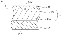
- FIG. 2 shows an example of a laminate 20 using an insulating sheet having two resin composition layers.
- the resin composition layer 24A is formed from the metal base plate 26 side.
- An insulating sheet comprising a resin composition layer 24 having a (second resin composition layer) and a resin composition layer 24B (first resin composition layer) in this order is provided.
- the relative dielectric constant can be changed between the upper and lower layers.
- the thickness of a 1st resin composition layer is smaller than the thickness of a 2nd resin composition layer, and the thickness of a 1st layer is 2/5 with respect to the thickness of a 2nd layer. Or less, more preferably 1/3 or less.
- the electric field concentration can be further relaxed and the insulation can be further improved.
- one surface side is the upper surface 24X side (metal plate 22 side) of the resin composition layer 24B, and the other surface side is the lower surface 24Y side (metal base plate 26 side) of the resin composition layer 24A. It becomes.
- FIG. 3 is an example of the laminated body 30 using the insulating sheet whose resin composition layer is three layers. That is, the resin composition layer 34A (third resin composition layer), the resin composition layer 34B (second resin composition layer) from the metal base plate 36 side between the metal plate 32 and the metal base plate 36, And the insulating sheet which consists of the resin composition layer 34 which has the resin composition layer 34C (1st resin composition layer) in this order is provided.
- the resin composition layer By making the resin composition layer into at least three layers, the relative dielectric constant gradually decreases from one surface side to the other surface side by gradually reducing the relative dielectric constant in the upper layer, intermediate layer, and lower layer. Can be lowered. As a result, higher insulation can be exhibited.
- one surface side is the upper surface 34X side (metal plate 32 side) of the resin composition layer 34C, and the other surface side is the lower surface 34Y side (metal base plate 36 side) of the resin composition layer 34A. It becomes.
- the resin composition layer 24A may include plate-like inorganic particles, and the resin composition layer 24B may include inorganic particles A and inorganic particles B.
- the resin composition layer 24A may include inorganic particles A and inorganic particles B, and the resin composition layer 24B may include plate-like inorganic particles.
- the resin composition layer 24A contains a plate-like inorganic particle, and more preferably, the resin composition layer 24A contains a plate-like inorganic particle, and the resin composition layer 24B contains the inorganic particle A and inorganic particles.
- a configuration in which the particles B are contained is mentioned.
- the plate-like inorganic particles and the inorganic particles B are boron nitride aggregated particles
- the inorganic particles A are alumina particles
- the 20% compressive strength of the plate-like inorganic particles is lower than the 20% compressive strength of the inorganic particles B
- the thermal conductivity the adhesion between the metal plate 22 and the resin composition layer 24B can be improved while making the insulation better.
- the content of the plate-like inorganic particles in the resin composition layer 24A is as follows. It is preferably 3% by volume or more, more preferably 5% by volume or more, more preferably 90% by volume or less, and even more preferably 85% by volume.
- the epoxy resin is preferably 5% by volume or more, more preferably 10% by volume or more, and preferably 60% by volume or less, more preferably 50% by volume or less. .
- the content of the inorganic particles A in the resin composition layer 24B is preferably 1% by volume or more, more preferably 3% by volume or more, and preferably 60% by volume or less. More preferably, it is 50 volume% or less.
- the content of the inorganic particles B is preferably 1% by volume or more, more preferably 3% by volume or more, more preferably 90% by volume or less, and more preferably 85% by volume or less. preferable.
- the epoxy resin is preferably 5% by volume or more, more preferably 10% by volume or more, and preferably 60% by volume or less, more preferably 50% by volume or less. .
- the total content in each layer of the inorganic filler including the plate-like inorganic particles, the inorganic particles A, and the inorganic particles B, and the total content in each layer of the epoxy resin Is the same as in the case of a single resin composition layer.
- the thickness of the resin composition layer 24A on the metal base plate side is preferably 20 ⁇ m or more, more preferably 50 ⁇ m or more, and 170 ⁇ m or less. Preferably, it is 150 ⁇ m or less.
- the thickness of the resin composition layer 24B on the metal plate side is preferably 10 ⁇ m or more, more preferably 20 ⁇ m or more, more preferably 150 ⁇ m or less, and even more preferably 130 ⁇ m or less. At this time, the thickness of the resin composition layer 24B is preferably smaller than the thickness of the resin composition layer 24A on the metal base plate side.
- the total thickness of each layer is the same as in the case where the resin composition layer is one layer, and is preferably 30 ⁇ m or more, preferably 50 ⁇ m or more. More preferably, it is 320 ⁇ m or less, and more preferably 280 ⁇ m or less.
- a resin composition (for example, containing an inorganic filler having a low relative dielectric constant) to be the second resin composition layer is applied on a metal base plate, After semi-curing as necessary, a resin composition (for example, containing an inorganic filler having a high relative dielectric constant) to be the first resin composition layer is further applied thereon, and semi-cured as necessary. Harden. Then, it can manufacture by bonding a metal plate and performing a press process. In addition, both sides of the laminated sheet of the sheet made of the resin composition to be the first resin composition layer and the sheet made of the resin composition to be the second resin composition layer are sandwiched between the metal base plate and the metal plate, respectively. It can also be manufactured by pressing.
- the plate-like inorganic particles, the inorganic particles A, and the inorganic particles B blended in the resin composition layers 34A, 34B, and 34C have a desired dielectric constant. It can be appropriately selected from the viewpoint.
- the resin composition layer 34A third resin composition layer
- the resin composition layer 34B second resin
- the composition layer includes plate-like inorganic particles
- the resin composition layer 34C first resin composition layer
- the resin composition layer 34A (third resin composition layer) includes plate-like inorganic particles
- the resin composition layer 34B (second resin composition layer) is a plate.
- the resin composition layer 34 ⁇ / b> C (first resin composition layer) includes the inorganic particles A and the inorganic particles B, and includes the inorganic particles A, the inorganic particles A, and the inorganic particles B.
- the first example is preferable.
- the plate-like inorganic particles and the inorganic particles B are boron nitride aggregated particles
- the inorganic particles A are alumina particles
- the 20% compressive strength of the plate-like inorganic particles is inorganic.
- the adhesion between the metal plate 32 and the resin composition layer 34B can be improved while the thermal conductivity and insulation are improved.
- the content of the plate-like inorganic particles in the resin composition layer 34A is preferably 10% by volume or more, and 15% by volume or more. More preferably, it is preferably 80% by volume or less, and more preferably 70% by volume.
- the content of the inorganic particles A is preferably 10% by volume or more, more preferably 20% by volume or more, more preferably 70% by volume or less, and more preferably 60% by volume or less. preferable.
- the content of the inorganic particles B is preferably 10% by volume or more, more preferably 20% by volume or more, more preferably 80% by volume or less, and more preferably 70% by volume or less. preferable.
- the epoxy resin is preferably 10% by volume or more, more preferably 20% by volume or more, and preferably 70% by volume or less, more preferably 50% by volume or less.
- the content of the plate-like inorganic particles in the resin composition layer 34B (second resin composition layer) is preferably 20% by volume or more, more preferably 30% by volume or more, and 85% by volume. % Or less, and more preferably 75% by volume or less.
- the epoxy resin is preferably 10% by volume or more, more preferably 20% by volume or more, and preferably 50% by volume or less, more preferably 70% by volume or less. .
- the content of the inorganic particles A in the resin composition layer 34C is preferably 5% by volume or more, more preferably 10% by volume or more, and 80% by volume. Or less, more preferably 70% by volume or less.
- the content of the inorganic particles B is preferably 10% by volume or more, more preferably 15% by volume or more, more preferably 70% by volume or less, and more preferably 50% by volume or less.
- the epoxy resin is preferably 10% by volume or more, more preferably 20% by volume or more, and preferably 70% by volume or less, more preferably 50% by volume or less. .
- the content of the plate-like inorganic particles in the resin composition layer 34A is preferably 10% by volume or more, and 20% by volume or more. More preferably, it is preferably 85% by volume or less, and more preferably 75% by volume.
- the epoxy resin is preferably 10% by volume or more, more preferably 20% by volume or more, and preferably 70% by volume or less, more preferably 50% by volume or less.
- the content of the plate-like inorganic particles in the resin composition layer 34B (second resin composition layer) is preferably 10% by volume or more, more preferably 20% by volume or more, and 80% by volume. % Or less is preferable, and 70% by volume or less is more preferable.
- the content of the inorganic particles A is preferably 10% by volume or more, more preferably 20% by volume or more, more preferably 80% by volume or less, and more preferably 70% by volume or less. preferable.
- the content of the inorganic particles B is preferably 5% by volume or more, more preferably 15% by volume or more, more preferably 80% by volume or less, and more preferably 70% by volume or less. preferable.
- the epoxy resin is preferably 10% by volume or more, more preferably 20% by volume or more, and preferably 50% by volume or less, more preferably 70% by volume or less. .
- the content of the inorganic particles A in the resin composition layer 34C is preferably 5% by volume or more, more preferably 10% by volume or more, and 80% by volume. The following is preferable, and 60% by volume is more preferable.
- the content of the inorganic particles B is preferably 10% by volume or more, more preferably 20% by volume or more, more preferably 80% by volume or less, and more preferably 70% by volume or less.
- the epoxy resin is preferably 10% by volume or more, more preferably 20% by volume or more, and preferably 70% by volume or less, more preferably 50% by volume or less. .
- the total content in each layer of the inorganic filler including the plate-like inorganic particles, the inorganic particles A, and the inorganic particles B, and the total content in each layer of the epoxy resin Is the same as in the case of a single resin composition layer.
- the thickness of the resin composition layer 34C is preferably 10 ⁇ m or more, more preferably 20 ⁇ m or more, preferably 100 ⁇ m or less, and 60 ⁇ m or less. It is more preferable that The thickness of the resin composition layer 34B is preferably 20 ⁇ m or more, more preferably 30 ⁇ m or more, preferably 170 ⁇ m or less, and more preferably 160 ⁇ m or less.
- the thickness of the resin composition layer 34A is preferably 10 ⁇ m or more, more preferably 20 ⁇ m or more, preferably 100 ⁇ m or less, and more preferably 60 ⁇ m or less.
- the thickness of the resin composition 34A (third resin composition layer) is preferably smaller than the thickness of the resin composition layer 34B (second resin composition layer), and the third The resin composition layer is preferably 2/5 or less, more preferably 1/3 or less of the thickness of the second resin composition layer.
- the total thickness of each layer is the same as in the case where the resin composition layer is one layer, preferably 30 ⁇ m or more, and preferably 50 ⁇ m or more. More preferably, it is 320 ⁇ m or less, and more preferably 280 ⁇ m or less.
- a resin composition (for example, a low relative dielectric constant) to be a third resin composition layer is applied on a metal base plate, and half as necessary.
- a resin composition (for example, having a medium relative dielectric constant) to be the second resin composition layer is further applied thereon, and semi-cured as necessary.
- a resin composition (for example, having a high relative dielectric constant) to be the first resin composition layer is applied on the second resin composition layer, and semi-cured as necessary. And it can manufacture by bonding a metal plate and performing a press process.
- seat consisting of the resin composition used as the 1st resin composition layer
- seat consisting of the resin composition used as the 2nd resin composition layer
- the insulating sheet of the present invention as described above is sandwiched between the metal plate and the metal base plate to form a laminated plate, and the metal plate can be used as an insulating circuit substrate by forming a circuit by a technique such as etching. .
- the laminated body of this invention contains the insulating sheet and metal plate of this invention in order on a metal base board.
- a circuit pattern is formed on the metal plate.
- a known method can be applied as a method of laminating these.
- the laminate of the present invention include, but are not limited to, the laminates shown in FIGS.
- substrate of this invention contains the insulating sheet and metal plate of this invention in order on a metal base plate, and a metal plate has a circuit pattern. That is, the substrate of the present invention can be said to be a substrate in which a circuit pattern is formed on the metal plate of the laminate of the present invention. For the formation of the circuit pattern, a technique such as etching can be applied.
- the thermal conductivity is preferably 10 W / (m ⁇ K) or more.
- materials used for these include aluminum, copper, gold, silver, and graphite sheets. From the viewpoint of more effectively increasing the thermal conductivity, aluminum, copper, or gold is preferable, and aluminum or copper is more preferable.
- the thickness of the metal base plate is preferably 0.1 to 5 mm, and the thickness of the metal plate is preferably 10 to 2000 ⁇ m, more preferably 10 to 900 ⁇ m.
- the metal plate includes a plate such as a copper plate and a foil such as a copper foil.
- Example 1 Preparation of resin composition (1)
- Resin composition A Aggregated boron nitride particles 38.3% by volume as inorganic particles B, alumina particles 24.9% by volume, epoxy compound 33.2% by volume, curing agent 2.0% by volume, and dispersant 1.6% by volume. These were mixed and the resin composition A was obtained. Details of the above materials are as follows.
- Aggregated boron nitride particles as inorganic particles B UHP-G1H, Showa Denko KK, 20% compressive strength 4.2 N / mm 2 Alumina particles: AS50, Showa Denko, aspect ratio 2 Epoxy compound: YD127, manufactured by Nippon Steel & Sumikin Co., Ltd. Curing agent: 2P4MZ, manufactured by Shikoku Kasei Co., Ltd. Dispersant: KBM403, manufactured by Shin-Etsu Silicone Co., Ltd.
- Resin composition B These are mixed so that the aggregated boron nitride particles as plate-like inorganic particles are 67.5% by volume, the epoxy compound is 29.3% by volume, the curing agent is 2.0% by volume, and the dispersing agent is 1.2% by volume. B was obtained. Details of the above materials are as follows.
- Aggregated boron nitride particles as plate-like inorganic particles HP-40, manufactured by Mizushima Alloy Iron Co., Ltd., 20% compressive strength 1.7 N / mm 2
- Epoxy compound YD127, manufactured by Nippon Steel & Sumikin Co., Ltd.
- the resin composition A was apply
- the resin composition B was apply
- Table 1 shows the thickness ratio of the resin composition layers of these sheets. These were dried in a 50 ° C. oven for 10 minutes and temporarily cured. Next, the pre-cured sheet is laminated so that the release PET sheet is on the outside, and then the release PET sheet is peeled off. And heated at 110 ° C. for 30 minutes for temporary curing to obtain a pre-cured sheet.
- a layer containing the resin composition A (first resin composition layer) is formed on the copper foil side, and a layer containing the resin composition B (second resin composition layer) is formed on the aluminum plate side.
- the obtained pre-cured sheet is vacuum-pressed for 60 minutes under the conditions of a temperature of 195 ° C. and a pressure of 8 MPa, whereby the first resin of the insulating sheet comprising the first resin composition layer and the second resin composition layer A copper foil was laminated on the composition layer, and a laminate in which an aluminum plate was laminated on the second resin composition layer was obtained.
- the thickness (thickness of an insulating sheet) of the resin composition layer which consists of a 1st resin composition layer and a 2nd resin composition layer was 150 micrometers.
- Example 2 and 3 Except for changing the thickness ratio between the first resin composition layer and the second resin composition layer (second resin composition layer / first resin composition layer) as shown in Table 1 below. In the same manner as in Example 1, an insulating sheet was obtained.
- Aggregated boron nitride particles as plate-like inorganic particles HP-40, manufactured by Mizushima Alloy Iron Co., Ltd., 20% compressive strength 1.7 N / mm 2
- Aggregated boron nitride particles as inorganic particles B UHP-G1H, Showa Denko KK, 20% compressive strength 4.2 N / mm 2
- Dispersant KBM403, manufactured by Shin-Etsu Silicone Co., Ltd.
- the resin composition A was apply
- the resin composition B was apply
- the resin composition C was applied onto a release PET sheet (thickness 40 ⁇ m). Table 1 shows the thickness ratio of the resin composition layers of these sheets. These were dried in a 50 ° C. oven for 10 minutes and temporarily cured. Next, among the pre-cured sheets, the release PET sheet coated with the resin composition A, the release PET sheet coated with the resin composition B, and the respective release PET sheets are laminated so as to be outside. The release PET sheet coated with the resin composition B was peeled off.
- coated the resin composition C to the surface of the resin composition B exposed on the surface was laminated
- the both sides were sandwiched between a copper foil (thickness 40 ⁇ m) and an aluminum plate (thickness 1.0 mm), respectively, heated at 110 ° C. for 30 minutes and temporarily cured, A sheet before curing was obtained.
- a layer containing the resin composition A (first resin composition layer) is formed on the copper foil side, and a layer containing the resin composition C (third resin composition layer) is formed on the aluminum plate side.
- the obtained pre-cured sheet was vacuum-pressed for 60 minutes at a temperature of 195 ° C. and a pressure of 8 MPa.
- the copper foil was laminated
- the thickness of the resin composition layer (thickness of the insulating sheet) composed of the first resin composition layer, the second resin composition layer, and the third resin composition layer was 200 ⁇ m.
- Example 5 Production of insulating sheet A layer containing the resin composition A (first resin composition layer) is formed on the copper foil side, and a layer containing the resin composition B (third resin composition layer) on the aluminum plate side ) And a layer containing the resin composition C (second resin composition layer) is formed between them, and the thickness ratio shown in Table 1 is the same as in Example 4. Similarly, a sheet before curing was obtained. From the first resin composition layer, the second resin composition layer, and the third resin composition layer, the obtained pre-cured sheet was vacuum-pressed for 60 minutes at a temperature of 195 ° C. and a pressure of 8 MPa.
- the copper foil was laminated
- the thickness of the resin composition layer (thickness of the insulating sheet) composed of the first resin composition layer, the second resin composition layer, and the third resin composition layer was 200 ⁇ m.
- Example 1 An insulating sheet was obtained in the same manner as in Example 1 except that the resin composition layer was only the second resin composition layer.
- the total thickness of the resin composition layer (the thickness of the insulating sheet) is the same as in Example 1.
- Example 2 An insulating sheet was obtained in the same manner as in Example 1 except that only the first resin composition layer was used as the resin composition layer.
- the total thickness of the resin composition layer (the thickness of the insulating sheet) is the same as in Example 1.
- the first resin of the insulating sheet comprising the first resin composition layer and the second resin composition layer A copper foil was laminated on the composition layer, and a laminate in which an aluminum plate was laminated on the second resin composition layer was obtained.
- the first resin composition layer and the second resin composition layer have the same composition.
- the entire thickness of the resin composition layer (the thickness of the insulating sheet) is the same as that of Example 1.
- Example 4 A layer containing the resin composition B (first resin composition layer) is formed on the copper foil side, and a layer containing the resin composition A (second resin composition layer) is formed on the aluminum plate side. In the same manner as in Example 1, an insulating sheet was obtained. The total thickness of the resin composition layer (the thickness of the insulating sheet) is the same as in Example 1.
- the copper foil was laminated
- the thickness of the resin composition layer (thickness of the insulating sheet) composed of the first resin composition layer, the second resin composition layer, and the third resin composition layer was 200 ⁇ m.
- the release PET sheets on both sides of the sheet temporarily cured in “Preparation of Insulating Sheet” in each example are peeled off, and both sides are sandwiched between a copper foil (thickness 40 ⁇ m) and an aluminum plate (thickness 1.0 mm), respectively.
- a pre-cured sheet was obtained by heating at 110 ° C. for 30 minutes for temporary curing.
- the obtained uncured sheet was vacuum-pressed for 60 minutes under the conditions of a temperature of 195 ° C. and a pressure of 8 MPa to obtain a sample sheet.
- the obtained sample sheet was cut into 40 mm ⁇ 40 mm, and a ⁇ 20 mm pattern was processed by etching. The etching depth was 10% in the thickness direction.
- the relative permittivity was measured at 33 points and 1 cycle by dividing the frequency range from 100 mHz to 10 MHz on a log scale at room temperature (25 ° C) in air with an LCR (impedance) analyzer PSM3750 manufactured by Iwasaki Tsushin Co., Ltd.
- the relative dielectric constant at a frequency of 1 MHz was obtained by reading the obtained waveform.
- thermal conductivity was measured by a laser flash method using a measurement sample sprayed with carbon black on both sides. The results are shown in Tables 1 to 3 below. [Thermal conductivity criteria] A: 10 W or more B: 8 W or more to less than 10 W C: less than 8 W
- Each insulating sheet of the example and the comparative example is cut into 90 mm ⁇ 50 mm, and a pattern of ⁇ 20 mm is processed by etching on the insulating sheet, and then between the test samples using a withstand voltage tester (“MODEL7473” manufactured by EXTECH Electronics). AC voltage was applied so that the voltage increased at a rate of 0.5 kV / min.
- the breakdown voltage of the test sample was defined as a breakdown voltage (BDV), and the results are shown in Tables 1 to 3 below. Insulation was judged according to the following criteria.
- the thickness of the resin composition layer (insulating layer) to be measured was 150 ⁇ m.
- Dielectric breakdown voltage is 10 kV or more
- the laminated body obtained by the Example and the comparative example was cut out to the magnitude
- the obtained test sample was peeled off leaving only the copper foil having a center width of 10 mm, and the peel strength of the 35 ⁇ m copper foil was measured in accordance with JIS C 6481 with respect to the copper foil having a center width of 10 mm.
- As the peel strength measuring apparatus “Tensilon universal testing machine” manufactured by Orientec Co., Ltd. was used.
- the peel strength was determined according to the following criteria. The results are shown in Tables 1 to 3 below.
- Peel strength criteria A: Peel strength is 6 N / cm or more C: Peel strength is less than 6 N / cm
Landscapes
- Chemical & Material Sciences (AREA)
- Health & Medical Sciences (AREA)
- Chemical Kinetics & Catalysis (AREA)
- Medicinal Chemistry (AREA)
- Polymers & Plastics (AREA)
- Organic Chemistry (AREA)
- Engineering & Computer Science (AREA)
- Microelectronics & Electronic Packaging (AREA)
- Physics & Mathematics (AREA)
- Spectroscopy & Molecular Physics (AREA)
- Laminated Bodies (AREA)
- Compositions Of Macromolecular Compounds (AREA)
- Organic Insulating Materials (AREA)
- Insulating Bodies (AREA)
- Insulated Metal Substrates For Printed Circuits (AREA)
- Inorganic Insulating Materials (AREA)
Abstract
Priority Applications (5)
| Application Number | Priority Date | Filing Date | Title |
|---|---|---|---|
| CN201980017937.0A CN111837203A (zh) | 2018-04-17 | 2019-04-17 | 绝缘片、叠层体及基板 |
| US16/977,569 US11548264B2 (en) | 2018-04-17 | 2019-04-17 | Insulation sheet, laminate, and substrate |
| JP2020514410A JP6844066B2 (ja) | 2018-04-17 | 2019-04-17 | 絶縁シート、積層体、及び基板 |
| EP19788343.2A EP3748654A4 (fr) | 2018-04-17 | 2019-04-17 | Feuille d'isolation, stratifié et substrat |
| KR1020207025496A KR102438092B1 (ko) | 2018-04-17 | 2019-04-17 | 절연 시트, 적층체, 및 기판 |
Applications Claiming Priority (2)
| Application Number | Priority Date | Filing Date | Title |
|---|---|---|---|
| JP2018-079028 | 2018-04-17 | ||
| JP2018079028 | 2018-04-17 |
Publications (1)
| Publication Number | Publication Date |
|---|---|
| WO2019203266A1 true WO2019203266A1 (fr) | 2019-10-24 |
Family
ID=68239657
Family Applications (1)
| Application Number | Title | Priority Date | Filing Date |
|---|---|---|---|
| PCT/JP2019/016454 WO2019203266A1 (fr) | 2018-04-17 | 2019-04-17 | Feuille d'isolation, stratifié et substrat |
Country Status (7)
| Country | Link |
|---|---|
| US (1) | US11548264B2 (fr) |
| EP (1) | EP3748654A4 (fr) |
| JP (2) | JP6844066B2 (fr) |
| KR (1) | KR102438092B1 (fr) |
| CN (1) | CN111837203A (fr) |
| TW (1) | TW201943565A (fr) |
| WO (1) | WO2019203266A1 (fr) |
Cited By (3)
| Publication number | Priority date | Publication date | Assignee | Title |
|---|---|---|---|---|
| JP2021104672A (ja) * | 2018-04-17 | 2021-07-26 | 積水化学工業株式会社 | 絶縁シート、積層体、及び基板 |
| WO2022045663A1 (fr) * | 2020-08-25 | 2022-03-03 | 엘지이노텍 주식회사 | Composition de résine pour boîtier de semi-conducteur et résine fixée à une feuille de cuivre la comprenant |
| WO2022255130A1 (fr) * | 2021-05-31 | 2022-12-08 | 富士フイルム株式会社 | Feuille thermoconductrice, et dispositif équipé de celle-ci |
Families Citing this family (2)
| Publication number | Priority date | Publication date | Assignee | Title |
|---|---|---|---|---|
| WO2020095988A1 (fr) * | 2018-11-08 | 2020-05-14 | 株式会社クラレ | Film polymère thermoplastique à cristaux liquides et carte de circuit imprimé l'utilisant |
| JPWO2022220261A1 (fr) | 2021-04-14 | 2022-10-20 |
Citations (6)
| Publication number | Priority date | Publication date | Assignee | Title |
|---|---|---|---|---|
| JPH0424996A (ja) * | 1990-05-15 | 1992-01-28 | Matsushita Electric Works Ltd | 多層プリント基板の製造方法 |
| JPH07232403A (ja) * | 1994-02-23 | 1995-09-05 | Matsushita Electric Works Ltd | 金属張り積層板の製造方法 |
| JP2008201124A (ja) * | 2007-01-24 | 2008-09-04 | Hitachi Chem Co Ltd | 電気絶縁用積層材料及びこの積層材料を用いたプリント配線板 |
| JP2008270678A (ja) * | 2007-04-25 | 2008-11-06 | Mitsubishi Electric Corp | 絶縁シートおよび半導体装置 |
| JP2012015557A (ja) | 2011-10-19 | 2012-01-19 | Mitsubishi Electric Corp | 絶縁シートおよび半導体装置 |
| WO2012172776A1 (fr) * | 2011-06-17 | 2012-12-20 | パナソニック株式会社 | Plaque stratifiée plaquée de métal et carte de circuit imprimé |
Family Cites Families (18)
| Publication number | Priority date | Publication date | Assignee | Title |
|---|---|---|---|---|
| JPH06152088A (ja) * | 1992-11-05 | 1994-05-31 | Furukawa Electric Co Ltd:The | 金属ベースプリント配線基板 |
| JP2756075B2 (ja) * | 1993-08-06 | 1998-05-25 | 三菱電機株式会社 | 金属ベース基板およびそれを用いた電子機器 |
| JP2010186789A (ja) * | 2009-02-10 | 2010-08-26 | Hitachi Ltd | 絶縁回路基板、インバータ装置、及びパワー半導体装置 |
| JP2011070930A (ja) * | 2009-09-25 | 2011-04-07 | Sekisui Chem Co Ltd | 多層絶縁シート及び積層構造体 |
| US20120325473A1 (en) * | 2010-03-15 | 2012-12-27 | Sun Drilling Products Corporation | Catalytic polymer bead compositions; processiing for their production; and their use in generating and extracting natural gas, light crude oil, or sequences or mixtures thereof |
| US20130149514A1 (en) * | 2010-07-30 | 2013-06-13 | Kyocera Corporation | Insulating sheet, method of manufacturing the same, and method of manufacturing structure using the insulating sheet |
| KR101784196B1 (ko) * | 2010-08-26 | 2017-10-11 | 덴카 주식회사 | 수지 조성물 및 상기 수지 조성물로 이루어지는 성형체와 기판재 및 상기 기판재를 포함하여 이루어지는 회로기판 |
| JP2012067221A (ja) * | 2010-09-24 | 2012-04-05 | Sekisui Chem Co Ltd | 絶縁シート及び積層構造体 |
| JP5831122B2 (ja) * | 2010-10-18 | 2015-12-09 | 三菱化学株式会社 | 三次元集積回路用の層間充填材組成物、塗布液及び三次元集積回路の製造方法 |
| JP2012253167A (ja) * | 2011-06-02 | 2012-12-20 | Denki Kagaku Kogyo Kk | 熱伝導性絶縁シート、金属ベース基板及び回路基板 |
| JP2013098217A (ja) * | 2011-10-28 | 2013-05-20 | Sekisui Chem Co Ltd | パワー半導体モジュール用部品の製造方法 |
| CN103748673B (zh) * | 2011-10-28 | 2016-12-14 | 积水化学工业株式会社 | 叠层体及功率半导体模块用部件的制造方法 |
| US9382445B2 (en) | 2012-09-07 | 2016-07-05 | Sekisui Chemical Co., Ltd. | Insulating resin material and multilayer substrate |
| EP3069868A1 (fr) * | 2015-03-17 | 2016-09-21 | ABB Technology Ltd | Matériau d'isolation électrique inorganique |
| KR102512228B1 (ko) * | 2015-10-01 | 2023-03-21 | 삼성전기주식회사 | 절연재 및 이를 포함하는 인쇄회로기판 |
| KR102460757B1 (ko) * | 2015-12-23 | 2022-10-31 | 삼성전기주식회사 | 절연수지 시트 및 이를 구비한 인쇄회로기판 |
| EP3722091B1 (fr) * | 2017-12-08 | 2023-11-15 | Sekisui Chemical Co., Ltd. | Stratifié et dispositif électronique |
| TW201943565A (zh) * | 2018-04-17 | 2019-11-16 | 日商積水化學工業股份有限公司 | 絕緣片、積層體、及基板 |
-
2019
- 2019-04-17 TW TW108113403A patent/TW201943565A/zh unknown
- 2019-04-17 EP EP19788343.2A patent/EP3748654A4/fr active Pending
- 2019-04-17 WO PCT/JP2019/016454 patent/WO2019203266A1/fr active Application Filing
- 2019-04-17 JP JP2020514410A patent/JP6844066B2/ja active Active
- 2019-04-17 KR KR1020207025496A patent/KR102438092B1/ko active IP Right Grant
- 2019-04-17 CN CN201980017937.0A patent/CN111837203A/zh active Pending
- 2019-04-17 US US16/977,569 patent/US11548264B2/en active Active
-
2021
- 2021-02-24 JP JP2021027830A patent/JP2021104672A/ja active Pending
Patent Citations (6)
| Publication number | Priority date | Publication date | Assignee | Title |
|---|---|---|---|---|
| JPH0424996A (ja) * | 1990-05-15 | 1992-01-28 | Matsushita Electric Works Ltd | 多層プリント基板の製造方法 |
| JPH07232403A (ja) * | 1994-02-23 | 1995-09-05 | Matsushita Electric Works Ltd | 金属張り積層板の製造方法 |
| JP2008201124A (ja) * | 2007-01-24 | 2008-09-04 | Hitachi Chem Co Ltd | 電気絶縁用積層材料及びこの積層材料を用いたプリント配線板 |
| JP2008270678A (ja) * | 2007-04-25 | 2008-11-06 | Mitsubishi Electric Corp | 絶縁シートおよび半導体装置 |
| WO2012172776A1 (fr) * | 2011-06-17 | 2012-12-20 | パナソニック株式会社 | Plaque stratifiée plaquée de métal et carte de circuit imprimé |
| JP2012015557A (ja) | 2011-10-19 | 2012-01-19 | Mitsubishi Electric Corp | 絶縁シートおよび半導体装置 |
Non-Patent Citations (1)
| Title |
|---|
| See also references of EP3748654A4 |
Cited By (3)
| Publication number | Priority date | Publication date | Assignee | Title |
|---|---|---|---|---|
| JP2021104672A (ja) * | 2018-04-17 | 2021-07-26 | 積水化学工業株式会社 | 絶縁シート、積層体、及び基板 |
| WO2022045663A1 (fr) * | 2020-08-25 | 2022-03-03 | 엘지이노텍 주식회사 | Composition de résine pour boîtier de semi-conducteur et résine fixée à une feuille de cuivre la comprenant |
| WO2022255130A1 (fr) * | 2021-05-31 | 2022-12-08 | 富士フイルム株式会社 | Feuille thermoconductrice, et dispositif équipé de celle-ci |
Also Published As
| Publication number | Publication date |
|---|---|
| JP2021104672A (ja) | 2021-07-26 |
| KR20200106983A (ko) | 2020-09-15 |
| EP3748654A4 (fr) | 2021-04-07 |
| US20210008839A1 (en) | 2021-01-14 |
| EP3748654A1 (fr) | 2020-12-09 |
| JP6844066B2 (ja) | 2021-03-17 |
| CN111837203A (zh) | 2020-10-27 |
| TW201943565A (zh) | 2019-11-16 |
| KR102438092B1 (ko) | 2022-08-30 |
| JPWO2019203266A1 (ja) | 2021-02-12 |
| US11548264B2 (en) | 2023-01-10 |
Similar Documents
| Publication | Publication Date | Title |
|---|---|---|
| WO2019203266A1 (fr) | Feuille d'isolation, stratifié et substrat | |
| US11034623B2 (en) | Thermal conductive member and heat dissipation structure including the same | |
| JP6023474B2 (ja) | 熱伝導性絶縁シート、金属ベース基板及び回路基板、及びその製造方法 | |
| EP3305856A1 (fr) | Composition de résine, feuille de résine, préimprégné, matériau isolant, article durci à base d'une feuille de résine, et élément de dissipation de chaleur | |
| JP6945241B2 (ja) | フィルム用樹脂組成物、フィルム、基材付フィルム、金属/樹脂積層体、樹脂硬化物、半導体装置、および、フィルム製造方法 | |
| KR102524227B1 (ko) | 수지 재료, 수지 재료의 제조 방법 및 적층체 | |
| JP2007153969A (ja) | 高熱伝導性樹脂組成物および配線用基板 | |
| WO2014021427A1 (fr) | Carte à circuit imprimé à base métallique | |
| EP2641736A1 (fr) | Feuille en résine multicouche et stratifié de feuilles de résine | |
| KR20190090843A (ko) | 방열 회로 기판 | |
| TWI801547B (zh) | 散熱片、散熱構件及半導體元件 | |
| JP2019150997A (ja) | 積層体 | |
| JP2020102556A (ja) | 積層体、電子部品、及びインバータ | |
| WO2019168155A1 (fr) | Corps stratifié | |
| WO2021149690A1 (fr) | Feuille thermoconductrice, stratifié et dispositif à semi-conducteur | |
| JP7295635B2 (ja) | 積層体、電子部品およびインバータ | |
| US20100028689A1 (en) | B-stage thermal conductive dielectric coated metal-plate and method of making same | |
| JP7069967B2 (ja) | 放熱基板 | |
| JP2022151865A (ja) | 積層構造体およびその製造方法 | |
| JP2023033211A (ja) | 絶縁樹脂シート、積層体、及び半導体装置 | |
| TW202248317A (zh) | 樹脂片、積層體、及半導體裝置 | |
| JP2023048546A (ja) | 熱伝導性接着シート |
Legal Events
| Date | Code | Title | Description |
|---|---|---|---|
| 121 | Ep: the epo has been informed by wipo that ep was designated in this application |
Ref document number: 19788343 Country of ref document: EP Kind code of ref document: A1 |
|
| DPE1 | Request for preliminary examination filed after expiration of 19th month from priority date (pct application filed from 20040101) | ||
| WWE | Wipo information: entry into national phase |
Ref document number: 2020514410 Country of ref document: JP |
|
| ENP | Entry into the national phase |
Ref document number: 20207025496 Country of ref document: KR Kind code of ref document: A |
|
| ENP | Entry into the national phase |
Ref document number: 2019788343 Country of ref document: EP Effective date: 20200901 |
|
| NENP | Non-entry into the national phase |
Ref country code: DE |