WO2019193643A1 - 半導体装置の製造方法 - Google Patents
半導体装置の製造方法 Download PDFInfo
- Publication number
- WO2019193643A1 WO2019193643A1 PCT/JP2018/014216 JP2018014216W WO2019193643A1 WO 2019193643 A1 WO2019193643 A1 WO 2019193643A1 JP 2018014216 W JP2018014216 W JP 2018014216W WO 2019193643 A1 WO2019193643 A1 WO 2019193643A1
- Authority
- WO
- WIPO (PCT)
- Prior art keywords
- solder
- end surface
- barrier layer
- view
- laser chip
- Prior art date
- Legal status (The legal status is an assumption and is not a legal conclusion. Google has not performed a legal analysis and makes no representation as to the accuracy of the status listed.)
- Ceased
Links
Images
















Classifications
-
- H—ELECTRICITY
- H01—ELECTRIC ELEMENTS
- H01S—DEVICES USING THE PROCESS OF LIGHT AMPLIFICATION BY STIMULATED EMISSION OF RADIATION [LASER] TO AMPLIFY OR GENERATE LIGHT; DEVICES USING STIMULATED EMISSION OF ELECTROMAGNETIC RADIATION IN WAVE RANGES OTHER THAN OPTICAL
- H01S5/00—Semiconductor lasers
- H01S5/02—Structural details or components not essential to laser action
- H01S5/022—Mountings; Housings
- H01S5/0235—Method for mounting laser chips
- H01S5/02355—Fixing laser chips on mounts
- H01S5/0237—Fixing laser chips on mounts by soldering
-
- H—ELECTRICITY
- H01—ELECTRIC ELEMENTS
- H01S—DEVICES USING THE PROCESS OF LIGHT AMPLIFICATION BY STIMULATED EMISSION OF RADIATION [LASER] TO AMPLIFY OR GENERATE LIGHT; DEVICES USING STIMULATED EMISSION OF ELECTROMAGNETIC RADIATION IN WAVE RANGES OTHER THAN OPTICAL
- H01S5/00—Semiconductor lasers
- H01S5/02—Structural details or components not essential to laser action
- H01S5/022—Mountings; Housings
- H01S5/0239—Combinations of electrical or optical elements
-
- H—ELECTRICITY
- H01—ELECTRIC ELEMENTS
- H01S—DEVICES USING THE PROCESS OF LIGHT AMPLIFICATION BY STIMULATED EMISSION OF RADIATION [LASER] TO AMPLIFY OR GENERATE LIGHT; DEVICES USING STIMULATED EMISSION OF ELECTROMAGNETIC RADIATION IN WAVE RANGES OTHER THAN OPTICAL
- H01S5/00—Semiconductor lasers
- H01S5/04—Processes or apparatus for excitation, e.g. pumping, e.g. by electron beams
- H01S5/042—Electrical excitation ; Circuits therefor
- H01S5/0425—Electrodes, e.g. characterised by the structure
- H01S5/04256—Electrodes, e.g. characterised by the structure characterised by the configuration
-
- H—ELECTRICITY
- H01—ELECTRIC ELEMENTS
- H01S—DEVICES USING THE PROCESS OF LIGHT AMPLIFICATION BY STIMULATED EMISSION OF RADIATION [LASER] TO AMPLIFY OR GENERATE LIGHT; DEVICES USING STIMULATED EMISSION OF ELECTROMAGNETIC RADIATION IN WAVE RANGES OTHER THAN OPTICAL
- H01S5/00—Semiconductor lasers
- H01S5/02—Structural details or components not essential to laser action
- H01S5/022—Mountings; Housings
- H01S5/02208—Mountings; Housings characterised by the shape of the housings
- H01S5/02212—Can-type, e.g. TO-CAN housings with emission along or parallel to symmetry axis
-
- H—ELECTRICITY
- H01—ELECTRIC ELEMENTS
- H01S—DEVICES USING THE PROCESS OF LIGHT AMPLIFICATION BY STIMULATED EMISSION OF RADIATION [LASER] TO AMPLIFY OR GENERATE LIGHT; DEVICES USING STIMULATED EMISSION OF ELECTROMAGNETIC RADIATION IN WAVE RANGES OTHER THAN OPTICAL
- H01S5/00—Semiconductor lasers
- H01S5/02—Structural details or components not essential to laser action
- H01S5/022—Mountings; Housings
- H01S5/0233—Mounting configuration of laser chips
- H01S5/02345—Wire-bonding
-
- H—ELECTRICITY
- H01—ELECTRIC ELEMENTS
- H01S—DEVICES USING THE PROCESS OF LIGHT AMPLIFICATION BY STIMULATED EMISSION OF RADIATION [LASER] TO AMPLIFY OR GENERATE LIGHT; DEVICES USING STIMULATED EMISSION OF ELECTROMAGNETIC RADIATION IN WAVE RANGES OTHER THAN OPTICAL
- H01S5/00—Semiconductor lasers
- H01S5/02—Structural details or components not essential to laser action
- H01S5/024—Arrangements for thermal management
- H01S5/02469—Passive cooling, e.g. where heat is removed by the housing as a whole or by a heat pipe without any active cooling element like a TEC
-
- H—ELECTRICITY
- H01—ELECTRIC ELEMENTS
- H01S—DEVICES USING THE PROCESS OF LIGHT AMPLIFICATION BY STIMULATED EMISSION OF RADIATION [LASER] TO AMPLIFY OR GENERATE LIGHT; DEVICES USING STIMULATED EMISSION OF ELECTROMAGNETIC RADIATION IN WAVE RANGES OTHER THAN OPTICAL
- H01S5/00—Semiconductor lasers
- H01S5/04—Processes or apparatus for excitation, e.g. pumping, e.g. by electron beams
- H01S5/042—Electrical excitation ; Circuits therefor
- H01S5/0425—Electrodes, e.g. characterised by the structure
- H01S5/04252—Electrodes, e.g. characterised by the structure characterised by the material
-
- H—ELECTRICITY
- H01—ELECTRIC ELEMENTS
- H01S—DEVICES USING THE PROCESS OF LIGHT AMPLIFICATION BY STIMULATED EMISSION OF RADIATION [LASER] TO AMPLIFY OR GENERATE LIGHT; DEVICES USING STIMULATED EMISSION OF ELECTROMAGNETIC RADIATION IN WAVE RANGES OTHER THAN OPTICAL
- H01S5/00—Semiconductor lasers
- H01S5/30—Structure or shape of the active region; Materials used for the active region
- H01S5/3013—AIIIBV compounds
-
- H—ELECTRICITY
- H01—ELECTRIC ELEMENTS
- H01S—DEVICES USING THE PROCESS OF LIGHT AMPLIFICATION BY STIMULATED EMISSION OF RADIATION [LASER] TO AMPLIFY OR GENERATE LIGHT; DEVICES USING STIMULATED EMISSION OF ELECTROMAGNETIC RADIATION IN WAVE RANGES OTHER THAN OPTICAL
- H01S5/00—Semiconductor lasers
- H01S5/30—Structure or shape of the active region; Materials used for the active region
- H01S5/34—Structure or shape of the active region; Materials used for the active region comprising quantum well or superlattice structures, e.g. single quantum well [SQW] lasers, multiple quantum well [MQW] lasers or graded index separate confinement heterostructure [GRINSCH] lasers
- H01S5/343—Structure or shape of the active region; Materials used for the active region comprising quantum well or superlattice structures, e.g. single quantum well [SQW] lasers, multiple quantum well [MQW] lasers or graded index separate confinement heterostructure [GRINSCH] lasers in AIIIBV compounds, e.g. AlGaAs-laser, InP-based laser
- H01S5/34326—Structure or shape of the active region; Materials used for the active region comprising quantum well or superlattice structures, e.g. single quantum well [SQW] lasers, multiple quantum well [MQW] lasers or graded index separate confinement heterostructure [GRINSCH] lasers in AIIIBV compounds, e.g. AlGaAs-laser, InP-based laser with a well layer based on InGa(Al)P, e.g. red laser
Definitions
- the present invention relates to a method for manufacturing a semiconductor device.
- the spread of solder is suppressed by providing a barrier layer between the submount electrode and solder made of, for example, AuSn.
- the material of the barrier layer is Pt.
- the effect of suppressing the wetting and spreading of the solder can be obtained by preventing the reaction between the solder and the Au of the submount electrode by the barrier layer.
- burrs generated during lift-off during the Pt pattern formation serve as a barrier to prevent the solder from spreading.
- Patent Document 1 discloses that when an AuSn solder layer is melted, it does not react with the Au layer due to the presence of a Pt layer as a barrier layer, and maintains the properties as a solder.
- solder burrs are generated at the time of cutting, which may lead to deterioration of characteristics and reliability.
- the present invention has been made in order to solve the above-mentioned problems.
- the sub-surface is designed to improve heat dissipation while suppressing solder wetting and spreading in a direction different from the resonator by 90 °. It is an object of the present invention to provide a method for manufacturing a semiconductor device in which solder easily gets wet to the end of the mount or the vicinity thereof.
- a method of manufacturing a semiconductor device includes a submount substrate having a first end surface and a second end surface facing the first end surface, an electrode layer provided on the submount substrate, and the electrode A barrier layer provided on the layer and extending only to at least one of the first end surface or the second end surface of the end surfaces of the submount substrate in a plan view; and a barrier layer on a side surface of the barrier layer and higher than the barrier layer. And a solder mounted on the barrier layer so as to recede from all end faces of the submount substrate in plan view, and a light emitting stripe region, and a right and left of the light emitting stripe region.
- the extending direction of the melted solder is limited by the burr of the barrier layer, and the solder is extended to the front end face side or the rear end face side of the laser chip, so that the solder is extended to the end of the submount or the vicinity thereof while securing the wire bond area. Can spread wet.
- 1 is a plan view of a semiconductor device according to a first embodiment.
- 1 is a cross-sectional view of a semiconductor device according to a first embodiment.
- 1 is a cross-sectional view of a semiconductor device according to a first embodiment.
- 1 is a plan view of a semiconductor device according to a first embodiment.
- 1 is a cross-sectional view of a semiconductor device according to a first embodiment.
- 1 is a cross-sectional view of a semiconductor device according to a first embodiment.
- It is a top view of the semiconductor device concerning the 1st comparative example. It is sectional drawing of the semiconductor device which concerns on a 1st comparative example.
- FIG. 6 is a plan view of a semiconductor device according to a second embodiment.
- FIG. 6 is a cross-sectional view of a semiconductor device according to a second embodiment.
- FIG. 6 is a cross-sectional view of a semiconductor device according to a second embodiment.
- FIG. 6 is a plan view of a semiconductor device according to a second embodiment.
- FIG. 6 is a cross-sectional view of a semiconductor device according to a second embodiment.
- FIG. 6 is a plan view of a semiconductor device according to a second embodiment.
- FIG. 6 is a cross-sectional view of a semiconductor device according to a second embodiment.
- FIG. 6 is a cross-sectional view of a semiconductor device according to a second embodiment.
- FIG. 6 is a plan view of a semiconductor device according to a third embodiment.
- FIG. 6 is a cross-sectional view of a semiconductor device according to a third embodiment.
- FIG. 6 is a cross-sectional view of a semiconductor device according to a third embodiment.
- FIG. 6 is a plan view of a semiconductor device according to a third embodiment.
- FIG. 6 is a cross-sectional view of a semiconductor device according to a third embodiment.
- FIG. 6 is a cross-sectional view of a semiconductor device according to a third embodiment.
- FIG. 6 is a plan view of a semiconductor device according to a fourth embodiment.
- FIG. 6 is a plan view of a semiconductor device according to a fourth embodiment.
- FIG. 6 is a cross-sectional view of a semiconductor device according to a fourth embodiment.
- FIG. 6 is a cross-sectional view of a semiconductor device according to a fourth embodiment.
- FIG. 6 is a plan view of a semiconductor device according to a fourth embodiment.
- FIG. 6 is a cross-sectional view of a semiconductor device according to a fourth embodiment.
- FIG. 6 is a cross-sectional view of a semiconductor device according to a fourth embodiment.
- FIG. 1 is a perspective view of the semiconductor device according to the first embodiment.
- the laser chip 10 at least a part of which is formed of a semiconductor, is mounted on the submount 19.
- the submount 19 is mounted on the heat sink 14.
- the heat sink 14 is fixed to the stem 16.
- a plurality of terminals 18 penetrating the stem 16 are provided.
- the terminal 18 and the laser chip 10 are electrically connected.
- the upper surface of the laser chip 10 and the terminal 18 are connected by a wire, and the submount 19 and another terminal 18 are connected by another wire.
- FIG. 2 is a cross-sectional view of the laser chip 10 cut perpendicularly to the laser traveling direction.
- the laser chip 10 has a semiconductor substrate 10a.
- a lower cladding layer 10b made of n-type AlInP is formed on the semiconductor substrate 10a.
- the semiconductor substrate 10a and the lower cladding layer 10b are directly bonded.
- a lower light guide layer 10c made of undoped AlInP is formed on the lower cladding layer 10b.
- An active layer 10d made of GaInP is formed on the lower light guide layer 10c.
- An upper light guide layer 10e made of undoped AlGaInP is formed on the active layer 10d.
- An upper clad layer 10f made of p-type AlInP is formed on the upper light guide layer 10e.
- a contact layer 10g made of p-type GaAs is formed on the upper cladding layer 10f.
- the thickness of the semiconductor substrate 10a is 50 to 150 ⁇ m.
- the thickness of the lower cladding layer 10b is 0.5 to 4.0 ⁇ m.
- the carrier concentration of the lower cladding layer 10b is 0.5 to 1.5 ⁇ 10 18 cm ⁇ 3 .
- the thickness of the lower light guide layer 10c and the upper light guide layer 10e is 0.02 to 0.4 ⁇ m.
- the thickness of the active layer 10d is 3.0 to 20 nm.
- the thickness of the upper cladding layer 10f is 0.5 to 4.0 ⁇ m.
- the carrier concentration of the upper cladding layer 10f is 0.5 to 2.0 ⁇ 10 18 cm ⁇ 3 .
- the thickness of the contact layer 10g is 0.05 to 0.5 ⁇ m.
- the carrier concentration of the contact layer 10g is 1.0 to 4.0 ⁇ 10 19 cm ⁇ 3 .
- An insulating film 10h such as a silicon nitride film is formed beside the contact layer 10g.
- the insulating film 10h is etched to have an opening.
- the contact layer other than the opening is removed by etching.
- a p-side electrode 10i is formed on the contact layer 10g and the insulating film 10h.
- the p-side electrode 10i is formed by laminating thin films such as Ti, Pt, and Au.
- the thickness of the p-side electrode 10i is 0.05 to 1.0 ⁇ m.
- the contact layer 10g and the p-side electrode 10i are low-resistance bonded through the opening of the insulating film 10h.
- a gold plating layer 10j is formed on the p-side electrode 10i.
- the thickness of the gold plating layer 10j is 1.0 to 6.0 ⁇ m.
- An n-side electrode 10k is joined to the lower surface of the semiconductor substrate 10a.
- a gold plating layer 101 is formed under the n-side electrode 10k.
- the n-side electrode 10k is formed by laminating thin films such as Ti, Pt, and Au.
- the thickness of the n-side electrode 10k is 0.05 to 1.0 ⁇ m, and the thickness of the gold plating layer 10l is 1.0 to 6.0 ⁇ m.
- the width L1 of the laser chip 10 is 400 ⁇ m.
- the laser chip 10 has a light emission stripe region 10A and left and right adjacent regions 10B of the light emission stripe region 10A.
- the light emitting stripe region 10A is a portion where a contact layer 10g etched so that only the light emitting region remains is formed.
- the width of the light emitting stripe region 10A is 100 ⁇ m.
- the above-mentioned material and a numerical value are an illustration, and it is good also as another material and a numerical value. The following description is also illustrative and not limiting.
- the p-side gold plating layer 10 j is die-bonded to the submount 19 upside down. Then, wire bonding is performed on the gold plating layer 101 and current is supplied to the laser chip 10 through the wire.
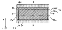
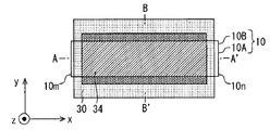
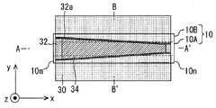
- FIG. 3A, 3B, and 3C are views showing a state before the laser chip 10 is soldered to the submount.
- FIG. 3A is a plan view. Only the outline of the laser chip 10 is drawn so that the surface of the submount can be seen.
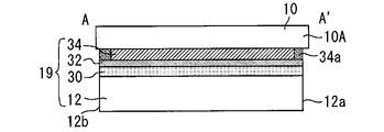
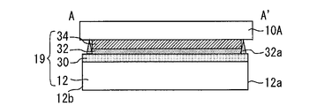
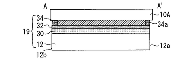
- 3B is a cross-sectional view taken along line A-A ′ of FIG. 3A.
- FIG. 3B is a cross-sectional view in the resonator direction.
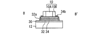
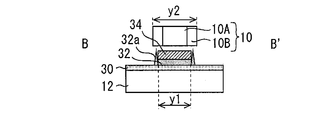
- 3C is a cross-sectional view taken along line B-B ′ of FIG. 3A.
- FIG. 3C is a cross-sectional view in a direction different from the resonator direction by 90 °.
- FIG. 3A shows that the laser chip 10 has a front end face 10n and a rear end face 10m. Although the front end surface 10n and the rear end surface 10m protrude from the submount substrate, the end surface of the submount substrate may be positioned directly below the front end surface 10n and the rear end surface 10m.
- the submount 19 will be described with reference to FIG. 3B.
- the submount 19 includes a submount substrate 12, an electrode layer 30 provided on the submount substrate 12, a barrier layer 32 provided on the electrode layer 30, a solder 34 in contact with the barrier layer 32, have.
- the material of the submount substrate 12 is, for example, SiC.
- the submount substrate 12 has a first end face 12a and a second end face 12b facing the first end face 12a.
- the electrode layer 30 is a layer provided on the laser chip 10 side of the submount substrate 12.
- the electrode layer 30 includes, for example, Ti, Ta, Mo, Pt, or Au.
- the electrode layer 30 may be formed of any one of Ti, Ta, Mo, Pt, and Au.
- the electrode layer 30 can be formed on the entire top surface of the submount substrate 12.
- the barrier layer 32 extends to a position directly above the first end face 12a and the second end face 12b.
- the barrier layer 32 is formed by depositing Pt after forming a patterned resist and then lifting off. Lift-off is a process in which Pt deposited on the resist pattern is removed together with the resist to leave the deposited Pt other than the resist pattern. At the time of lift-off, burrs 32a are generated in the barrier layer at the boundary of the pattern. Specifically, the resist shape at the time of forming the Pt pattern is set so that the burr 32a of the barrier layer 32 is generated.
- FIG. 3A shows a burr 32a.
- the burr 32 a is on the side surface of the barrier layer 32. Since the barrier layer 32 extends right above the first end surface 12a and the second end surface 12b, the burr 32a is formed above and below the barrier layer 32 in FIG. 3A and is not formed on the left and right sides of the barrier layer 32.
- the barrier layer 32 is formed so as to cover only at least one of the first end surface 12a and the second end surface 12b among the end surfaces of the submount substrate 12 in plan view.
- FIG. 3B shows that the barrier layer 32 covers the first end surface 12a and the second end surface 12b among the end surfaces of the submount substrate 12 in plan view.
- FIG. 3C shows that the barrier layer 32 does not reach the end face of the submount substrate 12. Of the end surfaces of the submount substrate 12, the barrier layer 32 does not reach the upper end surface of FIG. 3A or the lower end surface of FIG. 3A.
- the solder 34 is made of a material such as an AuSn alloy. As shown in FIG. 3A, the solder 34 is provided on the barrier layer 32 so as to recede from all end faces of the submount substrate in plan view.
- FIG. 3B shows the solder 34 provided at a position retracted from the end face of the submount 19 in the resonator direction.
- FIG. 3C shows the solder 34 provided at a position retracted from the end face of the submount substrate 12 in a direction different from the resonator direction by 90 °.
- the height of the solder burr generated by the solder cutting is as large as several tens of ⁇ m, a problem such as light being blocked by the solder burr can occur, so the solder burr is avoided.
- the height of the burr 32a of the barrier layer 32 generated by cutting the submount is as small as several ⁇ m, there is no problem even if it occurs.
- the difference between the height of the solder burr and the height of the burr 32a of the barrier layer is caused by the fact that the solder 34 is soft and extends at the time of cutting, but the Pt barrier layer 32 is hard and does not extend at the time of cutting.
- FIG. 3C shows that the burr 32 a is formed higher than the barrier layer 32.
- the solder 34 is located between the burrs 32a. Therefore, it is possible to suppress the solder 34 from spreading in a direction different by 90 ° from the resonator direction, and to secure a wire bond region where the electrode layer 30 is exposed.
- both the barrier layer 32 and the solder 34 are formed by being retracted from the end of the submount substrate 12 and the solder 32 is wetted by the burr 32a. Spread is suppressed.
- the barrier layer 32 exists up to the submount end, and the solder 34 is formed so as to be retracted inside the submount end.
- the thickness of the submount substrate 12 is 100 to 300 ⁇ m, and the thickness of the electrode layer 30 is 0.1 to 1.0 ⁇ m.
- the width of the submount substrate 12 and the electrode layer 30 is 800 to 1200 ⁇ m. The width is the length in the y direction in FIG. 3A.
- the thickness of the barrier layer 32 is 0.1 to 1.0 ⁇ m.
- the thickness of the solder 34 is 0.5 to 10 ⁇ m.
- the width of the solder 34 is 500 to 900 ⁇ m.
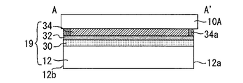
- FIG. 4A, 4B, and 4C are views showing a state after the laser chip 10 is soldered to the submount 19.
- FIG. FIG. 4A is a plan view.
- 4B is a cross-sectional view taken along line A-A ′ of FIG. 4A.
- FIG. 4B is a cross-sectional view in the resonator direction.
- 4C is a cross-sectional view taken along line B-B ′ of FIG. 4A.
- FIG. 4C is a cross-sectional view in a direction different from the resonator direction by 90 °.
- the laser chip 10 is placed on the solder 34, and the laser chip 10 is placed immediately above the first end surface 12a and directly above the second end surface 12b. Position.
- the solder 34 is heated.
- FIG. 4A shows that this heating causes the solder to spread and the extended portions 34a and 34b are formed.
- the extending portion 34a is formed by spreading solder in the direction of the resonator.
- FIG. 4B shows that the solder 34 wets and spreads in the direction of the first end surface 12a and the second end surface 12b to form the extended portion 34a, and the extended portion 34a directly connects the laser chip 10 and the barrier layer 32. ing.
- the extending portion 34a extends to the first end surface 12a and the second end surface 12b in plan view. Since the extending portion 34a connects the end of the light emitting stripe region 10A and the end of the barrier layer 32, the heat radiation property of the laser chip 10 is improved. Providing the extended portion 34a itself contributes to improving the heat dissipation, but when the extended portion 34a is brought into contact with the end of the laser chip 10 or in the vicinity thereof, high heat dissipation can be provided. In FIG. 4B, the extending portion 34a exists on both the first end surface 12a side and the second end surface 12b side, but the extending portion 34a may be provided on only one of them.
- the extending portion 34b is formed by the solder 34 being advanced along the laser chip 10 in the positive z direction of FIG. 4A.
- the spread of the solder 34 in the y positive and negative directions is suppressed by the burr 32a.
- the heated solder 34 is wet and spread in the direction of the first end surface 12a or the second end surface 12b while being restricted by the burr 32a, and the extended portion 34a is formed by the laser.
- the chip 10 and the barrier layer 32 are directly connected.
- the barrier layer 32 of the first embodiment exists up to the submount end in the resonator direction, there is no lift-off of the barrier layer 32 in the resonator direction, and no burrs are generated. That is, there is no burr in the positive and negative x direction of the barrier layer 32. Therefore, the solder 34 wets and spreads in the direction of the resonator without being restricted by burrs, and forms the extended portion 34a.
- the extending part 34 a is in contact with the end of the laser chip 10 or the vicinity thereof, and improves the heat dissipation of the laser chip 10.
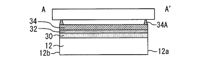
- FIG. 5A, 5B, and 5C are views showing a state after mounting the laser chip in the first comparative example.
- FIG. 5A is a plan view of the semiconductor device of the first comparative example.
- 5B is a cross-sectional view taken along line A-A ′ of FIG. 5A.
- FIG. 5C is a cross-sectional view taken along line B-B ′ of FIG. 5A.
- 5A and 5B show that the solder 34 extends right above the end face of the submount 19. In this case, solder burrs 34A are generated when the submount is cut, and the characteristics may be deteriorated or the reliability may be lowered.
- FIG. 6A, 6B, and 6C are views showing a state after mounting the laser chip in the second comparative example.
- FIG. 6A is a plan view of a semiconductor device of a second comparative example.
- 6B is a cross-sectional view taken along line A-A ′ of FIG. 6A.
- 6C is a cross-sectional view taken along the line B-B 'of FIG. 6A.
- FIG. 6A shows that the solder 34 is provided only at a position retracted from the end of the submount substrate.
- FIG. 6B shows that the solder 34 is sandwiched between two burrs 32a in the resonator direction. In this case, wetting and spreading of the solder 34 in the resonator direction is suppressed, and the solder cannot be brought into contact with the end of the laser chip or in the vicinity thereof.
- the solder 34 is retracted from all the end faces of the submount 19 and the wetting and spreading direction of the solder 34 is controlled by the burrs 32a of the barrier layer 32.
- the problem of the comparative example and the second comparative example does not occur.
- the semiconductor device manufacturing method of the present embodiment can be variously modified without losing its characteristics. All the specific materials and values described above are exemplary.
- the submount substrate 12 is described as being composed of SiC
- the solder 34 is composed of an alloy of Au and Sn
- the electrode layer 30 is composed of Ti, Ta, Mo, Pt, Au, etc., but another material is used. May be.
- the material of the barrier layer 32 is Pt
- a barrier layer other than Pt can be used as long as burrs are formed as a final structure. For example, Ni, Cu, Pd, Co or the like may be used in addition to Pt.
- the modification described in the first embodiment can be applied to a method for manufacturing a semiconductor device according to the following embodiment. Since the semiconductor device manufacturing method according to the following embodiment has many similarities to the first embodiment, the differences from the first embodiment will be mainly described.
- FIG. 7A, 7B, and 7C are views showing a state before the laser chip 10 is soldered to the submount 19.
- FIG. 7A is a plan view.
- FIG. 7B is a cross-sectional view taken along line AA ′ of FIG. 7A.
- FIG. 7B is a cross-sectional view in the resonator direction.
- FIG. 7C is a cross-sectional view taken along line BB ′ of FIG. 7A.
- FIG. 7C is a cross-sectional view in a direction different from the resonator direction by 90 °.
- the direction orthogonal to the resonator direction of the laser chip 10 is referred to as an orthogonal direction.
- the orthogonal direction is the y direction.
- the length of the barrier layer 32 and the solder 34 in the orthogonal direction is set to be shorter than the length of the laser chip 10 in the orthogonal direction.
- FIG. 7C shows that the length y1 of the barrier layer 32 and the solder 34 in the orthogonal direction is equal to or shorter than the length y2 of the laser chip 10 in the orthogonal direction.
- FIG. 8A, 8B, and 8C are views showing a state after the laser chip 10 is soldered to the submount 19.
- FIG. FIG. 8A is a plan view.
- 8B is a cross-sectional view taken along line A-A ′ of FIG. 8A.
- FIG. 8B is a cross-sectional view in the resonator direction.
- 8C is a cross-sectional view taken along line B-B ′ of FIG. 8A.
- FIG. 8C is a cross-sectional view in a direction different from the resonator direction by 90 °.
- the length of the solder 34 in the orthogonal direction to be equal to or less than the length of the laser chip 10
- wetting and spreading of the solder 34 in the orthogonal direction can be suppressed. Therefore, it is possible to make the solder 34 wet and spread more easily on the front end face 10n or the rear end face 10m side of the laser chip 10 than in the first embodiment.
- FIG. 9A, 9B, and 9C are views showing a state before the laser chip 10 is soldered to the submount 19.
- FIG. 9A is a plan view.
- FIG. 9B is a cross-sectional view taken along line AA ′ of FIG. 9A.
- FIG. 9B is a cross-sectional view in the resonator direction.
- FIG. 9C is a sectional view taken along line BB ′ of FIG. 9A.
- FIG. 9C is a cross-sectional view in a direction different from the resonator direction by 90 °.
- the y direction in FIG. 9A is the orthogonal direction defined earlier.
- the length of the solder 34 in the orthogonal direction is smaller on the front end surface 10n side than on the rear end surface 10m side.
- the side surface of the solder 34 is inclined with respect to the resonator direction in plan view.
- the solder 34 has a tapered shape whose width decreases toward the front end face 10n side.
- the orthogonal length of the solder 34 on the front end face 10n side is set to be equal to or smaller than the width of the light emitting stripe region 10A
- the orthogonal length of the solder 34 on the rear end face 10m side is set to be equal to or larger than the width of the light emitting stripe region 10A. it can.
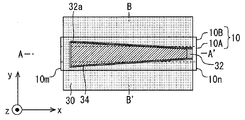
- FIG. 10A, 10B, and 10C are views showing a state after the laser chip 10 is soldered to the submount 19.
- FIG. FIG. 10A is a plan view.
- 10B is a cross-sectional view taken along line A-A ′ of FIG. 10A.
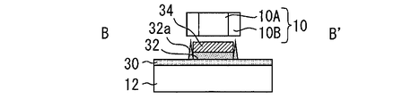
- 10C is a cross-sectional view taken along line B-B ′ of FIG. 10A.
- the length of the solder 34 in the orthogonal direction is made smaller on the front end face 12n side than on the rear end face 12m side, so that the solder 34 is easily spread in the direction of the front end face 10n. Therefore, the front end face 10n side of the laser chip and the barrier layer 32 can be connected by the extending portion 34a, so that it is possible to improve the characteristics by improving the heat dissipation on the front end face 10n of the laser chip 10.
- the length in the orthogonal direction of the solder is shortened on the front end face 10n side of the laser chip 10, but conversely, the length in the orthogonal direction of the solder 34 is shortened on the rear end face 10m side of the laser chip 10. May be.
- the extending part 34a can connect the rear end face 10m side of the laser chip 10 and the barrier layer 32, the heat dissipation on the rear end face 10m side can be improved. Therefore, the length of the solder 34 in the orthogonal direction may be reduced as it proceeds from one of the first end surface 12a side and the second end surface 12b side to the other.
- the length in the orthogonal direction at one end of the solder 34 is shorter than the length in the orthogonal direction of the light emitting stripe region 10A, and the length in the orthogonal direction is longer than the length in the orthogonal direction of the light emitting stripe region 10A at the other end of the solder 34.
- the formation of the extending portion 34a toward the front end surface 10n or the rear end surface 10m can be promoted.
- FIG. 11A, 11B, and 11C are views showing a state before the laser chip 10 is soldered to the submount 19.
- FIG. 11A is a plan view.
- FIG. 11B is a cross-sectional view taken along line AA ′ of FIG. 11A.
- FIG. 11B is a cross-sectional view in the resonator direction.
- FIG. 11C is a cross-sectional view taken along line BB ′ of FIG. 11A.
- FIG. 11C is a cross-sectional view in a direction different from the resonator direction by 90 °.
- the barrier layer 32 extends only to the first end surface 12a among the end surfaces of the submount substrate 12 in plan view. Therefore, there is a burr 32a between the second end face 12b and the barrier layer 32 as well as in the positive and negative directions of the barrier layer 32 and the solder 34 in plan view.
- the barrier layer 32 exists up to the submount end in the resonator direction, and the solder 34 is provided inside the submount end in the resonator direction.
- both the barrier layer 32 and the solder 34 are provided inside the submount end.
- FIG. 11B shows that the barrier layer 32 extends right above the first end face 12a.
- a burr 32a is formed between the barrier layer 32 and the second end face 12b. The burr 32a prevents the solder 34 from spreading in the direction of the rear end face 10m. Therefore, the solder 34 tends to wet and spread in the direction of the front end face 10n.
- FIG. 12A, 12B, and 12C are views showing a state after the laser chip 10 is soldered to the submount 19.
- FIG. FIG. 12A is a plan view.
- 12B is a cross-sectional view taken along line A-A ′ of FIG. 12A.
- 12C is a cross-sectional view taken along line B-B ′ of FIG. 12A.
- the burr 32a since the burr 32a is formed on the rear end surface 10m side of the barrier layer 32, the burr 32a prevents the solder 34 from spreading toward the rear end surface 10m. Then, wetting and spreading of the solder 34 toward the front end face 10n side is promoted, and an extended portion 34a is formed.
- the solder 34 is provided so that the length in the orthogonal direction becomes shorter as it goes to the front end face 10n side, the wetting and spreading of the solder 34 to the front end face 10n side is further promoted.
Landscapes
- Physics & Mathematics (AREA)
- Condensed Matter Physics & Semiconductors (AREA)
- General Physics & Mathematics (AREA)
- Electromagnetism (AREA)
- Optics & Photonics (AREA)
- Semiconductor Lasers (AREA)
Abstract
第1端面と第2端面とを有するサブマウント基板と、該サブマウント基板の上に設けられた電極層と、該電極層の上に設けられ平面視で該サブマウント基板の端面のうち該第1端面又は該第2端面の少なくとも一方にのみ及ぶバリア層と、該バリア層の側面にあり該バリア層より高いバリと、該バリア層の上に平面視で該サブマウント基板のすべての端面から後退して設けられた半田と、を有するサブマウントを用意することと、発光ストライプ領域と隣接領域とを有するレーザチップを、該半田の上にのせ、該第1端面の直上と該第2端面の直上に該レーザチップを位置させることと、加熱された該半田が、該バリによって濡れ広がりの制限を受けつつ、該第1端面又は該第2端面の方向に濡れ広がって延伸部を形成し、該延伸部が該レーザチップと該バリア層を直接接続することと、を備える。
Description
この発明は半導体装置の製造方法に関する。
周知の光モジュールでは、サブマウント電極と、例えばAuSnを材料とする半田との間にバリア層を設けることにより半田の広がりを抑制している。バリア層の材料はPtである。半田の濡れ広がりを抑制する効果は、バリア層により半田とサブマウント電極のAuの反応を防ぐことで得られる。加えて、Ptパターン形成時のリフトオフの際に発生したバリが障壁となり半田の広がりを防いでいることも考えられる。バリア層を設けることにより半田の広がりを抑制することで、半田がサブマウント全体に濡れ広がってワイヤボンド領域が確保できなくなることを防止できる。
特許文献1には、AuSn半田層の溶融に際して、バリア層であるPt層の存在によりAu層と反応せずはんだとしての性質を保つことが開示されている。
サブマウントの端、つまり、切断ラインまで半田が存在すると、切断時に半田バリが発生し、特性悪化及び信頼性低下につながる可能性がある。これを防ぐため、半田をサブマウントの端より内側に引っ込めて形成する必要がある。つまり、半田をサブマウントの端面より後退させたい場所にだけ設ける。このように用意したサブマウントにレーザチップを半田付けする際、レーザチップの下で押された半田は、半田の存在する領域である共振器とは90°異なる方向に進みやすく、半田の存在しない共振器方向には進みにくい。そのためレーザチップの端面は半田が濡れにくく放熱性が悪い問題があった。
本発明は上述の問題を解決するためになされたものであり、ワイヤボンド領域を確保するため共振器とは90°異なる方向には半田の濡れ広がりを抑制しつつ、放熱性を向上させるためサブマウントの端またはその近傍まで半田が濡れ易い半導体装置の製造方法を提供することを目的とする。
本願の発明にかかる半導体装置の製造方法は、第1端面と該第1端面に対向する第2端面とを有するサブマウント基板と、該サブマウント基板の上に設けられた電極層と、該電極層の上に設けられ、平面視で該サブマウント基板の端面のうち該第1端面又は該第2端面の少なくとも一方にのみ及ぶバリア層と、該バリア層の側面にあり該バリア層より高いバリと、該バリア層の上に平面視で該サブマウント基板のすべての端面から後退して設けられた半田と、を有するサブマウントを用意することと、発光ストライプ領域と、該発光ストライプ領域の左右の隣接領域と、を有するレーザチップを、該半田の上にのせ、該第1端面の直上と該第2端面の直上に該レーザチップを位置させることと、加熱された該半田が、該バリによって濡れ広がりの制限を受けつつ、該第1端面又は該第2端面の方向に濡れ広がって延伸部を形成し、該延伸部が該レーザチップと該バリア層を直接接続することと、を備えたことを特徴とする。
本発明のその他の特徴は以下に明らかにする。
溶融した半田の延伸方向をバリア層のバリによって制限し、半田をレーザチップの前端面側又は後端面側に延伸させるので、ワイヤボンド領域を確保しつつ、サブマウントの端またはその近傍まで半田を濡れ広げることができる。
実施の形態に係る半導体装置の製造方法について図面を参照して説明する。同じ又は対応する構成要素には同じ符号を付し、説明の繰り返しを省略する場合がある。
実施の形態1.
図1は、実施の形態1の半導体装置の斜視図である。少なくとも一部が半導体で形成されたレーザチップ10はサブマウント19に実装されている。サブマウント19はヒートシンク14に実装されている。ヒートシンク14はステム16に固定されている。ステム16を貫通する端子18が複数設けられている。この端子18とレーザチップ10が電気的に接続されている。例えば、レーザチップ10の上面と端子18がワイヤで接続され、サブマウント19と別の端子18が別のワイヤで接続される。
図1は、実施の形態1の半導体装置の斜視図である。少なくとも一部が半導体で形成されたレーザチップ10はサブマウント19に実装されている。サブマウント19はヒートシンク14に実装されている。ヒートシンク14はステム16に固定されている。ステム16を貫通する端子18が複数設けられている。この端子18とレーザチップ10が電気的に接続されている。例えば、レーザチップ10の上面と端子18がワイヤで接続され、サブマウント19と別の端子18が別のワイヤで接続される。
図2は、レーザチップ10をレーザの進行方向に対し垂直に切断した断面図である。レーザチップ10は半導体基板10aを有している。この半導体基板10aの上には、n型のAlInPからなる下クラッド層10bが形成されている。半導体基板10aと下クラッド層10bは直接接合している。下クラッド層10bの上にはアンドープのAlInPからなる下光ガイド層10cが形成されている。下光ガイド層10cの上にはGaInPからなる活性層10dが形成されている。
活性層10dの上にはアンドープのAlGaInPからなる上光ガイド層10eが形成されている。上光ガイド層10eの上にはp型のAlInPからなる上クラッド層10fが形成されている。上クラッド層10fの上にはp型のGaAsからなるコンタクト層10gが形成されている。
半導体基板10aの厚さは50~150μmである。下クラッド層10bの厚さは0.5~4.0μmである。下クラッド層10bのキャリア濃度は0.5~1.5×1018cm-3である。下光ガイド層10cおよび上光ガイド層10eの厚さは0.02~0.4μmである。活性層10dの厚さは3.0~20nmである。上クラッド層10fの厚さは0.5~4.0μmである。上クラッド層10fのキャリア濃度は0.5~2.0×1018cm-3である。コンタクト層10gの厚さは0.05~0.5μmである。コンタクト層10gのキャリア濃度は1.0~4.0×1019cm-3である。
コンタクト層10gの横にはシリコン窒化膜などの絶縁膜10hが形成されている。発光領域すなわち電流が注入される領域ではこの絶縁膜10hがエッチングされて開口を持つようになっている。この開口部以外のコンタクト層はエッチングにより除去されている。コンタクト層10gおよび絶縁膜10hの上にはp側電極10iが形成されている。p側電極10iはTi、Pt、Auなどの薄膜を積層したものである。p側電極10iの厚さは0.05~1.0μmである。絶縁膜10hの開口を通してコンタクト層10gとp側電極10iが低抵抗接合している。p側電極10iの上には金メッキ層10jが形成されている。金メッキ層10jの厚さは1.0~6.0μmである。
半導体基板10aの下面にはn側電極10kが接合されている。n側電極10kの下には金メッキ層10lが形成されている。n側電極10kはTi、Pt、Auなどの薄膜を積層したものである。n側電極10kの厚さは0.05~1.0μmであり、金メッキ層10lの厚さは1.0~6.0μmである。レーザチップ10の幅L1は400μmである。
レーザチップ10は、発光ストライプ領域10Aと、発光ストライプ領域10Aの左右の隣接領域10Bを有している。発光ストライプ領域10Aは発光領域のみ残るようにエッチングされたコンタクト層10gが形成された部分である。発光ストライプ領域10Aの幅は100μmである。なお、上述の材料と数値は例示であり別の材料と数値としてもよい。以下の記述も例示であり、限定的なものではない。
このレーザチップ10は上下を反対にしてp側の金メッキ層10jがサブマウント19にダイボンドされる。そして、金メッキ層10lにワイヤボンドし、そのワイヤを介してレーザチップ10に電流供給される。
図3A、3B、3Cはレーザチップ10をサブマウントに半田付けする前の状態を示す図である。図3Aは平面図である。サブマウントの表面が見えるようにレーザチップ10については輪郭のみが描かれている。図3Bは図3AのA-A’線における断面図である。図3Bは共振器方向の断面図となっている。図3Cは図3AのB-B’線における断面図である。図3Cは共振器方向とは90°異なる方向の断面図となっている。
図3Aにはレーザチップ10が前端面10nと後端面10mを有することが示されている。前端面10nと後端面10mはサブマウント基板よりも突出しているが、前端面10nと後端面10mの直下にサブマウント基板の端面が位置するようにしてもよい。
図3Bを参照してサブマウント19について説明する。サブマウント19は、サブマウント基板12と、サブマウント基板12の上に設けられた電極層30と、電極層30の上に設けられたバリア層32と、バリア層32に接した半田34と、を有している。
サブマウント基板12の材料は例えばSiCである。サブマウント基板12は第1端面12aと第1端面12aに対向する第2端面12bとを有する。電極層30はサブマウント基板12のレーザチップ10側に設けた層である。電極層30は例えば、Ti、Ta、Mo、Pt又はAuを含む。Ti、Ta、Mo、Pt、Auのいずれか1つで電極層30を形成してもよい。電極層30はサブマウント基板12の上面全体に形成することができる。
バリア層32は、図3Bに示されるように第1端面12aと第2端面12bの直上まで及んでいる。バリア層32は、パターニングされたレジストを形成した後に、Ptを蒸着し、その後、リフトオフすることで形成する。リフトオフとはレジストパターン上に蒸着されたPtをレジストごと除去することにより、レジストパターン以外に蒸着されたPtを残す工程である。このリフトオフの際、パターンの境目のバリア層にバリ32aが発生する。具体的には、バリア層32のバリ32aが発生するように、Ptパターン形成時のレジスト形状を設定する。レジスト厚が厚すぎる場合はレジストが影となり、パターンの境目のレジストの側面にPtが蒸着されないためバリは発生しない。また、レジスト厚が薄すぎる場合はパターンの境目のレジストの側面にPtが蒸着されるが、レジストパターン以外に蒸着されたPtと、レジスト側面に蒸着されたPtと、レジストパターン上に蒸着されたPtとが繋がってしまうためリフトオフができない。そのため、レジスト厚をPtの厚みの1.5倍以上から4倍以下、より好ましくは2倍以上から3倍以下とすることでバリを形成しつつリフトオフが可能となる。
図3Aにはバリ32aが示されている。このバリ32aはバリア層32の側面にある。バリア層32は第1端面12aと第2端面12bの直上まで及んでいるので、バリ32aは、図3Aにおいてバリア層32の上下に形成されバリア層32の左右に形成されない。バリア層32は、平面視でサブマウント基板12の端面のうち第1端面12a又は第2端面12bの少なくとも一方にのみに及ぶように形成される。図3Bにはバリア層32が、平面視でサブマウント基板12の端面のうち第1端面12aと第2端面12bに及ぶことが示されている。図3Cにはバリア層32がサブマウント基板12の端面に及んでいないことが示されている。バリア層32は、サブマウント基板12の端面のうち、図3Aの上側の端面にも図3Aの下側の端面にも及ばない。
半田34は、例えばAuSn合金などの材料で形成されている。図3Aに示されているように、半田34はバリア層32の上に平面視でサブマウント基板のすべての端面から後退して設けられている。図3Bには、共振器方向についてサブマウント19の端面から後退した位置に設けられた半田34が示されている。図3Cには、共振器方向と90°異なる方向についてサブマウント基板12の端面から後退した位置に設けられた半田34が示されている。サブマウント基板の端面から後退した位置に半田34を設けることで、サブマウント切断時の半田バリを防ぐことができる。半田切断により生じる半田バリの高さは数十μmと大きいため半田バリによって光が遮られるなどの不具合が生じえるので、半田バリは回避する。これに対し、サブマウント切断により生じるバリア層32のバリ32aの高さは数μmと微小であるため、発生しても問題ない。半田バリの高さと、バリア層のバリ32aの高さの違いは、半田34は柔らかいため切断時に延びるが、Ptのバリア層32は固いため切断時に延びないことが原因で生じる。
図3Cには、バリ32aがバリア層32より高く形成されたことが示されている。図3Cにおいて、半田34はこのバリ32aに挟まれた位置にある。そのため、半田34が共振器方向とは90°異なる方向へ濡れ広がることが抑制され、電極層30が露出したワイヤボンド領域を確保することができる。このように、共振器方向と90°異なる方向であるy方向については、バリア層32と半田34の両方が、サブマウント基板12の端から内側に引っ込めて形成され、しかもバリ32aによって半田の濡れ広がりが抑制されている。共振器方向であるx方向について言えば、バリア層32はサブマウント端まで存在し、半田34はサブマウント端より内側に引っ込めて形成している。
サブマウント基板12の厚みは100~300μmであり、電極層30の厚みは0.1~1.0μmである。サブマウント基板12と電極層30の幅は800~1200μmである。幅とは、図3Aのy方向の長さのことである。バリア層32の厚みは0.1~1.0μmである。半田34の厚さは0.5~10μmである。半田34の幅は500~900μmである。
実施の形態1の半導体装置の製造方法ではまずこのようなサブマウント19を用意する。図3B、3C、3Dには、サブマウント19の上にレーザチップ10がのせられる直前の状態が示されている。
図4A、4B、4Cは、レーザチップ10をサブマウント19に半田付けした後の状態を示す図である。図4Aは平面図である。図4Bは図4AのA-A’線における断面図である。図4Bは共振器方向の断面図となっている。図4Cは図4AのB-B’線における断面図である。図4Cは共振器方向とは90°異なる方向の断面図となっている。
実施の形態1に係る半導体装置の製造方法では、図4Bに示されるように、レーザチップ10を半田34の上にのせ、第1端面12aの直上と第2端面12bの直上にレーザチップ10を位置させる。次いで、半田34を加熱する。図4Aには、この加熱により半田が濡れ広がって延伸部34a、34bが形成されたことが示されている。延伸部34aは半田が共振器方向に濡れ広がって形成される。図4Bには、半田34が第1端面12aと第2端面12bの方向に濡れ広がって延伸部34aを形成し、その延伸部34aがレーザチップ10とバリア層32を直接接続することが示されている。延伸部34aは平面視で第1端面12aと第2端面12bに及ぶ。延伸部34aは、発光ストライプ領域10Aの端部とバリア層32の端部とを接続するので、レーザチップ10の放熱性を高めるものである。延伸部34aを設けること自体が放熱性改善に寄与するが、この延伸部34aをレーザチップ10の端又はその近くに接触させると高い放熱性を提供できる。図4Bでは第1端面12a側と第2端面12b側の両方に延伸部34aが存在するが、どちらか一方だけに延伸部34aがあってもよい。
延伸部34bは、半田34がレーザチップ10に沿って図4Aのz正方向に進んで形成されたものである。図4Aにおいて、半田34のy正負方向への塗れ広がりはバリ32aによって抑制される。このように、加熱された半田34が、バリ32aによって濡れ広がりの制限を受けつつ、第1端面12a又は第2端面12bの方向に濡れ広がって延伸部34aを形成し、その延伸部34aがレーザチップ10とバリア層32を直接接続する。
実施の形態1のバリア層32は共振器方向のサブマウント端まで存在するので、共振器方向のバリア層32のリフトオフはなく、バリは発生しない。つまり、バリア層32のx正負方向にはバリがない。そのため、半田34は、バリによる制限を受けることなく共振器方向に濡れ広がり、延伸部34aを形成する。延伸部34aは、レーザチップ10の端又はその近傍に接し、レーザチップ10の放熱性を高める。
ここで、第1比較例について説明する。図5A、5B、5Cは第1比較例におけるレーザチップ実装後の状態を示す図である。図5Aは第1比較例の半導体装置の平面図である。図5Bは図5AのA-A’線における断面図である。図5Cは図5AのB-B’線における断面図である。図5A、5Bには半田34がサブマウント19の端面直上に及んでいることが示されている。この場合、サブマウントの切断時に半田バリ34Aが発生し、特性が悪化したり信頼性が低下したりする可能性がある。
次いで、第2比較例について説明する。図6A、6B、6Cは第2比較例におけるレーザチップ実装後の状態を示す図である。図6Aは第2比較例の半導体装置の平面図である。図6Bは図6AのA-A’線における断面図である。図6Cは図6AのB-B’線における断面図である。図6Aには半田34がサブマウント基板の端から後退した位置にのみ設けられたことが示されている。図6Bには、共振器方向において半田34が2つのバリ32aで挟まれていることが示されている。この場合、半田34の共振器方向の濡れ広がりが抑制され、レーザチップの端又はその近傍に半田を接触させることができない。
本実施形態の半導体装置の製造方法では、上述のとおり、半田34をサブマウント19のすべての端面から後退させ、バリア層32のバリ32aによって半田34の濡れ広がり方向をコントロールすることで、第1比較例と第2比較例の問題は生じない。
本実施形態の半導体装置の製造方法は、その特徴を失わない範囲で様々な変形が可能である。上述の具体的な材料および数値はすべて例示である。例えば、本実施形態では、サブマウント基板12をSiC、半田34をAuとSnの合金、電極層30をTi、Ta、Mo、Pt、Auなどからなるものとして説明したが、別の材料を用いてもよい。また、バリア層32の材料はPtとしたが、最終構造としてバリが形成されるものであればPt以外のバリア層を用いることができる。Pt以外に例えば、Ni、Cu、Pd、Coなどでもよい。
実施の形態1で説明した変形は以下の実施の形態に係る半導体装置の製造方法に応用することができる。なお、以下の実施の形態に係る半導体装置の製造方法は実施の形態1との類似点が多いので実施の形態1との相違点を中心に説明する。
実施の形態2.
実施の形態2は、図7A、7B、7Cと図8A、8B、8Cを参照して説明する。図7A、7B、7Cはレーザチップ10をサブマウント19に半田付けする前の状態を示す図である。図7Aは平面図である。図7Bは図7AのA-A’線における断面図である。図7Bは共振器方向の断面図となっている。図7Cは図7AのB-B’線における断面図である。図7Cは共振器方向とは90°異なる方向の断面図となっている。
実施の形態2は、図7A、7B、7Cと図8A、8B、8Cを参照して説明する。図7A、7B、7Cはレーザチップ10をサブマウント19に半田付けする前の状態を示す図である。図7Aは平面図である。図7Bは図7AのA-A’線における断面図である。図7Bは共振器方向の断面図となっている。図7Cは図7AのB-B’線における断面図である。図7Cは共振器方向とは90°異なる方向の断面図となっている。
レーザチップ10の共振器方向と直交する方向を直交方向という。直交方向はy方向である。実施の形態2では、直交方向のバリア層32および半田34の長さを、直交方向のレーザチップ10の長さ以下とした。図7Cには、直交方向のバリア層32および半田34の長さy1を、直交方向のレーザチップ10の長さy2以下としたことが示されている。
図8A、8B、8Cはレーザチップ10をサブマウント19に半田付けした後の状態を示す図である。図8Aは平面図である。図8Bは図8AのA-A’線における断面図である。図8Bは共振器方向の断面図となっている。図8Cは図8AのB-B’線における断面図である。図8Cは共振器方向とは90°異なる方向の断面図となっている。上述のとおり、直交方向の半田34の長さをレーザチップ10の長さ以下とすることにより、直交方向への半田34の濡れ広がりを抑制できる。そのため、実施の形態1よりもレーザチップ10の前端面10n又は後端面10m側に半田34を濡れ広がりやすくすることができる。
実施の形態3.
実施の形態3は、図9A、9B、9Cと図10A、10B、10Cを参照して説明する。図9A、9B、9Cはレーザチップ10をサブマウント19に半田付けする前の状態を示す図である。図9Aは平面図である。図9Bは図9AのA-A’線における断面図である。図9Bは共振器方向の断面図となっている。図9Cは図9AのB-B’線における断面図である。図9Cは共振器方向とは90°異なる方向の断面図となっている。
実施の形態3は、図9A、9B、9Cと図10A、10B、10Cを参照して説明する。図9A、9B、9Cはレーザチップ10をサブマウント19に半田付けする前の状態を示す図である。図9Aは平面図である。図9Bは図9AのA-A’線における断面図である。図9Bは共振器方向の断面図となっている。図9Cは図9AのB-B’線における断面図である。図9Cは共振器方向とは90°異なる方向の断面図となっている。
図9Aのy方向が先ほど定義した直交方向である。実施の形態3では、後端面10m側より前端面10n側で直交方向の半田34の長さが小さい。例えば、半田34の側面は平面視で共振器方向に対して傾斜している。言いかえれば半田34は、前端面10n側に向かって幅が小さくなっていく先細りの形状となっている。さらに、例えば、前端面10n側の半田34の直交方向長さは発光ストライプ領域10Aの幅以下とし、後端面10m側の半田34の直交方向長さは発光ストライプ領域10Aの幅以上とすることができる。
図10A、10B、10Cはレーザチップ10をサブマウント19に半田付けした後の状態を示す図である。図10Aは平面図である。図10Bは図10AのA-A’線における断面図である。図10Cは図10AのB-B’線における断面図である。前述のとおり、半田34の直交方向長さを前端面12n側で後端面12m側より小さくしたことにより、半田34は前端面10nの方向に濡れ広がりやすくなっている。そのため、延伸部34aによってレーザチップの前端面10n側とバリア層32を接続できるので、レーザチップ10の前端面10nにおける放熱性向上による特性改善が可能となる。
実施の形態3では、レーザチップ10の前端面10n側で半田の直交方向の長さを短くしたが、逆に、レーザチップ10の後端面10m側で半田34の直交方向の長さを短くしてもよい。この場合は、延伸部34aによってレーザチップ10の後端面10m側とバリア層32を接続できるので、後端面10m側の放熱性を高めることができる。したがって、直交方向の半田34の長さは、第1端面12a側と第2端面12b側の一方から他方に進むほど小さくすればよい。そして、半田34の一端では直交方向の長さが発光ストライプ領域10Aの直交方向の長さより短く、半田34の他端では直交方向の長さが発光ストライプ領域10Aの直交方向の長さより長くすれば、前端面10n又は後端面10m側への延伸部34aの形成を促進できる。
実施の形態4.
実施の形態4は、図11A、11B、11Cと図12A、12B、12Cを参照して説明する。図11A、11B、11Cはレーザチップ10をサブマウント19に半田付けする前の状態を示す図である。図11Aは平面図である。図11Bは図11AのA-A’線における断面図である。図11Bは共振器方向の断面図となっている。図11Cは図11AのB-B’線における断面図である。図11Cは共振器方向とは90°異なる方向の断面図となっている。
実施の形態4は、図11A、11B、11Cと図12A、12B、12Cを参照して説明する。図11A、11B、11Cはレーザチップ10をサブマウント19に半田付けする前の状態を示す図である。図11Aは平面図である。図11Bは図11AのA-A’線における断面図である。図11Bは共振器方向の断面図となっている。図11Cは図11AのB-B’線における断面図である。図11Cは共振器方向とは90°異なる方向の断面図となっている。
図11A、11Bに示すように、バリア層32は平面視でサブマウント基板12の端面のうち第1端面12aのみに及んでいる。そのため、平面視でバリア層32と半田34のy正負方向だけでなく、第2端面12bとバリア層32の間にもバリ32aがある。このように、前端面10n側については、バリア層32が共振器方向のサブマウント端まで存在し、半田34は共振器方向のサブマウント端より内側に設けられている。一方、後端面10m側については、バリア層32と半田34が両方ともサブマウント端より内側に設けられている。
図11Bには、バリア層32が第1端面12aの直上に及んだことが示されている。また、バリア層32と第2端面12bの間にはバリ32aが形成されている。このバリ32aは、半田34が後端面10mの方向に濡れ広がることを抑制する。よって、前端面10nの方向に半田34が濡れ広がりやすくなる。
図12A、12B、12Cはレーザチップ10をサブマウント19に半田付けした後の状態を示す図である。図12Aは平面図である。図12Bは図12AのA-A’線における断面図である。図12Cは図12AのB-B’線における断面図である。前述のとおり、バリア層32の後端面10m側にバリ32aを形成したので、このバリ32aによって半田34が後端面10mの方に濡れ広がることが抑制される。そして、前端面10n側への半田34の濡れ広がりが促進され延伸部34aができる。また、実施の形態3で説明したとおり、前端面10n側に進むほど直交方向の長さが短くなるように半田34を設ければ、さらに前端面10n側への半田34の濡れ広がりが促進される。
なお、上記の各実施の形態の特徴を組み合わることができる。
10 レーザチップ、 12 サブマウント基板、 19 サブマウント、 30 電極層、 32 バリア層、 34 半田
Claims (8)
- 第1端面と前記第1端面に対向する第2端面とを有するサブマウント基板と、前記サブマウント基板の上に設けられた電極層と、前記電極層の上に設けられ、平面視で前記サブマウント基板の端面のうち前記第1端面又は前記第2端面の少なくとも一方にのみ及ぶバリア層と、前記バリア層の側面にあり前記バリア層より高いバリと、前記バリア層の上に平面視で前記サブマウント基板のすべての端面から後退して設けられた半田と、を有するサブマウントを用意することと、
発光ストライプ領域と、前記発光ストライプ領域の左右の隣接領域と、を有するレーザチップを、前記半田の上にのせ、前記第1端面の直上と前記第2端面の直上に前記レーザチップを位置させることと、
加熱された前記半田が、前記バリによって濡れ広がりの制限を受けつつ、前記第1端面又は前記第2端面の方向に濡れ広がって延伸部を形成し、前記延伸部が前記レーザチップと前記バリア層を直接接続することと、を備えた半導体装置の製造方法。 - 前記バリア層は、平面視で前記第1端面と前記第2端面に及び、前記延伸部は平面視で前記第1端面と前記第2端面に及ぶことを特徴とする請求項1に記載の半導体装置の製造方法。
- 前記レーザチップの共振器方向と直交する方向である直交方向の前記バリア層および前記半田の長さは、前記直交方向の前記レーザチップの長さ以下であることを特徴とする請求項1又は2に記載の半導体装置の製造方法。
- 前記レーザチップの共振器方向と直交する方向である直交方向の前記半田の長さは、前記第1端面側と前記第2端面側の一方から他方に進むほど小さくなること特徴とする請求項1又は2に記載の半導体装置の製造方法。
- 前記半田の一端では前記直交方向の長さが前記発光ストライプ領域の前記直交方向の長さより短く、前記半田の他端では前記直交方向の長さが前記発光ストライプ領域の前記直交方向の長さより長いことを特徴とする請求項4に記載の半導体装置の製造方法。
- 前記バリア層は平面視で前記サブマウント基板の端面のうち前記第1端面のみに及び、平面視で前記第2端面と前記バリア層の間には前記バリがあることを特徴とする請求項1に記載の半導体装置の製造方法。
- 前記半田は、前記第1端面側に進むほど、前記レーザチップの共振器方向と直交する方向である直交方向の長さが短くなることを特徴とする請求項6に記載の半導体装置の製造方法。
- 前記バリア層はリフトオフ法によって形成され、リフトオフの際に前記バリが生じることを特徴とする請求項1から7のいずれか1項に記載の半導体装置の製造方法。
Priority Applications (4)
| Application Number | Priority Date | Filing Date | Title |
|---|---|---|---|
| US16/965,578 US11411369B2 (en) | 2018-04-03 | 2018-04-03 | Method for manufacturing semiconductor device |
| PCT/JP2018/014216 WO2019193643A1 (ja) | 2018-04-03 | 2018-04-03 | 半導体装置の製造方法 |
| CN201880091961.4A CN111937257B (zh) | 2018-04-03 | 2018-04-03 | 半导体装置的制造方法 |
| JP2018545400A JP6512375B1 (ja) | 2018-04-03 | 2018-04-03 | 半導体装置の製造方法 |
Applications Claiming Priority (1)
| Application Number | Priority Date | Filing Date | Title |
|---|---|---|---|
| PCT/JP2018/014216 WO2019193643A1 (ja) | 2018-04-03 | 2018-04-03 | 半導体装置の製造方法 |
Publications (1)
| Publication Number | Publication Date |
|---|---|
| WO2019193643A1 true WO2019193643A1 (ja) | 2019-10-10 |
Family
ID=66530725
Family Applications (1)
| Application Number | Title | Priority Date | Filing Date |
|---|---|---|---|
| PCT/JP2018/014216 Ceased WO2019193643A1 (ja) | 2018-04-03 | 2018-04-03 | 半導体装置の製造方法 |
Country Status (4)
| Country | Link |
|---|---|
| US (1) | US11411369B2 (ja) |
| JP (1) | JP6512375B1 (ja) |
| CN (1) | CN111937257B (ja) |
| WO (1) | WO2019193643A1 (ja) |
Families Citing this family (1)
| Publication number | Priority date | Publication date | Assignee | Title |
|---|---|---|---|---|
| WO2021186695A1 (ja) * | 2020-03-19 | 2021-09-23 | 三菱電機株式会社 | 光半導体素子 |
Citations (3)
| Publication number | Priority date | Publication date | Assignee | Title |
|---|---|---|---|---|
| JP2009111080A (ja) * | 2007-10-29 | 2009-05-21 | Hitachi Kyowa Engineering Co Ltd | 電子部品搭載方法及び電子部品基板搭載構造体 |
| JP2011222675A (ja) * | 2010-04-07 | 2011-11-04 | Mitsubishi Electric Corp | 半導体装置及びその製造方法 |
| JP2015173218A (ja) * | 2014-03-12 | 2015-10-01 | 三菱電機株式会社 | 半導体レーザ光源 |
Family Cites Families (6)
| Publication number | Priority date | Publication date | Assignee | Title |
|---|---|---|---|---|
| JP3190718B2 (ja) * | 1992-01-14 | 2001-07-23 | 株式会社東芝 | 半導体レーザ用サブマウント |
| JP3346971B2 (ja) * | 1995-12-20 | 2002-11-18 | 株式会社東芝 | 光半導体素子用サブマウントおよびそのマウント方法 |
| JP3982284B2 (ja) * | 2002-03-06 | 2007-09-26 | 住友電気工業株式会社 | サブマウントおよび半導体装置 |
| JP4088867B2 (ja) * | 2002-05-01 | 2008-05-21 | 株式会社リコー | 半導体発光素子の固着方法 |
| JP4544892B2 (ja) * | 2004-03-30 | 2010-09-15 | 三洋電機株式会社 | 半導体レーザ装置およびその製造方法 |
| JP2006303299A (ja) | 2005-04-22 | 2006-11-02 | Sharp Corp | 半導体レーザ |
-
2018
- 2018-04-03 WO PCT/JP2018/014216 patent/WO2019193643A1/ja not_active Ceased
- 2018-04-03 US US16/965,578 patent/US11411369B2/en active Active
- 2018-04-03 JP JP2018545400A patent/JP6512375B1/ja active Active
- 2018-04-03 CN CN201880091961.4A patent/CN111937257B/zh active Active
Patent Citations (3)
| Publication number | Priority date | Publication date | Assignee | Title |
|---|---|---|---|---|
| JP2009111080A (ja) * | 2007-10-29 | 2009-05-21 | Hitachi Kyowa Engineering Co Ltd | 電子部品搭載方法及び電子部品基板搭載構造体 |
| JP2011222675A (ja) * | 2010-04-07 | 2011-11-04 | Mitsubishi Electric Corp | 半導体装置及びその製造方法 |
| JP2015173218A (ja) * | 2014-03-12 | 2015-10-01 | 三菱電機株式会社 | 半導体レーザ光源 |
Also Published As
| Publication number | Publication date |
|---|---|
| CN111937257A (zh) | 2020-11-13 |
| JPWO2019193643A1 (ja) | 2020-04-30 |
| CN111937257B (zh) | 2022-03-04 |
| JP6512375B1 (ja) | 2019-05-15 |
| US11411369B2 (en) | 2022-08-09 |
| US20210050706A1 (en) | 2021-02-18 |
Similar Documents
| Publication | Publication Date | Title |
|---|---|---|
| CN103975490B (zh) | 半导体激光二极管 | |
| US8442085B2 (en) | Semiconductor optical device | |
| KR101561203B1 (ko) | 반도체 발광소자 | |
| JP2011222675A (ja) | 半導体装置及びその製造方法 | |
| JP2004274057A (ja) | 半導体レーザーダイオードのサブマウント、その製造方法及びこれを採用した半導体レーザーダイオード組立体 | |
| US9692204B2 (en) | Semiconductor laser element and method of making semiconductor laser device | |
| JP2003101113A (ja) | 窒化物半導体レーザ装置 | |
| KR101638120B1 (ko) | 반도체 발광소자 | |
| JPH10223930A (ja) | 半導体発光素子 | |
| JP2007189075A (ja) | 半導体レーザ素子、半導体レーザ素子の実装構造、半導体レーザ素子の製造方法及び半導体レーザ素子の実装方法 | |
| JP6512375B1 (ja) | 半導体装置の製造方法 | |
| JP3339369B2 (ja) | レーザダイオード | |
| JP4036658B2 (ja) | 窒化物系化合物半導体レーザ装置およびその製造方法 | |
| JP3314616B2 (ja) | 大出力用半導体レーザ素子 | |
| US20210111030A1 (en) | Method of producing a semiconductor laser and semiconductor laser | |
| US20070076772A1 (en) | Semiconductor laser device | |
| JP2007027572A (ja) | 半導体発光装置およびその製造方法 | |
| JPWO2019180773A1 (ja) | 半導体装置の製造方法 | |
| JP2004055683A (ja) | 窒化物半導体レーザ素子チップとそれを含むレーザ装置 | |
| KR20150114446A (ko) | 반도체 발광소자 | |
| CN101227060A (zh) | 具有非完全粘接区域的半导体激光装置和电子设备 | |
| JP2008294421A (ja) | 半導体レーザ素子およびその製造方法 | |
| KR100922847B1 (ko) | 레이저 다이오드 및 그 제조방법 | |
| CN115917897A (zh) | 半导体激光元件的制造方法、半导体激光元件及半导体激光装置 | |
| JP4916330B2 (ja) | 窒化物半導体レーザ装置の製造方法 |
Legal Events
| Date | Code | Title | Description |
|---|---|---|---|
| ENP | Entry into the national phase |
Ref document number: 2018545400 Country of ref document: JP Kind code of ref document: A |
|
| 121 | Ep: the epo has been informed by wipo that ep was designated in this application |
Ref document number: 18913387 Country of ref document: EP Kind code of ref document: A1 |
|
| NENP | Non-entry into the national phase |
Ref country code: DE |
|
| 122 | Ep: pct application non-entry in european phase |
Ref document number: 18913387 Country of ref document: EP Kind code of ref document: A1 |