WO2019189378A1 - 窒化アルミニウム板 - Google Patents
窒化アルミニウム板 Download PDFInfo
- Publication number
- WO2019189378A1 WO2019189378A1 PCT/JP2019/013227 JP2019013227W WO2019189378A1 WO 2019189378 A1 WO2019189378 A1 WO 2019189378A1 JP 2019013227 W JP2019013227 W JP 2019013227W WO 2019189378 A1 WO2019189378 A1 WO 2019189378A1
- Authority
- WO
- WIPO (PCT)
- Prior art keywords
- aluminum nitride
- surface layer
- plane
- plate
- layer
- Prior art date
Links
Images


Classifications
-
- C—CHEMISTRY; METALLURGY
- C01—INORGANIC CHEMISTRY
- C01B—NON-METALLIC ELEMENTS; COMPOUNDS THEREOF; METALLOIDS OR COMPOUNDS THEREOF NOT COVERED BY SUBCLASS C01C
- C01B21/00—Nitrogen; Compounds thereof
- C01B21/06—Binary compounds of nitrogen with metals, with silicon, or with boron, or with carbon, i.e. nitrides; Compounds of nitrogen with more than one metal, silicon or boron
- C01B21/072—Binary compounds of nitrogen with metals, with silicon, or with boron, or with carbon, i.e. nitrides; Compounds of nitrogen with more than one metal, silicon or boron with aluminium
- C01B21/0722—Preparation by direct nitridation of aluminium
-
- C—CHEMISTRY; METALLURGY
- C04—CEMENTS; CONCRETE; ARTIFICIAL STONE; CERAMICS; REFRACTORIES
- C04B—LIME, MAGNESIA; SLAG; CEMENTS; COMPOSITIONS THEREOF, e.g. MORTARS, CONCRETE OR LIKE BUILDING MATERIALS; ARTIFICIAL STONE; CERAMICS; REFRACTORIES; TREATMENT OF NATURAL STONE
- C04B35/00—Shaped ceramic products characterised by their composition; Ceramics compositions; Processing powders of inorganic compounds preparatory to the manufacturing of ceramic products
- C04B35/515—Shaped ceramic products characterised by their composition; Ceramics compositions; Processing powders of inorganic compounds preparatory to the manufacturing of ceramic products based on non-oxide ceramics
- C04B35/58—Shaped ceramic products characterised by their composition; Ceramics compositions; Processing powders of inorganic compounds preparatory to the manufacturing of ceramic products based on non-oxide ceramics based on borides, nitrides, i.e. nitrides, oxynitrides, carbonitrides or oxycarbonitrides or silicides
- C04B35/581—Shaped ceramic products characterised by their composition; Ceramics compositions; Processing powders of inorganic compounds preparatory to the manufacturing of ceramic products based on non-oxide ceramics based on borides, nitrides, i.e. nitrides, oxynitrides, carbonitrides or oxycarbonitrides or silicides based on aluminium nitride
-
- C—CHEMISTRY; METALLURGY
- C04—CEMENTS; CONCRETE; ARTIFICIAL STONE; CERAMICS; REFRACTORIES
- C04B—LIME, MAGNESIA; SLAG; CEMENTS; COMPOSITIONS THEREOF, e.g. MORTARS, CONCRETE OR LIKE BUILDING MATERIALS; ARTIFICIAL STONE; CERAMICS; REFRACTORIES; TREATMENT OF NATURAL STONE
- C04B35/00—Shaped ceramic products characterised by their composition; Ceramics compositions; Processing powders of inorganic compounds preparatory to the manufacturing of ceramic products
- C04B35/622—Forming processes; Processing powders of inorganic compounds preparatory to the manufacturing of ceramic products
- C04B35/626—Preparing or treating the powders individually or as batches ; preparing or treating macroscopic reinforcing agents for ceramic products, e.g. fibres; mechanical aspects section B
- C04B35/62605—Treating the starting powders individually or as mixtures
- C04B35/62645—Thermal treatment of powders or mixtures thereof other than sintering
- C04B35/6265—Thermal treatment of powders or mixtures thereof other than sintering involving reduction or oxidation
-
- C—CHEMISTRY; METALLURGY
- C04—CEMENTS; CONCRETE; ARTIFICIAL STONE; CERAMICS; REFRACTORIES
- C04B—LIME, MAGNESIA; SLAG; CEMENTS; COMPOSITIONS THEREOF, e.g. MORTARS, CONCRETE OR LIKE BUILDING MATERIALS; ARTIFICIAL STONE; CERAMICS; REFRACTORIES; TREATMENT OF NATURAL STONE
- C04B35/00—Shaped ceramic products characterised by their composition; Ceramics compositions; Processing powders of inorganic compounds preparatory to the manufacturing of ceramic products
- C04B35/622—Forming processes; Processing powders of inorganic compounds preparatory to the manufacturing of ceramic products
- C04B35/626—Preparing or treating the powders individually or as batches ; preparing or treating macroscopic reinforcing agents for ceramic products, e.g. fibres; mechanical aspects section B
- C04B35/63—Preparing or treating the powders individually or as batches ; preparing or treating macroscopic reinforcing agents for ceramic products, e.g. fibres; mechanical aspects section B using additives specially adapted for forming the products, e.g.. binder binders
- C04B35/632—Organic additives
- C04B35/634—Polymers
- C04B35/63404—Polymers obtained by reactions only involving carbon-to-carbon unsaturated bonds
- C04B35/6342—Polyvinylacetals, e.g. polyvinylbutyral [PVB]
-
- C—CHEMISTRY; METALLURGY
- C04—CEMENTS; CONCRETE; ARTIFICIAL STONE; CERAMICS; REFRACTORIES
- C04B—LIME, MAGNESIA; SLAG; CEMENTS; COMPOSITIONS THEREOF, e.g. MORTARS, CONCRETE OR LIKE BUILDING MATERIALS; ARTIFICIAL STONE; CERAMICS; REFRACTORIES; TREATMENT OF NATURAL STONE
- C04B35/00—Shaped ceramic products characterised by their composition; Ceramics compositions; Processing powders of inorganic compounds preparatory to the manufacturing of ceramic products
- C04B35/622—Forming processes; Processing powders of inorganic compounds preparatory to the manufacturing of ceramic products
- C04B35/64—Burning or sintering processes
-
- C—CHEMISTRY; METALLURGY
- C30—CRYSTAL GROWTH
- C30B—SINGLE-CRYSTAL GROWTH; UNIDIRECTIONAL SOLIDIFICATION OF EUTECTIC MATERIAL OR UNIDIRECTIONAL DEMIXING OF EUTECTOID MATERIAL; REFINING BY ZONE-MELTING OF MATERIAL; PRODUCTION OF A HOMOGENEOUS POLYCRYSTALLINE MATERIAL WITH DEFINED STRUCTURE; SINGLE CRYSTALS OR HOMOGENEOUS POLYCRYSTALLINE MATERIAL WITH DEFINED STRUCTURE; AFTER-TREATMENT OF SINGLE CRYSTALS OR A HOMOGENEOUS POLYCRYSTALLINE MATERIAL WITH DEFINED STRUCTURE; APPARATUS THEREFOR
- C30B29/00—Single crystals or homogeneous polycrystalline material with defined structure characterised by the material or by their shape
- C30B29/10—Inorganic compounds or compositions
- C30B29/38—Nitrides
-
- C—CHEMISTRY; METALLURGY
- C30—CRYSTAL GROWTH
- C30B—SINGLE-CRYSTAL GROWTH; UNIDIRECTIONAL SOLIDIFICATION OF EUTECTIC MATERIAL OR UNIDIRECTIONAL DEMIXING OF EUTECTOID MATERIAL; REFINING BY ZONE-MELTING OF MATERIAL; PRODUCTION OF A HOMOGENEOUS POLYCRYSTALLINE MATERIAL WITH DEFINED STRUCTURE; SINGLE CRYSTALS OR HOMOGENEOUS POLYCRYSTALLINE MATERIAL WITH DEFINED STRUCTURE; AFTER-TREATMENT OF SINGLE CRYSTALS OR A HOMOGENEOUS POLYCRYSTALLINE MATERIAL WITH DEFINED STRUCTURE; APPARATUS THEREFOR
- C30B29/00—Single crystals or homogeneous polycrystalline material with defined structure characterised by the material or by their shape
- C30B29/10—Inorganic compounds or compositions
- C30B29/40—AIIIBV compounds wherein A is B, Al, Ga, In or Tl and B is N, P, As, Sb or Bi
- C30B29/403—AIII-nitrides
-
- C—CHEMISTRY; METALLURGY
- C30—CRYSTAL GROWTH
- C30B—SINGLE-CRYSTAL GROWTH; UNIDIRECTIONAL SOLIDIFICATION OF EUTECTIC MATERIAL OR UNIDIRECTIONAL DEMIXING OF EUTECTOID MATERIAL; REFINING BY ZONE-MELTING OF MATERIAL; PRODUCTION OF A HOMOGENEOUS POLYCRYSTALLINE MATERIAL WITH DEFINED STRUCTURE; SINGLE CRYSTALS OR HOMOGENEOUS POLYCRYSTALLINE MATERIAL WITH DEFINED STRUCTURE; AFTER-TREATMENT OF SINGLE CRYSTALS OR A HOMOGENEOUS POLYCRYSTALLINE MATERIAL WITH DEFINED STRUCTURE; APPARATUS THEREFOR
- C30B33/00—After-treatment of single crystals or homogeneous polycrystalline material with defined structure
- C30B33/06—Joining of crystals
-
- H—ELECTRICITY
- H01—ELECTRIC ELEMENTS
- H01L—SEMICONDUCTOR DEVICES NOT COVERED BY CLASS H10
- H01L21/00—Processes or apparatus adapted for the manufacture or treatment of semiconductor or solid state devices or of parts thereof
- H01L21/02—Manufacture or treatment of semiconductor devices or of parts thereof
- H01L21/02104—Forming layers
- H01L21/02365—Forming inorganic semiconducting materials on a substrate
- H01L21/02367—Substrates
- H01L21/0237—Materials
- H01L21/02387—Group 13/15 materials
- H01L21/02389—Nitrides
-
- H—ELECTRICITY
- H01—ELECTRIC ELEMENTS
- H01L—SEMICONDUCTOR DEVICES NOT COVERED BY CLASS H10
- H01L21/00—Processes or apparatus adapted for the manufacture or treatment of semiconductor or solid state devices or of parts thereof
- H01L21/02—Manufacture or treatment of semiconductor devices or of parts thereof
- H01L21/02104—Forming layers
- H01L21/02365—Forming inorganic semiconducting materials on a substrate
- H01L21/02367—Substrates
- H01L21/02433—Crystal orientation
-
- C—CHEMISTRY; METALLURGY
- C01—INORGANIC CHEMISTRY
- C01P—INDEXING SCHEME RELATING TO STRUCTURAL AND PHYSICAL ASPECTS OF SOLID INORGANIC COMPOUNDS
- C01P2002/00—Crystal-structural characteristics
- C01P2002/70—Crystal-structural characteristics defined by measured X-ray, neutron or electron diffraction data
- C01P2002/74—Crystal-structural characteristics defined by measured X-ray, neutron or electron diffraction data by peak-intensities or a ratio thereof only
-
- C—CHEMISTRY; METALLURGY
- C01—INORGANIC CHEMISTRY
- C01P—INDEXING SCHEME RELATING TO STRUCTURAL AND PHYSICAL ASPECTS OF SOLID INORGANIC COMPOUNDS
- C01P2002/00—Crystal-structural characteristics
- C01P2002/70—Crystal-structural characteristics defined by measured X-ray, neutron or electron diffraction data
- C01P2002/78—Crystal-structural characteristics defined by measured X-ray, neutron or electron diffraction data by stacking-plane distances or stacking sequences
-
- C—CHEMISTRY; METALLURGY
- C01—INORGANIC CHEMISTRY
- C01P—INDEXING SCHEME RELATING TO STRUCTURAL AND PHYSICAL ASPECTS OF SOLID INORGANIC COMPOUNDS
- C01P2006/00—Physical properties of inorganic compounds
- C01P2006/80—Compositional purity
-
- C—CHEMISTRY; METALLURGY
- C04—CEMENTS; CONCRETE; ARTIFICIAL STONE; CERAMICS; REFRACTORIES
- C04B—LIME, MAGNESIA; SLAG; CEMENTS; COMPOSITIONS THEREOF, e.g. MORTARS, CONCRETE OR LIKE BUILDING MATERIALS; ARTIFICIAL STONE; CERAMICS; REFRACTORIES; TREATMENT OF NATURAL STONE
- C04B2235/00—Aspects relating to ceramic starting mixtures or sintered ceramic products
- C04B2235/02—Composition of constituents of the starting material or of secondary phases of the final product
- C04B2235/30—Constituents and secondary phases not being of a fibrous nature
- C04B2235/32—Metal oxides, mixed metal oxides, or oxide-forming salts thereof, e.g. carbonates, nitrates, (oxy)hydroxides, chlorides
- C04B2235/3205—Alkaline earth oxides or oxide forming salts thereof, e.g. beryllium oxide
- C04B2235/3208—Calcium oxide or oxide-forming salts thereof, e.g. lime
-
- C—CHEMISTRY; METALLURGY
- C04—CEMENTS; CONCRETE; ARTIFICIAL STONE; CERAMICS; REFRACTORIES
- C04B—LIME, MAGNESIA; SLAG; CEMENTS; COMPOSITIONS THEREOF, e.g. MORTARS, CONCRETE OR LIKE BUILDING MATERIALS; ARTIFICIAL STONE; CERAMICS; REFRACTORIES; TREATMENT OF NATURAL STONE
- C04B2235/00—Aspects relating to ceramic starting mixtures or sintered ceramic products
- C04B2235/02—Composition of constituents of the starting material or of secondary phases of the final product
- C04B2235/30—Constituents and secondary phases not being of a fibrous nature
- C04B2235/32—Metal oxides, mixed metal oxides, or oxide-forming salts thereof, e.g. carbonates, nitrates, (oxy)hydroxides, chlorides
- C04B2235/3217—Aluminum oxide or oxide forming salts thereof, e.g. bauxite, alpha-alumina
- C04B2235/3222—Aluminates other than alumino-silicates, e.g. spinel (MgAl2O4)
-
- C—CHEMISTRY; METALLURGY
- C04—CEMENTS; CONCRETE; ARTIFICIAL STONE; CERAMICS; REFRACTORIES
- C04B—LIME, MAGNESIA; SLAG; CEMENTS; COMPOSITIONS THEREOF, e.g. MORTARS, CONCRETE OR LIKE BUILDING MATERIALS; ARTIFICIAL STONE; CERAMICS; REFRACTORIES; TREATMENT OF NATURAL STONE
- C04B2235/00—Aspects relating to ceramic starting mixtures or sintered ceramic products
- C04B2235/02—Composition of constituents of the starting material or of secondary phases of the final product
- C04B2235/50—Constituents or additives of the starting mixture chosen for their shape or used because of their shape or their physical appearance
- C04B2235/52—Constituents or additives characterised by their shapes
- C04B2235/5292—Flakes, platelets or plates
-
- C—CHEMISTRY; METALLURGY
- C04—CEMENTS; CONCRETE; ARTIFICIAL STONE; CERAMICS; REFRACTORIES
- C04B—LIME, MAGNESIA; SLAG; CEMENTS; COMPOSITIONS THEREOF, e.g. MORTARS, CONCRETE OR LIKE BUILDING MATERIALS; ARTIFICIAL STONE; CERAMICS; REFRACTORIES; TREATMENT OF NATURAL STONE
- C04B2235/00—Aspects relating to ceramic starting mixtures or sintered ceramic products
- C04B2235/02—Composition of constituents of the starting material or of secondary phases of the final product
- C04B2235/50—Constituents or additives of the starting mixture chosen for their shape or used because of their shape or their physical appearance
- C04B2235/52—Constituents or additives characterised by their shapes
- C04B2235/5296—Constituents or additives characterised by their shapes with a defined aspect ratio, e.g. indicating sphericity
-
- C—CHEMISTRY; METALLURGY
- C04—CEMENTS; CONCRETE; ARTIFICIAL STONE; CERAMICS; REFRACTORIES
- C04B—LIME, MAGNESIA; SLAG; CEMENTS; COMPOSITIONS THEREOF, e.g. MORTARS, CONCRETE OR LIKE BUILDING MATERIALS; ARTIFICIAL STONE; CERAMICS; REFRACTORIES; TREATMENT OF NATURAL STONE
- C04B2235/00—Aspects relating to ceramic starting mixtures or sintered ceramic products
- C04B2235/02—Composition of constituents of the starting material or of secondary phases of the final product
- C04B2235/50—Constituents or additives of the starting mixture chosen for their shape or used because of their shape or their physical appearance
- C04B2235/54—Particle size related information
- C04B2235/5418—Particle size related information expressed by the size of the particles or aggregates thereof
- C04B2235/5436—Particle size related information expressed by the size of the particles or aggregates thereof micrometer sized, i.e. from 1 to 100 micron
-
- C—CHEMISTRY; METALLURGY
- C04—CEMENTS; CONCRETE; ARTIFICIAL STONE; CERAMICS; REFRACTORIES
- C04B—LIME, MAGNESIA; SLAG; CEMENTS; COMPOSITIONS THEREOF, e.g. MORTARS, CONCRETE OR LIKE BUILDING MATERIALS; ARTIFICIAL STONE; CERAMICS; REFRACTORIES; TREATMENT OF NATURAL STONE
- C04B2235/00—Aspects relating to ceramic starting mixtures or sintered ceramic products
- C04B2235/02—Composition of constituents of the starting material or of secondary phases of the final product
- C04B2235/50—Constituents or additives of the starting mixture chosen for their shape or used because of their shape or their physical appearance
- C04B2235/54—Particle size related information
- C04B2235/5418—Particle size related information expressed by the size of the particles or aggregates thereof
- C04B2235/5445—Particle size related information expressed by the size of the particles or aggregates thereof submicron sized, i.e. from 0,1 to 1 micron
-
- C—CHEMISTRY; METALLURGY
- C04—CEMENTS; CONCRETE; ARTIFICIAL STONE; CERAMICS; REFRACTORIES
- C04B—LIME, MAGNESIA; SLAG; CEMENTS; COMPOSITIONS THEREOF, e.g. MORTARS, CONCRETE OR LIKE BUILDING MATERIALS; ARTIFICIAL STONE; CERAMICS; REFRACTORIES; TREATMENT OF NATURAL STONE
- C04B2235/00—Aspects relating to ceramic starting mixtures or sintered ceramic products
- C04B2235/60—Aspects relating to the preparation, properties or mechanical treatment of green bodies or pre-forms
- C04B2235/602—Making the green bodies or pre-forms by moulding
- C04B2235/6025—Tape casting, e.g. with a doctor blade
-
- C—CHEMISTRY; METALLURGY
- C04—CEMENTS; CONCRETE; ARTIFICIAL STONE; CERAMICS; REFRACTORIES
- C04B—LIME, MAGNESIA; SLAG; CEMENTS; COMPOSITIONS THEREOF, e.g. MORTARS, CONCRETE OR LIKE BUILDING MATERIALS; ARTIFICIAL STONE; CERAMICS; REFRACTORIES; TREATMENT OF NATURAL STONE
- C04B2235/00—Aspects relating to ceramic starting mixtures or sintered ceramic products
- C04B2235/65—Aspects relating to heat treatments of ceramic bodies such as green ceramics or pre-sintered ceramics, e.g. burning, sintering or melting processes
- C04B2235/656—Aspects relating to heat treatments of ceramic bodies such as green ceramics or pre-sintered ceramics, e.g. burning, sintering or melting processes characterised by specific heating conditions during heat treatment
- C04B2235/6562—Heating rate
-
- C—CHEMISTRY; METALLURGY
- C04—CEMENTS; CONCRETE; ARTIFICIAL STONE; CERAMICS; REFRACTORIES
- C04B—LIME, MAGNESIA; SLAG; CEMENTS; COMPOSITIONS THEREOF, e.g. MORTARS, CONCRETE OR LIKE BUILDING MATERIALS; ARTIFICIAL STONE; CERAMICS; REFRACTORIES; TREATMENT OF NATURAL STONE
- C04B2235/00—Aspects relating to ceramic starting mixtures or sintered ceramic products
- C04B2235/65—Aspects relating to heat treatments of ceramic bodies such as green ceramics or pre-sintered ceramics, e.g. burning, sintering or melting processes
- C04B2235/656—Aspects relating to heat treatments of ceramic bodies such as green ceramics or pre-sintered ceramics, e.g. burning, sintering or melting processes characterised by specific heating conditions during heat treatment
- C04B2235/6567—Treatment time
-
- C—CHEMISTRY; METALLURGY
- C04—CEMENTS; CONCRETE; ARTIFICIAL STONE; CERAMICS; REFRACTORIES
- C04B—LIME, MAGNESIA; SLAG; CEMENTS; COMPOSITIONS THEREOF, e.g. MORTARS, CONCRETE OR LIKE BUILDING MATERIALS; ARTIFICIAL STONE; CERAMICS; REFRACTORIES; TREATMENT OF NATURAL STONE
- C04B2235/00—Aspects relating to ceramic starting mixtures or sintered ceramic products
- C04B2235/70—Aspects relating to sintered or melt-casted ceramic products
- C04B2235/72—Products characterised by the absence or the low content of specific components, e.g. alkali metal free alumina ceramics
- C04B2235/722—Nitrogen content
-
- C—CHEMISTRY; METALLURGY
- C04—CEMENTS; CONCRETE; ARTIFICIAL STONE; CERAMICS; REFRACTORIES
- C04B—LIME, MAGNESIA; SLAG; CEMENTS; COMPOSITIONS THEREOF, e.g. MORTARS, CONCRETE OR LIKE BUILDING MATERIALS; ARTIFICIAL STONE; CERAMICS; REFRACTORIES; TREATMENT OF NATURAL STONE
- C04B2235/00—Aspects relating to ceramic starting mixtures or sintered ceramic products
- C04B2235/70—Aspects relating to sintered or melt-casted ceramic products
- C04B2235/74—Physical characteristics
- C04B2235/78—Grain sizes and shapes, product microstructures, e.g. acicular grains, equiaxed grains, platelet-structures
- C04B2235/787—Oriented grains
-
- C—CHEMISTRY; METALLURGY
- C04—CEMENTS; CONCRETE; ARTIFICIAL STONE; CERAMICS; REFRACTORIES
- C04B—LIME, MAGNESIA; SLAG; CEMENTS; COMPOSITIONS THEREOF, e.g. MORTARS, CONCRETE OR LIKE BUILDING MATERIALS; ARTIFICIAL STONE; CERAMICS; REFRACTORIES; TREATMENT OF NATURAL STONE
- C04B2235/00—Aspects relating to ceramic starting mixtures or sintered ceramic products
- C04B2235/70—Aspects relating to sintered or melt-casted ceramic products
- C04B2235/96—Properties of ceramic products, e.g. mechanical properties such as strength, toughness, wear resistance
Definitions
- This specification discloses a technique related to an aluminum nitride plate.
- Patent Document 1 discloses an aluminum nitride plate (aluminum nitride laminate) in which only the surface layer is a single crystal and the portion other than the surface layer is polycrystalline. Patent Document 1 recognizes that single crystal aluminum nitride is useful as a semiconductor growth substrate, but stably manufactures a single crystal aluminum nitride plate that is self-supporting (having a handleable thickness). Therefore, single crystal and polycrystal laminates are produced.
- a single crystal aluminum nitride layer is thinned over the substrate in order to suppress warping or the like in the aluminum nitride due to the difference in lattice constant between the substrate (substrate for growing aluminum nitride) and aluminum nitride.
- a polycrystalline aluminum nitride layer is formed on the surface of the single crystal layer.
- Patent Document 1 a ratio of nitrogen (N) contained in an aluminum nitride plate is changed to constitute a single crystal layer and a polycrystalline layer. Note that Patent Document 1 uses a single crystal layer as a growth surface for growing a semiconductor. Since a semiconductor is grown on the single crystal layer, it is expected that a high-quality semiconductor is formed (grown).
- Some semiconductor devices may leave the aluminum nitride plate in the final product (semiconductor device) without removing the aluminum nitride plate during the manufacturing process.
- the ratio of nitrogen contained in the single crystal layer and the polycrystalline layer is changed. Specifically, in Patent Document 1, the nitrogen content of the single crystal layer is 34.15 to 34.70 mass%, and the nitrogen content of the polycrystalline layer is 32.50 to 34.00 mass%.
- the difference in characteristics between the single crystal layer and the polycrystalline layer constituting the aluminum nitride plate may affect the function of the semiconductor device. Therefore, even if a high-quality semiconductor is formed on the surface of the aluminum nitride layer, the function of the semiconductor device may not be improved or may be reduced.
- the present specification provides an aluminum nitride plate useful as a semiconductor growth substrate.
- the aluminum nitride plate disclosed in this specification is a ratio of the (002) plane diffraction intensity to the total of the (002) plane diffraction intensity and the (100) plane diffraction intensity when the surface layer is measured by X-ray diffraction from the thickness direction.
- the aluminum nitride plate has at least two layers of a surface layer and a portion other than the surface layer (hereinafter referred to as a lower layer).
- the full width at half maximum w1 in the X-ray rocking curve profile of the (102) plane of the surface layer is less than 2.5 °.
- the full width at half maximum w2 in the X-ray rocking curve profile of the (102) plane of the portion other than the surface layer is less than 99.5% with respect to the full width at half maximum w1 of the surface layer.
- the “half-value width in the X-ray rocking curve profile of the (102) plane” means that when a specific crystal A is used as a reference, another crystal B rotates (twist) around the c-axis with respect to the crystal A. Indicates the angle.
- the half-value width becomes smaller as the orientations (angles) around the c-axis of each crystal are aligned.
- “half width” may be referred to as “twist angle”.
- the “surface layer” in the present specification is a portion that is included in a layer at one end when the aluminum nitride plate is divided into ten in the thickness direction, and is a portion that is exposed on the surface on the one end side.
- a layer at one end divided into 10 in the thickness direction is further divided into 10 in the thickness direction, a difference in the degree of c-plane orientation or twist angle is confirmed between the layer exposed on the surface on the one end side and the other layer.
- the layer at one end when divided into 100 in the thickness direction becomes the “surface layer”.
- the ratio of the surface layer to the thickness of the aluminum nitride plate also varies depending on the thickness of the aluminum nitride plate.
- the aluminum nitride plate has the same c-axis orientation in the surface layer and the lower layer (c-plane orientation degree of over 97.0%), and the c-axis orientation degree of the surface layer is particularly high (c-plane orientation degree of over 97.5%). ).
- c-plane orientation degree of the surface layer and the lower layer that is, the entire thickness direction
- a highly transparent aluminum nitride plate can be obtained.
- an aluminum nitride plate can be used as a light emitting portion (light emitting element substrate) of a light emitting element such as an LED.
- the aluminum nitride plate has a small twist angle of the surface layer (twist angle less than 2.5 °) and a small gap between the crystals constituting the surface layer.
- a small twist angle of the surface layer tilt angle less than 2.5 °
- a small gap between the crystals constituting the surface layer By setting the c-plane orientation degree of the surface layer to more than 97.5% and the twist angle being less than 2.5 °, a high-quality (small defect) semiconductor can be grown on the surface of the aluminum nitride plate.
- the lower layer twist angle w2 is larger than the surface twist angle w1 (the above formula (4)). Gaps are secured between the crystals in the lower layer, and the stress applied to the aluminum nitride plate from the semiconductor (semiconductor element portion) during the manufacturing process of the semiconductor device or during use of the semiconductor device can be relaxed. Even when the twist angle w2 of the lower layer is set to the same level as the twist angle w1 of the surface layer, a high-quality semiconductor can be grown on the surface of the aluminum nitride plate. However, in this case, the strength (fracture toughness) of the aluminum nitride plate is reduced.
- the aluminum nitride plate increases the strength of the aluminum nitride plate and improves the durability by making the twist angle w2 of the lower layer larger than the twist angle w1 of the surface layer.
- the difference between the nitrogen content of the surface layer and the nitrogen content other than the surface layer may be less than 0.15% by weight.
- the chemical composition of a surface layer and a lower layer is substantially equal, and a crystal form can also be made substantially equal. Strain, etc. between the two due to the difference in lattice constant between the surface layer and the lower layer is suppressed, and the effect of the aluminum nitride plate on the semiconductor element portion is suppressed, such as the addition of a force such as strain from the aluminum nitride plate to the semiconductor element portion. be able to.
- the figure for demonstrating the characteristic of an aluminum nitride board is shown.
- crystallization which comprises a surface layer is shown.
- the X-ray diffraction peak of an aluminum nitride crystal is shown.
- the state of the crystals constituting the surface layer is shown.
- the state of crystals constituting the lower layer is shown.
- the material used for preparation of the aluminum nitride board of an Example is shown.
- the evaluation result of the aluminum nitride board of an Example is shown.
- an aluminum nitride plate suitably used as a growth substrate for a semiconductor, particularly a group III nitride semiconductor.
- An aluminum nitride plate has high thermal conductivity and is suitably used as a substrate for a semiconductor device.
- the outer shape of the aluminum nitride plate disclosed in the present specification is not particularly limited as long as it is a flat plate shape, and may be, for example, a rectangle or a circle. In the case of a circular aluminum nitride plate, a notch, an orientation flat, or the like may be formed.
- the thickness of the aluminum nitride plate is not particularly limited, but may be 0.1 mm or more, 0.2 mm or more, 0.25 mm or more, 0.5 mm or more, It may be 0.75 mm or more, and may be 1.0 mm or more. If the thickness is too thin, damage may occur during movement, or the aluminum nitride plate may be warped and the like, which may affect the characteristics of the semiconductor device. Further, the thickness of the aluminum nitride plate may be 10 mm or less, 5 mm or less, 3 mm or less, or 1 mm or less. If the thickness is too thick, a large force may be applied to the semiconductor element part due to the difference in thermal expansion coefficient, or miniaturization of the semiconductor device may be hindered.
- the aluminum nitride plate may be provided with at least a surface layer and a lower layer depending on the difference in c-plane orientation or the half width (twist angle) in the (102) plane X-ray rocking curve profile.
- a surface layer may be provided on the lower layer (on the surface of the lower layer).
- the surface layer may include the surface of the aluminum nitride plate (a growth surface on which a semiconductor is grown).
- the thickness of the surface layer may be 10 nm to 500 ⁇ m.
- the thickness of the surface layer occupying the thickness of the aluminum nitride plate varies depending on the thickness of the aluminum nitride plate, but may be smaller than one tenth of the thickness of the aluminum nitride plate.
- the lower layer may include a surface on which the semiconductor is not grown (the back surface of the aluminum nitride plate). That is, in the thickness direction of the aluminum nitride plate, the lower layer may be a portion other than the surface layer.
- the c-plane orientation degree c1 of the surface layer may be greater than 97.5%, greater than 98%, and greater than 99%. Further, the c-plane orientation degree c1 of the lower layer may be greater than 97.0%, greater than 97.5%, greater than 98%, and greater than 99%.
- the c-plane orientation degree of the surface layer and the lower layer may be the same, and the c-plane orientation degree c2 of the lower layer may be larger than the c-plane orientation degree c1 of the surface layer. The smaller the c-axis tilt angle (tilt angle) of each crystal (aluminum nitride crystal), the higher the quality of semiconductor.
- the surface layer twist angle w1 may be less than 2.5 °, may be less than 2.0 °, may be less than 1.5 °, and may be less than 1.0 °.
- the twist angle w1 of the surface layer may be smaller than the twist angle w2 of the lower layer.
- the twist angle w2 of the lower layer may be larger than the twist angle w1 of the surface layer.
- the twist angle w1 of the surface layer may be less than 99.5% with respect to the twist angle w2 of the lower layer. That is, the twist angles w1 and w2 may satisfy “Formula 4: w1 / w2 ⁇ 0.995”.
- the twist angle w2 of the lower layer becomes larger, a gap is secured between the crystals, the fracture toughness of the aluminum nitride plate is improved, and the aluminum nitride plate can be made difficult to break.
- the twist angle w2 of the lower layer may be adjusted according to the purpose within a range satisfying the above expression 4.
- the fracture toughness of the aluminum nitride plate can be improved.
- the surface layer is maintained with a small twist angle w1 (less than 2.5 °) in order to grow a high-quality semiconductor.
- the aluminum nitride plate disclosed in the present specification can grow a high-quality semiconductor by keeping the twist angle w1 of the surface layer small and the twist angle w2 of the lower layer larger than that of the surface layer.
- the fracture toughness of itself can be increased. That is, the aluminum nitride plate may satisfy both the above formulas 3 and 4. Moreover, in order to grow a high-quality semiconductor with high transparency more reliably, the aluminum nitride plate may satisfy all of the above formulas 1 to 4.
- the c-plane orientation is determined by setting the aluminum nitride plate on the sample holder so that the surface layer or lower layer of the disk-shaped aluminum nitride plate is the upper surface, and irradiating the aluminum nitride plate with X-rays to determine the c-plane orientation. It was measured.
- the degree of c-plane orientation is “I 002 / (I 002 + I 100) ⁇ 100” using the diffraction intensity (I 002) of the (002) plane and the diffraction intensity (I 100) of the (100) plane.
- 102) -plane rocking curve measurement was performed on the surface layer of a disk-shaped aluminum nitride plate.
- the XRD device uses a Bruker-AXS D8-DISCOVER, voltage 40 kV, current 40 mA, collimator diameter 0.5 mm, anti-scattering slit 3 mm, ⁇ step width 0.01 °, and counting time 1 second.
- the measurement was performed under the conditions.
- CuK ⁇ rays were converted into parallel monochromatic light (half-value width 28 seconds) using a Ge (022) asymmetric reflection monochromator. The full width at half maximum was determined based on the XRC profile thus obtained.
- both the surface layer and the lower layer are polycrystalline bodies formed of a plurality of microcrystals.
- the surface layer and the lower layer may be a polycrystal produced using substantially the same raw material (powder containing aluminum nitride crystal grains). That is, the surface layer and the lower layer may have the same crystal structure itself, at least with a different twist angle. In other words, the chemical composition of the surface layer and the lower layer may be approximately equal.
- the difference between the nitrogen content of the surface layer and the nitrogen content other than the surface layer may be less than 0.15% by weight.
- the characteristics (physical and chemical properties) of the surface layer and the lower layer can be made substantially equal. For example, the occurrence of strain between the surface layer and the lower layer due to the difference in lattice constant can be suppressed. Therefore, the aluminum nitride plate can be suppressed from affecting the semiconductor element portion.
- the lower layer of the aluminum nitride plate disclosed in the present application can be produced by firing aluminum nitride powder.
- the lower layer of the aluminum nitride plate is plate-shaped and a flat molded body is produced using an aluminum nitride powder having an aspect ratio of 3 or more. Thereafter, the molded body is subjected to atmospheric pressure sintering, It can be produced by sintering using a hot press method, a hot isostatic press method (HIP), a discharge plasma sintering method (SPS) or the like.
- a sintering aid that promotes the sintering of the plate-like aluminum nitride powder may be used when the lower layer of the aluminum nitride plate is produced.
- the lower layer of the sintered aluminum nitride plate may be further fired to remove the sintering aid remaining on the aluminum nitride plate.
- the surface layer of the aluminum nitride plate can also be produced using an aluminum nitride powder having a plate shape and an aspect ratio of 3 or more.
- a plate-shaped molded body is produced by using a plate-shaped aluminum nitride powder having an aspect ratio of 3 or more by molding under a magnetic field orientation, tape molding or the like.
- an aluminum nitride plate (surface layer) is produced by sintering the compact using a normal pressure sintering method, a hot pressing method, a hot isostatic pressing method (HIP), a discharge plasma sintering method (SPS), or the like. can do.
- a sintering aid that promotes the sintering of the plate-like aluminum nitride powder may be used when the surface layer of the aluminum nitride plate is produced. Further, the surface layer of the aluminum nitride plate after sintering may be further fired to remove the sintering aid remaining on the aluminum nitride plate. In addition, you may use the commercially available aluminum nitride single crystal produced by the sublimation method as a surface layer of an aluminum nitride board.
- the aluminum nitride plate may be produced by joining the surface layer and the lower layer. Specifically, first, a flat fired body (fired surface layer and lower layer) is prepared using the above-described manufacturing method (step 1). Next, an Ar neutral atom beam is irradiated in a vacuum to the bonding surfaces of the fired bodies for the surface layer and the lower layer (step 2). Thereafter, the beam irradiation surface (bonding surface) of the fired body for surface layer and the beam irradiation surface (bonding surface) of the fired body for lower layer are brought into contact with each other and pressed to bond both the fired bodies (step 3). As described above, in the step (2), “Ar neutral atom beam” is used.
- the use of an Ar ion beam is not preferable because the material of the vacuum chamber (for example, Fe, Cr, etc.) may be mixed into the bonding surface, or the amorphous layer may not have a three-layer structure.
- the pressure at the time of pressurization may be appropriately set in consideration of the size of the aluminum nitride plate (the size of the surface layer fired body and the lower layer fired body). After bonding the fired body for the surface layer and the fired body for the lower layer, the surface layer and the lower layer are polished to a predetermined thickness, whereby an aluminum nitride plate having a predetermined thickness can be produced.
- the size of the plate-like aluminum nitride powder is considerably smaller than that of the aluminum nitride plate.
- the length in the plane direction (c-plane size) L of the aluminum nitride powder may be 0.6 to 20 ⁇ m. If the length L in the plane direction is too small, the powder aggregates and it is difficult to increase the degree of c-plane orientation of each crystal in the powder. On the other hand, if the length L in the plane direction is too large, sintering is difficult to occur when an aluminum nitride plate is produced, and the density of the aluminum nitride plate (relative density with respect to the theoretical density) may be lowered.
- the length D in the thickness direction of the aluminum nitride powder may be 0.05 to 2 ⁇ m. If the length D in the thickness direction is too small, the shape of the aluminum nitride powder tends to collapse when manufacturing the aluminum nitride plate, and gaps are likely to occur between the crystals constituting the aluminum nitride plate. In particular, it is difficult to reduce the twist angle of the surface layer. Furthermore, it is difficult to increase the degree of c-plane orientation of the aluminum nitride plate.
- the shear stress applied to the aluminum nitride powder from the doctor blade is reduced to the powder side surface (thickness direction). It is possible that the ratio received by the plane parallel to the surface increases and the arrangement of the aluminum nitride powder is disturbed. As a result, it becomes difficult to reduce the twist angle of the aluminum nitride plate and increase the degree of c-plane orientation.
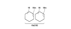
- FIG. 1 schematically shows a cross section of the aluminum nitride plate 10. Note that arrows 12 and 14 in the figure indicate the direction of the c-axis.
- the aluminum nitride plate 10 includes a surface layer 10a having a higher c-axis orientation degree (c-plane orientation degree) and a lower layer 10b having a c-axis orientation degree lower than that of the surface layer 10a.
- the c-plane orientation degree satisfies the above formulas 1 and 2.
- both the surface layer 10a and the lower layer 10b have a c-plane orientation degree of greater than 97% (the surface layer 10a is greater than 97.5%). Further, the twist angle of the surface layer 10a is smaller than the twist angle of the lower layer 10b and less than 2.5 °.
- a semiconductor (not shown) is grown on the surface of the surface layer 10a.
- the aluminum nitride plate 10 is produced using the plate-like aluminum nitride powder described above.
- the surface layer 10a and the lower layer 10b are made from substantially the same raw material (plate-like aluminum nitride powder), and the chemical compositions are substantially equal.
- both are substantially equal, and specifically, the difference between the two is less than 0.15% wt. Therefore, the characteristics of the surface layer 10a and the lower layer 10b are substantially equal.
- the broken line which divides the surface layer 10a and the lower layer 10b in FIG. 1 has shown that the plate-shaped aluminum nitride powder is grain-growth by sintering and comprises the surface layer 10a and the lower layer 10b, It does not necessarily mean a grain boundary.
- the raw material for each sheet (surface layer sheet, lower layer sheet) for producing the aluminum nitride plate 10 is in the form of a slurry, and plate-like aluminum nitride particles, calcium carbonate, yttria, and Ca—Al—O-based firing aids. It can be produced by preparing a mixed raw material in which an agent is mixed and adding a binder, a plasticizer, a dispersing agent and the like to the mixed raw material. If necessary, granular (spherical) aluminum nitride particles are added to the slurry raw material. As the plate-like aluminum nitride particles, those having a high aspect ratio (an aspect ratio of 3 or more) are used.
- FIG. 2 schematically shows the aluminum nitride crystals 16 and 18 constituting the surface layer 10a.
- c-planes of aluminum nitride crystals 16 and 18 appear.
- the crystal structure of the aluminum nitride crystal is a hexagonal system, and an m-plane appears on a plane orthogonal to the c-axis.
- FIG. 2 shows an m-plane 16 m of the aluminum nitride crystal 16 and an m-plane 18 m of the aluminum nitride crystal 18.
- the directions around the c-axis of each aluminum nitride crystal constituting the surface layer 10a are aligned, and the twist angle is less than 2.5 °.
- the twist angle is indicated by the X-ray rocking curve profile of the (102) plane of the aluminum nitride crystal of the surface layer 10a.
- FIG. 3 illustrates the peak (strongest peak) of the (102) plane of the aluminum nitride crystal. Whether or not the orientations of the aluminum nitride crystals in the surface layer 10a or the lower layer 10b are aligned around the c-axis can be determined by measuring each layer with an XRD apparatus and judging from the half-value width in the X-ray rocking curve profile of the (102) plane. it can. In the case of the aluminum nitride plate 10, the full width at half maximum b10 (corresponding to the twist angle w1) of the (102) plane of the surface layer 10a is less than 2.5 °.
- the half-value width b10 (corresponding to the twist angle w2) of the (102) plane of the lower layer 10b is larger than the twist angle of the surface layer 10a and satisfies the above formula 4. That is, the surface layer 10a is well aligned around the c axis of each aluminum nitride crystal, and the lower layer 10b is not aligned around the c axis of each aluminum nitride crystal as compared to the surface layer 10a.
- the surface layer 10a plays a role of growing a high-quality semiconductor
- the lower layer 10b plays a role of relaxing the force applied to the aluminum nitride plate 10 from the semiconductor element portion.
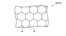
- FIG. 4 schematically shows the state of the surface layer 10a
- FIG. 5 schematically shows the state of the lower layer 10b.
- FIG. 4 when the orientations of the aluminum nitride crystals around the c-axis are aligned, the crystal orientations of the semiconductors grown on the aluminum nitride crystals are aligned, so that a high-quality (small defect) semiconductor can be obtained. it can.
- FIG. 5 if the directions around the c-axis of each aluminum nitride crystal are not aligned, for example, if the aluminum nitride crystal 18 rotates (twist) with respect to the aluminum nitride crystal 16, the crystal 16 , 18 is formed with a gap 20.
- the gap 20 relieves stress applied to the aluminum nitride plate 10 from the semiconductor (semiconductor element portion) during the manufacturing process of the semiconductor device or during use of the semiconductor device.
- the plate-like aluminum nitride particles were produced by heat-treating plate-like aluminum oxide in a heating furnace under nitrogen flow. Specifically, 100 g of plate-like aluminum oxide (Kinsei Matec Co., Ltd.), 50 g of carbon black (Mitsubishi Chemical Corporation), 1000 g of alumina cobblestone ( ⁇ 2 mm), IPA (isopropyl alcohol: manufactured by Tokuyama Co., Ltd., Toxo IPA) ) 350 mL was pulverized and mixed at 30 rpm for 240 minutes to obtain a mixture.
- the plate-like aluminum oxide having an average particle size (length in the surface direction) of 5 ⁇ m and 7 ⁇ m was used.
- Aluminum oxide having an average particle size of 5 ⁇ m had an average thickness (length in the thickness direction) of 0.07 ⁇ m and an aspect ratio of 70.
- Aluminum oxide having an average particle size of 7 ⁇ m had an average thickness (length in the thickness direction) of 0.1 ⁇ m and an aspect ratio of 70.
- the alumina cobblestone was removed from the obtained mixture, and the mixture was dried using a rotary evaporator. Thereafter, the remaining mixture (plate-like alumina, carbon mixture) was lightly crushed with a mortar (aggregated particles were separated by a relatively weak force).
- 100 g of the mixture is filled in a carbon crucible, placed in a heating furnace, heated to 1600 ° C. at a temperature rising rate of 200 ° C./hr under a flow of nitrogen gas of 3 L / min, and held at 1600 ° C. for 20 hours. did.
- the sample was naturally cooled, the sample was taken out from the crucible, and heat-treated (post-heated) at 650 ° C. for 10 hours in an oxidizing atmosphere using a muffle furnace to obtain plate-like aluminum nitride particles.
- the post heat treatment was performed to remove carbon remaining in the sample.
- the aluminum nitride particles after the heat treatment include single particles and aggregated particles. Therefore, the aluminum nitride particles after the heat treatment were crushed and classified to select single particles. Specifically, 100 g of aluminum nitride particles after heat treatment, 300 g of alumina cobblestone ( ⁇ 15 mm), and 60 mL of IPA (Tokuyama Co., Ltd., Tokuso IPA) were crushed at 30 rpm for 240 minutes. Thereafter, the alumina cobblestone was removed and dried using a rotary evaporator.
- the dried aluminum nitride particles were classified using a precision air sucker (manufactured by Nissin Engineering Co., Ltd., TC-15NSC).
- the classification point was set to the same size as the average particle diameter of the plate-like aluminum oxide described above.
- the fine particles after classification were used as the raw material for the aluminum nitride plate.
- a composite oxide of Ca and Al (Ca—Al—O-based auxiliary) was prepared as a sintering auxiliary. Specifically, calcium carbonate (manufactured by Shiraishi Calcium Co., Ltd., Silver-W) 56 g, ⁇ -alumina (manufactured by Daimei Chemical Co., Ltd., TM-300D) 19 g, alumina boulder ( ⁇ 15 mm) 1000 g, IPA (Tokuyama ( Co., Ltd., Toxo IPA) 125 mL was pulverized and mixed at 110 rpm for 120 minutes to obtain a mixture.
- raw materials for producing a tape molded body Three types are prepared by adjusting the ratio (mass ratio) of the plate-like aluminum nitride particles, the sintering aid, and commercially available aluminum nitride particles (manufactured by Tokuyama Corporation, F grade, average particle size 1.2 ⁇ m).
- Raw materials (tape raw materials 1 to 4) were prepared. Details of the tape raw materials 1 to 4 are shown in FIG.
- Three types of tape molded bodies were produced using tape raw materials 1 to 3. Specifically, 7.8 parts by mass of polyvinyl butyral (product number BM-2, manufactured by Sekisui Chemical Co., Ltd.) as a binder and di (2-ethylhexyl) phthalate (black gold) as a plasticizer with respect to 100 parts by mass of each tape raw material. 3.9 parts by mass of Kasei Chemical Co., Ltd., 2 parts by mass of sorbitan trioleate (manufactured by Kao, Leodol SP-O30) as a dispersant, and 2-ethylhexanol as a dispersion medium were added and mixed to prepare a raw material slurry.
- polyvinyl butyral product number BM-2, manufactured by Sekisui Chemical Co., Ltd.
- di (2-ethylhexyl) phthalate black gold
- sorbitan trioleate manufactured by Kao, Leodol SP-O30
- the amount of dispersion medium added was adjusted so that the slurry viscosity was 20000 cP.
- the raw material slurry was formed on the PET film by the doctor blade method so that the plate surfaces (c-plane) of the aluminum nitride particles were aligned along the surface of the tape molded body.
- the slurry thickness was adjusted so that the thickness after drying was 50 ⁇ m.
- each tape molded body was cut into a circle having a diameter of 20 mm, and each tape molded body was laminated to prepare five types of laminated molded bodies.
- a laminated molded body R1 in which 10 sheets of 1 were laminated and a laminated molded body R2 in which 10 tape molded bodies 2 were laminated were produced.
- Each laminated molded body was placed on an aluminum plate having a thickness of 10 mm, and then placed in a package, and the inside of the package was evacuated to form a vacuum package.
- Each vacuum package was hydrostatically pressed at a pressure of 100 kgf / cm 2 in 85 ° C. warm water to obtain a disk-shaped laminated molded body.
- each laminated molded body was first placed in a degreasing furnace and degreased at 600 ° C. for 10 hours.
- Each laminated compact after degreasing is fired in a nitrogen mold in a hot press at a firing temperature (maximum reached temperature) of 1850 ° C. for 5 hours under a surface pressure of 200 kgf / cm 2.
- the molded body was subjected to primary firing.
- the pressurizing direction at the time of hot pressing was set to the laminating direction of each laminated molded body (direction approximately orthogonal to the surface of the tape molded body). The pressurization was maintained until the temperature was lowered to room temperature.
- each laminated molded body after the primary calcination was performed.
- the surface of each laminated molded body after primary firing is ground, and the primary fired body prepared from S1, S2, and S3 is adjusted to ⁇ 20 mm and thickness 0.08 mm, and primary fired from R1 and R2.
- the body was adjusted to ⁇ 20 mm and thickness 0.23 mm.
- Each laminated molded body was filled in an aluminum nitride sheath, the inside of the heating furnace was in a nitrogen atmosphere, and baked at a firing temperature (maximum reached temperature) of 1900 ° C. for 75 hours, and each laminated molded body was subjected to secondary firing.
- each surface of the laminated compact after secondary firing and the front and back surfaces of a commercially available aluminum nitride single crystal are roughly polished, they are further fixed to a metal plate with a diameter of ⁇ 68 mm, and diamond abrasives having a particle size of 9 ⁇ m and 3 ⁇ m. It grind
- FIG. 7 shows combinations of materials (tape molded body, aluminum nitride single crystal) used in each aluminum nitride plate (samples 1 to 6).
- the used tapes 1 to 3 in FIG. 7 correspond to tape molded bodies obtained from the tape raw materials 1 to 3 in FIG. That is, the lower layer of sample 1 is a laminated molded body R1, the lower layer of sample 2 is a laminated molded body R2, the upper layer of sample 4 is a laminated molded body S3, the lower layer of sample 4 is a laminated molded body R1, and the upper layer of sample 5 is a laminated molded body. S1, the lower layer of sample 5 is a laminated molded body R1, the upper layer of sample 6 is a laminated molded body S2, and the lower layer of sample 6 is a secondary fired body manufactured using the laminated molded body R2.
- Sample 3 was not actually manufactured as a laminate, and the same aluminum nitride single crystal was evaluated as a surface layer or a lower layer.
- neither primary firing nor secondary firing was performed.
- the thicknesses of the surface layer and the lower layer can be arbitrarily adjusted by the number of tape molded bodies to be laminated, or after firing (after secondary firing) or after joining.
- samples 1 to 6 For the obtained samples (samples 1 to 6), the degree of orientation and the twist angle were measured, and the sample was evaluated for transparency, film formability, and workability. The evaluation results are shown in FIG. The measurement / evaluation method will be described below.
- the degree of orientation (f) was calculated by the Lotgering method. Specifically, the results P and P 0 obtained by the following formulas (3) and (4) were calculated by substituting them into the formula (2).
- P is a value obtained from XRD measurement of the obtained sample (aluminum nitride plate), and P 0 is a value calculated from standard aluminum nitride (JCPDS card No. 076-0567).
- JCPDS card No. 076-0567 As (hkl), (100), (002), (101), (102), (110), (103) were used.
- f ⁇ (P ⁇ P 0 ) / (1 ⁇ P 0 ) ⁇ ⁇ 100 (2)
- P 0 ⁇ I 0 (002) / ⁇ I 0 (hkl) (3)
- P ⁇ I (002) / ⁇ I (hkl) (4)
- the twist angle (half-value width in the X-ray rocking curve profile) was measured by irradiating the (102) plane of the surface layer and lower layer of each sample with X-rays. Specifically, using an XRD apparatus (D8-DISCOVER manufactured by Bruker-AXS), using a CuK ⁇ line, the voltage is 40 kV, the current is 40 mA, the collimator diameter is 0.5 mm, the anti-scattering slit is 3 mm, and the ⁇ step width is 0.01 °. Under the conditions, the XRD profile was measured at a counting time of 1 second. Based on the obtained XRC profile, the half width was calculated and used as the twist angle.
- FIG. 7 shows that for each sample, the c-layer orientation degree c1 of the surface layer, the c-plane orientation degree c2 of the lower layer, the twist angle w1 of the surface layer, and the twist angle w2 of the lower layer satisfy the following formulas (1) to (4). “O” is attached to the sample that is present, and “X” is attached to the sample that is not satisfied.
- Formula 1 c1> 97.5%
- Formula 2 c2> 97.0%
- Formula 3 w1 ⁇ 2.5 °
- Formula 4 w1 / w2 ⁇ 0.995
- Transparency was evaluated by measuring the linear transmittance at a wavelength of 450 nm using a spectrophotometer (manufactured by Perkin Elmer, Lambda 900) by cutting each sample into 10 mm length and 10 mm width.
- ⁇ is given to a sample having a linear transmittance of 40% or more
- X is given to a sample having a linear transmittance of less than 40%.
- the film formation surface (the surface of the Al 0.5 Ga 0.5 N layer) was observed with a scanning electron microscope (manufactured by JEOL Ltd., JSM-6390) at a magnification of 3000 times (more than 20 fields of view), cracks, pinholes
- the number of defects such as these was counted, and whether or not the number of defects was 100 / mm 2 or less was evaluated.
- “ ⁇ ” is given to a sample having a defect count of 100 / mm 2 or less
- “X” is given to a sample having a defect count of more than 100 / mm 2 .
- satisfying the formulas 1, 3, and 4 can grow a high-quality (small defect) semiconductor and obtain an aluminum nitride plate having high strength (high fracture toughness). . Further, it was confirmed that satisfying all of the formulas 1 to 4 enables growth of a high-quality semiconductor with high transparency and high strength (aluminum nitride plate can be obtained).
Landscapes
- Chemical & Material Sciences (AREA)
- Engineering & Computer Science (AREA)
- Organic Chemistry (AREA)
- Inorganic Chemistry (AREA)
- Materials Engineering (AREA)
- Manufacturing & Machinery (AREA)
- Ceramic Engineering (AREA)
- Crystallography & Structural Chemistry (AREA)
- Structural Engineering (AREA)
- Metallurgy (AREA)
- Physics & Mathematics (AREA)
- Computer Hardware Design (AREA)
- Condensed Matter Physics & Semiconductors (AREA)
- General Physics & Mathematics (AREA)
- Microelectronics & Electronic Packaging (AREA)
- Power Engineering (AREA)
- Chemical Kinetics & Catalysis (AREA)
- Thermal Sciences (AREA)
- Crystals, And After-Treatments Of Crystals (AREA)
- Chemical Vapour Deposition (AREA)
- Ceramic Products (AREA)
Abstract
Description
c1>97.5%・・・・・・(1)
c2>97.0%・・・・・・(2)
w1<2.5°・・・・・・・(3)
w1/w2<0.995・・・(4)
f={(P-P0)/(1-P0)}×100・・・(2)
P0=ΣI0(002)/ΣI0(hkl)・・・(3)
P=ΣI(002)/ΣI(hkl)・・・(4)
式1:c1>97.5%
式2:c2>97.0%
式3:w1<2.5°
式4:w1/w2<0.995
Claims (2)
- 窒化アルミニウム板であり、
表層を厚み方向からX線回折測定したときの(002)面の回折強度と(100)面の回折強度の合計に対する(002)面の回折強度の割合をc面配向度c1とし、
表層以外の部位を厚み方向からX線回折測定したときの(002)面の回折強度と(100)面の回折強度の合計に対する(002)面の回折強度の割合をc面配向度c2とし、
表層の(102)面のX線ロッキングカーブプロファイルにおける半値幅をw1とし、
表層以外の部位の(102)面のX線ロッキングカーブプロファイルにおける半値幅をw2としたときに、
以下の関係式(1)から(4)を満足している窒化アルミニウム板。
c1>97.5%・・・・・・(1)
c2>97.0%・・・・・・(2)
w1<2.5°・・・・・・・(3)
w1/w2<0.995・・・(4) - 表層の窒素含有量と表層以外の部位の窒素含有率の差が、重量比で、0.15%未満である、請求項1に記載の窒化アルミニウム板。
Priority Applications (5)
| Application Number | Priority Date | Filing Date | Title |
|---|---|---|---|
| CN201980005454.9A CN111868010B (zh) | 2018-03-27 | 2019-03-27 | 氮化铝板 |
| EP19775036.7A EP3778533A4 (en) | 2018-03-27 | 2019-03-27 | ALUMINUM NITRIDE FILM |
| JP2020509201A JP6872075B2 (ja) | 2018-03-27 | 2019-03-27 | 窒化アルミニウム板 |
| KR1020207030129A KR102519299B1 (ko) | 2018-03-27 | 2019-03-27 | 질화알루미늄판 |
| US17/030,960 US11383981B2 (en) | 2018-03-27 | 2020-09-24 | Aluminum nitride plate |
Applications Claiming Priority (2)
| Application Number | Priority Date | Filing Date | Title |
|---|---|---|---|
| JPPCT/JP2018/012542 | 2018-03-27 | ||
| JP2018012542 | 2018-03-27 |
Related Child Applications (1)
| Application Number | Title | Priority Date | Filing Date |
|---|---|---|---|
| US17/030,960 Continuation US11383981B2 (en) | 2018-03-27 | 2020-09-24 | Aluminum nitride plate |
Publications (1)
| Publication Number | Publication Date |
|---|---|
| WO2019189378A1 true WO2019189378A1 (ja) | 2019-10-03 |
Family
ID=68061827
Family Applications (2)
| Application Number | Title | Priority Date | Filing Date |
|---|---|---|---|
| PCT/JP2019/013227 WO2019189378A1 (ja) | 2018-03-27 | 2019-03-27 | 窒化アルミニウム板 |
| PCT/JP2019/013226 WO2019189377A1 (ja) | 2018-03-27 | 2019-03-27 | 窒化アルミニウム板 |
Family Applications After (1)
| Application Number | Title | Priority Date | Filing Date |
|---|---|---|---|
| PCT/JP2019/013226 WO2019189377A1 (ja) | 2018-03-27 | 2019-03-27 | 窒化アルミニウム板 |
Country Status (6)
| Country | Link |
|---|---|
| US (2) | US20210009418A1 (ja) |
| EP (1) | EP3778533A4 (ja) |
| JP (2) | JP6872074B2 (ja) |
| KR (1) | KR102519299B1 (ja) |
| CN (2) | CN111868010B (ja) |
| WO (2) | WO2019189378A1 (ja) |
Cited By (1)
| Publication number | Priority date | Publication date | Assignee | Title |
|---|---|---|---|---|
| WO2024053679A1 (ja) * | 2022-09-09 | 2024-03-14 | 京セラ株式会社 | セラミック構造体 |
Families Citing this family (3)
| Publication number | Priority date | Publication date | Assignee | Title |
|---|---|---|---|---|
| CN110402234B (zh) * | 2017-03-22 | 2022-10-14 | 日本碍子株式会社 | 氮化铝粒子 |
| US11318553B2 (en) * | 2019-01-04 | 2022-05-03 | Raytheon Technologies Corporation | Additive manufacturing of laminated superalloys |
| TW202134490A (zh) | 2020-03-13 | 2021-09-16 | 鴻創應用科技有限公司 | 氮化鋁晶圓片之製造方法及其氮化鋁晶圓片 |
Citations (8)
| Publication number | Priority date | Publication date | Assignee | Title |
|---|---|---|---|---|
| JPH08157265A (ja) * | 1994-12-05 | 1996-06-18 | Toshiba Corp | 窒化アルミニウム焼結体、複合基板およびその製造方法 |
| JPH1154603A (ja) * | 1997-08-06 | 1999-02-26 | Ngk Insulators Ltd | 半導体支持装置 |
| JP2006290729A (ja) * | 2003-06-30 | 2006-10-26 | Kenichiro Miyahara | 薄膜接合体 |
| JP2011020900A (ja) | 2009-07-16 | 2011-02-03 | Tokuyama Corp | 窒化アルミニウム単結晶層を有する積層体の製造方法、該製法で製造される積層体、該積層体を用いた窒化アルミニウム単結晶基板の製造方法、および、窒化アルミニウム単結晶基板 |
| WO2012008545A1 (ja) * | 2010-07-14 | 2012-01-19 | 住友金属鉱山株式会社 | 窒化アルミニウム結晶の製造方法 |
| JP2012031027A (ja) * | 2010-08-02 | 2012-02-16 | Tokyo Univ Of Agriculture & Technology | 単結晶窒化アルミニウムの製造方法 |
| JP2015133354A (ja) * | 2014-01-09 | 2015-07-23 | 日立金属株式会社 | 窒化物半導体エピタキシャルウェハ及び窒化物半導体デバイス |
| JP2016520992A (ja) * | 2013-03-14 | 2016-07-14 | ヘクサテック,インコーポレイテッド | 窒化アルミニウム単結晶基板を組込んだパワー半導体デバイス |
Family Cites Families (22)
| Publication number | Priority date | Publication date | Assignee | Title |
|---|---|---|---|---|
| US1755955A (en) * | 1927-11-25 | 1930-04-22 | Hagopian Serpoohie | Combined awning and screen |
| JP2916664B2 (ja) * | 1994-05-24 | 1999-07-05 | 株式会社ニッカトー | 配向性アルミナ質焼結体 |
| KR20010029852A (ko) * | 1999-06-30 | 2001-04-16 | 도다 다다히데 | Ⅲ족 질화물계 화합물 반도체 소자 및 그 제조방법 |
| US6602586B2 (en) * | 1999-08-05 | 2003-08-05 | Hayakawa Rubber Company Limited | Elastic blocks and process for producing the same |
| JPWO2004005216A1 (ja) | 2002-07-09 | 2005-11-04 | 宮原 健一郎 | 薄膜形成用基板、薄膜基板、光導波路、発光素子、及び発光素子搭載用基板 |
| EP1712662A4 (en) * | 2003-06-30 | 2009-12-02 | Kenichiro Miyahara | SUBSTRATE FOR THE MANUFACTURE OF THIN FILMS, SUBSTRATE FOR THIN FILMS AND LIGHT EMITTING ELEMENT |
| JP4615873B2 (ja) * | 2003-12-16 | 2011-01-19 | 株式会社トクヤマ | 窒化アルミニウム焼結体及びその製造方法 |
| JP4518209B1 (ja) * | 2009-09-07 | 2010-08-04 | 住友電気工業株式会社 | Iii族窒化物結晶基板、エピ層付iii族窒化物結晶基板、ならびに半導体デバイスおよびその製造方法 |
| JP4277826B2 (ja) * | 2005-06-23 | 2009-06-10 | 住友電気工業株式会社 | 窒化物結晶、窒化物結晶基板、エピ層付窒化物結晶基板、ならびに半導体デバイスおよびその製造方法 |
| CN101140969B (zh) * | 2006-09-08 | 2011-03-16 | 希特隆股份有限公司 | 化合物半导体器件及其制造方法 |
| TWI412069B (zh) * | 2010-12-27 | 2013-10-11 | Ind Tech Res Inst | 氮化物半導體基板及其製造方法 |
| CN102593080A (zh) * | 2011-01-11 | 2012-07-18 | 三菱综合材料株式会社 | 散热板、半导体装置和散热板的制造方法 |
| JP5757104B2 (ja) * | 2011-02-24 | 2015-07-29 | 住友電気工業株式会社 | マグネシウム合金材及びその製造方法 |
| WO2013021606A1 (ja) * | 2011-08-09 | 2013-02-14 | パナソニック株式会社 | 窒化物半導体層成長用構造、積層構造、窒化物系半導体素子および光源ならびにこれらの製造方法 |
| WO2014042054A1 (ja) * | 2012-09-11 | 2014-03-20 | 株式会社トクヤマ | 窒化アルミニウム基板およびiii族窒化物積層体 |
| CN104955769B (zh) * | 2013-02-08 | 2018-07-20 | 株式会社德山 | 氮化铝粉末 |
| CN106574399B (zh) * | 2014-08-01 | 2019-05-07 | 株式会社德山 | n型氮化铝单晶基板 |
| CN107001148B (zh) * | 2014-11-28 | 2020-03-13 | 日本碍子株式会社 | 氧化铝烧结体及光学元件用基底基板 |
| KR102382726B1 (ko) * | 2014-11-28 | 2022-04-06 | 엔지케이 인슐레이터 엘티디 | 투명 알루미나 소결체의 제법 |
| KR102557206B1 (ko) * | 2016-12-21 | 2023-07-18 | 엔지케이 인슐레이터 엘티디 | 배향 AlN 소결체 및 그 제법 |
| CN107516630B (zh) * | 2017-08-18 | 2019-11-01 | 广东省半导体产业技术研究院 | 一种AlN外延层及其制备方法 |
| JP6545862B1 (ja) * | 2018-04-20 | 2019-07-17 | 東芝エレベータ株式会社 | エレベータ機材の基準位置設定方法、エレベータ機材の設置方法、エレベータ機材の基準位置設定装置及び基準位置設定システム |
-
2019
- 2019-03-27 WO PCT/JP2019/013227 patent/WO2019189378A1/ja unknown
- 2019-03-27 WO PCT/JP2019/013226 patent/WO2019189377A1/ja active Application Filing
- 2019-03-27 EP EP19775036.7A patent/EP3778533A4/en active Pending
- 2019-03-27 CN CN201980005454.9A patent/CN111868010B/zh active Active
- 2019-03-27 JP JP2020509200A patent/JP6872074B2/ja active Active
- 2019-03-27 KR KR1020207030129A patent/KR102519299B1/ko active IP Right Grant
- 2019-03-27 JP JP2020509201A patent/JP6872075B2/ja active Active
- 2019-03-27 CN CN201980005455.3A patent/CN111868011B/zh active Active
-
2020
- 2020-09-24 US US17/030,895 patent/US20210009418A1/en active Pending
- 2020-09-24 US US17/030,960 patent/US11383981B2/en active Active
Patent Citations (8)
| Publication number | Priority date | Publication date | Assignee | Title |
|---|---|---|---|---|
| JPH08157265A (ja) * | 1994-12-05 | 1996-06-18 | Toshiba Corp | 窒化アルミニウム焼結体、複合基板およびその製造方法 |
| JPH1154603A (ja) * | 1997-08-06 | 1999-02-26 | Ngk Insulators Ltd | 半導体支持装置 |
| JP2006290729A (ja) * | 2003-06-30 | 2006-10-26 | Kenichiro Miyahara | 薄膜接合体 |
| JP2011020900A (ja) | 2009-07-16 | 2011-02-03 | Tokuyama Corp | 窒化アルミニウム単結晶層を有する積層体の製造方法、該製法で製造される積層体、該積層体を用いた窒化アルミニウム単結晶基板の製造方法、および、窒化アルミニウム単結晶基板 |
| WO2012008545A1 (ja) * | 2010-07-14 | 2012-01-19 | 住友金属鉱山株式会社 | 窒化アルミニウム結晶の製造方法 |
| JP2012031027A (ja) * | 2010-08-02 | 2012-02-16 | Tokyo Univ Of Agriculture & Technology | 単結晶窒化アルミニウムの製造方法 |
| JP2016520992A (ja) * | 2013-03-14 | 2016-07-14 | ヘクサテック,インコーポレイテッド | 窒化アルミニウム単結晶基板を組込んだパワー半導体デバイス |
| JP2015133354A (ja) * | 2014-01-09 | 2015-07-23 | 日立金属株式会社 | 窒化物半導体エピタキシャルウェハ及び窒化物半導体デバイス |
Non-Patent Citations (1)
| Title |
|---|
| See also references of EP3778533A4 |
Cited By (1)
| Publication number | Priority date | Publication date | Assignee | Title |
|---|---|---|---|---|
| WO2024053679A1 (ja) * | 2022-09-09 | 2024-03-14 | 京セラ株式会社 | セラミック構造体 |
Also Published As
| Publication number | Publication date |
|---|---|
| WO2019189377A1 (ja) | 2019-10-03 |
| CN111868011B (zh) | 2022-03-11 |
| JPWO2019189378A1 (ja) | 2020-10-22 |
| EP3778533A1 (en) | 2021-02-17 |
| US20210009418A1 (en) | 2021-01-14 |
| JPWO2019189377A1 (ja) | 2020-10-22 |
| KR102519299B1 (ko) | 2023-04-06 |
| US20210002138A1 (en) | 2021-01-07 |
| JP6872074B2 (ja) | 2021-05-19 |
| CN111868010B (zh) | 2023-04-28 |
| CN111868011A (zh) | 2020-10-30 |
| CN111868010A (zh) | 2020-10-30 |
| KR20200132977A (ko) | 2020-11-25 |
| JP6872075B2 (ja) | 2021-05-19 |
| US11383981B2 (en) | 2022-07-12 |
| EP3778533A4 (en) | 2021-12-15 |
Similar Documents
| Publication | Publication Date | Title |
|---|---|---|
| WO2019189378A1 (ja) | 窒化アルミニウム板 | |
| JP6681406B2 (ja) | エピタキシャル成長用配向アルミナ基板 | |
| WO2017057550A1 (ja) | アルミナ焼結体及び光学素子用下地基板 | |
| JPWO2020217564A1 (ja) | 半導体膜 | |
| JP6626500B2 (ja) | アルミナ焼結体及び光学素子用下地基板 | |
| TWI746750B (zh) | 配向AlN燒結體及其製法 | |
| JP7410009B2 (ja) | 半導体膜 | |
| KR102557205B1 (ko) | 투명 AlN 소결체 및 그 제법 | |
| JP6346718B1 (ja) | 窒化アルミニウム粒子 | |
| WO2019180937A1 (ja) | 窒化アルミニウム粒子 | |
| JP2005272203A (ja) | 膜形成用基板および半導体膜の形成方法 | |
| WO2024042591A1 (ja) | SiC基板及びSiC複合基板 | |
| JP7104266B1 (ja) | 希土類含有SiC基板及びSiC複合基板 | |
| WO2023062850A1 (ja) | 希土類含有SiC基板及びSiC複合基板 | |
| WO2022201986A1 (ja) | AlN単結晶基板 | |
| JP2018158885A (ja) | 窒化アルミニウム粒子 |
Legal Events
| Date | Code | Title | Description |
|---|---|---|---|
| 121 | Ep: the epo has been informed by wipo that ep was designated in this application |
Ref document number: 19775036 Country of ref document: EP Kind code of ref document: A1 |
|
| ENP | Entry into the national phase |
Ref document number: 2020509201 Country of ref document: JP Kind code of ref document: A |
|
| NENP | Non-entry into the national phase |
Ref country code: DE |
|
| ENP | Entry into the national phase |
Ref document number: 20207030129 Country of ref document: KR Kind code of ref document: A |
|
| ENP | Entry into the national phase |
Ref document number: 2019775036 Country of ref document: EP Effective date: 20201027 |