WO2019187635A1 - 撮像装置、制御方法、及びプログラム - Google Patents
撮像装置、制御方法、及びプログラム Download PDFInfo
- Publication number
- WO2019187635A1 WO2019187635A1 PCT/JP2019/003859 JP2019003859W WO2019187635A1 WO 2019187635 A1 WO2019187635 A1 WO 2019187635A1 JP 2019003859 W JP2019003859 W JP 2019003859W WO 2019187635 A1 WO2019187635 A1 WO 2019187635A1
- Authority
- WO
- WIPO (PCT)
- Prior art keywords
- unit
- temperature
- magnetism
- imaging
- image
- Prior art date
- Legal status (The legal status is an assumption and is not a legal conclusion. Google has not performed a legal analysis and makes no representation as to the accuracy of the status listed.)
- Ceased
Links
Images





Classifications
-
- G—PHYSICS
- G01—MEASURING; TESTING
- G01D—MEASURING NOT SPECIALLY ADAPTED FOR A SPECIFIC VARIABLE; ARRANGEMENTS FOR MEASURING TWO OR MORE VARIABLES NOT COVERED IN A SINGLE OTHER SUBCLASS; TARIFF METERING APPARATUS; MEASURING OR TESTING NOT OTHERWISE PROVIDED FOR
- G01D5/00—Mechanical means for transferring the output of a sensing member; Means for converting the output of a sensing member to another variable where the form or nature of the sensing member does not constrain the means for converting; Transducers not specially adapted for a specific variable
- G01D5/12—Mechanical means for transferring the output of a sensing member; Means for converting the output of a sensing member to another variable where the form or nature of the sensing member does not constrain the means for converting; Transducers not specially adapted for a specific variable using electric or magnetic means
- G01D5/14—Mechanical means for transferring the output of a sensing member; Means for converting the output of a sensing member to another variable where the form or nature of the sensing member does not constrain the means for converting; Transducers not specially adapted for a specific variable using electric or magnetic means influencing the magnitude of a current or voltage
- G01D5/142—Mechanical means for transferring the output of a sensing member; Means for converting the output of a sensing member to another variable where the form or nature of the sensing member does not constrain the means for converting; Transducers not specially adapted for a specific variable using electric or magnetic means influencing the magnitude of a current or voltage using Hall-effect devices
- G01D5/145—Mechanical means for transferring the output of a sensing member; Means for converting the output of a sensing member to another variable where the form or nature of the sensing member does not constrain the means for converting; Transducers not specially adapted for a specific variable using electric or magnetic means influencing the magnitude of a current or voltage using Hall-effect devices influenced by the relative movement between the Hall device and magnetic fields
-
- H—ELECTRICITY
- H04—ELECTRIC COMMUNICATION TECHNIQUE
- H04N—PICTORIAL COMMUNICATION, e.g. TELEVISION
- H04N23/00—Cameras or camera modules comprising electronic image sensors; Control thereof
- H04N23/60—Control of cameras or camera modules
- H04N23/68—Control of cameras or camera modules for stable pick-up of the scene, e.g. compensating for camera body vibrations
- H04N23/682—Vibration or motion blur correction
- H04N23/685—Vibration or motion blur correction performed by mechanical compensation
- H04N23/687—Vibration or motion blur correction performed by mechanical compensation by shifting the lens or sensor position
-
- G—PHYSICS
- G01—MEASURING; TESTING
- G01D—MEASURING NOT SPECIALLY ADAPTED FOR A SPECIFIC VARIABLE; ARRANGEMENTS FOR MEASURING TWO OR MORE VARIABLES NOT COVERED IN A SINGLE OTHER SUBCLASS; TARIFF METERING APPARATUS; MEASURING OR TESTING NOT OTHERWISE PROVIDED FOR
- G01D3/00—Indicating or recording apparatus with provision for the special purposes referred to in the subgroups
- G01D3/028—Indicating or recording apparatus with provision for the special purposes referred to in the subgroups mitigating undesired influences, e.g. temperature, pressure
- G01D3/036—Indicating or recording apparatus with provision for the special purposes referred to in the subgroups mitigating undesired influences, e.g. temperature, pressure on measuring arrangements themselves
- G01D3/0365—Indicating or recording apparatus with provision for the special purposes referred to in the subgroups mitigating undesired influences, e.g. temperature, pressure on measuring arrangements themselves the undesired influence being measured using a separate sensor, which produces an influence related signal
-
- G—PHYSICS
- G01—MEASURING; TESTING
- G01K—MEASURING TEMPERATURE; MEASURING QUANTITY OF HEAT; THERMALLY-SENSITIVE ELEMENTS NOT OTHERWISE PROVIDED FOR
- G01K1/00—Details of thermometers not specially adapted for particular types of thermometer
- G01K1/02—Means for indicating or recording specially adapted for thermometers
- G01K1/026—Means for indicating or recording specially adapted for thermometers arrangements for monitoring a plurality of temperatures, e.g. by multiplexing
-
- G—PHYSICS
- G02—OPTICS
- G02B—OPTICAL ELEMENTS, SYSTEMS OR APPARATUS
- G02B27/00—Optical systems or apparatus not provided for by any of the groups G02B1/00 - G02B26/00, G02B30/00
- G02B27/64—Imaging systems using optical elements for stabilisation of the lateral and angular position of the image
- G02B27/646—Imaging systems using optical elements for stabilisation of the lateral and angular position of the image compensating for small deviations, e.g. due to vibration or shake
-
- G—PHYSICS
- G03—PHOTOGRAPHY; CINEMATOGRAPHY; ANALOGOUS TECHNIQUES USING WAVES OTHER THAN OPTICAL WAVES; ELECTROGRAPHY; HOLOGRAPHY
- G03B—APPARATUS OR ARRANGEMENTS FOR TAKING PHOTOGRAPHS OR FOR PROJECTING OR VIEWING THEM; APPARATUS OR ARRANGEMENTS EMPLOYING ANALOGOUS TECHNIQUES USING WAVES OTHER THAN OPTICAL WAVES; ACCESSORIES THEREFOR
- G03B5/00—Adjustment of optical system relative to image or object surface other than for focusing
-
- H—ELECTRICITY
- H04—ELECTRIC COMMUNICATION TECHNIQUE
- H04N—PICTORIAL COMMUNICATION, e.g. TELEVISION
- H04N23/00—Cameras or camera modules comprising electronic image sensors; Control thereof
- H04N23/50—Constructional details
- H04N23/54—Mounting of pick-up tubes, electronic image sensors, deviation or focusing coils
-
- H—ELECTRICITY
- H04—ELECTRIC COMMUNICATION TECHNIQUE
- H04N—PICTORIAL COMMUNICATION, e.g. TELEVISION
- H04N23/00—Cameras or camera modules comprising electronic image sensors; Control thereof
- H04N23/50—Constructional details
- H04N23/55—Optical parts specially adapted for electronic image sensors; Mounting thereof
-
- H—ELECTRICITY
- H04—ELECTRIC COMMUNICATION TECHNIQUE
- H04N—PICTORIAL COMMUNICATION, e.g. TELEVISION
- H04N23/00—Cameras or camera modules comprising electronic image sensors; Control thereof
- H04N23/60—Control of cameras or camera modules
- H04N23/68—Control of cameras or camera modules for stable pick-up of the scene, e.g. compensating for camera body vibrations
- H04N23/681—Motion detection
- H04N23/6812—Motion detection based on additional sensors, e.g. acceleration sensors
Definitions
- the present disclosure relates to an imaging apparatus, a control method, and a program.
- Patent Documents 1 and 2 there has been disclosed a technique for correcting camera shake at the time of photographing in an imaging device that captures an optical image of a subject.
- the detection value of the detection unit provided for deriving the amount of camera shake is corrected according to the temperature inside the apparatus.
- JP 2013-88706 A Japanese Patent Laid-Open No. 2015-200787
- the detection value is simply corrected according to the temperature inside the apparatus in a configuration in which the image sensor is driven in a direction perpendicular to the optical axis in order to correct camera shake.
- the amount of camera shake cannot be derived properly.
- the accuracy of correcting the camera shake decreases.
- the present disclosure has been made in view of the above circumstances, and an object thereof is to provide an imaging device, a control method, and a program capable of accurately correcting camera shake when imaging is performed.
- an imaging apparatus includes a magnetism generation unit, a magnetism detection unit that detects magnetism generated by the magnetism generation unit, and one of the magnetism generation unit and the magnetism detection unit.
- An image sensor that outputs an image obtained by imaging an optical image that has passed through the imaging optical system is fixed, and a moving unit that moves the position of the image sensor in a direction perpendicular to the optical axis of the imaging optical system; Detects the temperature of the drive unit that moves the unit, the fixed unit that is fixed to the imaging device main body, the other of the magnetic generation unit or the magnetic detection unit, and the temperature of the magnetic generation unit, and outputs the detection result as the first temperature A first temperature detection unit that detects the temperature of the magnetic detection unit, and outputs the detection result as a second temperature; the detection result of the magnetic detection unit; the first temperature; and the second temperature. Based on the movement amount of the image sensor derived by And a control section for controlling to move the moving portion.
- the imaging device is the imaging device according to the first aspect, in which the control unit further determines the amount of movement based on the amount of deviation between the position of the magnetic generation unit and the position of the magnetic detection unit measured in advance. It may be derived.
- the imaging device is the imaging device according to the third aspect of the imaging device according to the first aspect or the second aspect, which is a temperature measured at a predetermined timing before imaging with the imaging element.
- a storage unit that stores the temperature and the fourth temperature of the magnetic detection unit may be provided, and the control unit may derive the movement amount of the moving unit based on the third temperature and the fourth temperature.
- control unit includes a movement amount and a shift amount of a predetermined center position of the captured image. Control of moving the moving unit by the driving unit may be performed based on the above.
- control unit determines the amount of deviation between the position of the magnetic generation unit measured in advance and the position of the magnetic detection unit. Based on this, a circuit unit that performs offset correction on the detection result of the magnetic detection unit may be provided.
- the magnetic detection unit may be a Hall element.
- the control method is to capture a magnetic generation unit, a magnetic detection unit that detects magnetism generated by the magnetic generation unit, and an optical image transmitted through one of the magnetic generation unit or the magnetic detection unit and an imaging optical system.
- An imaging device that outputs the captured image obtained in this manner is fixed, a moving unit that moves the position of the imaging device in a direction orthogonal to the optical axis of the imaging optical system, a driving unit that moves the moving unit, and a magnetic generation unit
- the other of the magnetic detection unit is fixed and fixed to the imaging apparatus body, the first temperature detection unit that detects the temperature of the magnetic generation unit, and outputs the detection result as the first temperature, and the magnetic detection unit And a second temperature detection unit that outputs the detection result as a second temperature, the control method of the imaging apparatus, wherein the detection result of the magnetic detection unit, the first temperature, and the second temperature Based on the movement amount of the image sensor derived based on the drive unit, Performs control to move more moving parts, including processing.
- the program according to the eighth aspect captures an optical image transmitted through an imaging optical system, a magnetism generation unit, a magnetism detection unit that detects magnetism generated by the magnetism generation unit, and either the magnetism generation unit or the magnetism detection unit.
- An imaging device that outputs the obtained captured image is fixed, a moving unit that moves the position of the imaging device in a direction orthogonal to the optical axis of the imaging optical system, a driving unit that moves the moving unit, and a magnetic generation unit or A fixing unit that is fixed to the imaging device body, the first temperature detecting unit that detects the temperature of the magnetism generating unit, and outputs the detection result as a first temperature; Based on the detection result of the magnetic detection unit, the first temperature, and the second temperature, the computer that controls the imaging apparatus including the second temperature detection unit that detects the temperature and outputs the detection result as the second temperature. Based on the derived movement amount of the image sensor, Performs control to move the moving portion by the movement unit to execute the process.
- camera shake can be accurately corrected when imaging is performed.
- the imaging device 10 is an interchangeable lens digital camera, and includes an imaging device body 12 and an imaging lens 14.
- the imaging lens 14 is attached to the imaging apparatus main body 12 in a replaceable manner.
- a still image imaging mode for recording a still image and a moving image imaging mode for recording a moving image are selectively set according to an instruction given from the user to the imaging device 10.
- the manual focus mode and the auto focus mode are selectively set according to an instruction given from the user to the image capturing apparatus 10.
- the autofocus is expressed as “AF (AutoFocus)”.
- the imaging condition is adjusted by pressing a release button (not shown) provided on the imaging apparatus main body 12 halfway, and then the main exposure is performed when the release button is fully pressed.
- a release button (not shown) provided on the imaging apparatus main body 12 halfway
- the AE (AutoExposure) function is activated and the exposure state is set, then the AF function is activated and focus control is performed, and the release button is fully depressed. Then, imaging is performed.
- the imaging device main body 12 includes a mount 13, and the imaging lens 14 includes a mount 15.
- the imaging lens 14 is replaceably attached to the imaging apparatus main body 12 when the mount 15 is coupled to the mount 13.
- the imaging lens 14 includes a lens unit 18, a diaphragm 19, and a control device 44.
- the diaphragm 19 is provided closer to the imaging device body 12 than the lens unit 18, adjusts the amount of subject light transmitted through the lens unit 18, and guides the subject light into the imaging device body 12.
- the control device 44 is electrically connected to the imaging device main body 12 via the mounts 13 and 15, and controls the entire imaging lens 14 in accordance with instructions from the imaging device main body 12.
- the imaging apparatus main body 12 includes an imaging element 22, a main body side main control unit 46, an imaging element driver 50, an image signal processing circuit 52, an image memory 54, an image processing unit 56, and a display control unit 58.
- the imaging apparatus main body 12 includes a reception I / F (Interface) 60, a reception device 62, a media I / F 64, and an external I / F 72. Further, the imaging apparatus main body 12 includes a drive unit 32, a hall element 34, a magnet 36, and a circuit unit 38.
- the main body side main control unit 46 is an example of a computer according to the technology of the present disclosure, and includes a CPU (Central Processing Unit) 74, a primary storage unit 76, and a secondary storage unit 78.
- the CPU 74 controls the entire imaging apparatus 10.
- the primary storage unit 76 is a volatile memory used as a work area or the like when executing various programs.
- An example of the primary storage unit 76 is RAM (Random Access Memory).
- the secondary storage unit 78 is a non-volatile memory in which various programs, various parameters, and the like including a camera shake correction control program are stored in advance.
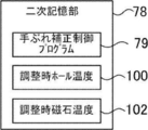
- An example of the secondary storage unit 78 is a flash memory. In the secondary storage unit 78 of the present embodiment, as shown in FIG.
- the above-mentioned camera shake correction control program 79 and the adjusted hall temperature 100 which is the temperature of the Hall element 34 measured in advance, which will be described in detail later.
- the magnet temperature during adjustment 102 which is the temperature of the magnet 36 measured in advance.
- the CPU 74 reads out the camera shake correction control program 79 from the secondary storage unit 78 and develops it in the primary storage unit 76, and executes the camera shake correction control process described in detail later according to the developed camera shake correction control program 79.
- the CPU 74 operates as the detection unit and the control unit of the present disclosure by executing the camera shake correction control program 79.
- the camera shake correction control program 79 of the present embodiment is an example of a program of the present disclosure.
- the CPU 74, the primary storage unit 76, and the secondary storage unit 78 are connected to the bus line 81.
- the image sensor driver 50 and the image signal processing circuit 52 are also connected to the bus line 81.
- the drive unit 32, the circuit unit 38, the image memory 54, the image processing unit 56, the display control unit 58, the reception I / F 60, the media I / F 64, and the external I / F 72 are also connected to the bus line 81.
- the image sensor driver 50 is connected to the image sensor 22.
- a CCD (Charge-Coupled Device) image sensor is used as the image sensor 22, but the technology of the present disclosure is not limited to this, for example, a CMOS (Complementary Metal-Oxide-Semiconductor) image sensor or the like. Other image sensors may be used.
- CMOS Complementary Metal-Oxide-Semiconductor
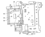
- the image sensor 22 of the present embodiment is fixed to a substrate 30.
- the substrate 30 drives the substrate 30 in a direction orthogonal to the optical axis L1 (FIG. 3A, arrow A direction and arrow B direction) according to the drive of the drive unit 32.
- the image sensor 22 fixed to the substrate 30 moves in a direction orthogonal to the optical axis L1.
- the substrate 30 is an example of the moving unit of the present disclosure.
- three VCMs Vehicle Coil Motor
- the driving unit 32 is not particularly limited as long as the substrate 30 can be driven in a direction orthogonal to the optical axis L1.
- camera shake is corrected by the drive unit 32 moving the substrate 30 in a direction orthogonal to the optical axis L1.
- the position of the substrate 30 is on the surface of the substrate 30 opposite to the surface on which the image sensor 22 is fixed (hereinafter referred to as “back surface”).
- Three Hall elements 34 used for detecting are fixed.
- the Hall element 34 of the present embodiment is driven by a drive circuit 90 (see FIG. 4).
- a temperature sensor 40 for detecting the temperature of the Hall element 34 is fixed to the back surface of the substrate 30 as shown in FIG. 3C.
- the temperature of the Hall element 34 may be detected by directly contacting the temperature of the Hall element 34 by bringing the temperature sensor 40 into contact with the Hall element 34 or by detecting the temperature in the vicinity of the Hall element 34.
- the temperature of the Hall element 34 may be indirectly detected by detecting using.
- the detection result of the temperature sensor 40 is output to the main body side main control unit 46 via the bus line 81.
- the detection result of the Hall element 34 is output to a circuit unit 38 to be described in detail later.
- the Hall element 34 of the present embodiment is an example of a magnetic detection unit of the present disclosure.
- the temperature sensor 40 of this embodiment is an example of the 2nd temperature detection part of this indication.
- a fixing portion 37 is provided on the back surface side of the substrate 30 at a position facing the substrate 30.
- three magnets 36 are fixed at positions corresponding to the three hall elements 34, respectively.
- the fixing unit 37 is fixed to the imaging device main body 12, and the position with respect to the imaging device main body 12 is fixed regardless of the movement of the substrate 30.
- a temperature sensor 42 for detecting the temperature of the magnet 36 is fixed to the fixing portion 37. The temperature of the magnet 36 may be detected by directly contacting the temperature of the magnet 36 by bringing the temperature sensor 42 into contact with the magnet 36 or by detecting the temperature near the magnet 36 using the temperature sensor 42.
- the temperature of the magnet 36 may be detected indirectly.
- the detection result of the temperature sensor 42 is output to the main body main controller 46 via the bus line 81.
- the magnet 36 of this embodiment is an example of the magnetic generation part of this indication.
- the temperature sensor 42 of the present embodiment is an example of the first temperature detection unit of the present disclosure.
- the Hall element 34 is fixed to the substrate 30, the magnet 36 may be fixed to the substrate 30. That is, it is only necessary that one of the magnet 36 or the Hall element 34 is fixed to the substrate 30. When the magnet 36 is fixed to the substrate 30, the Hall element 34 is fixed to the fixing portion 37. Further, although three Hall elements 34 and three magnets 36 are provided, the number is not limited to three.
- the image signal processing circuit 52 reads an image signal for one frame from the image sensor 22 for each pixel in accordance with the horizontal synchronization signal.
- the image signal processing circuit 52 performs various processes such as correlated double sampling processing, automatic gain adjustment, and A / D (Analog / Digital) conversion on the read image signal.
- the image signal processing circuit 52 converts the image signal digitized by performing various processes on the image signal at a specific frame rate (for example, several tens of frames / second) defined by the clock signal supplied from the CPU 74. Each frame is output to the image memory 54.
- the image memory 54 temporarily holds the image signal input from the image signal processing circuit 52.
- the image processing unit 56 acquires an image signal for each frame from the image memory 54 at a specific frame rate, and performs various processes such as gamma correction, luminance conversion, color difference conversion, and compression processing on the acquired image signal. Do. Further, the image processing unit 56 outputs an image signal obtained by performing various processes to the display control unit 58 for each frame at a specific frame rate. Further, the image processing unit 56 outputs an image signal obtained by performing various processes to the CPU 74 in response to a request from the CPU 74.
- the display control unit 58 is connected to the display 28 and the finder 67 of the touch panel display 29, and controls the display 28 and the finder 67 under the control of the CPU 74.
- the display control unit 58 outputs the image signal input from the image processing unit 56 to the display 28 and the finder 67 at a specific frame rate for each frame.
- the display 28 displays an image indicated by an image signal input at a specific frame rate from the display control unit 58 as a live view image.
- the display 28 also displays a still image that is a single frame image obtained by imaging in a single frame.
- a playback image and a menu screen are displayed on the display 28.
- the finder 67 is a so-called electronic view finder, and displays an image indicated by an image signal input at a specific frame rate from the display control unit 58 as a live view image, like the display 28.
- the receiving device 62 has a dial, a release button, a cross key, and the like, and receives various instructions from the user.
- the touch panel 61 and the reception device 62 of the touch panel display 29 are connected to the reception I / F 60 and output an instruction content signal indicating the content of the received instruction to the reception I / F 60.
- the reception I / F 60 outputs the input instruction content signal to the CPU 74.
- the CPU 74 executes a process according to the instruction content signal input from the reception I / F 60.
- a memory card 66 is detachably connected to the media I / F 64.
- the media I / F 64 records and reads an image file to and from the memory card 66 under the control of the CPU 74.
- the image file read from the memory card 66 by the media I / F 64 is decompressed by the image processing unit 56 under the control of the CPU 74 and displayed on the display 28 as a reproduced image.
- FIG. 4 shows an example of the circuit unit 38 of the present embodiment.
- the circuit unit 38 of the present embodiment is an offset circuit that performs offset correction on the detection result of the Hall element 34.
- the circuit unit 38 includes a differential amplifier 94, resistance elements R1 to R4, and an ADC (Analog-to-Digital Converter).
- the inverting input terminal of the differential amplifier 94 is connected to the Hall element 34 via the resistance element R1, and the Hall voltage is input from the Hall element 34. Further, the inverting input terminal of the differential amplifier 94 and the output are connected via a resistance element R3. On the other hand, the non-inverting input terminal of the differential amplifier 94 is connected to the Hall element 34 via the resistance element R ⁇ b> 2, and the Hall voltage is input from the Hall element 34. A non-inverting input terminal of the differential amplifier 94 is connected to a DAC (Digital-to-Analog-Converter) 92 via a resistance element R4, and an offset voltage Hoffset is input from the DAC 92.
- DAC Digital-to-Analog-Converter
- the differential amplifier 94 outputs a voltage Y obtained by amplifying the Hall voltage y of the Hall element 34 according to the amplification factor z to the ADC 96.
- the Hall voltage y is a voltage depending on the temperature of the Hall element 34 and the magnet 36.
- the input voltage Y of the ADC 96 is a Hall voltage after offset correction by the offset voltage Hoffset.
- the ADC 96 converts the input voltage Y from an analog value to a digital value, and outputs the converted value Yadc to the main body side main control unit 46.
- the main body side main control unit 46 sets a drive amount for driving the substrate 30 (the image sensor 22) to correct camera shake based on the conversion value Yadc input from the ADC 96 and the detection results of the temperature sensors 40 and 42.
- the substrate 30 is driven by the driving unit 32.
- the circuit unit 38 includes the ADC 96, but it goes without saying that the ADC 96 may be provided outside the circuit unit 38.
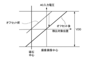
- the circuit unit 38 performs offset correction of the Hall voltage output from the Hall element 34. Therefore, in the imaging apparatus 10 of the present embodiment, offset correction is performed based on the temperature detected by each of the temperature sensors 40 and 42 at a predetermined timing for performing adjustment before shipping or the like, as shown in FIG. In addition, an offset value Hoffset for performing offset correction is acquired in a state where the output is “0” at the center of the captured image.
- the temperature T1 detected by the temperature sensor 40 is stored in advance in the secondary storage unit 78 as the adjusted hall temperature 100.
- the temperature T1 of the present embodiment is an example of a fourth temperature of the present disclosure.
- the temperature T2 detected by the temperature sensor 42 is stored in advance in the secondary storage unit 78 as the adjustment magnet temperature 102.
- the temperature T2 of the present embodiment is an example of a third temperature of the present disclosure.
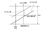
- the temperature of the Hall element 34 and the magnet 36 may be different from the temperature at the time of obtaining the offset value Hoffsetr.
- the temperature of the Hall element 34 provided in the vicinity of the image sensor 22 and the drive unit 32 rises according to the heat generation of the image sensor 22 or the drive unit 32, and is higher than the temperature of the magnet 36 fixed to the fixed unit 37.
- Each of the magnetic flux sensitivity of the Hall element 34 and the residual magnetic flux density of the magnet 36 changes according to the temperature. Specifically, each of the magnetic flux sensitivity of the Hall element 34 and the residual magnetic flux density of the magnet 36 decreases as the temperature increases. When the temperature of the Hall element 34 is higher than that of the magnet 36, the magnetic flux sensitivity of the Hall element 34 decreases more rapidly than the decrease in the residual density of the magnet 36.
- the main body side main control unit 46 of the imaging apparatus 10 detects the detection result (Hall voltage) of the Hall element 34. And the actual temperature of the Hall element 34 (the detection result of the temperature sensor 40) when photographing, and the temperature of the magnet 36 (the detection result of the temperature sensor 42), the amount of movement of the substrate 30 that has moved due to camera shake. To correct camera shake.
- the camera shake correction control process and control method performed by the main body side main control unit 46 will be described with reference to the drawings.
- the CPU 74 of the main body side main control unit 46 of the present embodiment executes the camera shake correction control program 79
- the main body side main control unit 46 functions as the control unit of the present disclosure, and the image stabilization shown in FIG. Control processing is executed.
- the camera shake correction control process illustrated in FIG. 7 is executed.
- the main body side main control unit 46 acquires the conversion value Yadc from the ADC 96.
- the main body side main controller 46 obtains the current temperature t1 of the magnet 36 as a detection result from the temperature sensor 42, and obtains the current temperature t2 of the hall element 34 as a detection result from the temperature sensor 40. get.
- the detection result of the temperature sensor 40 is an example of the second temperature of the present disclosure
- the detection result of the temperature sensor 42 is an example of the first temperature of the present disclosure.
- the main body side main control unit 46 derives a deviation amount with respect to the center of the captured image.
- the main body side main control unit 46 acquires the adjusted hall temperature 100 (temperature T1) and the adjusted magnet temperature 102 (temperature T2) from the secondary storage unit 78.
- the current hall voltage y is expressed by the following equation (2) based on the overall reduction rate and the hall output voltage x when the above-described adjustment is performed.
- the input voltage Y is expressed by the following equation (3).
- Z in the following equation (3) represents the amplification factor of the differential amplifier 94.
- the input voltage Y is derived from the above equations (4) and (5) by the following equation (7).
- Y Z ⁇ (1 + a) ⁇ x + VDD ⁇ 2-Z ⁇ L (7)
- the conversion value Yadc is obtained by the following equation (8).
- FS in the following equation (8) is the maximum value of the AD value determined by the number of bits of the ADC 96.
- Yadc Y ⁇ FS ⁇ VDD (8)
- the conversion value Yadc is expressed by the following formula (9). Therefore, the Hall voltage x is obtained by the following equation (10).
- Yadc [Z ⁇ (1 + a) ⁇ x + VDD ⁇ 2-Z ⁇ L] ⁇ FS ⁇ VDD (9)
- x [Yadc ⁇ (Z ⁇ FS ⁇ VDD) ⁇ VDD ⁇ (2 ⁇ Z) + L] ⁇ (1 + a) (10)
- the main body side main control unit 46 derives the relative distance to the center of the captured image, which corresponds to the value of x ⁇ L. Therefore, the main body side main control unit 46 derives the value of x ⁇ L by the following equation (11).
- the main body side main control unit 46 drives the substrate 30 by the drive unit 32 based on the value of x ⁇ L derived by the equation (11) in the above step S104, whereby the image pickup device 22 is driven. , The camera shake correction is performed, and then the camera shake correction control process is terminated.
- the imaging apparatus 10 of the present embodiment includes the magnet 36, the Hall element 34 that detects the magnetism generated by the magnet 36, and the optical image transmitted through one of the magnet 36 or the Hall element 34 and the imaging optical system.
- the image pickup device 22 that outputs the picked-up image obtained by picking up the image is fixed, the substrate 30 that moves the position of the image pickup device 22 in the direction orthogonal to the direction of the optical axis L1 of the image pickup optical system, and the substrate 30 is driven.
- Temperature sensor that detects the temperature of the driving unit 32, the fixing unit 37 to which the other of the magnet 36 or the Hall element 34 is fixed and is fixed to the imaging apparatus body 12, and the temperature of the magnet 36, and outputs the detection result as the temperature t1.
- a temperature sensor 40 that detects the temperature of the Hall element 34, and outputs the detection result as a temperature t2, and an imaging derived based on the detection result of the Hall element 34, the temperature t1, and the temperature t2.
- a body-side main control unit 46 for controlling to drive the substrate 30, a by driving unit 32.
- the camera shake correction is controlled based on the current temperatures t1 and t2 at which camera shake correction is performed, the temperatures T1 and T2 at the time of adjustment are different from the temperatures t1 and t2. Even in such a case, camera shake can be accurately corrected.
- a magnetic detection part is not limited to Hall element 34, What is necessary is just a magnetic sensor which can detect magnetism, for example, A magnetoresistive effect element, a magneto-impedance element, etc. may be sufficient.
- the present invention is not limited to this embodiment, and the main body side main control unit 46 and the like may perform the offset correction by software control. Good.
- various processors other than the CPU may execute various processes executed by the CPU executing software (programs) in each of the above embodiments.
- a processor in this case, in order to execute specific processing such as PLD (Programmable Logic Device) and ASIC (Application Specific Integrated Circuit) whose circuit configuration can be changed after manufacturing FPGA (Field-Programmable Gate Array) or the like
- a dedicated electric circuit which is a processor having a circuit configuration designed exclusively, is exemplified.
- the above-described various processes may be executed by one of these various processors, or a combination of two or more processors of the same type or different types (for example, a combination of a plurality of FPGAs and CPUs and FPGAs). Etc.).
- the hardware structure of these various processors is more specifically an electric circuit in which circuit elements such as semiconductor elements are combined.
- the image stabilization control program 79 includes a CD-ROM (Compact Disk Read Only Memory) and a DVD-ROM. (Digital Versatile Disk Read Only Memory) and USB (Universal Serial Bus) You may provide with the form recorded on recording media, such as memory. Further, the camera shake correction control program 79 may be downloaded from an external device via a network.
- CD-ROM Compact Disk Read Only Memory
- DVD-ROM Digital Versatile Disk Read Only Memory
- USB Universal Serial Bus
- a magnetic generator A magnetic detection device for detecting magnetism generated by the magnetic generation device; One of the magnetism generation device or the magnetism detection device and an image sensor that outputs a captured image obtained by capturing an optical image transmitted through the image capture optical system are fixed, and the position of the image sensor is determined by the position of the image capture optical system.
- the other of the magnetism generating device or the magnetism detecting device is fixed, and a fixing plate fixed to the imaging device main body,
- a first temperature detection sensor that detects a temperature of the magnetic generator and outputs a detection result as a first temperature;
- a second temperature detection sensor that detects a temperature of the magnetic detection device and outputs a detection result as a second temperature;
- a processor that performs control to move the substrate by the driving device based on a detection result of the magnetic detection device, a moving amount of the imaging element derived based on the first temperature and the second temperature;
- An imaging apparatus comprising:
- Imaging device 12 Imaging device main body 13, 15 Mount 14 Imaging lens 16 Focus ring 18 Lens unit 19 Aperture 22 Imaging element 28 Display 29 Touch panel display 30 Substrate 32 Drive part 34 Hall element 36 Magnet 37 Fixing part 38 Circuit part 40, 42 Temperature Sensor 44 Controller 46 Main body side main controller 50 Image sensor driver 52 Image signal processing circuit 54 Image memory 56 Image processor 58 Display controller 60 Reception I / F 61 Touch panel 62 Reception device 64 Media I / F 66 Memory card 67 Finder 72 External I / F 74 CPU 76 Primary storage unit 78 Secondary storage unit 79 Camera shake correction control program 81 Bus line 90 Drive circuit 92 DAC 94 Differential Amplifier 96 ADC 100 Hall temperature during adjustment 102 Magnet temperature during adjustment A and B Arrows R1 to R4 Resistance element
Landscapes
- Physics & Mathematics (AREA)
- General Physics & Mathematics (AREA)
- Engineering & Computer Science (AREA)
- Multimedia (AREA)
- Signal Processing (AREA)
- Optics & Photonics (AREA)
- Adjustment Of Camera Lenses (AREA)
- Studio Devices (AREA)
Abstract
撮像を行う場合に、手ぶれを精度よく補正することができる撮像装置、制御方法、及びプログラムを提供する。撮像装置(10)は、磁石(36)と、磁石(36)が発生した磁気を検出するホール素子(34)と、磁石(36)またはホール素子(34)の一方と撮像光学系を透過した光学像を撮像して得られた撮像画像を出力する撮像素子(22)とが固定され撮像素子(22)の位置を光軸(L1)と直交する方向に移動する基板(30)と、基板(30)を駆動する駆動部(32)と、磁石(36)またはホール素子(34)の他方が固定され撮像装置本体(12)に固定される固定部(37)と、ホール素子(34)の検出結果、磁石(36)の温度t1及びホール素子(34)の温度t2に基づいて導出した撮像素子(22)の移動量に基づいて基板(30)を駆動する制御を行う本体側主制御部(46)とを備える。
Description
本開示は、撮像装置、制御方法、及びプログラムに関する。
従来、被写体の光学像を撮像する撮像装置において、撮影の際の手ぶれを補正する技術が開示されている。(特許文献1及び2参照)。
特許文献1及び2に開示の技術では、手ぶれ量を導出するために設けられた検出部の検出値に対して、装置内部の温度に応じた補正を行っている。
しかしながら、上記特許文献1及び2に記載の技術では、手ぶれを補正するために、撮像素子を光軸と垂直な方向に駆動する構成において、上記検出値を単に、装置内部の温度に応じて補正するだけでは、手ぶれ量を適切に導出できない場合があった。この場合、導出される手ぶれ量が不適切な値となるため、手ぶれを補正する精度が低下する。
本開示は、以上の事情を鑑みて成されたものであり、撮像を行う場合に、手ぶれを精度よく補正することができる、撮像装置、制御方法、及びプログラムを提供することを目的とする。
上記目的を達成するために、本開示の第1の態様の撮像装置は、磁気発生部と、磁気発生部が発生した磁気を検出する磁気検出部と、磁気発生部または磁気検出部の一方と撮像光学系を透過した光学像を撮像して得られた撮像画像を出力する撮像素子とが固定され、撮像素子の位置を撮像光学系の光軸と直交する方向に移動する移動部と、移動部を移動する駆動部と、磁気発生部または磁気検出部の他方が固定され、かつ撮像装置本体に固定される固定部と、磁気発生部の温度を検出し、検出結果を第1温度として出力する第1温度検出部と、磁気検出部の温度を検出し、検出結果を第2温度として出力する第2温度検出部と、磁気検出部の検出結果、第1温度、及び第2温度に基づいて導出した撮像素子の移動量に基づいて、駆動部により移動部を移動する制御を行う制御部と、を備える。
第2の態様の撮像装置は、第1の態様の撮像装置において、制御部は、さらに、予め測定された磁気発生部の位置と、磁気検出部の位置とのずれ量に基づいて移動量を導出してもよい。
第3の態様の撮像装置は、第1の態様または第2の態様の撮像装置において、撮像素子により撮像を行う前の予め定められたタイミングで各々測定された温度である磁気発生部の第3温度、及び磁気検出部の第4温度を記憶する記憶部を備え、制御部は、さらに第3温度及び第4温度に基づいて、移動部の移動量を導出してもよい。
第4の態様の撮像装置は、第1の態様から第3の態様のいずれか1態様の撮像装置において、制御部は、移動量と、予め定められた撮像画像の中心の位置のずれ量とに基づいて駆動部により移動部を移動する制御を行ってもよい。
第5の態様の撮像装置は、第1の態様から第4の態様のいずれか1態様において、制御部は、予め測定された磁気発生部の位置と、磁気検出部の位置とのずれ量に基づいて、磁気検出部の検出結果をオフセット補正する回路部を備えてもよい。
第6の態様の撮像装置は、第1の態様から第5の態様のいずれか1態様において、磁気検出部は、ホール素子であってもよい。
第7の態様の制御方法は、磁気発生部と、磁気発生部が発生した磁気を検出する磁気検出部と、磁気発生部または磁気検出部の一方と撮像光学系を透過した光学像を撮像して得られた撮像画像を出力する撮像素子とが固定され、撮像素子の位置を撮像光学系の光軸と直交する方向に移動する移動部と、移動部を移動する駆動部と、磁気発生部または磁気検出部の他方が固定され、かつ撮像装置本体に固定される固定部と、磁気発生部の温度を検出し、検出結果を第1温度として出力する第1温度検出部と、磁気検出部の温度を検出し、検出結果を第2温度として出力する第2温度検出部と、を備えた撮像装置の制御方法であって、 磁気検出部の検出結果、第1温度、及び第2温度に基づいて導出した撮像素子の移動量に基づいて、駆動部により移動部を移動する制御を行う、処理を含む。
第8の態様のプログラムは、磁気発生部と、磁気発生部が発生した磁気を検出する磁気検出部と、磁気発生部または磁気検出部の一方と撮像光学系を透過した光学像を撮像して得られた撮像画像を出力する撮像素子とが固定され、撮像素子の位置を撮像光学系の光軸と直交する方向に移動する移動部と、移動部を移動する駆動部と、磁気発生部または磁気検出部の他方が固定され、かつ撮像装置本体に固定される固定部と、磁気発生部の温度を検出し、検出結果を第1温度として出力する第1温度検出部と、磁気検出部の温度を検出し、検出結果を第2温度として出力する第2温度検出部と、を備えた撮像装置を制御するコンピュータに、磁気検出部の検出結果、第1温度、及び第2温度に基づいて導出した撮像素子の移動量に基づいて、駆動部により移動部を移動する制御を行う、処理を実行させる。
本開示によれば、撮像を行う場合に、手ぶれを精度よく補正することができる。
以下、図面を参照して、本開示の技術を実施するための形態例を詳細に説明する。
まず、本実施形態の撮像装置10の構成を説明する。図1に示すように、撮像装置10は、レンズ交換式のデジタルカメラであり、撮像装置本体12及び撮像レンズ14を含む。撮像レンズ14は、撮像装置本体12に対して交換可能に装着される。
撮像装置10では、ユーザから撮像装置10に対して与えられた指示に応じて、静止画像を記録する静止画撮像モードと、動画像を記録する動画撮像モードとが選択的に設定される。また、静止画撮像モードでは、ユーザから撮像装置10に対して与えられた指示に応じて、マニュアルフォーカスモードとオートフォーカスモードとが選択的に設定される。なお、以下では、オートフォーカスを「AF(AutoFocus)」と表記する。
AFモードでは、撮像装置本体12に設けられたレリーズボタン(図示省略)を半押し状態にすることにより撮像条件の調整が行われ、その後、引き続き全押し状態にすると本露光が行われる。つまり、レリーズボタンを半押し状態にすることによりAE(AutoExposure:自動露出)機能が働いて露出状態が設定された後、AF機能が働いて合焦制御が行われ、レリーズボタンを全押し状態にすると撮像が行われる。
撮像装置本体12はマウント13を備えており、撮像レンズ14は、マウント15を備えている。撮像レンズ14は、マウント13にマウント15が結合されることにより撮像装置本体12に交換可能に装着される。撮像レンズ14は、レンズユニット18、絞り19、及び制御装置44を含む。絞り19は、レンズユニット18よりも撮像装置本体12側に設けられており、レンズユニット18を透過した被写体光の光量を調節し、被写体光を撮像装置本体12内に導く。制御装置44は、マウント13及び15を介して撮像装置本体12に電気的に接続されており、撮像装置本体12からの指示に従って撮像レンズ14の全体を制御する。
撮像装置本体12は、撮像素子22、本体側主制御部46、撮像素子ドライバ50、画像信号処理回路52、画像メモリ54、画像処理部56、及び表示制御部58を含む。また、撮像装置本体12は、受付I/F(Interface)60、受付デバイス62、メディアI/F64、及び外部I/F72を含む。さらに、撮像装置本体12は、駆動部32、ホール素子34、磁石36、及び回路部38を含む。
本体側主制御部46は、本開示の技術のコンピュータの一例であり、CPU(Central Processing Unit)74、一次記憶部76、及び二次記憶部78を備えている。CPU74は、撮像装置10の全体を制御する。一次記憶部76は、各種プログラムの実行時のワークエリア等として用いられる揮発性のメモリである。一次記憶部76の一例としては、RAM(Random Access Memory)が挙げられる。二次記憶部78は、手ぶれ補正制御プログラムを含む、各種プログラム及び各種パラメータ等を予め記憶した不揮発性のメモリである。二次記憶部78の一例としては、フラッシュメモリが挙げられる。なお、本実施形態の二次記憶部78には、図2に示すように、上記の手ぶれ補正制御プログラム79と、詳細を後述する予め測定されたホール素子34の温度である調整時ホール温度100、及び予め測定された磁石36の温度である調整時磁石温度102とが予め記憶されている。
CPU74は、二次記憶部78から手ぶれ補正制御プログラム79を読み出して一次記憶部76に展開し、展開した手ぶれ補正制御プログラム79に従って詳細を後述する手ぶれ補正制御処理を実行する。換言すると、CPU74は、手ぶれ補正制御プログラム79を実行することで本開示の検出部及び制御部として動作する。本実施形態の手ぶれ補正制御プログラム79が、本開示のプログラムの一例である。
CPU74、一次記憶部76、及び二次記憶部78は、バスライン81に接続されている。また、撮像素子ドライバ50、及び画像信号処理回路52も、バスライン81に接続されている。また、駆動部32、回路部38、画像メモリ54、画像処理部56、表示制御部58、受付I/F60、メディアI/F64、及び外部I/F72も、バスライン81に接続されている。
撮像素子ドライバ50は、撮像素子22に接続されている。本実施形態では、撮像素子22として、CCD(Charge Coupled Device)イメージセンサを用いているが、本開示の技術はこれに限定されず、例えば、CMOS(Complementary Metal-Oxide-Semiconductor)イメージセンサ等の他のイメージセンサを用いてもよい。
図1及び3A~3Cに示すように、本実施形態の撮像素子22は、基板30に固定されている。基板30は、駆動部32の駆動に応じて、基板30を光軸L1と直交する方向(図3A、矢印A方向及び矢印B方向)に駆動させる。基板30が駆動することにより、基板30に固定されている撮像素子22が光軸L1と直交する方向に移動する。なお、基板30が、本開示の移動部の一例である。駆動部32は本実施形態では一例として、3つのVCM(Voice Coil Motor)を適用しているが、特に限定されず、基板30を光軸L1と直交する方向に駆動可能であればよい。
本実施形態の撮像装置10では、駆動部32が基板30を、光軸L1と直交する方向に移動させることにより、手ぶれの補正が行われる。
また、図1及び図3Cに示すように、基板30の、撮像素子22が固定されている面の反対側の面(以下、「裏面」という)には、基板30(撮像素子22)の位置を検出するために用いられるホール素子34が3つ固定されている。本実施形態のホール素子34は駆動回路90(図4参照)によって駆動する。
さらに、基板30の裏面には、図3Cに示すように、ホール素子34の温度を検出するための温度センサ40が固定されている。なお、ホール素子34の温度の検出は、温度センサ40をホール素子34に接触等させて、ホール素子34の温度を直接、検出してもよいし、ホール素子34の近傍の温度を温度センサ40を用いて検出することにより、ホール素子34の温度を間接的に検出してもよい。温度センサ40の検出結果は、バスライン81を介して本体側主制御部46に出力される。ホール素子34の検出結果は、詳細を後述する回路部38に出力される。なお、本実施形態のホール素子34が、本開示の磁気検出部の一例である。また、本実施形態の温度センサ40が、本開示の第2温度検出部の一例である。
また、図1、図3A~3Cに示すように、基板30の裏面側に、基板30と対向する位置に、固定部37が設けられている。固定部37は、3つのホール素子34の各々と対応する位置に、3つの磁石36が固定されている。また、固定部37は、撮像装置本体12に固定されており、基板30の移動にかかわらず、撮像装置本体12に対する位置が固定されている。さらに、固定部37には、図3Bに示すように、磁石36の温度を検出するための温度センサ42が固定されている。なお、磁石36の温度の検出は、温度センサ42を磁石36に接触等させて、磁石36の温度を直接、検出してもよいし、磁石36の近傍の温度を温度センサ42を用いて検出することにより、磁石36の温度を間接的に検出してもよい。温度センサ42の検出結果は、バスライン81を介して本体側主制御部46に出力される。なお、本実施形態の磁石36は、本開示の磁気発生部の一例である。また、本実施形態の温度センサ42が、本開示の第1温度検出部の一例である。
なお、ホール素子34が基板30に固定されているとしたが、磁石36が基板30に固定されていてもよい。すなわち、磁石36またはホール素子34の一方が基板30に固定されていればよい。磁石36が基板30に固定される場合、ホール素子34が固定部37に固定される。また、ホール素子34及び磁石36は、それぞれ3つ設けられるとしたが、3つに限らない。
なお、ホール素子34が基板30に固定されているとしたが、磁石36が基板30に固定されていてもよい。すなわち、磁石36またはホール素子34の一方が基板30に固定されていればよい。磁石36が基板30に固定される場合、ホール素子34が固定部37に固定される。また、ホール素子34及び磁石36は、それぞれ3つ設けられるとしたが、3つに限らない。
画像信号処理回路52は、水平同期信号に応じて撮像素子22から1フレーム分の画像信号を画素毎に読み出す。画像信号処理回路52は、読み出した画像信号に対して、相関二重サンプリング処理、自動利得調整、及びA/D(Analog/Digital)変換等の各種処理を行う。画像信号処理回路52は、画像信号に対して各種処理を行うことによりデジタル化した画像信号を、CPU74から供給されるクロック信号で規定される特定のフレームレート(例えば、数十フレーム/秒)で1フレーム毎に画像メモリ54に出力する。
画像メモリ54は、画像信号処理回路52から入力された画像信号を一時的に保持する。
画像処理部56は、画像メモリ54から特定のフレームレートで1フレーム毎に画像信号を取得し、取得した画像信号に対して、ガンマ補正、輝度変換、色差変換、及び圧縮処理等の各種処理を行う。また、画像処理部56は、各種処理を行って得た画像信号を特定のフレームレートで1フレーム毎に表示制御部58に出力する。更に、画像処理部56は、各種処理を行って得た画像信号を、CPU74の要求に応じて、CPU74に出力する。
表示制御部58は、タッチパネルディスプレイ29のディスプレイ28、及びファインダ67に接続されており、CPU74の制御下で、ディスプレイ28、及びファインダ67を制御する。また、表示制御部58は、画像処理部56から入力された画像信号を1フレーム毎に特定のフレームレートでディスプレイ28、及びファインダ67に出力する。
ディスプレイ28は、表示制御部58から特定のフレームレートで入力された画像信号により示される画像をライブビュー画像として表示する。また、ディスプレイ28は、単一フレームで撮像されて得られた単一フレーム画像である静止画像も表示する。なお、ディスプレイ28には、ライブビュー画像の他に、再生画像及びメニュー画面等が表示される。ファインダ67は、いわゆる電子ビューファインダであり、ディスプレイ28と同様に、表示制御部58から特定のフレームレートで入力された画像信号により示される画像をライブビュー画像として表示する。
受付デバイス62は、ダイヤル、レリーズボタン、及び十字キー等を有しており、ユーザによる各種指示を受け付ける。
タッチパネルディスプレイ29のタッチパネル61及び受付デバイス62は、受付I/F60に接続されており、受け付けた指示の内容を示す指示内容信号を受付I/F60に出力する。受付I/F60は、入力された指示内容信号をCPU74に出力する。CPU74は、受付I/F60から入力された指示内容信号に応じた処理を実行する。
メディアI/F64には、メモリカード66が着脱可能に接続されている。メディアI/F64は、CPU74の制御下で、メモリカード66に対する画像ファイルの記録及び読み出しを行う。メディアI/F64によってメモリカード66から読み出された画像ファイルは、CPU74の制御下で、画像処理部56によって伸長処理が施されてディスプレイ28に再生画像として表示される。
次に、本実施形態の撮像装置10における、手ぶれ量、換言すると基板30の移動量を導出する構成について説明する。図4には、本実施形態の回路部38の一例を示す。本実施形態の回路部38は、ホール素子34の検出結果に対して、オフセット補正を行うオフセット回路である。回路部38は、差動アンプ94と、抵抗素子R1~R4と、ADC(Analog to Digital Converter)と、を備える。
差動アンプ94の反転入力端子は、抵抗素子R1を介してホール素子34に接続されており、ホール素子34からホール電圧が入力される。また、差動アンプ94の反転入力端子と、出力とは、抵抗素子R3を介して接続されている。一方、差動アンプ94の非反転入力端子は、抵抗素子R2を介してホール素子34に接続されており、ホール素子34からホール電圧が入力される。また、差動アンプ94の非反転入力端子は、抵抗素子R4を介してDAC(Digital to Analog Converter)92が接続されており、DAC92からオフセット電圧Hoffsetが入力される。
差動アンプ94は、ホール素子34のホール電圧yを増幅率zに応じて増幅した電圧YをADC96に出力する。ここでホール電圧yは、ホール素子34及び磁石36の温度に依存した電圧となっている。ADC96の入力電圧Yは、オフセット電圧Hoffsetによりオフセット補正後のホール電圧である。
ADC96は、入力電圧Yをアナログ値からデジタル値に変換し、変換値Yadcを本体側主制御部46に出力する。本体側主制御部46は、ADC96から入力された変換値Yadcと、温度センサ40及び42各々検出結果とに基づいて、手ぶれを補正するために基板30(撮像素子22)を駆動させる駆動量を導出し、駆動部32によって、基板30を駆動させる。
なお、本実施形態では回路部38がADC96を備えた形態としたが、ADC96を回路部38の外部に設けてもよいことは言うまでもない。
次に、本実施形態の撮像装置10の作用、具体的には、手ぶれ補正の制御に関する作用、及び制御方法について説明する。
上述したように、本実施形態の撮像装置10では、回路部38により、ホール素子34から出力されるホール電圧のオフセット補正を行う。そのため、本実施形態の撮像装置10では、出荷前等の調整を行う予め定められたタイミングで、温度センサ40及び42の各々により検出した温度に基づいて、オフセット補正を行い、図5に示すように、撮像画像の中心において、出力が「0」となる状態に、オフセット補正を行うためのオフセット値Hoffsetを取得しておく。なお、本実施形態では、調整を行った際に、温度センサ40が検出した温度T1を調整時ホール温度100として、予め二次記憶部78に記憶させておく。本実施形態の温度T1が、本開示の第4温度の一例である。また、調整を行った際に、温度センサ42が検出した温度T2を調整時磁石温度102として、予め二次記憶部78に記憶させておく。本実施形態の温度T2が、本開示の第3温度の一例である。
撮像装置10の出荷後、実際に撮影を行う場合、ホール素子34及び磁石36の温度は、オフセット値Hoffsetrを取得した時点における温度と異なっている場合がある。特に、撮像素子22及び駆動部32付近に設けられたホール素子34の温度は、撮像素子22または駆動部32の発熱に応じて上昇し、固定部37に固定された磁石36の温度よりも高くなる傾向がある。ホール素子34の磁束感度、及び磁石36の残留磁束密度の各々は、温度に応じて変化する。具体的には、ホール素子34の磁束感度、及び磁石36の残留磁束密度の各々は温度が高くなるほど、低下する。ホール素子34の温度の方が、磁石36に比べて高くなる場合、ホール素子34の磁束感度の低下が、磁石36の残留密度の低下に比べて急峻になる。
そのため、オフセッと値Hoffsetによりオフセット補正を行っても、図6に示したように、オフセット補正後にもかかわらず、撮像画像の中心において、出力が「0」とならない。
このように、ホール素子34及び磁石36の温度の変化により、オフセット補正がずれてしまうため、本実施形態の撮像装置10の本体側主制御部46は、ホール素子34の検出結果(ホール電圧)と、撮影を行う場合の実際のホール素子34の温度(温度センサ40の検出結果)と、磁石36の温度(温度センサ42の検出結果)とを用いて、手ぶれにより移動した基板30の移動量を導出、手ぶれの補正を行う。
図面を参照して、本体側主制御部46による、手ぶれ補正制御処理、及び制御方法について説明する。本実施形態の本体側主制御部46のCPU74が手ぶれ補正制御プログラム79を実行することにより、本体側主制御部46が、本開示の制御部として機能し、図7に一例を示した手ぶれ補正制御処理が実行される。なお、本実施形態では、例えば、手ぶれ補正の実行をユーザによって指示された場合に、図7に示した手ぶれ補正制御処理を実行する。
図7に示したステップS100で本体側主制御部46は、ADC96から変換値Yadcを取得する。
次のステップS102で本体側主制御部46は、温度センサ42から検出結果として、現在の磁石36の温度t1を取得し、また温度センサ40から検出結果として、現在のホール素子34の温度t2を取得する。なお、本ステップにおいて温度センサ40の検出結果が、本開示の第2温度の一例であり、温度センサ42の検出結果が、本開示の第1温度の一例である。
次のステップS104で本体側主制御部46は、撮像画像の中心に対するずれ量を導出する。まず、本体側主制御部46は、二次記憶部78から、調整時ホール温度100(温度T1)及び調整時磁石温度102(温度T2)を取得する。
そして、本体側主制御部46は、温度t1、t2、T1、T2、ホール素子34の温度係数A1、及び磁石36の温度係数A2に基づいて、下記(1)式を用いて、ホール素子34の感度及び磁石36の磁束密度の総合減少率aを導出する。
a=[1+A1×(t1-T1)]×[1+A2×(t2-T2)] ・・・(1)
a=[1+A1×(t1-T1)]×[1+A2×(t2-T2)] ・・・(1)
ここで、現在のホール電圧yは、総合減少率と、上述した調整を行った際のホール出力電圧xとに基づき、下記(2)式により表される。また、入力電圧Yは、下記(3)式により表される。但し、下記(3)式におけるZは、差動アンプ94の増幅率を表す。
y=(1+a)×x ・・・(2)
Y=Z×y+Hoffset ・・・(3)
y=(1+a)×x ・・・(2)
Y=Z×y+Hoffset ・・・(3)
上記(2)式及び(3)式より、下記(4)式が得られる。
Y=Z×(1+a)×x+Hoffset ・・・(4)
Y=Z×(1+a)×x+Hoffset ・・・(4)
撮像画像の中心でのADC96の入力電圧Yと、ADC96のフルレンジ(VDD)の中心とが一致する状態に上記調整によりオフセット電圧Hoffsetが定められているため、上記(4)式に、Y=VDD÷2、a=0、及びx=Lを代入すると、下記(5)式が得られる。なお、Lは、撮像素子22が撮像画像の中心に存在する場合の、調整を行った際のホール電圧である。ホール電圧Lは、撮像素子22の取り付け公差(メカ公差)と相関した値である。
VDD÷2=Z×L+Hoffset
Hoffset=VDD÷2-Z×L ・・・(5)
VDD÷2=Z×L+Hoffset
Hoffset=VDD÷2-Z×L ・・・(5)
なお、ADC96のフルレンジVDDと、差動アンプ94の増幅率Zは設計値であり、固定値であるため、オフセット値Hoffsetを記憶しておくことにより、下記(6)式により、ホール電圧Lは算出可能である。
L=(Hoffset-VDD÷2)÷Z ・・・(6)
L=(Hoffset-VDD÷2)÷Z ・・・(6)
上記(4)式、及び(5)式から、下記(7)式により、入力電圧Yが導出される。
Y=Z×(1+a)×x+VDD÷2-Z×L ・・・(7)
Y=Z×(1+a)×x+VDD÷2-Z×L ・・・(7)
入力電圧Yを、ADC96に入力した場合、変換値Yadcは、下記(8)式によりえられる。なお、下記(8)式におけるFSは、ADC96のビット数により定まる、AD値の最大値である。
Yadc=Y×FS÷VDD ・・・(8)
Yadc=Y×FS÷VDD ・・・(8)
上記(7)式及び(8)式より、変換値Yadcは、下記(9)式で表される。従って、ホール電圧xは、下記(10)式により得られる。
Yadc=[Z×(1+a)×x+VDD÷2-Z×L]×FS÷VDD ・・・(9)
x=[Yadc÷(Z×FS÷VDD)-VDD÷(2×Z)+L]÷(1+a) ・・・(10)
Yadc=[Z×(1+a)×x+VDD÷2-Z×L]×FS÷VDD ・・・(9)
x=[Yadc÷(Z×FS÷VDD)-VDD÷(2×Z)+L]÷(1+a) ・・・(10)
本ステップにおいて、本体側主制御部46が導出するのは、撮像画像の中心に対する相対距離であり、これは、x-Lの値に対応する。従って、本体側主制御部46は、下記(11)式により、x-Lの値を導出する。
x-L=[Yadc÷(Z×FS÷VDD)-VDD÷(2×Z)+L]÷(1+a)-L ・・・(11)
次のステップS106で本体側主制御部46は、上記ステップS104において、(11)式により導出したx-Lの値に基づいて、駆動部32により、基板30を駆動させることで、撮像素子22を移動させることで、手ぶれの補正を行った後、本手ぶれ補正制御処理を終了する。
なお、本実施形態と異なり、現在の温度t1、t2を用いない場合、上記(1)式からわかるように、磁束密度の総合減少率a=0となる。
以上説明したように、本実施形態の撮像装置10は、磁石36と、磁石36が発生した磁気を検出するホール素子34と、磁石36またはホール素子34の一方と撮像光学系を透過した光学像を撮像して得られた撮像画像を出力する撮像素子22とが固定され、撮像素子22の位置を撮像光学系の光軸L1の方向と直交する方向に移動する基板30と、基板30を駆動する駆動部32と、磁石36またはホール素子34の他方が固定され、かつ撮像装置本体12に固定される固定部37と、磁石36の温度を検出し、検出結果を温度t1として出力する温度センサ42と、ホール素子34の温度を検出し、検出結果を温度t2として出力する温度センサ40と、ホール素子34の検出結果、温度t1、及び温度t2に基づいて導出した撮像素子22の移動量に基づいて、駆動部32により基板30を駆動する制御を行う本体側主制御部46と、を備える。
このように本実施形態の撮像装置10では、手ぶれ補正を行う現在の温度t1、t2に基づいて、手ぶれ補正の制御を行うため、調整時の温度T1、T2と、温度t1、t2とが異なっている場合でも、手ぶれを精度よく補正することができる。
なお、本実施形態では、磁気検出部の一例としてホール素子34を適用する形態について説明したが、磁気検出部はホール素子34に限定されず、磁気を検出可能な磁気センサであればよく、例えば、磁気抵抗効果素子や磁気インピーダンス素子等であってもよい。
また、本実施形態では、オフセット補正を、回路部38により実現する形態について説明したが、本実施形態に限定されず、本体側主制御部46等がソフトウエア制御によりオフセット補正を行う形態としてもよい。
また、上記各実施形態でCPUがソフトウェア(プログラム)を実行することにより実行した各種処理を、CPU以外の各種のプロセッサが実行してもよい。この場合のプロセッサとしては、FPGA(Field-Programmable Gate Array)等の製造後に回路構成を変更可能なPLD(Programmable Logic Device)、及びASIC(Application Specific Integrated Circuit)等の特定の処理を実行させるために専用に設計された回路構成を有するプロセッサである専用電気回路等が例示される。また、上記各種処理を、これらの各種のプロセッサのうちの1つで実行してもよいし、同種又は異種の2つ以上のプロセッサの組み合わせ(例えば、複数のFPGA、及びCPUとFPGAとの組み合わせ等)で実行してもよい。また、これらの各種のプロセッサのハードウェア的な構造は、より具体的には、半導体素子等の回路素子を組み合わせた電気回路である。
また、上記各実施形態では、手ぶれ補正制御プログラム79が二次記憶部78に予め記憶(インストール)されている態様を説明したが、これに限定されない。手ぶれ補正制御プログラム79は、CD-ROM(Compact Disk Read Only Memory)、DVD-ROM
(Digital Versatile Disk Read Only Memory)、及びUSB(Universal Serial Bus)
メモリ等の記録媒体に記録された形態で提供されてもよい。また、手ぶれ補正制御プログラム79は、ネットワークを介して外部装置からダウンロードされる形態としてもよい。
(Digital Versatile Disk Read Only Memory)、及びUSB(Universal Serial Bus)
メモリ等の記録媒体に記録された形態で提供されてもよい。また、手ぶれ補正制御プログラム79は、ネットワークを介して外部装置からダウンロードされる形態としてもよい。
上記記載から、以下の付記項1に記載の撮像装置を把握することができる。
[付記項1]
磁気発生装置と、
前記磁気発生装置が発生した磁気を検出する磁気検出装置と、
前記磁気発生装置または前記磁気検出装置の一方と撮像光学系を透過した光学像を撮像して得られた撮像画像を出力する撮像素子とが固定され、前記撮像素子の位置を前記撮像光学系の光軸と直交する方向に移動する基板と、
前記基板を移動する駆動装置と、
前記磁気発生装置または前記磁気検出装置の他方が固定され、かつ撮像装置本体に固定される固定板と、
前記磁気発生装置の温度を検出し、検出結果を第1温度として出力する第1温度検出センサと、
前記磁気検出装置の温度を検出し、検出結果を第2温度として出力する第2温度検出センサと、
前記磁気検出装置の検出結果、前記第1温度、及び前記第2温度に基づいて導出した前記撮像素子の移動量に基づいて、前記駆動装置により前記基板を移動する制御を行うプロセッサと、
を備えた撮像装置。
[付記項1]
磁気発生装置と、
前記磁気発生装置が発生した磁気を検出する磁気検出装置と、
前記磁気発生装置または前記磁気検出装置の一方と撮像光学系を透過した光学像を撮像して得られた撮像画像を出力する撮像素子とが固定され、前記撮像素子の位置を前記撮像光学系の光軸と直交する方向に移動する基板と、
前記基板を移動する駆動装置と、
前記磁気発生装置または前記磁気検出装置の他方が固定され、かつ撮像装置本体に固定される固定板と、
前記磁気発生装置の温度を検出し、検出結果を第1温度として出力する第1温度検出センサと、
前記磁気検出装置の温度を検出し、検出結果を第2温度として出力する第2温度検出センサと、
前記磁気検出装置の検出結果、前記第1温度、及び前記第2温度に基づいて導出した前記撮像素子の移動量に基づいて、前記駆動装置により前記基板を移動する制御を行うプロセッサと、
を備えた撮像装置。
10 撮像装置
12 撮像装置本体
13、15 マウント
14 撮像レンズ
16 フォーカスリング
18 レンズユニット
19 絞り
22 撮像素子
28 ディスプレイ
29 タッチパネルディスプレイ
30 基板
32 駆動部
34 ホール素子
36 磁石
37 固定部
38 回路部
40、42 温度センサ
44 制御装置
46 本体側主制御部
50 撮像素子ドライバ
52 画像信号処理回路
54 画像メモリ
56 画像処理部
58 表示制御部
60 受付I/F
61 タッチパネル
62 受付デバイス
64 メディアI/F
66 メモリカード
67 ファインダ
72 外部I/F
74 CPU
76 一次記憶部
78 二次記憶部
79 手ぶれ補正制御プログラム
81 バスライン
90 駆動回路
92 DAC
94 差動アンプ
96 ADC
100 調整時ホール温度
102 調整時磁石温度
A,B 矢印
R1~R4 抵抗素子
12 撮像装置本体
13、15 マウント
14 撮像レンズ
16 フォーカスリング
18 レンズユニット
19 絞り
22 撮像素子
28 ディスプレイ
29 タッチパネルディスプレイ
30 基板
32 駆動部
34 ホール素子
36 磁石
37 固定部
38 回路部
40、42 温度センサ
44 制御装置
46 本体側主制御部
50 撮像素子ドライバ
52 画像信号処理回路
54 画像メモリ
56 画像処理部
58 表示制御部
60 受付I/F
61 タッチパネル
62 受付デバイス
64 メディアI/F
66 メモリカード
67 ファインダ
72 外部I/F
74 CPU
76 一次記憶部
78 二次記憶部
79 手ぶれ補正制御プログラム
81 バスライン
90 駆動回路
92 DAC
94 差動アンプ
96 ADC
100 調整時ホール温度
102 調整時磁石温度
A,B 矢印
R1~R4 抵抗素子
Claims (8)
- 磁気発生部と、
前記磁気発生部が発生した磁気を検出する磁気検出部と、
前記磁気発生部または前記磁気検出部の一方と撮像光学系を透過した光学像を撮像して得られた撮像画像を出力する撮像素子とが固定され、前記撮像素子の位置を前記撮像光学系の光軸と直交する方向に移動する移動部と、
前記移動部を移動する駆動部と、
前記磁気発生部または前記磁気検出部の他方が固定され、かつ撮像装置本体に固定される固定部と、
前記磁気発生部の温度を検出し、検出結果を第1温度として出力する第1温度検出部と、
前記磁気検出部の温度を検出し、検出結果を第2温度として出力する第2温度検出部と、
前記磁気検出部の検出結果、前記第1温度、及び前記第2温度に基づいて導出した前記撮像素子の移動量に基づいて、前記駆動部により前記移動部を移動する制御を行う制御部と、
を備えた撮像装置。 - 前記制御部は、さらに、予め測定された前記磁気発生部の位置と、前記磁気検出部の位置とのずれ量に基づいて前記移動量を導出する、
請求項1に記載の撮像装置。 - 前記撮像素子により撮像を行う前の予め定められたタイミングで各々測定された温度である前記磁気発生部の第3温度、及び前記磁気検出部の第4温度を記憶する記憶部を備え、
前記制御部は、さらに前記第3温度及び前記第4温度に基づいて、前記移動部の移動量を導出する、
請求項1または請求項2に記載の撮像装置。 - 前記制御部は、前記移動量と、予め定められた前記撮像画像の中心の位置のずれ量とに基づいて前記駆動部により前記移動部を移動する制御を行う、
請求項1から請求項3のいずれか1項に記載の撮像装置。 - 前記制御部は、予め測定された前記磁気発生部の位置と、前記磁気検出部の位置とのずれ量に基づいて、前記磁気検出部の検出結果をオフセット補正する回路部を備える、
請求項1から請求項4のいずれか1項に記載の撮像装置。 - 前記磁気検出部は、ホール素子である、
請求項1から請求項5の少なくとも一項に記載の撮像装置。 - 磁気発生部と、前記磁気発生部が発生した磁気を検出する磁気検出部と、前記磁気発生部または前記磁気検出部の一方と撮像光学系を透過した光学像を撮像して得られた撮像画像を出力する撮像素子とが固定され、前記撮像素子の位置を前記撮像光学系の光軸と直交する方向に移動する移動部と、前記移動部を移動する駆動部と、前記磁気発生部または前記磁気検出部の他方が固定され、かつ撮像装置本体に固定される固定部と、前記磁気発生部の温度を検出し、検出結果を第1温度として出力する第1温度検出部と、前記磁気検出部の温度を検出し、検出結果を第2温度として出力する第2温度検出部と、を備えた撮像装置の制御方法であって、
前記磁気検出部の検出結果、前記第1温度、及び前記第2温度に基づいて導出した前記撮像素子の移動量に基づいて、前記駆動部により前記移動部を移動する制御を行う、
処理を含む制御方法。 - 磁気発生部と、前記磁気発生部が発生した磁気を検出する磁気検出部と、前記磁気発生部または前記磁気検出部の一方と撮像光学系を透過した光学像を撮像して得られた撮像画像を出力する撮像素子とが固定され、前記撮像素子の位置を前記撮像光学系の光軸と直交する方向に移動する移動部と、前記移動部を移動する駆動部と、前記磁気発生部または前記磁気検出部の他方が固定され、かつ撮像装置本体に固定される固定部と、前記磁気発生部の温度を検出し、検出結果を第1温度として出力する第1温度検出部と、前記磁気検出部の温度を検出し、検出結果を第2温度として出力する第2温度検出部と、を備えた撮像装置を制御するコンピュータに、
前記磁気検出部の検出結果、前記第1温度、及び前記第2温度に基づいて導出した前記撮像素子の移動量に基づいて、前記駆動部により前記移動部を移動する制御を行う、
処理を実行させるためのプログラム。
Priority Applications (3)
| Application Number | Priority Date | Filing Date | Title |
|---|---|---|---|
| JP2020510338A JP6773939B2 (ja) | 2018-03-30 | 2019-02-04 | 撮像装置、制御方法、及びプログラム |
| CN201980021635.0A CN112119349A (zh) | 2018-03-30 | 2019-02-04 | 摄像装置、控制方法及程序 |
| US17/010,461 US20200404184A1 (en) | 2018-03-30 | 2020-09-02 | Imaging device, control method, and program |
Applications Claiming Priority (2)
| Application Number | Priority Date | Filing Date | Title |
|---|---|---|---|
| JP2018-069131 | 2018-03-30 | ||
| JP2018069131 | 2018-03-30 |
Related Child Applications (1)
| Application Number | Title | Priority Date | Filing Date |
|---|---|---|---|
| US17/010,461 Continuation US20200404184A1 (en) | 2018-03-30 | 2020-09-02 | Imaging device, control method, and program |
Publications (1)
| Publication Number | Publication Date |
|---|---|
| WO2019187635A1 true WO2019187635A1 (ja) | 2019-10-03 |
Family
ID=68059021
Family Applications (1)
| Application Number | Title | Priority Date | Filing Date |
|---|---|---|---|
| PCT/JP2019/003859 Ceased WO2019187635A1 (ja) | 2018-03-30 | 2019-02-04 | 撮像装置、制御方法、及びプログラム |
Country Status (4)
| Country | Link |
|---|---|
| US (1) | US20200404184A1 (ja) |
| JP (2) | JP6773939B2 (ja) |
| CN (1) | CN112119349A (ja) |
| WO (1) | WO2019187635A1 (ja) |
Families Citing this family (1)
| Publication number | Priority date | Publication date | Assignee | Title |
|---|---|---|---|---|
| JP2023083980A (ja) * | 2021-12-06 | 2023-06-16 | キヤノン株式会社 | 距離計測装置および距離検出技術、撮像装置 |
Citations (4)
| Publication number | Priority date | Publication date | Assignee | Title |
|---|---|---|---|---|
| JP2010091947A (ja) * | 2008-10-10 | 2010-04-22 | Nikon Corp | ブレ補正装置および光学機器 |
| JP2013088706A (ja) * | 2011-10-20 | 2013-05-13 | Ricoh Co Ltd | 撮像装置及び撮像装置の位置ずれ補正方法 |
| WO2013145482A1 (ja) * | 2012-03-28 | 2013-10-03 | オリンパス株式会社 | 位置検出装置及び位置制御装置 |
| JP2016096367A (ja) * | 2014-11-12 | 2016-05-26 | リコーイメージング株式会社 | 撮影装置、撮影方法及びプログラム |
Family Cites Families (7)
| Publication number | Priority date | Publication date | Assignee | Title |
|---|---|---|---|---|
| JP2005265448A (ja) * | 2004-03-16 | 2005-09-29 | Canon Inc | 加速度検出装置、撮影装置、温度補正方法、レンズ駆動量補正方法、シャッター駆動制御方法及びプログラム |
| JP2010204575A (ja) * | 2009-03-05 | 2010-09-16 | Ricoh Co Ltd | 振れ補正装置及び撮像装置 |
| JP2012085175A (ja) * | 2010-10-13 | 2012-04-26 | Ricoh Co Ltd | フレキシブル基板、撮像装置、撮影光学装置および電子機器 |
| JP5734717B2 (ja) | 2011-03-24 | 2015-06-17 | セミコンダクター・コンポーネンツ・インダストリーズ・リミテッド・ライアビリティ・カンパニー | 浮動小数点数のビット長変換回路およびそれを用いた振動補正制御回路 |
| JP5784241B2 (ja) * | 2012-09-28 | 2015-09-24 | 富士フイルム株式会社 | レンズ駆動装置及び方法 |
| CN106687846B (zh) * | 2014-07-11 | 2020-02-28 | 三美电机株式会社 | 透镜驱动装置、摄像机模块以及摄像机搭载装置 |
| US20160269644A1 (en) * | 2015-03-13 | 2016-09-15 | Samsung Electro-Mechanics Co., Ltd. | Driver for actuator and camera module and method thereof |
-
2019
- 2019-02-04 WO PCT/JP2019/003859 patent/WO2019187635A1/ja not_active Ceased
- 2019-02-04 CN CN201980021635.0A patent/CN112119349A/zh active Pending
- 2019-02-04 JP JP2020510338A patent/JP6773939B2/ja active Active
-
2020
- 2020-09-02 US US17/010,461 patent/US20200404184A1/en not_active Abandoned
- 2020-10-01 JP JP2020167335A patent/JP7514155B2/ja active Active
Patent Citations (5)
| Publication number | Priority date | Publication date | Assignee | Title |
|---|---|---|---|---|
| JP2010091947A (ja) * | 2008-10-10 | 2010-04-22 | Nikon Corp | ブレ補正装置および光学機器 |
| JP2013088706A (ja) * | 2011-10-20 | 2013-05-13 | Ricoh Co Ltd | 撮像装置及び撮像装置の位置ずれ補正方法 |
| WO2013145482A1 (ja) * | 2012-03-28 | 2013-10-03 | オリンパス株式会社 | 位置検出装置及び位置制御装置 |
| JP2013205550A (ja) * | 2012-03-28 | 2013-10-07 | Olympus Corp | 位置検出装置及び位置制御装置 |
| JP2016096367A (ja) * | 2014-11-12 | 2016-05-26 | リコーイメージング株式会社 | 撮影装置、撮影方法及びプログラム |
Also Published As
| Publication number | Publication date |
|---|---|
| US20200404184A1 (en) | 2020-12-24 |
| JP7514155B2 (ja) | 2024-07-10 |
| CN112119349A (zh) | 2020-12-22 |
| JP2021009402A (ja) | 2021-01-28 |
| JP6773939B2 (ja) | 2020-10-21 |
| JPWO2019187635A1 (ja) | 2020-09-24 |
Similar Documents
| Publication | Publication Date | Title |
|---|---|---|
| US8120677B2 (en) | Imaging apparatus, adjustment method of black level, and program | |
| JP5267451B2 (ja) | 方位算出装置、方位算出方法及びプログラム | |
| JP2013205550A (ja) | 位置検出装置及び位置制御装置 | |
| KR101728590B1 (ko) | 촬상 장치 및 그 제어 방법 | |
| CN104683688B (zh) | 摄像装置和摄像方法 | |
| CN102870404A (zh) | 摄像设备及其暗电流校正方法 | |
| WO2020044803A1 (ja) | 撮像装置、撮像方法、及びプログラム | |
| US20220264010A1 (en) | Lens apparatus, image pickup system, control method of lens apparatus, and storage medium | |
| JP2009017030A (ja) | 画像撮像装置、撮像制御方法 | |
| JP4875971B2 (ja) | 撮影装置及びその調整方法 | |
| JP7514155B2 (ja) | 撮像装置、制御方法、及びプログラム | |
| JP6395401B2 (ja) | 像振れ補正装置およびその制御方法、光学機器、撮像装置 | |
| JP7667200B2 (ja) | 撮像装置、撮像方法、及びプログラム | |
| JP2017044878A (ja) | 撮像装置およびその制御方法 | |
| JP6257186B2 (ja) | 撮像装置、撮像方法およびプログラム | |
| JP5345305B2 (ja) | 撮影装置及び撮影方法 | |
| JP4950768B2 (ja) | 撮影装置及び手振れ補正制御方法 | |
| US11457161B2 (en) | Imaging device moving an imaging element a predetermined amount for each exposure to acquire a plurality of images, image blur correction method, and recording medium | |
| JP2009171327A (ja) | 撮影装置 | |
| KR20100013170A (ko) | 영상 안정화의 한계에 대한 경고 기능을 갖춘 디지털카메라 및 그 제어방법 | |
| JP2008046478A (ja) | ブレ補正装置及び撮影装置 | |
| JP2006352434A (ja) | 撮影装置 | |
| JP2009047781A (ja) | 撮影装置 | |
| JP2010130295A (ja) | 画像処理装置、画像処理方法、および、プログラム | |
| JP2008034902A (ja) | 電子カメラ |
Legal Events
| Date | Code | Title | Description |
|---|---|---|---|
| 121 | Ep: the epo has been informed by wipo that ep was designated in this application |
Ref document number: 19777977 Country of ref document: EP Kind code of ref document: A1 |
|
| ENP | Entry into the national phase |
Ref document number: 2020510338 Country of ref document: JP Kind code of ref document: A |
|
| 122 | Ep: pct application non-entry in european phase |
Ref document number: 19777977 Country of ref document: EP Kind code of ref document: A1 |