US11457161B2 - Imaging device moving an imaging element a predetermined amount for each exposure to acquire a plurality of images, image blur correction method, and recording medium - Google Patents
Imaging device moving an imaging element a predetermined amount for each exposure to acquire a plurality of images, image blur correction method, and recording medium Download PDFInfo
- Publication number
- US11457161B2 US11457161B2 US17/143,473 US202117143473A US11457161B2 US 11457161 B2 US11457161 B2 US 11457161B2 US 202117143473 A US202117143473 A US 202117143473A US 11457161 B2 US11457161 B2 US 11457161B2
- Authority
- US
- United States
- Prior art keywords
- target value
- image blur
- blur correction
- imaging device
- correction target
- Prior art date
- Legal status (The legal status is an assumption and is not a legal conclusion. Google has not performed a legal analysis and makes no representation as to the accuracy of the status listed.)
- Active
Links
Images


Classifications
-
- H04N5/349—
-
- H—ELECTRICITY
- H04—ELECTRIC COMMUNICATION TECHNIQUE
- H04N—PICTORIAL COMMUNICATION, e.g. TELEVISION
- H04N23/00—Cameras or camera modules comprising electronic image sensors; Control thereof
- H04N23/95—Computational photography systems, e.g. light-field imaging systems
- H04N23/951—Computational photography systems, e.g. light-field imaging systems by using two or more images to influence resolution, frame rate or aspect ratio
-
- H—ELECTRICITY
- H04—ELECTRIC COMMUNICATION TECHNIQUE
- H04N—PICTORIAL COMMUNICATION, e.g. TELEVISION
- H04N23/00—Cameras or camera modules comprising electronic image sensors; Control thereof
- H04N23/60—Control of cameras or camera modules
- H04N23/68—Control of cameras or camera modules for stable pick-up of the scene, e.g. compensating for camera body vibrations
- H04N23/681—Motion detection
- H04N23/6812—Motion detection based on additional sensors, e.g. acceleration sensors
-
- H—ELECTRICITY
- H04—ELECTRIC COMMUNICATION TECHNIQUE
- H04N—PICTORIAL COMMUNICATION, e.g. TELEVISION
- H04N23/00—Cameras or camera modules comprising electronic image sensors; Control thereof
- H04N23/60—Control of cameras or camera modules
- H04N23/68—Control of cameras or camera modules for stable pick-up of the scene, e.g. compensating for camera body vibrations
- H04N23/682—Vibration or motion blur correction
- H04N23/685—Vibration or motion blur correction performed by mechanical compensation
- H04N23/687—Vibration or motion blur correction performed by mechanical compensation by shifting the lens or sensor position
-
- H—ELECTRICITY
- H04—ELECTRIC COMMUNICATION TECHNIQUE
- H04N—PICTORIAL COMMUNICATION, e.g. TELEVISION
- H04N25/00—Circuitry of solid-state image sensors [SSIS]; Control thereof
- H04N25/48—Increasing resolution by shifting the sensor relative to the scene
-
- H04N5/23287—
Definitions
- the present invention relates to an imaging device, an image shake correction method, and a recording medium.
- Japanese Patent Laid-Open No. 2017-37130 discloses a technique of not performing image blur correction in the case of a high-resolution image capture mode for synthesizing images obtained by performing still image exposure multiple times.
- the present invention provides an imaging device that makes it possible to perform high-accuracy image blur correction even in a high-resolution image capture mode for synthesizing images obtained in a plurality of still image exposures.
- an imaging device that performs a first process of moving an imaging element a predetermined amount for each exposure to acquire a plurality of images and synthesizes the plurality of images to generate a high-resolution image
- the imaging device including: at least one processor and a memory holding a program which makes the processor function as: a target value setting unit configured to set an image blur correction target value on the basis of a shake of the imaging device detected by a detection unit: and a correction unit configured to perform a second process of correcting an image blur in accordance with the image blur correction target value, wherein the target value setting unit fixes the image blur correction target value to a predetermined value when the first process is performed.
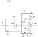
- FIG. 1 is a diagram illustrating a configuration of an imaging device.
- FIG. 2 is a diagram illustrating an image blur correction unit.
- FIG. 3 is a diagram illustrating image capture operations.
- FIG. 4 is a diagram illustrating an example of the movement of an imaging surface.
- FIG. 5 is a diagram illustrating control of a vibration-proof control unit in pixel shift image capture.
- FIG. 6 is a diagram illustrating control of the vibration-proof control unit in pixel shift image capture of the related art.
- FIG. 7 is a flow chart illustrating processing of pixel shift image capture.
- FIG. 8 is a diagram illustrating setting of an image blur correction target value.
- FIG. 9 is a diagram illustrating control of the vibration-proof control unit in pixel shift image capture.
- FIG. 1 is a diagram illustrating a configuration of an imaging device.
- An imaging device 11 in the present embodiment is a digital camera that includes an image blur correction unit 14 and can generate an image having a high resolution by performing pixel shift image capture while moving an imaging surface a predetermined shift amount.
- an image capture mode of performing so-called high-resolution image capture by synthesizing a plurality of images obtained by performing pixel shift image capture to generate a high-resolution image is referred to as a “high-resolution image capture mode.”
- a lens-interchangeable imaging device in which a lens device can be attached to and detached from a main body will be described as an example of an imaging device in the present embodiment, there is no limitation thereto, and it may be an imaging device in which the lens device and the main body are formed integrally with each other.
- the imaging device 11 includes a camera body 11 a and an interchangeable lens 11 b capable of being attached to and detached from the camera body 11 a .
- the camera body 11 a includes a camera CPU 12 a , an imaging element 14 a , a driving unit 14 b , a vibration detection unit 15 , a signal processing unit 16 , a vibration-proof control unit 17 , a still image exposure unit 18 , and an image processing unit 19 .
- the interchangeable lens 11 b is provided with an imaging optical system including a lens CPU 12 b and a focus adjustment unit 13 .
- the imaging optical system of the interchangeable lens 11 b forms an optical image of a subject on the imaging element 14 a .
- the imaging optical system includes a zoom lens that changes imaging magnification, a focus lens 13 used for focus adjustment, a plurality of lenses including a shift lens that corrects an image blur caused by a camera shake or the like, and an aperture.
- the lens CPU 12 b provided in the interchangeable lens 11 b controls a lens operation in accordance with an imaging instruction or the like from the camera body 11 a .
- the lens CPU 12 b performs focus adjustment by driving the focus lens 13 in accordance with a focus state detection signal from the camera body 11 a.
- a subject light flux along an optical axis 10 is incident on the imaging element 14 a which is an imaging unit through the imaging optical system of the interchangeable lens 11 b .
- the imaging element 14 a photoelectrically converts a subject image formed on the imaging surface through the imaging optical system, and outputs an image signal related to the subject image.
- the imaging element 14 a is, for example, a charged coupled device (CCD) or a complementary metal oxide semiconductor (CMOS) sensor.
- the driving unit 14 b drives the imaging element 14 a in a plane orthogonal to the optical axis 10 . In a high-resolution image capture mode of performing a plurality of still image exposures, the driving unit 14 b performs a pixel shift (first process) for moving the imaging surface of the imaging element 14 a in each still image exposure.
- the camera CPU 12 a provided in the camera body 11 a controls an operation of each block included in the imaging device 11 .
- the camera CPU 12 a controls an image capture operation in accordance with an imaging instruction operation or the like from a photographer, or controls an image blur correction system operation.
- the image processing unit 19 performs various types of image processing on an image signal which is output from the imaging element 14 a .
- the image processing unit 19 performs processing such as denoising, demosaicing, luminance signal conversion, aberration correction, white balance adjustment, or color correction of the image signal which is output from the imaging element 14 a , as image processing.
- the image processing unit 19 synthesizes imaging signals of images which are output by the imaging element 14 a to create a high-resolution image.
- the holding frame 14 d is provided with coils 14 p and a coil 14 y .
- the coils for example, two coils 14 p are provided on the long side of the holding frame 14 d , and one coil 14 y is provided on the short side of the holding frame 14 d .
- the coils 14 p and the coil 14 y face a permanent magnet (not shown). Therefore, the holding frame 14 d is driven in the direction of an arrow 21 p if the driving unit 14 b allows electrical conduction to the coils 14 p on the basis of the image blur correction target value from the signal processing unit 16 , and the holding frame 14 d is driven in the direction of an arrow 21 y if it allows electrical conduction to the coil 14 y.
- a total of four laminated piezoelectric members 14 e 1 to 14 e 4 are interposed between the imaging element 14 a and the holding frame 14 d , one on each side.
- the imaging element 14 a is held by the holding frame 14 d by being interposed between and supported by the four laminated piezoelectric members 14 e 1 to 14 e 4 .
- the laminated piezoelectric members 14 e 1 to 14 e 4 are piezoelectric elements for driving the imaging element 14 a in order to perform pixel shift image capture.
- the laminated piezoelectric members 14 e 1 to 14 e 4 drive the imaging element 14 a on the basis of a driving signal for pixel shift image capture.
- the imaging element 14 a is driven by the laminated piezoelectric members 14 e 1 to 14 e 4 to perform a pixel shift
- the imaging element 14 a may be driven by the coils 14 p and the coil 14 y to perform a pixel shift.
- FIG. 3 is a diagram illustrating electrical conduction to the laminated piezoelectric members.
- FIG. 4 is a diagram illustrating driving of the imaging element 14 a .
- the length shows the laminated piezoelectric members 14 e 1 to 14 e 4 .
- Pixel shifts L 1 to L 4 show the direction of movement and amount of movement of the imaging element 14 a in the pixel shifts. That is, FIG. 3 shows a voltage to be applied to each of the laminated piezoelectric members 14 e 1 to 14 e 4 for the movement of the pixel shifts L 1 to L 4 .
- a method of shifting a pixel by a half pixel in length and width with respect to a reference pixel 41 a which is the position of a pixel when a reference image is captured will be described. That is, in the high-resolution image capture mode, a total of five images of a reference image and four images captured by performing a pixel shift are acquired and synthesized. Meanwhile, a pixel shift method and the number of images to be acquired are not limited thereto.
- the imagine element 14 a is moved to a position shifted by a half pixel in length and width from the reference pixel 41 a by the pixel shift L 1 .
- the pixel shift L 1 for example, an applied voltage is applied to the laminated piezoelectric member 14 e 1 , an applied voltage +V is applied to the laminated piezoelectric member 14 e 2 , an applied voltage ⁇ V is applied to the laminated piezoelectric member 14 e 3 , and an applied voltage ⁇ V is applied to the laminated piezoelectric member 14 e 4 .
- the voltages applied to the laminated piezoelectric member 14 e 2 and the laminated piezoelectric member 14 e 3 do not change, and thus the voltage applied to the laminated piezoelectric member 14 e 2 is the applied voltage +V as it is, and the voltage applied to the laminated piezoelectric member 14 e 4 is the applied voltage ⁇ V as it is.
- pixel shift image capture can be performed by shifting the imaging element 14 a by a half pixel in length and width from the reference pixel 41 a.
- an exposure period after the movement of the pixel shift L 1 is defined as a first exposure period 51 a
- an exposure period after the movement of the pixel shift L 2 is defined as a second exposure period 51 b
- a pixel shift target value 52 shows a target value of a pixel shift in pixel shift image capture and a timing of the application of a voltage to a laminated piezoelectric member.
- a stepwise applied voltage 52 a in the pixel shift target value 52 shows a timing of the application of a voltage for performing the pixel shift L 2 between a first still image exposure period 51 a and a second still image exposure period 51 b .
- a predetermined voltage is sent to each of the laminated piezoelectric members 14 e 1 to 14 e 4 as a pixel shift target value.
- An image blur correction target value 53 is a target value of image blur correction which is given to the image blur correction unit 14 in order to perform image blur correction in the direction of the arrow 21 p in FIG. 2 .
- a current according to the image blur correction target value 53 flows to the coils 14 p , and image blur correction is performed by the coils 14 p driving the imaging element 14 a .
- the first value A is, for example, a value before a shock is generated by driving for each pixel shift image capture, that is, a value at the start of the target value fixation period 53 a.
- the target value fixation period 53 a is a period in which the imaging element 14 a is driven in accordance with the stepwise applied voltage 52 a .
- a predetermined period longer than the period in which the stepwise applied voltage 52 a is applied is set as the target value fixation period 53 a because there is a mechanical response delay or the like.
- image blur correction according to the image blur correction target value 53 is performed in the first exposure period 51 a and the second exposure period 51 b , but the image blur correction target value 53 is fixed while a pixel shift between the first exposure period 51 a and the second exposure period 51 b is performed.
- a waveform 54 is a waveform indicating the movement of the imaging surface of the imaging element 14 a .
- the imaging surface of the imaging element 14 a is driven on the basis of the pixel shift target value 52 and the image blur correction target value 53 .
- a pixel shift driving period 54 a is a period in which the pixel shift L 2 between the first still image exposure period 51 a and the second still image exposure period 51 b is performed.
- a shift width 54 b indicates the amount of movement of the imaging surface of the imaging element 14 a in the pixel shift L 2 , and one pixel's worth of movement is performed in the present embodiment.
- FIG. 6 shows each waveform in a pixel shift of the related art in which the target value fixation period 53 a is not set. Since the target value fixation period 53 a is not set in the image blur correction target value 53 in FIG. 6 , the image blur correction target value 53 is set and output in order to correct an image blur generated in the imaging element 14 a even while the imaging element 14 a is performing pixel shift driving by the stepwise applied voltage 52 a.
- the laminated piezoelectric members 14 e 1 to 14 e 4 have very high driving responsiveness. For this reason, in a case where driving of the imaging element 14 a is speeded up in order to perform pixel shift image capture, a shock associated with the driving of the imaging element 14 a is generated at the start and end of the driving for a pixel shift.
- the vibration detection unit 15 also detects a shock of pixel shift driving as the shake of the imaging element 14 a . For this reason, an error signal (a shock error) according to the shock of pixel shift driving is generated in the image blur correction target value 53 .
- a period in which the error signal is generated is an error generation period 61 a .
- the target value fixation period 53 a is provided in a period in which a shock due to the driving for performing pixel shift image capture is generated, and control is performed so that the shock error and the transient response are suppressed.
- the image blur correction target value is fixed to the first value A before a shock is generated due to the driving for performing each pixel shift image capture, and the initialized image blur correction target value is added to the first value A after a shock has converged to restart image blur correction.
- step S 703 the camera CPU 12 a fixes the image blur correction target value. Since the pixel shift driving is not performed at a point in time of step S 703 , a shock associated with the pixel shift driving is not generated, and the image blur correction target value is fixed to a value immediately before the generation of a shock.
- step S 704 the camera CPU 12 a gives an instruction for the pixel shift driving. That is, the stepwise applied voltage 52 a in FIG. 5 is output as a target value of a pixel shift.
- An image blur is also generated during the target value fixation period 53 a . Therefore, if the target value fixation period 53 a is not provided, the image blur correction target value 53 of the imaging element 14 a except for a shock error is set as in a broken-line waveform 81 in accordance with the detection result of the vibration detection unit 15 . Therefore, when the target value fixation period 53 a ends, the fixed image blur correction target value 53 shown by a solid-line waveform 82 and the broken-line waveform 81 become discontinuous, and thus a stepped difference 83 is generated. In a case where image blur correction based on the broken-line waveform 81 is performed at the end of the target value fixation period 53 a , a driving vibration according to the stepped difference 83 is generated in the image blur correction unit 14 .
- an image blur correction target value 82 initialized by the signal processing unit 16 is added to the fixed first value A.
- the image blur correction target value is configured to gradually match an actual image blur correction target value over a predetermined time (for example, 0.2 seconds).
- the initialization of an image blur correction target value corresponds to, for example, setting a history of a known IIR filter in the signal processing unit 16 to zero.
- the image blur correction unit 14 can smoothly restart the image blur correction by outputting an image blur correction target value continuously from the image blur correction target value fixed in the target value fixation period 53 a.
Abstract
Description
Claims (12)
Applications Claiming Priority (3)
| Application Number | Priority Date | Filing Date | Title |
|---|---|---|---|
| JPJP2020-004116 | 2020-01-15 | ||
| JP2020004116A JP2021111923A (en) | 2020-01-15 | 2020-01-15 | Imaging device, image blur correction method, and program |
| JP2020-004116 | 2020-01-15 |
Publications (2)
| Publication Number | Publication Date |
|---|---|
| US20210218895A1 US20210218895A1 (en) | 2021-07-15 |
| US11457161B2 true US11457161B2 (en) | 2022-09-27 |
Family
ID=76760617
Family Applications (1)
| Application Number | Title | Priority Date | Filing Date |
|---|---|---|---|
| US17/143,473 Active US11457161B2 (en) | 2020-01-15 | 2021-01-07 | Imaging device moving an imaging element a predetermined amount for each exposure to acquire a plurality of images, image blur correction method, and recording medium |
Country Status (2)
| Country | Link |
|---|---|
| US (1) | US11457161B2 (en) |
| JP (1) | JP2021111923A (en) |
Citations (4)
| Publication number | Priority date | Publication date | Assignee | Title |
|---|---|---|---|---|
| US20060087561A1 (en) * | 2004-10-26 | 2006-04-27 | Konica Minolta Photo Imaging, Inc. | Digital camera |
| US20160212332A1 (en) * | 2015-01-16 | 2016-07-21 | Mems Drive, Inc. | Three-axis ois for super-resolution imaging |
| JP2017037130A (en) | 2015-08-07 | 2017-02-16 | オリンパス株式会社 | Imaging device |
| US20170272655A1 (en) * | 2016-03-16 | 2017-09-21 | Panasonic Intellectual Property Management Co., Ltd. | Imaging device |
-
2020
- 2020-01-15 JP JP2020004116A patent/JP2021111923A/en active Pending
-
2021
- 2021-01-07 US US17/143,473 patent/US11457161B2/en active Active
Patent Citations (5)
| Publication number | Priority date | Publication date | Assignee | Title |
|---|---|---|---|---|
| US20060087561A1 (en) * | 2004-10-26 | 2006-04-27 | Konica Minolta Photo Imaging, Inc. | Digital camera |
| US20160212332A1 (en) * | 2015-01-16 | 2016-07-21 | Mems Drive, Inc. | Three-axis ois for super-resolution imaging |
| JP2017037130A (en) | 2015-08-07 | 2017-02-16 | オリンパス株式会社 | Imaging device |
| US9883107B2 (en) | 2015-08-07 | 2018-01-30 | Olympus Corporation | Imaging apparatus |
| US20170272655A1 (en) * | 2016-03-16 | 2017-09-21 | Panasonic Intellectual Property Management Co., Ltd. | Imaging device |
Also Published As
| Publication number | Publication date |
|---|---|
| JP2021111923A (en) | 2021-08-02 |
| US20210218895A1 (en) | 2021-07-15 |
Similar Documents
| Publication | Publication Date | Title |
|---|---|---|
| US8023811B2 (en) | Image capturing apparatus, control method thereof, image processing apparatus, image processing method, image capturing system, and program | |
| JP2017195516A (en) | Camera system and camera body | |
| US11223774B2 (en) | Imaging apparatus, lens apparatus, and method for controlling the same | |
| US10101593B2 (en) | Optical apparatus, control method thereof and storage medium | |
| US20110122268A1 (en) | Imaging device | |
| US10686989B2 (en) | Image stabilization apparatus, image capturing system, and method for controlling the same | |
| JP2007043584A (en) | Image pickup device and control method thereof | |
| US11570361B2 (en) | Lens unit, imaging device, control methods thereof, and storage medium | |
| US11218637B2 (en) | Image capture apparatus and control method having image stabilization which reduces peripheral light variation | |
| US11092774B2 (en) | Lens apparatus, image capturing apparatus, control method of lens apparatus, and control method of image capturing apparatus | |
| US11457161B2 (en) | Imaging device moving an imaging element a predetermined amount for each exposure to acquire a plurality of images, image blur correction method, and recording medium | |
| US11272109B2 (en) | Blur correction control apparatus, method, and storage medium | |
| US11665428B2 (en) | Lens apparatus, image pickup system, control method of lens apparatus, and storage medium | |
| US10264180B2 (en) | Image correction apparatus and method for controlling image correction apparatus | |
| US11330179B2 (en) | Imaging device and control method thereof | |
| US11575833B2 (en) | Control apparatus, image pickup apparatus, control method, and memory medium | |
| US10992867B2 (en) | Image capturing apparatus and control method thereof and storage medium | |
| JP2006330394A (en) | Autofocus device | |
| US10715715B2 (en) | Focus detection apparatus, method of controlling same, and storage medium | |
| US10681274B2 (en) | Imaging apparatus and control method thereof | |
| US20230131656A1 (en) | Image capturing apparatus and method for controlling the same, and non-transitory computer-readable storage medium | |
| WO2020012960A1 (en) | Imaging device | |
| JP6048803B2 (en) | Imaging apparatus, camera shake correction method, and program | |
| JP2021015151A (en) | Imaging device and control method of imaging device | |
| CN112119349A (en) | Imaging device, control method, and program |
Legal Events
| Date | Code | Title | Description |
|---|---|---|---|
| FEPP | Fee payment procedure |
Free format text: ENTITY STATUS SET TO UNDISCOUNTED (ORIGINAL EVENT CODE: BIG.); ENTITY STATUS OF PATENT OWNER: LARGE ENTITY |
|
| AS | Assignment |
Owner name: CANON KABUSHIKI KAISHA, JAPAN Free format text: ASSIGNMENT OF ASSIGNORS INTEREST;ASSIGNORS:NAITO, GO;WASHISU, KOICHI;REEL/FRAME:055205/0750 Effective date: 20201210 |
|
| STPP | Information on status: patent application and granting procedure in general |
Free format text: APPLICATION DISPATCHED FROM PREEXAM, NOT YET DOCKETED |
|
| STPP | Information on status: patent application and granting procedure in general |
Free format text: DOCKETED NEW CASE - READY FOR EXAMINATION |
|
| STPP | Information on status: patent application and granting procedure in general |
Free format text: NON FINAL ACTION MAILED |
|
| STPP | Information on status: patent application and granting procedure in general |
Free format text: RESPONSE TO NON-FINAL OFFICE ACTION ENTERED AND FORWARDED TO EXAMINER |
|
| STPP | Information on status: patent application and granting procedure in general |
Free format text: NOTICE OF ALLOWANCE MAILED -- APPLICATION RECEIVED IN OFFICE OF PUBLICATIONS |
|
| STCF | Information on status: patent grant |
Free format text: PATENTED CASE |