WO2019181458A1 - 抵抗測定装置、及び、抵抗測定治具 - Google Patents
抵抗測定装置、及び、抵抗測定治具 Download PDFInfo
- Publication number
- WO2019181458A1 WO2019181458A1 PCT/JP2019/008356 JP2019008356W WO2019181458A1 WO 2019181458 A1 WO2019181458 A1 WO 2019181458A1 JP 2019008356 W JP2019008356 W JP 2019008356W WO 2019181458 A1 WO2019181458 A1 WO 2019181458A1
- Authority
- WO
- WIPO (PCT)
- Prior art keywords
- wiring
- jig
- contact
- contacts
- resistance
- Prior art date
Links
Images


Classifications
-
- G—PHYSICS
- G01—MEASURING; TESTING
- G01R—MEASURING ELECTRIC VARIABLES; MEASURING MAGNETIC VARIABLES
- G01R27/00—Arrangements for measuring resistance, reactance, impedance, or electric characteristics derived therefrom
- G01R27/02—Measuring real or complex resistance, reactance, impedance, or other two-pole characteristics derived therefrom, e.g. time constant
- G01R27/14—Measuring resistance by measuring current or voltage obtained from a reference source
-
- G—PHYSICS
- G01—MEASURING; TESTING
- G01R—MEASURING ELECTRIC VARIABLES; MEASURING MAGNETIC VARIABLES
- G01R1/00—Details of instruments or arrangements of the types included in groups G01R5/00 - G01R13/00 and G01R31/00
- G01R1/02—General constructional details
- G01R1/04—Housings; Supporting members; Arrangements of terminals
- G01R1/0408—Test fixtures or contact fields; Connectors or connecting adaptors; Test clips; Test sockets
- G01R1/0416—Connectors, terminals
-
- G—PHYSICS
- G01—MEASURING; TESTING
- G01R—MEASURING ELECTRIC VARIABLES; MEASURING MAGNETIC VARIABLES
- G01R15/00—Details of measuring arrangements of the types provided for in groups G01R17/00 - G01R29/00, G01R33/00 - G01R33/26 or G01R35/00
-
- G—PHYSICS
- G01—MEASURING; TESTING
- G01R—MEASURING ELECTRIC VARIABLES; MEASURING MAGNETIC VARIABLES
- G01R27/00—Arrangements for measuring resistance, reactance, impedance, or electric characteristics derived therefrom
- G01R27/02—Measuring real or complex resistance, reactance, impedance, or other two-pole characteristics derived therefrom, e.g. time constant
-
- G—PHYSICS
- G01—MEASURING; TESTING
- G01R—MEASURING ELECTRIC VARIABLES; MEASURING MAGNETIC VARIABLES
- G01R3/00—Apparatus or processes specially adapted for the manufacture or maintenance of measuring instruments, e.g. of probe tips
-
- G—PHYSICS
- G01—MEASURING; TESTING
- G01R—MEASURING ELECTRIC VARIABLES; MEASURING MAGNETIC VARIABLES
- G01R27/00—Arrangements for measuring resistance, reactance, impedance, or electric characteristics derived therefrom
- G01R27/02—Measuring real or complex resistance, reactance, impedance, or other two-pole characteristics derived therefrom, e.g. time constant
- G01R27/08—Measuring resistance by measuring both voltage and current
-
- G—PHYSICS
- G01—MEASURING; TESTING
- G01R—MEASURING ELECTRIC VARIABLES; MEASURING MAGNETIC VARIABLES
- G01R31/00—Arrangements for testing electric properties; Arrangements for locating electric faults; Arrangements for electrical testing characterised by what is being tested not provided for elsewhere
- G01R31/36—Arrangements for testing, measuring or monitoring the electrical condition of accumulators or electric batteries, e.g. capacity or state of charge [SoC]
- G01R31/385—Arrangements for measuring battery or accumulator variables
- G01R31/3865—Arrangements for measuring battery or accumulator variables related to manufacture, e.g. testing after manufacture
Definitions
- the present invention relates to a resistance measuring device and a resistance measuring jig, and more particularly to a technique for improving the measurement accuracy of the resistance measuring device.
- the present invention has been made in view of the situation as described above, and the problem to be solved by the present invention is a resistance measuring device capable of suppressing a decrease in measurement accuracy even when noise occurs due to an external factor, And providing a resistance measuring jig.
- the present invention provides a resistance measuring device and a resistance measuring jig configured as follows.
- a resistance measuring device includes a first jig that faces one surface of a measurement object, and a plurality of second jigs that are provided on the first jig and that can contact the one surface.
- a current is supplied between the plurality of second contacts that are enabled, and the first contact and the second contact corresponding to each other, and the first contact corresponding to each other
- a voltage between the other adjacent first contact and the other second contact adjacent to the one second contact is detected, and based on the relationship between the supplied current value and the detected voltage value
- a resistance measurement unit that calculates a resistance value of the measurement object, and for each first contact, the resistance measurement unit and the first contact are connected.
- a second wiring for connecting the resistance measuring unit and the second contact from the resistance measuring unit via the vicinity of the first jig for each second contact is adjacent to each other.
- a resistance measuring device includes a first jig that faces one surface of an object to be measured, and a plurality of devices that are provided in the first jig and are capable of contacting the one surface.
- a current is supplied between the plurality of second contacts that can be brought into contact with each other, the one first contact corresponding to each other, and the one second contact corresponding to each other, and the one first contact corresponding to each other.
- a voltage between another first contactor adjacent to the child and another second contactor adjacent to the second contactor is detected, and based on the relationship between the supplied current value and the detected voltage value
- a resistance measuring unit that calculates a resistance value of the measurement object, and for each of the first contacts, the resistance measuring unit and the first contact
- a first wiring to be connected and a second wiring for connecting the resistance measurement unit and the second contact for each of the second contacts; from the resistance measurement unit to the first jig;
- the first wiring and the second wiring respectively connected to the first contact and the second contact corresponding to each other up to a predetermined location are arranged adjacent to each other, and for each first contact
- the third wiring extending from the predetermined location in the first wiring, and connected to the first contact and the second contact corresponding to each other on the tip side from the predetermined location.
- each second contact includes a fourth wiring extending from the predetermined location in the second wiring, and on the tip side from the predetermined location, The first contact and the second contact corresponding to each other Bets to those that connected the first wiring, respectively and said fourth wire are arranged adjacent.
- a resistance measurement jig is provided with a first jig that faces one surface of an object to be measured, and the first jig that can contact the one surface.
- a plurality of second contacts that can be brought into contact with each other, a first wiring connected to each of the first contacts, connected to each of the second contacts, and passing through the vicinity of the first jig.
- a first wiring connected to the first contact and the second contact corresponding to each other on the proximal side from the vicinity of the first jig, and the second wiring.
- the wiring is disposed adjacent to the wiring.
- a resistance measurement jig is provided with a first jig that faces one surface of an object to be measured, and the first jig that can contact the one surface.
- a plurality of second contacts that can be brought into contact with each other, a first wiring that is in contact with each of the first contacts, and a second that is connected to each of the second contacts and passes through the first jig.
- the first wiring and the second wiring respectively connected to the first contact and the second contact corresponding to each other on the base end side from the vicinity of the first jig. are arranged adjacent to each other, and the first jig includes a first connection member that connects the plurality of first contacts and the first wiring.
- the first connection member includes a plurality of electrodes that are in contact with the plurality of first contacts, a first wiring pattern that is connected to the electrodes and is connected to the first wiring, and a part of the second wiring.
- the first wiring pattern and the second partial pattern respectively connected to the first contact and the second contact corresponding to each other in the first connection member. Adjacent to each other.
- the conceptual diagram which shows roughly the structure of the resistance measuring apparatus which concerns on 1st embodiment.
- the block diagram which shows roughly the electrical structure of a resistance measuring apparatus.
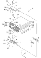
- FIG. 1 is a conceptual diagram schematically showing the configuration of a resistance measuring apparatus 1 according to the first embodiment of the present invention.
- a resistance measurement apparatus 1 shown in FIG. 1 is an apparatus that measures resistance values of tab terminals 104 and 114 of a lithium ion secondary battery 100, which is an example of an object to be measured.
- the “lithium ion secondary battery” in the present embodiment includes a work-in-process product before combining the positive electrode, separator, and negative electrode laminate and the electrolyte.
- the measuring object which measures resistance value with the resistance measuring apparatus 1 which concerns on this embodiment is not limited, It is possible to make all other conductors into a measuring object.
- a lithium ion secondary battery 100 shown in FIG. 1 has a configuration in which a plurality of positive electrode plates 101 (electrode plates) and a plurality of negative electrode plates 111 (electrode plates) are alternately stacked with a not-shown separator interposed therebetween.
- the positive electrode plate 101 is configured by applying a positive electrode active material (not shown) to the surface of a positive electrode current collector 102 made of a metal foil such as an aluminum foil.
- the negative electrode plate 111 is configured by applying a negative electrode active material (not shown) to the surface of a negative electrode current collector 112 made of a metal foil such as a copper foil.
- each positive electrode current collector 102 is drawn out as a tab portion 103 (a part of a sheet or an electrode plate) on one end side of the lithium ion secondary battery 100, and a part of each negative electrode current collector 112 is a tab. It is drawn out as a part 113 (a sheet, a part of the electrode plate).
- Each tab portion 103 is pulled out toward one side of the one end, and each tab portion 113 is pulled out toward the opposite side to the tab portion 103. Thereby, the tab part 103 and the tab part 113 are made not to overlap.
- the tab portions 103 are laminated and adhered to each other, and are welded to each other in a welding region 105 indicated by a strip-shaped netting to form a positive tab terminal 104.
- the tab portions 113 are laminated and adhered to each other, and are welded to each other at a welding region 115 indicated by a strip-shaped netting to form a negative tab terminal 114 (sheet member, tab terminal).
- Various welding methods can be applied as the welding method of the welding regions 105 and 115, and for example, ultrasonic welding is used. In FIG. 1, the state before each tab part 103 and 113 is welded is shown.
- the resistance measurement apparatus 1 shown in FIG. 1 holds the detection units 4U and 4D, the resistance measurement unit 5, the notification unit 6, and the lithium ion secondary battery 100 to be inspected at a predetermined position between the detection units 4U and 4D.
- the detection units 4U and 4D include first and second jigs 3U and 3D, which are detection jigs, respectively.
- the detection units 4U and 4D are configured to be able to move the first and second jigs 3U and 3D in the Z-axis direction (a direction substantially perpendicular to the main surfaces of the tab terminals 104 and 114) by a drive mechanism (not shown). Yes.
- the detection units 4U and 4D may be movable in three axis directions of X, Y, and Z orthogonal to each other, and the first and second jigs 3U and 3D can be rotated around the Z axis. May be.
- the notification unit 6 is a notification device that visually notifies the user of the information obtained by the resistance measurement unit 5.
- a display device such as a liquid crystal display device or a printer can be used.
- the detection unit 4U is located above the lithium ion secondary battery 100 fixed to a battery holding unit (not shown).
- the detection unit 4U is configured to be detachable from a first jig 3U that is a detection jig for sequentially bringing the probe Pu into contact with the tab terminals 104, 114 of the lithium ion secondary battery 100.
- the first jig 3U is provided so as to face the upper surface of the tab terminals 104, 114 (positive Z-axis direction side, the same applies hereinafter).
- the detection unit 4D is located below the lithium ion secondary battery 100 fixed to a battery holding unit (not shown).
- the detection unit 4D is configured to be detachable from a second jig 3D, which is a detection jig for sequentially bringing the probe Pd into contact with the tab terminals 104 and 114 of the lithium ion secondary battery 100.
- the second jig 3D is provided to face the lower surface (the negative Z-axis direction side, the same applies hereinafter) of the tab terminals 104 and 114.
- the first and second jigs 3U and 3D are configured in the same manner except that the mounting directions to the detection units 4U and 4D are upside down.
- the first and second jigs 3U and 3D may be configured such that the tab terminals 104 and 114 are brought into contact with the two tab terminals 104 and 114 at the same time with the probes Pu and Pd.
- a probe attached to the first jig 3U located above is referred to as a probe Pu
- a probe attached to the second jig 3D located below is referred to as a probe Pd.
- the detection units 4U and 4D are collectively referred to as the detection unit 4
- the probes Pu and Pd are collectively referred to as the probe P.
- Each of the first and second jigs 3U and 3D includes a support member 31 that holds the tips of the plurality of probes Pu and Pd toward the welding regions 105 and 115 of the tab terminals 104 and 114, and a base plate 321. Yes.
- the base plate 321 is provided with unillustrated electrodes that are in contact with the rear end portions of the probes Pu and Pd to be conductive.
- the detection units 4U and 4D electrically connect the probes Pu and Pd to the power supply circuit 51 and the voltage circuit 52 of the resistance measurement unit 5 through the electrodes of the base plate 321 and a connection circuit 41 described later. Switch the connection.
- the probes Pu and Pd have a substantially rod-like shape as a whole.
- the support member 31 is formed with a plurality of through holes that support the probes Pu and Pd.
- the support member 31 has a shape and a size corresponding to the welding regions 105 and 115.
- the support member 31 supports the probes Pu and Pd so that the plurality of probes Pu and Pd are brought into contact with the welding region 105 or substantially the entire region in the welding region 115 with a substantially uniform distribution.
- the plurality of probes Pu and Pd are arranged so as to correspond to the intersection position of the lattice, for example.
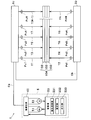
- FIG. 2 is a block diagram conceptually showing the electrical configuration of the resistance measuring apparatus 1 shown in FIG.
- the resistance measurement apparatus 1 shown in FIG. 2 includes M probes Pu1 to PuM provided on the first jig 3U, M probes Pd1 to PdM provided on the second jig 3D, a resistance measurement unit 5, and a proximal end side.
- a wiring band Ca and a tip-side wiring band Cb are provided.
- FIG. 2 shows a state in which the probes Pu1 to PuM and Pd1 to PdM are brought into contact with the tab terminal 104.
- the proximal end side wiring band Ca is an assembly of wirings connecting the first jig 3U and the connection circuit 41 of the resistance measuring unit 5 (see FIG. 3).
- the distal end side wiring band Cb is an assembly of wirings connecting the first jig 3U and the second jig 3D (see FIG. 3).
- the resistance measurement unit 5 includes a connection circuit 41, a power supply circuit 51, a voltage detection unit 52, a control unit 53, and the like.
- the configuration (the first jig 3U, the second jig 3D, the base end side wiring band Ca, and the front end side wiring band Cb) excluding the resistance measuring unit 5 from the resistance measuring device 1 is generically named. Will be described as “resistance measuring jig”.
- the resistance measuring apparatus 1 is configured to be able to remove the resistance measuring jig and replace it with another resistance measuring jig according to the type of the lithium ion secondary battery 100 to be inspected.
- the tab terminal 104 shown in FIG. 2 is shown in a cross section obtained by cutting the tab terminal 104 shown in FIG. 1 along the X-axis direction.
- Probes Pu1 to PuM and Pd1 to PdM are obtained by attaching a probe number to each row of probes Pu and Pd aligned along the X-axis direction.
- the probe numbers given to the probes Pu and Pd correspond to the X coordinate in the X-axis direction indicating the position of the welding region 105 in contact with each probe P. That is, probes Pu and Pd having the same probe number are provided correspondingly at the same position.
- Probes Pu and Pd are provided in a plurality of rows adjacent to each other in the Y-axis direction in addition to the probe P shown in FIG.
- the number of the column corresponds to the Y coordinate in the Y-axis direction that indicates the position of the welding region 105 in contact with each probe P.
- Each row of the probes P does not necessarily have to be a straight row, and may be a row that is zigzag, bent, or scattered.
- Each probe P is provided with a contact T for a four-terminal measurement method.
- the probes Pu1, Pu2, Pu3, Pu4,... PuM provided on the first jig 3U are in contact with the upper surfaces of the tab terminals 104, 114.
- Children T1, T3, T5, T7... T (N-1) are provided.
- N is a number (even number) corresponding to twice M.
- the probes Pd1, Pd2, Pd3, Pd4,... PdM provided on the second jig 3D and corresponding to the probes Pu1, Pu2, Pu3, Pu4,.
- the contacts T1, T3, T5, T7... T (N-1) provided in the first jig 3U are collectively referred to as “first contacts”.
- T2, T4, T6, T8... TN provided in the second jig 3D are collectively referred to as “second contactor”.
- each probe may have a configuration including two contacts for current supply and voltage measurement.
- a coaxial probe composed of one contact having a shape and another contact inserted into the one contact can be used.
- each of the rod-shaped probes arranged in a lattice shape may be used as a contact, and two probes (contacts) may be used as a set and used as one probe.
- the first contacts T1, T3, T5, T7... T (N-1) provided in the first jig 3U are connected to the connection circuit 41 of the resistance measuring unit 5 through the proximal end side wiring band Ca.
- the base end side wiring band Ca is a first connecting the connection circuit 41 with each of the first contacts T1, T3, T5, T7... T (N ⁇ 1).
- Wirings C1, C3, C5, C7... C (N ⁇ 1) are provided.
- the first wirings C1, C3, C5, C7... C (N-1) are collectively referred to as “first wiring group CA1”.
- the second contacts T2, T4, T6, T8,... TN provided in the second jig 3D are connected to the connection circuit 41 of the resistance measuring unit 5 through the proximal end side wiring band Ca and the distal end side wiring band Cb. Is done. Specifically, as shown in FIG. 3, the proximal end side wiring band Ca and the distal end side wiring band Cb are connected to the connection circuit 41 and the second contacts T2, T4, T6, T8. Two wirings C2, C4, C6, C8... CN are provided.
- the second wirings C2, C4, C6, C8... CN are collectively referred to as “second wiring group CA2”.
- the first contacts T1, T3, T5, T7... T (N-1) provided in the first jig 3U are connected to the second jig 3D through the tip end side wiring band Cb.
- the distal end side wiring band Cb is connected to the first contacts T1, T3, T5... T (N-1) and the first wirings C1, C3, C5. , C7... C (N ⁇ 1) and third wirings Cb1, Cb3, Cb5, Cb7.
- Each of the third wirings Cb1, Cb3, Cb5, Cb7... Cb (N ⁇ 1) is not electrically connected in the second jig 3D but is an open end.
- third wiring group CB1 (N ⁇ 1) are collectively referred to as “third wiring group CB1”. As shown in the second embodiment in FIG. 5, the open end of the third wiring group CB1 may be separated from the second jig 3D as long as it is close to the second jig 3D.
- each of the second contacts T2, T4, T6, T8... TN provided in the second jig 3D has a first wiring group CA1 and a second wiring group CA2 branched as shown in FIG. It is connected to the fourth wirings Cb2, Cb4, Cb6, Cb8... CbN provided in the first jig 3U on the tip side from the location.
- the fourth wirings Cb2, Cb4, Cb6, Cb8... CbN are branched and extended from the second wirings C2, C4, C6, C8.
- Each of the fourth wirings Cb2, Cb4, Cb6, Cb8... CbN is not electrically connected in the first jig 3U and is an open end.
- fourth wirings Cb2, Cb4, Cb6, Cb8... CbN are collectively referred to as “fourth wiring group CB2”.
- the open end of the fourth wiring group CB2 may be separated from the first jig 3U as long as it is close to the first jig 3U.
- connection circuit 41 is configured using, for example, a plurality of switching elements.
- the connection circuit 41 selects a pair of probes Pu and Pd (one probe Pu and Pd) corresponding to each other with the tab terminal 104 interposed therebetween according to a control signal from the control unit 53. Then, the positive electrode of the power circuit 51 is connected to the first contact T of the selected one probe Pu, and the negative electrode of the power circuit 51 is connected to the second contact T of the one probe Pd corresponding to the one probe Pu. Connecting. For example, when the probes Pu1 and Pd1 are selected as one probe Pu and Pd, the first contact T1 and the second contact T2 are connected to the power supply circuit 51.
- connection circuit 41 corresponds to each other with the tab terminal 104 interposed therebetween in accordance with a control signal from the control unit 53, and a pair of probes Pu, Pd (others) adjacent to the one probe Pu and the one probe Pu. Probes Pu, Pd). Then, the positive electrode of the voltage circuit 52 is connected to the first contact T of the other selected probe Pu, and the negative electrode of the voltage circuit 52 is connected to the second contact T of the probe Pd corresponding to the other probe Pu. .
- the probes Pu1 and Pd1 are selected as the one probes Pu and Pd
- the probes Pu2 and Pd2 are selected as the other probes Pu and Pd
- the voltage circuit 52 includes the first contact T3 and the second contact T4. Can be connected to.
- the power circuit 51 is a constant current power circuit such as a switching power circuit.
- the power supply circuit 51 corresponds to the first contacts T1, T3, T5... T (N-1) and the second contacts T2, T4, T6.
- a constant DC current I set in advance is supplied between the TN (for example, between the contact T1 of the probe Pu1 and the contact T2 of the probe Pd1).
- the voltage detection unit 52 is a voltage measurement circuit configured using, for example, a voltage dividing resistor or an analog-digital converter.
- the voltage detector 52 selects the first contacts T1, T3, T5... T (N ⁇ 1) and the second contacts T2, T2 corresponding to each other in the pair of probes Pu and Pd selected by the connection circuit 41.
- the voltage V between T4, T6... TN (for example, between the contact T3 of the probe Pu2 and the contact T4 of the probe Pd2) is measured, and the measured value is transmitted to the control unit 53.
- the control unit 53 includes, for example, a CPU (Central Processing Unit) that executes predetermined arithmetic processing, a RAM (Random Access Memory) that temporarily stores data, a storage device that stores a predetermined control program, and peripheral circuits thereof And so on. And the control part 53 functions as the detection control part 531, the measurement part 532, and the output part 533 by executing the above-mentioned control program, for example.
- a CPU Central Processing Unit
- RAM Random Access Memory
- the detection control unit 531 controls the drive mechanism (not shown) to move and position the detection units 4U and 4D, and sequentially contacts the tips of the probes Pu and Pd to the welding regions 105 and 115 of the lithium ion secondary battery 100.
- the first and second jigs 3U and 3D are provided with the number of probes Pu and Pd that can simultaneously contact the welding regions 105 and 115, and the probes Pu and Pd are simultaneously brought into contact with the welding regions 105 and 115. Also good.
- each probe P includes a contact T, and current supply and voltage measurement are performed by different contacts T. Therefore, resistance measurement by a four-terminal measurement method is possible.
- the measurement unit 532 is a tab terminal between the probes Pu and Pd (for example, probes Pu1 and Pd1) corresponding to each other based on the relationship between the current value supplied by the power supply circuit 51 and the voltage value detected by the voltage detection unit 52.
- the resistance values 104 and 114 are calculated.
- the output unit 533 causes the notification unit 6 to output the resistance value calculated by the measurement unit 532.
- the connection circuit 41 changes the probes Pu and Pd to be selected, and calculates resistance values in order for the corresponding probes Pu and Pd. At this time, the probes Pu and Pd functioned for supplying current in one inspection step are functioned for voltage measurement in the next inspection step.
- the connection circuit 41 when the contact T1 is electrically connected to the power supply circuit 51, the contact T1 functions as a current supply (in this case, the first wiring C1 functions as a current supply wiring).
- the contact T1 when the same contact T1 is electrically connected to the voltage detector 52, the contact T1 functions as a voltage measurement (in this case, the first wiring C1 functions as a voltage measurement wiring). According to this configuration, it is possible to obtain the number of measurement points substantially equal to the number M of the contacts T provided in the first jig 3U.
- a first wiring group CA1 connected to the first contacts T1, T3, T5... T (N-1) and the second contacts T2, T4, T6.
- the second wiring group CA2 is disposed adjacent to the second wiring group CA2. Specifically, first wirings C1, C3, C5, C7... C (N-1) connected to the first contacts T1, T3, T5. Second wirings C2, C4, C6, C8... CN connected to the second contacts T2, T4, T6, T8... TN are arranged adjacent to the corresponding positions.
- the gap between the resistance measurement unit 5 and the first jig 3U (the basis of the first jig 3U).
- the first wiring and the second wiring (for example, the first wiring) respectively connected to the first contact and the second contact (for example, the first contact T1 and the second contact T2) corresponding to each other.
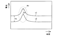
- C1 and the second wiring C2) are arranged adjacent to each other. For this reason, noise due to the electromagnetic influence received from the outside is generated in substantially the same magnitude in the adjacent wiring.
- the second wiring group CA2 includes the resistance measuring unit 5 and the second contacts T2, T4, T6, T8 for each of the second contacts T2, T4, T6, T8. ... TN is connected from the resistance measuring unit 5 via the vicinity of the first jig 3U.
- the second wiring group CA2 is configured to branch from the first wiring group CA1 in the first jig 3U.
- the portion where the second wiring group CA2 branches from the first wiring group CA1 may be separated from the first jig 3U as long as it is in the vicinity of the first jig 3U.
- “in the vicinity of the first jig 3U” in the present embodiment is used to mean both the “first jig 3U” and the “location spaced close to the first jig 3U”. ing.
- the tip side connecting the first jig 3U and the second jig 3D the tip side connecting the first jig 3U and the second jig 3D.
- CB1 and second wiring group CA2 are arranged adjacent to each other.
- Second wirings C2, C4, C6, C8... CN connected to the second contacts T2, T4, T6, T8... TN are arranged adjacent to the corresponding positions.
- the first corresponding to each other between the first jig 3U and the second jig 3D.
- Adjacent the third wiring and the second wiring (for example, the third wiring Cb1 and the second wiring C2) respectively connected to the contact and the second contact (for example, the first contact T1 and the second contact T2).
- the noise by the electromagnetic influence which a 2nd wiring receives from the outside will arise with the substantially the same magnitude
- the fall of the measurement precision in the resistance measuring apparatus 1 can be suppressed.
- the first wiring group CA1 and the second wiring group CA2 are more branched than the portion.
- the first wiring group CA1 and the fourth wiring group CB2 are disposed adjacent to each other. Specifically, first wirings C1, C3, C5, C7,... C (N-1) connected to the first contacts T1, T3, T5. , Fourth wires Cb2, Cb4, Cb6, Cb8... CbN connected to the second contacts T2, T4, T6, T8... TN, respectively, are arranged adjacent to the corresponding positions. .
- the first wiring and the fourth wiring (for example, the first wiring) respectively connected to the first contact and the second contact (for example, the first contact T1 and the second contact T2) corresponding to each other.
- One wiring C1 and fourth wiring Cb2) are arranged adjacent to each other. For this reason, the noise by the electromagnetic influence which a 1st wiring receives from the outside will arise with the substantially same magnitude
- noise generated in the first wiring is similarly generated in the fourth wiring and transmitted to the second wiring, so that the influence of noise can be reduced.
- noise generated in the first wiring is similarly generated in the fourth wiring and transmitted to the second wiring, so that the influence of noise can be reduced.
- the second wiring group CA2 in FIG. 5 if the configuration includes all of the first wiring group CA1, the second wiring group CA2, the third wiring group CB1, and the fourth wiring group CB2, the second wiring The location where the group CA2 branches from the first wiring group CA1 does not have to be near the first jig 3U. That is, in the present embodiment, a predetermined portion (the second wiring group CA2 in FIG. 5 is separated from the first jig 3U between the resistance measurement unit 5 (see FIG. 2) and the first jig 3U.
- the first wiring group CA1 and the second wiring group CA2 connected to each other are arranged adjacent to each other.
- the connected third wiring group CB1 and second wiring group CA2 are arranged adjacent to each other. Further, the first contacts T1, T3, T5... T (N-1) and the second contacts T2, T4, T6, T8.
- the connected first wiring group CA1 and fourth wiring group CB2 are arranged adjacent to each other.
- the first wiring and the second wiring are disposed adjacent to each other up to a predetermined location
- the third wiring and the second wiring are disposed adjacent to each other on the tip side from the predetermined location
- the first wiring and the fourth wiring are arranged adjacent to each other, even when noise due to an external factor is generated in each wiring, the adjacent wiring is generated in substantially the same size. That is, noise generated in one wiring is also generated and transmitted to the adjacent wiring in the same manner, so that the influence of noise can be reduced. Thereby, even when noise occurs due to an external factor in any wiring, it is possible to suppress a decrease in measurement accuracy in the resistance measuring apparatus 1.
- the open end of the third wiring group CB1 may reach the second jig 3D.
- a PCB (Printed Circuit Board) interposer such as a second connection member described later
- a second wiring pattern and a third wiring pattern having an open end are disposed adjacent to each other, and the front end of the second wiring group CA2
- noise is generated in the second jig 3D due to an external factor because part of the side is constituted by the second wiring pattern and part of the tip side of the third wiring group CB1 is constituted by the third wiring pattern.
- a decrease in measurement accuracy in the resistance measuring apparatus 1 can be suppressed.
- the open end of the fourth wiring group CB2 may reach the first jig 3U, and the adjacent wiring patterns are connected to the tips of the first wiring group CA1 and the fourth wiring group CB2 in the same manner as the PCB interposer. It may be configured as part of the side.
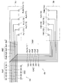
- the resistance measurement jig in the present embodiment is different from the configuration of the resistance measurement jig according to the first embodiment in that the first jig 3U includes a first connection member 3cU and the second jig 3D includes a first connection member 3cU as shown in FIG. The difference is that the second connection member 3cD is provided.
- the same components as those in the first embodiment are denoted by the same reference numerals, and detailed description thereof is omitted.
- first jig 3U may include the first connection member 3cU, and the second jig 3D may not include the second connection member 3cD. Conversely, only the second jig 3D may include the second connection member 3cD, and the first jig 3U may not include the first connection member 3cU.
- the first connection member 3cU and the second connection member 3cD are configured by a PCB interposer, and various wiring patterns (first to fourth wiring patterns P1 to P4 and first to fourth wirings as will be described in detail later) are formed therein.
- a two-part pattern Pp2) is formed.
- the first connection member 3cU and the second connection member 3cD are connected to various wiring groups by the connectors CN1 to CN3.
- the first connecting member 3cU connects the first contacts T1, T3, T5, T7... T (N-1) and the first wirings C1, C3, C5, C7. To do.
- the second connection member 3cD connects the second contacts T2, T4, T6, T8... TN and the second wirings C2, C4, C6, C8.
- the first connection member 3cU includes a plurality of electrodes E1, E3, E5, E7 with which the first contacts T1, T3, T5, T7... T (N-1) are in contact. ... E (N-1) and these electrodes E1, E3, E5, E7 ... E (N-1) and the first wirings C1, C3, C5, C7 ... C (N -1) and a second partial pattern Pp2 constituting a part of the second wirings C2, C4, C6, C8... CN.
- the first connection member 3cU further includes a fourth wiring pattern P4 extending from the second partial pattern Pp2.
- the second connecting member 3cD includes a plurality of electrodes E2, E4, E6, E8... EN with which the second contacts T2, T4, T6, T8. Are connected to the second wirings C2, C4, C6, C8... CN, and the third wirings Cb1, Cb3, Cb5 are connected to the electrodes E2, E4, E6, E8. And a third wiring pattern P3 connected to Cb7... Cb (N ⁇ 1).
- a first wiring pattern P1 and a second partial pattern Pp2 respectively connected to TN are arranged adjacent to each other.
- the first wiring pattern P1 and the second partial pattern Pp2 are disposed adjacent to each other, so that noise due to an external factor is generated on the proximal end side in the first connection member 3cU. Even in this case, a decrease in measurement accuracy can be suppressed.
- a third wiring pattern P3 and a second wiring pattern P2 respectively connected to TN are disposed adjacent to each other.
- the third wiring pattern P3 and the second wiring pattern P2 are arranged adjacent to each other in the second connection member 3cD, even when noise due to external factors occurs in the second connection member 3cD, the measurement accuracy is increased. Can be suppressed.
- the first contacts T1, T3, T5... T (N-1) and the second contacts T2, T4, T6 are arranged adjacent to each other.
- the first wiring pattern P1 and the fourth wiring pattern P4 are disposed adjacent to each other, so that the first wiring pattern P1 and the second partial pattern Pp2 are branched from each other. Even if noise due to external factors occurs on the tip side, it is possible to suppress a decrease in measurement accuracy.
- a resistance measuring device includes a first jig that faces one surface of an object to be measured, and a plurality of devices that are provided in the first jig and are capable of contacting the one surface.
- a current is supplied between the plurality of second contacts that can be brought into contact with each other, the one first contact corresponding to each other, and the one second contact corresponding to each other, and the one first contact corresponding to each other.
- a voltage between another first contactor adjacent to the child and another second contactor adjacent to the second contactor is detected, and based on the relationship between the supplied current value and the detected voltage value
- a resistance measuring unit that calculates a resistance value of the measurement object, and for each of the first contacts, the resistance measuring unit and the first contact A first wiring to be connected, and a second wiring for connecting the resistance measurement unit and the second contactor from the resistance measurement unit via the vicinity of the first jig for each second contact.
- the first wiring and the second wiring respectively connected to the first contact and the second contact corresponding to each other between the resistance measurement unit and the first jig are adjacent to each other. Are arranged.
- the first wiring and the second wiring are arranged adjacent to each other, even if noise due to an external factor occurs between the resistance measurement unit and the first jig, the measurement accuracy is reduced. Can be suppressed.
- the resistance measuring device further includes a third wiring extending from the first wiring for each of the first contacts, and corresponds to each other between the first jig and the second jig. It is preferable that the third wiring and the second wiring respectively connected to the first contact and the second contact are disposed adjacent to each other.
- the third wiring and the second wiring are arranged adjacent to each other, even if noise due to an external factor occurs between the first jig and the second jig, the measurement accuracy is lowered. Can be suppressed.
- the resistance measuring device further includes a fourth wiring extending from the second wiring for each of the second contacts, and on a tip side of a portion where the first wiring and the second wiring branch.
- the first wiring and the fourth wiring connected to the first contact and the second contact corresponding to each other are preferably disposed adjacent to each other.
- the first wiring and the fourth wiring are arranged adjacent to each other, even when noise due to an external factor occurs on the tip side from the position where the first wiring and the second wiring branch. A decrease in measurement accuracy can be suppressed.
- a resistance measuring device includes a first jig that faces one surface of an object to be measured, and a plurality of devices that are provided in the first jig and are capable of contacting the one surface.
- a current is supplied between the plurality of second contacts that can be brought into contact with each other, the one first contact corresponding to each other, and the one second contact corresponding to each other, and the one first contact corresponding to each other.
- a voltage between another first contactor adjacent to the child and another second contactor adjacent to the second contactor is detected, and based on the relationship between the supplied current value and the detected voltage value
- a resistance measuring unit that calculates a resistance value of the measurement object, and for each of the first contacts, the resistance measuring unit and the first contact
- a first wiring to be connected and a second wiring for connecting the resistance measurement unit and the second contact for each of the second contacts; from the resistance measurement unit to the first jig;
- the first wiring and the second wiring respectively connected to the first contact and the second contact corresponding to each other up to a predetermined location are arranged adjacent to each other, and for each first contact
- the third wiring extending from the predetermined location in the first wiring, and connected to the first contact and the second contact corresponding to each other on the tip side from the predetermined location.
- each second contact includes a fourth wiring extending from the predetermined location in the second wiring, and on the tip side from the predetermined location, The first contact and the second contact corresponding to each other Bets to those that connected the first wiring, respectively and said fourth wire are arranged adjacent.
- the first wiring and the second wiring are disposed adjacent to each other up to a predetermined location
- the third wiring and the second wiring are disposed adjacent to each other on the tip side from the predetermined location
- the first wiring and the fourth wiring are arranged adjacent to each other, it is possible to suppress a decrease in measurement accuracy even when noise due to an external factor occurs in each wiring.
- a resistance measurement jig is provided with a first jig that faces one surface of an object to be measured, and the first jig that can contact the one surface.
- a plurality of second contacts that can be brought into contact with each other, a first wiring connected to each of the first contacts, connected to each of the second contacts, and passing through the vicinity of the first jig.
- a first wiring connected to the first contact and the second contact corresponding to each other on the proximal side from the vicinity of the first jig, and the second wiring.
- the wiring is disposed adjacent to the wiring.
- the first wiring and the second wiring are arranged adjacent to each other, even when noise due to an external factor is generated on the proximal side from the vicinity of the first jig, the measurement accuracy is reduced. Can be suppressed.
- the resistance measuring jig further includes a third wiring extending from the first wiring for each of the first contacts, and corresponds to each other between the first jig and the second jig.
- the third wiring and the second wiring connected to the first contact and the second contact are arranged adjacent to each other.
- the third wiring and the second wiring are arranged adjacent to each other, even if noise due to an external factor occurs between the first jig and the second jig, the measurement accuracy is lowered. Can be suppressed.
- the resistance measurement jig further includes a fourth wiring extending from the second wiring for each of the second contacts, and is more distal than a portion where the first wiring and the second wiring branch.
- the first wiring and the fourth wiring connected to the first contact and the second contact corresponding to each other are preferably disposed adjacent to each other.
- the first wiring and the fourth wiring are arranged adjacent to each other, even when noise due to an external factor occurs on the tip side from the position where the first wiring and the second wiring branch. A decrease in measurement accuracy can be suppressed.
- a resistance measurement jig is provided with a first jig that faces one surface of an object to be measured, and the first jig that can contact the one surface.
- a plurality of second contacts that can be brought into contact with each other, a first wiring that is in contact with each of the first contacts, and a second that is connected to each of the second contacts and passes through the first jig.
- the first wiring and the second wiring respectively connected to the first contact and the second contact corresponding to each other on the base end side from the vicinity of the first jig. are arranged adjacent to each other, and the first jig includes a first connection member that connects the plurality of first contacts and the first wiring.
- the first connection member includes a plurality of electrodes that are in contact with the plurality of first contacts, a first wiring pattern that is connected to the electrodes and is connected to the first wiring, and a part of the second wiring.
- the first wiring pattern and the second partial pattern respectively connected to the first contact and the second contact corresponding to each other in the first connection member. Adjacent to each other.
- the first wiring pattern and the second partial pattern are arranged adjacent to each other in the first connection member, even when noise due to an external factor occurs on the proximal end side of the first connection member. A decrease in measurement accuracy can be suppressed.
- the resistance measuring jig further includes a third wiring extending from the first wiring for each of the first contacts, and corresponds to each other between the first jig and the second jig.
- the third wiring and the second wiring respectively connected to the first contact and the second contact are arranged adjacent to each other, and the second jig includes the plurality of second contacts and
- the second connection member is connected to the second wiring, and the second connection member is connected to the plurality of electrodes that are in contact with the plurality of second contacts, and is connected to the electrodes and connected to the second wiring.
- a second wiring pattern connected to the third wiring, and the second connection member connected to the first contact and the second contact corresponding to each other.
- the third wiring pattern and the second wiring pattern are adjacent to each other. It is preferred that the.
- the third wiring pattern and the second wiring pattern are arranged adjacent to each other in the second connection member, even when noise due to an external factor occurs in the second connection member, the measurement accuracy decreases. Can be suppressed.
- the first connection member further includes a fourth wiring pattern extending from the second partial pattern, and the first wiring pattern and the second partial pattern of the first connection member.
- the first wiring pattern and the fourth wiring pattern connected to the first contactor and the second contactor corresponding to each other are arranged adjacent to each other on the tip side of the branching point. It is preferable.
- the first wiring pattern and the fourth wiring pattern are arranged adjacent to each other in the first connection member, the first wiring pattern and the second partial pattern are branched at the first connection member. Even when noise due to an external factor occurs on the tip side from the location, it is possible to suppress a decrease in measurement accuracy.
- Resistance measurement device 3 Detection jig 3D second jig 3U first jig 3cD second connection member 3cU first connection member 4 detector 4D detector 4U detection unit 5 resistance measurement unit 6 Informing part 31 Support member 41 Connection circuit 51 Power supply circuit 52 Voltage Detection Unit 53 Control Unit 100 Lithium ion secondary battery 101 Positive electrode plate 102 Positive electrode current collector 103 Tab section 104 Tab terminal 105 Welding area 111 Negative electrode plate 112 Negative electrode current collector 113 Tab portion 114 Tab terminal 115 Welding area 321 Base plate 531 Detection control unit 532 Measuring unit 533 Output unit Ca Base side wiring band Cb Tip side wiring band C1 to CN wiring Cb1 to CbN wiring CA1 first wiring group CA2 second wiring group CB1 Third wiring group CB2 Fourth wiring group I DC current Nv Noise component P probe P1 to P4 Wiring pattern Pp2 Partial pattern Pd probe Pu probe V voltage Vc Potential difference Vn Potential difference
Abstract
Description
3D 第二治具 3U 第一治具
3cD 第二接続部材 3cU 第一接続部材
4 検出部 4D 検出部
4U 検出部 5 抵抗測定部
6 報知部 31 支持部材
41 接続回路 51 電源回路
52 電圧検出部 53 制御部
100 リチウムイオン二次電池
101 正極板 102 正極集電体
103 タブ部 104 タブ端子
105 溶着領域 111 負極板
112 負極集電体 113 タブ部
114 タブ端子 115 溶着領域
321 ベースプレート 531 検出制御部
532 測定部 533 出力部
Ca 基端側配線帯 Cb 先端側配線帯
C1~CN 配線 Cb1~CbN 配線
CA1 第一配線群 CA2 第二配線群
CB1 第三配線群 CB2 第四配線群
I 直流電流 Nv ノイズ成分
P プローブ P1~P4 配線パターン
Pp2 部分パターン Pd プローブ
Pu プローブ V 電圧
Vc 電位差 Vn 電位差
Claims (10)
- 測定対象物の一方の面に対向する第一治具と、
前記第一治具に備えられて前記一方の面に当接可能とされる複数の第一接触子と、
前記測定対象物の他方の面に対向する第二治具と、
前記第二治具において複数の前記第一接触子にそれぞれ対応して備えられて前記他方の面に当接可能とされる複数の第二接触子と、
互いに対応する一の前記第一接触子と一の前記第二接触子との間に電流を供給し、互いに対応する前記一の第一接触子に隣接する他の第一接触子と前記一の第二接触子に隣接する他の第二接触子との間の電圧を検出し、供給した電流値と検出した電圧値との関係に基づいて前記測定対象物の抵抗値を算出する抵抗測定部と、
前記第一接触子ごとに、前記抵抗測定部と前記第一接触子とを接続する第一配線と、
前記第二接触子ごとに、前記抵抗測定部と前記第二接触子とを、前記抵抗測定部から前記第一治具の近傍を経由して接続する第二配線とを備え、
前記抵抗測定部と前記第一治具との間において、互いに対応する前記第一接触子と前記第二接触子とにそれぞれ接続された前記第一配線と前記第二配線とが隣接して配置される、抵抗測定装置。 - 前記第一接触子ごとに、前記第一配線から延出される第三配線をさらに備え、
前記第一治具と前記第二治具との間において、互いに対応する前記第一接触子と前記第二接触子とにそれぞれ接続された前記第三配線と前記第二配線とが隣接して配置される、請求項1に記載の抵抗測定装置。 - 前記第二接触子ごとに、前記第二配線から延出される第四配線をさらに備え、
前記第一配線と前記第二配線とが枝分かれする箇所よりも先端側において、互いに対応する前記第一接触子と前記第二接触子とにそれぞれ接続された前記第一配線と前記第四配線とが隣接して配置される、請求項1又は請求項2に記載の抵抗測定装置。 - 測定対象物の一方の面に対向する第一治具と、
前記第一治具に備えられて前記一方の面に当接可能とされる複数の第一接触子と、
前記測定対象物の他方の面に対向する第二治具と、
前記第二治具において複数の前記第一接触子にそれぞれ対応して備えられて前記他方の面に当接可能とされる複数の第二接触子と、
互いに対応する一の前記第一接触子と一の前記第二接触子との間に電流を供給し、互いに対応する前記一の第一接触子に隣接する他の第一接触子と前記一の第二接触子に隣接する他の第二接触子との間の電圧を検出し、供給した電流値と検出した電圧値との関係に基づいて前記測定対象物の抵抗値を算出する抵抗測定部と、
前記第一接触子ごとに、前記抵抗測定部と前記第一接触子とを接続する第一配線と、
前記第二接触子ごとに、前記抵抗測定部と前記第二接触子とを接続する第二配線と、を備え、
前記抵抗測定部から、前記第一治具との間の所定箇所まで、互いに対応する前記第一接触子と前記第二接触子とにそれぞれ接続された前記第一配線と前記第二配線とが隣接して配置され、
前記第一接触子ごとに、前記第一配線における前記所定箇所から延出される第三配線を備え、
前記所定箇所よりも先端側において、互いに対応する前記第一接触子と前記第二接触子とにそれぞれ接続された前記第三配線と前記第二配線とが隣接して配置され、
前記第二接触子ごとに、前記第二配線における前記所定箇所から延出される第四配線を備え、
前記所定箇所よりも先端側において、互いに対応する前記第一接触子と前記第二接触子とにそれぞれ接続された前記第一配線と前記第四配線とが隣接して配置される、抵抗測定装置。 - 測定対象物の一方の面に対向する第一治具と、
前記第一治具に備えられて前記一方の面に当接可能とされる複数の第一接触子と、
前記測定対象物の他方の面に対向する第二治具と、
前記第二治具において複数の前記第一接触子にそれぞれ対応して備えられて前記他方の面に当接可能とされる複数の第二接触子と、
前記第一接触子ごとに接続される第一配線と、
前記第二接触子ごとに接続され、前記第一治具の近傍を経由する第二配線と、を備え、
前記第一治具の近傍よりも基端側では、互いに対応する前記第一接触子と前記第二接触子とにそれぞれ接続された前記第一配線と前記第二配線とが隣接して配置される、抵抗測定治具。 - 前記第一接触子ごとに、前記第一配線から延出される第三配線をさらに備え、
前記第一治具と前記第二治具との間において、互いに対応する前記第一接触子と前記第二接触子とにそれぞれ接続された前記第三配線と前記第二配線とが隣接して配置される、請求項5に記載の抵抗測定治具。 - 前記第二接触子ごとに、前記第二配線から延出される第四配線をさらに備え、
前記第一配線と前記第二配線とが枝分かれする箇所よりも先端側において、互いに対応する前記第一接触子と前記第二接触子とにそれぞれ接続された前記第一配線と前記第四配線とが隣接して配置される、請求項5又は請求項6に記載の抵抗測定治具。 - 測定対象物の一方の面に対向する第一治具と、
前記第一治具に備えられて前記一方の面に当接可能とされる複数の第一接触子と、
前記測定対象物の他方の面に対向する第二治具と、
前記第二治具において複数の前記第一接触子にそれぞれ対応して備えられて前記他方の面に当接可能とされる複数の第二接触子と、
前記第一接触子ごとに接される第一配線と、
前記第二接触子ごとに接続され、前記第一治具を経由する第二配線と、を備え、
前記第一治具の近傍よりも基端側では、互いに対応する前記第一接触子と前記第二接触子とにそれぞれ接続された前記第一配線と前記第二配線とが隣接して配置され、
前記第一治具は、前記複数の第一接触子と前記第一配線とを接続する、第一接続部材を備え、
前記第一接続部材は、前記複数の第一接触子が接触する複数の電極と、該電極に接続するとともに前記第一配線と接続する第一配線パターンと、前記第二配線の一部を構成する第二部分パターンと、を備え、
前記第一接続部材において、互いに対応する前記第一接触子と前記第二接触子とにそれぞれ接続された前記第一配線パターンと前記第二部分パターンとが隣接して配置される、抵抗測定治具。 - 前記第一接触子ごとに、前記第一配線から延出される第三配線をさらに備え、
前記第一治具と前記第二治具との間において、互いに対応する前記第一接触子と前記第二接触子とにそれぞれ接続された前記第三配線と前記第二配線とが隣接して配置され、
前記第二治具は、前記複数の第二接触子と前記第二配線とを接続する、第二接続部材を備え、
前記第二接続部材は、前記複数の第二接触子が接触する複数の電極と、該電極に接続するとともに前記第二配線と接続する第二配線パターンと、前記第三配線と接続する第三配線パターンと、を備え、
前記第二接続部材において、互いに対応する前記第一接触子と前記第二接触子とにそれぞれ接続された前記第三配線パターンと前記第二配線パターンとが隣接して配置される、請求項8に記載の抵抗測定治具。 - 前記第一接続部材は、前記第二部分パターンから延出される第四配線パターンをさらに備え、
前記第一接続部材の前記第一配線パターンと前記第二部分パターンとが枝分かれする箇所よりも先端側において、互いに対応する前記第一接触子と前記第二接触子とにそれぞれ接続された前記第一配線パターンと前記第四配線パターンとが隣接して配置される、請求項8又は請求項9に記載の抵抗測定治具。
Priority Applications (5)
| Application Number | Priority Date | Filing Date | Title |
|---|---|---|---|
| KR1020207029559A KR102487912B1 (ko) | 2018-03-23 | 2019-03-04 | 저항 측정 장치 및 저항 측정 지그 |
| EP19772503.9A EP3770614A4 (en) | 2018-03-23 | 2019-03-04 | RESISTANCE MEASURING DEVICE AND RESISTANCE MEASURING DEVICE |
| JP2020508141A JP7147838B2 (ja) | 2018-03-23 | 2019-03-04 | 抵抗測定装置、及び、抵抗測定治具 |
| US17/040,555 US11585839B2 (en) | 2018-03-23 | 2019-03-04 | Resistance measuring device and resistance measuring jig |
| CN201980033985.9A CN112154333A (zh) | 2018-03-23 | 2019-03-04 | 电阻测量装置以及电阻测量夹具 |
Applications Claiming Priority (2)
| Application Number | Priority Date | Filing Date | Title |
|---|---|---|---|
| JP2018056107 | 2018-03-23 | ||
| JP2018-056107 | 2018-03-23 |
Publications (1)
| Publication Number | Publication Date |
|---|---|
| WO2019181458A1 true WO2019181458A1 (ja) | 2019-09-26 |
Family
ID=67986245
Family Applications (1)
| Application Number | Title | Priority Date | Filing Date |
|---|---|---|---|
| PCT/JP2019/008356 WO2019181458A1 (ja) | 2018-03-23 | 2019-03-04 | 抵抗測定装置、及び、抵抗測定治具 |
Country Status (6)
| Country | Link |
|---|---|
| US (1) | US11585839B2 (ja) |
| EP (1) | EP3770614A4 (ja) |
| JP (1) | JP7147838B2 (ja) |
| KR (1) | KR102487912B1 (ja) |
| CN (1) | CN112154333A (ja) |
| WO (1) | WO2019181458A1 (ja) |
Cited By (2)
| Publication number | Priority date | Publication date | Assignee | Title |
|---|---|---|---|---|
| WO2021090792A1 (ja) * | 2019-11-09 | 2021-05-14 | 日本電産リード株式会社 | プローブ治具、及び検査装置 |
| CN113715767A (zh) * | 2020-05-25 | 2021-11-30 | 华晨宝马汽车有限公司 | 用于探测车辆玻璃破碎的装置及车辆 |
Citations (8)
| Publication number | Priority date | Publication date | Assignee | Title |
|---|---|---|---|---|
| JPS59168375A (ja) * | 1983-03-07 | 1984-09-22 | インテグリ―テスト コーポレイション | 電気接続回路網のテスト方法及び装置 |
| JPH10170582A (ja) * | 1996-12-10 | 1998-06-26 | Toppan Printing Co Ltd | プリント配線板の検査治具及びそれを用いた検査装置 |
| JP2006329998A (ja) | 2006-07-19 | 2006-12-07 | Nidec-Read Corp | 基板検査用治具、及びこれに用いる検査用プローブ |
| JP2010014479A (ja) * | 2008-07-02 | 2010-01-21 | Hioki Ee Corp | 測定装置および測定方法 |
| JP2012117991A (ja) | 2010-12-03 | 2012-06-21 | Hioki Ee Corp | 回路基板検査装置 |
| JP2012154670A (ja) | 2011-01-24 | 2012-08-16 | Nidec-Read Corp | 検査用治具、検査用治具の電極構造及びその製造方法 |
| JP2013257259A (ja) * | 2012-06-14 | 2013-12-26 | Hioki Ee Corp | 抵抗測定装置および回路基板検査装置 |
| JP2018056107A (ja) | 2016-09-29 | 2018-04-05 | コリア エレクトロニクス テクノロジ インスティチュート | ヨウ化物添加剤を含有する電解液及びそれを含む二酸化硫黄基盤二次電池 |
Family Cites Families (5)
| Publication number | Priority date | Publication date | Assignee | Title |
|---|---|---|---|---|
| JP2001345130A (ja) | 2000-06-01 | 2001-12-14 | Sumitomo Wiring Syst Ltd | ツイストペア電線の接続構造 |
| JP4734706B2 (ja) * | 2000-11-01 | 2011-07-27 | Jsr株式会社 | 電気抵抗測定用コネクター並びに回路基板の電気抵抗測定装置および測定方法 |
| JP4979190B2 (ja) | 2004-11-29 | 2012-07-18 | 日本発條株式会社 | 検査プローブ治具 |
| US20080146894A1 (en) * | 2006-12-19 | 2008-06-19 | Cherik Bulkes | Signal sensing in an implanted apparatus with an internal reference |
| JP6563282B2 (ja) * | 2015-09-10 | 2019-08-21 | 日置電機株式会社 | 測定装置および検査装置 |
-
2019
- 2019-03-04 EP EP19772503.9A patent/EP3770614A4/en active Pending
- 2019-03-04 WO PCT/JP2019/008356 patent/WO2019181458A1/ja unknown
- 2019-03-04 US US17/040,555 patent/US11585839B2/en active Active
- 2019-03-04 KR KR1020207029559A patent/KR102487912B1/ko active IP Right Grant
- 2019-03-04 CN CN201980033985.9A patent/CN112154333A/zh active Pending
- 2019-03-04 JP JP2020508141A patent/JP7147838B2/ja active Active
Patent Citations (8)
| Publication number | Priority date | Publication date | Assignee | Title |
|---|---|---|---|---|
| JPS59168375A (ja) * | 1983-03-07 | 1984-09-22 | インテグリ―テスト コーポレイション | 電気接続回路網のテスト方法及び装置 |
| JPH10170582A (ja) * | 1996-12-10 | 1998-06-26 | Toppan Printing Co Ltd | プリント配線板の検査治具及びそれを用いた検査装置 |
| JP2006329998A (ja) | 2006-07-19 | 2006-12-07 | Nidec-Read Corp | 基板検査用治具、及びこれに用いる検査用プローブ |
| JP2010014479A (ja) * | 2008-07-02 | 2010-01-21 | Hioki Ee Corp | 測定装置および測定方法 |
| JP2012117991A (ja) | 2010-12-03 | 2012-06-21 | Hioki Ee Corp | 回路基板検査装置 |
| JP2012154670A (ja) | 2011-01-24 | 2012-08-16 | Nidec-Read Corp | 検査用治具、検査用治具の電極構造及びその製造方法 |
| JP2013257259A (ja) * | 2012-06-14 | 2013-12-26 | Hioki Ee Corp | 抵抗測定装置および回路基板検査装置 |
| JP2018056107A (ja) | 2016-09-29 | 2018-04-05 | コリア エレクトロニクス テクノロジ インスティチュート | ヨウ化物添加剤を含有する電解液及びそれを含む二酸化硫黄基盤二次電池 |
Non-Patent Citations (1)
| Title |
|---|
| See also references of EP3770614A4 |
Cited By (2)
| Publication number | Priority date | Publication date | Assignee | Title |
|---|---|---|---|---|
| WO2021090792A1 (ja) * | 2019-11-09 | 2021-05-14 | 日本電産リード株式会社 | プローブ治具、及び検査装置 |
| CN113715767A (zh) * | 2020-05-25 | 2021-11-30 | 华晨宝马汽车有限公司 | 用于探测车辆玻璃破碎的装置及车辆 |
Also Published As
| Publication number | Publication date |
|---|---|
| US20210063454A1 (en) | 2021-03-04 |
| JPWO2019181458A1 (ja) | 2021-04-01 |
| JP7147838B2 (ja) | 2022-10-05 |
| EP3770614A4 (en) | 2022-01-05 |
| EP3770614A1 (en) | 2021-01-27 |
| KR102487912B1 (ko) | 2023-01-12 |
| US11585839B2 (en) | 2023-02-21 |
| KR20200135409A (ko) | 2020-12-02 |
| CN112154333A (zh) | 2020-12-29 |
Similar Documents
| Publication | Publication Date | Title |
|---|---|---|
| WO2017138305A1 (ja) | 接触端子、検査治具、及び検査装置 | |
| JP3285568B2 (ja) | 基板の配線検査装置および配線検査方法 | |
| EP1637893B1 (en) | Method and apparatus for testing electrical characteristics of object under test | |
| WO2019181458A1 (ja) | 抵抗測定装置、及び、抵抗測定治具 | |
| JPWO2010047311A1 (ja) | 静電チャックの検査方法及び静電チャック装置 | |
| JP2007333598A (ja) | 基板検査装置 | |
| JP7114866B2 (ja) | 接触端子、検査治具、及び検査装置 | |
| JP4399084B2 (ja) | 四端子法によるインピーダンス測定方法 | |
| CN109997046B (zh) | 电阻测量装置及电阻测量方法 | |
| JP6137536B2 (ja) | 基板検査装置、及び基板検査方法 | |
| JP4574588B2 (ja) | ケルビンコンタクト測定装置および測定方法 | |
| JP2023057530A (ja) | 測定装置、測定システム及び測定方法 | |
| KR20150130506A (ko) | 기판 검사 방법 | |
| KR20090031663A (ko) | 기판 검사 방법 및 기판 검사 장치 | |
| JP5130782B2 (ja) | 検査治具及び検査装置 | |
| JP5420303B2 (ja) | 回路基板検査装置および回路基板検査方法 | |
| JP2002131365A (ja) | 検査方法及び検査装置 | |
| JP7364434B2 (ja) | ゼロアジャスト補正方法及びインピーダンス測定方法 | |
| JP2012237622A (ja) | 測定装置及び測定方法 | |
| JP2013257195A (ja) | 基板検査治具及び基板検査装置 | |
| JP2001349920A (ja) | 配線検査装置および配線検査方法 | |
| JP2005055369A (ja) | 基板検査装置及び基板検査方法 | |
| JP2019113523A (ja) | 測定装置および測定方法 |
Legal Events
| Date | Code | Title | Description |
|---|---|---|---|
| 121 | Ep: the epo has been informed by wipo that ep was designated in this application |
Ref document number: 19772503 Country of ref document: EP Kind code of ref document: A1 |
|
| ENP | Entry into the national phase |
Ref document number: 2020508141 Country of ref document: JP Kind code of ref document: A |
|
| NENP | Non-entry into the national phase |
Ref country code: DE |
|
| ENP | Entry into the national phase |
Ref document number: 20207029559 Country of ref document: KR Kind code of ref document: A |
|
| ENP | Entry into the national phase |
Ref document number: 2019772503 Country of ref document: EP Effective date: 20201023 |