WO2019176705A1 - 赤外分析装置、赤外分析チップ、及び赤外イメージングデバイス - Google Patents
赤外分析装置、赤外分析チップ、及び赤外イメージングデバイス Download PDFInfo
- Publication number
- WO2019176705A1 WO2019176705A1 PCT/JP2019/009025 JP2019009025W WO2019176705A1 WO 2019176705 A1 WO2019176705 A1 WO 2019176705A1 JP 2019009025 W JP2019009025 W JP 2019009025W WO 2019176705 A1 WO2019176705 A1 WO 2019176705A1
- Authority
- WO
- WIPO (PCT)
- Prior art keywords
- infrared
- light source
- light
- nanocarbon
- sample
- Prior art date
- Legal status (The legal status is an assumption and is not a legal conclusion. Google has not performed a legal analysis and makes no representation as to the accuracy of the status listed.)
- Ceased
Links
Images














Classifications
-
- G—PHYSICS
- G01—MEASURING; TESTING
- G01N—INVESTIGATING OR ANALYSING MATERIALS BY DETERMINING THEIR CHEMICAL OR PHYSICAL PROPERTIES
- G01N21/00—Investigating or analysing materials by the use of optical means, i.e. using sub-millimetre waves, infrared, visible or ultraviolet light
- G01N21/17—Systems in which incident light is modified in accordance with the properties of the material investigated
- G01N21/25—Colour; Spectral properties, i.e. comparison of effect of material on the light at two or more different wavelengths or wavelength bands
- G01N21/251—Colorimeters; Construction thereof
- G01N21/253—Colorimeters; Construction thereof for batch operation, i.e. multisample apparatus
-
- B—PERFORMING OPERATIONS; TRANSPORTING
- B82—NANOTECHNOLOGY
- B82Y—SPECIFIC USES OR APPLICATIONS OF NANOSTRUCTURES; MEASUREMENT OR ANALYSIS OF NANOSTRUCTURES; MANUFACTURE OR TREATMENT OF NANOSTRUCTURES
- B82Y20/00—Nanooptics, e.g. quantum optics or photonic crystals
-
- C—CHEMISTRY; METALLURGY
- C01—INORGANIC CHEMISTRY
- C01B—NON-METALLIC ELEMENTS; COMPOUNDS THEREOF; METALLOIDS OR COMPOUNDS THEREOF NOT COVERED BY SUBCLASS C01C
- C01B32/00—Carbon; Compounds thereof
- C01B32/15—Nano-sized carbon materials
- C01B32/158—Carbon nanotubes
-
- C—CHEMISTRY; METALLURGY
- C01—INORGANIC CHEMISTRY
- C01B—NON-METALLIC ELEMENTS; COMPOUNDS THEREOF; METALLOIDS OR COMPOUNDS THEREOF NOT COVERED BY SUBCLASS C01C
- C01B32/00—Carbon; Compounds thereof
- C01B32/15—Nano-sized carbon materials
- C01B32/182—Graphene
-
- G—PHYSICS
- G01—MEASURING; TESTING
- G01N—INVESTIGATING OR ANALYSING MATERIALS BY DETERMINING THEIR CHEMICAL OR PHYSICAL PROPERTIES
- G01N21/00—Investigating or analysing materials by the use of optical means, i.e. using sub-millimetre waves, infrared, visible or ultraviolet light
- G01N21/17—Systems in which incident light is modified in accordance with the properties of the material investigated
- G01N21/25—Colour; Spectral properties, i.e. comparison of effect of material on the light at two or more different wavelengths or wavelength bands
- G01N21/31—Investigating relative effect of material at wavelengths characteristic of specific elements or molecules, e.g. atomic absorption spectrometry
- G01N21/35—Investigating relative effect of material at wavelengths characteristic of specific elements or molecules, e.g. atomic absorption spectrometry using infrared light
-
- G—PHYSICS
- G01—MEASURING; TESTING
- G01N—INVESTIGATING OR ANALYSING MATERIALS BY DETERMINING THEIR CHEMICAL OR PHYSICAL PROPERTIES
- G01N21/00—Investigating or analysing materials by the use of optical means, i.e. using sub-millimetre waves, infrared, visible or ultraviolet light
- G01N21/17—Systems in which incident light is modified in accordance with the properties of the material investigated
- G01N21/55—Specular reflectivity
-
- G—PHYSICS
- G01—MEASURING; TESTING
- G01N—INVESTIGATING OR ANALYSING MATERIALS BY DETERMINING THEIR CHEMICAL OR PHYSICAL PROPERTIES
- G01N21/00—Investigating or analysing materials by the use of optical means, i.e. using sub-millimetre waves, infrared, visible or ultraviolet light
- G01N21/17—Systems in which incident light is modified in accordance with the properties of the material investigated
- G01N21/59—Transmissivity
-
- G—PHYSICS
- G01—MEASURING; TESTING
- G01N—INVESTIGATING OR ANALYSING MATERIALS BY DETERMINING THEIR CHEMICAL OR PHYSICAL PROPERTIES
- G01N2201/00—Features of devices classified in G01N21/00
- G01N2201/06—Illumination; Optics
- G01N2201/061—Sources
Definitions
- the present invention relates to an infrared analysis device, an infrared analysis chip, and an infrared imaging device.
- Infrared spectroscopy For spectroscopic measurement in the near-infrared to mid-infrared region, an infrared spectroscopic analyzer known as Fourier transform infrared spectroscopy (FT-IR) has been put into practical use. Infrared spectroscopy is widely used from basic research to industry as a structural analysis, identification, qualitative, and quantitative analysis technology for substances in the fields of chemistry, biology, materials, physics, and so on. Infrared spectral analysis and infrared absorption measurement require an infrared light source in a broad wavelength range, and generally a black body with a macro size (millimeter order) such as a halogen lamp or a ceramic light source and a low speed (response speed of about 100 ms). A radiation source is used.
- FT-IR Fourier transform infrared spectroscopy
- the application of optical technology in the bio field and the medical field is advancing, and submicron order spatial resolution is also obtained by microspectroscopy using an objective lens or the like.
- Bioimaging, biochip analysis and the like using fluorescent markers in the visible light region are also performed. Even in the infrared region, a spectroscopic analysis or imaging technique having high temporal and spatial resolution comparable to that in the visible light region is desired.
- Patent No. 5747334 Japanese Patent No. 6155012
- the light source used in the current infrared spectroscopic analyzer is large in size and slow in response speed. Therefore, (1) spatial resolution of sub-micron order cannot be obtained, (2) high-speed time-resolved measurement like a pulse laser cannot be performed, (3) infrared light source cannot be integrated on the chip, etc. There is a problem.
- a macro light source generally used in FT-IR can only obtain a spatial resolution of about 10 ⁇ m even in the microspectroscopic technique using an objective lens due to limitations such as geometrical optical limits and diffraction limits. .
- An object of the present invention is to provide an infrared analysis configuration and method that have high spatial resolution and temporal resolution and can be integrated on a chip.
- the infrared analysis device comprises: A light source using a nanocarbon material as a light emitting material; Detection means for detecting infrared light output from the light source and transmitted through the sample or reflected by the sample; The nanocarbon material is disposed on the surface of the substrate and emits light on the surface.
- an infrared analysis chip is provided.
- Infrared analysis chip A substrate on which a microchannel is formed; Photodetection / spectroscopy means integrated at a position where the microchannel is formed on the first surface of the substrate; An infrared light source integrated on the second surface of the substrate at a position facing the light detection / spectroscopy means; Have
- the infrared analysis chip is A light source substrate in which a plurality of light emitting elements emitting infrared light are arranged in an array, A probe substance fixed to a position corresponding to the plurality of light emitting elements on the surface of the light source substrate and selectively binding to a specific substance; The structure which has this may be sufficient.
- an infrared imaging device Infrared imaging devices A light source substrate in which a plurality of light emitting elements emitting infrared light are arranged in an array, An infrared detector disposed opposite the light source substrate; Have A sample can be mounted on the surface of the light source substrate, and the infrared detector operates in synchronization with light emission timings of the plurality of light emitting elements.
- an infrared imaging device is An infrared light source array in which a plurality of light source elements having a nanocarbon material extending between a pair of electrodes and a gate electrode for applying a gate voltage to the nanocarbon material are arranged; A voltage controller for controlling the gate voltage; An infrared detector disposed opposite the infrared light source array; The voltage control unit sweeps a hot spot along the length direction of the nanocarbon material by changing the gate voltage.
- infrared analysis that has high spatial resolution and temporal resolution and can be integrated on a chip is realized.
- FIG. 1 It is a perspective view which shows the basic structure of the nanocarbon light source used by embodiment. It is a figure which shows the structure which provided the protective film in the nanocarbon light source of FIG. It is a schematic diagram of the probe light source which has a nanocarbon light source. It is an infrared camera image of the produced nanocarbon light source. It is a schematic diagram of the infrared spectrometer of 1st Embodiment. It is a figure which shows the local infrared measurement using a near field. It is a figure of the infrared spectroscopic high-analysis result of the polystyrene by this invention using a graphene light source. It is a figure which shows the direct intensity
- FIG. 18B is a circuit diagram in which the infrared light source array in FIG. 18A has a rectifying action.
- a new infrared spectroscopic analyzer using a light emitting material of submicron order such as graphene or carbon nanotube as an infrared light source is provided.
- a light emitting material of submicron order such as graphene or carbon nanotube as an infrared light source.
- a nanocarbon light source capable of modulating the emission intensity at high speed (about 100 ps) enables high-speed time-resolved infrared spectroscopy based on a new principle.
- a microchannel analyzer in which a minute light emitting element is formed on a microchannel.
- a conventional infrared spectroscopic analyzer (such as FT-IR) using a halogen lamp or a ceramic light source is used by using a light emitting material of nanometer order or submicron size such as graphene or carbon nanotube as an infrared light source.
- FT-IR infrared spectroscopic analyzer
- a light emitting material of nanometer order or submicron size such as graphene or carbon nanotube
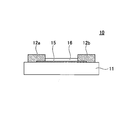
- FIG. 1A is a basic configuration diagram of a nanocarbon light source 10 used in the infrared analysis device of the embodiment.
- a nanocarbon material 15 is disposed on the substrate 11, and electrodes 12 a and 12 b are formed on both ends of the nanocarbon material 15.
- the electrodes 12 a and 12 b are electrically connected to the nanocarbon material 15 at both ends of the nanocarbon material 15.
- the nanocarbon light source 10 has a planar structure in which a nanocarbon material 15 as a light emitting layer is exposed on the surface. Since the electrodes 12 a and 12 b may be electrically connected to the nanocarbon material 15, some or all of them may be embedded in the substrate 11.
- the nanocarbon material 15 can be formed on any substrate such as a silicon substrate or a glass substrate, and the substrate 11 can be of any material or type such as a silicon substrate, a glass substrate, or a polymer substrate.
- the nanocarbon material 15 single-walled carbon nanotubes, multi-walled carbon nanotubes, single-layer graphene, multilayer graphene, thin graphite, or the like is used.
- the carbon nanotube may be a single carbon nanotube or a carbon nanotube thin film in which a plurality of carbon nanotubes are formed in a sheet shape. Since the nanocarbon light source 10 emits light if the nanocarbon material 15 can be energized, the electrical characteristics of the nanocarbon material 15 may be metallic or semiconducting.
- the nanocarbon material 15 may have a structure exposed on the substrate 11 as shown in FIG. 1A. However, as shown in FIG. 1B, the surface of the light-emitting element containing the nanocarbon material 15 is covered with a light-transmitting protective film 16. Also good.
- a protective film 16 an insulating thin film that is light transmissive with respect to the wavelength used may be used, such as silicon oxide or alumina.
- the nanocarbon light source 10 emits light by heating the nanocarbon material 15 through a pair of electrodes 12a and 12b. Due to the current heating, the temperature of the nanocarbon material 15 is increased, and light is emitted by heat radiation (called black body radiation or gray body radiation) accompanying the temperature increase.
- the thermal radiation from the nanocarbon light source 10 has an emission spectrum described by a black body radiation expression called Planck's law, and a broad emission spectrum mainly in the infrared region (far infrared to near infrared). have.
- Planck's law an emission spectrum described by a black body radiation expression called Planck's law, and a broad emission spectrum mainly in the infrared region (far infrared to near infrared). have.
- the temperature of the nanocarbon material 15 can be increased, and light can be emitted into the visible light region. it can.
- a new infrared analysis technique using the nanocarbon light source 10 as an infrared light source is realized.
- a halogen lamp or a ceramic light source is used as an infrared light source, but these light sources are large in the order of millimeters and have a slow response speed of about 100 ms. Therefore, there are problems that a spatial resolution of 10 ⁇ m or less cannot be obtained due to the diffraction limit of infrared light, high-speed measurement cannot be performed, and integration on a chip is not possible.
- the nanocarbon light source 10 of the embodiment behaves as an infrared light source by blackbody radiation, but unlike a conventional infrared light source, (i) ultra-small size of nanometer order is possible, (ii) silicon They can be integrated on any substrate such as a chip or glass, and (iii) can emit light at a high response speed of 100 ps.
- the nanocarbon light source 10 it is possible to realize a high-speed and high spatial resolution infrared spectroscopic analysis apparatus, and it is possible to develop an infrared spectroscopic apparatus based on a new principle that cannot be realized with a conventional infrared light source.
- FIG. 2 is a schematic diagram of a probe-type light source 20 including the nanocarbon light source 10.
- the nanocarbon light source 10 may be formed on a substrate having any shape.
- a light-emitting element formed on a flat substrate 11 as shown in FIGS. 1A and 1B may be used, and a nano-structure is formed at the tip of a convex substrate 11A processed into the shape of a protrusion or a probe as shown in FIG.
- the carbon light source 10 (or nanocarbon light emitting element) may be built in. Even if the shape of the substrate 11A is a probe type, the tip of the substrate 11A can be a flat surface, and the light emitting surface of the nanocarbon light source 10 (that is, the arrangement surface of the nanocarbon material) has a two-dimensional extent. It can also be a flat surface. Even when the tip of the substrate 11A is processed into a curved surface, the nanocarbon light source 10 can be produced on the curved surface.
- the measurement object is irradiated with infrared light in a state where the nanocarbon light source 10 is brought close to the measurement object. And can be measured.
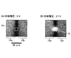
- FIG. 3 is an infrared camera image of the actually produced nanocarbon light source 10.
- Graphene is used as the nanocarbon material 15.
- FIG. 3A is an image of the element surface in a state in which the applied voltage is 0 V, that is, no voltage is applied to the electrodes 12a and 12b. A dark region between the pair of electrodes 12a and 12b is the graphene nanocarbon material 15.
- FIG. 3 shows the light emission state by voltage application.
- a voltage of 3.7 V is applied to the nanocarbon material 15, and it can be seen that the graphene (G) portion emits light.
- This light emission is infrared wavelength light and can be used as measurement light for irradiating the measurement object.
- FIG. 4 is a schematic diagram of the infrared analysis apparatus 100 of the first embodiment.
- the infrared analysis apparatus 100 includes a nanocarbon light source 10 and spectroscopes / photodetectors 110-1 and 110-2.
- a sample S to be measured is disposed between the nanocarbon light source 10 and the spectroscope / photodetectors 110-1 and 110-2.
- the spectroscope / photodetector 110-1 detects reflected light L R from the sample S, scattered light L S and the like.
- Spectroscope and photodetector 110-2 detects the transmitted light L T transmitted through the sample S.
- the spectroscope / photodetector 110 is not necessarily arranged on both the reflection side and the transmission side of the sample S, and may be arranged only on one side.
- a predetermined measurement region 101 on the sample S is irradiated with infrared light generated from the nanocarbon light source 10.
- Part of the infrared light L IR irradiated from the nanocarbon light source 10 is absorbed by the infrared absorption due to the molecular vibration of the sample S or the like.
- Infrared light accompanied by this absorption is observed by light transmitted, reflected, or scattered by the sample S.
- the light absorption in the sample S can be measured by observing at least one of the transmitted light L T , reflected light L R , and scattered light L S with the spectroscope / photodetector 110.
- the absorption spectrum can be measured by spectroscopy using a diffraction grating, a Michelson interference system, or the like.
- the sample S may be a solid, liquid, or gaseous substance, and the state of the sample S arranged between the nanocarbon light source 10 and the spectroscope / photodetector 110 is detected by the infrared analyzer 100. Can be analyzed. Since the nano-carbon light source 10 having a small planar light emitting structure is used, it is also possible to locally measure a part of the sample S by bringing the light source and the sample S close to each other. In particular, when the probe-type light source 20 as shown in FIG. 2 is used, local measurement can be performed by bringing the light source close to the sample surface regardless of the shape of the sample S.
- FIG. 5 is a diagram showing local infrared measurement using a near field.
- the nanocarbon light source 10 of the embodiment or the probe-type light source 20 using the nanocarbon light source 10 has a planar structure in which the light source itself is a minute size and the light emitting layer can be exposed. Using this nano-carbon unique light emitting structure, high spatial resolution local region measurement is realized by the near field generated in the vicinity of the nano-carbon light source 10.
- the light generated from the nanocarbon light source 10 is not only extracted by a remote field and used for measurement, but also can be measured by a near field generated in the vicinity of the light source.
- This near field is exponentially attenuated depending on the distance from the light source, and is a field that exists only in the vicinity of the light source.
- the near-field light 102 can be taken out by bringing the sample S to be measured close to the nanocarbon light source 10 and can be used for measurement.
- Near-field light 102 is local light that is determined by the size of the light source regardless of the diffraction limit, unlike normal far-field light. Therefore, it is possible to perform ultra-high spatial resolution local infrared measurement beyond the diffraction limit which is a problem in conventional infrared spectroscopy.
- the size of the nanocarbon light source 10 can be reduced to the order of nanometers, it is possible to measure a small area with a difference of 10 ⁇ m, which is the diffraction limit in the conventional infrared spectroscopy.
- the near-field generated by the nanocarbon light source 10 of the embodiment differs from the near-field light generated locally in the fine pores and the spherical surface at the tip of the sharp probe probe, and is generated in the vicinity of the light source itself. Field, which is completely different in principle from conventional near-field spectroscopy.
- a conventional near field using a pore or a probe tip is generated electromagnetically at the pore or the probe tip by irradiating laser light or the like to the pore or the probe tip from the outside.
- the near field of the embodiment uses a near field generated in the fine nanocarbon light source 10 itself, and a “near field generated in the vicinity of the light source” is used without using an external laser beam or the like as in the prior art. This is a near-field infrared measurement based on a new principle.
- the light emitting region has a planar structure that can be exposed to the outside” It cannot be realized unless it is an element having a planar structure in which the light emitting layer is exposed, such as the nanocarbon light source 10 of the embodiment.
- the metal filament used as the light emitting layer has a large size on the order of millimeters, and the filament portion is sealed with a glass tube or the like so that the light emitting layer is brought closer to the sample to be measured. I can't.
- the nanocarbon light source 10 is an element having a planar structure in which the nanocarbon of the light emitting layer is exposed, in addition to being a minute light source that can be reduced to the nanometer order at the minimum. The sample S can be made very close.
- the intensity of near-field light decreases exponentially with respect to the distance from the light emitting layer, it is necessary to bring the light emitting layer and the sample S to be measured sufficiently closer than the wavelength. In order to use the near field in the vicinity of the light source, it cannot be realized unless the light source has a planar structure such as the nanocarbon light source 10. Further, since the infrared analyzer 100 uses the near field of the minute nanocarbon light source 10 itself, it is not necessary to use an expensive and large laser light source, and the ultra-small infrared analyzer 100 can be realized at low cost.
- the nanocarbon light source 10 may have a configuration in which the nanocarbon material 15 is completely exposed as shown in FIG. 1A, or the nanocarbon material 15 may be covered with a thin protective film 16 as shown in FIG. 1B. If the protective film 16 is thin, a near field can be used. Usually, there is no problem if the thickness of the protective film 16 is smaller than the wavelength of light, and the intensity of near-field light increases as the film thickness decreases.
- the nanocarbon light source 10 is capable of extremely fast infrared emission with a response time of the order of 100 ps, unlike an infrared light source such as a conventional halogen lamp.
- a modulated voltage or current such as a pulse or a rectangle
- a short pulse light of the order of 100 ps or a rectangular light emission with a quick rise can be obtained.
- infrared light with free intensity modulation can be obtained.
- a pulse laser is currently used, and time-resolved spectroscopic measurement using a short pulse light source of femto to nanosecond is performed.
- a short-pulse laser light source is currently used in the ultraviolet, visible, and near-infrared regions, but there is no high-speed pulsed laser light source in the mid-infrared region.
- the laser light source is a light source having a very narrow wavelength width, it does not have a broad emission spectrum necessary for infrared spectroscopy or the like.
- the nanocarbon light source 10 of the embodiment is a very high-speed light source as described above, the emission spectrum is in the infrared to visible region described by the Planck rule of blackbody irradiation. It has a very broad spectrum. Therefore, not only can it be used for infrared spectroscopy as in the case of a conventional halogen lamp, but also time-resolved infrared measurement with a very high time resolution on the order of 100 ps, which is impossible with a halogen lamp, becomes possible.
- Such an ultrafast infrared analyzer does not exist in the current technology, and the infrared analyzer 100 of the embodiment is an infrared analyzer based on a new principle.
- the infrared analysis apparatus 100 of the embodiment can also perform infrared sensing using infrared spectroscopy.
- spectroscopic analysis in order to analyze a general material, spectrum measurement is performed by a spectroscope or the like. However, the spectroscope becomes a large device and is expensive.
- the presence or absence, concentration, amount, and mixing of a specific solid / liquid / gas substance can be detected by limiting the detection to infrared light in a specific wavelength range with a filter or the like without using a spectroscope. Sensing the ratio and so on.
- the ultra-small structure using the nanocarbon light source 10 enables sensing of various substances, and a small sensor can be manufactured.
- measurement is performed by bringing the nanocarbon light source 10 close to the sample S to be measured, or sensing solid, liquid, or gaseous substances existing in the space between the nanocarbon light source 10 and the spectroscope / photodetector 110. It is possible.
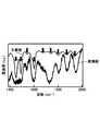
- FIG. 6 shows an example of infrared spectroscopy using the nanocarbon light source 10 using graphene. It is the example which carried out the infrared transmission light measurement of the polystyrene by the system of FIG. 5 using the nano carbon light source 10 which has a graphene of 500 micrometers square.
- the lower spectrum in the figure is an actually measured value in the infrared analyzer 100 using the nanocarbon light source 10, and the upper spectrum is a literature value.
- the absorption peak of the spectrum matches the literature value, and the infrared analysis apparatus 100 of the embodiment can obtain the same result as the conventional infrared spectroscopic analysis by FT-IR.
- This measurement result shows that infrared spectroscopic analysis such as vibrational spectroscopy using the nanocarbon light source 10 is actually possible.
- the nanocarbon light source 10 of the embodiment can directly modulate the emission intensity by applying a modulated voltage or current. Since the nanocarbon light source 10 itself can perform a high-speed blinking operation, high sensitivity measurement using direct intensity modulation of a light source that is difficult with a conventional infrared light source is possible. For example, by directly modulating the intensity of light emitted from the nanocarbon light source 10 and receiving it with a photodetector in synchronization with the modulated light, highly sensitive light detection is realized by synchronous measurement such as a lock-in amplifier and gate operation. Compared with the analysis with a conventional infrared light source, it is possible to perform spectroscopy / analysis / sensing with an infrared light source with extremely high sensitivity.
- time-resolved measurement is possible even if the detector side is a low-speed detector. Since a low-speed and high-sensitivity infrared detector can be used, time-resolved measurement can be performed with high sensitivity regardless of the type of infrared detector.
- FIG. 7A shows an example of direct intensity modulation using the nanocarbon light source 10. This is an example in which direct intensity modulation at 1 kHz is performed with the nanocarbon light source 10 using a 3 ⁇ m square graphene film.
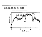
- FIG. 7B is an infrared spectroscopic analysis result of atmospheric molecules using directly modulated light from the nanocarbon light source 10 directly modulated at 163 Hz and an infrared detector using a lock-in amplifier. Carbon dioxide and water molecules in the atmosphere are detected in a broad wavelength range. The reason why absorption peaks are detected in different wavelength ranges for water molecules and carbon dioxide is that the types of molecular vibrations are different.
- continuous pulsed light is generated not only by single pulsed light by applying a single pulse electric signal but also by repeatedly applying a pulse voltage. Can do. Since it can be directly modulated at a very high speed, the timing of the generated pulsed light can be freely controlled. Using these characteristics, high-speed infrared analysis can be performed when a single pulsed light is generated at a certain timing. In addition, time-resolved measurement can be performed by inputting repeated pulsed light. In infrared analysis using repetitive pulsed light, time-resolved measurement can be performed by giving a delay time to the generation of pulsed light, thereby enabling strobe time-resolved infrared analysis.
- the nanocarbon light source 10 capable of broad spectrum and high-speed modulation
- a new analysis method can be realized by the infrared analyzer 100.
- FIG. 8 is a schematic diagram of a scanning infrared analyzer 100A of the second embodiment.
- infrared imaging is realized by scanning the nanocarbon light source 10 relative to the sample S.
- the infrared analysis apparatus 100A includes a probe-type light source 20 having a nanocarbon light source 10 at the tip, and spectrometers / photodetectors 110-1 and 110-2.
- the planar nanocarbon light source 10 is provided at the tip of the substrate 11A processed into a probe shape.
- the sample S to be measured is placed on a light-transmitting stage 22 such as glass, and is scanned while irradiating the sample S with light from the light source 20.
- a light-transmitting stage 22 such as glass
- At least one of the probe-type light source 20 and the stage 22 is connected to a three-axis manipulator (not shown) and can move in the three-axis direction. Thereby, one of the nanocarbon light source 10 and the sample S scans relative to the other.
- the detection signal can be converted into an image signal and used as an infrared imaging apparatus.
- the nanocarbon light source 10 is a very small infrared light source and has a planar structure in which the light emitting layer can be exposed on the surface.
- a one-dimensional, two-dimensional, or three-dimensional infrared is obtained by scanning the nanocarbon light source 10 one-dimensionally, two-dimensionally, or three-dimensionally with the light-emitting layer approaching or contacting the sample S to be measured. Imaging becomes possible. For example, changes in the intensity and spectrum of transmitted / scattered / reflected light are caused by infrared absorption due to molecular vibrations in the sample S, etc., so changes in one, two, or three dimensions are observed as images. can do. Since transmitted / scattered / reflected light can be dispersed by a spectroscope, imaging depending on wavelength is also possible.
- the infrared analyzer 100A is suitable not only for imaging but also for analysis in a specific local region.
- the probe-type light source 20 is fixed to a location where the sample S is present, and infrared spectroscopy of the minute region is possible.
- the nanocarbon light source 10 is brought close to the sample S to a distance equal to or shorter than the wavelength, and measurement using near-field light is performed. Is possible. That is, imaging with high spatial resolution and spectral imaging are possible beyond the diffraction limit of light.
- the conventional micro-infrared spectroscopy analyzer can improve the spatial resolution, which is about 10 ⁇ m at the diffraction limit, to the nanometer order in the near field.
- the sample S to be measured objects of any shape can be imaged, and in addition to normal liquids and solids, it can also be used for bioimaging of biological tissues such as cells. In the chemical, bio, material, and physical fields Imaging is possible.
- FIG. 9 shows the results of infrared imaging measurement using the infrared analyzer 100A.
- the sample S on which the number “5” arranged on the glass is patterned is scanned. It can be seen that an infrared image reflecting the shape of the sample S is obtained.
- FIG. 10 is a schematic diagram of an infrared analyzer 100B of the third embodiment.
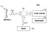
- the infrared analysis apparatus 100B includes a nanocarbon light source 10, an excitation source 105, and a spectrometer / photodetector 110.
- the nanocarbon light source 10 is used as a probe light source, and outputs an infrared probe light L probe .
- the output of the spectroscope / photodetector 110 may be connected to the input of the information processing apparatus 103.
- a conventional light source having only a low response speed (about 100 ms) such as a halogen lamp or a ceramic light source cannot perform high-speed infrared spectroscopic analysis or high-speed time-resolved measurement by modulating the light source. For example, chemical reactions that change from moment to moment cannot be traced by infrared spectroscopy.
- the nanocarbon light source 10 since the nanocarbon light source 10 has a very fast light emission response speed of the order of 100 ps, the nanocarbon light source 10 is used as the light source, so that the infrared analysis apparatus 100B has an ultrafast speed of 100 ps. Time resolution can be provided.
- the infrared analysis apparatus 100B can track high-speed chemical reactions and the like by infrared spectroscopy. As described above, when the light source side is high speed, the detector side can perform time-resolved measurement with any low-speed detector. Therefore, an ultrasensitive photodetector can be used as the spectroscope / photodetector 110.
- a chemical reaction pulse stimulus P for starting a chemical reaction is applied to the measurement region 101 of the sample S from an excitation source 105 such as a pump light source.
- the measurement region 101 is irradiated with a pulse of the probe light L probe from the nanocarbon light source 10 with a delay time of ⁇ t seconds from the irradiation of the pump light.
- the chemical reaction pulse is not limited to light irradiation, and an electrical stimulation or substance supply such as application of an electrochemical reaction voltage or supply of a reactant pulse is performed. May be.
- the photochemical reaction can be started by irradiating the sample to be measured with light.
- an electrode for causing an electrochemical reaction is formed in the sample to be measured, and an electrical signal such as a reaction start voltage is input to this electrode.
- the reaction is started by mixing or the like by supplying a substance necessary for a chemical reaction from a flow path or the like.
- These chemical reaction pulse stimulations may be the waveform stimulation shown in FIG. 10 or a rectangular stimulation supply.
- Changes in the sample caused by stimulation are detected by the spectroscope / photodetector 110 as transmitted light, scattered light, or reflected light.
- the detected light may be input to the information processing apparatus 103 as a result of infrared absorption by excited molecular vibration, for example, and signal processing, analysis, or the like may be performed.
- the information processing apparatus 103 may have a digital signal processing function such as a spectrum analyzer or an image signal converter.
- FIG. 11 shows an example of a change in the measurement substance due to chemical reaction stimulation.
- the chemical reaction pulse stimulus is applied to the sample in the measurement system of FIG. 10, the chemical reaction proceeds by the chemical reaction stimulus as shown in FIG. 11, and the final product is obtained through the reaction process and the intermediate. It is done.
- the sample S is irradiated with infrared light from the nanocarbon light source 10 as the probe light L probe after a delay time ⁇ t seconds from the application timing t1 of the chemical reaction pulse stimulation (L pump ), the reaction process and the intermediate production state
- the sample S is irradiated with infrared light.
- the spectroscope / photodetector 110 By measuring the transmitted / scattered / reflected light from the sample S with the spectroscope / photodetector 110, it becomes possible to analyze the reaction process, the vibration spectroscopy of the intermediate, and the like.
- the infrared analysis depending on the time of the sample S is possible.
- a spectroscope in such a measurement system a spectroscope using a grating or Michelson interference can be used.
- time-resolved measurement by a step-and-scan method using a high-speed light source is also possible.
- high-speed time-resolved measurement is realized on the side of the infrared light source (nanocarbon light source 10), so there is no need to use a high-speed photodetector for the time resolution of infrared spectroscopy, A photodetector may be used.
- high-speed photodetectors have poor light receiving sensitivity, and high-sensitivity photodetectors are slow, so sensitivity and speed were a trade-off, but they could not be used conventionally due to the configuration and method of the embodiment.
- High-speed time resolution using a highly sensitive photodetector can be realized.
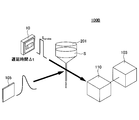
- FIG. 12 shows an example of a measurement system using chemical reaction pulse stimulation and repeated irradiation of probe light.
- a gas, liquid, or solid sample is placed in the measurement region 101.
- the sample S can be supplied by the flow cell 201 or the like.
- infrared light (L probe ) from the nanocarbon light source 10 is irradiated with a delay time ⁇ t, and this is repeated.
- the infrared light from the carbon light source 10 is, for example, ultrashort pulse infrared light.
- the response by pulse stimulation and the measurement by infrared light are repeatedly measured at high speed and integrated by the spectroscope / photodetector 110 or the information processing apparatus 103, so that the S / N ratio is increased by the amount corresponding to the number of repetitions. Sensitivity can be measured.
- any stimulus that initiates a chemical reaction such as photochemical reaction excitation light, electrochemical reaction voltage, and reactant pulse supply, can be applied.
- There are various methods for applying the stimulus and by performing measurement by changing the delay time ⁇ t little by little, it is possible to analyze the reaction process that progresses from moment to moment.
- a grading or Michelson interferometer can be used as a spectrometer, and a step-and-scan method can also be used. Since the photodetector can use a low-speed and high-sensitivity photodetector, high-sensitivity measurement is possible.
- the high-speed time-resolved measurement by the infrared analyzer 100B of the third embodiment involves precise delay time control, but can be realized because the nanocarbon light source 10 can generate ultrashort-pulse infrared light at an arbitrary timing. It is.
- the nano carbon light source 10 is used to the maximum extent that it is a high-speed light source that can be directly modulated.
- FIG. 13 is a diagram showing short pulse emission from the nanocarbon light source 10.
- the time resolution of the infrared analyzer 100B is determined by the response speed of light emission of the nanocarbon light source 10.
- the nanocarbon light source 10 high-speed time-resolved measurement using short-pulse light of the order of 100 ps is realized as shown in FIG.
- FIG. 14 is a schematic diagram of an infrared analyzer 100C according to the fourth embodiment.
- infrared measurement using a microanalysis chip having a microchannel is realized.
- the micro analysis chip is an example of an infrared analysis chip that efficiently performs infrared spectroscopy (or absorption) analysis.
- the infrared analysis apparatus 100C includes a nanocarbon light source 10 and a spectroscope / photodetector 110.
- a micro analysis chip 108 may be arranged between the nanocarbon light source 10 and the spectroscope / photodetector 110.
- a micro flow path 107 is formed in the micro analysis chip 108, and the sample S is supplied into the micro flow path 107.
- the microanalysis chip 108 having the microchannel 107 is effectively used for a small amount of chemical analysis, bioanalysis, medical diagnosis and the like.
- the nanocarbon light source 10 can be formed of any inorganic or organic material including silicon, glass, polymers, and the like.
- the light emitting layer has a planar structure that can be exposed.
- Nanocarbon light source 10 is positionable adjacent to the microchannel 107 of the micro analysis chip 108, it can be realized measurement and analysis on the chip using infrared light L IR from nanocarbon light source 10.
- the micro analysis chip 108 can produce a chip body having the micro flow path 107 by using an inorganic material such as silicon or glass, or an organic material such as a polymer.
- the nanocarbon light source 10 is disposed in the vicinity of (for example, directly below) the microchannel 107. Infrared light from the nanocarbon light source 10 is applied to the sample S flowing through the microchannel 107, and transmitted / scattered / reflected light (Lout) from the sample S is observed by the spectroscope / photodetector 110. Thereby, infrared analysis or sensing of the substance flowing through the micro flow path 107 becomes possible.
- the nanocarbon light source 10 may be disposed outside the microanalysis chip 108 by bonding or the like so as to face the microchannel 107.
- the nanocarbon light source 10 is a light source having a fine and planar structure, and can be directly formed on various substrates. Therefore, the nanocarbon light source 10 can be directly formed on the microanalysis chip 108 in which the microchannel 107 is formed or directly in the microchannel 107.
- the carbon light source 10 may be formed.
- the third embodiment is achieved by forming the microchannel 107 capable of inputting chemical reaction pulse stimulation such as photochemical reaction excitation light, electrochemical reaction voltage, and reactant pulse supply.
- chemical reaction pulse stimulation such as photochemical reaction excitation light, electrochemical reaction voltage, and reactant pulse supply.
- the time-resolved measurement similar to the form becomes possible.
- the microchannel 107 is irradiated with pump light for photochemical reaction from the outside, and an electrode for electrochemical reaction is formed in the microchannel 107 to apply electrical stimulation. .
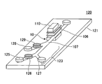
- FIG. 15 is a schematic diagram of a micro analysis chip 120 in which the nanocarbon light source 10 and the detector are integrated on a substrate.
- a spectroscope / photodetector 110 and an optical filter 106 such as a band pass filter may be further integrated on the micro analysis chip 120 having the nanocarbon light source 10.
- This integrated configuration realizes a complete on-chip micro analysis chip 120 in which all optical components are integrated on the chip without using an external spectroscope or photodetector.
- the microchannel 107 is formed above the nanocarbon light source 10 in the stacking direction, and the spectroscope / photodetector 110 is disposed further above the microchannel 107, thereby The reaction (infrared absorption etc.) by the infrared light and the sample in the microchannel 107 can be directly measured.
- the micro analysis chip 120 having the micro flow channel 107 is also an example of an infrared analysis chip.
- the microchannel / reactor 123 may be configured by branching the microchannel 107 and providing the supply nozzles 125 to 129 in the branch channel.
- the A fluid is supplied from the supply nozzles 125 and 128, the B fluid is supplied from the supply nozzles 126 and 129, and the C fluid is supplied from the supply nozzle 127.
- the mixed fluid flows over the nanocarbon light source 10 by the merge of the flow paths.
- the optical filter 106 By forming the optical filter 106 above or below the microchannel 107, only a specific wavelength can be detected for analysis, sensing, and the like.
- a single-element photodetector can be used as the spectroscope / photodetector 110, but an array-shaped photodetector may be used.
- spectroscopic measurement can also be performed on the chip by arranging optical filters having different center wavelengths in an array.
- the nanocarbon light source 10 is very small and highly integrated, it can be easily arrayed.
- the nanocarbon light source 10 is arrayed, it is possible to perform spectroscopy even if the spectroscope / photodetector 110 is a single element.
- the optical filters 106 having different center wavelengths may be arranged in an array so as to face the nanocarbon light source 10 formed in an array. By controlling the lighting timing of each of the nanocarbon light sources 10 arranged in an array, it is possible to perform spectroscopy using a single-element spectroscope / photodetector 110.
- the time-resolved measurement by the chemical reaction pulse stimulation of the third embodiment can also be applied to the micro analysis chip 120 of FIG. In this case, a highly integrated time-resolved measurement chip is realized.
- FIG. 16 is a diagram for explaining the principle of infrared analysis according to the fifth embodiment.
- an infrared analysis technique using a biochip in which a probe substance is fixed to a minute infrared light source such as the nanocarbon light source 10 is provided.
- the biochip used here is also an example of an infrared analysis chip.
- a sample for analysis is supplied onto a biochip, and the sample substance is bound to a probe substance fixed to a fine infrared light source to perform infrared analysis simply and at high speed.
- a biochip as an application of semiconductor microfabrication technology to the bio field.
- one or a plurality of fixed probes (DNA, proteins, sugar chains, cells, molecules, etc.) are arranged on the surface of a substrate such as a semiconductor / insulator.
- the fixed probes may be arranged in a one-dimensional or two-dimensional array.
- the analysis is performed by utilizing the property that the sample substance (DNA, protein, sugar chain, cell, molecule, etc.) selectively binds to the fixed probe on the substrate.
- a “phosphor” is attached to a fragment of an analysis sample material, and the fluorescence pattern is analyzed to detect and analyze the sample material.
- Phosphors are extremely expensive, and the analysis apparatus itself is large, so that it is an extremely expensive analysis technique.
- a minute infrared light source for example, a nanocarbon light source
- a fixed probe is disposed on the minute infrared light source.
- the analysis sample material selectively bonded to the fixed probe is identified, detected, and analyzed using infrared absorption of light output from a micro infrared light source.
- a stationary probe 131 for analysis is placed on a minute infrared light source such as the nanocarbon light source 10 formed on the substrate 11 to produce a light source integrated biochip 130.
- a minute infrared light source such as the nanocarbon light source 10 formed on the substrate 11 to produce a light source integrated biochip 130.
- DAN DAN, protein, sugar chain, cell, molecule or the like can be used.
- the fixed probe 131 selectively binds to a specific sample substance (DNA, protein, sugar chain, cell, molecule, etc.).
- the fixed probe 131 can be formed by directly coupling to the nanocarbon light source 10 constituting the minute infrared light source, or a cap layer is provided on the nanocarbon light source 10 and the fixed probe is coupled to the cap layer. May be.
- a sample substance 135 that can be selectively combined with the fixed probe 131 is bonded to the fixed probe 131. Since the binding between the fixed probe 131 and the sample material 135 is selective, the fixed probe 131 can be selected so that only a specific sample material 135 is bonded to the fixed probe 131. Using this property, it is possible to identify, detect, and analyze (specify molecular structure, etc.) sample materials for analysis.
- the analysis sample immediately above the micro-infrared light source and marker molecules modified to the analysis sample cause infrared absorption. Identify, detect, or analyze analytical samples by infrared absorption due to molecular vibrations inside the sample by measuring the spectrum and transmittance of infrared light that has passed through the analytical sample captured on a micro-infrared light source be able to.
- the technique of the fifth embodiment eliminates the need for a fluorescent marker required for conventional biochip analysis.
- the sample material 135 itself for analysis or the molecule itself modified to the sample material 135 serves as a marker, and utilizes infrared absorption such as molecular vibration.
- infrared absorption such as molecular vibration.
- fluorescent markers that emit light in the visible region
- absorption in the infrared region by molecules is used, so non-luminescent molecules that could not be used as markers in the conventional method can also be used as markers for biochip analysis. Realize low-cost biochip analysis.
- the micro light source may be a compound semiconductor light emitting element operating in the infrared region or an organic light emitting element.
- the nanocarbon light source 10 is used as a minute light source, light can be emitted in the visible light region, and thus a biochip 130 using absorption of visible light can be developed. Further, it is possible to perform analysis using a conventional phosphor using visible light from the nanocarbon light source 10 as excitation light.
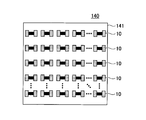
- FIG. 17 is a schematic diagram of an infrared light source array 140 applied to the biochip 130 of the embodiment.
- a high-capacity analysis can be performed at a higher speed by arranging micro infrared light sources in a one-dimensional or two-dimensional array.
- a large number of nanocarbon light sources 10 are arranged on a substrate 141 in a two-dimensional array.
- the infrared light source array 140 can be easily obtained at low cost because the light source is fine and easy to manufacture.
- each of the nanocarbon light sources 10 has high-speed light emission responsiveness, the nanocarbon light sources 10 arranged in an array can be independently controlled at high speeds at different timings.
- FIG. 18A shows an infrared light source array 140A using a matrix electrode as a modification.
- FIG. 18B is a circuit diagram of an infrared light source array having a rectifying action.
- a plurality of electrodes 142 extending in the horizontal direction and a plurality of electrodes 143 extending in the vertical direction are electrically insulated from each other and arranged to cross each other.
- the horizontal electrode 142 has comb-like electrode protrusions 142t. Each electrode protrusion 142t is opposed to the vertical electrode 143 to form an electrode pair.
- a carbon nanomaterial is connected to each electrode pair to constitute one nanocarbon light source 10 cell.
- each cell may be given a rectifying effect.
- a rectifying element (for example, a diode) 145 is connected in series with the resistive nanocarbon light source 10.
- the element 145 suppresses a path due to the backflow of current, and makes it easy for only the nanocarbon light source 10 at a desired position to emit light.
- a high potential is applied to the selected horizontal electrode 142 and the other electrodes 142 are turned OFF.
- a low potential is applied to the selected vertical electrode 143, and the other electrodes 143 are turned OFF.
- the nanocarbon light source 10 at a position determined by the selected electrode 142 and electrode 143 emits light. In this configuration, since a current that bypasses the light source other than the selected light source is suppressed, it is possible to increase the light emission efficiency and to suppress malfunction (mislight emission) of other light sources.
- FIG. 19 is a schematic diagram of an infrared analyzer 160 according to the fifth embodiment.
- the infrared analyzer 160 includes a biochip 150 integrated with an infrared light source array 140 (or 140A), and a spectrometer / photodetector 110.
- the biochip 150 is also an example of an infrared analysis chip.
- a condensing lens 151 may be disposed between the biochip 150 and the spectroscope / photodetector 110.
- each of the nanocarbon light sources 10 arranged in a one-dimensional or two-dimensional array has a fixed probe 131 as shown in FIG. Is formed.
- the sample material 135 to be analyzed is bound to the fixed probe 131, the infrared light 155 from the nanocarbon light source 10 is absorbed, and analysis based on infrared absorption becomes possible.
- FIG. 19 even when a single spectroscope / photodetector 110 is used, two-dimensional chip analysis is possible by controlling the timing of light emission of each nanocarbon light source 10 and synchronizing it with the detection timing. is there. For example, as shown by the arrows in FIG. 19, information on each cell can be obtained by the spectroscope / photodetector 110 by sequentially scanning and turning on the arrayed nanocarbon light sources 10.
- a plurality of types of fixed probes 131 necessary for analysis may be formed on each nanocarbon light source 10 of the biochip 150.
- different types of sample substances 135 can be simultaneously detected and analyzed corresponding to the different types of fixed probes 131.
- An analysis sample material to be analyzed is introduced onto the biochip 150 and brought into contact with a plurality of types of fixed probes 131.
- the sample substance 135 is bound to one type of fixed probe 131, but the sample substance 135 is bound to another type of fixed probe 131. Do not combine.
- the arrayed nanocarbon light sources 10 emit light sequentially, and the spectroscope / photodetector 110 detects the infrared light 155 in synchronization with the light emission, so that the sample substance 135 is bound to the specific fixed probe 131. It can be detected whether or not.
- the sample substance 135 itself or a molecule modified to the sample substance 135 causes infrared absorption due to molecular vibration or the like based on the same principle as described with reference to FIG.
- the sample substance 135 can be identified, detected, and analyzed.
- An expensive fluorescent marker is unnecessary, and non-luminescent molecules that could not be used as a marker in the conventional method can also be used as a marker for biochip analysis.
- the nanocarbon light sources 10 are arranged in an array, analysis using various types of fixed probes 131 can be performed on the same biochip 150 at the same time.
- the biochip 150 is inexpensive, enables high speed and large capacity analysis.
- very minute light sources can be arrayed in one or two dimensions.
- each nanocarbon light source 10 can be individually controlled to be turned on at a high speed at different timings.
- various types of fixed probes 131 can be patterned in any arrangement.
- the array pattern of infrared absorption and infrared spectrum obtained by analysis is a pattern reflecting the molecular structure and properties of the substance in biochip analysis.
- the infrared light source side using the nanocarbon light source 10 is a two-dimensional array, and each nanocarbon light source 10 can be controlled to be lighted independently.
- a single channel spectroscope / photodetector 110 can be used by emitting the arranged nanocarbon light sources 10 in order.
- the configuration of the infrared analysis device 160 is simplified, and the device can be configured at low cost.
- Infrared light detectors do not have high-performance two-dimensional detectors compared to visible detectors. Since the high-performance infrared detector becomes a single-channel detector, the technique of the embodiment enables the use of a high-performance single-channel photodetector. By controlling the emission timing of the nanocarbon light source 10, spectroscopy is facilitated, and biochip analysis using spectroscopy is also possible. In addition, since the nanocarbon light source 10 can emit light even with visible light, a biochip utilizing analysis or absorption of visible light using a conventional phosphor can be developed.
- This biochip analysis technique can also be combined with the configurations and methods of the first to fourth embodiments.
- FIG. 20 is a diagram illustrating an application of the sixth embodiment to an imaging device.
- an array arrangement of fine infrared light emitting elements such as the nanocarbon light source 10 is applied to infrared imaging.
- the infrared imaging device includes an infrared light source array 140 in which a plurality of infrared light emitting elements are arranged, and a spectroscope / photodetector 110 (see FIG. 19 and the like) disposed to face the infrared light source array 140.
- a spectroscope / photodetector 110 see FIG. 19 and the like
- the nanocarbon light source 10 may be used. Unlike conventional infrared light sources such as halogen lamps, the nanocarbon light source 10 can be integrated on a variety of substrate materials including silicon, glass, semiconductors, insulators, polymer substrates, and individual light sources. The element can be turned on independently.
- the sample S includes a bio sample, a biological sample, an organic material, an inorganic material, and the like.
- Imaging the infrared absorptivity and spectrum on each light source by synchronizing the lighting timing of each light emitting element included in the infrared light source array 140, for example, the nanocarbon light source 10, and the detection timing of the spectroscope / photodetector. Can be performed at high speed. In addition, since a single detector is sufficient, wavelength selection combined with a spectroscope and a filter is easy, and spectral imaging for imaging for each wavelength can be easily realized.
- This infrared imaging can be realized by utilizing the characteristics of the nanocarbon light source 10 such as “high-speed light source” and “micro light source”, and cannot be realized by conventional infrared analysis technology using a halogen lamp or a ceramic light source. This is a new imaging technique.
- infrared imaging may be performed using an element capable of high-speed response and miniaturization, such as a semiconductor light emitting element or an organic light emitting element.
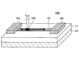
- FIG. 21 is a schematic diagram of a nanocarbon light source 10A of the seventh embodiment.
- the nanocarbon light source 10A includes a nanocarbon material 15 and a gate electrode 19 that extend in a predetermined direction between a pair of electrodes 12a and 12b.
- the nanocarbon material 15 extending long in the predetermined direction is, for example, one or more layers of graphene.
- Graphene may be grown directly on the substrate 11 by CVD or the like, or may be formed by transfer or the like.
- the gate electrode 19 not only a metal electrode such as a metal material but also a conductive substrate itself such as doped silicon can be used as an electrode.
- the gate electrode 19 may be formed of a conductive transparent material on the back surface of the substrate 11 (the surface opposite to the nanocarbon material 15).
- the gate electrode may be an electrode widely formed under the substrate, or may be a gate electrode locally formed only directly under the graphene.
- the substrate 11 on the gate electrode may be an insulator, and may be an insulating thin film material such as a silicon oxide thin film on silicon as well as the insulating substrate.
- the carrier concentration in the nanocarbon material 15 can be spatially controlled.
- a hot spot 109 that emits light brightly at a low carrier concentration can be formed. Light emission from the hot spot 109 is indicated by “L emit ” in the drawing.
- the position of the hot spot 109 can be continuously changed along the length direction of the nanocarbon material 15 by changing the voltage applied to the gate electrode.
- the nanocarbon light source 10 ⁇ / b> A capable of sweeping the light emission position in the length direction of the nanocarbon material 15 by the gate voltage can be manufactured.
- a single nanocarbon light source 10A element can be used to provide spatial resolution in a one-dimensional direction.
- This light source can be used as a light source for a one-dimensional imaging device.
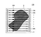
- FIG. 22 shows an infrared light source array 170 in which a plurality of nanocarbon light sources 10A of FIG. 21 are arranged in a direction orthogonal to the sweep direction.
- a two-dimensional imaging device can be realized by combining this infrared light source array 170 with a spectroscope / photodetector 110 and a gate voltage controller.
- the sample S can be directly mounted on the surface of the infrared light source array 170.
- One common gate electrode 19 may be formed on the back surface of the substrate 11, or a stripe-shaped gate electrode 19 may be provided for each corresponding nanocarbon light source 10A.
- the pair of electrodes 12a and 12b are sequentially selected, and the gate voltage is changed for each selected nanocarbon light source 10A, whereby a hot spot 109 is formed in the length direction of the nanocarbon material 15. Can be swept.
- the stripe-shaped individual gate electrodes 19 are used, the hot spots 109 can be simultaneously swept by the plurality of nanocarbon light sources 10A. In this case, high-speed imaging becomes possible.
- the length of the nanocarbon material 15 may be limited or the sweep distance of the hot spot 109 may be limited, but by arranging the nanocarbon light sources 10A in a two-dimensional plane. Wide-range and high-speed imaging becomes possible.
- the nanocarbon light sources 10A are arranged only in the vertical direction of the paper surface. However, a plurality of nanocarbon light sources 10 are also arranged in the horizontal direction (horizontal direction) of the paper surface through, for example, an insulating layer. A light source array may be used.
- FIG. 23 is a schematic configuration diagram of an imaging device 180 according to the seventh embodiment.
- the imaging device 180 includes an infrared light source array 170, a voltage control unit 210 that controls a voltage applied to the infrared light source array 170, and a spectroscope / light that detects infrared light (L emit ) transmitted through the sample S. It has a detector 110.
- a condensing lens 151 may be disposed between the infrared light source array 170 and the spectroscope / photodetector 110.
- An information processing device 103 including a display device may be connected to the output of the spectroscope / photodetector 110.
- the voltage control unit 210 controls the voltage level applied to the gate electrode 19.
- a plurality of arranged nanocarbon light sources 10A may be sequentially selected to control on / off of a voltage applied between the pair of electrodes 12a and 12b.
- the infrared spectroscopy of the present invention uses a minute infrared light source such as the nanocarbon light source 10.
- the light source element size can be reduced to 1 nm square, and when graphene is used, the size can be reduced to 100 nm square.
- a laser light source used in a conventional scanning near field optical microscope (SNOM) has a size of about 10 cm square at a minimum.
- Halogen lamps and ceramic light sources used in FT-IR are also about 1 cm square.
- the present invention since a minute infrared light source element is used, integration (chip formation) and array formation are possible, but a light source used in FT-IR or SNOM cannot be integrated or chipped. Further, according to the present invention, high sensitivity by modulation, analysis chip formation, and high-speed imaging using a two-dimensional array light source are possible, but neither of these effects can be obtained with either SNOM or FT-IR.
- the infrared analysis of the present invention measures over a wide wavelength range of 1 to 10 ⁇ m.
- FT-IR measures in the same wavelength range, but SNOM has a single wavelength of the laser or a narrow wavelength range.
- the spatial resolution As for the spatial resolution, a high spatial resolution of 1 nm to 100 nm is realized in the infrared analysis of the present invention.
- the spatial resolution of SNOM is as high as 10 nm, but 10 ⁇ m in FT-IR.
- Time resolution can be measured at a high speed of 100 ps in the infrared analysis of the present invention, but a typical FT-IR is slow at 100 ms. In SNOM, time-resolved measurement is usually difficult.
- a small light source size has high spatial resolution and temporal resolution, and integration, high sensitivity by modulation, analysis chip formation, and high-speed imaging are possible.
- the structure and method of invention were demonstrated based on specific embodiment, this invention is not limited to the specific example mentioned above.
- the first to seventh embodiments may be combined with each other.
- the biochip 130 and / or 150 of the fifth embodiment and the infrared imaging of the sixth embodiment can both be realized with a two-dimensional infrared array light source, red using the biochip 130 or 150 is used. Outside imaging is possible.
- a nanocarbon light source is one of the ideal candidates.
- An external light source may be used.
- biochips using visible light and fluorescent markers have been put to practical use as biochips such as DNA chips, but expensive fluorescent markers and cameras with two-dimensional image sensors are used, which is expensive. It is an analysis method.
- a fluorescent marker instead of using a fluorescent marker, if a two-dimensionally arranged light emitting element array is used, the light emitting points of the light emitting elements are changed one after another, thereby two-dimensional imaging.
- biochip analysis such as DNA analysis can be performed with a single-channel light-receiving element.
- a single infrared light source can provide spatial resolution in a one-dimensional direction. By arranging a plurality of infrared light sources capable of sweeping hot spots in a direction orthogonal to the sweep direction, a wide range of imaging becomes possible.
- the biochip analysis and infrared light source array of the embodiment may be combined with analysis using a conventional phosphor.
- the present invention can be applied to analysis of a fluorescent marker using light from light emitting elements arranged two-dimensionally and biochip analysis using light absorption in the visible light region.
- biochip analysis DNA analysis or the like
- a two-dimensional fluorescent pattern image using a conventional fluorescent marker a fluorescent marker
- Biochip analysis can be performed based on an infrared absorption pattern using external absorption. Sample analysis that does not require a fluorescent marker is possible, analysis of the sample substance itself that does not exhibit fluorescence and analysis by infrared absorption of molecules modified to the sample substance are possible, and inexpensive biochip and DNA analysis can be realized.
- the information processing device 103 (FIG. 5) performs signal processing or image processing on the output of the spectroscope / photodetector 110 used in the infrared analysis devices of the fourth and fifth embodiments. 10).
- the output of a single detector used in the infrared imaging of the sixth embodiment may be input to the information processing apparatus 103. In either case, high-speed and high-sensitivity infrared analysis is realized.
- Probe-type light source 22 Stage 100, 100A to 100C, 160 Infrared analyzer 102 Near-field light 103 Information processing Device 105 Excitation source 106 Optical filter 107 Micro flow channel 108, 120 Micro analysis chip (infrared analysis chip) 110, 110-1, 110-2 Spectrometer / photodetector (detection means) 123 Microchannel / reactor 130, 150 Biochip (infrared analysis chip) 131 Fixed probe 140, 140A, 170 Infrared light source array 180 Imaging device S Sample
Landscapes
- Chemical & Material Sciences (AREA)
- Physics & Mathematics (AREA)
- Life Sciences & Earth Sciences (AREA)
- Pathology (AREA)
- Analytical Chemistry (AREA)
- Biochemistry (AREA)
- General Health & Medical Sciences (AREA)
- General Physics & Mathematics (AREA)
- Immunology (AREA)
- Health & Medical Sciences (AREA)
- Spectroscopy & Molecular Physics (AREA)
- Nanotechnology (AREA)
- Engineering & Computer Science (AREA)
- Organic Chemistry (AREA)
- Materials Engineering (AREA)
- Inorganic Chemistry (AREA)
- Crystallography & Structural Chemistry (AREA)
- Optics & Photonics (AREA)
- Biophysics (AREA)
- Investigating Or Analysing Materials By Optical Means (AREA)
- Investigating, Analyzing Materials By Fluorescence Or Luminescence (AREA)
Abstract
高い空間分解能と時間分解能をもち、チップ上への集積が可能な赤外分析の構成と手法を提供する。赤外分析装置は、ナノカーボン材料を発光材料に用いた光源と、前記光源から出力されサンプルを透過またはサンプルで反射された赤外光を検出する検出手段と、を有し、前記ナノカーボン材料は基板の表面に配置されて表面発光する。
Description
本発明は、赤外分析装置、赤外分析チップ、及び赤外イメージングデバイスに関する。
近赤外から中赤外の領域の分光測定では、フーリエ変換赤外分光(FT-IR:Fourier transfer infrared spectroscopy)で知られる赤外分光分析装置が実用化されている。赤外分光分析は、化学・バイオ・材料・物理等の分野における物質の構造解析・同定・定性・定量分析技術として、基礎研究から産業界まで幅広く利用されている。赤外分光分析や赤外吸収測定ではブロードな波長領域の赤外光源が必要であり、一般に、ハロゲンランプやセラミック光源といったマクロなサイズ(ミリメートルオーダー)で低速(応答速度が100ms程度)な黒体放射光源が用いられている。
可視~近赤外領域においては、近年、フェムト~ナノ秒の短パルス光源を用いた時間分解分光測定技術が進展し、時々刻々と進む化学反応や構造変化の過程を解明することが可能となっている。
可視光領域では、バイオ分野や医療分野での光技術の応用が進んでおり、対物レンズ等を用いた顕微分光測定によって、サブミクロンオーダーの空間分解能も得られている。可視光領域の蛍光マーカーを用いた、バイオイメージングやバイオチップ分析なども行われている。赤外領域でも、可視光領域と同程度の高い時間的および空間的な分解能を有する分光分析やイメージング技術が望まれる。
一方、カーボンナノチューブを用いた光源(たとえば、特許文献1及び非特許文献1参照)や、グラフェンを用いた光源(たとえば、特許文献1参照)が提案されている。
T. Mori, Y. Yamauchi, S. Honda, H. Maki, An electrically-driven, ultra-high-speed, on-chip light emitter based on carbon nanotubes, Nano Letters 14 (2014) 3277.
現在の赤外分光分析装置で用いられている光源は、サイズが大きく応答速度が遅い。そのため、(1)サブミクロンオーダーの空間分解能が得られない、(2)パルスレーザーのような高速の時間分解測定ができない、(3)赤外光源をチップ上に集積化することができない、等の問題がある。
すなわち、FT-IRで一般的に用いられているマクロな光源は、幾何光学的な限界、回折限界などの制約から、対物レンズを用いた顕微分光技術においても10μm程度の空間分解能しか得られない。
赤外領域で高速な時間分解測定を行う場合は、高速の赤外「検出器」を用いたステップスキャン方式などを採用しているが、可視光領域と異なり、赤外領域では「高速」かつ「高感度」な検出器は現時点では存在しない。そのため、高速測定を行う場合は低感度とならざるを得ず、逆に、高感度に測定する場合は、低速の検出器を使用せざるを得ない。
さらに、現状の赤外分光分析では、化学、医療、バイオイメージング等の分野で必要とされるサブミクロンオーダーの高分解能の局所分析ができないため、イメージング分野への適用が極めて限定的となっている。マイクロ流路などを用いた分析チップでは、様々な原理の分析技術が組み合わされているが、ハロゲンランプやセラミック光源などの赤外光源は、チップ上に集積することができない。赤外領域で、可視領域と同様のバイオイメージングやバイオチップ分析を行うことができれば、高価な蛍光マーカーが不要となり、利用範囲が大きく広がるはずである。
本発明は、高い空間分解能と時間分解能をもち、チップ上への集積が可能な赤外分析の構成と手法を提供することを目的とする。
本発明の第1の側面において、赤外分析装置は、
ナノカーボン材料を発光材料に用いた光源と、
前記光源から出力され、サンプルを透過またはサンプルで反射された赤外光を検出する検出手段と、
を有し、前記ナノカーボン材料は基板の表面に配置されて表面発光する。
ナノカーボン材料を発光材料に用いた光源と、
前記光源から出力され、サンプルを透過またはサンプルで反射された赤外光を検出する検出手段と、
を有し、前記ナノカーボン材料は基板の表面に配置されて表面発光する。
本発明の第2の側面では、赤外分析チップを提供する。赤外分析チップは、
マイクロ流路が形成された基板と、
前記基板の第1の面の前記マイクロ流路が形成されている位置に集積される光検出/分光手段と、
前記基板の第2の面で前記光検出/分光手段と対向する位置に集積される赤外光源と、
を有する。
マイクロ流路が形成された基板と、
前記基板の第1の面の前記マイクロ流路が形成されている位置に集積される光検出/分光手段と、
前記基板の第2の面で前記光検出/分光手段と対向する位置に集積される赤外光源と、
を有する。
別の構成例として、赤外分析チップは、
赤外光を発光する複数の発光素子がアレー状に配列された光源基板と、
前記光源基板の表面で前記複数の発光素子に対応する位置に固定され、特定の物質と選択的に結合するプローブ物質と、
を有する構成であってもよい。
赤外光を発光する複数の発光素子がアレー状に配列された光源基板と、
前記光源基板の表面で前記複数の発光素子に対応する位置に固定され、特定の物質と選択的に結合するプローブ物質と、
を有する構成であってもよい。
本発明の第3の側面では、赤外イメージングデバイスを提供する。赤外イメージングデバイスは、
赤外光を発光する複数の発光素子がアレー状に配列された光源基板と、
前記光源基板に対向して配置される赤外線検出器と、
を有し、
前記光源基板の表面はサンプルの搭載が可能であり、前記赤外線検出器は、前記複数の発光素子の発光タイミングと同期して動作する。
赤外光を発光する複数の発光素子がアレー状に配列された光源基板と、
前記光源基板に対向して配置される赤外線検出器と、
を有し、
前記光源基板の表面はサンプルの搭載が可能であり、前記赤外線検出器は、前記複数の発光素子の発光タイミングと同期して動作する。
別の構成例として、赤外イメージングデバイスは、
一対の電極の間に延設されるナノカーボン材料と、前記ナノカーボン材料にゲート電圧を印加するゲート電極とを有する光源素子が複数配列される赤外光源アレーと、
前記ゲート電圧を制御する電圧制御部と、
前記赤外光源アレーに対向して配置される赤外線検出器と、
を有し、前記電圧制御部は、前記ゲート電圧を変化させることで、前記ナノカーボン材料の長さ方向に沿ってホットスポットを掃引する。
一対の電極の間に延設されるナノカーボン材料と、前記ナノカーボン材料にゲート電圧を印加するゲート電極とを有する光源素子が複数配列される赤外光源アレーと、
前記ゲート電圧を制御する電圧制御部と、
前記赤外光源アレーに対向して配置される赤外線検出器と、
を有し、前記電圧制御部は、前記ゲート電圧を変化させることで、前記ナノカーボン材料の長さ方向に沿ってホットスポットを掃引する。
本発明の構成と手法により、高い空間分解能と時間分解能をもち、チップ上への集積が可能な赤外分析が実現される。
実施形態では、(i)グラフェン、カーボンナノチューブといったサブミクロンオーダーの発光材料を赤外光源に用いた新しい赤外分光分析装置を提供する。(ii)近接場光を利用して、回折限界を超える高い空間分解能の赤外分光分析と、これを利用した赤外イメージングを実現する。(iii)高速(100ps程度)に発光強度を変調可能なナノカーボン光源を用いることにより、新しい原理の高速の時間分解赤外分光測定を可能にする。(iv)微小な発光素子をマイクロ流路上に形成したマイクロ流路分析装置を提供する。(v)ナノカーボン光源のような微小な赤外光源素子を2次元アレーに配列することにより、蛍光マーカーを用いない新しい原理の赤外吸収によるバイオチップ分析技術を提供する。(vi)微小な赤外光源素子を2次元に配列することにより、単一の赤外検出器で高速の赤外イメージングを実現する。(vii)赤外光源素子を、ホットスポットの掃引が可能な構成とすることで、単一の赤外光源素子で1次元方向に空間分解能をもたせることができる。また、ホットスポットの掃引が可能な赤外光源素子を掃引方向と直交する方向に複数配列することで、広範囲の赤外イメージングを実現する。
以下で、発明の実施形態を詳細に説明する。
<第1実施形態>
第1実施形態では、グラフェンまたはカーボンナノチューブといったナノメートルオーダーまたはサブミクロンサイズの発光材料を赤外光源に用いることで、ハロゲンランプやセラミック光源を使った従来の赤外分光分析装置(FT-IR等)に代わる小型で安価、高速、かつ高空間分解能の赤外分析装置を実現する。
第1実施形態では、グラフェンまたはカーボンナノチューブといったナノメートルオーダーまたはサブミクロンサイズの発光材料を赤外光源に用いることで、ハロゲンランプやセラミック光源を使った従来の赤外分光分析装置(FT-IR等)に代わる小型で安価、高速、かつ高空間分解能の赤外分析装置を実現する。
図1Aは、実施形態の赤外分析装置で用いるナノカーボン光源10の基本構成図である。基板11上に、ナノカーボン材料15が配置されており、ナノカーボン材料15の両端に電極12a、12bが形成されている。電極12a、12bは、ナノカーボン材料15の両端でナノカーボン材料15と電気的に接続されている。
ナノカーボン光源10は、発光層としてのナノカーボン材料15を表面に露出させる平面構造を有している。電極12aと12bは、ナノカーボン材料15と電気的に接続されていればよいので、一部または全部が基板11に埋め込まれていてもよい。
ナノカーボン材料15は、シリコン基板やガラス基板などあらゆる基板上に形成することが可能であり、基板11は、シリコン基板、ガラス基板、ポリマー基板など、その材料や種類を問わない。ナノカーボン材料15としては、単層カーボンナノチューブ、多層カーボンナノチューブ、単層グラフェン、多層グラフェン、薄いグラファイト等が用いられる。カーボンナノチューブは、1本のカーボンナノチューブでもよいし、複数のカーボンナノチューブがシート状に形成されたカーボンナノチューブ薄膜でもよい。ナノカーボン材料15に通電することができればナノカーボン光源10は発光するため、ナノカーボン材料15の電気的特性は、金属的であっても半導体的であってもよい。
ナノカーボン材料15は、図1Aのように基板11上に露出した構造でもよいが、図1Bに示すように、ナノカーボン材料15を含む発光素子表面を光透過性の保護膜16で被覆してもよい。保護膜16としては、酸化シリコン、アルミナなど、使用波長に対して光透過性の絶縁薄膜を用いてもよい。
ナノカーボン光源10は、一対の電極12a、12bを介してナノカーボン材料15を通電加熱することによって発光する。通電加熱により、ナノカーボン材料15の温度が上昇し、温度上昇に伴う熱放射(黒体放射、または灰色体放射と呼ばれる)によって発光する。ナノカーボン光源10からの熱放射は、プランク則と呼ばれる黒体放射の式で記述される発光スペクトルを有しており、主に赤外領域(遠赤外~近赤外)でブロードな発光スペクトルを有している。また、大きな電流を流す、あるいはナノカーボン材料15で架橋構造またはメンブレン構造を持つ発光素子を作製することで、ナノカーボン材料15の温度を高温にすることができ、可視光領域まで発光させることもできる。
実施形態では、ナノカーボン光源10を赤外光源として利用した新しい赤外分析技術を実現する。従来の赤外分光分析では、赤外光源として、ハロゲンランプやセラミック光源が用いられているが、これらの光源は、サイズがミリメートルオーダーと大きく、また応答速度が100ms程度と遅い。そのため、赤外光の回折限界によって10μm以下の空間分解能が得られない、高速の測定ができない、チップ上に集積できないといった問題がある。
これに対し、実施形態のナノカーボン光源10は、黒体放射による赤外光源として振る舞うが、従来の赤外光源とは異なり、(i)ナノメートルオーダーという超小型化が可能、(ii)シリコンチップ上やガラス状などあらゆる基板上に集積化が可能、(iii)応答時間100psの高速発光が可能、といった特徴がある。ナノカーボン光源10を用いることにより、高速で高空間分解能の赤外領域の分光分析装置を実現することができ、従来の赤外光源では実現できない新しい原理による赤外分光装置が開発可能となる。
図2は、ナノカーボン光源10を備えたプローブ型の光源20の模式図である。ナノカーボン光源10は、どのような形状の基板に形成されてもよい。図1A及び図1Bのようなフラットな基板11上に形成された発光素子を用いても良いし、図2のように、突起またはプローブの形状に加工された凸状の基板11Aの先端にナノカーボン光源10(またはナノカーボン発光素子)を作り込んでもよい。基板11Aの形状がプローブ型であっても、基板11Aの先端は平坦面にすることが可能であり、ナノカーボン光源10の発光面(すなわちナノカーボン材料の配置面)は2次元的な広がりを有する平面にすることもできる。なお、基板11Aの先端を曲面に加工した場合にも、曲面にナノカーボン光源10を作製することができる。
基板11Aの先端に形成されるナノカーボン光源10も、プローブ型の光源20それ自体も微小であることから、ナノカーボン光源10を測定対象に接近させた状態で、測定対象に赤外光を照射し、測定することができる。
図3は、実際に作製したナノカーボン光源10の赤外カメラ像である。ナノカーボン材料15としてグラフェンを用いている。図3の(A)は、印加電圧が0V、すなわち電極12a、12bに電圧が印加されていない状態の素子表面の画像である。一対の電極12aと12bの間の暗い領域がグラフェンのナノカーボン材料15である。
図3の(B)は、電圧印加による発光状態を示す。この例では、ナノカーボン材料15に3.7Vの電圧を印加しており、グラフェン(G)の部分が発光している様子がわかる。この発光は赤外波長の光であり、測定対象物を照射する測定光として用いることができる。
図4は、第1実施形態の赤外分析装置100の模式図である。赤外分析装置100は、ナノカーボン光源10と、分光器・光検出器110-1及び110-2を有する。ナノカーボン光源10と、分光器・光検出器110-1及び110-2の間に、測定対象のサンプルSが配置される。分光器・光検出器110-1は、サンプルSからの反射光LR、散乱光LS等を検出する。分光器・光検出器110-2は、サンプルSを透過した透過光LTを検出する。必ずしもサンプルSの反射側と透過側の両方に分光器・光検出器110を配置する必要はなく、いずれか一方の側にだけ配置してもよい。
サンプルS上の所定の測定領域101に、ナノカーボン光源10から発生する赤外光を照射する。ナノカーボン光源10から照射された赤外光LIRは、サンプルSの分子振動等による赤外吸収によって、その一部が吸収される。この吸収を伴った赤外光は、サンプルSで透過、反射、または散乱された光によって観測される。透過光LT、反射光LR、散乱光LSの少なくともひとつを分光器・光検出器110で観測することによって、サンプルSでの光吸収を測定することができる。分光器・光検出器110によって単に赤外光の強度を測定するだけではなく、回折格子やマイケルソン干渉系などによる分光によって、吸収スペクトルを測定することができる。
サンプルSは、固体、液体、気体の物質のいずれであってもよく、ナノカーボン光源10と分光器・光検出器110の間に配置されたサンプルSの状態を、赤外分析装置100によって検出し分析することができる。微小で平面発光構造を有するナノカーボン光源10を用いていることから、光源とサンプルSを近づけることによって、サンプルSの一部分を局所的に測定することも可能である。特に、図2のようなプローブ型の光源20を用いる場合は、サンプルSの形状如何にかかわらず、光源をサンプル表面に近接させて、局所的な測定を行うことができる。
図5は、近接場を利用した局所的な赤外測定を示す図である。実施形態のナノカーボン光源10、またはナノカーボン光源10を用いたプローブ型の光源20は、光源自体が微小なサイズで、発光層が露出可能な平面構造を有している。このナノカーボン独自の発光構造を利用して、ナノカーボン光源10の近傍に発生する近接場による、高空間分解能の局所領域測定を実現する。
ナノカーボン光源10から発生する光は、遠隔場によって取り出されて測定に利用できるだけではなく、光源近傍に発生する近接場によって測定することが可能である。この近接場は、光源からの距離によって指数的に減衰するものであり、光源の近傍にのみ存在する場である。近接場光102は、測定対象のサンプルSをナノカーボン光源10に近接させることで取り出すことが可能であり、測定に利用できる。
近接場光102は、通常の遠隔場の光と異なり、回折限界に関係なく光源のサイズで決まる局所的な光となる。したがって、従来の赤外分光で問題となっている回折限界を超えて、超高空間分解の局所赤外測定が可能となる。
ナノカーボン光源10のサイズは、ナノメートルオーダーまで小さくできることから、従来の赤外分光での回折限界である10μmと比べて、けた違いに小さな領域を測定できる。実施形態のナノカーボン光源10によって生成される近接場は、微細な細孔や、鋭いプローブ探針の先端の球面に局所的に発生する近接場光とは異なり、光源そのものの近傍に発生する近接場であり、従来の近接場分光法とは全く原理が異なる。
細孔やプローブ探針を用いた従来の近接場は、外部から、レーザー光などを細孔やプローブ先端に照射することによって、その細孔やプローブ先端に電磁界的に発生するものである。実施形態の近接場は、微細なナノカーボン光源10そのものに発生する近接場を利用しており、従来のような外部のレーザー光などを用いずに、「光源の近傍に発生する近接場」を利用した新しい原理の近接場赤外測定である。
このように、光源そのものに発生する近接場を利用するには、「光源が極めて微小なサイズである」ことに加えて、「発光領域が外部に露出可能な平面構造である」必要があり、実施形態のナノカーボン光源10のような、微小で発光層が露出している平面構造の素子でないと実現することができない。
従来の赤外光源であるハロゲンランプは、発光層となる金属フィラメントがミリメーターオーダーの大きなサイズであるとともに、フィラメント部分はガラス管等に封止されており、発光層を測定対象のサンプルに近づけることができない。一方、ナノカーボン光源10は、最小でナノメートルオーダーまで小さくできる微小な光源であることに加えて、発光層のナノカーボンが露出した平面構造の素子であり、発光層であるナノカーボンを測定対象のサンプルSに極めて接近させることが可能である。
特に、近接場光の強度は、発光層からの距離に対して指数的に減少するため、発光層と測定対象のサンプルSを波長と比べて十分に近づける必要がある。光源近傍の近接場を利用するためには、ナノカーボン光源10のような平面構造の光源でないと実現できない。また、赤外分析装置100は、微小なナノカーボン光源10そのものの近接場を用いるため、高価で大型のレーザー光源を用いる必要がなく、低コストで超小型の赤外分析装置100が実現できる。
ナノカーボン光源10としては、図1Aのように、ナノカーボン材料15が完全に露出した構成でもよいし、図1Bのように、ナノカーボン材料15が薄い保護膜16に覆われていてもよい。保護膜16が薄ければ、近接場を利用することができる。通常、保護膜16の厚さが光の波長よりも小さければ問題がなく、膜厚が小さいほど近接場光の強度が大きくなる。
ナノカーボン光源10は、従来のハロゲンランプ等の赤外光源と異なり、応答時間が100psオーダーという極めて高速な赤外発光が可能である。ナノカーボン光源10にパルスや矩形などの変調した電圧や電流を印加することにより、100psオーダーの短パルス光や立ち上がりの早い矩形発光などが得られる。印加する電圧や電流の波形により、自由な強度変調の赤外光が得られる。
このような高速な光源としては、現在、パルスレーザーが用いられており、フェムト~ナノ秒の短パルス光源を用いた時間分解分光測定が行われている。このような短パルスのレーザー光源は、現在、紫外・可視・近赤外領域では用いられているが、中赤外領域では高速なパルスレーザー光源は存在しない。さらに、レーザー光源は、非常に狭い波長幅の光源となるため、赤外分光等で必要となるブロードな発光スペクトルは有していない。
これに対し、実施形態のナノカーボン光源10は、上述のように非常に高速な光源であるにもかかわらず、発光スペクトルは、黒体照射のプランク則で記述される赤外~可視領域での非常にブロードなスペクトルを有している。そのため、従来のハロゲンランプと同様に赤外分光に用いることができるだけではなく、ハロゲンランプでは不可能な、100psオーダーの非常に高い時間分解能を有する時間分解赤外測定が可能となる。このような超高速な赤外分析装置は、現在の技術では存在しておらず、実施形態の赤外分析装置100は、新しい原理での赤外分析装置である。
実施形態の赤外分析装置100は、赤外分光を応用した赤外センシングも可能である。分光分析では、一般的な材料の分析を行うために、分光器等によるスペクトル測定を行うが、分光器は大型の装置になり高価である。一方、分光器を用いなくても、フィルター等によって、特定の波長範囲の赤外光に限定して光検出を行うことで、特定の固体・液体・気体の物質の有無、濃度、量、混合割合などをセンシングすることができる。ナノカーボン光源10を用いた超小型な構造で、様々な物質のセンシングが可能となり、小型のセンサーを作製することができる。センシングでは、測定対象のサンプルSにナノカーボン光源10を接近させて測定したり、ナノカーボン光源10と分光器・光検出器110の間の空間に存在する固体・液体・気体の物質をセンシングすることが可能である。
図6は、グラフェンを用いたナノカーボン光源10による赤外分光の例を示す。500μm角のグラフェンを有するナノカーボン光源10を用いて、図5の方式でポリスチレンを赤外透過光測定した例である。図中の下側のスペクトルがナノカーボン光源10を用いた赤外分析装置100での実測値、上側のスペクトルが文献値である。スペクトルの吸収ピークが文献値と一致しており、実施形態の赤外分析装置100で、従来のFT-IRによる赤外分光分析と同様の結果が得られる。この測定結果は、ナノカーボン光源10を用いた振動分光などの赤外分光分析が、実際に可能であることを示している。
実施形態のナノカーボン光源10は、変調した電圧や電流を印加することで、発光強度を直接変調することができる。ナノカーボン光源10自体が、高速な点滅動作が可能であることから、従来の赤外光源では難しい光源の直接強度変調を利用した高感度測定が可能である。例えば、ナノカーボン光源10の発光を直接強度変調し、この変調光に同期させて光検出器で受光することにより、ロックインアンプやゲート動作などの同期測定による高感度の光検出が実現する。従来の赤外光源での分析と比べて、非常に高感度な赤外光源による分光・分析・センシングが可能となる。特に、光源側が高速である場合は、検出器側は低速な検出器であっても時間分解測定が可能である。「低速で高感度」の赤外検出器も利用できるため、赤外検出器の種類を問わずに、時間分解測定を高感度で行うことができる。
図7Aは、ナノカーボン光源10を用いた直接強度変調の例を示す。3μm角のグラフェン膜を用いたナノカーボン光源10で、1kHzの直接強度変調を行った例である。図7Bは、163Hzで直接変調したナノカーボン光源10からの直接変調光と、ロックインアンプによる赤外検出器とを用いた大気分子の赤外分光分析結果である。ブロードな波長範囲で、大気中の二酸化炭素分子と水分子が検出されている。水分子と二酸化炭素のそれぞれで、異なる波長域で吸収ピークが検出されているのは、分子振動の種類が異なるからである。
図7Aに示すように、実施形態のナノカーボン光源10では、単一のパルス電気信号の印加による単パルス光だけではなく、繰り返しパルス電圧を印加することによって、連続的なパルス光を発生することができる。非常に高速に直接変調できることから、発生するパルス光のタイミングを自在に制御することができる。これらの特性を用いて、あるタイミングで単一のパルス光を発生させたときの高速な赤外分析が可能になる。加えて、繰り返しのパルス光を入射することによる時間分解測定も可能である。繰り返しパルス光による赤外分析では、パルス光発生に遅延時間を持たせることによる時間分解測定も可能であり、これによりストロボ的な時間分解の赤外分析が可能となる。
このように、ブロードなスペクトルかつ高速変調が可能なナノカーボン光源10を用いることで、赤外分析装置100により新しい分析手法を実現することができる。
<第2実施形態>
図8は、第2実施形態の走査型の赤外分析装置100Aの模式図である。第2実施形態では、ナノカーボン光源10をサンプルSに対して相対的に走査することにより赤外イメージングを実現する。
図8は、第2実施形態の走査型の赤外分析装置100Aの模式図である。第2実施形態では、ナノカーボン光源10をサンプルSに対して相対的に走査することにより赤外イメージングを実現する。
赤外分析装置100Aは、先端にナノカーボン光源10を有するプローブ型の光源20と、分光器・光検出器110-1及び110-2を有する。プローブ型の光源20では、プローブ形状に加工された基板11Aの先端に平面型のナノカーボン光源10が設けられている。
測定対象のサンプルSは、ガラスなどの光透過性のステージ22の上に配置され、光源20からの光をサンプルSに照射しながらスキャンする。プローブ型の光源20とステージ22の少なくとも一方は、図示しない3軸マニピュレータに接続され、3軸方向への移動が可能である。これにより、ナノカーボン光源10とサンプルSの一方が他方に対して相対的に走査する。
サンプルSからの透過光LT、散乱光LS、反射光LRの少なくとも一つを分光器・光検出器110-1、110-2で検出することで、サンプルSで生じた光吸収やスペクトル変化などの情報を得ることができる。赤外分析装置100Aを画像処理装置に接続することで、検出信号を画像信号に変換して、赤外イメージング装置として用いることもできる。
ナノカーボン光源10は、従来の赤外光源とは異なり、極めて微小な赤外光源であり、発光層が表面に露出可能な平面構造を有している。測定対象のサンプルSに対して発光層を接近または接触させて、ナノカーボン光源10を1次元、2次元、または3次元的にスキャンすることで、1次元、2次元、または3次元の赤外イメージングが可能となる。例えば、サンプルSの内部の分子振動等による赤外吸収などによって、透過・散乱・反射光の強度やスペクトルに変化が生じることから、1次元、2次元、または3次元での変化を画像として観測することができる。透過・散乱・反射光は、分光器により分光することが可能であることから、波長に依存したイメージングも可能である。
赤外分析装置100Aでは、イメージングだけではなく、特定の局所領域における分析にも適している。例えば、サンプルSのある箇所にプローブ型の光源20を固定して、その微小領域の赤外分光が可能である。第1実施形態と同様に、光源として非常に微小なナノカーボン光源10を用いていることから、ナノカーボン光源10をサンプルSに波長以下の距離まで接近させて、近接場光を利用した測定が可能である。すなわち、光の回折限界を超えて、高空間分解能でのイメージングや分光イメージングが可能である。この原理を用いれば、従来の顕微赤外分光分析装置では、回折限界で10μm程度であった空間分解能を、近接場でナノメートルオーダーまで向上させることが可能となる。測定対象のサンプルSとしては、あらゆる形状の物体をイメージング可能であり、通常の液体や固体に加えて、細胞などの生体組織等のバイオイメージングにも利用でき、化学・バイオ・材料・物理分野でのイメージングが可能である。
図9は、赤外分析装置100Aを用いた赤外イメージングの測定結果を示す。この例では、グラフェンを用いたナノカーボン光源10上で、ガラス上に配置された「5」という数字がパターニングされたサンプルSをスキャンしている。サンプルSの形状を反映した赤外イメージが得られていることがわかる。
<第3実施形態>
図10は、第3実施形態の赤外分析装置100Bの模式図である。第3実施形態では、ナノカーボン光源10を用いたポンプ-プローブ分光を実現する。赤外分析装置100Bは、ナノカーボン光源10と、励起源105と、分光器・光検出器110を有する。ナノカーボン光源10はプローブ光源として用いられ、赤外域のブローブ光Lprobeを出力する。分光器・光検出器110の出力は情報処理装置103の入力に接続されていてもよい。
図10は、第3実施形態の赤外分析装置100Bの模式図である。第3実施形態では、ナノカーボン光源10を用いたポンプ-プローブ分光を実現する。赤外分析装置100Bは、ナノカーボン光源10と、励起源105と、分光器・光検出器110を有する。ナノカーボン光源10はプローブ光源として用いられ、赤外域のブローブ光Lprobeを出力する。分光器・光検出器110の出力は情報処理装置103の入力に接続されていてもよい。
ハロゲンランプやセラミック光源といった、低速(約100ms)の応答速度しか有していない従来の光源では、光源を変調することによる高速な赤外分光分析や高速時間分解測定を行うことができない。たとえば、時々刻々と変化する化学反応などを赤外分光で追跡することができない。
これに対し、ナノカーボン光源10は、100psオーダーの非常に高速な発光の応答速度を持っているため、光源としてナノカーボン光源10を用いることで、赤外分析装置100Bに、100psの超高速の時間分解能を持たせることができる。赤外分析装置100Bは、高速な化学反応などを、赤外分光によって追跡することができる。上述のように、光源側が高速であると、検出器側は、どんなに低速な検出器でも時間分解測定が可能である。そのため、分光器・光検出器110として、超高感度な光検出器を利用することができる。
赤外分析装置100Bの測定系では、ポンプ光源などの励起源105から、化学反応を開始する化学反応パルス刺激PをサンプルSの測定領域101に印加する。ポンプ光の照射からΔt秒の遅延時間で、ナノカーボン光源10からプローブ光Lprobeのパルスを測定領域101に照射する。サンプルに化学反応を開始する刺激を与えることができればよいので、化学反応パルスは光の照射に限定されず、電気化学反応電圧の印加、反応物質パルスの供給など、電気刺激や物質供給などを行ってもよい。
光化学反応では、測定対象サンプルに対して光を照射することで光化学反応を開始できる。電気化学反応では、測定対象サンプルに電気化学反応を生じさせる電極を形成し、この電極に反応開始の電圧等の電気信号を入力する。反応物質供給では、化学反応に必要となる物質を流路等から供給することで、混合等によって反応が開始する。これらの化学反応パルス刺激は、図10に示した波形の刺激でも良いし、矩形状の刺激供給でもよい。
刺激により生じたサンプル内部の変化は、透過光、散乱光、または反射光として、分光器・光検出器110によって検出される。検出された光は、たとえば、励起された分子振動による赤外吸収結果として、情報処理装置103に入力されて、信号処理、分析等が行われてもよい。情報処理装置103は、たとえば、スペクトラムアナライザ、画像信号への変換器、などのデジタル信号処理機能を有していてもよい。
図11は、化学反応刺激による測定物質の変化の例を示す。図10の測定系で、化学反応パルス刺激をサンプルに印加した場合、図11に示すように、化学反応刺激によって化学反応が進行し、反応過程や中間体を経て、最終的な生成物が得られる。このとき、化学反応パルス刺激(Lpump)の印加タイミングt1から遅延時間Δt秒後に、ナノカーボン光源10から赤外光をプローブ光LprobeとしてサンプルSに照射すると、反応過程や中間体生成状態のサンプルSに対して赤外光が照射される。サンプルSからの透過・散乱・反射光を分光器・光検出器110で測定することにより、反応過程や中間体の振動分光等による分析が可能となる。
遅延時間Δtを少しずつ変えて測定した場合、サンプルSの時間に依存した赤外分析が可能である。遅延時間の依存性を測定することにより、時々刻々と進むサンプルSの反応過程を赤外分析で追跡して分析することが可能である。このような測定系での分光器としては、グレーティングを用いた分光器やマイケルソン干渉を使うことができる。マイケルソン干渉系の測定では、高速光源を用いたステップ・アンド・スキャン方式による時間分解測定も可能である。
従来と異なり、赤外光源(ナノカーボン光源10)の側で高速の時間分解測定が実現されることから、赤外分光の時間分解能のために高速の光検出器を用いる必要はなく、低速の光検出器を利用してもよい。一般に、高速の光検出器は受光感度が悪く、高感度の光検出器は低速であることから、感度と速度はトレードオフであったが、実施形態の構成と手法により、従来使用できなかった高感度の光検出器を使った高速時間分解が実現できる。
図12は、化学反応パルス刺激とプローブ光の繰り返し照射による測定系の例を示す。刺激現105からの化学反応パルス刺激と、ナノカーボン光源10からの赤外パルス光の照射を繰り返して行うことで、より高感度な高速時間分解測定が可能となる。原理と装置構成自体は、図10の赤外分析装置100Bと同じである。
測定領域101に、気体、液体、または固体のサンプルを配置する。一例として、サンプルSは、フローセル201等によって供給可能である。化学反応パルス刺激に対して、ナノカーボン光源10からの赤外光(Lprobe)を遅延時間Δtで照射し、これを繰り返す。カーボン光源10からの赤外光は、一例として、超短パルスの赤外光である。パルス刺激による反応と赤外光による測定を、高速で繰り返し測定し、分光器・光検出器110または情報処理装置103で積算することで、繰り返し回数に相当する分だけ高いS/N比で高感度に測定することができる。
図10と図11を参照して述べたように、化学反応パルス刺激としては、光化学反応励起光、電気化学反応電圧、反応物質パルス供給など、化学反応を開始する任意の刺激を与えることができる。刺激の印加方法も種々の方法があり、遅延時間Δtを少しずつ変えて測定することで、時々刻々と進む反応過程を追跡した分析が可能である。分光器として、グレーディングやマイケルソン干渉系が使用可能であり、ステップ・アンド・スキャン方式も利用できる。光検出器は、低速で高感度の光検出器を利用することができるため、高感度の測定が可能である。
第3実施形態の赤外分析装置100Bによる高速時間分解測定は、精密な遅延時間制御を伴うが、ナノカーボン光源10が、任意のタイミングで極短パルスの赤外光を発生できることから、実現可能である。ナノカーボン光源10が、直接変調可能な高速光源であることを最大限利用したものである。
図13は、ナノカーボン光源10からの短パルス発光を示す図である。赤外分析装置100Bの時間分解能は、ナノカーボン光源10の発光の応答速度で決まる。ナノカーボン光源10を用いることで、図13のように100psオーダーの短パルス光を用いた高速時間分解測定が実現する。
<第4実施形態>
図14は、第4実施形態の赤外分析装置100Cの模式図である。第4実施形態では、マイクロ流路を有するマイクロ分析チップを用いた赤外測定を実現する。マイクロ分析チップは、赤外分光(または吸光)分析を効率的に行う赤外分析チップの一例である。
図14は、第4実施形態の赤外分析装置100Cの模式図である。第4実施形態では、マイクロ流路を有するマイクロ分析チップを用いた赤外測定を実現する。マイクロ分析チップは、赤外分光(または吸光)分析を効率的に行う赤外分析チップの一例である。
赤外分析装置100Cは、ナノカーボン光源10と分光器・光検出器110を有する。ナノカーボン光源10と分光器・光検出器110の間に、マイクロ分析チップ108が配置されてもよい。マイクロ分析チップ108にはマイクロ流路107が形成されており、サンプルSはマイクロ流路107内に供給される。マイクロ流路107を有するマイクロ分析チップ108は、微量の化学分析、バイオ分析、医療診断などで有効に用いられる。
ナノカーボン光源10は、非常に微小であることに加えて、シリコン、ガラス、ポリマー等を含む任意の無機または有機の材料に形成可能である。また、発光層が露出可能な平面構造を有している。ナノカーボン光源10を、マイクロ分析チップ108のマイクロ流路107に隣接して配置可能であり、ナノカーボン光源10からの赤外光LIRを用いてチップ上での測定及び分析が実現できる。
マイクロ分析チップ108は、シリコン、ガラスなどの無機材料、あるいはポリマーなどの有機材料を用いて、マイクロ流路107を有するチップ本体を作製可能である。ナノカーボン光源10を、マイクロ流路107の近傍(たとえば直下)に配置する。ナノカーボン光源10からの赤外光を、マイクロ流路107を流れるサンプルSに照射し、サンプルSからの透過・散乱・反射光(Lout)を、分光器・光検出器110で観測する。これにより、マイクロ流路107を流れる物質の赤外分析、またはセンシングが可能になる。
図14のように、マイクロ分析チップ108の外側に、ナノカーボン光源10をマイクロ流路107と対向するように接合等により配置してもよい。ナノカーボン光源10は、微小で平面構造の光源であり、様々な基板上に直接形成できることから、マイクロ流路107が形成されたマイクロ分析チップ108に、あるいはマイクロ流路107の中に、直接ナノカーボン光源10を形成してもよい。ナノカーボン光源10を用いることで、従来の赤外光源では実現できない光源付きのマイクロ分析チップ108も実現可能である。
図10~12(第3実施形態)のように光化学反応励起光、電気化学反応電圧、反応物質パルス供給などの化学反応パルス刺激を入力可能なマイクロ流路107を形成することで、第3実施形態と同様の時間分解測定が可能となる。たとえば、図14の測定系において、マイクロ流路107に対して、外部から光化学反応用のポンプ光を照射する、マイクロ流路107内に電気化学反応用の電極を形成して電気刺激を印加する。複数のマイクロ流路107を利用してその合流による混合反応や層界面での反応を開始させる、などが可能である。サンプルSに対する刺激により化学反応をスタートさせ、反応刺激とナノカーボン光源10のパルス光出力のタイミング差である遅延時間Δtを制御することで、高速の時間分解測定を行うことができる。
図15は、ナノカーボン光源10と検出器を基板上に集積したマイクロ分析チップ120の模式図である。ナノカーボン光源10を有するマイクロ分析チップ120に対して、さらに分光器・光検出器110や、バンドパスフィルター等の光学フィルター106を集積してもよい。この集積構成により、外部の分光器や光検出器を用いずに、光学部品をすべてチップ上に集積した、完全オンチップ型のマイクロ分析チップ120が実現する。
図15の例では、積層方向にナノカーボン光源10の上部にマイクロ流路107を形成し、マイクロ流路107のさらに上部に分光器・光検出器110を配置することで、ナノカーボン光源10からの赤外光とマイクロ流路107内のサンプルによる反応(赤外吸収等)をダイレクトに測定できる。マイクロ流路107を有するマイクロ分析チップ120も、赤外分析チップの一例である。
マイクロ流路107を分岐させ、分岐チャネルに供給ノズル125~129を設けることで、マイクロ流路・リアクター123を構成してもよい。たとえば、供給ノズル125、128からA流体を供給し、供給ノズル126、129からB流体を供給し、供給ノズル127からC流体を供給する。流路の合流により、混合流体がナノカーボン光源10の上を流れる。
光学フィルター106をマイクロ流路107の上部または下部に形成することにより、特定の波長のみを検出して分析、センシング等を行うことができる。この分析・センシングでは、分光器・光検出器110として単素子の光検出器を利用できるが、アレー状の光検出器を利用してもよい。この場合、中心波長の異なる光学フィルターをアレー状に並べることで、分光測定もチップ上で行うことができる。
ナノカーボン光源10は、非常に小型で高集積であることからアレー化が容易である。ナノカーボン光源10をアレー化した場合は、分光器・光検出器110が単一の素子であっても分光することができる。たとえば、アレー状に形成したナノカーボン光源10と対向するように、中心波長の異なる光学フィルター106をアレー状に並べてもよい。アレー状に配置されるナノカーボン光源10のそれぞれの点灯タイミングを制御することにより、単素子の分光器・光検出器110で分光することができる。
図15のマイクロ分析チップ120に対しても、第3実施形態(図10~12)の化学反応パルス刺激による時間分解測定を適用可能である。この場合は、高集積の時間分解測定チップが実現される。
<第5実施形態>
図16は、第5実施形態の赤外分析の原理を説明する図である。第5実施形態では、ナノカーボン光源10のような微小な赤外光源にプローブ物質を固定したバイオチップを用いた赤外分析技術を提供する。ここで用いられるバイオチップも赤外分析チップの一例である。バイオチップ上に分析用のサンプルを供給し、微細な赤外光源に固定されたプローブ物質にサンプル物質を結合させて、簡便かつ高速に赤外分析を行う。
図16は、第5実施形態の赤外分析の原理を説明する図である。第5実施形態では、ナノカーボン光源10のような微小な赤外光源にプローブ物質を固定したバイオチップを用いた赤外分析技術を提供する。ここで用いられるバイオチップも赤外分析チップの一例である。バイオチップ上に分析用のサンプルを供給し、微細な赤外光源に固定されたプローブ物質にサンプル物質を結合させて、簡便かつ高速に赤外分析を行う。
現在、半導体微細加工技術をバイオ分野に応用したものとして、バイオチップがある。バイオチップでは、半導体・絶縁体などの基板表面上に固定プローブ(DNA、タンパク質、糖鎖、細胞、分子等)を1個、または複数配置する。固定プローブは、1次元または2次元のアレー状に配列されてもよい。基板上の固定プローブにサンプル物質(DNA、タンパク質、糖鎖、細胞、分子等)が選択的に結合する性質を利用して分析する。
バイオチップを用いた一般的な分析では、分析サンプル物質の断片に「蛍光体」を取り付け、その蛍光パターンを解析してサンプル物質の検出・分析を行っている。蛍光体は極めて高価であり、分析装置自体も大型であることなどから、非常に高価な分析手法となっている。
第5実施形態では、基板表面に微小赤外光源(例えばナノカーボン光源)を単体、または1次元若しくは2次元のアレー状に配列し、この微小赤外光源上に固定プローブを配置する。固定プローブに選択的に結合した分析サンプル物質を、微小赤外光源から出力される光の赤外吸収等を利用して、同定・検出・分析する。
図16において、基板11上に形成したナノカーボン光源10などの微小な赤外光源の上に、分析用の固定プローブ131を配置して、光源一体型のバイオチップ130を作製する。固定プローブ131としては、DAN、タンパク質、糖鎖、細胞、分子などを用いることができる。固定プローブ131は、特定のサンプル物質(DNA、タンパク質、糖鎖、細胞、分子等)と選択的に結合する。固定プローブ131は、微小赤外光源を構成するナノカーボン光源10に直接結合して形成することも可能であるし、ナノカーボン光源10上にキャップ層を設けて、キャップ層に固定プローブを結合させてもよい。
固定プローブ131付きの微小赤外光源に分析用のサンプルを導入すると、固定プローブ131と選択的に結合可能なサンプル物質135が、固定プローブ131に結合する。固定プローブ131とサンプル物質135の結合には選択性があるため、特定のサンプル物質135のみが固定プローブ131に結合するように固定プローブ131を選定することができる。この性質を利用して、分析用のサンプル物質の同定、検出、分析(分子構造の特定など)をすることができる。
分析サンプルの導入後に、微小赤外光源から光照射すると、微小赤外光源直上にある分析サンプルや分析サンプルに修飾したマーカー分子が赤外吸収を生じる。微小赤外光源上に捕獲された分析サンプルを透過した赤外光のスペクトル測定や透過率測定を行うことにより、サンプル内部の分子振動等による赤外吸収によって分析サンプルを同定、検出、または分析することができる。
第5実施形態の手法では、従来のバイオチップ分析で必要な蛍光体によるマーカーが不要となる。実施形態では、効果な蛍光体マーカーに替えて、分析用のサンプル物質135自体、またはサンプル物質135に修飾した分子自体がマーカーとなり、分子振動などの赤外吸収を利用する。可視領域で発光する蛍光マーカーに替えて、分子による赤外領域での吸収を用いるので、従来法ではマーカーとして用いることができなかった非発光の分子もバイオチップ分析用のマーカーとして用いることができ、低コストのバイオチップ分析が実現する。
微小光源は、赤外域で動作する化合物半導体の発光素子や、有機発光素子であってもよい。微小光源としてナノカーボン光源10を用いる場合は、可視光領域で発光させることもできるため、可視光の吸収を利用したバイオチップ130も開発することができる。また、ナノカーボン光源10からの可視光を励起光として用いて、従来通りの蛍光体を用いた分析も可能である。
図17は、実施形態のバイオチップ130に適用される赤外光源アレー140の模式図である。図16のバイオチップ分析は、微小赤外光源を1次元または2次元のアレーに配列することにより、より高速で大容量の分析が可能になる。図17では、基板141上に多数のナノカーボン光源10を2次元アレーに配置している。ナノカーボン光源10を利用した場合、各光源が微細であるにもかかわらず作製が容易であることから、安価かつ容易に赤外光源アレー140を得ることができる。
ナノカーボン光源10の各々が高速な発光の応答性を有していることから、アレー状に配列されたナノカーボン光源10をそれぞれ独立して、異なるタイミングで、高速に点灯制御することができる。
図18Aは、変形例としてマトリックス電極を利用した赤外光源アレー140Aを示す。図18Bは整流作用を持たせた赤外光源アレーの回路図である。図18Aにおいて、水平方向に延びる複数の電極142と、垂直方向に延びる複数の電極143が、互いに電気的に絶縁されかつ交差して配置される。水平方向の電極142は、櫛歯状の電極突起142tを有する。各電極突起142tは、垂直方向の電極143と対向して電極ペアを形成する。各電極ペアにカーボンナノ材料が接続されて、1つのナノカーボン光源10のセルが構成される。
図18Bに示すように、各セルに整流効果を与えてもよい。この場合は、たとえば抵抗性であるナノカーボン光源10と直列に、整流性の素子(たとえばダイオード)145を接続する。素子145により、電流の逆流によるパスを抑制して、所望の位置のナノカーボン光源10だけを発光させやすくする。
たとえば、選択された水平方向の電極142に高電位を印加し、それ以外の電極142をOFFにする。選択された垂直方向の電極143に低電位を印加し、それ以外の電極143をOFFによる。選択された電極142と電極143で決定される位置のナノカーボン光源10が発光する。この構成では、選択された光源以外を光源へ迂回する電流が抑制されるため、発光効率を高めるとともに、他の光源の誤動作(誤発光)を抑制することができる。
図19は、第5実施形態の赤外分析装置160の模式図である。赤外分析装置160は赤外光源アレー140(または140A)と一体型のバイオチップ150と、分光器・光検出器110を有する。バイオチップ150も赤外分析チップの一例である。バイオチップ150と分光器・光検出器110の間に、集光レンズ151を配置してもよい。
バイオチップ150の赤外光源アレー140(または140A)では、図17または図18のように、1次元若しくは2次元のアレーに配列したナノカーボン光源10のそれぞれに、図16のような固定プローブ131が形成されている。固定プローブ131に、分析対象のサンプル物質135が結合した場合、ナノカーボン光源10からの赤外光155が吸収され、赤外吸収に基づく分析が可能となる。図19のように、単一の分光器・光検出器110を用いる場合でも、各ナノカーボン光源10の発光のタイミングを制御して、検出タイミングと同期させることで、2次元チップ分析が可能である。たとえば、図19の矢印のように、アレー配列されたナノカーボン光源10を順に走査して点灯することで、各セルの情報を分光器・光検出器110で得ることができる。
バイオチップ150の各ナノカーボン光源10に、分析に必要な複数種類の固定プローブ131を形成してもよい。この場合、種類の異なる固定プローブ131のそれぞれに対応して、異なる種類のサンプル物質135を同時に検出・分析することができる。バイオチップ150上に、分析したい分析サンプル物質を導入し、複数の種類の固定プローブ131と接触させる。固定プローブ131の種類とサンプル物質135との間の結合性の大小に応じて、ある種類の固定プローブ131にはサンプル物質135が結合するが、別の種類の固定プローブ131にはこのサンプル物質135は結合しない。
この状態で、配列したナノカーボン光源10を順番に発光させ、発光と同期して分光器・光検出器110で赤外光155を検出することで、特定の固定プローブ131にサンプル物質135が結合しているか否かを検出することができる。
図16を参照して説明したのと同じ原理で、サンプル物質135自体、またはサンプル物質135に修飾した分子等が、分子振動などによる赤外吸収を生じる。ナノカーボン光源10上の固定プローブ131に結合したサンプル物質135を透過した赤外光155の透過率測定やスペクトル測定を行うことにより、サンプル物質135の同定・検出・分析を行うことができる。高価な蛍光体によるマーカーが不要であり、従来法ではマーカーとして用いることができなかった非発光の分子などもバイオチップ分析用のマーカーとして用いることができる。
ナノカーボン光源10をアレー配置しているため、様々な種類の固定プローブ131を用いた分析を同時に同一のバイオチップ150上で行うことができる。バイオチップ150は、安価で、高速かつ大容量の分析を可能にする。このバイオチップ分析では、赤外光源としてナノカーボン光源10を利用することで、非常に微小な光源を1次元、または2次元にアレー配列することができる。また、ナノカーボン光源10が非常に高速な発光の応答性を有していることから、各ナノカーボン光源10を個別に、異なるタイミングで、高速に点灯制御することができる。
1次元、または2次元状に配列したバイオチップ分析では、様々な種類の固定プローブ131を任意の配置でパターン化できる。分析して得られる赤外吸収や赤外スペクトルの配列パターンが、バイオチップ分析における物質の分子構造や性質等を反映したパターンとなる。測定で得られた1次元、2次元のパターンを解析することにより、高効率の検出・分析が可能となる。
現在の蛍光マーカーを用いた2次元配列のバイオチップでは、発現するパターンを撮像素子などの2次元検出器アレーを用いてパターン像として撮影する必要がある。たとえばDNAチップの場合は、DNA塩基配列を反映した発現パターンを、撮像素子などの2次元検出器アレーを用いて、光像として撮影する。
これに対し、実施形態の赤外分析装置160では、ナノカーボン光源10を用いた赤外光源側が2次元アレーとなっており、各ナノカーボン光源10を独立して点灯制御することができる。配列されたナノカーボン光源10を順番に発光させることにより、単一チャネルの分光器・光検出器110を用いることができる。赤外分析装置160の構成が簡便になり、安価に装置を構成することができる。
赤外光検出器では、可視検出器と比べて、高性能な2次元検出器が無い。高性能の赤外検出器は、単一チャネルの検出器となるため、実施形態の手法により、高性能な単一チャネル光検出器の使用が可能になる。ナノカーボン光源10の発光タイミングを制御することで、分光が容易になり、分光を併用したバイオチップ分析も可能となる。また、ナノカーボン光源10は、可視光でも発光させることができるため、従来の蛍光体を用いた分析や可視光の吸収を利用したバイオチップも開発することができる。
このバイオチップ分析技術は、第1実施形態~第4実施形態の構成及び手法と組み合わせることも可能である。
<第6実施形態>
図20は、第6実施形態のイメージングデバイスへの応用を示す図である。第6実施形態では、ナノカーボン光源10などの微細な赤外発光素子のアレー配列を、赤外イメージングに応用する。赤外イメージングデバイスは、複数の赤外発光素子が配列された赤外光源アレー140と、赤外光源アレー140に対向して配置される分光器・光検出器110(図19等参照)を有し、赤外光源アレー140の表面に直接サンプルを配置することが可能である。
図20は、第6実施形態のイメージングデバイスへの応用を示す図である。第6実施形態では、ナノカーボン光源10などの微細な赤外発光素子のアレー配列を、赤外イメージングに応用する。赤外イメージングデバイスは、複数の赤外発光素子が配列された赤外光源アレー140と、赤外光源アレー140に対向して配置される分光器・光検出器110(図19等参照)を有し、赤外光源アレー140の表面に直接サンプルを配置することが可能である。
赤外発光素子として、ナノカーボン光源10を用いてもよい。ナノカーボン光源10はハロゲンランプなどの従来の赤外光源と異なり、シリコン、ガラス、半導体、絶縁体、高分子基板をはじめ、様々な基板材料の上にアレー集積することができ、かつ個々の光源素子を独立して点灯させることができる。
1次元または2次元状の赤外光源アレー140の上に、観測対象のサンプルSを配置することで、単一の分光器・光検出器110を用いてイメージングが可能になる。サンプルSは、バイオ試料、生体試料、有機物質、無機物質などを含む。
一般的に、赤外光検出器では、低ノイズで高感度のアレー検出器を作るのが難しく、赤外イメージングの実用化を妨げる原因となっている。本発明では、検出器側ではなく、発光素子側がアレー状になっているため、検出器としては、「単一素子」で構成される高性能(高感度・高速)の検出器を利用することができる。
赤外光源アレー140に含まれる各発光素子、たとえばナノカーボン光源10の点灯のタイミングと、分光器・光検出器の検出タイミングを同期させることによって、各光源上の赤外吸収率やスペクトルのイメージングを、高速に行うことができる。また、単一の検出器で良いことから、分光器やフィルターと組み合わせた波長選択も容易であり、波長ごとにイメージングする分光イメージングも容易に実現できる。
この赤外イメージングは、ナノカーボン光源10の「高速光源」、「微小光源」といった特徴を利用して実現できるものであり、従来のハロゲンランプやセラミック光源を用いた赤外分析技術では実現できない全く新しいイメージング手法である。なお、ナノカーボン光源10以外でも、半導体発光素子や有機発光素子など、高速の応答と微細化が可能な素子を用いて赤外イメージングを行ってもよい。
<第7実施形態>
図21は、第7実施形態のナノカーボン光源10Aの模式図である。ナノカーボン光源10Aは、一対の電極12a、12bの間に所定の方向に長く延びる状のナノカーボン材料15と、ゲート電極19を有する。所定方向に長く延びるナノカーボン材料15は、たとえば1層または複数層のグラフェンである。基板11上にCVD法などで直接グラフェンを成長してもよいし、転写法等で形成してもよい。
図21は、第7実施形態のナノカーボン光源10Aの模式図である。ナノカーボン光源10Aは、一対の電極12a、12bの間に所定の方向に長く延びる状のナノカーボン材料15と、ゲート電極19を有する。所定方向に長く延びるナノカーボン材料15は、たとえば1層または複数層のグラフェンである。基板11上にCVD法などで直接グラフェンを成長してもよいし、転写法等で形成してもよい。
ゲート電極19としては、金属材料などの金属電極をはじめ、ドープしたシリコンなどの導電性基板自体を電極として利用することができる。ゲート電極19は、たとえば基板11の裏面(ナノカーボン材料15と反対側の面)に導電性の透明材料で形成されてもよい。また、ゲート電極は、基板下部に広く形成した電極でも良いが、グラフェンの直下のみに局所的に形成したゲート電極でも良い。また、ゲート電極上の基板11としては、絶縁体であれば良く、絶縁基板だけではなくシリコン上の酸化シリコン薄膜などの絶縁薄膜材料でも良い。ゲート電極19に電圧を印加することで、ナノカーボン材料15内のキャリア濃度を空間的に制御することができ、たとえば、キャリア濃度が少ないところで明るく発光するホットスポット109を形成することができる。ホットスポット109からの発光は、図中で「Lemit」で示されている。
ゲート電極に印加する電圧を変えることで、ナノカーボン材料15の長さ方向に沿ってホットスポット109の位置を連続的に変えることができる。これにより、ゲート電圧により発光位置をナノカーボン材料15の長さ方向に掃引可能なナノカーボン光源10Aを作製することができる。
この構成により、単一のナノカーボン光源10Aの素子を用いて、1次元方向に空間分解能を持たせることができる。この光源は、1次元イメージングデバイスの光源として用いることが可能である。
図22は、図21のナノカーボン光源10Aを、掃引方向と直交する方向に複数配列した赤外光源アレー170を示す。この赤外光源アレー170を、分光器・光検出器110及びゲート電圧コントローラと組み合わせることで、2次元のイメージングデバイスを実現することができる。
赤外光源アレー170の表面に、サンプルSを直接搭載することができる。基板11の裏面に共通のゲート電極19が一つ形成されていてもよいし、対応するナノカーボン光源10Aごとに、ストライプ状のゲート電極19が設けられていてもよい。共通のゲート電極19を用いる場合は、一対の電極12a、12bを順次選択し、選択されたナノカーボン光源10Aごとにゲート電圧を変化させることで、ナノカーボン材料15の長さ方向にホットスポット109をスイープすることができる。ストライプ状の個別のゲート電極19を用いる場合は、複数のナノカーボン光源10Aでホットスポット109を同時にスイープすることができる。この場合は高速のイメージングが可能になる。
単一のナノカーボン光源10Aでは、ナノカーボン材料15の長さに限界があったり、ホットスポット109の掃引距離に限界がある場合もあるが、ナノカーボン光源10Aを2次元面内に並べることで、広範囲、かつ高速のイメージングが可能になる。
図22では、紙面の縦方向にだけナノカーボン光源10Aを並べているが、たとえば絶縁層を介して、複数のナノカーボン光源10を紙面の横方向(水平方向)にも並べて、2次元マトリクス状の光源アレーとしてもよい。
図23は、第7実施形態のイメージングデバイス180の概略構成図である。イメージングデバイス180は、赤外光源アレー170と、赤外光源アレー170に印加される電圧を制御する電圧制御部210と、サンプルSを透過した赤外光(Lemit)を検出する分光器・光検出器110を有する。
赤外光源アレー170と分光器・光検出器110の間に、集光レンズ151を配置してもよい。分光器・光検出器110の出力に、表示装置を含む情報処理装置103(図10参照)を接続してもよい。
電圧制御部210は、ゲート電極19に印加される電圧レベルを制御する。また、複数配列されたナノカーボン光源10Aを順次選択して、一対の電極12a、12b間に印加される電圧のオン/オフを制御してもよい。
赤外光源アレー170の各ナノカーボン光源10Aのスイープごとに分光器・光検出器110の出力結果を、情報処理装置103または外部のメモリに保存することで、1ライン分のサンプル情報(光吸収率やスペクトル変化等)が得られる。すべてのナノカーボン光源10Aについてホットスポットをスイープすることで、サンプルSの内部情報の2次元分布を得ることができる。
<実施形態の赤外分析の効果>
本発明の赤外分光は、ナノカーボン光源10などの微小な赤外光源を用いている。発光材料にカーボンナノチューブを用いる場合は光源素子サイズが1nm角、グラフェンを用いる場合は100nm角という微細化が可能である。従来の走査型近接場光顕微鏡(SNOM:Scanning Near field Optical Microscopy)で用いるレーザー光源は、最小でも10cm角程度の大きさを有する。FT-IRで用いるハロゲンランプやセラミック光源も1cm角程度の大きさである。
本発明の赤外分光は、ナノカーボン光源10などの微小な赤外光源を用いている。発光材料にカーボンナノチューブを用いる場合は光源素子サイズが1nm角、グラフェンを用いる場合は100nm角という微細化が可能である。従来の走査型近接場光顕微鏡(SNOM:Scanning Near field Optical Microscopy)で用いるレーザー光源は、最小でも10cm角程度の大きさを有する。FT-IRで用いるハロゲンランプやセラミック光源も1cm角程度の大きさである。
本発明では、微小な赤外光源素子を用いるため、集積化(チップ化)、及びアレー化が可能であるが、FT-IRやSNOMで用いられる光源は集積化・チップ化することができない。また、本発明では、変調による高感度化、分析チップ化、及び2次元アレー光源による高速イメージングが可能であるが、SNOMとFT-IRのいずれにおいても、これらの効果を得ることができない。
波長域に関し、本発明の赤外分析では1~10μmの広い波長域にわたって測定する。FT-IRも同様の波長域で測定を行うが、SNOMではレーザーの単一波長または狭い波長範囲となる。
空間分解能は、本発明の赤外分析では1nm~100nmの高い空間分解能が実現される。SNOMの空間分解能も10nmと高いが、FT-IRでは10μmである。
時間分解は、本発明の赤外分析では100psと高速の時間分解測定が可能であるが、典型的なFT-IRは100msと遅い。SNOMでは、時間分解測定が通常難しい。
このように、本発明では微小な光源サイズで高い空間分解能と時間分解能を有し、集積化、変調による高感度化、分析チップ化、高速イメージングが可能である。
<その他の変形例>
上記では、特定の実施形態に基づいて発明の構成と手法を説明してきたが、本発明は上述した特定の例に限定されない。第1実施形態~第7実施形態を互いに組み合わせてもよい。たとえば、第5実施形態のバイオチップ130、及び/または150と、第6実施形態の赤外イメージングは、ともに2次元赤外アレー光源があれば実現できるため、バイオチップ130または150を用いた赤外イメージングが可能である。2次元配列された赤外光源アレーでは、ナノカーボン光源が理想的な候補のひとつではあるが、微小な赤外光源素子が2次元配列された赤外光源アレーが実現できれば、どのような微小赤外光源を用いてもよい。
上記では、特定の実施形態に基づいて発明の構成と手法を説明してきたが、本発明は上述した特定の例に限定されない。第1実施形態~第7実施形態を互いに組み合わせてもよい。たとえば、第5実施形態のバイオチップ130、及び/または150と、第6実施形態の赤外イメージングは、ともに2次元赤外アレー光源があれば実現できるため、バイオチップ130または150を用いた赤外イメージングが可能である。2次元配列された赤外光源アレーでは、ナノカーボン光源が理想的な候補のひとつではあるが、微小な赤外光源素子が2次元配列された赤外光源アレーが実現できれば、どのような微小赤外光源を用いてもよい。
現在、DNAチップなどのバイオチップとしては、可視光と蛍光マーカーを用いたバイオチップが実用化しているが、高価な蛍光マーカーと、2次元の撮像素子によるカメラが使われており、コストの高い分析方法となっている。第5実施形態及び第6実施形態のように、蛍光マーカーを用いる替わりに、2次元に配列した発光素子アレーを用いれば、発光素子の発光点を次々と変えていくことによって、2次元の撮像素子を用いなくても、単チャンネルの受光素子でDNA分析などのバイオチップ分析を行うことができる。第7実施形態のように、ホットスポットを掃引することで、単一の赤外光源で1次元方向に空間分解能を持たせることができる。ホットスポットのスイープ可能な赤外光源を掃引方向と直交する方向に複数配列することで、広範囲のイメージングが可能になる。
発光素子の発光タイミングや掃引タイミングを制御することで、バイオチップ分析において分光を併用することも可能となる。たとえば、2次元のDNAパターンの解析において、分光による自由度を加えて、より高度なDNA発現パターンの分析が可能となり、より詳細なDNA分析が実現する。
実施形態のバイオチップ分析と赤外光源アレーを、従来の蛍光体を用いた分析と組み合わせてもよい。この場合は、2次元配列された発光素子からの光を利用した蛍光マーカーの分析や、可視光領域での光吸収を用いたバイオチップ分析にも応用できる。
2次元配列される発光素子として実施形態のナノカーボン光源10または10Aを用いる場合は、従来の蛍光マーカーによる2次元蛍光パターン像によるバイオチップ解析(DNA解析など)に替えて、分子振動などによる赤外吸収を利用した赤外吸収パターンに基づいてバイオチップ解析が可能となる。蛍光マーカーを必要としないサンプル分析が可能となり、蛍光を示さないサンプル物質自体や、サンプル物質に修飾した分子の赤外吸収による分析が可能となり、安価なバイオチップやDNA分析が実現できる。
図示は省略しているが、第4実施形態、及び第5実施形態の赤外分析装置で用いられる分光器・光検出器110の出力を、信号処理あるいは画像処理を行う情報処理装置103(図10参照)に供給してもよい。第6実施形態の赤外イメージングで用いる単一の検出器の出力を、情報処理装置103に入力してもよい。いずれの場合も、高速、高感度の赤外分析が実現する。
本件出願は、2018年3月16日に出願された日本国特許出願第2018-072742号と、2018年7月6日に出願された日本国特許出願第2018-129537号に基づき、その優先権を主張するものであり、上記2つの日本国特許出願の全内容は本件出願中に含まれる。
10,10A ナノカーボン光源
11、11A、121、141 基板
12a、12b 電極
15 ナノカーボン材料
16 保護膜
20 プローブ型の光源
22 ステージ
100、100A~100C、160 赤外分析装置
102 近接場光
103 情報処理装置
105 励起源
106 光学フィルター
107 マイクロ流路
108,120 マイクロ分析チップ(赤外分析チップ)
110、110-1、110-2 分光器・光検出器(検出手段)
123 マイクロ流路・リアクター
130、150 バイオチップ(赤外分析チップ)
131 固定プローブ
140、140A、170 赤外光源アレー
180 イメージングデバイス
S サンプル
11、11A、121、141 基板
12a、12b 電極
15 ナノカーボン材料
16 保護膜
20 プローブ型の光源
22 ステージ
100、100A~100C、160 赤外分析装置
102 近接場光
103 情報処理装置
105 励起源
106 光学フィルター
107 マイクロ流路
108,120 マイクロ分析チップ(赤外分析チップ)
110、110-1、110-2 分光器・光検出器(検出手段)
123 マイクロ流路・リアクター
130、150 バイオチップ(赤外分析チップ)
131 固定プローブ
140、140A、170 赤外光源アレー
180 イメージングデバイス
S サンプル
Claims (14)
- ナノカーボン材料を発光材料に用いた光源と、
前記光源から出力され、サンプルを透過またはサンプルで反射された赤外光を検出する検出手段と、
を有し、
前記ナノカーボン材料は基板の表面に配置されて表面発光することを特徴とする赤外分析装置。 - 前記光源の発光面は、使用波長以下の距離で前記サンプルに近接して配置され、前記光源自体の近接場光で前記サンプルを照射することを特徴とする請求項1に記載の赤外分析装置。
- 前記光源は、突起状の前記基板の先端に配置され、前記サンプルに対して相対移動が可能であることを特徴とする請求項1または2に記載の赤外分析装置。
- 前記サンプルをパルス刺激する励起源、
をさらに有し、
前記光源は、前記パルス刺激から所定時間遅延して、直接変調によるパルス光を出力することを特徴とする請求項1~3のいずれか1項に記載の赤外分析装置。 - 前記光源と前記検出手段の間に配置され、前記サンプルを前記光源の近傍に供給するマイクロ流路を有する赤外分析チップ、
をさらに有することを特徴とする請求項1~4のいずれか1項に記載の赤外分析装置。 - 前記光源と、前記検出手段は、前記赤外分析チップに集積されていることを特徴とする請求項5に記載の赤外分析装置。
- 前記光源は、複数の赤外発光素子がアレー状に配列された赤外光源アレーであることを特徴とする請求項1に記載の赤外分析装置。
- 前記複数の赤外発光素子の発光は切り替え可能であり、
前記検出手段は単一の検出素子で形成されていることを特徴とする請求項7に記載の赤外分析装置。 - 前記光源の表面に、特定の物質と結合するプローブ物質が固定されていることを特徴とする請求項1、7、または8に記載の赤外分析装置。
- マイクロ流路が形成された基板と、
前記基板の第1の面の前記マイクロ流路が形成されている位置に集積される光検出/分光手段と、
前記基板の第2の面で前記光検出/分光手段と対向する位置に集積される赤外光源と、
を有する赤外分析チップ。 - 赤外光を発光する複数の発光素子がアレー状に配列された光源基板と、
前記光源基板の表面で前記複数の発光素子に対応する位置に固定され、特定の物質と選択的に結合するプローブ物質と、
を有する赤外分析チップ。 - 赤外光を発光する複数の発光素子がアレー状に配列された光源基板と、
前記光源基板に対向して配置される赤外線検出器と、
を有し、
前記光源基板の表面はサンプルの搭載が可能であり、
前記赤外線検出器は、前記複数の発光素子の発光タイミングと同期して動作することを特徴とする赤外イメージングデバイス。 - 一対の電極の間に延設されるナノカーボン材料と、前記ナノカーボン材料にゲート電圧を印加するゲート電極とを有する光源素子が複数配列される赤外光源アレーと、
前記ゲート電圧を制御する電圧制御部と、
前記赤外光源アレーに対向して配置される赤外線検出器と、
を有し、前記電圧制御部は、前記ゲート電圧を変化させることで、前記ナノカーボン材料の長さ方向に沿ってホットスポットを掃引することを特徴とする赤外イメージングデバイス。 - 複数の前記光源素子は、前記ホットスポットの掃引方向と直交する方向に配列されていることを特徴とする請求項13に記載の赤外イメージングデバイス。
Priority Applications (4)
| Application Number | Priority Date | Filing Date | Title |
|---|---|---|---|
| JP2020506444A JP7450930B2 (ja) | 2018-03-16 | 2019-03-07 | 赤外分析装置、及び赤外イメージングデバイス |
| US16/980,504 US11656173B2 (en) | 2018-03-16 | 2019-03-07 | Infrared analysis system, infrared analysis chip, and infrared imaging device |
| US18/298,619 US12590888B2 (en) | 2018-03-16 | 2023-04-11 | Infrared analysis chip, and infrared imaging device |
| JP2024028082A JP2024052866A (ja) | 2018-03-16 | 2024-02-28 | 赤外分析チップ、及び赤外イメージングデバイス |
Applications Claiming Priority (4)
| Application Number | Priority Date | Filing Date | Title |
|---|---|---|---|
| JP2018-072742 | 2018-03-16 | ||
| JP2018072742 | 2018-03-16 | ||
| JP2018-129537 | 2018-07-06 | ||
| JP2018129537 | 2018-07-06 |
Related Child Applications (2)
| Application Number | Title | Priority Date | Filing Date |
|---|---|---|---|
| US16/980,504 A-371-Of-International US11656173B2 (en) | 2018-03-16 | 2019-03-07 | Infrared analysis system, infrared analysis chip, and infrared imaging device |
| US18/298,619 Division US12590888B2 (en) | 2018-03-16 | 2023-04-11 | Infrared analysis chip, and infrared imaging device |
Publications (1)
| Publication Number | Publication Date |
|---|---|
| WO2019176705A1 true WO2019176705A1 (ja) | 2019-09-19 |
Family
ID=67907725
Family Applications (1)
| Application Number | Title | Priority Date | Filing Date |
|---|---|---|---|
| PCT/JP2019/009025 Ceased WO2019176705A1 (ja) | 2018-03-16 | 2019-03-07 | 赤外分析装置、赤外分析チップ、及び赤外イメージングデバイス |
Country Status (3)
| Country | Link |
|---|---|
| US (2) | US11656173B2 (ja) |
| JP (2) | JP7450930B2 (ja) |
| WO (1) | WO2019176705A1 (ja) |
Cited By (9)
| Publication number | Priority date | Publication date | Assignee | Title |
|---|---|---|---|---|
| TWI748348B (zh) * | 2020-01-15 | 2021-12-01 | 鴻海精密工業股份有限公司 | 半導體型奈米碳管的獲取方法 |
| JP2022033488A (ja) * | 2020-08-17 | 2022-03-02 | 学校法人慶應義塾 | 赤外測定装置 |
| JP2022033489A (ja) * | 2020-08-17 | 2022-03-02 | 学校法人慶應義塾 | 赤外測定装置 |
| TWI792405B (zh) * | 2021-06-16 | 2023-02-11 | 鴻海精密工業股份有限公司 | 能量束探測裝置及探測方法 |
| JP2024508147A (ja) * | 2021-03-05 | 2024-02-22 | フラウンホッファー-ゲゼルシャフト ツァ フェルダールング デァ アンゲヴァンテン フォアシュンク エー.ファオ | マルチスペクトル発光装置及びこの装置を備えるマルチスペクトルセンサー |
| WO2024176511A1 (ja) | 2023-02-22 | 2024-08-29 | 慶應義塾 | グラフェンの成長方法、及びグラフェンデバイスの製造方法 |
| WO2024237313A1 (ja) | 2023-05-17 | 2024-11-21 | 慶應義塾 | ナノカーボン光源素子、赤外分析装置、イメージング装置、ウェアラブルデバイス及びデバイス |
| WO2024237327A1 (ja) | 2023-05-17 | 2024-11-21 | 慶應義塾 | 赤外分析チップ、ウエアラブルデバイス及び赤外分析装置 |
| EP4621467A2 (en) | 2024-03-22 | 2025-09-24 | JASCO Corporation | Infrared microscope |
Families Citing this family (2)
| Publication number | Priority date | Publication date | Assignee | Title |
|---|---|---|---|---|
| CN113390814A (zh) * | 2021-06-10 | 2021-09-14 | 中国工程物理研究院激光聚变研究中心 | 一种基于超材料光谱仪芯片的智能成分分析系统及方法 |
| CN116183486A (zh) * | 2021-11-26 | 2023-05-30 | 清华大学 | 电调制光源、非色散红外光谱检测系统及气体检测方法 |
Citations (12)
| Publication number | Priority date | Publication date | Assignee | Title |
|---|---|---|---|---|
| JPH0579915A (ja) * | 1991-01-11 | 1993-03-30 | Jeol Ltd | 時間分解フーリエ分光測定法 |
| JP2005181296A (ja) * | 2003-11-28 | 2005-07-07 | Rikogaku Shinkokai | 局在化表面プラズモンセンサ、センシング装置およびセンシング方法 |
| JP2007501403A (ja) * | 2003-04-25 | 2007-01-25 | フォルテバイオ,インク. | 白色光反射干渉の分光変化規則に基づく光ファイバアレイバイオチップ |
| JP2008140967A (ja) * | 2006-12-01 | 2008-06-19 | Keio Gijuku | 波長可変カーボンナノチューブ素子 |
| JP2008309495A (ja) * | 2007-06-12 | 2008-12-25 | Canon Inc | 微小有機物の同定分析方法 |
| JP2009058273A (ja) * | 2007-08-30 | 2009-03-19 | Kobe Steel Ltd | シリコン半導体薄膜の結晶性評価装置 |
| JP2009283303A (ja) * | 2008-05-22 | 2009-12-03 | Keio Gijuku | カーボンナノチューブ発光素子、及び、その製造方法 |
| JP2010509577A (ja) * | 2006-11-09 | 2010-03-25 | ナノアイデント テクノロジーズ アクチェンゲゼルシャフト | 薄膜光センサを備えるタイタプレート |
| JP2010214087A (ja) * | 2009-03-18 | 2010-09-30 | Korea Inst Of Science & Technology | 脳状態測定装置 |
| JP2013127953A (ja) * | 2011-11-14 | 2013-06-27 | Keio Gijuku | グラフェン、多層グラフェン又はグラファイトを用いた発光素子、光源及びフォトカプラ |
| JP2014067544A (ja) * | 2012-09-25 | 2014-04-17 | Denso Corp | 光源 |
| JP2019075342A (ja) * | 2017-10-19 | 2019-05-16 | 学校法人慶應義塾 | 発光素子、赤外光源、及び発光素子の製造方法 |
Family Cites Families (31)
| Publication number | Priority date | Publication date | Assignee | Title |
|---|---|---|---|---|
| US5251008A (en) | 1991-01-11 | 1993-10-05 | Jeol Ltd. | Fourier transform spectroscopy and spectrometer |
| JPH0618421A (ja) | 1992-06-30 | 1994-01-25 | Toshiba Corp | 溶液成分センサ |
| US6285811B1 (en) * | 1999-02-25 | 2001-09-04 | The United States Of America As Represented By The Secretary Of The Navy | Near-field optical microscope with infrared fiber probe |
| JP4379758B2 (ja) * | 2000-11-13 | 2009-12-09 | 日本分光株式会社 | 近接場顕微鏡 |
| JP4437619B2 (ja) * | 2001-03-14 | 2010-03-24 | 株式会社リコー | 近接場光用のプローブ及びその作製方法、並びに近接場光学顕微鏡、光メモリの情報記録再生方式 |
| EP1444502A4 (en) * | 2001-10-11 | 2007-05-09 | Sentelligence Inc | SPECTRAL LINEAR AND LOW PRICE SPECTRAL SENSORS BASED ON COMBINATIONS OF SOURCES AND TRANSISTORIZED LUBRICANT SURVEILLANCE MONITORS AND FUNCTIONAL FLUIDS |
| JP2003207454A (ja) | 2002-01-15 | 2003-07-25 | Minolta Co Ltd | 透過光検出装置 |
| US20050211555A1 (en) * | 2002-02-14 | 2005-09-29 | Solus Biosystems, Inc. | Method for multiple sample screening using IR spectroscopy |
| WO2006121461A2 (en) * | 2004-09-16 | 2006-11-16 | Nantero, Inc. | Light emitters using nanotubes and methods of making same |
| DE602005027907D1 (de) * | 2004-12-13 | 2011-06-16 | Bayer Healthcare Llc | Transmissionspektroskopiesystem zur verwendung bei der bestimmung von analyten in körperflüssigkeit |
| US7855788B2 (en) * | 2005-09-07 | 2010-12-21 | Nu Eco Engineering Co., Ltd. | Spectroscopy method and spectroscope |
| US8402819B2 (en) * | 2007-05-15 | 2013-03-26 | Anasys Instruments, Inc. | High frequency deflection measurement of IR absorption |
| JP2009139136A (ja) | 2007-12-04 | 2009-06-25 | Dkk Toa Corp | 赤外線ガス分析装置用光源ユニット |
| US20100045212A1 (en) * | 2008-06-25 | 2010-02-25 | Vladimir Mancevski | Devices having laterally arranged nanotubes |
| US7760364B1 (en) * | 2008-10-22 | 2010-07-20 | Kla-Tencor Corporation | Systems and methods for near-field heterodyne spectroscopy |
| JP5747334B2 (ja) | 2010-04-28 | 2015-07-15 | 学校法人慶應義塾 | カーボンナノチューブ発光素子、光源及びフォトカプラ |
| DE102010028446A1 (de) * | 2010-04-30 | 2011-11-03 | Siemens Aktiengesellschaft | Verfahren zur Rekonstruktion eines aktuellen dreidimensionalen Bilddatensatzes eines Objekts während eines Überwachungsvorgangs und Röntgeneinrichtung |
| US8507890B1 (en) * | 2012-01-26 | 2013-08-13 | Fundacio Institut De Ciencies Fotoniques | Photoconversion device with enhanced photon absorption |
| CN104246477B (zh) * | 2012-03-28 | 2017-04-12 | 横河电机株式会社 | 物质特性测定装置 |
| US10653343B2 (en) * | 2012-09-27 | 2020-05-19 | New Jersey Institute Of Technology | System and method for non-invasive glucose monitoring using near infrared spectroscopy |
| US9046650B2 (en) * | 2013-03-12 | 2015-06-02 | The Massachusetts Institute Of Technology | Methods and apparatus for mid-infrared sensing |
| US9459154B2 (en) * | 2013-05-15 | 2016-10-04 | Raytheon Company | Multi-layer advanced carbon nanotube blackbody for compact, lightweight, and on-demand infrared calibration |
| EP3089937A4 (en) | 2013-12-31 | 2017-11-22 | Canon U.S. Life Sciences, Inc. | Printed circuit board designs for laminated microfluidic devices |
| JP6435799B2 (ja) * | 2014-11-17 | 2018-12-12 | 横河電機株式会社 | 光学装置および測定装置 |
| WO2016105481A2 (en) * | 2014-12-24 | 2016-06-30 | The Trustees Of Columbia University In The City Of New York | Light emission from electrically biased graphene |
| JP6365770B2 (ja) | 2015-04-24 | 2018-08-01 | 株式会社島津製作所 | 光学分析装置及びその製造方法 |
| US9643181B1 (en) | 2016-02-08 | 2017-05-09 | International Business Machines Corporation | Integrated microfluidics system |
| KR102457857B1 (ko) * | 2016-08-22 | 2022-10-24 | 브루커 나노, 아이엔씨. | 진동 모드를 이용한 샘플의 적외선 특성 |
| WO2018045349A1 (en) * | 2016-09-01 | 2018-03-08 | Naya Health, Inc. | Apparatus and methods for measuring fluid attributes in a reservoir |
| US10942116B2 (en) * | 2017-10-09 | 2021-03-09 | Photothermal Spectroscopy Corp. | Method and apparatus for enhanced photo-thermal imaging and spectroscopy |
| US10591410B2 (en) * | 2017-11-02 | 2020-03-17 | The Texas A&M University System | Flexible mid-infrared photonics for chemical sensing |
-
2019
- 2019-03-07 US US16/980,504 patent/US11656173B2/en active Active
- 2019-03-07 JP JP2020506444A patent/JP7450930B2/ja active Active
- 2019-03-07 WO PCT/JP2019/009025 patent/WO2019176705A1/ja not_active Ceased
-
2023
- 2023-04-11 US US18/298,619 patent/US12590888B2/en active Active
-
2024
- 2024-02-28 JP JP2024028082A patent/JP2024052866A/ja active Pending
Patent Citations (12)
| Publication number | Priority date | Publication date | Assignee | Title |
|---|---|---|---|---|
| JPH0579915A (ja) * | 1991-01-11 | 1993-03-30 | Jeol Ltd | 時間分解フーリエ分光測定法 |
| JP2007501403A (ja) * | 2003-04-25 | 2007-01-25 | フォルテバイオ,インク. | 白色光反射干渉の分光変化規則に基づく光ファイバアレイバイオチップ |
| JP2005181296A (ja) * | 2003-11-28 | 2005-07-07 | Rikogaku Shinkokai | 局在化表面プラズモンセンサ、センシング装置およびセンシング方法 |
| JP2010509577A (ja) * | 2006-11-09 | 2010-03-25 | ナノアイデント テクノロジーズ アクチェンゲゼルシャフト | 薄膜光センサを備えるタイタプレート |
| JP2008140967A (ja) * | 2006-12-01 | 2008-06-19 | Keio Gijuku | 波長可変カーボンナノチューブ素子 |
| JP2008309495A (ja) * | 2007-06-12 | 2008-12-25 | Canon Inc | 微小有機物の同定分析方法 |
| JP2009058273A (ja) * | 2007-08-30 | 2009-03-19 | Kobe Steel Ltd | シリコン半導体薄膜の結晶性評価装置 |
| JP2009283303A (ja) * | 2008-05-22 | 2009-12-03 | Keio Gijuku | カーボンナノチューブ発光素子、及び、その製造方法 |
| JP2010214087A (ja) * | 2009-03-18 | 2010-09-30 | Korea Inst Of Science & Technology | 脳状態測定装置 |
| JP2013127953A (ja) * | 2011-11-14 | 2013-06-27 | Keio Gijuku | グラフェン、多層グラフェン又はグラファイトを用いた発光素子、光源及びフォトカプラ |
| JP2014067544A (ja) * | 2012-09-25 | 2014-04-17 | Denso Corp | 光源 |
| JP2019075342A (ja) * | 2017-10-19 | 2019-05-16 | 学校法人慶應義塾 | 発光素子、赤外光源、及び発光素子の製造方法 |
Cited By (16)
| Publication number | Priority date | Publication date | Assignee | Title |
|---|---|---|---|---|
| TWI748348B (zh) * | 2020-01-15 | 2021-12-01 | 鴻海精密工業股份有限公司 | 半導體型奈米碳管的獲取方法 |
| JP2022033488A (ja) * | 2020-08-17 | 2022-03-02 | 学校法人慶應義塾 | 赤外測定装置 |
| JP2022033489A (ja) * | 2020-08-17 | 2022-03-02 | 学校法人慶應義塾 | 赤外測定装置 |
| JP7489042B2 (ja) | 2020-08-17 | 2024-05-23 | 慶應義塾 | 赤外測定装置 |
| JP7522398B2 (ja) | 2020-08-17 | 2024-07-25 | 慶應義塾 | 赤外測定装置 |
| JP2024508147A (ja) * | 2021-03-05 | 2024-02-22 | フラウンホッファー-ゲゼルシャフト ツァ フェルダールング デァ アンゲヴァンテン フォアシュンク エー.ファオ | マルチスペクトル発光装置及びこの装置を備えるマルチスペクトルセンサー |
| TWI792405B (zh) * | 2021-06-16 | 2023-02-11 | 鴻海精密工業股份有限公司 | 能量束探測裝置及探測方法 |
| EP4671206A1 (en) | 2023-02-22 | 2025-12-31 | Keio University | GRAPHENE GROWTH METHOD AND GRAPHENE DEVICE PRODUCTION METHOD |
| KR20250151451A (ko) | 2023-02-22 | 2025-10-21 | 각고호우징 게이오기주크 | 그래핀의 성장 방법 및 그래핀 디바이스의 제조 방법 |
| WO2024176511A1 (ja) | 2023-02-22 | 2024-08-29 | 慶應義塾 | グラフェンの成長方法、及びグラフェンデバイスの製造方法 |
| WO2024237313A1 (ja) | 2023-05-17 | 2024-11-21 | 慶應義塾 | ナノカーボン光源素子、赤外分析装置、イメージング装置、ウェアラブルデバイス及びデバイス |
| WO2024237327A1 (ja) | 2023-05-17 | 2024-11-21 | 慶應義塾 | 赤外分析チップ、ウエアラブルデバイス及び赤外分析装置 |
| KR20260003362A (ko) | 2023-05-17 | 2026-01-06 | 각고호우징 게이오기주크 | 적외 분석 칩, 웨어러블 디바이스 및 적외 분석 장치 |
| KR20260003763A (ko) | 2023-05-17 | 2026-01-07 | 각고호우징 게이오기주크 | 나노카본 광원 소자, 적외 분석 장치, 이미징 장치, 웨어러블 디바이스 및 디바이스 |
| EP4621467A2 (en) | 2024-03-22 | 2025-09-24 | JASCO Corporation | Infrared microscope |
| EP4621467A3 (en) * | 2024-03-22 | 2025-12-31 | JASCO Corporation | INFRARED MICROSCOPE |
Also Published As
| Publication number | Publication date |
|---|---|
| JP7450930B2 (ja) | 2024-03-18 |
| JP2024052866A (ja) | 2024-04-12 |
| US12590888B2 (en) | 2026-03-31 |
| US20230251188A1 (en) | 2023-08-10 |
| JPWO2019176705A1 (ja) | 2021-12-02 |
| US20210025813A1 (en) | 2021-01-28 |
| US11656173B2 (en) | 2023-05-23 |
Similar Documents
| Publication | Publication Date | Title |
|---|---|---|
| US12590888B2 (en) | Infrared analysis chip, and infrared imaging device | |
| JP3897703B2 (ja) | センサ装置およびそれを用いた検査方法 | |
| US7358476B2 (en) | Sensing photons from objects in channels | |
| US7547904B2 (en) | Sensing photon energies emanating from channels or moving objects | |
| US8869602B2 (en) | High frequency deflection measurement of IR absorption | |
| Yorulmaz et al. | Absorption spectroscopy of an individual Fano cluster | |
| WO2012165400A1 (ja) | 生体ポリマーの光学的解析装置及び方法 | |
| JP2006507504A (ja) | 並列振動分光法による高スループットのスクリーニング | |
| US20230341384A1 (en) | Resonant nanophotonic biosensors | |
| WO2011072228A1 (en) | Spectral imaging of photoluminescent materials | |
| JP2005532563A (ja) | 分子検出器装置 | |
| JP4183735B1 (ja) | 物質分布計測装置 | |
| Lo Faro et al. | Surface-enhanced Raman scattering for biosensing platforms: a review | |
| US11898905B2 (en) | Plasmonic metamaterial structure | |
| JP2008527375A (ja) | 赤外線透過基板、半導体基板、珪素基板、流体サンプル分析装置、流体サンプル分析方法、及び計算機読み取り可能な記録媒体 | |
| He et al. | Label-free and real-time detection of antigen-antibody interactions by Oblique-incidence Reflectivity Difference (OIRD) method | |
| JP2004251814A (ja) | 蛍光分析方法および蛍光分析装置 | |
| JP4534027B1 (ja) | 電磁波波面整形素子及びそれを備えた電磁波イメージング装置、並びに電磁波イメージング方法 | |
| Kiwa et al. | Measurement of pH in fluidic chip using a terahertz chemical microscope | |
| WO2024237327A1 (ja) | 赤外分析チップ、ウエアラブルデバイス及び赤外分析装置 | |
| CN115931787A (zh) | 一种波长型lspr检测系统及方法 | |
| WO2024237313A1 (ja) | ナノカーボン光源素子、赤外分析装置、イメージング装置、ウェアラブルデバイス及びデバイス | |
| WO2020255868A1 (ja) | 偏光分析装置、及び偏光分析チップ | |
| JP2017191109A (ja) | 増強電磁場を用いたアレイ型センサーを使用した測定方法及び測定装置 | |
| Liu et al. | Toward reproducible SERS biosensing: analysing instability origins and mitigation approaches from sample preparation to detection |
Legal Events
| Date | Code | Title | Description |
|---|---|---|---|
| 121 | Ep: the epo has been informed by wipo that ep was designated in this application |
Ref document number: 19768469 Country of ref document: EP Kind code of ref document: A1 |
|
| ENP | Entry into the national phase |
Ref document number: 2020506444 Country of ref document: JP Kind code of ref document: A |
|
| NENP | Non-entry into the national phase |
Ref country code: DE |
|
| 122 | Ep: pct application non-entry in european phase |
Ref document number: 19768469 Country of ref document: EP Kind code of ref document: A1 |