WO2019172263A1 - 電子装置 - Google Patents
電子装置 Download PDFInfo
- Publication number
- WO2019172263A1 WO2019172263A1 PCT/JP2019/008659 JP2019008659W WO2019172263A1 WO 2019172263 A1 WO2019172263 A1 WO 2019172263A1 JP 2019008659 W JP2019008659 W JP 2019008659W WO 2019172263 A1 WO2019172263 A1 WO 2019172263A1
- Authority
- WO
- WIPO (PCT)
- Prior art keywords
- metal film
- contact hole
- film
- insulating film
- electronic device
- Prior art date
- Legal status (The legal status is an assumption and is not a legal conclusion. Google has not performed a legal analysis and makes no representation as to the accuracy of the status listed.)
- Ceased
Links
Images


Classifications
-
- B—PERFORMING OPERATIONS; TRANSPORTING
- B81—MICROSTRUCTURAL TECHNOLOGY
- B81B—MICROSTRUCTURAL DEVICES OR SYSTEMS, e.g. MICROMECHANICAL DEVICES
- B81B7/00—Microstructural systems ; Auxiliary parts of microstructural devices or systems
- B81B7/0032—Packages or encapsulation
- B81B7/0045—Packages or encapsulation for reducing stress inside of the package structure
- B81B7/0048—Packages or encapsulation for reducing stress inside of the package structure between the MEMS die and the substrate
-
- B—PERFORMING OPERATIONS; TRANSPORTING
- B81—MICROSTRUCTURAL TECHNOLOGY
- B81C—PROCESSES OR APPARATUS SPECIALLY ADAPTED FOR THE MANUFACTURE OR TREATMENT OF MICROSTRUCTURAL DEVICES OR SYSTEMS
- B81C1/00—Manufacture or treatment of devices or systems in or on a substrate
- B81C1/00015—Manufacture or treatment of devices or systems in or on a substrate for manufacturing microsystems
- B81C1/00023—Manufacture or treatment of devices or systems in or on a substrate for manufacturing microsystems without movable or flexible elements
- B81C1/00095—Interconnects
-
- B—PERFORMING OPERATIONS; TRANSPORTING
- B81—MICROSTRUCTURAL TECHNOLOGY
- B81B—MICROSTRUCTURAL DEVICES OR SYSTEMS, e.g. MICROMECHANICAL DEVICES
- B81B7/00—Microstructural systems ; Auxiliary parts of microstructural devices or systems
- B81B7/0032—Packages or encapsulation
- B81B7/007—Interconnections between the MEMS and external electrical signals
-
- G—PHYSICS
- G01—MEASURING; TESTING
- G01L—MEASURING FORCE, STRESS, TORQUE, WORK, MECHANICAL POWER, MECHANICAL EFFICIENCY, OR FLUID PRESSURE
- G01L13/00—Devices or apparatus for measuring differences of two or more fluid pressure values
- G01L13/02—Devices or apparatus for measuring differences of two or more fluid pressure values using elastically-deformable members or pistons as sensing elements
- G01L13/025—Devices or apparatus for measuring differences of two or more fluid pressure values using elastically-deformable members or pistons as sensing elements using diaphragms
-
- G—PHYSICS
- G01—MEASURING; TESTING
- G01L—MEASURING FORCE, STRESS, TORQUE, WORK, MECHANICAL POWER, MECHANICAL EFFICIENCY, OR FLUID PRESSURE
- G01L13/00—Devices or apparatus for measuring differences of two or more fluid pressure values
- G01L13/06—Devices or apparatus for measuring differences of two or more fluid pressure values using electric or magnetic pressure-sensitive elements
-
- G—PHYSICS
- G01—MEASURING; TESTING
- G01L—MEASURING FORCE, STRESS, TORQUE, WORK, MECHANICAL POWER, MECHANICAL EFFICIENCY, OR FLUID PRESSURE
- G01L19/00—Details of, or accessories for, apparatus for measuring steady or quasi-steady pressure of a fluent medium insofar as such details or accessories are not special to particular types of pressure gauges
- G01L19/0061—Electrical connection means
- G01L19/0069—Electrical connection means from the sensor to its support
-
- G—PHYSICS
- G01—MEASURING; TESTING
- G01L—MEASURING FORCE, STRESS, TORQUE, WORK, MECHANICAL POWER, MECHANICAL EFFICIENCY, OR FLUID PRESSURE
- G01L19/00—Details of, or accessories for, apparatus for measuring steady or quasi-steady pressure of a fluent medium insofar as such details or accessories are not special to particular types of pressure gauges
- G01L19/06—Means for preventing overload or deleterious influence of the measured medium on the measuring device or vice versa
- G01L19/0627—Protection against aggressive medium in general
-
- H—ELECTRICITY
- H10—SEMICONDUCTOR DEVICES; ELECTRIC SOLID-STATE DEVICES NOT OTHERWISE PROVIDED FOR
- H10D—INORGANIC ELECTRIC SEMICONDUCTOR DEVICES
- H10D48/00—Individual devices not covered by groups H10D1/00 - H10D44/00
- H10D48/50—Devices controlled by mechanical forces, e.g. pressure
-
- H—ELECTRICITY
- H10—SEMICONDUCTOR DEVICES; ELECTRIC SOLID-STATE DEVICES NOT OTHERWISE PROVIDED FOR
- H10W—GENERIC PACKAGES, INTERCONNECTIONS, CONNECTORS OR OTHER CONSTRUCTIONAL DETAILS OF DEVICES COVERED BY CLASS H10
- H10W42/00—Arrangements for protection of devices
- H10W42/121—Arrangements for protection of devices protecting against mechanical damage
-
- H—ELECTRICITY
- H10—SEMICONDUCTOR DEVICES; ELECTRIC SOLID-STATE DEVICES NOT OTHERWISE PROVIDED FOR
- H10W—GENERIC PACKAGES, INTERCONNECTIONS, CONNECTORS OR OTHER CONSTRUCTIONAL DETAILS OF DEVICES COVERED BY CLASS H10
- H10W76/00—Containers; Fillings or auxiliary members therefor; Seals
- H10W76/10—Containers or parts thereof
- H10W76/12—Containers or parts thereof characterised by their shape
-
- B—PERFORMING OPERATIONS; TRANSPORTING
- B81—MICROSTRUCTURAL TECHNOLOGY
- B81B—MICROSTRUCTURAL DEVICES OR SYSTEMS, e.g. MICROMECHANICAL DEVICES
- B81B2201/00—Specific applications of microelectromechanical systems
- B81B2201/02—Sensors
- B81B2201/0264—Pressure sensors
-
- B—PERFORMING OPERATIONS; TRANSPORTING
- B81—MICROSTRUCTURAL TECHNOLOGY
- B81B—MICROSTRUCTURAL DEVICES OR SYSTEMS, e.g. MICROMECHANICAL DEVICES
- B81B2203/00—Basic microelectromechanical structures
- B81B2203/01—Suspended structures, i.e. structures allowing a movement
- B81B2203/0127—Diaphragms, i.e. structures separating two media that can control the passage from one medium to another; Membranes, i.e. diaphragms with filtering function
-
- B—PERFORMING OPERATIONS; TRANSPORTING
- B81—MICROSTRUCTURAL TECHNOLOGY
- B81B—MICROSTRUCTURAL DEVICES OR SYSTEMS, e.g. MICROMECHANICAL DEVICES
- B81B2207/00—Microstructural systems or auxiliary parts thereof
- B81B2207/01—Microstructural systems or auxiliary parts thereof comprising a micromechanical device connected to control or processing electronics, i.e. Smart-MEMS
- B81B2207/012—Microstructural systems or auxiliary parts thereof comprising a micromechanical device connected to control or processing electronics, i.e. Smart-MEMS the micromechanical device and the control or processing electronics being separate parts in the same package
-
- B—PERFORMING OPERATIONS; TRANSPORTING
- B81—MICROSTRUCTURAL TECHNOLOGY
- B81B—MICROSTRUCTURAL DEVICES OR SYSTEMS, e.g. MICROMECHANICAL DEVICES
- B81B2207/00—Microstructural systems or auxiliary parts thereof
- B81B2207/07—Interconnects
-
- B—PERFORMING OPERATIONS; TRANSPORTING
- B81—MICROSTRUCTURAL TECHNOLOGY
- B81B—MICROSTRUCTURAL DEVICES OR SYSTEMS, e.g. MICROMECHANICAL DEVICES
- B81B2207/00—Microstructural systems or auxiliary parts thereof
- B81B2207/09—Packages
- B81B2207/091—Arrangements for connecting external electrical signals to mechanical structures inside the package
- B81B2207/098—Arrangements not provided for in groups B81B2207/092 - B81B2207/097
-
- F—MECHANICAL ENGINEERING; LIGHTING; HEATING; WEAPONS; BLASTING
- F01—MACHINES OR ENGINES IN GENERAL; ENGINE PLANTS IN GENERAL; STEAM ENGINES
- F01N—GAS-FLOW SILENCERS OR EXHAUST APPARATUS FOR MACHINES OR ENGINES IN GENERAL; GAS-FLOW SILENCERS OR EXHAUST APPARATUS FOR INTERNAL-COMBUSTION ENGINES
- F01N11/00—Monitoring or diagnostic devices for exhaust-gas treatment apparatus
- F01N11/002—Monitoring or diagnostic devices for exhaust-gas treatment apparatus the diagnostic devices measuring or estimating temperature or pressure in, or downstream of the exhaust apparatus
-
- F—MECHANICAL ENGINEERING; LIGHTING; HEATING; WEAPONS; BLASTING
- F01—MACHINES OR ENGINES IN GENERAL; ENGINE PLANTS IN GENERAL; STEAM ENGINES
- F01N—GAS-FLOW SILENCERS OR EXHAUST APPARATUS FOR MACHINES OR ENGINES IN GENERAL; GAS-FLOW SILENCERS OR EXHAUST APPARATUS FOR INTERNAL-COMBUSTION ENGINES
- F01N13/00—Exhaust or silencing apparatus characterised by constructional features
-
- F—MECHANICAL ENGINEERING; LIGHTING; HEATING; WEAPONS; BLASTING
- F01—MACHINES OR ENGINES IN GENERAL; ENGINE PLANTS IN GENERAL; STEAM ENGINES
- F01N—GAS-FLOW SILENCERS OR EXHAUST APPARATUS FOR MACHINES OR ENGINES IN GENERAL; GAS-FLOW SILENCERS OR EXHAUST APPARATUS FOR INTERNAL-COMBUSTION ENGINES
- F01N2560/00—Exhaust systems with means for detecting or measuring exhaust gas components or characteristics
- F01N2560/08—Exhaust systems with means for detecting or measuring exhaust gas components or characteristics the means being a pressure sensor
-
- F—MECHANICAL ENGINEERING; LIGHTING; HEATING; WEAPONS; BLASTING
- F01—MACHINES OR ENGINES IN GENERAL; ENGINE PLANTS IN GENERAL; STEAM ENGINES
- F01N—GAS-FLOW SILENCERS OR EXHAUST APPARATUS FOR MACHINES OR ENGINES IN GENERAL; GAS-FLOW SILENCERS OR EXHAUST APPARATUS FOR INTERNAL-COMBUSTION ENGINES
- F01N3/00—Exhaust or silencing apparatus having means for purifying, rendering innocuous, or otherwise treating exhaust
- F01N3/02—Exhaust or silencing apparatus having means for purifying, rendering innocuous, or otherwise treating exhaust for cooling, or for removing solid constituents of, exhaust
- F01N3/021—Exhaust or silencing apparatus having means for purifying, rendering innocuous, or otherwise treating exhaust for cooling, or for removing solid constituents of, exhaust by means of filters
-
- F—MECHANICAL ENGINEERING; LIGHTING; HEATING; WEAPONS; BLASTING
- F01—MACHINES OR ENGINES IN GENERAL; ENGINE PLANTS IN GENERAL; STEAM ENGINES
- F01N—GAS-FLOW SILENCERS OR EXHAUST APPARATUS FOR MACHINES OR ENGINES IN GENERAL; GAS-FLOW SILENCERS OR EXHAUST APPARATUS FOR INTERNAL-COMBUSTION ENGINES
- F01N9/00—Electrical control of exhaust gas treating apparatus
-
- H—ELECTRICITY
- H10—SEMICONDUCTOR DEVICES; ELECTRIC SOLID-STATE DEVICES NOT OTHERWISE PROVIDED FOR
- H10W—GENERIC PACKAGES, INTERCONNECTIONS, CONNECTORS OR OTHER CONSTRUCTIONAL DETAILS OF DEVICES COVERED BY CLASS H10
- H10W72/00—Interconnections or connectors in packages
- H10W72/50—Bond wires
- H10W72/531—Shapes of wire connectors
- H10W72/536—Shapes of wire connectors the connected ends being ball-shaped
-
- H—ELECTRICITY
- H10—SEMICONDUCTOR DEVICES; ELECTRIC SOLID-STATE DEVICES NOT OTHERWISE PROVIDED FOR
- H10W—GENERIC PACKAGES, INTERCONNECTIONS, CONNECTORS OR OTHER CONSTRUCTIONAL DETAILS OF DEVICES COVERED BY CLASS H10
- H10W72/00—Interconnections or connectors in packages
- H10W72/50—Bond wires
- H10W72/541—Dispositions of bond wires
- H10W72/5434—Dispositions of bond wires the connected ends being on auxiliary connecting means on bond pads, e.g. on other bond wires
-
- H—ELECTRICITY
- H10—SEMICONDUCTOR DEVICES; ELECTRIC SOLID-STATE DEVICES NOT OTHERWISE PROVIDED FOR
- H10W—GENERIC PACKAGES, INTERCONNECTIONS, CONNECTORS OR OTHER CONSTRUCTIONAL DETAILS OF DEVICES COVERED BY CLASS H10
- H10W72/00—Interconnections or connectors in packages
- H10W72/50—Bond wires
- H10W72/541—Dispositions of bond wires
- H10W72/5445—Dispositions of bond wires being orthogonal to a side surface of the chip, e.g. parallel arrangements
-
- H—ELECTRICITY
- H10—SEMICONDUCTOR DEVICES; ELECTRIC SOLID-STATE DEVICES NOT OTHERWISE PROVIDED FOR
- H10W—GENERIC PACKAGES, INTERCONNECTIONS, CONNECTORS OR OTHER CONSTRUCTIONAL DETAILS OF DEVICES COVERED BY CLASS H10
- H10W72/00—Interconnections or connectors in packages
- H10W72/50—Bond wires
- H10W72/551—Materials of bond wires
- H10W72/552—Materials of bond wires comprising metals or metalloids, e.g. silver
- H10W72/5522—Materials of bond wires comprising metals or metalloids, e.g. silver comprising gold [Au]
-
- H—ELECTRICITY
- H10—SEMICONDUCTOR DEVICES; ELECTRIC SOLID-STATE DEVICES NOT OTHERWISE PROVIDED FOR
- H10W—GENERIC PACKAGES, INTERCONNECTIONS, CONNECTORS OR OTHER CONSTRUCTIONAL DETAILS OF DEVICES COVERED BY CLASS H10
- H10W72/00—Interconnections or connectors in packages
- H10W72/50—Bond wires
- H10W72/551—Materials of bond wires
- H10W72/552—Materials of bond wires comprising metals or metalloids, e.g. silver
- H10W72/5524—Materials of bond wires comprising metals or metalloids, e.g. silver comprising aluminium [Al]
-
- H—ELECTRICITY
- H10—SEMICONDUCTOR DEVICES; ELECTRIC SOLID-STATE DEVICES NOT OTHERWISE PROVIDED FOR
- H10W—GENERIC PACKAGES, INTERCONNECTIONS, CONNECTORS OR OTHER CONSTRUCTIONAL DETAILS OF DEVICES COVERED BY CLASS H10
- H10W72/00—Interconnections or connectors in packages
- H10W72/50—Bond wires
- H10W72/59—Bond pads specially adapted therefor
-
- H—ELECTRICITY
- H10—SEMICONDUCTOR DEVICES; ELECTRIC SOLID-STATE DEVICES NOT OTHERWISE PROVIDED FOR
- H10W—GENERIC PACKAGES, INTERCONNECTIONS, CONNECTORS OR OTHER CONSTRUCTIONAL DETAILS OF DEVICES COVERED BY CLASS H10
- H10W72/00—Interconnections or connectors in packages
- H10W72/851—Dispositions of multiple connectors or interconnections
- H10W72/874—On different surfaces
- H10W72/884—Die-attach connectors and bond wires
-
- H—ELECTRICITY
- H10—SEMICONDUCTOR DEVICES; ELECTRIC SOLID-STATE DEVICES NOT OTHERWISE PROVIDED FOR
- H10W—GENERIC PACKAGES, INTERCONNECTIONS, CONNECTORS OR OTHER CONSTRUCTIONAL DETAILS OF DEVICES COVERED BY CLASS H10
- H10W72/00—Interconnections or connectors in packages
- H10W72/90—Bond pads, in general
- H10W72/921—Structures or relative sizes of bond pads
- H10W72/923—Bond pads having multiple stacked layers
-
- H—ELECTRICITY
- H10—SEMICONDUCTOR DEVICES; ELECTRIC SOLID-STATE DEVICES NOT OTHERWISE PROVIDED FOR
- H10W—GENERIC PACKAGES, INTERCONNECTIONS, CONNECTORS OR OTHER CONSTRUCTIONAL DETAILS OF DEVICES COVERED BY CLASS H10
- H10W72/00—Interconnections or connectors in packages
- H10W72/90—Bond pads, in general
- H10W72/931—Shapes of bond pads
- H10W72/932—Plan-view shape, i.e. in top view
-
- H—ELECTRICITY
- H10—SEMICONDUCTOR DEVICES; ELECTRIC SOLID-STATE DEVICES NOT OTHERWISE PROVIDED FOR
- H10W—GENERIC PACKAGES, INTERCONNECTIONS, CONNECTORS OR OTHER CONSTRUCTIONAL DETAILS OF DEVICES COVERED BY CLASS H10
- H10W72/00—Interconnections or connectors in packages
- H10W72/90—Bond pads, in general
- H10W72/931—Shapes of bond pads
- H10W72/934—Cross-sectional shape, i.e. in side view
-
- H—ELECTRICITY
- H10—SEMICONDUCTOR DEVICES; ELECTRIC SOLID-STATE DEVICES NOT OTHERWISE PROVIDED FOR
- H10W—GENERIC PACKAGES, INTERCONNECTIONS, CONNECTORS OR OTHER CONSTRUCTIONAL DETAILS OF DEVICES COVERED BY CLASS H10
- H10W72/00—Interconnections or connectors in packages
- H10W72/90—Bond pads, in general
- H10W72/941—Dispositions of bond pads
- H10W72/9415—Dispositions of bond pads relative to the surface, e.g. recessed, protruding
-
- H—ELECTRICITY
- H10—SEMICONDUCTOR DEVICES; ELECTRIC SOLID-STATE DEVICES NOT OTHERWISE PROVIDED FOR
- H10W—GENERIC PACKAGES, INTERCONNECTIONS, CONNECTORS OR OTHER CONSTRUCTIONAL DETAILS OF DEVICES COVERED BY CLASS H10
- H10W72/00—Interconnections or connectors in packages
- H10W72/90—Bond pads, in general
- H10W72/951—Materials of bond pads
- H10W72/952—Materials of bond pads comprising metals or metalloids, e.g. PbSn, Ag or Cu
-
- H—ELECTRICITY
- H10—SEMICONDUCTOR DEVICES; ELECTRIC SOLID-STATE DEVICES NOT OTHERWISE PROVIDED FOR
- H10W—GENERIC PACKAGES, INTERCONNECTIONS, CONNECTORS OR OTHER CONSTRUCTIONAL DETAILS OF DEVICES COVERED BY CLASS H10
- H10W72/00—Interconnections or connectors in packages
- H10W72/90—Bond pads, in general
- H10W72/981—Auxiliary members, e.g. spacers
- H10W72/983—Reinforcing structures, e.g. collars
-
- H—ELECTRICITY
- H10—SEMICONDUCTOR DEVICES; ELECTRIC SOLID-STATE DEVICES NOT OTHERWISE PROVIDED FOR
- H10W—GENERIC PACKAGES, INTERCONNECTIONS, CONNECTORS OR OTHER CONSTRUCTIONAL DETAILS OF DEVICES COVERED BY CLASS H10
- H10W90/00—Package configurations
- H10W90/701—Package configurations characterised by the relative positions of pads or connectors relative to package parts
- H10W90/751—Package configurations characterised by the relative positions of pads or connectors relative to package parts of bond wires
- H10W90/753—Package configurations characterised by the relative positions of pads or connectors relative to package parts of bond wires between laterally-adjacent chips
-
- H—ELECTRICITY
- H10—SEMICONDUCTOR DEVICES; ELECTRIC SOLID-STATE DEVICES NOT OTHERWISE PROVIDED FOR
- H10W—GENERIC PACKAGES, INTERCONNECTIONS, CONNECTORS OR OTHER CONSTRUCTIONAL DETAILS OF DEVICES COVERED BY CLASS H10
- H10W90/00—Package configurations
- H10W90/701—Package configurations characterised by the relative positions of pads or connectors relative to package parts
- H10W90/751—Package configurations characterised by the relative positions of pads or connectors relative to package parts of bond wires
- H10W90/754—Package configurations characterised by the relative positions of pads or connectors relative to package parts of bond wires between a chip and a stacked insulating package substrate, interposer or RDL
Definitions
- the present disclosure relates to an electronic device in which a bonding wire is connected to a pad portion.
- a pressure sensor has been proposed as an electronic device in which a bonding wire is connected to a pad portion provided in a sensor chip (see, for example, Patent Document 1).
- a first metal film that is electrically connected to the pressure detection element is formed on one surface of the sensor chip on which the pressure detection element is formed, and covers the first metal film.
- An insulating film is formed.
- a contact hole having a rectangular opening end is formed so as to expose a predetermined region of the first metal film.
- a second metal film is disposed on a portion of the first metal film exposed from the contact hole.
- the second metal film is also formed around the contact hole in the insulating film.
- the pad portion is formed by laminating a first metal film and a second metal film.
- This disclosure is intended to provide an electronic device that can improve the reliability of the pad portion.
- an electronic device is formed in a state in which a substrate having one surface, a first metal film formed on the one surface, and a first metal film covering the one surface are covered. And a second metal film formed from a portion exposed from the contact hole in the first metal film to a periphery of the contact hole in the insulating film, and the pad portion includes: The first metal film and the second metal film are laminated, and the stress reduction structure is formed in the insulating film.
- the insulating film has a slit that exposes the first metal film in a portion located between the first metal film and the second metal film as a stress reduction structure.
- the second metal film is also disposed on a portion of the first metal film exposed from the slit.
- the portion of the first metal film that contacts the second metal film and the insulating film can be increased.
- produces per unit part of the part which contacts the 2nd metal film and insulating film in a 1st metal film can be reduced. Therefore, the introduction of cracks in the first metal film can be suppressed, and the reliability of the pad portion can be improved.
- an electronic device is formed in a state in which a substrate having one surface, a first metal film formed on the one surface, and a first metal film covering the one surface are covered with the first device.
- An insulating film having a contact hole for exposing the metal film; a second metal film formed from a portion of the first metal film exposed from the contact hole to a periphery of the contact hole in the insulating film; and the second metal film.
- a third metal film made of gold, and the pad portion is formed by laminating a first metal film, a second metal film, and a third metal film.
- the film thickness is 0.4 ⁇ m or more.
- FIG. 2 is a cross-sectional view taken along line II-II in FIG. It is sectional drawing of the pad part vicinity formed in the sensor chip in FIG.
- It is a top view which shows the 1st metal film and insulating film of the contact hole vicinity formed in the insulating film in FIG.
- It is a top view which shows the 1st metal film and insulating film of the contact hole vicinity formed in the insulating film in the modification of 1st Embodiment.
- a first embodiment will be described with reference to the drawings.
- the pressure sensor of this embodiment is attached to the said exhaust pipe, for example in order to detect the pressure loss of the diesel particulate filter (henceforth DPF) provided in the exhaust pipe of the diesel engine.
- the pressure sensor is used as a differential pressure detection type pressure sensor that detects a differential pressure between the upstream pressure of the DPF and the downstream pressure of the DPF.
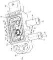
- the pressure sensor of the present embodiment includes a case 10 configured by molding polyphenylene sulfide (that is, PPS), polybutylene terephthalate (that is, PBT), epoxy resin, or the like. Yes.
- a lid 80 described later is omitted.
- the case 10 of the present embodiment includes a main body part 11, a port part 12, an assembly part 13, a connector part 14 and the like provided in the main body part 11.
- the main body 11 has a substantially rectangular parallelepiped shape having one surface 11a and the other surface 11b and first to fourth side surfaces 11c to 11f connecting the one surface 11a and the other surface 11b.
- Two port portions 12 are provided on the first side surface 11c of the main body portion 11 so as to extend along the normal direction of the first side surface 11c.
- the assembly part 13 is provided on the second side surface 11 d of the main body part 11.
- the connector part 14 is provided on the fourth side surface 11f of the main body part 11, and has a cylindrical shape having a cavity inside.
- the case 10 is formed with a pressure introduction hole 15 into which the measurement medium is introduced.
- the pressure introducing hole 15 is configured by connecting a first introducing hole 15 a formed in the main body portion 11 and a second introducing hole 15 b formed in the main body portion 11 and the port portion 12.
- the case 10 has a recess 16 formed on one surface 11a of the main body 11, and the first introduction hole 15a is formed from the bottom surface of the recess 16 toward the other surface 11b.
- the second introduction hole 15b penetrates the port portion 12 and is also formed in the main body portion 11 along the extending direction of the port portion 12, and communicates with the first introduction hole 15a.
- the pressure introducing hole 15 penetrating the case 10 is formed in this way.
- a wiring board 20 composed of a printed board or the like is mounted via an adhesive (not shown).
- a plurality of electronic components 50 such as two sensor chips 30, a circuit chip 40, and a capacitor are mounted on one surface 20 a opposite to the case 10 side.
- the wiring board 20 has a plurality of pad portions 21 formed on one surface 20 a and two through holes 22 communicating with each pressure introducing hole 15.
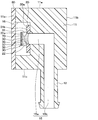
- Each sensor chip 30 has a rectangular silicon substrate 31, and a recess 33 is formed on the other surface 31b side of the silicon substrate 31, so that a diaphragm 33 is formed on the one surface 31a side.
- a gauge resistor (not shown) is formed on the silicon substrate 31 so as to form a bridge circuit on the diaphragm 33. That is, in the sensor chip 30 of the present embodiment, when pressure is applied to the diaphragm 33, the resistance value of the gauge resistance changes, the voltage of the bridge circuit changes, and a semiconductor signal that outputs a sensor signal corresponding to the change in voltage It is a diaphragm type.
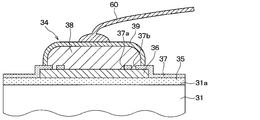
- the sensor chip 30 is formed with a pad portion 34 that is electrically connected to the circuit chip 40.
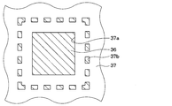
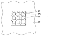
- FIG. 4 is a plan view showing the positional relationship between the first metal film 36 and the insulating film 37 in the vicinity of the contact hole 37a, but the first metal film 36 is hatched for easy understanding. .
- the silicon substrate 31 has a protective film 35 formed of a nitride film or the like on one surface 31a.
- a first metal film 36 is formed on the surface of the protective film 35. Note that a contact hole is formed in the protective film 35 in a cross section different from that in FIG. 3, and the first metal film 36 is electrically connected to the gauge resistance through the contact hole formed in the protective film 35. . That is, the first metal film 36 is a metal film that functions as a wiring portion, and is appropriately routed over the protective film 35. In the present embodiment, the first metal film 36 is made of, for example, aluminum or an alloy containing aluminum as a main component.
- an insulating film 37 made of an oxide film or the like is formed on the surface of the protective film 35 so as to cover the first metal film 36.
- a contact hole 37 a is formed in the insulating film 37 to expose a predetermined region of the first metal film 36.
- the contact hole 37a has a planar rectangular opening end.
- a second metal film 38 is formed on the first metal film 36. Specifically, the second metal film 38 is formed from the first metal film 36 exposed from the contact hole 37 a to a portion around the contact hole 37 a in the insulating film 37. That is, a portion of the insulating film 37 around the contact hole 37a is sandwiched between the first metal film 36 and the second metal film 38.
- the second metal film 38 is made of, for example, nickel or an alloy containing nickel as a main component.
- the insulating film 37 is formed with a slit 37b in a portion located between the first metal film 36 and the second metal film 38.
- the slit 37b has a frame shape surrounding the contact hole 37a, and is formed so as to expose the first metal film 36. That is, the first metal film 36 of the present embodiment is exposed from the contact hole 37a and the slit 37b.
- the slit 37b corresponds to a stress reducing structure.
- the 2nd metal film 38 is also arrange
- FIG. A third metal film 39 is formed on the second metal film 38 so as to cover the surface of the second metal film 38.
- the third metal film 39 is made of a material having corrosion resistance, for example, gold or an alloy containing gold as a main component.
- the first metal film 36, the second metal film 38, and the third metal film 39 are laminated in this manner to form the pad portion 34.
- the above is the configuration of the sensor chip 30 in the present embodiment.
- the pad portion 34 is connected to the third metal film 39 with a bonding wire 60 and is electrically connected to the circuit chip 40 via the bonding wire 60.
- the bonding wire 60 is made of gold, aluminum, or the like.
- each sensor chip 30 is in a state where the other surface 31 b side of the silicon substrate 31 is directed to the wiring substrate 20 so as to close each through hole 22 formed in the wiring substrate 20. It is mounted on the wiring board 20 via an adhesive (not shown). Thereby, the measurement medium introduced into the pressure introducing hole 15 is applied to the sensor chip 30.
- the circuit chip 40 outputs a drive signal to each sensor chip 30 and outputs a detection signal to the outside, and also receives a sensor signal from the sensor chip 30 and amplifies and performs arithmetic processing on the sensor signal. And a control circuit for outputting to.
- the circuit chip 40 has a plurality of pad portions 41, and some of the plurality of pad portions 41 are electrically connected to the pad portions 34 of the sensor chip 30 via bonding wires 60. Further, the remainder of the plurality of pad portions 41 is electrically connected to the pad portions 21 formed on the wiring substrate 20 via bonding wires 61.
- the circuit chip 40 is mounted between the two sensor chips 30.
- a gel-like protective member 70 is disposed in each through hole 22 of the wiring board 20 and the recess 32 of the sensor chip 30.
- the protection member 70 is for protecting the wiring board 20 and the sensor chip 30 from corrosive gas and humidity contained in the measurement medium. That is, in the present embodiment, the pressure of the measurement medium is applied to the diaphragm 33 via the protective member 70.
- the protective member 70 for example, fluorine gel, silicon gel, fluorosilicon gel, or the like is used.
- fluorine gel for example, fluorine gel, silicon gel, fluorosilicon gel, or the like is used.
- the condensed water due to the exhaust gas has strong acidity because the nitrogen oxides and sulfur oxides contained in the exhaust gas are dissolved therein, so that the protective member 70 has high acid resistance. It is preferable to use a fluorine gel.
- the case 10 includes a plurality of metal terminals 17, and each terminal 17 is held in the case 10 by being integrally formed with the case 10 by insert molding. ing.
- each terminal 17 is held so as to penetrate the case 10, and one end portion projects into the recess 16 and the other end portion projects into the connector portion 14.
- Each terminal 17 is electrically connected to a pad portion 21 formed on the wiring board 20 through a bonding wire 62 at one end protruding into the recess 16. The other end of the terminal 17 protruding into the connector 14 is exposed in the connector 14 and is electrically connected to an external wiring member or the like.
- the case 10 is provided with a lid 80 so as to close the recess 16.
- the lid 80 is made of polyphenylene sulfide, polybutylene terephthalate, epoxy resin, or the like, and is provided in the case 10 via an adhesive or the like. As a result, the space surrounded by the recess 16 and the lid 80 is sealed to form a reference pressure chamber.
- the fixing hole 13a is configured by fitting a metal ring into the wall surface of the through hole formed in the resin constituting the assembly portion 13.
- the pressure sensor is installed, for example, such that the upstream exhaust of the DPF is introduced into one of the pressure introduction holes 15 and the downstream exhaust of the DPF is introduced into the other of the pressure introduction holes 15. Thereby, the upstream pressure is detected by one sensor chip 30, and the downstream pressure is detected by the other sensor chip 30.
- the circuit chip 40 the difference between the upstream pressure and the downstream pressure is calculated, and the calculation result is output to the external circuit via the terminal 17. Therefore, the differential pressure in the exhaust pipe before and after the DPF is detected from the calculation result.
- the slit 37b that exposes the first metal film 36 is formed in a portion of the insulating film 37 located between the first metal film 36 and the second metal film 38. Yes.
- a second metal film 38 is also disposed in the slit 37b. For this reason, compared with the case where the slit 37b is not formed in the insulating film 37, it is possible to suppress the cracks from being introduced into the first metal film 36 and the pad portion 34 from being destroyed. That is, the reliability of the pad portion 34 can be improved.
- the first metal film 36 has a portion that contacts the insulating film 37 and the second metal film 38 (hereinafter referred to as a triple point portion).
- the end of the portion exposed from the contact hole 37a in the first metal film 36 is a triple point portion.
- a big stress is applied by the thermal contraction and thermal expansion of the insulating film 37 and the 2nd metal film 38, and it is easy to introduce a crack.
- the slit 37b is formed in the insulating film 37, and the second metal film 38 is also disposed in the slit 37b.
- the end portion of the first metal film 36 exposed from the contact hole 37a and the end portion of the portion exposed from the slit 37b are triple point portions. Therefore, in the present embodiment, the triple point portion in the first metal film 36 can be increased, and the stress generated per unit portion of the triple point portion can be reduced. Thereby, it can suppress that a crack is introduced into the 1st metal film 36, and the reliability of the pad part 34 can be improved.
- the slit 37b may not have a frame shape.
- the slit 37b may be divided into a plurality of pieces. That is, the slit 37b may be formed in a dotted line shape.
- FIG. 5 is a plan view showing the positional relationship between the first metal film 36 and the insulating film 37 in the vicinity of the contact hole 37a, but the first metal film 36 is hatched for easy understanding. .
- the contact holes 37a are formed in a lattice shape. That is, the contact hole 37a is formed so that the insulating film 37 remains in the contact hole 37a. In the present embodiment, the contact hole 37a is formed so that the insulating film 37 remains in a dot shape in the contact hole 37a.
- FIG. 6 is a plan view showing the positional relationship between the first metal film 36 and the insulating film 37 in the vicinity of the contact hole 37a, but the first metal film 36 is hatched for easy understanding.
- the insulating film 37 existing in the contact hole 37a corresponds to a stress reducing structure.
- the lattice-shaped contact holes 37a correspond to a stress reduction structure.
- the contact hole 37a of the present embodiment has a cylindrical shape with a circular opening end. That is, the contact hole 37a does not have a corner.
- the shape of the contact hole 37a corresponds to a stress reducing structure.
- Such a contact hole 37a does not have corners as compared with a conventional contact hole having a rectangular opening end, so that it is possible to prevent stress from being concentrated on a specific portion of the contact hole 37a. For this reason, it can suppress that a crack is introduce
- the contact hole 37 a may have a plurality of side surfaces with different surface directions, and a portion connecting adjacent side surfaces may be a curved surface. In other words, the contact hole 37a may have a shape with a chamfered corner. Such a contact hole 37a can also suppress the concentration of stress at a specific location of the contact hole 37a, so that the same effect as that of the third embodiment can be obtained.
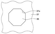
- the contact hole 37a of the present embodiment has an octagonal cylindrical shape with an open end having an octagonal shape.
- the shape of the contact hole 37a corresponds to a stress reducing structure.
- Such a contact hole 37a has a shape having corners, but the number of corners is larger than that of a conventional contact hole having a rectangular shape, and the stress generated in one corner can be reduced. For this reason, it can suppress that a crack is introduce
- the case where the opening end of the contact hole 37a has an octagonal shape has been described as an example.
- the contact hole 37a has a larger number of corners than when the open end is rectangular, the contact hole 37a has a pentagonal or more open end. It suffices if the polygonal shape is used.
- the thickness of the third metal film 39 is defined with respect to the first embodiment. Since other aspects are the same as those in the first embodiment, description thereof is omitted here.
- the configuration of the pressure sensor of the present embodiment is basically the same as that of the first embodiment, but the slit 34b is not formed.
- the third metal film 39 is composed of a gold film, and the film thickness is defined.
- the inventors first focused on the relationship between the thickness of the third metal film 39 and the number of pinholes formed in the third metal film 39, and conducted a nitric acid explosion test to perform FIG. The result shown in was obtained.
- the pinhole constitutes a passage through which a corrosive medium containing chlorine or the like reaches the second metal film 38. For this reason, the second metal film 38 is more easily corroded as the number of pinholes is larger.
- pinholes increase sharply when the thickness of the third metal film 39 is less than 0.4 ⁇ m, and are hardly formed when the thickness is 0.4 ⁇ m or more.
- the inventors focused on the relationship between the film thickness of the third metal film 39 and the shear strength, and conducted a tensile test to obtain the result shown in FIG. As shown in FIG. 11, it is confirmed that the shear strength increases sharply when it becomes 0.4 ⁇ m or more.
- the fact that pinholes are almost absent in the third metal film 39 suppresses the corrosion of the second metal film 38 and the third metal film 39. It is presumed that this is because it becomes difficult for the part that becomes the starting point of destruction to exist.
- the third metal film 39 has a thickness of 0.4 ⁇ m or more.
- the third metal film 39 is made of a gold film and has a thickness of 0.4 ⁇ m or more. For this reason, the number of pinholes in the third metal film 39 can be almost eliminated, and the shear strength can be increased. Therefore, the pad portion 34 can be prevented from being broken, and the reliability of the pad portion 34 can be improved.
- each of the above embodiments has been described as an example.
- each of the above embodiments may be applied to an acceleration sensor or an angular velocity sensor.
- the pad portion 34 formed on the sensor chip 30 has been described. However, each of the above embodiments may be applied to the pad portion 21 of the wiring board 20, the pad portion 41 of the circuit chip 40, and the like.
- the third metal film 39 may not be provided.
- the insulating film 37 remaining in the contact hole 37a may not be arranged in a dot shape, and the shape of the insulating film 37 remaining in the contact hole 37a can be appropriately changed.
- the 3rd metal film 39 may be comprised with the alloy which has gold as a main component.
- the third metal film 39 is made of an alloy containing gold as a main component, the same effect as that of the fifth embodiment can be obtained by setting the thickness of the third metal film 39 to 0.4 ⁇ m or more. Can be obtained.
- the above embodiments can be combined as appropriate.
- the first embodiment may be combined with the fifth embodiment, and the slit 37 b may be formed in the insulating film 37.
- the second embodiment may be combined with the third to fifth embodiments, and the contact holes 37a may be formed in a lattice shape.
- the insulating film 37 remains in the contact hole 37a, and the outermost portion of the contact hole 37a is the third and fourth. What is necessary is just to make it become the structure of embodiment.
- the third and fourth embodiments may be combined with the fifth embodiment, and the contact hole 37a may have a circular opening at the opening end or a polygonal shape having a pentagon or more opening opening. Good.
Landscapes
- Engineering & Computer Science (AREA)
- Microelectronics & Electronic Packaging (AREA)
- Physics & Mathematics (AREA)
- General Physics & Mathematics (AREA)
- Computer Hardware Design (AREA)
- Chemical & Material Sciences (AREA)
- Analytical Chemistry (AREA)
- Manufacturing & Machinery (AREA)
- Pressure Sensors (AREA)
- Measuring Fluid Pressure (AREA)
- Wire Bonding (AREA)
Priority Applications (3)
| Application Number | Priority Date | Filing Date | Title |
|---|---|---|---|
| CN201980017122.2A CN111819428A (zh) | 2018-03-06 | 2019-03-05 | 电子装置 |
| DE112019001185.5T DE112019001185T5 (de) | 2018-03-06 | 2019-03-05 | Elektronische vorrichtung |
| US17/011,062 US20200399118A1 (en) | 2018-03-06 | 2020-09-03 | Electronic device |
Applications Claiming Priority (2)
| Application Number | Priority Date | Filing Date | Title |
|---|---|---|---|
| JP2018039959A JP2019152625A (ja) | 2018-03-06 | 2018-03-06 | 電子装置 |
| JP2018-039959 | 2018-03-06 |
Related Child Applications (1)
| Application Number | Title | Priority Date | Filing Date |
|---|---|---|---|
| US17/011,062 Continuation US20200399118A1 (en) | 2018-03-06 | 2020-09-03 | Electronic device |
Publications (1)
| Publication Number | Publication Date |
|---|---|
| WO2019172263A1 true WO2019172263A1 (ja) | 2019-09-12 |
Family
ID=67846676
Family Applications (1)
| Application Number | Title | Priority Date | Filing Date |
|---|---|---|---|
| PCT/JP2019/008659 Ceased WO2019172263A1 (ja) | 2018-03-06 | 2019-03-05 | 電子装置 |
Country Status (5)
| Country | Link |
|---|---|
| US (1) | US20200399118A1 (https=) |
| JP (1) | JP2019152625A (https=) |
| CN (1) | CN111819428A (https=) |
| DE (1) | DE112019001185T5 (https=) |
| WO (1) | WO2019172263A1 (https=) |
Families Citing this family (1)
| Publication number | Priority date | Publication date | Assignee | Title |
|---|---|---|---|---|
| JP7127471B2 (ja) * | 2018-10-12 | 2022-08-30 | 株式会社デンソー | 半導体モジュール |
Citations (3)
| Publication number | Priority date | Publication date | Assignee | Title |
|---|---|---|---|---|
| JP2001351920A (ja) * | 2000-06-07 | 2001-12-21 | Mitsubishi Electric Corp | 半導体装置およびその製造方法 |
| KR20080105836A (ko) * | 2007-06-01 | 2008-12-04 | 주식회사 동부하이텍 | 반도체 장치 형성 방법 |
| JP2015210082A (ja) * | 2014-04-23 | 2015-11-24 | 株式会社デンソー | 半導体装置 |
Family Cites Families (10)
| Publication number | Priority date | Publication date | Assignee | Title |
|---|---|---|---|---|
| JP2000195896A (ja) * | 1998-12-25 | 2000-07-14 | Nec Corp | 半導体装置 |
| JP2003243443A (ja) * | 2002-02-13 | 2003-08-29 | Mitsubishi Electric Corp | 半導体装置 |
| JP4049102B2 (ja) * | 2004-01-21 | 2008-02-20 | 株式会社デンソー | 圧力センサ |
| JP2006200925A (ja) * | 2005-01-18 | 2006-08-03 | Denso Corp | 圧力センサ |
| JP4506478B2 (ja) * | 2005-01-18 | 2010-07-21 | 株式会社デンソー | 圧力センサ |
| WO2007052335A1 (ja) * | 2005-11-01 | 2007-05-10 | Hitachi, Ltd. | 半導体圧力センサ |
| JP2011040669A (ja) * | 2009-08-18 | 2011-02-24 | Elpida Memory Inc | 半導体装置 |
| JP6301763B2 (ja) * | 2014-07-16 | 2018-03-28 | ルネサスエレクトロニクス株式会社 | 半導体装置、および半導体装置の製造方法 |
| JP6571414B2 (ja) * | 2015-06-30 | 2019-09-04 | エイブリック株式会社 | 半導体装置 |
| WO2018037736A1 (ja) * | 2016-08-22 | 2018-03-01 | 三菱電機株式会社 | 半導体装置 |
-
2018
- 2018-03-06 JP JP2018039959A patent/JP2019152625A/ja active Pending
-
2019
- 2019-03-05 CN CN201980017122.2A patent/CN111819428A/zh active Pending
- 2019-03-05 WO PCT/JP2019/008659 patent/WO2019172263A1/ja not_active Ceased
- 2019-03-05 DE DE112019001185.5T patent/DE112019001185T5/de not_active Withdrawn
-
2020
- 2020-09-03 US US17/011,062 patent/US20200399118A1/en not_active Abandoned
Patent Citations (3)
| Publication number | Priority date | Publication date | Assignee | Title |
|---|---|---|---|---|
| JP2001351920A (ja) * | 2000-06-07 | 2001-12-21 | Mitsubishi Electric Corp | 半導体装置およびその製造方法 |
| KR20080105836A (ko) * | 2007-06-01 | 2008-12-04 | 주식회사 동부하이텍 | 반도체 장치 형성 방법 |
| JP2015210082A (ja) * | 2014-04-23 | 2015-11-24 | 株式会社デンソー | 半導体装置 |
Also Published As
| Publication number | Publication date |
|---|---|
| DE112019001185T5 (de) | 2020-12-10 |
| US20200399118A1 (en) | 2020-12-24 |
| JP2019152625A (ja) | 2019-09-12 |
| CN111819428A (zh) | 2020-10-23 |
Similar Documents
| Publication | Publication Date | Title |
|---|---|---|
| EP1980830B1 (en) | Pressure sensor device including temperature sensor contained in common housing | |
| CN104681500B (zh) | 物理量测定传感器 | |
| JP4940786B2 (ja) | 圧力センサ | |
| JPWO2007052335A1 (ja) | 半導体圧力センサ | |
| US20140216146A1 (en) | Air physical quantity sensing device | |
| US7284435B2 (en) | Pressure sensor | |
| JP3915605B2 (ja) | 圧力センサ装置 | |
| WO2019172263A1 (ja) | 電子装置 | |
| JP2004279091A (ja) | 圧力センサ | |
| JP6387912B2 (ja) | 圧力センサ | |
| US7036384B2 (en) | Pressure sensor | |
| JP2009047670A (ja) | 圧力センサ | |
| US20050250371A1 (en) | Sealing structure for connector | |
| JP4497219B2 (ja) | 圧力センサおよびその製造方法 | |
| JP4506478B2 (ja) | 圧力センサ | |
| JP3556166B2 (ja) | 圧力センサ | |
| JP4207847B2 (ja) | 圧力センサ | |
| JP5494741B2 (ja) | 圧力センサ | |
| JP4168813B2 (ja) | 圧力センサ装置 | |
| JP2018105748A (ja) | 圧力センサ | |
| US6008639A (en) | Magnetic sensor having a main electrical circuit base with a crack forming area | |
| JP5251498B2 (ja) | 圧力センサ | |
| CN121475512A (zh) | 用于测量介质中压力的装置 | |
| JP4882682B2 (ja) | 圧力センサ装置 | |
| JP5067360B2 (ja) | 圧力センサ |
Legal Events
| Date | Code | Title | Description |
|---|---|---|---|
| 121 | Ep: the epo has been informed by wipo that ep was designated in this application |
Ref document number: 19765063 Country of ref document: EP Kind code of ref document: A1 |
|
| 122 | Ep: pct application non-entry in european phase |
Ref document number: 19765063 Country of ref document: EP Kind code of ref document: A1 |