WO2019163340A1 - 放射冷却装置 - Google Patents
放射冷却装置 Download PDFInfo
- Publication number
- WO2019163340A1 WO2019163340A1 PCT/JP2019/001338 JP2019001338W WO2019163340A1 WO 2019163340 A1 WO2019163340 A1 WO 2019163340A1 JP 2019001338 W JP2019001338 W JP 2019001338W WO 2019163340 A1 WO2019163340 A1 WO 2019163340A1
- Authority
- WO
- WIPO (PCT)
- Prior art keywords
- layer
- silver
- light
- cooling device
- thickness
- Prior art date
Links
- 238000001816 cooling Methods 0.000 title claims abstract description 159
- 230000005855 radiation Effects 0.000 claims abstract description 158
- 229910052709 silver Inorganic materials 0.000 claims abstract description 123
- BQCADISMDOOEFD-UHFFFAOYSA-N Silver Chemical compound [Ag] BQCADISMDOOEFD-UHFFFAOYSA-N 0.000 claims abstract description 120
- 239000004332 silver Substances 0.000 claims abstract description 120
- 229910052782 aluminium Inorganic materials 0.000 claims abstract description 84
- XAGFODPZIPBFFR-UHFFFAOYSA-N aluminium Chemical compound [Al] XAGFODPZIPBFFR-UHFFFAOYSA-N 0.000 claims abstract description 82
- 238000005275 alloying Methods 0.000 claims abstract description 48
- 229910001316 Ag alloy Inorganic materials 0.000 claims abstract description 22
- 229910000838 Al alloy Inorganic materials 0.000 claims abstract description 19
- 150000004767 nitrides Chemical class 0.000 claims description 34
- 239000000758 substrate Substances 0.000 claims description 13
- 230000002265 prevention Effects 0.000 claims description 11
- 239000003963 antioxidant agent Substances 0.000 claims description 9
- 230000003078 antioxidant effect Effects 0.000 claims description 9
- 239000011521 glass Substances 0.000 claims description 9
- 239000005388 borosilicate glass Substances 0.000 claims description 6
- 239000005331 crown glasses (windows) Substances 0.000 claims description 6
- 229910045601 alloy Inorganic materials 0.000 abstract description 4
- 239000000956 alloy Substances 0.000 abstract description 4
- 230000000694 effects Effects 0.000 abstract description 4
- 238000010030 laminating Methods 0.000 abstract description 3
- 230000003287 optical effect Effects 0.000 abstract description 2
- 230000002035 prolonged effect Effects 0.000 abstract 1
- 239000010408 film Substances 0.000 description 145
- 239000013256 coordination polymer Substances 0.000 description 30
- 229910018072 Al 2 O 3 Inorganic materials 0.000 description 26
- 229910052760 oxygen Inorganic materials 0.000 description 23
- NDVLTYZPCACLMA-UHFFFAOYSA-N silver oxide Chemical class [O-2].[Ag+].[Ag+] NDVLTYZPCACLMA-UHFFFAOYSA-N 0.000 description 23
- 239000000463 material Substances 0.000 description 22
- 239000001301 oxygen Substances 0.000 description 22
- QVGXLLKOCUKJST-UHFFFAOYSA-N atomic oxygen Chemical compound [O] QVGXLLKOCUKJST-UHFFFAOYSA-N 0.000 description 20
- 229910052751 metal Inorganic materials 0.000 description 19
- 239000002184 metal Substances 0.000 description 19
- 238000010521 absorption reaction Methods 0.000 description 14
- 238000004544 sputter deposition Methods 0.000 description 14
- 238000004519 manufacturing process Methods 0.000 description 13
- 229910001923 silver oxide Inorganic materials 0.000 description 11
- 238000002834 transmittance Methods 0.000 description 11
- 230000031700 light absorption Effects 0.000 description 10
- 229910004298 SiO 2 Inorganic materials 0.000 description 9
- 230000008859 change Effects 0.000 description 9
- VYPSYNLAJGMNEJ-UHFFFAOYSA-N Silicium dioxide Chemical compound O=[Si]=O VYPSYNLAJGMNEJ-UHFFFAOYSA-N 0.000 description 8
- 238000006243 chemical reaction Methods 0.000 description 7
- TWNQGVIAIRXVLR-UHFFFAOYSA-N oxo(oxoalumanyloxy)alumane Chemical compound O=[Al]O[Al]=O TWNQGVIAIRXVLR-UHFFFAOYSA-N 0.000 description 7
- 238000007740 vapor deposition Methods 0.000 description 7
- 229910052581 Si3N4 Inorganic materials 0.000 description 6
- 238000000034 method Methods 0.000 description 6
- 230000035699 permeability Effects 0.000 description 6
- HQVNEWCFYHHQES-UHFFFAOYSA-N silicon nitride Chemical group N12[Si]34N5[Si]62N3[Si]51N64 HQVNEWCFYHHQES-UHFFFAOYSA-N 0.000 description 6
- 230000009471 action Effects 0.000 description 5
- 230000015572 biosynthetic process Effects 0.000 description 5
- KDLHZDBZIXYQEI-UHFFFAOYSA-N Palladium Chemical compound [Pd] KDLHZDBZIXYQEI-UHFFFAOYSA-N 0.000 description 4
- 229910010413 TiO 2 Inorganic materials 0.000 description 4
- 230000007423 decrease Effects 0.000 description 4
- 239000000203 mixture Substances 0.000 description 4
- 235000012239 silicon dioxide Nutrition 0.000 description 4
- 239000000377 silicon dioxide Substances 0.000 description 4
- DTPQZKZONQKKSU-UHFFFAOYSA-N silver azanide silver Chemical compound [NH2-].[Ag].[Ag].[Ag+] DTPQZKZONQKKSU-UHFFFAOYSA-N 0.000 description 4
- 238000001228 spectrum Methods 0.000 description 4
- RYGMFSIKBFXOCR-UHFFFAOYSA-N Copper Chemical compound [Cu] RYGMFSIKBFXOCR-UHFFFAOYSA-N 0.000 description 3
- 230000005540 biological transmission Effects 0.000 description 3
- 229910052802 copper Inorganic materials 0.000 description 3
- 239000010949 copper Substances 0.000 description 3
- 238000010438 heat treatment Methods 0.000 description 3
- 239000012466 permeate Substances 0.000 description 3
- FYYHWMGAXLPEAU-UHFFFAOYSA-N Magnesium Chemical compound [Mg] FYYHWMGAXLPEAU-UHFFFAOYSA-N 0.000 description 2
- PXHVJJICTQNCMI-UHFFFAOYSA-N Nickel Chemical compound [Ni] PXHVJJICTQNCMI-UHFFFAOYSA-N 0.000 description 2
- HCHKCACWOHOZIP-UHFFFAOYSA-N Zinc Chemical compound [Zn] HCHKCACWOHOZIP-UHFFFAOYSA-N 0.000 description 2
- GEIAQOFPUVMAGM-UHFFFAOYSA-N ZrO Inorganic materials [Zr]=O GEIAQOFPUVMAGM-UHFFFAOYSA-N 0.000 description 2
- 230000003064 anti-oxidating effect Effects 0.000 description 2
- 230000001747 exhibiting effect Effects 0.000 description 2
- 239000005357 flat glass Substances 0.000 description 2
- 239000007789 gas Substances 0.000 description 2
- 238000003475 lamination Methods 0.000 description 2
- 230000007774 longterm Effects 0.000 description 2
- 229910052749 magnesium Inorganic materials 0.000 description 2
- 239000011777 magnesium Substances 0.000 description 2
- 230000003647 oxidation Effects 0.000 description 2
- 238000007254 oxidation reaction Methods 0.000 description 2
- 229910052763 palladium Inorganic materials 0.000 description 2
- 230000009257 reactivity Effects 0.000 description 2
- 229910052710 silicon Inorganic materials 0.000 description 2
- 239000000126 substance Substances 0.000 description 2
- 239000013077 target material Substances 0.000 description 2
- 229910052725 zinc Inorganic materials 0.000 description 2
- 239000011701 zinc Substances 0.000 description 2
- 229910000975 Carbon steel Inorganic materials 0.000 description 1
- 229910005191 Ga 2 O 3 Inorganic materials 0.000 description 1
- 229910052688 Gadolinium Inorganic materials 0.000 description 1
- 229910005793 GeO 2 Inorganic materials 0.000 description 1
- 229910018068 Li 2 O Inorganic materials 0.000 description 1
- XUIMIQQOPSSXEZ-UHFFFAOYSA-N Silicon Chemical compound [Si] XUIMIQQOPSSXEZ-UHFFFAOYSA-N 0.000 description 1
- 229910006404 SnO 2 Inorganic materials 0.000 description 1
- 229910052771 Terbium Inorganic materials 0.000 description 1
- ATJFFYVFTNAWJD-UHFFFAOYSA-N Tin Chemical compound [Sn] ATJFFYVFTNAWJD-UHFFFAOYSA-N 0.000 description 1
- GWEVSGVZZGPLCZ-UHFFFAOYSA-N Titan oxide Chemical compound O=[Ti]=O GWEVSGVZZGPLCZ-UHFFFAOYSA-N 0.000 description 1
- RTAQQCXQSZGOHL-UHFFFAOYSA-N Titanium Chemical compound [Ti] RTAQQCXQSZGOHL-UHFFFAOYSA-N 0.000 description 1
- 230000032900 absorption of visible light Effects 0.000 description 1
- 230000008901 benefit Effects 0.000 description 1
- 229910052795 boron group element Inorganic materials 0.000 description 1
- 229910052800 carbon group element Inorganic materials 0.000 description 1
- 239000010962 carbon steel Substances 0.000 description 1
- 230000007797 corrosion Effects 0.000 description 1
- 238000005260 corrosion Methods 0.000 description 1
- 230000007547 defect Effects 0.000 description 1
- 230000006866 deterioration Effects 0.000 description 1
- 238000010586 diagram Methods 0.000 description 1
- 238000002845 discoloration Methods 0.000 description 1
- 238000009826 distribution Methods 0.000 description 1
- UIWYJDYFSGRHKR-UHFFFAOYSA-N gadolinium atom Chemical compound [Gd] UIWYJDYFSGRHKR-UHFFFAOYSA-N 0.000 description 1
- PCHJSUWPFVWCPO-UHFFFAOYSA-N gold Chemical compound [Au] PCHJSUWPFVWCPO-UHFFFAOYSA-N 0.000 description 1
- 229910052737 gold Inorganic materials 0.000 description 1
- 239000010931 gold Substances 0.000 description 1
- 229910021480 group 4 element Inorganic materials 0.000 description 1
- 229910021478 group 5 element Inorganic materials 0.000 description 1
- 230000006872 improvement Effects 0.000 description 1
- 229910052746 lanthanum Inorganic materials 0.000 description 1
- FZLIPJUXYLNCLC-UHFFFAOYSA-N lanthanum atom Chemical compound [La] FZLIPJUXYLNCLC-UHFFFAOYSA-N 0.000 description 1
- ORUIBWPALBXDOA-UHFFFAOYSA-L magnesium fluoride Chemical compound [F-].[F-].[Mg+2] ORUIBWPALBXDOA-UHFFFAOYSA-L 0.000 description 1
- WPBNNNQJVZRUHP-UHFFFAOYSA-L manganese(2+);methyl n-[[2-(methoxycarbonylcarbamothioylamino)phenyl]carbamothioyl]carbamate;n-[2-(sulfidocarbothioylamino)ethyl]carbamodithioate Chemical compound [Mn+2].[S-]C(=S)NCCNC([S-])=S.COC(=O)NC(=S)NC1=CC=CC=C1NC(=S)NC(=O)OC WPBNNNQJVZRUHP-UHFFFAOYSA-L 0.000 description 1
- 150000002739 metals Chemical class 0.000 description 1
- 229910052759 nickel Inorganic materials 0.000 description 1
- 229910000510 noble metal Inorganic materials 0.000 description 1
- 238000005546 reactive sputtering Methods 0.000 description 1
- 230000009467 reduction Effects 0.000 description 1
- 238000002310 reflectometry Methods 0.000 description 1
- 239000010703 silicon Substances 0.000 description 1
- VFWRGKJLLYDFBY-UHFFFAOYSA-N silver;hydrate Chemical compound O.[Ag].[Ag] VFWRGKJLLYDFBY-UHFFFAOYSA-N 0.000 description 1
- GZCRRIHWUXGPOV-UHFFFAOYSA-N terbium atom Chemical compound [Tb] GZCRRIHWUXGPOV-UHFFFAOYSA-N 0.000 description 1
- 239000010409 thin film Substances 0.000 description 1
- 239000011135 tin Substances 0.000 description 1
- 229910052718 tin Inorganic materials 0.000 description 1
- 229910052719 titanium Inorganic materials 0.000 description 1
- 239000010936 titanium Substances 0.000 description 1
- 229910052727 yttrium Inorganic materials 0.000 description 1
- VWQVUPCCIRVNHF-UHFFFAOYSA-N yttrium atom Chemical compound [Y] VWQVUPCCIRVNHF-UHFFFAOYSA-N 0.000 description 1
Images


Classifications
-
- F—MECHANICAL ENGINEERING; LIGHTING; HEATING; WEAPONS; BLASTING
- F28—HEAT EXCHANGE IN GENERAL
- F28F—DETAILS OF HEAT-EXCHANGE AND HEAT-TRANSFER APPARATUS, OF GENERAL APPLICATION
- F28F21/00—Constructions of heat-exchange apparatus characterised by the selection of particular materials
- F28F21/08—Constructions of heat-exchange apparatus characterised by the selection of particular materials of metal
- F28F21/081—Heat exchange elements made from metals or metal alloys
-
- F—MECHANICAL ENGINEERING; LIGHTING; HEATING; WEAPONS; BLASTING
- F28—HEAT EXCHANGE IN GENERAL
- F28F—DETAILS OF HEAT-EXCHANGE AND HEAT-TRANSFER APPARATUS, OF GENERAL APPLICATION
- F28F13/00—Arrangements for modifying heat-transfer, e.g. increasing, decreasing
- F28F13/18—Arrangements for modifying heat-transfer, e.g. increasing, decreasing by applying coatings, e.g. radiation-absorbing, radiation-reflecting; by surface treatment, e.g. polishing
-
- B—PERFORMING OPERATIONS; TRANSPORTING
- B32—LAYERED PRODUCTS
- B32B—LAYERED PRODUCTS, i.e. PRODUCTS BUILT-UP OF STRATA OF FLAT OR NON-FLAT, e.g. CELLULAR OR HONEYCOMB, FORM
- B32B15/00—Layered products comprising a layer of metal
- B32B15/04—Layered products comprising a layer of metal comprising metal as the main or only constituent of a layer, which is next to another layer of the same or of a different material
- B32B15/043—Layered products comprising a layer of metal comprising metal as the main or only constituent of a layer, which is next to another layer of the same or of a different material of metal
-
- B—PERFORMING OPERATIONS; TRANSPORTING
- B32—LAYERED PRODUCTS
- B32B—LAYERED PRODUCTS, i.e. PRODUCTS BUILT-UP OF STRATA OF FLAT OR NON-FLAT, e.g. CELLULAR OR HONEYCOMB, FORM
- B32B17/00—Layered products essentially comprising sheet glass, or glass, slag, or like fibres
- B32B17/06—Layered products essentially comprising sheet glass, or glass, slag, or like fibres comprising glass as the main or only constituent of a layer, next to another layer of a specific material
- B32B17/061—Layered products essentially comprising sheet glass, or glass, slag, or like fibres comprising glass as the main or only constituent of a layer, next to another layer of a specific material of metal
-
- G—PHYSICS
- G02—OPTICS
- G02B—OPTICAL ELEMENTS, SYSTEMS OR APPARATUS
- G02B5/00—Optical elements other than lenses
- G02B5/20—Filters
- G02B5/208—Filters for use with infrared or ultraviolet radiation, e.g. for separating visible light from infrared and/or ultraviolet radiation
-
- G—PHYSICS
- G02—OPTICS
- G02B—OPTICAL ELEMENTS, SYSTEMS OR APPARATUS
- G02B5/00—Optical elements other than lenses
- G02B5/20—Filters
- G02B5/26—Reflecting filters
Definitions
- the present invention provides a radiation in which an infrared radiation layer that radiates infrared light from a radiation surface and a light reflection layer that is positioned on the opposite side of the radiation surface on the side where the radiation surface is present are stacked.
- the present invention relates to a cooling device.
- Such a radiation cooling device transmits infrared light radiated from the radiation surface of the infrared radiation layer through an atmospheric window (for example, a window that transmits infrared light having a wavelength of 8 to 13 ⁇ m, etc.) to form a light reflection layer. It is used for cooling various cooling objects such as cooling the cooling object located on the side opposite to the side where the infrared radiation layer is present.
- an atmospheric window for example, a window that transmits infrared light having a wavelength of 8 to 13 ⁇ m, etc.
- the light reflecting layer reflects light (visible light, ultraviolet light, infrared light) transmitted through the infrared radiation layer and emits it from the radiation surface, thereby transmitting light (visible light, Ultraviolet light and infrared light) are projected onto the object to be cooled and the object to be cooled is prevented from being heated.
- the light reflection layer also has a function of reflecting infrared light radiated from the infrared radiation layer to the existence side of the light reflection layer toward the infrared radiation layer.
- the light reflection layer is provided to reflect light (visible light, ultraviolet light, infrared light) transmitted through the infrared radiation layer.
- the light reflection layer is a state in which a metal layer made of silver, a layer of titanium dioxide (TiO 2 ), and a layer of magnesium fluoride (MgF 2 ) are alternately arranged.
- a photoning band cap layer formed in a multilayer state in a state where the photoning band cap layer is positioned on the side close to the infrared radiation layer for example, Patent Document 1). reference.
- the light reflection layer is configured as a metal layer made of aluminum (for example, see Patent Document 2).
- a metal layer made of aluminum is used as a substrate, and an SiO layer and an MgO layer constituting an infrared radiation layer are laminated.
- the light reflecting layer is provided with the photoning band cap layer laminated in a multilayer state, so that there is a disadvantage that the manufacturing becomes complicated. Even if it is provided, the metal layer made of expensive silver cannot be made sufficiently thin, so there is a disadvantage that it is difficult to reduce the overall configuration.
- the light reflecting layer is configured as a metal layer made of aluminum
- the light reflecting layer is configured with inexpensive aluminum
- the overall configuration can be reduced. is there.
- the metal layer made of aluminum is easier to absorb light than silver
- the light transmitted through the infrared radiation layer is absorbed by the metal layer made of aluminum and the temperature rises due to the absorption of the light. Due to the metal layer heating the object to be cooled, there is a possibility that the object to be cooled cannot be appropriately cooled.
- the light reflecting layer is configured as a metal layer made of silver having a thickness of 100 nm or more
- the infrared radiation layer is transmitted.
- the cooling target can be cooled while suppressing the light from being projected onto the cooling target (see FIGS. 12 and 13), and the light reflecting layer is made of a metal made of silver having a thickness of 300 nm or more.
- the light to be transmitted through the infrared radiation layer can be appropriately suppressed from being projected onto the object to be cooled, and the object to be cooled can be appropriately cooled.
- the light reflection layer is configured as a metal layer made of silver having a thickness of 300 nm or more, the radiation cooling device becomes expensive. While suppressing, it was desired to cool the object to be cooled.
- the present invention has been made in view of the above circumstances, and its purpose is to appropriately cool the object to be cooled while reducing the cost of the light reflecting layer, and to provide a cooling action over a long period of time. It is in the point which provides the radiation cooling device which can demonstrate well.
- the radiant cooling device of the present invention includes an infrared radiation layer that radiates infrared light from a radiation surface, and a light reflection layer that is positioned on the opposite side of the radiation surface on the side where the radiation surface exists. It is provided and its characteristic configuration is
- the light reflecting layer includes a first layer made of silver or a silver alloy, a second layer made of aluminum or an aluminum alloy, and an alloying-preventing transparent layer for preventing alloying of silver and aluminum. In this case, the alloying-preventing transparent layer and the second layer are laminated in the order of being positioned on the side closer to the infrared radiation layer.
- the light reflecting layer is composed of a first layer made of silver or a silver alloy and a second layer made of aluminum or an aluminum alloy, and the first layer is close to an infrared radiation layer. It came to discover that it was possible to cool the object to be cooled while suppressing the amount of expensive silver or silver alloy used by forming a laminated state in a form positioned on the side.
- silver or a silver alloy can reflect visible light and infrared light efficiently, but tends to have a low reflectivity for ultraviolet light.
- aluminum or aluminum alloy cannot reflect visible light or infrared light more efficiently than silver or silver alloy, but tends to reflect ultraviolet light efficiently.
- aluminum or aluminum alloy tends to absorb visible light and infrared light more easily than silver or silver alloy.
- the first layer made of silver or a silver alloy and the second layer made of aluminum or an aluminum alloy in a state in which the first layer is positioned so as to be positioned closer to the infrared radiation layer
- the second layer suppresses absorption of visible light or infrared light, and even if the thickness of the first layer is reduced, the first layer
- light visible light, ultraviolet light, infrared light
- the 1st layer which consists of silver or a silver alloy can be made thin, the cost reduction of a light reflection layer can be aimed at.
- an alloying prevention transparent layer for preventing alloying of silver and aluminum is provided between the first layer and the second layer, it is possible to suppress alloying of silver and aluminum. While avoiding light absorption of the light reflecting layer, the state in which the light reflecting layer appropriately reflects light can be maintained for a long period of time, and the cooling effect can be exhibited well over a long period of time.
- the alloying of silver and aluminum gradually progresses, and the reflectance of sunlight in the light reflecting layer is increased.
- the solar absorption is expected to increase. It suppresses alloying of silver and aluminum.
- the object to be cooled can be appropriately cooled while the cost of the light reflecting layer is reduced, and the cooling effect can be exhibited well over a long period of time.
- a further characteristic configuration of the radiant cooling device of the present invention is that the thickness of the first layer is larger than 3.3 nm and not larger than 100 nm.
- the infrared radiation layer is transmitted due to the presence of the second layer. It was found that the object to be cooled can be cooled by appropriately reflecting light (visible light, ultraviolet light, infrared light).
- the thickness of the first layer made of silver or a silver alloy is set to a thin thickness greater than 3.3 nm and less than or equal to 100 nm, the light reflection layer can be sufficiently inexpensive, The object to be cooled can be cooled.
- the thickness of the first layer made of silver or a silver alloy is preferably larger than 3.3 nm and 100 nm or less, preferably 30 nm or more, so that the cooling target can be appropriately set. It can be cooled.
- the object to be cooled can be cooled while sufficiently reducing the cost of the light reflecting layer.
- a further characteristic configuration of the radiation cooling device of the present invention is that the thickness of the first layer is not less than 50 nm and not more than 100 nm.
- the thickness of the first layer made of silver or a silver alloy is in the range of 50 nm to 100 nm, the light (mainly visible light, infrared light) reflecting action by the first layer is appropriately exhibited.
- the presence of the second layer allows the light (visible light, ultraviolet light, infrared light) transmitted through the infrared radiation layer to be appropriately reflected.
- the light reflective layer is made of silver having a thickness of 300 nm or more. It came to discover that the object to be cooled can be cooled with the same capacity as that of the metal layer.
- a further characteristic configuration of the radiant cooling device of the present invention is that the thickness of the second layer is 10 nm or more.
- the second layer reflects ultraviolet light if the thickness of the second layer made of aluminum or aluminum alloy is 10 nm or more. It came to find that the light (visible light, ultraviolet light, infrared light) which permeate
- the thickness of the second layer made of aluminum or aluminum alloy may be 10 nm or more, but in order to suppress the amount of aluminum or aluminum alloy used, it is necessary to avoid making it thicker than necessary.
- the radiation cooling device of the present invention it is possible to reflect the light transmitted through the infrared radiation layer while appropriately exhibiting the action of reflecting the ultraviolet light.
- a further characteristic configuration of the radiation cooling device of the present invention is that the infrared radiation layer is made of any one of alkali-free glass, crown glass, and borosilicate glass.
- alkali-free glass, crown glass, and borosilicate glass are relatively inexpensive, but have excellent transmittance of sunlight (visible light, ultraviolet light, near infrared light) (for example, about 80%). Because it does not absorb sunlight, it emits infrared light having a wavelength equivalent to an atmospheric window (for example, a window that transmits infrared light having a wavelength of 8 to 13 ⁇ m). It has the property of high radiation intensity.
- the infrared radiation layer with any one of alkali-free glass, crown glass, and borosilicate glass, a radiation cooling device with a high cooling capacity can be achieved while reducing the overall configuration. Can be obtained.
- the cooling capacity can be improved while the overall configuration is reduced.
- a further characteristic configuration of the radiation cooling device of the present invention is that the first layer, the alloying-preventing transparent layer, and the second layer are laminated using the infrared radiation layer as a substrate.
- the overall configuration can be simplified and the overall configuration can be reduced in thickness.
- the first layer, the anti-alloying transparent layer and the second layer are laminated with the infrared radiation layer as the substrate, if the first layer, the anti-alloying transparent layer and the second layer are thin, for example, The first layer, the alloying-preventing transparent layer, and the second layer are sequentially laminated by sputtering or the like.
- the second layer, the alloying-preventing transparent layer, and the first layer are sequentially laminated on the lamination substrate by sputtering or the like, and then the presence of the second layer of the first layer.
- a separately prepared infrared radiation layer is placed on the side opposite to the side and laminated, or the part opposite to the side where the first alloying prevention transparent layer is present is sputtered, etc.
- it is not necessary to provide a substrate for stacking so that the overall configuration can be simplified and the overall configuration can be made thinner.
- the overall configuration can be simplified and the overall configuration can be made thinner.
- a further characteristic configuration of the radiation cooling device of the present invention is that an adhesion layer is laminated between the infrared radiation layer and the first layer.
- the adhesion layer is laminated between the infrared radiation layer and the first layer of the light reflection layer, the first layer of the light reflection layer is in contact with the infrared radiation layer due to a temperature change or the like. Since the occurrence of damage such as peeling can be suppressed, durability can be improved.
- a further characteristic configuration of the radiant cooling device of the present invention is that an antioxidant layer is laminated on the second layer opposite to the side where the alloying-preventing transparent layer is present.
- the antioxidant layer is laminated on the opposite side of the second layer made of aluminum or aluminum alloy from the side where the anti-alloying transparent layer is present, the second layer is oxidized even if the second layer is thinned. Therefore, since it can suppress that it deteriorates, durability can be improved.
- the radiant cooling device of the present invention it is possible to suppress the deterioration of the second layer made of aluminum or aluminum alloy and improve the durability.
- a further characteristic configuration of the radiation cooling device of the present invention is that the alloying-preventing transparent layer is a transparent nitride film.
- the transparent nitride film As the alloying-preventing transparent layer, it is possible to appropriately suppress the first layer of silver or silver alloy and the second layer of aluminum or aluminum alloy from being alloyed.
- Si 3 N 4 and AlN can be given as specific examples of the transparent nitride film.
- the transparent nitride film has an advantage that it is easy to improve productivity because the first layer of silver or silver alloy is not discolored when the film is formed by sputtering or vapor deposition.
- a further characteristic configuration of the radiation cooling device of the present invention is that the alloying-preventing transparent layer is a transparent oxide film.
- a transparent oxide film as the alloying-preventing transparent layer, it is possible to appropriately suppress the first layer of silver or silver alloy and the second layer of aluminum or aluminum alloy from being alloyed.
- many transparent oxide films can be applied.
- Al 2 O 3 , SiO 2 , TiO 2 , ZrO 2 , HfO 2 , and Nb 2 that can be easily formed by vapor deposition, sputtering, or the like. Examples thereof include O 5 and Ta 2 O 5 .
- a further characteristic configuration of the radiant cooling device of the present invention is that the alloying-preventing transparent layer has a thickness in which any one of wavelengths of 400 nm or less is a resonance wavelength.
- the thickness of the anti-alloying transparent layer is set so that any one of the wavelengths of 400 nm or less is a resonance wavelength. The light absorption amount as a whole reflection layer is suppressed.
- the sunlight spectrum is generally in the wavelength range of 300 to 4000 nm, and the sunlight intensity (light energy) longer than 400 nm is strong, but the light in the ultraviolet region of 300 to 400 nm is Because it hits the tail, it is not energetic. Therefore, even if the alloying-preventing transparent layer absorbs light, the light absorption amount of the entire light reflection layer can be suppressed by absorbing light on the short wavelength side of 400 nm or less.
- the light absorption amount of the entire light reflection layer can be suppressed.
- the alloying-preventing transparent layer has a thickness with any one of wavelengths of 300 nm or less as a resonance wavelength.
- the anti-alloying transparent layer absorbs light, but the thickness of the anti-alloying transparent layer is set to a thickness having a resonance wavelength of any one of wavelengths of 300 nm or less.
- the light absorption amount as a whole reflection layer is appropriately suppressed.
- the sunlight spectrum is generally in the wavelength range of 300 to 4000 nm, and the sunlight intensity (light energy) longer than 400 nm is strong, but the light in the ultraviolet region of 300 to 400 nm is Since it hits the tail, it is not large in terms of energy, and further, in terms of energy at the shorter wavelength side, it becomes smaller in terms of energy. Therefore, even if the alloying-preventing transparent layer absorbs light, it is possible to appropriately suppress the light absorption amount of the entire light reflection layer by absorbing light on the short wavelength side of 300 nm or less.
- the radiation cooling device of the present invention it is possible to appropriately suppress the light absorption amount of the entire light reflection layer.
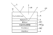
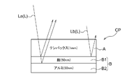
- the radiation cooling device CP includes an infrared radiation layer A that radiates infrared light IR from the radiation surface H, and a side opposite to the side where the radiation surface H is present in the infrared radiation layer A.
- the light reflection layer B to be positioned is provided in a laminated state.
- the light reflecting layer B includes a first layer B1 made of silver or a silver alloy and a second layer B2 made of aluminum (abbreviated as “aluminum” in the following description) or an aluminum alloy (abbreviated as “aluminum alloy” in the following description).
- an alloying-preventing transparent layer B3 for preventing alloying of silver and aluminum are positioned on the side closer to the infrared radiation layer A in the order of the first layer B1, the alloying-preventing transparent layer B3, and the second layer B2. It is comprised in the state laminated
- the thickness (film thickness) of the first layer B1 is configured to be larger than 3.3 nm and 100 nm or less, and preferably the thickness (film thickness) of the first layer B1 is configured to be 50 nm or more and 100 nm or less. Has been.
- the thickness (film thickness) of the second layer B2 is configured to be 10 nm or more.
- the “silver alloy” an alloy in which any of copper, palladium, gold, zinc, tin, magnesium, nickel and titanium is added to silver, for example, about 0.4 to 4.5 mass% is used. Can do.
- APC-TR made by Furuya Metal
- the first layer B1 is made of silver.
- the “aluminum alloy” an alloy obtained by adding copper, manganese, silicon, magnesium, zinc, carbon steel for mechanical structure, yttrium, lanthanum, gadolinium, and terbium to aluminum can be used. In the following description, it is assumed that the second layer B2 is made of aluminum.
- the alloying-preventing transparent layer B3 is composed of a transparent nitride film or a transparent oxide film.
- the transparent nitride film include Si 3 N 4 and AlN.
- the transparent oxide film include Al 2 O 3 , SiO 2 , TiO 2 , ZrO 2 , HfO 2 , Nb 2 O 5 , Ta 2 O 5 , and other oxides that can be easily formed by vapor deposition or sputtering. The details will be described later.
- the thickness of the alloying-preventing transparent layer B3 is such that any one of the wavelengths of 400 nm or less is a resonance wavelength, and preferably any one of the wavelengths of 300 nm or less is the resonance wavelength. The details will be described later.
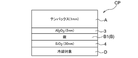
- the radiant cooling device CP is configured by laminating the first layer B1, the alloying-preventing transparent layer B3, and the second layer B2 using the infrared radiation layer A as a substrate. Specifically, the adhesion layer 3 is laminated between the infrared radiation layer A as the substrate and the first layer B1, and the opposite side of the second layer B2 from the existence side of the anti-alloying transparent layer B3. In addition, an antioxidant layer 4 is laminated.
- the radiant cooling device CP sequentially forms the adhesion layer 3, the first layer B1, the alloying prevention transparent layer B3, the second layer B2, and the antioxidant layer 4 by, for example, sputtering using the infrared radiation layer A as a substrate. It is comprised in the form to do.
- the adhesion layer 3 is configured to form aluminum oxide (Al 2 O 3 ) to a thickness of 20 to 100 nm.
- the antioxidant layer 4 is configured to form silicon dioxide (SiO 2 ) or aluminum oxide (Al 2 O 3 ) to a thickness of 10 to several 100 nm. In the following description, it is assumed that silicon dioxide (SiO 2 ) is formed.
- the infrared radiation layer A is made of any one of alkali-free glass, crown glass, and borosilicate glass (white plate glass).
- alkali-free glass for example, OA10G (manufactured by Nippon Electric Glass) can be used
- crown glass for example, B270 (registered trademark, the same shall apply hereinafter)
- borosilicate glass for example, Tempax (registered trademark, hereinafter the same) can be used.
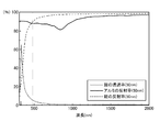
- “OA10G”, “B270”, and “Tempax” have high transmittance with respect to light having a wavelength corresponding to sunlight as shown in FIG. 8, and also have high atmospheric transmittance as shown in FIG. The emissivity of the wavelength corresponding to the wavelength range (so-called atmospheric window) is high.
- FIG. 8 exemplifies “Tempax” as a representative, but “OA10G”, “B270”, etc. of white plate glass are the same. In the following description, it is assumed that the infrared radiation layer A is formed of “Tempax”.
- the radiant cooling device CP reflects a part of the light L incident on the radiant cooling device CP (for example, a part of sunlight) on the radiation surface H of the infrared radiation layer A.
- the light (ultraviolet light, etc.) transmitted through the infrared radiation layer A among the light L incident on the radiation cooling device CP is reflected by the light reflection layer B.
- heat input to the radiation cooling device CP from the cooling object D located on the side opposite to the side where the light reflection layer B is present in the antioxidant layer 4 (for example, heat input from the cooling object D by heat conduction) is converted into red.
- the cooling target D is cooled by being converted into infrared light IR by the outer radiation layer A and radiating.
- light means an electromagnetic wave having a wavelength of 10 nm to 20000 nm. That is, the light L includes ultraviolet light, infrared light IR, and visible light.
- the radiation cooling device CP is formed by forming an infrared radiation layer A with a Tempax having a thickness of 1 mm, a first layer B1 of the light reflection layer B having a thickness of 50 nm, and reflecting light.
- the second layer B2 of the layer B is made of aluminum with a film thickness of 50 nm
- the adhesion layer 3 is formed with aluminum oxide (Al 2 O 3 ) with a film thickness of 5 nm
- silicon dioxide (SiO 2 ) with a film thickness of 30 nm is formed.
- the oxidation preventing layer 4 is formed and the alloying prevention transparent layer B3 of the light reflecting layer B is composed of Si 3 N 4 as a transparent nitride film or Al 2 O 3 as a transparent oxide film
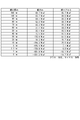
- the cooling capacity of the radiant cooling device CP was calculated while changing the thickness of Si 3 N 4 as the transparent nitride film and Al 2 O 3 as the transparent oxide film, and the results shown in the tables of FIGS. 3 and 4 were obtained. became.
- the tables in FIG. 3 and FIG. 4 were calculated using a clear day in Osaka in late August as a model. That is, the solar energy is 1000 W / m 2 , the outside air temperature is 30 ° C., and the atmospheric radiation energy is 387 W / m 2 , which is calculated in late August as a model. This is calculated assuming that the temperature of the surface of the layer 4 on the side opposite to the side where the light reflecting layer B is present: hereinafter referred to as the cooling surface temperature) is 30 ° C.
- the thickness (film thickness) of Si 3 N 4 is best at 34 nm or less, and may be 47 nm or less. The reason will be described later.
- the thickness (film thickness) of Al 2 O 3 is best at 44 nm or less, and may be 60 nm or less. The reason will be described later.
- the table in FIG. 7 was calculated using a clear day in Osaka in late August as a model. That is, the solar energy is 1000 W / m 2 , the outside air temperature is 30 ° C., and the atmospheric radiation energy is 387 W / m 2 , which is calculated in late August as a model. The temperature was calculated as 30 ° C. Note that the cooling capacity in FIG. 7 is calculated assuming that the alloying-preventing transparent layer B3 does not exist.
- the radiation cooling device CP when the light reflection layer B is composed only of the first layer B1 (see FIG. 5), when the thickness of the silver forming the first layer B1 is 30 nm or less, the radiation cooling device CP However, when the light reflecting layer B is composed of the first layer B1 and the second layer B2 (see FIG. 6), if the thickness of silver is larger than 3.3 nm, The radiant cooling device CP has a cooling capacity.
- the light reflecting layer B is composed of the first layer B1 and the second layer B2 (see FIG. 6)
- the cooling capacity of the radiation cooling device CP is light reflecting.
- the layer B is composed of only the first layer B1 (see FIG. 5)
- the same ability is obtained when the silver thickness is 300 nm.
- the thickness of the Tempax constituting the infrared radiation layer A needs to be 10 ⁇ m or more and 10 cm or less, preferably 20 ⁇ m or more and 10 cm or less, more preferably 100 ⁇ m or more and 1 cm or less. That is, the infrared radiation layer A exhibits a large thermal radiation in the infrared region having a wavelength of 8 ⁇ m or more and 14 ⁇ m or less, and the thermal radiation is absorbed by each of the infrared radiation layer A and the light reflection layer B. By making it larger than sunlight and the thermal radiation of the atmosphere, it is possible to configure a radiant cooling device CP that exhibits a radiative cooling action in which the temperature is lower than the surrounding atmosphere regardless of day or night.
- the thickness must be 10 ⁇ m or more and 10 cm or less, preferably 20 ⁇ m or more and 10 cm or less, more preferably 100 ⁇ m or more and 1 cm or less are preferable.
- the cooling capacity of the radiation cooling device CP is improved, but in a state where silver and aluminum are kept in contact with each other.
- the alloying of silver and aluminum progresses, the reflectance of sunlight decreases, and the absorption of sunlight increases. Therefore, between the first layer B1 and the second layer B2 By positioning the alloying preventing transparent layer B3, alloying of silver and aluminum is suppressed.
- the anti-alloying transparent layer B3 When the anti-alloying transparent layer B3 is positioned between the first layer B1 and the second layer B2, the reflectance of sunlight in the light reflecting layer B is slightly lowered and the absorption of sunlight is slightly increased. Therefore, as shown in FIGS. 3 and 4, when the thickness of Si 3 N 4 as a transparent nitride film and Al 2 O 3 as a transparent oxide film is set to 0 nm, that is, an alloying-preventing transparent layer Compared to the case without B3, the cooling capacity of the radiation cooling device CP is slightly reduced, but the alloying of silver and aluminum is suppressed, and the reflection performance of the light reflection layer B is maintained over a long period of time. It will be possible.
- the light reflection layer B of the radiation cooling device CP is provided with the first layer B1 and the second layer B2.
- the light reflection layer B of the radiation cooling device CP is composed only of the first layer B1 made of silver having a thickness of 50 nm, as shown in FIG. The light passes through the 50 nm silver constituting the first layer B1, and the transmitted light is irradiated to the cooling object D.
- the cooling object D is configured as a light absorption layer or a heat exchanger in order to efficiently release the heat of the object to be cooled, but the thickness (thickness) of the silver constituting the first layer B1 is reduced. Then, since the transmitted light warms the cooling object D, the radiation cooling capacity (radiation cooling performance) is weakened.
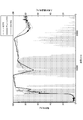
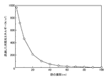
- FIG. 13 shows the film thickness (thickness) of silver and the energy of sunlight (W / m) in the radiation cooling device CP (see FIG. 10) in which the light reflecting layer B is composed of the first layer B1 made of silver. 2 ).
- the radiation cooling capacity of the conventional radiant cooling device CP in which the film thickness (thickness) of the silver constituting the first layer B1 is 300 nm is as follows: summer in Japan, altitude 0m, outside temperature 30 ° C It is approximately 70 W / m 2 , depending on the humidity and the air quality during the south-west.
- the film thickness (thickness) of the silver constituting the first layer B1 is 100 nm
- the energy of transmitted sunlight becomes about 7 W / m 2
- this transmitted light heats the cooling target D.
- the cooling capacity of the radiation cooling device CP is reduced by about 10%.
- the film thickness (thickness) of the silver constituting the first layer B1 is 50 nm
- the energy of transmitted sunlight becomes about 70 W / m 2
- the transmitted light is radiated by heating the cooling object D.
- the radiation cooling capacity of the cooling device CP is greatly reduced.
- the film thickness (thickness) of the silver constituting the first layer B1 is reduced.
- the problem that occurred was explained. That is, in the case where the light reflecting layer B is constituted by only the first layer B1, the film thickness (thickness) of the silver constituting the first layer B1 cannot be sufficiently reduced.
- film thickness (thickness) As shown in FIG. 16, if aluminum has a film thickness (thickness) of 25 nm or more, it can shield sunlight transmission accurately. However, as shown in FIG. 15, aluminum tends to have a higher absorption rate of sunlight, and as shown in FIG. 17, aluminum (film thickness 50 nm) emits sunlight more than silver (film thickness 300 nm). It absorbs a lot.
- the problem in the case where the light reflecting layer B is constituted only by the second layer B2 has been described with reference to FIGS. That is, it can be seen that when the light reflection layer B is configured only by the second layer B2, the radiation cooling capacity of the radiation cooling device CP cannot be made sufficient.
- the present inventor has found that if the light reflection layer B of the radiation cooling device CP is constituted by the first layer B1 and the second layer B2, the film thickness (thickness) of the silver constituting the first layer B1. It has been found that the radiation cooling capacity can be made sufficient while the thickness is reduced.
- the transmittance of silver constituting the first layer B1 increases as the wavelength decreases, and increases as the film thickness (thickness) decreases.
- the reflectance of silver constituting the first layer B1 is larger on the long wavelength side, smaller on the shorter wavelength side, and smaller as the film thickness (thickness) becomes thinner.
- the aluminum of the second layer B2 is provided with a large reflectance enough to shield sunlight transmission as long as it has a film thickness (thickness) of 25 nm or more.
- the reflectance tends to be smaller than that of silver.
- crossing wavelength the wavelength at which the reflectance of silver and the reflectance of aluminum intersect (hereinafter, abbreviated as “crossing wavelength”) varies depending on the film thickness (thickness) of silver.
- FIG. 22 illustrates cross wavelengths when the film thickness (thickness) of aluminum is changed when the film thickness (thickness) of aluminum is 200 nm.
- the film thickness (thickness) of silver constituting the first layer B1 is 50 nm.
- the cross wavelength is 450 nm, and in the light La on the shorter wavelength side than 450 nm, aluminum is more silver than silver.
- the reflectance of silver is higher than that of aluminum in light Lb on the longer wavelength side.
- light having a wavelength of 450 nm or less, which is an intersecting wavelength easily transmits silver, and thus the transmitted light is irradiated to the aluminum of the second layer B2.
- the light La having a wavelength shorter than 450 nm is reflected by the first layer B1 partially formed of silver, and the light transmitted through the first layer B1 is formed of aluminum. It is reflected by the second layer B2. Further, the light Lb having a wavelength longer than 450 nm is mainly reflected by the first layer B1.
- the light reflecting layer B is composed of the first layer B1 and the second layer B2
- the film thickness (thickness) of the aluminum constituting the second layer B2 is greater than 10 nm. Since it does not transmit, the film thickness (thickness) of the second layer B2 is 10 nm or more.
- the thickness (thickness) of the aluminum constituting the second layer B2 is increased to 50 nm or more. That is, aluminum is oxidized to form a passive state, but the durability increases as the layer capable of forming the passive state becomes thicker.
- the film thickness (thickness) of the silver of the first layer B1 is 50 nm
- the aluminum of B2 By reflecting with the aluminum of B2, the light transmitted through the infrared radiation layer A can be efficiently reflected.
- the light reflecting layer B is composed of the first layer B1 and the second layer B2
- the light having a wavelength longer than the crossing wavelength is reflected mainly by the silver of the first layer B1, and the silver is reflected.
- the light transmitted through the infrared radiation layer A can be efficiently reflected.
- the film thickness (thickness) of the first layer B1 is 100 nm or less and 50 nm or more, The reflectance of sunlight can be sufficiently improved.
- the radiation cooling device CP will produce a radiant cooling capability (radiant cooling performance).
- the radiation cooling capacity (radiation cooling performance) of the radiation cooling device CP is such that the light reflection layer B is composed of only the first layer B1 ( In FIG. 2), the same ability is obtained when the silver thickness is 300 nm.
- the light reflection layer B of the radiation cooling device of the present invention is made of a noble metal by reflecting light in the visible light region from the ultraviolet light that passes through the silver of the first layer B1 with the aluminum of the second layer B2. It reduces the amount of silver used. For this reason, the light transmitted through the silver of the first layer B1 needs to be transmitted as much as possible through the transparent nitride film and the transparent oxide film constituting the alloying-preventing transparent layer B3.
- the transparent nitride film and transparent oxide film constituting the alloying prevention transparent layer B3 need to be transparent in the ultraviolet to visible light region, but what kind of transparent nitride film and transparent oxide film are suitable?
- narrow down from the viewpoint of chemical reactivity it is preferable to screen with reference to the standard production Gibbs energy.
- the reaction of the following formula (1) in which the metal A and oxygen react proceeds in the direction in which the standard production Gibbs energy is small.
- the standard production Gibbs energy is smaller in the reaction of the following formula (2) than the reaction of the above formula (1).
- the oxide film semi-permanently highly transparent select a material with a standard Gibbs energy of transparent nitride film and transparent oxide film that is smaller than that of silver or aluminum as the material for transparent nitride film or transparent oxide film. It is important to do.
- the material of the transparent oxide film there is no problem even if a material higher than the standard generation energy of aluminum is selected because of the low oxygen diffusibility of aluminum.
- a material higher than the standard generation energy of aluminum is selected because of the low oxygen diffusibility of aluminum.
- a transparent nitride film a material whose standard generation Gibbs energy is equal to or less than silver and aluminum may be selected. That is, since Ag 3 N (+315 kJ / mol) and AlN ( ⁇ 287 kJ / mol), a material smaller than ⁇ 287 kJ / mol of Al is preferable, and a material transparent in the ultraviolet to visible region is desired. Specific examples of materials that satisfy such conditions include Si 3 N 4 ( ⁇ 676 kJ / mol) and AlN ( ⁇ 287 kJ / mol).
- a material whose standard generation Gibbs energy change is equal to or less than silver may be selected. That is, since it is Ag 2 O ( ⁇ 11 kJ / mol), it is preferable to select a material whose standard production Gibbs energy is smaller than ⁇ 11 kJ / mol.
- the transparent oxide film there is no problem even if a material larger than the standard production Gibbs energy ( ⁇ 1582 kJ / mol) of the aluminum oxide Al 2 O 3 is used. The reason is that Al 2 O 3 is a material having an extremely low oxygen diffusibility. A specific example will be described.
- Group 1 element oxides Li 2 O ( ⁇ 561 kJ / mol), Na 2 O ( ⁇ 375 kJ / mol), K 2 O ( ⁇ 320 kJ / mol)
- Group 2 element oxides BeO (-580 kJ / mol), MgO (-569 kJ / mol), CaO (-604 kJ / mol), SrO (-592 kJ / mol), BaO (-520 kJ / mol)
- Group 4 element oxides TiO 2 ( ⁇ 884 kJ / mol), ZrO 2 ( ⁇ 1042 kJ / mol), HfO 2 ( ⁇ 1088 kJ / mol)
- Group 5 element oxides Nb 2 O 5 ( ⁇ 1766 kJ / mol), Ta 2 O 5 ( ⁇ 1911 kJ / mol)
- Group 13 element oxides B 2 O 3 ( ⁇ 1194 kJ / mol), Al 2 O 3 ( ⁇ 1582 kJ / mol
- Al 2 O 3 ( ⁇ 1582 kJ / mol), SiO 2 ( ⁇ 856 kJ / mol), TiO 2 ( ⁇ 884 kJ / mol), ZrO 2 ( ⁇ 1042 kJ / mol) , HfO 2 ( ⁇ 1088 kJ / mol), Nb 2 O 5 ( ⁇ 1766 kJ / mol), Ta 2 O 5 ( ⁇ 1911 kJ / mol), and these materials are easy to form.
- the transparent oxide film may be Al 2 O 3 which is an oxide of Al, Nb 2 O 5 ( ⁇ 1766 kJ / mol), Ta 2 O 5 ( ⁇ 1911 kJ / mol) should be selected. In this case, the change in reflectance over time due to the reaction between Al and the transparent oxide film does not occur.
- the standard production Gibbs energy of Ag 3 N is +315 kJ / mol
- the standard production Gibbs energy of Ag 2 O is ⁇ 11 kJ / mol. That is, Ag 3 N having a positive standard Gibbs energy is very unstable, and it is more stable if Ag and N 2 exist separately.
- Ag 2 O having a negative standard generation Gibbs energy is more stable when it becomes black silver oxide than when it is divided into Ag and O 2 .
- the alloying-preventing transparent layer B3 is a transparent oxide film.
- the alloying prevention transparent layer B3 is used as a transparent oxide film
- silver is formed between the first layer B1 and the alloying prevention transparent layer B3 when the transparent oxide film is formed.
- Oxidized silver oxide E may be formed in a film shape.
- Al 2 O 3 is formed from the viewpoint of the standard generation Gibbs energy.
- sputtering is a technique in which radicalized gas in plasma is applied as kinetic energy to a target material, and the material knocked out thereby is laminated on a sample. Further, when forming an oxide film, it is common to form a film with a gas in which oxygen is introduced into plasma to produce oxygen radicals.
- oxides such as Al 2 O 3 and SiO 2 generally have a very low film formation rate
- a sputtering rate such as Al or Si is high, a target before oxidation is knocked out, and a large amount of oxygen is put into the plasma.
- a method is used in which an oxide is produced by reacting oxygen and a target material on the sample surface. This method is called “reactive sputtering”.
- a transparent nitride film is more suitable than the transparent oxide film as the alloying-preventing transparent layer B3. This is because silver discoloration can be prevented even if a film is formed under complicated conditions not limited by sputtering or vapor deposition (even if productivity is improved).
- Ag 3 N (+315 kJ / mol) is very unstable, and it is more stable if Ag and N 2 are present.
- silver nitride (black) cannot be formed in the first place with the energy of sputtering or vapor deposition regardless of the conditions. Therefore, when a transparent nitride film is used as the anti-alloying transparent layer B3, variations in film formation become extremely rich. Therefore, it is considered preferable to use a transparent nitride film as the anti-alloying transparent layer B3.
- the thickness (film thickness) of the alloying-preventing transparent layer B3 is preferably a thickness having any one of wavelengths of 400 nm or less as a resonance wavelength, and further, of the wavelength of 300 nm or less. It can be considered that a thickness having any one of the wavelengths as the resonance wavelength is more preferable.
- the plasmon resonance wavelength is accurately determined by the refractive index distribution of the silver of the first layer B1, the aluminum of the anti-alloying transparent layer B3, and the aluminum of the second layer B2, but is approximated by the following equation (3).
- ⁇ L * 4 * n / m -------- (3)
- ⁇ is a resonance wavelength
- L is a film thickness
- n is a refractive index at a calculation wavelength
- m is an arbitrary natural number.
- the sunlight spectrum is approximately in the wavelength range of 300 to 4000 nm.
- L ⁇ / (4 * n) 400 / n 400 nm / 4 ------- (4)
- n 400 nm is a refractive index when the wavelength is 400 nm.
- the transparent nitride film is silicon nitride (Si 2 N 3 ).
- the radiation cooling device CP is formed by forming an infrared radiation layer A with Tempax having a thickness of 1 mm, the first layer B1 of the light reflection layer B being silver having a thickness of 50 nm, and reflecting light.
- the second layer B2 of the layer B is made of aluminum with a film thickness of 50 nm
- the adhesion layer 3 is formed with aluminum oxide (Al 2 O 3 ) with a film thickness of 5 nm
- silicon dioxide (SiO 2 ) with a film thickness of 30 nm is formed.
- the anti-oxidation layer 4 is formed and the light reflection layer B is configured to include the anti-alloying transparent layer B3 (see FIG. 2), Si 3 N 4 as a transparent nitride film or a transparent oxide film when changing the thickness of the Al 2 O 3 as a diagram showing the reflectance of the light reflecting layer B.
- the transparent oxide film has a refractive index greatly different from that of the transparent nitride film.
- n 400 nm is 1.67 and n 300 nm is 1.70. Therefore, when the resonance wavelength is calculated, as shown in FIG. 24, when the transparent oxide film is aluminum oxide (Al 2 O 3 ), the film thickness is preferably 60 nm or less, and particularly preferably 44 nm or less. In view of preventing the peeling due to the shear stress due to the difference in the coefficient of thermal expansion of the material, the thinner (thickness) of the alloying prevention transparent layer B3 is better.
- the film thickness (thickness) when the first layer B1 is formed of a silver alloy is the first layer B1.
- the film thickness (thickness) when the second layer B2 is formed of an aluminum alloy is the second layer B2. Can be made equal to the film thickness (thickness) in the case of forming aluminum.
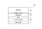
- Adhesion layer 4 Antioxidation layer A Infrared radiation layer B Light reflection layer B1 First layer B2 Second layer B3 Anti-alloying transparent layer
Abstract
光反射層の低廉化を図りながらも、冷却対象を適切に冷却でき、しかも、長期間に亘って冷却作用を良好に発揮できる放射冷却装置を提供する。 放射面Hから赤外光IRを放射する赤外放射層Aと、当該赤外放射層Aにおける放射面Hの存在側とは反対側に位置させる光反射層Bとが積層状態で設けられ、光反射層Bが、銀あるいは銀合金からなる第1層B1と、アルミニウムあるいはアルミニウム合金からなる第2層B2と、銀とアルミニウムとの合金化を防止する合金化防止透明層B3とを、第1層B1、合金化防止透明層B3及び第2層B2の順に赤外放射層Aに近い側に位置させる形態で積層した状態に構成されている。
Description
本発明は、放射面から赤外光を放射する赤外放射層と、当該赤外放射層における前記放射面の存在側とは反対側に位置させる光反射層とが積層状態で設けられた放射冷却装置に関する。
かかる放射冷却装置は、赤外放射層の放射面から放射される赤外光を大気の窓(例えば、波長が8~13μmの赤外光を透過させる窓等)を通して透過させて、光反射層における赤外放射層の存在側とは反対側に位置する冷却対象を冷却する等、各種の冷却対象の冷却に用いられるものである。
ちなみに、光反射層は、赤外放射層を透過した光(可視光、紫外光、赤外光)を反射して放射面から放射させることにより、赤外放射層を透過した光(可視光、紫外光、赤外光)が冷却対象に投射されて、冷却対象が加温されることを回避することになる。
尚、光反射層は、赤外放射層を透過した光に加えて、赤外放射層から光反射層の存在側に放射される赤外光を赤外放射層に向けて反射する作用も有することになるが、以下の説明においては、光反射層が、赤外放射層を透過した光(可視光、紫外光、赤外光)を反射するために設けられるものであるとして説明する。
尚、光反射層は、赤外放射層を透過した光に加えて、赤外放射層から光反射層の存在側に放射される赤外光を赤外放射層に向けて反射する作用も有することになるが、以下の説明においては、光反射層が、赤外放射層を透過した光(可視光、紫外光、赤外光)を反射するために設けられるものであるとして説明する。
このような放射冷却装置の第1の従来例として、光反射層が、銀からなる金属層と、二酸化チタン(TiO2)の層とフッ化マグネシウム(MgF2)の層とを交互に並べる状態で多層状態に形成したフォトニング・バンドキャップ層とを、フォトニング・バンドキャップ層を赤外放射層に近い側に位置させる形態で積層した状態に構成されたものがある(例えば、特許文献1参照。)。
また、放射冷却装置の第2の従来例として、光反射層が、アルミニウムからなる金属層として構成されたものがある(例えば、特許文献2参照。)。
ちなみに、特許文献2には、アルミニウムからなる金属層を基板として、赤外放射層を構成するSiO層とMgO層とを積層するように構成されている。
ちなみに、特許文献2には、アルミニウムからなる金属層を基板として、赤外放射層を構成するSiO層とMgO層とを積層するように構成されている。
第1の従来例においては、光反射層が、多層状態に積層されるフォトニング・バンドキャップ層を備えるものであるため、製作が煩雑となる不利があり、しかも、フォトニング・バンドキャップ層を備えるにしても、高価な銀からなる金属層を十分に薄くできないため、全体構成の低廉化を図り難い不利があった。
第2の従来例においては、光反射層が、アルミニウムからなる金属層として構成されるものであるから、安価なアルミニウムにて光反射層が構成されるため、全体構成の低廉化を図れるものである。
しかしながら、アルミニウムからなる金属層は、銀よりも光を吸収し易いものであるから、赤外放射層を透過した光が、アルミニウムからなる金属層に吸収されて、当該光の吸収により昇温する金属層が、冷却対象を加温すること等に起因して、冷却対象を適切に冷却できない虞があった。
しかしながら、アルミニウムからなる金属層は、銀よりも光を吸収し易いものであるから、赤外放射層を透過した光が、アルミニウムからなる金属層に吸収されて、当該光の吸収により昇温する金属層が、冷却対象を加温すること等に起因して、冷却対象を適切に冷却できない虞があった。
このような状況に鑑みて、本発明の発明者が鋭意研究した結果によれば、光反射層を、厚さが100nm以上の銀からなる金属層として構成すれば、赤外放射層を透過した光が冷却対象に投射されることを抑制しながら、冷却対象を冷却することができるものとなり(図12、図13参照)、そして、光反射層を、厚さが300nm以上の銀からなる金属層として構成すれば、赤外放射層を透過した光が冷却対象に投射されることを的確に抑制して、冷却対象を適切に冷却できることが判明した。
しかしながら、銀は高価な金属であるから、光反射層を、厚さが300nm以上の銀からなる金属層として構成すれば、放射冷却装置が高価となるものとなるため、銀の使用量を極力抑制しながら、冷却対象を冷却することが望まれるものであった。
本発明は、上記実情に鑑みて為されたものであって、その目的は、光反射層の低廉化を図りながらも、冷却対象を適切に冷却でき、しかも、長期間に亘って冷却作用を良好に発揮できる放射冷却装置を提供する点にある。
本発明の放射冷却装置は、放射面から赤外光を放射する赤外放射層と、当該赤外放射層における前記放射面の存在側とは反対側に位置させる光反射層とが積層状態で設けられたものであって、その特徴構成は、
前記光反射層が、銀あるいは銀合金からなる第1層と、アルミニウムあるいはアルミニウム合金からなる第2層と、銀とアルミニウムとの合金化を防止する合金化防止透明層とを、前記第1層、前記合金化防止透明層及び前記第2層の順に前記赤外放射層に近い側に位置させる形態で積層した状態に構成されている点にある。
前記光反射層が、銀あるいは銀合金からなる第1層と、アルミニウムあるいはアルミニウム合金からなる第2層と、銀とアルミニウムとの合金化を防止する合金化防止透明層とを、前記第1層、前記合金化防止透明層及び前記第2層の順に前記赤外放射層に近い側に位置させる形態で積層した状態に構成されている点にある。
すなわち、本発明の発明者が鋭意研究した結果、光反射層を、銀あるいは銀合金からなる第1層とアルミニウムあるいはアルミニウム合金からなる第2層とを、第1層を赤外放射層に近い側に位置させる形態で積層した状態に構成することにより、高価な銀あるいは銀合金の使用量を抑制しながら、冷却対象を冷却できることを見出すに至った。
つまり、銀あるいは銀合金は、可視光や赤外光を効率良く反射できるものの、紫外光の反射率が低い傾向となる。
これに対して、アルミニウムあるいはアルミニウム合金は、銀あるいは銀合金に較べて、可視光や赤外光を効率良く反射することができないものの、紫外光を効率良く反射することができる傾向となる。
しかも、アルミニウムあるいはアルミニウム合金は、銀あるいは銀合金に較べて、可視光や赤外光を吸収し易い傾向となる。
これに対して、アルミニウムあるいはアルミニウム合金は、銀あるいは銀合金に較べて、可視光や赤外光を効率良く反射することができないものの、紫外光を効率良く反射することができる傾向となる。
しかも、アルミニウムあるいはアルミニウム合金は、銀あるいは銀合金に較べて、可視光や赤外光を吸収し易い傾向となる。
そこで、銀あるいは銀合金からなる第1層とアルミニウムあるいはアルミニウム合金からなる第2層とを、第1層を赤外放射層に近い側に位置させる形態で積層した状態に構成することにより、第1層が可視光や赤外光を反射することにより、第2層が可視光や赤外光を吸収することを抑制し、しかも、第1層の厚さを薄くしても、第1層及び第2層の存在により、赤外放射層を透過した光(可視光、紫外光、赤外光)を適切に反射して、冷却対象を冷却できることを見出すに至ったのである。
そして、銀あるいは銀合金からなる第1層を薄くできるため、光反射層の低廉化を図ることができるのである。
さらに、第1層と第2層との間には、銀とアルミニウムとの合金化を防止する合金化防止透明層を設けるものであるから、銀とアルミニウムとが合金化することを抑制できるため、光反射層の光の吸収を回避しながら、光反射層により光を適切に反射する状態を長期間に亘って維持させて、長期間に亘って冷却作用を良好に発揮させることができる。
つまり、第1層の銀あるいは銀合金と第2層のアルミニウムあるいはアルミニウム合金とを接触させた状態で長時間経過すると、銀とアルミニウムの合金化が次第に進み、光反射層の太陽光の反射率が悪くなり、太陽光吸収が増加することが予想されるため、銀とアルミの合金化を防止するために、第1層と第2層との間に合金化防止透明層を設けることによって、銀とアルミの合金化を抑制するのである。
要するに、本発明の放射冷却装置によれば、光反射層の低廉化を図りながらも、冷却対象を適切に冷却でき、しかも、長期間に亘って冷却作用を良好に発揮できる。
本発明の放射冷却装置の更なる特徴構成は、前記第1層の厚さが、3.3nmよりも大きく、かつ、100nm以下である点にある。
すなわち、銀あるいは銀合金からなる第1層の厚さを、3.3nmよりも大きく、かつ、100nm以下である範囲で変化させても、第2層の存在により、赤外放射層を透過した光(可視光、紫外光、赤外光)を適切に反射して、冷却対象を冷却できることが判明した。
つまり、銀あるいは銀合金からなる第1層の厚さを、3.3nmよりも大きく、かつ、100nm以下である範囲の薄い厚さにして、光反射層の低廉化を十分に図りながらも、冷却対象を冷却できる。
但し、銀あるいは銀合金からなる第1層の厚さを、3.3nmよりも大きく、かつ、100nm以下である範囲の間において、好ましくは、30nm以上に大きくすることにより、冷却対象を適切に冷却できることになる。
要するに、本発明の放射冷却装置の更なる特徴構成によれば、光反射層の低廉化を十分に図りながらも、冷却対象を冷却できる。
本発明の放射冷却装置の更なる特徴構成は、前記第1層の厚さが、50nm以上100nm以下である点にある。
すなわち、銀あるいは銀合金からなる第1層の厚さを、50nm以上100nm以下の範囲にすれば、第1層による光(主として、可視光、赤外光)の反射作用を適切に発揮させながら、第2層の存在により、赤外放射層を透過した光(可視光、紫外光、赤外光)を適切に反射することができる結果、光反射層を、厚さが300nm以上の銀からなる金属層として構成する場合と同等の能力にて、冷却対象を冷却できることを見出すに至った。
従って、第1層の厚さを薄くして、光反射層の低廉化を図りながらも、厚さが300nm以上の銀からなる金属層として構成する場合と同等の大きな冷却能力を得ることができる。
要するに、本発明の放射冷却装置の更なる特徴構成によれば、光反射層の低廉化を図りながらも、大きな冷却能力を得ることができる。
本発明の放射冷却装置の更なる特徴構成は、前記第2層の厚さが、10nm以上である点にある。
すなわち、光反射層を第1層と第2層とから構成する場合には、アルミニウムあるいはアルミニウム合金からなる第2層の厚さが、10nm以上であれば、第2層が紫外光を反射する作用を適切に発揮させて、第1層との組み合わせにより、赤外放射層を透過した光(可視光、紫外光、赤外光)を適切に反射することができることを見出すに至った。
ちなみに、アルミニウムあるいはアルミニウム合金からなる第2層の厚さは、10nm以上であればよいが、アルミニウムあるいはアルミニウム合金の使用量を抑制するためには、必要以上に厚くすることは避ける必要がある。
要するに、本発明の放射冷却装置の更なる特徴構成によれば、紫外光を反射する作用を適切に発揮させながら、赤外放射層を透過した光を反射することができる。
本発明の放射冷却装置の更なる特徴構成は、前記赤外放射層が、無アルカリガラス、クラウンガラス、ホウケイ酸ガラスのうちのいずれかのガラスにて構成されている点にある。
すなわち、無アルカリガラス、クラウンガラス、ホウケイ酸ガラスは、比較的に安価でありながらも、太陽光(可視光、紫外光、近赤外光)の透過性が優れた(例えば、80%程度を透過する)ものであるため、太陽光を吸収することがなく、しかも、大気の窓(例えば、波長が8~13μmの赤外光を透過させる窓等)に相当する波長の赤外光を放射する輻射強度が高い性質を有する。
したがって、赤外放射層を、無アルカリガラス、クラウンガラス、ホウケイ酸ガラスのうちのいずれかのガラスにて構成することにより、全体構成の低廉化を図りながらも、冷却能力の高い放射冷却装置を得ることができる。
要するに、本発明の放射冷却装置の更なる特徴構成によれば、全体構成の低廉化を図りながらも、冷却能力の向上を得ることができる。
本発明の放射冷却装置の更なる特徴構成は、前記赤外放射層を基板として、前記第1層、前記合金化防止透明層及び前記第2層が積層されている点にある。
すなわち、赤外放射層を基板として、第1層、合金化防止透明層及び第2層が積層されているから、全体構成の簡素化を図り、しかも、全体構成の薄膜化を図ることができる。
ちなみに、赤外放射層を基板として、第1層、合金化防止透明層及び第2層を積層する際に、第1層、合金化防止透明層及び第2層が薄い場合には、例えば、スパッタリング等により、第1層、合金化防止透明層及び第2層を順次積層することになる。
ちなみに、赤外放射層を基板として、第1層、合金化防止透明層及び第2層を積層する際に、第1層、合金化防止透明層及び第2層が薄い場合には、例えば、スパッタリング等により、第1層、合金化防止透明層及び第2層を順次積層することになる。
つまり、積層用基板を設けて、その積層用基板に対して、スパッタリング等により、第2層、合金化防止透明層及び第1層を順次積層し、その後、第1層の第2層の存在側とは反対側箇所に、別途製作した赤外放射層を載置して積層する、又は、第1層の合金化防止透明層の存在側とは反対側箇所に、スパッタリング等により、赤外放射層を積層する場合に較べて、積層用基板を設ける必要が無いため、全体構成の簡素化を図り、しかも、全体構成の薄膜化を図ることができる。
要するに、本発明の放射冷却装置の更なる特徴構成によれば、全体構成の簡素化を図り、しかも、全体構成の薄膜化を図ることができる。
本発明の放射冷却装置の更なる特徴構成は、前記赤外放射層と前記第1層との間に、密着層が積層されている点にある。
すなわち、赤外放射層と光反射層の第1層との間に密着層が積層されているから、温度変化等に起因して、光反射層の第1層が赤外放射層に対して剥離する等の損傷が生じることを抑制できるため、耐久性を向上できる。
要するに、本発明の放射冷却装置の更なる特徴構成によれば、耐久性の向上を図ることができる。
本発明の放射冷却装置の更なる特徴構成は、前記第2層における前記合金化防止透明層の存在側とは反対側に、酸化防止層が積層されている点にある。
すなわち、アルミニウムあるいはアルミニウム合金からなる第2層における合金化防止透明層の存在側とは反対側に、酸化防止層が積層されているから、第2層を薄くしても、第2層が酸化して劣化することを抑制できるため、耐久性を向上できる。
要するに、本発明の放射冷却装置の更なる特徴構成によれば、アルミニウムあるいはアルミニウム合金からなる第2層の劣化を抑制して、耐久性を向上できる。
本発明の放射冷却装置の更なる特徴構成は、前記合金化防止透明層が、透明窒化膜である点にある。
すなわち、合金化防止透明層として、透明窒化膜を設けることにより、第1層の銀あるいは銀合金と第2層のアルミニウムあるいはアルミニウム合金とが合金化することを適切に抑制することができる。
ちなみに、透明窒化膜の具体例としては、Si3N4、AlNを挙げることができる。
尚、透明窒化膜は、スパッタリングや蒸着等を用いて製膜する際に、第1層の銀あるいは銀合金が変色しないため、生産性を向上し易い利点がある。
ちなみに、透明窒化膜の具体例としては、Si3N4、AlNを挙げることができる。
尚、透明窒化膜は、スパッタリングや蒸着等を用いて製膜する際に、第1層の銀あるいは銀合金が変色しないため、生産性を向上し易い利点がある。
要するに、本発明の放射冷却装置の更なる特徴構成によれば、銀とアルミニウムとの合金化を適切に抑制することができる。
本発明の放射冷却装置の更なる特徴構成は、前記合金化防止透明層が、透明酸化膜である点にある。
すなわち、合金化防止透明層として、透明酸化膜を設けることにより、第1層の銀あるいは銀合金と第2層のアルミニウムあるいはアルミニウム合金とが合金化することを適切に抑制することができる。
ちなみに、透明酸化膜としては、多数のものが適用できるが、具体例の一例として、蒸着やスパッタリング等で製膜しやすいAl2O3、SiO2、TiO2、ZrO2、HfO2、Nb2O5、Ta2O5を挙げることができる。
ちなみに、透明酸化膜としては、多数のものが適用できるが、具体例の一例として、蒸着やスパッタリング等で製膜しやすいAl2O3、SiO2、TiO2、ZrO2、HfO2、Nb2O5、Ta2O5を挙げることができる。
要するに、本発明の放射冷却装置の更なる特徴構成によれば、銀とアルミニウムとの合金化を適切に抑制することができる。
本発明の放射冷却装置の更なる特徴構成は、前記合金化防止透明層が、400nm以下の波長のうちのいずれかの波長を共鳴波長とする厚さである点にある。
すなわち、合金化防止透明層は光を吸収することになるが、合金化防止透明層の厚さを、400nm以下の波長のうちのいずれかの波長を共鳴波長とする厚さとすることによって、光反射層全体としての光吸収量を抑制するのである。
つまり、太陽光スペクトルは概ね波長300~4000nmの範囲に存在し、そして、400nmよりも長波長側の太陽光強度(光エネルギー)は強いが、300~400nmの紫外線領域の光は太陽光スペクトルのテールにあたるので、エネルギー的に大きくないものである。
したがって、合金化防止透明層が光を吸収するとしても、400nm以下の短波長側の光を吸収させるようにすることにより、光反射層全体としての光吸収量を抑制できるのである。
したがって、合金化防止透明層が光を吸収するとしても、400nm以下の短波長側の光を吸収させるようにすることにより、光反射層全体としての光吸収量を抑制できるのである。
要するに、本発明の放射冷却装置の更なる特徴構成によれば、光反射層全体としての光吸収量を抑制できる。
本発明の放射冷却装置の更なる特徴構成、前記合金化防止透明層が、300nm以下の波長のうちのいずれかの波長を共鳴波長とする厚さである点にある。
すなわち、合金化防止透明層は光を吸収することになるが、合金化防止透明層の厚さを、300nm以下の波長のうちのいずれかの波長を共鳴波長とする厚さとすることによって、光反射層全体としての光吸収量を適切に抑制するのである。
つまり、太陽光スペクトルは概ね波長300~4000nmの範囲に存在し、そして、400nmよりも長波長側の太陽光強度(光エネルギー)は強いが、300~400nmの紫外線領域の光は太陽光スペクトルのテールにあたるので、エネルギー的には大きくないものであり、さらには、短波長側ほどエネルギー的には小さくなるので、300nm以下になると、エネルギー的には十分に小さいものとなる。
したがって、合金化防止透明層が光を吸収するとしても、300nm以下の短波長側の光を吸収させるようにすることにより、光反射層全体としての光吸収量を適切に抑制できるのである。
したがって、合金化防止透明層が光を吸収するとしても、300nm以下の短波長側の光を吸収させるようにすることにより、光反射層全体としての光吸収量を適切に抑制できるのである。
要するに、本発明の放射冷却装置の更なる特徴構成によれば、光反射層全体としての光吸収量を適切に抑制できる。
以下、本発明の実施形態を図面に基づいて説明する。
〔放射冷却装置の構成〕
図1に示すように、放射冷却装置CPには、放射面Hから赤外光IRを放射する赤外放射層Aと、当該赤外放射層Aにおける放射面Hの存在側とは反対側に位置させる光反射層Bとが積層状態に設けられている。
〔放射冷却装置の構成〕
図1に示すように、放射冷却装置CPには、放射面Hから赤外光IRを放射する赤外放射層Aと、当該赤外放射層Aにおける放射面Hの存在側とは反対側に位置させる光反射層Bとが積層状態に設けられている。
光反射層Bが、銀あるいは銀合金からなる第1層B1とアルミニウム(以下の記載において「アルミ」と略称)あるいはアルミニウム合金(以下の記載において「アルミ合金」と略称)からなる第2層B2と、銀とアルミニウムとの合金化を防止する合金化防止透明層B3とを、第1層B1、合金化防止透明層B3及び第2層B2の順に赤外放射層Aに近い側に位置させる形態で積層した状態に構成されている。
第1層B1の厚さ(膜厚)が、3.3nmよりも大きく且つ100nm以下に構成され、好ましくは、第1層B1の厚さ(膜厚)が、50nm以上で且つ100nm以下に構成されている。
第2層B2の厚さ(膜厚)が、10nm以上に構成されている。
第2層B2の厚さ(膜厚)が、10nm以上に構成されている。
ちなみに、「銀合金」としては、銀に、銅、パラジウム、金、亜鉛、スズ、マグネシウム、ニッケル、チタンのいずれかを、例えば、0.4~4.5質量%程度添加した合金を用いることができる。具体例としては、銀に銅とパラジウムを添加して作成した銀合金である「APC-TR(フルヤ金属製)」を用いることができる。
尚、以下の記載においては、第1層B1を、銀を用いて構成するものとして説明する。
尚、以下の記載においては、第1層B1を、銀を用いて構成するものとして説明する。
「アルミ合金」としては、アルミに、銅、マンガン、ケイ素、マグネシウム、亜鉛、機械構造用炭素鋼、イットリウム、ランタン、ガドリニウム、テルビウムを添加した合金を用いることができる。
尚、以下の記載においては、第2層B2を、アルミを用いて構成するものとして説明する。
尚、以下の記載においては、第2層B2を、アルミを用いて構成するものとして説明する。
合金化防止透明層B3は、透明窒化膜や透明酸化膜にて構成される。
透明窒化膜としては、Si3N4、AlNを挙げることができる。
透明酸化膜としては、蒸着やスパッタリングなどで製膜しやすいAl2O3、SiO2、TiO2、ZrO2、HfO2、Nb2O5、Ta2O5や、その他の酸化物を挙げることができるが、その詳細は後述する。
透明窒化膜としては、Si3N4、AlNを挙げることができる。
透明酸化膜としては、蒸着やスパッタリングなどで製膜しやすいAl2O3、SiO2、TiO2、ZrO2、HfO2、Nb2O5、Ta2O5や、その他の酸化物を挙げることができるが、その詳細は後述する。
合金化防止透明層B3の厚さは、400nm以下の波長のうちのいずれかの波長を共鳴波長とする厚さであり、好ましくは、300nm以下の波長のうちのいずれかの波長を共鳴波長とする厚さであり、その詳細は後述する。
また、放射冷却装置CPは、赤外放射層Aを基板として、第1層B1、合金化防止透明層B3及び第2層B2を積層することにより構成されている。
具体的には、基板としての赤外放射層Aと第1層B1との間に、密着層3が積層され、かつ、第2層B2における合金化防止透明層B3の存在側とは反対側に、酸化防止層4が積層されている。
具体的には、基板としての赤外放射層Aと第1層B1との間に、密着層3が積層され、かつ、第2層B2における合金化防止透明層B3の存在側とは反対側に、酸化防止層4が積層されている。
つまり、放射冷却装置CPが、赤外放射層Aを基板として、例えばスパッタリングにより、密着層3、第1層B1、合金化防止透明層B3、第2層B2及び酸化防止層4を順次製膜する形態に構成されている。
密着層3は、酸化アルミニウム(Al2O3)を20~100nmに製膜する形態に構成されている。
酸化防止層4が、二酸化ケイ素(SiO2)又は酸化アルミニウム(Al2O3)を、10~数100nmに製膜する形態に構成されている。尚、以下の記載においては、二酸化ケイ素(SiO2)が製膜されているとして説明する。
酸化防止層4が、二酸化ケイ素(SiO2)又は酸化アルミニウム(Al2O3)を、10~数100nmに製膜する形態に構成されている。尚、以下の記載においては、二酸化ケイ素(SiO2)が製膜されているとして説明する。
赤外放射層Aが、無アルカリガラス、クラウンガラス、ホウケイ酸ガラスのうちのいずれかのガラス(白板ガラス)にて構成されている。
ちなみに、無アルカリガラスとしては、例えば、OA10G(日本電気硝子製)を用いることができ、クラウンガラスとしては、例えば、B270(登録商標、以下同じ)を用いることができ、ホウケイ酸ガラスとしては、例えば、テンパックス(登録商標、以下同じ)用いることができる。
ちなみに、無アルカリガラスとしては、例えば、OA10G(日本電気硝子製)を用いることができ、クラウンガラスとしては、例えば、B270(登録商標、以下同じ)を用いることができ、ホウケイ酸ガラスとしては、例えば、テンパックス(登録商標、以下同じ)用いることができる。
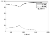
「OA10G」、「B270」及び「テンパックス」は、図8に示すように、太陽光に対応する波長の光に対する透過率が高く、また、図9に示すように、大気の透過率が高い波長域(いわゆる、大気の窓)に相当する波長の輻射率が高い。
ちなみに、図8は「テンパックス」を代表として例示するが、白板ガラスの「OA10G」、「B270」なども同様である。
尚、以下の記載においては、赤外放射層Aが「テンパックス」にて形成されているとして説明する。
ちなみに、図8は「テンパックス」を代表として例示するが、白板ガラスの「OA10G」、「B270」なども同様である。
尚、以下の記載においては、赤外放射層Aが「テンパックス」にて形成されているとして説明する。
従って、放射冷却装置CPは、放射冷却装置CPに入射した光Lのうちの一部の光(例えば、太陽光の一部の光等)を、赤外放射層Aの放射面Hにて反射し、放射冷却装置CPに入射した光Lのうちで赤外放射層Aを透過した光(紫外光等)を、光反射層Bにて反射するように構成されている。
そして、酸化防止層4における光反射層Bの存在側とは反対側に位置する冷却対象Dから放射冷却装置CPへの入熱(例えば、冷却対象Dからの熱伝導による入熱)を、赤外放射層Aによって赤外光IRに変換して放射することにより、冷却対象Dを冷却するように構成されている。
尚、本実施形態において光とは、その波長が10nmから20000nmの電磁波のことを言う。つまり、光Lには、紫外光、赤外光IRおよび可視光が含まれる。
尚、本実施形態において光とは、その波長が10nmから20000nmの電磁波のことを言う。つまり、光Lには、紫外光、赤外光IRおよび可視光が含まれる。
〔放射冷却装置の冷却能力〕
図2に示すように、放射冷却装置CPを、厚さ1mmのテンパックスにて赤外放射層Aを形成し、光反射層Bの第1層B1を膜厚が50nmの銀とし、光反射層Bの第2層B2を膜厚が50nmのアルミとし、密着層3を膜厚が5nmの酸化アルミニウム(Al2O3)にて形成し、膜厚が30nmの二酸化ケイ素(SiO2)にて酸化防止層4を形成し、且つ、光反射層Bの合金化防止透明層B3を、透明窒化膜としてのSi3N4や透明酸化膜としてのAl2O3にて構成する場合において、透明窒化膜としてのSi3N4や透明酸化膜としてのAl2O3の厚さを変化させながら、放射冷却装置CPの冷却能力を計算したところ、図3及び図4の表に示す結果となった。
図2に示すように、放射冷却装置CPを、厚さ1mmのテンパックスにて赤外放射層Aを形成し、光反射層Bの第1層B1を膜厚が50nmの銀とし、光反射層Bの第2層B2を膜厚が50nmのアルミとし、密着層3を膜厚が5nmの酸化アルミニウム(Al2O3)にて形成し、膜厚が30nmの二酸化ケイ素(SiO2)にて酸化防止層4を形成し、且つ、光反射層Bの合金化防止透明層B3を、透明窒化膜としてのSi3N4や透明酸化膜としてのAl2O3にて構成する場合において、透明窒化膜としてのSi3N4や透明酸化膜としてのAl2O3の厚さを変化させながら、放射冷却装置CPの冷却能力を計算したところ、図3及び図4の表に示す結果となった。
図3及び図4の表は、8月下旬の大阪における快晴の日をモデルとして計算した。
すなわち、太陽光エネルギーを1000W/m2とし、外気温を30℃、大気の輻射エネルギーが387W/m2の8月下旬をモデルとして計算したものであって、放射冷却装置CPの温度(酸化防止層4における光反射層Bの存在側とは反対側の面の温度:以下、冷却面温度と記載する場合がある)が30℃であるとして計算したものである。
すなわち、太陽光エネルギーを1000W/m2とし、外気温を30℃、大気の輻射エネルギーが387W/m2の8月下旬をモデルとして計算したものであって、放射冷却装置CPの温度(酸化防止層4における光反射層Bの存在側とは反対側の面の温度:以下、冷却面温度と記載する場合がある)が30℃であるとして計算したものである。
図3に示すように、Si3N4の厚さ(膜厚)は、34nm以下が最もよく、47nm以下でもよい。その理由は後述する。
図4に示すように、Al2O3の厚さ(膜厚)は、44nm以下が最もよく、60nm以下でもよい。その理由は後述する。
図4に示すように、Al2O3の厚さ(膜厚)は、44nm以下が最もよく、60nm以下でもよい。その理由は後述する。
〔放射冷却装置の考察〕
光反射層Bを第1層B1のみにて構成する場合(図5参照)と、光反射層Bを第1層B1及び第2層B2にて構成する場合(図6参照)とにおいて、第1層B1の銀の厚みを変化させながら、放射冷却装置CPの冷却能力を計算したところ、図7の表に示す結果となった。
光反射層Bを第1層B1のみにて構成する場合(図5参照)と、光反射層Bを第1層B1及び第2層B2にて構成する場合(図6参照)とにおいて、第1層B1の銀の厚みを変化させながら、放射冷却装置CPの冷却能力を計算したところ、図7の表に示す結果となった。
図7の表は、8月下旬の大阪における快晴の日をモデルとして計算した。
すなわち、太陽光エネルギーを1000W/m2とし、外気温を30℃、大気の輻射エネルギーが387W/m2の8月下旬をモデルとして計算したものであって、放射冷却装置CPの温度(冷却面温度)が30℃であるとして計算したものである。
尚、図7の冷却能力は、合金化防止透明層B3が存在しないものとして計算したものである。
すなわち、太陽光エネルギーを1000W/m2とし、外気温を30℃、大気の輻射エネルギーが387W/m2の8月下旬をモデルとして計算したものであって、放射冷却装置CPの温度(冷却面温度)が30℃であるとして計算したものである。
尚、図7の冷却能力は、合金化防止透明層B3が存在しないものとして計算したものである。
図7に示すように、光反射層Bを第1層B1のみにて構成する場合(図5参照)には、第1層B1を形成する銀の厚みが30nm以下になると、放射冷却装置CPが冷却能力を生じないものとなるが、光反射層Bを第1層B1及び第2層B2にて構成する場合(図6参照)には、銀の厚みが3.3nmよりも大きいと、放射冷却装置CPが冷却能力を生じるものとなる。
しかも、光反射層Bを第1層B1及び第2層B2にて構成する場合(図6参照)には、銀の厚みが50nm~100nmのときには、放射冷却装置CPの冷却能力が、光反射層Bを第1層B1のみにて構成する場合(図5参照)において銀の厚みを300nmとするときと、同等の能力となる。
ちなみに、赤外放射層Aを構成するテンパックスの厚さは、10μm以上で10cm以下である必要があり、好ましくは、20μm以上で10cm以下、より好ましくは、100μm以上で1cm以下が良い。
つまり、赤外放射層Aを、波長8μm以上14μm以下の赤外域で大きな熱輻射を示し、当該熱輻射が、赤外放射層A及び光反射層Bの夫々にて吸収されるAM1.5Gの太陽光及び大気の熱輻射よりも大きくなるようにすることにより、昼夜を問わず周囲の大気よりも温度が低下する放射冷却作用を発揮する放射冷却装置CPを構成することができる。
そして、そのようにするにあたり、赤外放射層Aをテンパックスにて構成する場合には、厚さを10μm以上で10cm以下にする必要があり、好ましくは、20μm以上で10cm以下、より好ましくは、100μm以上で1cm以下が良い。
つまり、赤外放射層Aを、波長8μm以上14μm以下の赤外域で大きな熱輻射を示し、当該熱輻射が、赤外放射層A及び光反射層Bの夫々にて吸収されるAM1.5Gの太陽光及び大気の熱輻射よりも大きくなるようにすることにより、昼夜を問わず周囲の大気よりも温度が低下する放射冷却作用を発揮する放射冷却装置CPを構成することができる。
そして、そのようにするにあたり、赤外放射層Aをテンパックスにて構成する場合には、厚さを10μm以上で10cm以下にする必要があり、好ましくは、20μm以上で10cm以下、より好ましくは、100μm以上で1cm以下が良い。
このように、光反射層Bを第1層B1及び第2層B2にて構成すると、放射冷却装置CPの冷却能力が向上するものとなるが、銀とアルミとを接触させたままの状態で長時間が経過すると、銀とアルミの合金化が進み、太陽光の反射率が低下して、太陽光の吸収が増加することになるため、第1層B1と第2層B2との間に合金化防止透明層B3を位置させることによって、銀とアルミの合金化を抑制することになる。
そして、第1層B1と第2層B2との間に合金化防止透明層B3を位置させると、光反射層Bにおける太陽光の反射率が少し低下して、太陽光の吸収が少し増加することになるため、図3及び図4に示すように、透明窒化膜としてのSi3N4や透明酸化膜としてのAl2O3の厚さを0nmとした場合、つまり、合金化防止透明層B3が無い場合に較べて、放射冷却装置CPの冷却能力が少し低下することになるが、銀とアルミとの合金化が抑制されて、長期間に亘って光反射層Bの反射性能を維持できるものとなる。
〔第1層及び第2層の補足説明〕
以下、放射冷却装置CPの光反射層Bに、第1層B1と第2層B2とを備えさせる点についての補足説明を行う。
図10に示すように、放射冷却装置CPの光反射層Bを、厚さが50nmの銀からなる第1層B1のみにて構成した場合においては、図11に示すように、短波長側の光が、第1層B1を構成する50nmの銀を透過することになり、透過した光が冷却対象Dに照射されることになる。
以下、放射冷却装置CPの光反射層Bに、第1層B1と第2層B2とを備えさせる点についての補足説明を行う。
図10に示すように、放射冷却装置CPの光反射層Bを、厚さが50nmの銀からなる第1層B1のみにて構成した場合においては、図11に示すように、短波長側の光が、第1層B1を構成する50nmの銀を透過することになり、透過した光が冷却対象Dに照射されることになる。
図12に示すように、銀は、膜厚(厚さ)が薄くなると、薄くなるほど透過率が上昇することになるため、光反射層Bを第1層B1のみにて構成する場合には、銀の膜厚(厚さ)が薄くなるほど、冷却対象Dに照射される光が増加して、放射冷却装置CPの冷却に拘わらず、冷却対象Dの温度が上昇する現象が生じる。
つまり、冷却対象Dは、被冷却物の熱を効率的に逃がすために、光吸収層や熱交換器として構成されるが、第1層B1を構成する銀の膜厚(厚さ)を薄くすると透過した光が冷却対象Dを温めるので放射冷却能力(放射冷却性能)が弱まることになる。
つまり、冷却対象Dは、被冷却物の熱を効率的に逃がすために、光吸収層や熱交換器として構成されるが、第1層B1を構成する銀の膜厚(厚さ)を薄くすると透過した光が冷却対象Dを温めるので放射冷却能力(放射冷却性能)が弱まることになる。
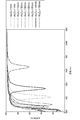
図13は、光反射層Bを銀からなる第1層B1にて構成する放射冷却装置CP(図10参照)において、銀の膜厚(厚さ)と透過する太陽光のエネルギー(W/m2)との関係を示すものである。
第1層B1を構成する銀の膜厚(厚さ)を300nmの膜厚(厚さ)にする従来の放射冷却装置CPの放射冷却能力は、日本の夏、標高0m、外気温度が30℃の南中時、湿度や空気の澄み具合にもよるが、概ね70W/m2程度である。
第1層B1を構成する銀の膜厚(厚さ)を300nmの膜厚(厚さ)にする従来の放射冷却装置CPの放射冷却能力は、日本の夏、標高0m、外気温度が30℃の南中時、湿度や空気の澄み具合にもよるが、概ね70W/m2程度である。
これに対して、第1層B1を構成する銀の膜厚(厚さ)が100nmになると、透過する太陽光のエネルギーが7W/m2程度となり、この透過光が冷却対象Dを加熱することにより、放射冷却装置CPの冷却能力が1割程度低下する。
さらに、第1層B1を構成する銀の膜厚(厚さ)が50nmになると、透過する太陽光のエネルギーが70W/m2程度となり、この透過光が冷却対象Dを加熱することにより、放射冷却装置CPの放射冷却能力が大きく低下する。
さらに、第1層B1を構成する銀の膜厚(厚さ)が50nmになると、透過する太陽光のエネルギーが70W/m2程度となり、この透過光が冷却対象Dを加熱することにより、放射冷却装置CPの放射冷却能力が大きく低下する。
以上の通り、図10~図13に基づいて、光反射層Bを第1層B1のみにて構成する場合において、第1層B1を構成する銀の膜厚(厚さ)を薄くした場合に生じる問題点を説明した。
つまり、光反射層Bを第1層B1のみにて構成する場合においては、第1層B1を構成する銀の膜厚(厚さ)を十分に薄くすることができないものとなる。
つまり、光反射層Bを第1層B1のみにて構成する場合においては、第1層B1を構成する銀の膜厚(厚さ)を十分に薄くすることができないものとなる。
次に、銀を他の金属としてのアルミにて代替できないかについて考える。つまり、アルミは銀と同様に反射率が高い金属として知られるものであるから、図14に示すように、光反射層Bを第2層B2のみにて構成する場合が考えられる。
図16に示すように、アルミは、25nm以上の膜厚(厚さ)があれば、太陽光の透過を的確に遮蔽できるものである。
しかしながら、図15に示すように、アルミは太陽光の吸収率が高い傾向にあり、しかも、図17に示すように、アルミ(膜厚50nm)は、銀(膜厚300nm)よりも太陽光を多く吸収するものである。
しかしながら、図15に示すように、アルミは太陽光の吸収率が高い傾向にあり、しかも、図17に示すように、アルミ(膜厚50nm)は、銀(膜厚300nm)よりも太陽光を多く吸収するものである。
その結果、図18に示すように、光反射層Bを第2層B2のみにて構成し、かつ、第2層B2を構成するアルミの膜厚(厚さ)を300nmにする場合においては、外気温が30℃の南中時における放射冷却能力は、-14.7W/m2となり、発熱する。なお、冷却する場合を正、加熱される場合を負で表現している。
尚、図18に示すように、光反射層Bを第1層B1のみにて構成し、かつ、第1層B1を構成する銀の膜厚(厚さ)を300nmにする場合においては、外気温が30℃の南中時における放射冷却能力は、70W/m2程度となる。
尚、図18に示すように、光反射層Bを第1層B1のみにて構成し、かつ、第1層B1を構成する銀の膜厚(厚さ)を300nmにする場合においては、外気温が30℃の南中時における放射冷却能力は、70W/m2程度となる。
以上の通り、図14~図18に基づいて、光反射層Bを第2層B2のみにて構成する場合における問題点を説明した。
つまり、光反射層Bを第2層B2のみにて構成する場合には、放射冷却装置CPの放射冷却能力を十分な能力にすることができないことが分かる。
つまり、光反射層Bを第2層B2のみにて構成する場合には、放射冷却装置CPの放射冷却能力を十分な能力にすることができないことが分かる。
そこで、本発明者は鋭意研究の結果、放射冷却装置CPの光反射層Bを、第1層B1と第2層B2にて構成すれば、第1層B1を構成する銀の膜厚(厚さ)を薄くしながらも、放射冷却能力を十分な能力にすることができることを見出すに至ったのである。
すなわち、図12に示すように、第1層B1を構成する銀の透過率は、短波長側ほど大きくなり、かつ、膜厚(厚さ)が薄くなるほど大きくなる。
また、図21に示すように、第1層B1を構成する銀の反射率は、長波長側では大きく、短波長側ほど小さくなり、かつ、膜厚(厚さ)が薄くなるほど小さくなる。
さらに、第2層B2のアルミは、上述の如く、25nm以上の膜厚(厚さ)があれば、太陽光の透過を的確に遮蔽できる程度の大きな反射率を備えるものであり、しかも、銀の反射率が小さくなる短波長側においても大きな反射率を備えるが、銀の反射率が高い長波長側では、銀の反射率よりも小さくなる傾向となる。
また、図21に示すように、第1層B1を構成する銀の反射率は、長波長側では大きく、短波長側ほど小さくなり、かつ、膜厚(厚さ)が薄くなるほど小さくなる。
さらに、第2層B2のアルミは、上述の如く、25nm以上の膜厚(厚さ)があれば、太陽光の透過を的確に遮蔽できる程度の大きな反射率を備えるものであり、しかも、銀の反射率が小さくなる短波長側においても大きな反射率を備えるが、銀の反射率が高い長波長側では、銀の反射率よりも小さくなる傾向となる。
尚、図22に示すように、銀の反射率とアルミの反射率とが交差する波長(以下、交差波長と略称)は、銀の膜厚(厚さ)にて変化するものである。図22には、アルミの膜厚(厚さ)を200nmとした場合において、銀の膜厚(厚さ)を変化させたときの交差波長を例示する。
このため、図19に示すように、光反射層Bを第1層B1と第2層B2にて構成する場合において、例えば、第1層B1を構成する銀の膜厚(厚み)を50nmとし、第2層B2を構成するアルミの膜厚(厚み)を50nmとすると、図20に示すように、交差波長が450nmとなり、450nmよりも短波長側の光Laでは、アルミの方が銀よりも反射率が高く、それより長波長側の光Lbでは銀の方がアルミよりも反射率が高くなる。
ちなみに、図12に示すように、交差波長である450nm以下の波長の光は、銀を透過し易くなるので、当該透過した光は、第2層B2のアルミに照射されることになる。
ちなみに、図12に示すように、交差波長である450nm以下の波長の光は、銀を透過し易くなるので、当該透過した光は、第2層B2のアルミに照射されることになる。
つまり、図19に示すように、450nmよりも短波長側の光Laは、一部が銀で形成される第1層B1にて反射し、第1層B1を透過した光がアルミで形成される第2層B2にて反射されることになる。
また、450nmよりも長波長側の光Lbは、主として第1層B1にて反射されることになる。
また、450nmよりも長波長側の光Lbは、主として第1層B1にて反射されることになる。
また、光反射層Bを第1層B1と第2層B2にて構成する場合においては、第2層B2を構成するアルミの膜厚(厚さ)は、10nmよりも厚ければ光を殆ど透過しないものとなるから、第2層B2の膜厚(厚さ)は10nm以上にすることになる。
ちなみに、耐腐食性を向上させることを考えると、第2層B2を構成するアルミの膜厚(厚さ)は、50nm以上に厚くするのが望ましい。つまり、アルミは酸化して不働態を形成するが、不働態を形成できる層が分厚いほど耐久性が向上するからである。
ちなみに、耐腐食性を向上させることを考えると、第2層B2を構成するアルミの膜厚(厚さ)は、50nm以上に厚くするのが望ましい。つまり、アルミは酸化して不働態を形成するが、不働態を形成できる層が分厚いほど耐久性が向上するからである。
したがって、光反射層Bを第1層B1と第2層B2にて構成する場合において、第1層B1の銀の膜厚(厚み)を50nmとし、第2層B2のアルミの膜厚(厚み)を50nmにすると、アルミの光吸収の大きい450nmよりも長波長側の波長領域の光が、主として第1層B1の銀で反射され、銀を透過する450nm以下の光が、主として第2層B2のアルミで反射することにより、赤外放射層Aを透過した光等を効率良く反射することができる。
このように、光反射層Bを第1層B1と第2層B2にて構成する場合においては、交差波長よりも長波長側の光を、主として第1層B1の銀で反射し、銀を透過した交差波長よりも短波長側光を、主として第2層B2のアルミで反射することにより、赤外放射層Aを透過した光等を効率良く反射できる。
その結果、光反射層Bを第1層B1と第2層B2にて構成する放射冷却装置CPにおいては、第1層B1の膜厚(厚さ)を100nm以下でかつ50nm以上にすれば、太陽光の反射率を十分に向上させることができる。
その結果、光反射層Bを第1層B1と第2層B2にて構成する放射冷却装置CPにおいては、第1層B1の膜厚(厚さ)を100nm以下でかつ50nm以上にすれば、太陽光の反射率を十分に向上させることができる。
図10~図22に基づく補足説明を鑑みながら、図7の冷却能力(放射冷却能力)を再度考察すると、光反射層Bを第1層B1のみにて構成する場合には、銀の膜厚が100nm以下となると、太陽光が放射冷却装置CPを透過し、冷却対象Dを温めることになるので、放射冷却能力(放射冷却性能)が低下することになる。
このため、光反射層Bを第1層B1のみにて構成する場合には、銀の膜厚(厚さ)を300nmにして太陽光の透過を完全に遮断する場合と比較して、銀の膜厚(厚さ)を80nmにすると、放射冷却能力(放射冷却性能)が約一割程度下がる。
そして、銀の膜厚(厚さ)を40nm未満にすると、冷却能力(放射冷却能力)が大きく低下し、30nm以下では、冷却対象Dが加熱されることになる。
このため、光反射層Bを第1層B1のみにて構成する場合には、銀の膜厚(厚さ)を300nmにして太陽光の透過を完全に遮断する場合と比較して、銀の膜厚(厚さ)を80nmにすると、放射冷却能力(放射冷却性能)が約一割程度下がる。
そして、銀の膜厚(厚さ)を40nm未満にすると、冷却能力(放射冷却能力)が大きく低下し、30nm以下では、冷却対象Dが加熱されることになる。
これに対して、光反射層Bを第1層B1と第2層B2にて構成する場合においては、上述の如く、第1層B1の銀の厚みが3.3nmよりも大きいと、放射冷却装置CPが放射冷却能力(放射冷却性能)を生じることになる。
しかも、第1層B1を形成する銀の厚みが50nm~100nmのときには、放射冷却装置CPの放射冷却能力(放射冷却性能)が、光反射層Bを第1層B1のみにて構成する場合(図2参照)において銀の厚みを300nmとするときと、同等の能力となる。
しかも、第1層B1を形成する銀の厚みが50nm~100nmのときには、放射冷却装置CPの放射冷却能力(放射冷却性能)が、光反射層Bを第1層B1のみにて構成する場合(図2参照)において銀の厚みを300nmとするときと、同等の能力となる。
〔合金化防止透明層の補足説明〕
上述の如く、第1層B1の銀と第2層B2のアルミとを接触させた状態で長時間経過すると、銀とアルミの合金化が次第に進み、光反射層Bの太陽光の反射率が悪くなり、太陽光吸収が増加することが予想されるため、銀とアルミの合金化を防止するために、第1層B1と第2層B2との間に合金化防止透明層B3を設けることになる。
銀とアルミの合金化を防止する合金化防止透明層B3としては、第1層B1の銀を透過した光を良く透過する透明窒化膜および透明酸化膜が考えられる。
上述の如く、第1層B1の銀と第2層B2のアルミとを接触させた状態で長時間経過すると、銀とアルミの合金化が次第に進み、光反射層Bの太陽光の反射率が悪くなり、太陽光吸収が増加することが予想されるため、銀とアルミの合金化を防止するために、第1層B1と第2層B2との間に合金化防止透明層B3を設けることになる。
銀とアルミの合金化を防止する合金化防止透明層B3としては、第1層B1の銀を透過した光を良く透過する透明窒化膜および透明酸化膜が考えられる。
説明を加えると、本発明の放射冷却装置の光反射層Bは、第1層B1の銀を透過する紫外光から可視光領域の光を第2層B2のアルミで反射させることによって、貴金属である銀の使用量を減らすものである。
このため、第1層B1の銀を透過した光を、合金化防止透明層B3を構成する透明窒化膜および透明酸化膜ができるだけ透過する必要がある。
このため、第1層B1の銀を透過した光を、合金化防止透明層B3を構成する透明窒化膜および透明酸化膜ができるだけ透過する必要がある。
従って、合金化防止透明層B3を構成する透明窒化膜および透明酸化膜は、紫外光から可視光領域で透明である必要があるが、どのような透明窒化膜および透明酸化膜が適しているかについて考察する。
先ずは、化学反応性の観点から絞り込む。化学反応性の観点から絞り込む際は標準生成ギブスエネルギーを参考にスクリーニングするのが好ましい。金属Aと酸素が反応する下記(1)式の反応は、標準生成ギブスエネルギーの小さい方向に進む。
nA+mO2→AnO2m--------(1)
例えば、上記(1)式の反応よりも下記の(2)式の反応の方が、標準生成ギブスエネルギーが小さいとする。
nB+mO2→BnO2m--------(2)
この場合において、nモル(mol)のA及びBとmモル(mol)のOとを混合すると、平衡状態においてすべての酸素はBと結合することになる。さらに、1モル(mol)のAnO2mとnモル(mol)のBとを混合すると、いずれAとBnO2mに変化することになる。
つまり、第1層B1の銀(Ag)と第2層B2のアルミ(Al)とを半永久的に金属のままにし、第1層B1と第2層B2との間に挟む透明窒化膜および透明酸化膜を半永久的に透明性の高い状態にするには、透明窒化膜および透明酸化膜の標準生成ギブスエネルギーが銀やアルミよりも小さくなる材料を、透明窒化膜や透明酸化膜の材料として選定することが肝要である。
具体的には下記候補がある。なお、透明酸化膜の材料については、アルミの酸素拡散性の低さから、アルミの標準生成エネルギーよりも高い材料を選んでも問題ない。
(透明窒化膜の具体例)
透明窒化膜の場合には、標準生成ギブスエネルギーが銀およびアルミ以下である材料を選ぶとよい。
つまり、Ag3N(+315kJ/mol)、AlN(-287kJ/mol)であるから、Alの-287kJ/molよりも小さな材料が良く、なおかつ紫外から可視領域において透明な材料が望まれる。
このような条件を満たす材料として、具体的には、Si3N4(-676kJ/mol)、AlN(-287kJ/mol)が挙げられる。
(透明窒化膜の具体例)
透明窒化膜の場合には、標準生成ギブスエネルギーが銀およびアルミ以下である材料を選ぶとよい。
つまり、Ag3N(+315kJ/mol)、AlN(-287kJ/mol)であるから、Alの-287kJ/molよりも小さな材料が良く、なおかつ紫外から可視領域において透明な材料が望まれる。
このような条件を満たす材料として、具体的には、Si3N4(-676kJ/mol)、AlN(-287kJ/mol)が挙げられる。
(透明酸化膜の具体例)
透明酸化膜の場合には、標準生成ギブズエネルギー変化が銀以下である材料を選ぶとよい。
つまり、Ag2O(-11kJ/mol)であるから、標準生成ギブスエネルギーが-11kJ/molよりも小さな材料を選ぶとよい。
なお、上述の如く、透明酸化膜の場合、アルミの酸化物Al2O3の標準生成ギブスエネルギー(-1582kJ/mol)よりも大きな材料を用いても問題ない。その理由は、Al2O3は、酸素拡散性の極めて低い材料であることによる。
具体例を示して説明すると、Al2O3と標準生成ギブスエネルギーの低い酸化物Xとを密着させる場合、当該酸化物X内の原子1~2層程度の酸素がAlに引き抜かれXとAl2O3に変化してしまう一方で、Al2O3の酸素拡散性が極めて小さいために、酸化物X中の酸素がAl中に拡散することができないためである。
その結果、透明酸化膜の場合は、標準生成ギブスエネルギーが-11kJ/molよりも小さな材料を選ぶとよいことになり、且つ、紫外から可視領域において透明な材料が望まれる。
このような条件を満たす材料を列挙すると、以下のようなものが挙げられる。尚、族で分類しているが、族の酸化物のすべてが透明性及び標準生成ギブスエネルギーの観点で優れているわけでなく、上記条件を満たす酸化物だけを抜き出して記載する。
第1族元素酸化物:Li2O(-561kJ/mol)、Na2O(-375kJ/mol)、K2O(‐320kJ/mol)
第2族元素酸化物:BeO(-580kJ/mol)、MgO(-569kJ/mol)、CaO(-604kJ/mol)、SrO(-592kJ/mol)、BaO(-520kJ/mol)
第4族元素酸化物:TiO2(-884kJ/mol)、ZrO2(-1042kJ/mol)、HfO2(-1088kJ/mol)
第5族元素酸化物:Nb2O5(-1766kJ/mol)、Ta2O5(-1911kJ/mol)
第13族元素酸化物:B2O3(-1194kJ/mol)、Al2O3(-1582kJ/mol)、Ga2O3(-998kJ/mol)
第14族元素酸化物:SiO2(-856kJ/mol)、GeO2(-500kJ/mol)、SnO2(-856kJ/mol)
ちなみに、スパッタリング等で製膜される材料としては、Al2O3(-1582kJ/mol)、SiO2(-856kJ/mol)、TiO2(-884kJ/mol)、ZrO2(-1042kJ/mol)、HfO2(-1088kJ/mol)、Nb2O5(-1766kJ/mol)、Ta2O5(-1911kJ/mol)があり、これら材料は製膜しやすい。
尚、先述の通りAl2O3の酸素拡散性は低く反応速度は極めて遅いものの、標準生成ギブスエネルギーがAl2O3(-1582kJ/mol)よりも大きな(負に小さな)材料中の酸素は経時的にAlに奪われ、数十年といった長期的な視点で光学特性が変化し易い。長期使用による経時変化が気になる用途に用いる場合は、透明酸化膜として、Alの酸化物であるAl2O3、もしくは、Nb2O5(-1766kJ/mol)、Ta2O5(-1911kJ/mol)を選択するのがよい。この場合、Alと透明酸化膜の反応による反射率の経時的な変化は生じない。
(透明窒化膜と透明酸化膜との優位性)
合金化防止透明層B3として、透明窒化膜と透明酸化膜のどちらを選択する方が良いかについて考える。結論としては、作製上、透明窒化膜を用いる方が良い。
銀の窒化物(Ag3N)と酸化物(Ag2O)とはいずれも黒い。第1層B1の銀の膜厚は薄く、紫外から可視領域の光を透過するので、銀の窒化物もしくは酸化物が生成されると、第1層B1の銀を透過した光が吸収されるので、日照下での放射冷却性能が著しく低下する。つまり、銀の窒化膜と酸化膜は少量でも、できてはならない。
合金化防止透明層B3として、透明窒化膜と透明酸化膜のどちらを選択する方が良いかについて考える。結論としては、作製上、透明窒化膜を用いる方が良い。
銀の窒化物(Ag3N)と酸化物(Ag2O)とはいずれも黒い。第1層B1の銀の膜厚は薄く、紫外から可視領域の光を透過するので、銀の窒化物もしくは酸化物が生成されると、第1層B1の銀を透過した光が吸収されるので、日照下での放射冷却性能が著しく低下する。つまり、銀の窒化膜と酸化膜は少量でも、できてはならない。
標準生成ギブスエネルギーに着目して、合金化透明層として、透明窒化膜と透明酸化膜のどちらが適しているか考える。
Ag3Nの標準生成ギブスエネルギーは、+315kJ/molであり、Ag2Oの標準生成ギブスエネルギーは、-11kJ/molである。つまり、標準生成ギブスエネルギーが正の値のAg3Nは、非常に不安定であって、AgとN2とが分かれて存在したほうが安定である。これに対して、標準生成ギブスエネルギーが負の値のAg2Oは、黒色の酸化銀となる方が、AgとO2とに分かれているよりも安定である。
Ag3Nの標準生成ギブスエネルギーは、+315kJ/molであり、Ag2Oの標準生成ギブスエネルギーは、-11kJ/molである。つまり、標準生成ギブスエネルギーが正の値のAg3Nは、非常に不安定であって、AgとN2とが分かれて存在したほうが安定である。これに対して、標準生成ギブスエネルギーが負の値のAg2Oは、黒色の酸化銀となる方が、AgとO2とに分かれているよりも安定である。
先ずは、合金化防止透明層B3が透明酸化膜である場合を考える。図25に示すように、合金化防止透明層B3を透明酸化膜にする場合には、この透明酸化膜の成膜時に、第1層B1と合金化防止透明層B3との間に、銀が酸化した酸化銀Eが膜状に形成される可能性がある。尚、合金化防止透明層B3と第2層B2との間には、透明酸化膜の材料が何であれ、標準生成ギブスエネルギーの観点から、Al2O3が形成される。
例えば、すべての膜の成膜をスパッタリングにて実施すると仮定する。
ちなみに、スパッタリングは、プラズマ中のラジカル化したガスをターゲット材料に運動エネルギーとして与え、それによってたたき出した材料をサンプルに積層させる手法である。
また、酸化物を製膜する際には、プラズマ中に酸素を入れて酸素ラジカルを作ったガスで製膜することが一般的である。
ちなみに、スパッタリングは、プラズマ中のラジカル化したガスをターゲット材料に運動エネルギーとして与え、それによってたたき出した材料をサンプルに積層させる手法である。
また、酸化物を製膜する際には、プラズマ中に酸素を入れて酸素ラジカルを作ったガスで製膜することが一般的である。
そして、Al2O3やSiO2のような酸化物は、成膜レートが一般に極めて遅いため、AlやSiといったスパッタリング速度の速い、酸化前のターゲットをたたき出し、プラズマ中に酸素を多量に入れ、サンプル表面で酸素とターゲット材料を反応させて酸化物を作る方法が用いられる。なお、この方法は「反応性スパッタリング」と呼ばれる。
このような方法にてスパッタリング成膜をおこなうと、サンプル近くに反応性の高い酸素ラジカルが多量に存在することとなるので、成膜初期に酸素と銀が反応し、黒色の酸化銀E(図23参照)が形成される。
銀の標準生成エネルギーは、大抵の透明酸化物の標準生成エネルギーよりも負に小さい。これは、上述の如く、酸素が銀に存在するよりも透明酸化物中に存在する方が安定であることを意味している。しかしながら、成膜した酸化膜に酸素欠陥がない場合には、酸化銀中の酸素の行き場がないので、酸化銀は銀に変化しない。
銀の標準生成エネルギーは、大抵の透明酸化物の標準生成エネルギーよりも負に小さい。これは、上述の如く、酸素が銀に存在するよりも透明酸化物中に存在する方が安定であることを意味している。しかしながら、成膜した酸化膜に酸素欠陥がない場合には、酸化銀中の酸素の行き場がないので、酸化銀は銀に変化しない。
また、透明酸化膜を介して存在するAlが酸化銀の酸素を受取りAl2O3に変化すると、Ag2Oは消滅するが、アルミが酸化したAl2O3は、上述の如く、酸素拡散性が極めて低く、反応がすぐに止まるので、酸化銀中の酸素が十分に移動できる先がない。
従って、一度形成された酸化銀Eはなくならない。そして、上述の通り酸化銀Eは有色酸化物であることから、第1層B1の銀を透過した光を吸収するので、日照下での放射冷却性能を著しく低下させる。
従って、一度形成された酸化銀Eはなくならない。そして、上述の通り酸化銀Eは有色酸化物であることから、第1層B1の銀を透過した光を吸収するので、日照下での放射冷却性能を著しく低下させる。
尚、ここまでスパッタリングで酸化物を作製する場合について説明してきたが、例えば蒸着法で製膜する場合は、ラジカルを形成しないため、酸化銀Eの形成を抑制することができる。しかし、蒸着においても加熱された酸化物ターゲット中の酸素が熱で抜けやすく、そのことによって酸化銀Eを形成することがあるので、注意深く条件出しをする必要がある。以上のことから、合金化防止透明層B3に酸化物を用いることもできるが、成膜方法に多くの制約が発生するものであると考えられる。
以上のことを鑑みると、合金化防止透明層B3としては、透明酸化膜よりも透明窒化膜が適していると考えることができる。スパッタや蒸着にとらわれない雑な条件で製膜しても(生産性を向上させても)、銀の変色を防ぐことができるからである。
ちなみに、上述の如く、Ag3N(+315kJ/mol)は非常に不安定であり、AgとN2がわかれて存在したほうが安定である。このことから、どのような条件で成膜をおこなってもスパッタリングや蒸着程度のエネルギーでは、そもそも銀の窒化物(黒色)はできない。
したがって、合金化防止透明層B3として透明窒化膜を用いると、成膜のバリエーションが極めて豊かになるので、合金化防止透明層B3としては透明窒化膜を用いるのが好適であると考えられる。
ちなみに、上述の如く、Ag3N(+315kJ/mol)は非常に不安定であり、AgとN2がわかれて存在したほうが安定である。このことから、どのような条件で成膜をおこなってもスパッタリングや蒸着程度のエネルギーでは、そもそも銀の窒化物(黒色)はできない。
したがって、合金化防止透明層B3として透明窒化膜を用いると、成膜のバリエーションが極めて豊かになるので、合金化防止透明層B3としては透明窒化膜を用いるのが好適であると考えられる。
〔合金化防止透明層の厚さについて〕
上記の通り、合金化防止透明層B3としては、透明窒化膜と透明酸化膜のどちらも使用できるが、製作面を鑑みると、透明窒化膜の方が優れていることを説明した。
次に、合金化防止透明層B3の厚さ(膜厚)を検討する。
上記の通り、合金化防止透明層B3としては、透明窒化膜と透明酸化膜のどちらも使用できるが、製作面を鑑みると、透明窒化膜の方が優れていることを説明した。
次に、合金化防止透明層B3の厚さ(膜厚)を検討する。
合金化防止透明層B3の厚さ(膜厚)としては、400nm以下の波長のうちのいずれかの波長を共鳴波長とする厚さであることが好ましく、さらには、300nm以下の波長のうちのいずれかの波長を共鳴波長とする厚さであることが一層好ましいと考えることができる。
説明を加えると、プラズモン共鳴波長は、第1層B1の銀、合金化防止透明層B3及び第2層B2のアルミの屈折率分布によって正確に決まるが、下記の(3)式にて、概算することができる。
λ=L*4*n/m--------(3)
なお、λは共鳴波長、Lは膜厚、nは計算波長における屈折率、mは任意の自然数である。
λ=L*4*n/m--------(3)
なお、λは共鳴波長、Lは膜厚、nは計算波長における屈折率、mは任意の自然数である。
太陽光スペクトルは概ね波長300~4000nmの範囲に存在する。400nmよりも長波長側の太陽光強度(光エネルギー)は強いが、300~400nmの紫外線領域の光は太陽光スペクトルのテールにあたるので、エネルギー的に大きくない。
したがって、400nm以下の短波長側の光吸収は、放射冷却材料を設計するうえで許容される。つまり、最大の共鳴波長(m=1の時の波長)が400nm以下の短波長側になるように窒化膜の厚みを設計すればよい(下記(4)式を参照のこと)。
L<λ/(4*n)=400/n400nm/4--------(4)
尚、n400nmは、波長が400nmのときの屈折率である。
したがって、400nm以下の短波長側の光吸収は、放射冷却材料を設計するうえで許容される。つまり、最大の共鳴波長(m=1の時の波長)が400nm以下の短波長側になるように窒化膜の厚みを設計すればよい(下記(4)式を参照のこと)。
L<λ/(4*n)=400/n400nm/4--------(4)
尚、n400nmは、波長が400nmのときの屈折率である。
そして、最大共鳴波長が400nm以下でも日照下において冷却可能であるが、望ましくは紫外線の吸収を増大させない構造の方が良く冷えるものとなる。したがって、共鳴波長が300nm以下の短波長側に存在するように設計するとよい。
つまりは、L<λ/(4*n)=300/n300nm/4を満たす厚みであるのが特に望ましい。
つまりは、L<λ/(4*n)=300/n300nm/4を満たす厚みであるのが特に望ましい。
透明窒化膜が窒化シリコン(Si2N3)である場合を例に具体的な説明をする。
窒化シリコンのn400nm=2.1であり、n300nm=2.17である。したがって、窒化シリコンの場合、膜厚47nm以下が良く、特に、34nm以下が望ましくなる。
窒化シリコンのn400nm=2.1であり、n300nm=2.17である。したがって、窒化シリコンの場合、膜厚47nm以下が良く、特に、34nm以下が望ましくなる。
図23及び図24は、放射冷却装置CPを、厚さ1mmのテンパックスにて赤外放射層Aを形成し、光反射層Bの第1層B1を膜厚が50nmの銀とし、光反射層Bの第2層B2を膜厚が50nmのアルミとし、密着層3を膜厚が5nmの酸化アルミニウム(Al2O3)にて形成し、膜厚が30nmの二酸化ケイ素(SiO2)にて酸化防止層4を形成し、且つ、光反射層Bを合金化防止透明層B3を備えさせる形態に構成する場合において(図2参照)、透明窒化膜としてのSi3N4や透明酸化膜としてのAl2O3の厚さを変化させたときの、光反射層Bの反射率を示す図である。
つまり、図23に示すように、窒化シリコン(Si3N4)の膜厚が50nm(~47nm)のとき、400nmよりも少し短波長側にプラズモン共鳴による吸収が現れる。窒化シリコンの膜厚が30nm(~34nm)になると、プラズモン共鳴由来の吸収は銀が元来持つ300nm付近の吸収率に隠れ目立たなくなる。つまり、望ましい構造にすると、窒化シリコン(Si3N4)にて形成される透明窒化膜の存在が太陽光の吸収に寄与しなくなる。
透明酸化膜は、透明窒化膜とは屈折率が大きく異なるが、透明酸化膜を酸化アルミニウム(Al2O3)とすると、n400nmが1.67であり、n300nmが1.70である。
したがって、共鳴波長の計算を行うと、図24に示すように、透明酸化膜が酸化アルミニウム(Al2O3)の場合、膜厚は60nm以下が良く、特に、44nm以下が望ましい。
なお、材料の熱膨張率の違いに起因するせん断応力による剥がれを防止する観点を考えると、合金化防止透明層B3の厚さ(膜厚)は薄ければ薄い方が良い。
したがって、共鳴波長の計算を行うと、図24に示すように、透明酸化膜が酸化アルミニウム(Al2O3)の場合、膜厚は60nm以下が良く、特に、44nm以下が望ましい。
なお、材料の熱膨張率の違いに起因するせん断応力による剥がれを防止する観点を考えると、合金化防止透明層B3の厚さ(膜厚)は薄ければ薄い方が良い。
〔別実施形態〕
以下、別実施形態を列記する。
(1)上記実施形態では、赤外放射層Aを基板として、第1層B1、合金化防止透明層B3及び第2層B2を積層する場合を例示したが、赤外放射層Aとは異なる他の基板に対して、第2層B2、合金化防止透明層B3及び第1層B1を積層する形態で光反射層Bを形成して、赤外放射層Aと光反射層Bとを重ね合わせる形態で積層してもよい。この場合、赤外放射層Aと光反射層Bとの間に、伝熱可能であれば多少の隙間が存在してもよい。
以下、別実施形態を列記する。
(1)上記実施形態では、赤外放射層Aを基板として、第1層B1、合金化防止透明層B3及び第2層B2を積層する場合を例示したが、赤外放射層Aとは異なる他の基板に対して、第2層B2、合金化防止透明層B3及び第1層B1を積層する形態で光反射層Bを形成して、赤外放射層Aと光反射層Bとを重ね合わせる形態で積層してもよい。この場合、赤外放射層Aと光反射層Bとの間に、伝熱可能であれば多少の隙間が存在してもよい。
(2)上記実施形態では、酸化防止層4を備える場合を例示したが、アルミにて形成される第2層B2の膜厚(厚さ)が十分に厚い場合等においては、酸化防止層4を省略してもよい。
(3)上記実施形態では、第1層B1を銀にて形成する場合を詳細に説明したが、第1層B1を銀合金で形成する場合における膜厚(厚さ)は、第1層B1を銀にて形成する場合の膜厚(厚さ)と同等にすることができる。
(4)上記実施形態では、第2層B2をアルミにて形成する場合を詳細に説明したが、第2層B2をアルミ合金で形成する場合における膜厚(厚さ)は、第2層B2をアルミにて形成する場合の膜厚(厚さ)と同等にすることができる。
なお、上記実施形態(別実施形態を含む、以下同じ)で開示される構成は、矛盾が生じない限り、他の実施形態で開示される構成と組み合わせて適用することが可能であり、また、本明細書において開示された実施形態は例示であって、本発明の実施形態はこれに限定されず、本発明の目的を逸脱しない範囲内で適宜改変することが可能である。
3 密着層
4 酸化防止層
A 赤外放射層
B 光反射層
B1 第1層
B2 第2層
B3 合金化防止透明層
4 酸化防止層
A 赤外放射層
B 光反射層
B1 第1層
B2 第2層
B3 合金化防止透明層
Claims (12)
- 放射面から赤外光を放射する赤外放射層と、当該赤外放射層における前記放射面の存在側とは反対側に位置させる光反射層とが積層状態で設けられた放射冷却装置であって、
前記光反射層が、銀あるいは銀合金からなる第1層と、アルミニウムあるいはアルミニウム合金からなる第2層と、銀とアルミニウムとの合金化を防止する合金化防止透明層とを、前記第1層、前記合金化防止透明層及び前記第2層の順に前記赤外放射層に近い側に位置させる形態で積層した状態に構成されている放射冷却装置。 - 前記第1層の厚さが、3.3nmよりも大きく、かつ、100nm以下である請求項1に記載の放射冷却装置。
- 前記第1層の厚さが、50nm以上で、かつ、100nm以下である請求項1又は2に記載の放射冷却装置。
- 前記第2層の厚さが、10nm以上である請求項1~3のいずれか1項に記載の放射冷却装置。
- 前記赤外放射層が、無アルカリガラス、クラウンガラス、ホウケイ酸ガラスのうちのいずれかのガラスにて構成されている請求項1~4のいずれか1項に記載の放射冷却装置。
- 前記赤外放射層を基板として、前記第1層、前記合金化防止透明層及び前記第2層が積層されている請求項1~5のいずれか1項に記載の放射冷却装置。
- 前記赤外放射層と前記第1層との間に、密着層が積層されている請求項6に記載の放射冷却装置。
- 前記第2層における前記合金化防止透明層の存在側とは反対側に、酸化防止層が積層されている請求項6又は7に記載の放射冷却装置。
- 前記合金化防止透明層が、透明窒化膜である請求項1~8のいずれか1項に記載の放射冷却装置。
- 前記合金化防止透明層が、透明酸化膜である請求項1~8のいずれか1項に記載の放射冷却装置。
- 前記合金化防止透明層が、400nm以下の波長のうちのいずれかの波長を共鳴波長とする厚さである請求項1~10のいずれか1項に記載の放射冷却装置。
- 前記合金化防止透明層が、300nm以下の波長のうちのいずれかの波長を共鳴波長とする厚さである請求項1~11のいずれか1項に記載の放射冷却装置。
Priority Applications (3)
| Application Number | Priority Date | Filing Date | Title |
|---|---|---|---|
| CN201980014766.6A CN111712738B (zh) | 2018-02-22 | 2019-01-17 | 放射冷却装置 |
| US16/971,602 US20200400391A1 (en) | 2018-02-22 | 2019-01-17 | Radiative Cooling Device |
| JP2020502078A JP6821084B2 (ja) | 2018-02-22 | 2019-01-17 | 放射冷却装置 |
Applications Claiming Priority (2)
| Application Number | Priority Date | Filing Date | Title |
|---|---|---|---|
| JP2018029964 | 2018-02-22 | ||
| JP2018-029964 | 2018-02-22 |
Publications (1)
| Publication Number | Publication Date |
|---|---|
| WO2019163340A1 true WO2019163340A1 (ja) | 2019-08-29 |
Family
ID=67687577
Family Applications (1)
| Application Number | Title | Priority Date | Filing Date |
|---|---|---|---|
| PCT/JP2019/001338 WO2019163340A1 (ja) | 2018-02-22 | 2019-01-17 | 放射冷却装置 |
Country Status (4)
| Country | Link |
|---|---|
| US (1) | US20200400391A1 (ja) |
| JP (1) | JP6821084B2 (ja) |
| CN (1) | CN111712738B (ja) |
| WO (1) | WO2019163340A1 (ja) |
Cited By (4)
| Publication number | Priority date | Publication date | Assignee | Title |
|---|---|---|---|---|
| WO2020022156A1 (ja) * | 2018-07-23 | 2020-01-30 | 大阪瓦斯株式会社 | 放射冷却装置 |
| CN111497378A (zh) * | 2020-04-20 | 2020-08-07 | 宁波瑞凌新能源科技有限公司 | 辐射制冷金属板、其制备方法及应用 |
| US11874073B2 (en) | 2020-04-09 | 2024-01-16 | The Hong Kong University Of Science And Technology | Radiative cooling structure with enhanced selective infrared emission |
| JP7442366B2 (ja) | 2020-03-27 | 2024-03-04 | 大阪瓦斯株式会社 | 放射冷却装置及び冷却方法 |
Families Citing this family (1)
| Publication number | Priority date | Publication date | Assignee | Title |
|---|---|---|---|---|
| US20210262745A1 (en) * | 2019-03-27 | 2021-08-26 | Osaka Gas Co., Ltd. | Radiative Cooling Device and Radiative Cooling Method |
Citations (5)
| Publication number | Priority date | Publication date | Assignee | Title |
|---|---|---|---|---|
| JP2005276402A (ja) * | 2003-10-10 | 2005-10-06 | Matsushita Electric Ind Co Ltd | 光学的情報記録媒体およびその製造方法 |
| JP2014120487A (ja) * | 2012-12-12 | 2014-06-30 | Kobelco Kaken:Kk | 表示装置または入力装置に用いられる電極、および電極形成用スパッタリングターゲット |
| JP2015018770A (ja) * | 2013-07-12 | 2015-01-29 | パナソニックIpマネジメント株式会社 | 有機エレクトロルミネッセンス素子及び照明装置 |
| US20150338175A1 (en) * | 2014-05-21 | 2015-11-26 | The Board Of Trustees Of The Leland Stanford Junior University | Radiative cooling with solar spectrum reflection |
| WO2016205717A1 (en) * | 2015-06-18 | 2016-12-22 | The Trustees Of Columbia University In The City Of New York | Systems and methods for radiative cooling and heating |
Family Cites Families (24)
| Publication number | Priority date | Publication date | Assignee | Title |
|---|---|---|---|---|
| US3813541A (en) * | 1971-05-17 | 1974-05-28 | Columbia Broadcasting Sys Inc | Mos photodiode |
| US3990784A (en) * | 1974-06-05 | 1976-11-09 | Optical Coating Laboratory, Inc. | Coated architectural glass system and method |
| IL86366A0 (en) * | 1988-05-12 | 1988-11-15 | Luz Ind Israel Ltd | Protected silvered substrates and mirrors containing the same |
| ES2141460T3 (es) * | 1996-04-18 | 2000-03-16 | Alusuisse Lonza Services Ag | Superficies de aluminio con colores de interferencia. |
| US6531230B1 (en) * | 1998-01-13 | 2003-03-11 | 3M Innovative Properties Company | Color shifting film |
| JP3268446B2 (ja) * | 1999-04-07 | 2002-03-25 | 科学技術振興事業団 | 基板加熱装置 |
| JP2002294440A (ja) * | 2001-04-03 | 2002-10-09 | Sumitomo Chem Co Ltd | スパッタリング用ターゲットとその製造方法 |
| TWI265976B (en) * | 2002-08-08 | 2006-11-11 | Kobe Steel Ltd | Ag base alloy thin film and sputtering target for forming Ag base alloy thin film |
| EP1829835A1 (de) * | 2006-03-03 | 2007-09-05 | Applied Materials GmbH & Co. KG | Infrarotstrahlung reflektierendes Schichtsystem sowie Verfahren zu seiner Herstellung |
| US8497015B2 (en) * | 2008-03-11 | 2013-07-30 | Ppg Industries Ohio, Inc. | Reflective article |
| JP5846203B2 (ja) * | 2011-05-30 | 2016-01-20 | 旭硝子株式会社 | 低放射率積層体、および複層ガラス |
| JP2013231789A (ja) * | 2012-04-27 | 2013-11-14 | Kiyohara Optics Inc | コーナーキューブリフレクタ、その製造方法、冷媒通過用空間付きミラー及び冷媒通過用空間付きミラーの製造方法 |
| EP2875530B1 (de) * | 2012-07-19 | 2020-12-09 | (CNBM) Bengbu Design & Research Institute for Glass Industry Co., Ltd. | Vermeidung von glasverbiegung bei thermischen verfahren |
| CN103570360A (zh) * | 2012-07-30 | 2014-02-12 | 伯鑫科技有限公司 | 远红外线散热陶瓷浆料、纤维布、薄膜及其制备方法 |
| WO2014080933A1 (ja) * | 2012-11-21 | 2014-05-30 | 株式会社コベルコ科研 | 表示装置または入力装置に用いられる電極、および電極形成用スパッタリングターゲット |
| JP2014167163A (ja) * | 2013-01-31 | 2014-09-11 | Nitto Denko Corp | 赤外線反射フィルムの製造方法 |
| DE102014213819A1 (de) * | 2014-07-16 | 2016-01-21 | Robert Bosch Gmbh | Kaltlichtspiegel und Herstellungsverfahren zum Herstellen eines Kaltlichtspiegels |
| JP6423198B2 (ja) * | 2014-08-05 | 2018-11-14 | 日東電工株式会社 | 赤外線反射フィルム |
| CN107078318B (zh) * | 2014-09-19 | 2020-07-31 | 大阪瓦斯株式会社 | 电化学元件、固体氧化物型燃料电池单元、以及它们的制造方法 |
| CN104459848A (zh) * | 2014-11-27 | 2015-03-25 | 中国科学院长春光学精密机械与物理研究所 | 基于氧化铝中间层的铝银多层宽带反射膜 |
| DE102015202195A1 (de) * | 2015-02-06 | 2016-08-11 | Fraunhofer-Gesellschaft zur Förderung der angewandten Forschung e.V. | Laserstrahlung auslenkendes Element |
| JP6597997B2 (ja) * | 2015-03-31 | 2019-10-30 | 大阪瓦斯株式会社 | 熱光発電機 |
| JP6612109B2 (ja) * | 2015-11-20 | 2019-11-27 | 富士フイルム株式会社 | 光学部材およびその製造方法、ディスプレイ、ならびに画像表示装置 |
| EP3423298B1 (en) * | 2016-02-29 | 2021-07-28 | The Regents of the University of Colorado, a body corporate | Selective radiative cooling structure |
-
2019
- 2019-01-17 JP JP2020502078A patent/JP6821084B2/ja active Active
- 2019-01-17 CN CN201980014766.6A patent/CN111712738B/zh active Active
- 2019-01-17 WO PCT/JP2019/001338 patent/WO2019163340A1/ja active Application Filing
- 2019-01-17 US US16/971,602 patent/US20200400391A1/en active Pending
Patent Citations (5)
| Publication number | Priority date | Publication date | Assignee | Title |
|---|---|---|---|---|
| JP2005276402A (ja) * | 2003-10-10 | 2005-10-06 | Matsushita Electric Ind Co Ltd | 光学的情報記録媒体およびその製造方法 |
| JP2014120487A (ja) * | 2012-12-12 | 2014-06-30 | Kobelco Kaken:Kk | 表示装置または入力装置に用いられる電極、および電極形成用スパッタリングターゲット |
| JP2015018770A (ja) * | 2013-07-12 | 2015-01-29 | パナソニックIpマネジメント株式会社 | 有機エレクトロルミネッセンス素子及び照明装置 |
| US20150338175A1 (en) * | 2014-05-21 | 2015-11-26 | The Board Of Trustees Of The Leland Stanford Junior University | Radiative cooling with solar spectrum reflection |
| WO2016205717A1 (en) * | 2015-06-18 | 2016-12-22 | The Trustees Of Columbia University In The City Of New York | Systems and methods for radiative cooling and heating |
Cited By (6)
| Publication number | Priority date | Publication date | Assignee | Title |
|---|---|---|---|---|
| WO2020022156A1 (ja) * | 2018-07-23 | 2020-01-30 | 大阪瓦斯株式会社 | 放射冷却装置 |
| JPWO2020022156A1 (ja) * | 2018-07-23 | 2020-12-17 | 大阪瓦斯株式会社 | 放射冷却装置 |
| US11427500B2 (en) | 2018-07-23 | 2022-08-30 | Osaka Gas Co., Ltd. | Radiative cooling device |
| JP7442366B2 (ja) | 2020-03-27 | 2024-03-04 | 大阪瓦斯株式会社 | 放射冷却装置及び冷却方法 |
| US11874073B2 (en) | 2020-04-09 | 2024-01-16 | The Hong Kong University Of Science And Technology | Radiative cooling structure with enhanced selective infrared emission |
| CN111497378A (zh) * | 2020-04-20 | 2020-08-07 | 宁波瑞凌新能源科技有限公司 | 辐射制冷金属板、其制备方法及应用 |
Also Published As
| Publication number | Publication date |
|---|---|
| CN111712738B (zh) | 2022-07-15 |
| JP6821084B2 (ja) | 2021-01-27 |
| US20200400391A1 (en) | 2020-12-24 |
| CN111712738A (zh) | 2020-09-25 |
| JPWO2019163340A1 (ja) | 2020-12-17 |
Similar Documents
| Publication | Publication Date | Title |
|---|---|---|
| WO2019163340A1 (ja) | 放射冷却装置 | |
| JP6821098B2 (ja) | 放射冷却装置 | |
| JP6821063B2 (ja) | 放射冷却装置 | |
| US9856692B2 (en) | Reduced pressure double glazed glass panel | |
| KR20140057415A (ko) | 스펙트럼 선택 패널 | |
| JP2010055058A (ja) | 広帯域反射鏡 | |
| WO2018180177A1 (ja) | 放射冷却装置および放射冷却方法 | |
| JP2018536993A (ja) | 光起電力デバイス | |
| JP2018165611A (ja) | 放射冷却装置および放射冷却方法 | |
| JP2017030348A (ja) | 積層膜及び熱線反射材 | |
| JP5896889B2 (ja) | 光学選択膜 | |
| JP7004597B2 (ja) | 放射冷却装置 | |
| JP2010195638A (ja) | 窓用ガラス積層体 | |
| TW201900577A (zh) | 波長選擇透過性玻璃物品 | |
| JPS636504A (ja) | 熱制御フイルム | |
| JP2007145689A (ja) | 近赤外線反射基板およびその基板を用いた近赤外線反射合わせガラス、近赤外線反射複層ガラス | |
| JPH07333423A (ja) | 選択透過膜 | |
| JP7221020B2 (ja) | 太陽光選択吸収体 | |
| KR20190067031A (ko) | 무광 회색 코팅, 무광 회색 코팅 유리 및 복층 유리 | |
| CN114843362A (zh) | 一种制冷结构、光伏组件以及制备方法 | |
| WO2013154462A2 (ru) | Способ изготовления полупроводниковой структуры на основе селенида свинца | |
| JP2020046446A (ja) | 波長選択透過性合わせガラス |
Legal Events
| Date | Code | Title | Description |
|---|---|---|---|
| 121 | Ep: the epo has been informed by wipo that ep was designated in this application |
Ref document number: 19757209 Country of ref document: EP Kind code of ref document: A1 |
|
| ENP | Entry into the national phase |
Ref document number: 2020502078 Country of ref document: JP Kind code of ref document: A |
|
| NENP | Non-entry into the national phase |
Ref country code: DE |
|
| 122 | Ep: pct application non-entry in european phase |
Ref document number: 19757209 Country of ref document: EP Kind code of ref document: A1 |