WO2019123706A1 - 金属汚染評価方法 - Google Patents
金属汚染評価方法 Download PDFInfo
- Publication number
- WO2019123706A1 WO2019123706A1 PCT/JP2018/029009 JP2018029009W WO2019123706A1 WO 2019123706 A1 WO2019123706 A1 WO 2019123706A1 JP 2018029009 W JP2018029009 W JP 2018029009W WO 2019123706 A1 WO2019123706 A1 WO 2019123706A1
- Authority
- WO
- WIPO (PCT)
- Prior art keywords
- lifetime
- silicon wafer
- metal contamination
- silicon
- concentration
- Prior art date
Links
- 239000002184 metal Substances 0.000 title claims abstract description 62
- 238000011109 contamination Methods 0.000 title claims abstract description 56
- 238000011156 evaluation Methods 0.000 title claims description 28
- XUIMIQQOPSSXEZ-UHFFFAOYSA-N Silicon Chemical compound [Si] XUIMIQQOPSSXEZ-UHFFFAOYSA-N 0.000 claims abstract description 66
- 229910052710 silicon Inorganic materials 0.000 claims abstract description 66
- 239000010703 silicon Substances 0.000 claims abstract description 66
- 238000000034 method Methods 0.000 claims abstract description 36
- 239000013078 crystal Substances 0.000 claims abstract description 33
- QVGXLLKOCUKJST-UHFFFAOYSA-N atomic oxygen Chemical compound [O] QVGXLLKOCUKJST-UHFFFAOYSA-N 0.000 claims abstract description 28
- 229910052760 oxygen Inorganic materials 0.000 claims abstract description 28
- 239000001301 oxygen Substances 0.000 claims abstract description 28
- 238000010438 heat treatment Methods 0.000 claims abstract description 20
- 239000000356 contaminant Substances 0.000 claims abstract description 16
- 238000005520 cutting process Methods 0.000 claims abstract description 4
- 238000002161 passivation Methods 0.000 claims description 21
- 239000012535 impurity Substances 0.000 claims description 19
- 239000002019 doping agent Substances 0.000 claims description 16
- 238000012545 processing Methods 0.000 claims description 6
- 230000001590 oxidative effect Effects 0.000 claims description 5
- 238000002844 melting Methods 0.000 claims description 4
- 230000008018 melting Effects 0.000 claims description 4
- 238000012546 transfer Methods 0.000 claims description 3
- 239000007789 gas Substances 0.000 claims description 2
- 235000012431 wafers Nutrition 0.000 description 69
- 238000002474 experimental method Methods 0.000 description 20
- 230000006798 recombination Effects 0.000 description 16
- 238000005215 recombination Methods 0.000 description 16
- 230000007423 decrease Effects 0.000 description 15
- 238000005259 measurement Methods 0.000 description 14
- 230000007547 defect Effects 0.000 description 13
- 230000015572 biosynthetic process Effects 0.000 description 8
- 230000000052 comparative effect Effects 0.000 description 8
- 239000000969 carrier Substances 0.000 description 6
- 238000009826 distribution Methods 0.000 description 5
- 230000000694 effects Effects 0.000 description 5
- 230000003647 oxidation Effects 0.000 description 5
- 238000007254 oxidation reaction Methods 0.000 description 5
- ZOXJGFHDIHLPTG-UHFFFAOYSA-N Boron Chemical compound [B] ZOXJGFHDIHLPTG-UHFFFAOYSA-N 0.000 description 4
- KRHYYFGTRYWZRS-UHFFFAOYSA-N Fluorane Chemical compound F KRHYYFGTRYWZRS-UHFFFAOYSA-N 0.000 description 4
- 229910052796 boron Inorganic materials 0.000 description 4
- OAICVXFJPJFONN-UHFFFAOYSA-N Phosphorus Chemical compound [P] OAICVXFJPJFONN-UHFFFAOYSA-N 0.000 description 3
- 238000010586 diagram Methods 0.000 description 3
- 238000009792 diffusion process Methods 0.000 description 3
- 238000002347 injection Methods 0.000 description 3
- 239000007924 injection Substances 0.000 description 3
- 229910052698 phosphorus Inorganic materials 0.000 description 3
- 239000011574 phosphorus Substances 0.000 description 3
- 238000001816 cooling Methods 0.000 description 2
- 238000004519 manufacturing process Methods 0.000 description 2
- 239000011148 porous material Substances 0.000 description 2
- 238000011160 research Methods 0.000 description 2
- 229910008065 Si-SiO Inorganic materials 0.000 description 1
- VYPSYNLAJGMNEJ-UHFFFAOYSA-N Silicium dioxide Chemical compound O=[Si]=O VYPSYNLAJGMNEJ-UHFFFAOYSA-N 0.000 description 1
- 229910006405 Si—SiO Inorganic materials 0.000 description 1
- 230000002411 adverse Effects 0.000 description 1
- 239000007864 aqueous solution Substances 0.000 description 1
- 238000006388 chemical passivation reaction Methods 0.000 description 1
- 239000007788 liquid Substances 0.000 description 1
- 230000001681 protective effect Effects 0.000 description 1
- 230000035945 sensitivity Effects 0.000 description 1
- 229910052814 silicon oxide Inorganic materials 0.000 description 1
- 239000000126 substance Substances 0.000 description 1
- 239000000758 substrate Substances 0.000 description 1
Images

Classifications
-
- H—ELECTRICITY
- H01—ELECTRIC ELEMENTS
- H01L—SEMICONDUCTOR DEVICES NOT COVERED BY CLASS H10
- H01L22/00—Testing or measuring during manufacture or treatment; Reliability measurements, i.e. testing of parts without further processing to modify the parts as such; Structural arrangements therefor
- H01L22/10—Measuring as part of the manufacturing process
- H01L22/12—Measuring as part of the manufacturing process for structural parameters, e.g. thickness, line width, refractive index, temperature, warp, bond strength, defects, optical inspection, electrical measurement of structural dimensions, metallurgic measurement of diffusions
-
- C—CHEMISTRY; METALLURGY
- C30—CRYSTAL GROWTH
- C30B—SINGLE-CRYSTAL GROWTH; UNIDIRECTIONAL SOLIDIFICATION OF EUTECTIC MATERIAL OR UNIDIRECTIONAL DEMIXING OF EUTECTOID MATERIAL; REFINING BY ZONE-MELTING OF MATERIAL; PRODUCTION OF A HOMOGENEOUS POLYCRYSTALLINE MATERIAL WITH DEFINED STRUCTURE; SINGLE CRYSTALS OR HOMOGENEOUS POLYCRYSTALLINE MATERIAL WITH DEFINED STRUCTURE; AFTER-TREATMENT OF SINGLE CRYSTALS OR A HOMOGENEOUS POLYCRYSTALLINE MATERIAL WITH DEFINED STRUCTURE; APPARATUS THEREFOR
- C30B15/00—Single-crystal growth by pulling from a melt, e.g. Czochralski method
- C30B15/14—Heating of the melt or the crystallised materials
-
- C—CHEMISTRY; METALLURGY
- C30—CRYSTAL GROWTH
- C30B—SINGLE-CRYSTAL GROWTH; UNIDIRECTIONAL SOLIDIFICATION OF EUTECTIC MATERIAL OR UNIDIRECTIONAL DEMIXING OF EUTECTOID MATERIAL; REFINING BY ZONE-MELTING OF MATERIAL; PRODUCTION OF A HOMOGENEOUS POLYCRYSTALLINE MATERIAL WITH DEFINED STRUCTURE; SINGLE CRYSTALS OR HOMOGENEOUS POLYCRYSTALLINE MATERIAL WITH DEFINED STRUCTURE; AFTER-TREATMENT OF SINGLE CRYSTALS OR A HOMOGENEOUS POLYCRYSTALLINE MATERIAL WITH DEFINED STRUCTURE; APPARATUS THEREFOR
- C30B15/00—Single-crystal growth by pulling from a melt, e.g. Czochralski method
- C30B15/20—Controlling or regulating
- C30B15/203—Controlling or regulating the relationship of pull rate (v) to axial thermal gradient (G)
-
- C—CHEMISTRY; METALLURGY
- C30—CRYSTAL GROWTH
- C30B—SINGLE-CRYSTAL GROWTH; UNIDIRECTIONAL SOLIDIFICATION OF EUTECTIC MATERIAL OR UNIDIRECTIONAL DEMIXING OF EUTECTOID MATERIAL; REFINING BY ZONE-MELTING OF MATERIAL; PRODUCTION OF A HOMOGENEOUS POLYCRYSTALLINE MATERIAL WITH DEFINED STRUCTURE; SINGLE CRYSTALS OR HOMOGENEOUS POLYCRYSTALLINE MATERIAL WITH DEFINED STRUCTURE; AFTER-TREATMENT OF SINGLE CRYSTALS OR A HOMOGENEOUS POLYCRYSTALLINE MATERIAL WITH DEFINED STRUCTURE; APPARATUS THEREFOR
- C30B29/00—Single crystals or homogeneous polycrystalline material with defined structure characterised by the material or by their shape
- C30B29/02—Elements
- C30B29/06—Silicon
-
- G—PHYSICS
- G01—MEASURING; TESTING
- G01N—INVESTIGATING OR ANALYSING MATERIALS BY DETERMINING THEIR CHEMICAL OR PHYSICAL PROPERTIES
- G01N21/00—Investigating or analysing materials by the use of optical means, i.e. using sub-millimetre waves, infrared, visible or ultraviolet light
- G01N21/62—Systems in which the material investigated is excited whereby it emits light or causes a change in wavelength of the incident light
- G01N21/63—Systems in which the material investigated is excited whereby it emits light or causes a change in wavelength of the incident light optically excited
- G01N21/64—Fluorescence; Phosphorescence
- G01N21/6408—Fluorescence; Phosphorescence with measurement of decay time, time resolved fluorescence
-
- G—PHYSICS
- G01—MEASURING; TESTING
- G01N—INVESTIGATING OR ANALYSING MATERIALS BY DETERMINING THEIR CHEMICAL OR PHYSICAL PROPERTIES
- G01N21/00—Investigating or analysing materials by the use of optical means, i.e. using sub-millimetre waves, infrared, visible or ultraviolet light
- G01N21/62—Systems in which the material investigated is excited whereby it emits light or causes a change in wavelength of the incident light
- G01N21/63—Systems in which the material investigated is excited whereby it emits light or causes a change in wavelength of the incident light optically excited
- G01N21/64—Fluorescence; Phosphorescence
- G01N21/6489—Photoluminescence of semiconductors
-
- H—ELECTRICITY
- H01—ELECTRIC ELEMENTS
- H01J—ELECTRIC DISCHARGE TUBES OR DISCHARGE LAMPS
- H01J37/00—Discharge tubes with provision for introducing objects or material to be exposed to the discharge, e.g. for the purpose of examination or processing thereof
- H01J37/32—Gas-filled discharge tubes
- H01J37/32009—Arrangements for generation of plasma specially adapted for examination or treatment of objects, e.g. plasma sources
- H01J37/32073—Corona discharge
-
- H—ELECTRICITY
- H01—ELECTRIC ELEMENTS
- H01L—SEMICONDUCTOR DEVICES NOT COVERED BY CLASS H10
- H01L21/00—Processes or apparatus adapted for the manufacture or treatment of semiconductor or solid state devices or of parts thereof
- H01L21/02—Manufacture or treatment of semiconductor devices or of parts thereof
- H01L21/02104—Forming layers
-
- H—ELECTRICITY
- H01—ELECTRIC ELEMENTS
- H01L—SEMICONDUCTOR DEVICES NOT COVERED BY CLASS H10
- H01L21/00—Processes or apparatus adapted for the manufacture or treatment of semiconductor or solid state devices or of parts thereof
- H01L21/02—Manufacture or treatment of semiconductor devices or of parts thereof
- H01L21/04—Manufacture or treatment of semiconductor devices or of parts thereof the devices having potential barriers, e.g. a PN junction, depletion layer or carrier concentration layer
- H01L21/18—Manufacture or treatment of semiconductor devices or of parts thereof the devices having potential barriers, e.g. a PN junction, depletion layer or carrier concentration layer the devices having semiconductor bodies comprising elements of Group IV of the Periodic Table or AIIIBV compounds with or without impurities, e.g. doping materials
- H01L21/26—Bombardment with radiation
-
- H—ELECTRICITY
- H01—ELECTRIC ELEMENTS
- H01L—SEMICONDUCTOR DEVICES NOT COVERED BY CLASS H10
- H01L21/00—Processes or apparatus adapted for the manufacture or treatment of semiconductor or solid state devices or of parts thereof
- H01L21/02—Manufacture or treatment of semiconductor devices or of parts thereof
- H01L21/04—Manufacture or treatment of semiconductor devices or of parts thereof the devices having potential barriers, e.g. a PN junction, depletion layer or carrier concentration layer
- H01L21/18—Manufacture or treatment of semiconductor devices or of parts thereof the devices having potential barriers, e.g. a PN junction, depletion layer or carrier concentration layer the devices having semiconductor bodies comprising elements of Group IV of the Periodic Table or AIIIBV compounds with or without impurities, e.g. doping materials
- H01L21/30—Treatment of semiconductor bodies using processes or apparatus not provided for in groups H01L21/20 - H01L21/26
- H01L21/322—Treatment of semiconductor bodies using processes or apparatus not provided for in groups H01L21/20 - H01L21/26 to modify their internal properties, e.g. to produce internal imperfections
-
- H—ELECTRICITY
- H01—ELECTRIC ELEMENTS
- H01L—SEMICONDUCTOR DEVICES NOT COVERED BY CLASS H10
- H01L22/00—Testing or measuring during manufacture or treatment; Reliability measurements, i.e. testing of parts without further processing to modify the parts as such; Structural arrangements therefor
- H01L22/20—Sequence of activities consisting of a plurality of measurements, corrections, marking or sorting steps
- H01L22/22—Connection or disconnection of sub-entities or redundant parts of a device in response to a measurement
-
- H—ELECTRICITY
- H01—ELECTRIC ELEMENTS
- H01J—ELECTRIC DISCHARGE TUBES OR DISCHARGE LAMPS
- H01J2237/00—Discharge tubes exposing object to beam, e.g. for analysis treatment, etching, imaging
- H01J2237/245—Detection characterised by the variable being measured
- H01J2237/24592—Inspection and quality control of devices
-
- H—ELECTRICITY
- H01—ELECTRIC ELEMENTS
- H01L—SEMICONDUCTOR DEVICES NOT COVERED BY CLASS H10
- H01L22/00—Testing or measuring during manufacture or treatment; Reliability measurements, i.e. testing of parts without further processing to modify the parts as such; Structural arrangements therefor
- H01L22/20—Sequence of activities consisting of a plurality of measurements, corrections, marking or sorting steps
Definitions
- the present invention relates to a method for evaluating metal contamination, and more particularly, to a method for evaluating metal contamination that can accurately evaluate metal contamination in a furnace in a rapid thermal processing apparatus (RTP apparatus) that heats a silicon wafer at high speed.
- RTP apparatus rapid thermal processing apparatus
- Patent Document 1 Japanese Patent Application Laid-Open No. 2013-84840
- Patent Document 2 Japanese Patent Application Laid-Open No. 2009-302337 disclose metal contamination by treating a high resistance silicon wafer in a heat treatment furnace. It is disclosed that metal impurities are detected by transferring to the silicon wafer and then detecting the Fe-B concentration by the SPV method (surface photovoltaic method) and measuring the lifetime by the ⁇ PCD method (microwave photoconductivity decay method). .
- SPV method surface photovoltaic method
- ⁇ PCD method microwave photoconductivity decay method
- thermal oxidation and HF (hydrofluoric acid) passivation methods are mainly known.
- thermal oxidation a silicon oxide film (thermal oxide film) is formed on a silicon surface by heating, and a good Si—SiO 2 interface is introduced to obtain a surface passivation effect.
- the HF passivation method is chemical passivation using an aqueous solution of HF (hydrofluoric acid).
- the present invention has been made under the circumstances as described above, and it is an object of the present invention to provide a metal contamination evaluation method capable of measuring and evaluating the amount of metal contamination on a silicon wafer in a high speed heat treatment apparatus with high accuracy. I assume.
- the metal contamination evaluation method according to the present invention which was made to solve the above problems, is a metal contamination evaluation method for measuring the amount of metal contamination on a silicon wafer in a high-speed heat treatment apparatus, and is 1.0 mm by the Czochralski method.
- Step of growing silicon single crystal having an oxygen concentration of 1.3 ⁇ 10 18 / cm 3 or less by growing at a pulling rate of less than 1 / min, and 40 mm from the head of the silicon single crystal and 40 mm from the tail to the center Cutting out the silicon wafer from the region excluding the heat treatment, heat-treating the silicon wafer with a high-speed heat treatment apparatus, and thermally transferring the contaminants from the furnace inner member onto the silicon wafer, and with respect to the silicon wafer to which the contaminants are transferred. And measuring the lifetime.
- the step of heat-treating the silicon wafer with a high-speed heat treatment apparatus and thermally transferring the contaminants from the internal members to the silicon wafer after holding for 1 to 60 seconds at a temperature of 1100 ° C. or more and silicon melting point or less under oxidizing gas.
- the temperature is lowered at a rate of 5 to 150 ° C./sec to form an oxide film having a thickness of 2 nm or more on the silicon wafer.
- it is preferable to measure the lifetime after corona charge is used as passivation for the silicon wafer.
- the dopant concentration is 5 ⁇ 10 14. It is desirable to set atoms / cm 3 or less.
- the present invention it is possible to provide a metal contamination evaluation method capable of measuring and evaluating the amount of metal contamination on a silicon wafer in a high-speed heat treatment apparatus with high accuracy.
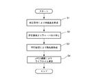
- FIG. 1 is a flow showing the steps of the metal contamination evaluation method according to the present invention.
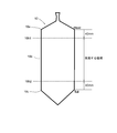
- FIG. 2 is a side view of a single crystal showing a region of a single crystal portion cut out of a silicon wafer used in the metal contamination evaluation method according to the present invention.
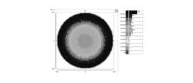
- FIG. 3 is a distribution diagram showing the results of Example 1 of the metal contamination evaluation method according to the present invention.
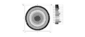
- FIG. 4 is a distribution diagram showing the results of Example 2 of the metal contamination evaluation method according to the present invention.
- FIG. 5 is a distribution diagram showing the results of Example 3 of the metal contamination evaluation method according to the present invention.
- FIG. 6 is a graph showing the results of Example 4 and Comparative Examples 1 and 2 of the metal contamination evaluation method according to the present invention.
- FIG. 7 is a graph showing the results of Example 5 and Comparative Example 3 of the metal contamination evaluation method according to the present invention.
- FIG. 8 is a graph showing the results of Example 6 of the metal contamination evaluation method according to the present invention.
- FIG. 9 is a graph showing the results of Examples 7 to 11 of the metal contamination evaluation method according to the present invention.
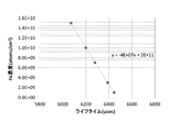
- FIG. 10 is a graph showing the correlation between the lifetime value obtained by the arithmetic expression and the Fe concentration.
- the metal contamination evaluation method of the present invention is a method for evaluating metal contamination in a high-speed heat treatment apparatus (hereinafter also referred to as an RTP apparatus). Specifically, an RTO (rapid thermal oxidation) film is formed on a wafer by cutting a silicon wafer from a silicon single crystal pulled up under a predetermined growth condition, and heat treating it in an oxidizing atmosphere at a predetermined temperature in an RTP apparatus. Do. Then, the contaminants from the members constituting the RTP apparatus are thermally transferred to the wafer, and the wafer is subjected to passivation processing using corona charge. The metal contamination in the furnace is detected by measuring the lifetime of the wafer thus obtained.
- RTP apparatus high-speed heat treatment apparatus
- a silicon single crystal for growing a silicon wafer for metal contamination evaluation is grown (Step S1 in FIG. 1). That is, according to the Czochralski method, the single crystal has an oxygen concentration of 1.3 ⁇ 10 18 atoms / cm 3 (old ASTM) or less, a dopant concentration of 5 ⁇ 10 14 atoms / cm 3 or less, and a pulling rate of 1 mm / min or less It is pulled up on condition of.
- the dopant concentration is 5 ⁇ 10 14 atoms / cm 3 or less, that is, if the substrate resistance is high, the effect of recombination of majority carriers on the wafer surface tends to appear in lifetime evaluation, so the true value of the lifetime is Is difficult to obtain.
- metal contamination can be accurately evaluated even if the dopant concentration is 5 ⁇ 10 14 atoms / cm 3 or less because the influence of surface recombination is small. .
- the straight body portion 10b receiving a long heat history at low temperature from the head shoulder 10a side to the center side 40 mm position 10b1, and the tail cone 10c side A silicon wafer is cut out from the area (area to be used) except for the position 10b2 of 40 mm on the central side from the center of the silicon wafer (step S2 in FIG. 1).
- the reason why the outside of this region can not be applied is that the heat in the crystal is dissipated from the top and bottom of the ingot outside this region (the crystal tends to cool) and the formation of vacancy type defects while the V concentration (Bacansee (vacancy) concentration) remains high. Since the temperature range is reached, the concentration of the vacancy defects increases as a result, and the lifetime decreases.
- the limitation of the oxygen concentration, the pulling rate, etc. as described above is due to the formation effect of the vacancy type defect which causes the lifetime to decrease.
- the substance of the vacancy-type defect has not been clarified, the form is considered to be a complex of VO, VO 2 (V: Bacansee (pore), O: oxygen).
- the formation temperature zone of such a vacancy type defect is considered to be around 1000 ° C. to 800 ° C. in the cooling process of the crystal.
- V (voids) and I (interstitial Si) taken into the crystal at a thermal equilibrium concentration at the solid-liquid interface of the Czochralski crystal are annihilated in the process of cooling the crystal, and the concentration decreases.
- the oxygen concentration is preferably 1.3 ⁇ 10 18 atoms / cm 3 (old ASTM) or less in order to promote formation of vacancy-type defects when the oxygen concentration is high.
- the silicon wafer is held by an RTP apparatus in an oxidizing atmosphere at a temperature of 1100 ° C. or more and a silicon melting point or less for 1 to 60 seconds. Thereafter, the temperature is lowered at 5 to 150 ° C./sec to form an oxide film (RTO film) having a film thickness of 2 nm or more on the silicon wafer (Step S3 in FIG. 1).
- RTO film oxide film
- the use at higher temperatures promotes the outward diffusion of metal impurities present in the members constituting the device.
- the metal impurities in the furnace can be sufficiently transferred to the wafer.
- oxygen and vacancies in the wafer are electrically activated by the RTP process, which causes a decrease in lifetime.
- the silicon wafer obtained under the condition of step S1 it is possible to suppress the decrease of the lifetime due to the vacancy type because there is almost no oxygen or the vacancy, and to measure only the lifetime decrease according to the metal impurities. it can.
- the lifetime is measured by the ⁇ PCD method using the silicon wafer as passivation of corona charge (step S4 in FIG. 1).
- charge is generated and controlled in the atmosphere.
- the charge state of the silicon wafer surface can be controlled and made uniform.
- the lifetime is measured at a laser wavelength of 904 nm, a carrier injection amount of 5 ⁇ 10 13 / cm 3 and a 4 mm pitch.
- excess carriers are generated by applying a pulse to a silicon wafer with a laser beam, which disappears by recombination and returns to the original equilibrium state.
- the change in the excess carrier density at this time is an exponential change in the resistivity of the light irradiation area, and the power of the reflected microwave also changes accordingly.
- the difference in reflected microwave power before and after the light pulse irradiation corresponds to the difference in resistivity, ie, the difference in carrier density, and the lifetime is determined from the time change.
- An RTO film is formed by performing RTP processing in an oxidizing atmosphere at a high temperature of 1100 ° C. or more and a melting point or less using the cut-out wafer to thermally transfer the contaminants from the RTP device member to the wafer, and this wafer is corona-treated.
- the charge passivation process is performed to measure the lifetime by the ⁇ PCD method.
- the method for evaluating metal contamination according to the present invention is not limited to this, and it is also possible to use silicon wafers to which other passivation techniques are applied. It can apply.
- the ⁇ PCD apparatus is used for measuring the lifetime, the present invention is not limited to this, and the lifetime may be measured by another method.
- the metal contamination evaluation method according to the present invention will be further described based on examples.
- the following experiment was performed based on the above embodiment.
- Example 1 In Experiment 1, using the wafers under different growth conditions, the lifetime measurement described in the present embodiment was performed.
- Example 2 P type grown under conditions of oxygen concentration 0.8 ⁇ 10 18 atoms / cm 3 , dopant (boron) concentration 3.7 ⁇ 10 14 atoms / cm 3 and pulling speed 1.5 mm / min. A resistance 36 ⁇ ⁇ cm wafer was used.
- Example 3 N type grown under conditions of oxygen concentration 0.9 ⁇ 10 18 atoms / cm 3 , dopant (phosphorus) concentration 3.0 ⁇ 10 13 atoms / cm 3 , and pulling speed 1.5 mm / min. A wafer with a resistance of 142 ⁇ ⁇ cm was used.
- FIGS. 3, 4 and 5 are distribution maps in which the lifetime values in the wafer plane are classified by color.
- the lifetime average value was 1280 ⁇ sec, and as shown in FIG. 3, local contamination and contamination of the outer periphery were recognized. This was considered to be contamination from the outer periphery of the back surface of the wafer held by the SiC ring during RTP processing. That is, when the wafer of the conditions of Example 1 was used, it has confirmed that metal contamination distribution could be grasped
- the lifetime average values were both 1080 ⁇ sec, and as shown in FIGS. 4 and 5, respectively, the lifetime reduction due to the vacancy type defect was recognized.
- the lifetime reduction caused by the vacancy defects has an effect on the entire surface of the wafer, but the effect is greater at the central portion. This is considered to be caused by the pull-up speed of 1.5 mm / min in each of Examples 2 and 3, which is too fast.
- Example 2 In Experiment 2, the lifetime measurement values for the resistivity, and the surface recombination velocity for Example 4 (RTO film + corona charge), Comparative example 1 (thermal oxide film) and Comparative example 2 (HF passivation) different in passivation method. It verified about the relation with.
- the graph of FIG. 6 shows the results of Example 4 and Comparative Examples 1 and 2.
- the vertical axis is the lifetime value
- the horizontal axis is the resistance value of the P-type wafer.
- curves of surface recombination velocity S 5 cm / s, 10 cm / s, 20 cm / s, and 40 cm / s are shown in the figure.
- S 20 cm / s for thermal oxidation
- S 20 to 40 cm / s for HF passivation.
- Example 3 In Experiment 3, the correlation between the lifetime value and the Fe-B concentration was verified.
- a p-type wafer (oxygen concentration 0.8 ⁇ 10 18 atoms / cm 3 , dopant concentration 7.8 ⁇ 10 14 atoms / cm 3 , pulling rate 0.6 mm / min) was used.
- RTO film formation and corona charge passivation were performed according to the form, lifetime was measured, and the Fe-B concentration was determined by the SPV method.
- Comparative Example 3 a p-type wafer cut out under the same conditions was subjected to HF passivation, lifetime measurement was performed, and the Fe-B concentration was determined by the SPV method.
- Example 5 and Comparative Example 3 are shown in the graph of FIG. In the graph of FIG. 7, the vertical axis is the lifetime value, and the horizontal axis is the Fe-B concentration. As shown in the graph of FIG. 7, in Example 5, a strong correlation was observed between the lifetime value and the Fe-B concentration. On the other hand, in Comparative Example 3, a long correlation was not obtained because a long lifetime value could not be obtained.
- Example 4 In Experiment 4, the condition of the wafer used was different from Experiment 3 to verify the correlation between the lifetime value and the Fe-B concentration.
- Example 6 a p-type wafer (oxygen concentration 0.8 ⁇ 10 18 atoms / cm 3 , dopant (boron) concentration 3.7 ⁇ 10 14 atoms / cm 3 , pulling rate 1.5 mm / min) is used. According to this embodiment, RTO film formation and corona charge passivation were performed to measure the lifetime, and the Fe-B concentration was determined by the SPV method.
- Example 6 The results of Example 6 are shown in the graph of FIG. In the graph of FIG. 8, the vertical axis is the lifetime value, and the horizontal axis is the Fe-B concentration. As shown in the graph of FIG. 8, in Example 6, no correlation was found between the lifetime value and the Fe-B concentration. In addition, the lifetime was reduced due to oxygen and holes, which was considered to be because the single crystal pulling up speed was too fast, 1.5 mm / min.
- Equation (1) when the calculated lifetime value is ⁇ , ⁇ b is the bulk lifetime and ⁇ s is the surface recombination lifetime.
- equation (2) for obtaining the bulk lifetime ⁇ b uses the equation of Shockley lead hole.
- n 0 and p 0 are carrier concentrations of electrons and holes at equilibrium
- ⁇ n and ⁇ p are injected carrier concentrations
- th th is the thermal velocity of carriers
- n i is the intrinsic carrier concentration
- Ei is the intrinsic energy standard
- ⁇ n and ⁇ p are capture cross sections for impurities electrons and holes
- N t is impurity carrier concentration
- E t impurity energy level
- k Boltzmann's constant
- T temperature.
- the impurity was assumed to be Fe, the level (E t ) was 0.4 eV, and the capture cross section ⁇ n was assumed to be 3.6 ⁇ 10 -15 cm 2 .
- the dopant (phosphorus) concentration n 0 of the wafer is 1 ⁇ 10 14 atoms / cm 3 and the temperature (T) is 300K.
- the injection carriers ⁇ n and ⁇ p are determined by using a laser of 904 nm and injecting 5 ⁇ 10 13 / cm 2 when lifetime measurement is performed by the ⁇ PCD apparatus in the standard mode. It becomes a value divided by 775 ⁇ m).
- S is the surface recombination velocity.
- tau dif the diffusion term in the front and back surfaces of the surface recombination lifetime
- tau sr recombination term in the front and back surfaces
- the Fe contamination concentration can be obtained with high accuracy by obtaining the measured value of the lifetime by the metal contamination evaluation method according to the present invention.
- Example 6 the growth conditions of the single crystal cut out from the silicon wafer used in the metal contamination evaluation method according to the present invention were further verified. Specifically, it verified about the range of a suitable pulling up rate and the range of oxygen concentration. In this experiment, conditions of single crystal pulling rate and oxygen concentration were set as shown in Table 1, and RTO film formation and corona charge passivation were performed for Examples 12 to 26, and lifetime measurement was performed using a ⁇ PCD apparatus. .
- the P type 36 ⁇ ⁇ cm, the dopant concentration boron 3.7 ⁇ 10 14 / cm 3 , the crystal part from which the wafer is cut out is the central part of the crystal with a total length of 1000 mm or more, and the conditions of the RTP apparatus are oxygen atmosphere.
- the temperature was lowered to 120 ° C./s at 1350 ° C. ⁇ 30 sec, to 600 ° C.
- the lifetime average value (lifetime in-plane average value) in the wafer surface obtained from the example under each condition is 3800 ⁇ sec, where the theoretical lifetime value (called ⁇ SRH ) estimated from the dopant concentration is 3800 ⁇ sec, It was considered as a rejection (decision x in Table 1) when it was less than 50% (1900 ⁇ sec) of ⁇ SRH , and was passed (decision ⁇ in Table 1) when it was 50% or more.
- Example 7 In Experiment 7, the conditions of the cutout position were set in Examples 27 to 35 in order to specify the position where the wafer was cut out from the single crystal, and evaluation was performed on the in-plane average value in the same manner as Experiment 6. Table 2 shows the conditions and experimental results of Examples 27 to 35.
- the pulling rate is 0.6 mm / min
- the oxygen concentration is 1.2 ⁇ 10 18 / cm 3
- the other conditions are the same as in Experiment 6.
- the pulling rate of silicon single crystal is 1.0 mm / min or less
- oxygen concentration is 1.3 ⁇ 10 18 / cm 3 or less
- the crystal site from which the wafer is cut is 40 mm from the head and 40 mm from the tail
- the reduction of the lifetime due to the vacancy type can be suppressed, and the metal contamination amount can be accurately evaluated by the lifetime measurement due to the metal contamination.
Landscapes
- Engineering & Computer Science (AREA)
- Manufacturing & Machinery (AREA)
- Chemical & Material Sciences (AREA)
- Power Engineering (AREA)
- Microelectronics & Electronic Packaging (AREA)
- Computer Hardware Design (AREA)
- Physics & Mathematics (AREA)
- General Physics & Mathematics (AREA)
- Health & Medical Sciences (AREA)
- Organic Chemistry (AREA)
- Crystallography & Structural Chemistry (AREA)
- Materials Engineering (AREA)
- Metallurgy (AREA)
- Condensed Matter Physics & Semiconductors (AREA)
- Analytical Chemistry (AREA)
- Nuclear Medicine, Radiotherapy & Molecular Imaging (AREA)
- Pathology (AREA)
- Immunology (AREA)
- Life Sciences & Earth Sciences (AREA)
- General Health & Medical Sciences (AREA)
- Biochemistry (AREA)
- Plasma & Fusion (AREA)
- High Energy & Nuclear Physics (AREA)
- Toxicology (AREA)
- Testing Or Measuring Of Semiconductors Or The Like (AREA)
- Crystals, And After-Treatments Of Crystals (AREA)
Priority Applications (4)
| Application Number | Priority Date | Filing Date | Title |
|---|---|---|---|
| KR1020207021032A KR102463966B1 (ko) | 2017-12-22 | 2018-08-02 | 금속 오염 평가 방법 |
| EP18891783.5A EP3731263A4 (en) | 2017-12-22 | 2018-08-02 | METAL CONTAMINATION ASSESSMENT PROCESS |
| CN201880082997.6A CN111480219A (zh) | 2017-12-22 | 2018-08-02 | 金属污染评价方法 |
| US16/956,282 US11538721B2 (en) | 2017-12-22 | 2018-08-02 | Evaluation method of metal contamination |
Applications Claiming Priority (2)
| Application Number | Priority Date | Filing Date | Title |
|---|---|---|---|
| JP2017246190A JP7057122B2 (ja) | 2017-12-22 | 2017-12-22 | 金属汚染評価方法 |
| JP2017-246190 | 2017-12-22 |
Publications (1)
| Publication Number | Publication Date |
|---|---|
| WO2019123706A1 true WO2019123706A1 (ja) | 2019-06-27 |
Family
ID=66994648
Family Applications (1)
| Application Number | Title | Priority Date | Filing Date |
|---|---|---|---|
| PCT/JP2018/029009 WO2019123706A1 (ja) | 2017-12-22 | 2018-08-02 | 金属汚染評価方法 |
Country Status (7)
| Country | Link |
|---|---|
| US (1) | US11538721B2 (ko) |
| EP (1) | EP3731263A4 (ko) |
| JP (1) | JP7057122B2 (ko) |
| KR (1) | KR102463966B1 (ko) |
| CN (1) | CN111480219A (ko) |
| TW (1) | TWI717628B (ko) |
| WO (1) | WO2019123706A1 (ko) |
Cited By (1)
| Publication number | Priority date | Publication date | Assignee | Title |
|---|---|---|---|---|
| WO2021162046A1 (ja) * | 2020-02-14 | 2021-08-19 | グローバルウェーハズ・ジャパン株式会社 | シリコン単結晶の製造方法 |
Families Citing this family (1)
| Publication number | Priority date | Publication date | Assignee | Title |
|---|---|---|---|---|
| CN112908876A (zh) * | 2021-01-18 | 2021-06-04 | 上海新昇半导体科技有限公司 | 硅片金属污染测试方法及装置 |
Citations (8)
| Publication number | Priority date | Publication date | Assignee | Title |
|---|---|---|---|---|
| JP2004189584A (ja) * | 2002-10-18 | 2004-07-08 | Sumitomo Mitsubishi Silicon Corp | シリコン単結晶インゴットの点欠陥分布を測定する方法 |
| JP2009302337A (ja) | 2008-06-13 | 2009-12-24 | Shin Etsu Handotai Co Ltd | 汚染検出用モニターウェーハ、汚染検出方法及びエピタキシャルウェーハの製造方法 |
| JP2010177494A (ja) * | 2009-01-30 | 2010-08-12 | Covalent Materials Corp | シリコンウェーハの熱処理方法 |
| WO2010119614A1 (ja) * | 2009-04-13 | 2010-10-21 | 信越半導体株式会社 | アニールウエーハおよびアニールウエーハの製造方法ならびにデバイスの製造方法 |
| JP2013084840A (ja) | 2011-10-12 | 2013-05-09 | Shin Etsu Handotai Co Ltd | 金属汚染評価方法及びエピタキシャルウェーハの製造方法 |
| JP2013105914A (ja) * | 2011-11-14 | 2013-05-30 | Shin Etsu Handotai Co Ltd | 気相成長装置の清浄度評価方法 |
| JP2014058414A (ja) * | 2012-09-14 | 2014-04-03 | Jnc Corp | 評価用シリコン単結晶の製造方法 |
| JP2017103275A (ja) * | 2015-11-30 | 2017-06-08 | 株式会社Sumco | シリコンウェーハの評価方法およびその利用 |
Family Cites Families (15)
| Publication number | Priority date | Publication date | Assignee | Title |
|---|---|---|---|---|
| GB0216184D0 (en) * | 2002-07-12 | 2002-08-21 | Aoti Operating Co Inc | Detection method and apparatus |
| DE60335409D1 (de) | 2002-10-18 | 2011-01-27 | Sumco Corp | Verfahren zur bestimmung derpunktdefektverteilung eines siliciumeinkristallstabs |
| KR100500712B1 (ko) * | 2002-12-16 | 2005-07-11 | 주식회사 실트론 | 실리콘웨이퍼의 금속 불순물 농도 측정 방법 |
| JP2009266835A (ja) * | 2008-04-21 | 2009-11-12 | Sumco Corp | シリコン単結晶の金属汚染評価方法 |
| US8252700B2 (en) | 2009-01-30 | 2012-08-28 | Covalent Materials Corporation | Method of heat treating silicon wafer |
| JP5467923B2 (ja) * | 2010-05-06 | 2014-04-09 | 信越半導体株式会社 | 金属汚染評価用シリコンウエーハの製造方法 |
| JP5621612B2 (ja) | 2011-01-19 | 2014-11-12 | 株式会社Sumco | シリコン単結晶の検査方法および製造方法 |
| JP5742742B2 (ja) * | 2012-02-08 | 2015-07-01 | 信越半導体株式会社 | 金属汚染評価方法 |
| JP5733245B2 (ja) | 2012-03-16 | 2015-06-10 | 信越半導体株式会社 | シリコン単結晶ウェーハの製造方法 |
| DE102012214085B4 (de) | 2012-08-08 | 2016-07-07 | Siltronic Ag | Halbleiterscheibe aus einkristallinem Silizium und Verfahren zu deren Herstellung |
| JP6266653B2 (ja) | 2013-01-08 | 2018-01-24 | エスケー シルトロン カンパニー リミテッド | シリコン単結晶ウェハ |
| EP2779220B1 (en) * | 2013-03-12 | 2017-10-25 | GLobalWafers Japan Co., Ltd. | Saturation voltage estimation method and silicon epitaxial wafer manufaturing method |
| JP5885305B2 (ja) * | 2013-08-07 | 2016-03-15 | グローバルウェーハズ・ジャパン株式会社 | シリコンウェーハ及びその製造方法 |
| JP6044660B2 (ja) | 2015-02-19 | 2016-12-14 | 信越半導体株式会社 | シリコンウェーハの製造方法 |
| DE102015224983B4 (de) | 2015-12-11 | 2019-01-24 | Siltronic Ag | Halbleiterscheibe aus einkristallinem Silizium und Verfahren zu deren Herstellung |
-
2017
- 2017-12-22 JP JP2017246190A patent/JP7057122B2/ja active Active
-
2018
- 2018-08-02 US US16/956,282 patent/US11538721B2/en active Active
- 2018-08-02 WO PCT/JP2018/029009 patent/WO2019123706A1/ja unknown
- 2018-08-02 EP EP18891783.5A patent/EP3731263A4/en active Pending
- 2018-08-02 CN CN201880082997.6A patent/CN111480219A/zh active Pending
- 2018-08-02 KR KR1020207021032A patent/KR102463966B1/ko active IP Right Grant
- 2018-08-17 TW TW107128807A patent/TWI717628B/zh active
Patent Citations (8)
| Publication number | Priority date | Publication date | Assignee | Title |
|---|---|---|---|---|
| JP2004189584A (ja) * | 2002-10-18 | 2004-07-08 | Sumitomo Mitsubishi Silicon Corp | シリコン単結晶インゴットの点欠陥分布を測定する方法 |
| JP2009302337A (ja) | 2008-06-13 | 2009-12-24 | Shin Etsu Handotai Co Ltd | 汚染検出用モニターウェーハ、汚染検出方法及びエピタキシャルウェーハの製造方法 |
| JP2010177494A (ja) * | 2009-01-30 | 2010-08-12 | Covalent Materials Corp | シリコンウェーハの熱処理方法 |
| WO2010119614A1 (ja) * | 2009-04-13 | 2010-10-21 | 信越半導体株式会社 | アニールウエーハおよびアニールウエーハの製造方法ならびにデバイスの製造方法 |
| JP2013084840A (ja) | 2011-10-12 | 2013-05-09 | Shin Etsu Handotai Co Ltd | 金属汚染評価方法及びエピタキシャルウェーハの製造方法 |
| JP2013105914A (ja) * | 2011-11-14 | 2013-05-30 | Shin Etsu Handotai Co Ltd | 気相成長装置の清浄度評価方法 |
| JP2014058414A (ja) * | 2012-09-14 | 2014-04-03 | Jnc Corp | 評価用シリコン単結晶の製造方法 |
| JP2017103275A (ja) * | 2015-11-30 | 2017-06-08 | 株式会社Sumco | シリコンウェーハの評価方法およびその利用 |
Non-Patent Citations (1)
| Title |
|---|
| See also references of EP3731263A4 |
Cited By (1)
| Publication number | Priority date | Publication date | Assignee | Title |
|---|---|---|---|---|
| WO2021162046A1 (ja) * | 2020-02-14 | 2021-08-19 | グローバルウェーハズ・ジャパン株式会社 | シリコン単結晶の製造方法 |
Also Published As
| Publication number | Publication date |
|---|---|
| TW201929111A (zh) | 2019-07-16 |
| EP3731263A4 (en) | 2021-09-08 |
| JP7057122B2 (ja) | 2022-04-19 |
| US20210082774A1 (en) | 2021-03-18 |
| KR102463966B1 (ko) | 2022-11-04 |
| CN111480219A (zh) | 2020-07-31 |
| JP2019114633A (ja) | 2019-07-11 |
| KR20200100783A (ko) | 2020-08-26 |
| TWI717628B (zh) | 2021-02-01 |
| US11538721B2 (en) | 2022-12-27 |
| EP3731263A1 (en) | 2020-10-28 |
Similar Documents
| Publication | Publication Date | Title |
|---|---|---|
| TWI539041B (zh) | 單晶矽半導體晶圓及其製造方法 | |
| US7759227B2 (en) | Silicon semiconductor substrate heat-treatment method and silicon semiconductor substrate treated by the method | |
| US20050247259A1 (en) | Silicon wafer and method for manufacturing the same | |
| JP2007088421A (ja) | シリコンウェーハの表面欠陥評価方法 | |
| WO2019123706A1 (ja) | 金属汚染評価方法 | |
| KR100722089B1 (ko) | 실리콘 단결정 잉곳의 점결함 분포를 측정하는 방법 | |
| US20100052103A1 (en) | Silicon wafer and method for producing the same | |
| EP2587527B1 (en) | Silicon wafer and its manufacturing method | |
| Zheng et al. | Evidence for vacancy-related Recombination Active Defects in as-grown n-type Czochralski Silicon | |
| US11639558B2 (en) | Method for producing a semiconductor wafer composed of monocrystalline silicon | |
| JP3933010B2 (ja) | シリコン単結晶インゴットの点欠陥分布を測定する方法 | |
| CN105470129B (zh) | 一种消除氧热施主对少子扩散长度影响的方法 | |
| CN105900220B (zh) | 单晶硅晶圆的热处理方法 | |
| US8460463B2 (en) | Silicon wafer and method for producing the same | |
| JP4200845B2 (ja) | シリコン単結晶インゴットの点欠陥分布を測定する方法 | |
| JP2019149416A (ja) | エピタキシャルシリコンウェーハの製造方法及びエピタキシャルシリコンウェーハ | |
| JP2004020341A (ja) | シリコン単結晶インゴットの点欠陥分布を測定する方法 | |
| Tardif | CRYSTALLINE DEPECTS AND CONTAMINATION: T-EIR| MPACT AND CONTROL| N| DEVICE MANUFACTURING | |
| JP3731553B2 (ja) | シリコンウェーハの窒素濃度の評価方法 | |
| JP6459900B2 (ja) | シリコンウェーハの検査方法 | |
| JP2002353282A (ja) | シリコン単結晶ウェーハ中の窒素濃度の評価方法 | |
| Looney et al. | Tabula Rasa: Oxygen precipitate dissolution though rapid high temperature processing in silicon | |
| JPH11283986A (ja) | シリコン基板の熱処理条件を設定する方法、およびシリコン基板を熱処理する方法、並びにシリコン基板の製造方法 |
Legal Events
| Date | Code | Title | Description |
|---|---|---|---|
| 121 | Ep: the epo has been informed by wipo that ep was designated in this application |
Ref document number: 18891783 Country of ref document: EP Kind code of ref document: A1 |
|
| NENP | Non-entry into the national phase |
Ref country code: DE |
|
| ENP | Entry into the national phase |
Ref document number: 20207021032 Country of ref document: KR Kind code of ref document: A |
|
| ENP | Entry into the national phase |
Ref document number: 2018891783 Country of ref document: EP Effective date: 20200722 |