WO2019123706A1 - Metal contamination evaluation method - Google Patents
Metal contamination evaluation method Download PDFInfo
- Publication number
- WO2019123706A1 WO2019123706A1 PCT/JP2018/029009 JP2018029009W WO2019123706A1 WO 2019123706 A1 WO2019123706 A1 WO 2019123706A1 JP 2018029009 W JP2018029009 W JP 2018029009W WO 2019123706 A1 WO2019123706 A1 WO 2019123706A1
- Authority
- WO
- WIPO (PCT)
- Prior art keywords
- lifetime
- silicon wafer
- metal contamination
- silicon
- concentration
- Prior art date
Links
Images

Classifications
-
- H—ELECTRICITY
- H01—ELECTRIC ELEMENTS
- H01L—SEMICONDUCTOR DEVICES NOT COVERED BY CLASS H10
- H01L22/00—Testing or measuring during manufacture or treatment; Reliability measurements, i.e. testing of parts without further processing to modify the parts as such; Structural arrangements therefor
- H01L22/10—Measuring as part of the manufacturing process
- H01L22/12—Measuring as part of the manufacturing process for structural parameters, e.g. thickness, line width, refractive index, temperature, warp, bond strength, defects, optical inspection, electrical measurement of structural dimensions, metallurgic measurement of diffusions
-
- C—CHEMISTRY; METALLURGY
- C30—CRYSTAL GROWTH
- C30B—SINGLE-CRYSTAL GROWTH; UNIDIRECTIONAL SOLIDIFICATION OF EUTECTIC MATERIAL OR UNIDIRECTIONAL DEMIXING OF EUTECTOID MATERIAL; REFINING BY ZONE-MELTING OF MATERIAL; PRODUCTION OF A HOMOGENEOUS POLYCRYSTALLINE MATERIAL WITH DEFINED STRUCTURE; SINGLE CRYSTALS OR HOMOGENEOUS POLYCRYSTALLINE MATERIAL WITH DEFINED STRUCTURE; AFTER-TREATMENT OF SINGLE CRYSTALS OR A HOMOGENEOUS POLYCRYSTALLINE MATERIAL WITH DEFINED STRUCTURE; APPARATUS THEREFOR
- C30B15/00—Single-crystal growth by pulling from a melt, e.g. Czochralski method
- C30B15/14—Heating of the melt or the crystallised materials
-
- C—CHEMISTRY; METALLURGY
- C30—CRYSTAL GROWTH
- C30B—SINGLE-CRYSTAL GROWTH; UNIDIRECTIONAL SOLIDIFICATION OF EUTECTIC MATERIAL OR UNIDIRECTIONAL DEMIXING OF EUTECTOID MATERIAL; REFINING BY ZONE-MELTING OF MATERIAL; PRODUCTION OF A HOMOGENEOUS POLYCRYSTALLINE MATERIAL WITH DEFINED STRUCTURE; SINGLE CRYSTALS OR HOMOGENEOUS POLYCRYSTALLINE MATERIAL WITH DEFINED STRUCTURE; AFTER-TREATMENT OF SINGLE CRYSTALS OR A HOMOGENEOUS POLYCRYSTALLINE MATERIAL WITH DEFINED STRUCTURE; APPARATUS THEREFOR
- C30B15/00—Single-crystal growth by pulling from a melt, e.g. Czochralski method
- C30B15/20—Controlling or regulating
- C30B15/203—Controlling or regulating the relationship of pull rate (v) to axial thermal gradient (G)
-
- C—CHEMISTRY; METALLURGY
- C30—CRYSTAL GROWTH
- C30B—SINGLE-CRYSTAL GROWTH; UNIDIRECTIONAL SOLIDIFICATION OF EUTECTIC MATERIAL OR UNIDIRECTIONAL DEMIXING OF EUTECTOID MATERIAL; REFINING BY ZONE-MELTING OF MATERIAL; PRODUCTION OF A HOMOGENEOUS POLYCRYSTALLINE MATERIAL WITH DEFINED STRUCTURE; SINGLE CRYSTALS OR HOMOGENEOUS POLYCRYSTALLINE MATERIAL WITH DEFINED STRUCTURE; AFTER-TREATMENT OF SINGLE CRYSTALS OR A HOMOGENEOUS POLYCRYSTALLINE MATERIAL WITH DEFINED STRUCTURE; APPARATUS THEREFOR
- C30B29/00—Single crystals or homogeneous polycrystalline material with defined structure characterised by the material or by their shape
- C30B29/02—Elements
- C30B29/06—Silicon
-
- G—PHYSICS
- G01—MEASURING; TESTING
- G01N—INVESTIGATING OR ANALYSING MATERIALS BY DETERMINING THEIR CHEMICAL OR PHYSICAL PROPERTIES
- G01N21/00—Investigating or analysing materials by the use of optical means, i.e. using sub-millimetre waves, infrared, visible or ultraviolet light
- G01N21/62—Systems in which the material investigated is excited whereby it emits light or causes a change in wavelength of the incident light
- G01N21/63—Systems in which the material investigated is excited whereby it emits light or causes a change in wavelength of the incident light optically excited
- G01N21/64—Fluorescence; Phosphorescence
- G01N21/6408—Fluorescence; Phosphorescence with measurement of decay time, time resolved fluorescence
-
- G—PHYSICS
- G01—MEASURING; TESTING
- G01N—INVESTIGATING OR ANALYSING MATERIALS BY DETERMINING THEIR CHEMICAL OR PHYSICAL PROPERTIES
- G01N21/00—Investigating or analysing materials by the use of optical means, i.e. using sub-millimetre waves, infrared, visible or ultraviolet light
- G01N21/62—Systems in which the material investigated is excited whereby it emits light or causes a change in wavelength of the incident light
- G01N21/63—Systems in which the material investigated is excited whereby it emits light or causes a change in wavelength of the incident light optically excited
- G01N21/64—Fluorescence; Phosphorescence
- G01N21/6489—Photoluminescence of semiconductors
-
- H—ELECTRICITY
- H01—ELECTRIC ELEMENTS
- H01J—ELECTRIC DISCHARGE TUBES OR DISCHARGE LAMPS
- H01J37/00—Discharge tubes with provision for introducing objects or material to be exposed to the discharge, e.g. for the purpose of examination or processing thereof
- H01J37/32—Gas-filled discharge tubes
- H01J37/32009—Arrangements for generation of plasma specially adapted for examination or treatment of objects, e.g. plasma sources
- H01J37/32073—Corona discharge
-
- H—ELECTRICITY
- H01—ELECTRIC ELEMENTS
- H01L—SEMICONDUCTOR DEVICES NOT COVERED BY CLASS H10
- H01L21/00—Processes or apparatus adapted for the manufacture or treatment of semiconductor or solid state devices or of parts thereof
- H01L21/02—Manufacture or treatment of semiconductor devices or of parts thereof
- H01L21/02104—Forming layers
-
- H—ELECTRICITY
- H01—ELECTRIC ELEMENTS
- H01L—SEMICONDUCTOR DEVICES NOT COVERED BY CLASS H10
- H01L21/00—Processes or apparatus adapted for the manufacture or treatment of semiconductor or solid state devices or of parts thereof
- H01L21/02—Manufacture or treatment of semiconductor devices or of parts thereof
- H01L21/04—Manufacture or treatment of semiconductor devices or of parts thereof the devices having at least one potential-jump barrier or surface barrier, e.g. PN junction, depletion layer or carrier concentration layer
- H01L21/18—Manufacture or treatment of semiconductor devices or of parts thereof the devices having at least one potential-jump barrier or surface barrier, e.g. PN junction, depletion layer or carrier concentration layer the devices having semiconductor bodies comprising elements of Group IV of the Periodic System or AIIIBV compounds with or without impurities, e.g. doping materials
- H01L21/26—Bombardment with radiation
-
- H—ELECTRICITY
- H01—ELECTRIC ELEMENTS
- H01L—SEMICONDUCTOR DEVICES NOT COVERED BY CLASS H10
- H01L21/00—Processes or apparatus adapted for the manufacture or treatment of semiconductor or solid state devices or of parts thereof
- H01L21/02—Manufacture or treatment of semiconductor devices or of parts thereof
- H01L21/04—Manufacture or treatment of semiconductor devices or of parts thereof the devices having at least one potential-jump barrier or surface barrier, e.g. PN junction, depletion layer or carrier concentration layer
- H01L21/18—Manufacture or treatment of semiconductor devices or of parts thereof the devices having at least one potential-jump barrier or surface barrier, e.g. PN junction, depletion layer or carrier concentration layer the devices having semiconductor bodies comprising elements of Group IV of the Periodic System or AIIIBV compounds with or without impurities, e.g. doping materials
- H01L21/30—Treatment of semiconductor bodies using processes or apparatus not provided for in groups H01L21/20 - H01L21/26
- H01L21/322—Treatment of semiconductor bodies using processes or apparatus not provided for in groups H01L21/20 - H01L21/26 to modify their internal properties, e.g. to produce internal imperfections
-
- H—ELECTRICITY
- H01—ELECTRIC ELEMENTS
- H01L—SEMICONDUCTOR DEVICES NOT COVERED BY CLASS H10
- H01L22/00—Testing or measuring during manufacture or treatment; Reliability measurements, i.e. testing of parts without further processing to modify the parts as such; Structural arrangements therefor
- H01L22/20—Sequence of activities consisting of a plurality of measurements, corrections, marking or sorting steps
- H01L22/22—Connection or disconnection of sub-entities or redundant parts of a device in response to a measurement
-
- H—ELECTRICITY
- H01—ELECTRIC ELEMENTS
- H01J—ELECTRIC DISCHARGE TUBES OR DISCHARGE LAMPS
- H01J2237/00—Discharge tubes exposing object to beam, e.g. for analysis treatment, etching, imaging
- H01J2237/245—Detection characterised by the variable being measured
- H01J2237/24592—Inspection and quality control of devices
-
- H—ELECTRICITY
- H01—ELECTRIC ELEMENTS
- H01L—SEMICONDUCTOR DEVICES NOT COVERED BY CLASS H10
- H01L22/00—Testing or measuring during manufacture or treatment; Reliability measurements, i.e. testing of parts without further processing to modify the parts as such; Structural arrangements therefor
- H01L22/20—Sequence of activities consisting of a plurality of measurements, corrections, marking or sorting steps
Definitions
- the present invention relates to a method for evaluating metal contamination, and more particularly, to a method for evaluating metal contamination that can accurately evaluate metal contamination in a furnace in a rapid thermal processing apparatus (RTP apparatus) that heats a silicon wafer at high speed.
- RTP apparatus rapid thermal processing apparatus
- Patent Document 1 Japanese Patent Application Laid-Open No. 2013-84840
- Patent Document 2 Japanese Patent Application Laid-Open No. 2009-302337 disclose metal contamination by treating a high resistance silicon wafer in a heat treatment furnace. It is disclosed that metal impurities are detected by transferring to the silicon wafer and then detecting the Fe-B concentration by the SPV method (surface photovoltaic method) and measuring the lifetime by the ⁇ PCD method (microwave photoconductivity decay method). .
- SPV method surface photovoltaic method
- ⁇ PCD method microwave photoconductivity decay method
- thermal oxidation and HF (hydrofluoric acid) passivation methods are mainly known.
- thermal oxidation a silicon oxide film (thermal oxide film) is formed on a silicon surface by heating, and a good Si—SiO 2 interface is introduced to obtain a surface passivation effect.
- the HF passivation method is chemical passivation using an aqueous solution of HF (hydrofluoric acid).
- the present invention has been made under the circumstances as described above, and it is an object of the present invention to provide a metal contamination evaluation method capable of measuring and evaluating the amount of metal contamination on a silicon wafer in a high speed heat treatment apparatus with high accuracy. I assume.
- the metal contamination evaluation method according to the present invention which was made to solve the above problems, is a metal contamination evaluation method for measuring the amount of metal contamination on a silicon wafer in a high-speed heat treatment apparatus, and is 1.0 mm by the Czochralski method.
- Step of growing silicon single crystal having an oxygen concentration of 1.3 ⁇ 10 18 / cm 3 or less by growing at a pulling rate of less than 1 / min, and 40 mm from the head of the silicon single crystal and 40 mm from the tail to the center Cutting out the silicon wafer from the region excluding the heat treatment, heat-treating the silicon wafer with a high-speed heat treatment apparatus, and thermally transferring the contaminants from the furnace inner member onto the silicon wafer, and with respect to the silicon wafer to which the contaminants are transferred. And measuring the lifetime.
- the step of heat-treating the silicon wafer with a high-speed heat treatment apparatus and thermally transferring the contaminants from the internal members to the silicon wafer after holding for 1 to 60 seconds at a temperature of 1100 ° C. or more and silicon melting point or less under oxidizing gas.
- the temperature is lowered at a rate of 5 to 150 ° C./sec to form an oxide film having a thickness of 2 nm or more on the silicon wafer.
- it is preferable to measure the lifetime after corona charge is used as passivation for the silicon wafer.
- the dopant concentration is 5 ⁇ 10 14. It is desirable to set atoms / cm 3 or less.
- the present invention it is possible to provide a metal contamination evaluation method capable of measuring and evaluating the amount of metal contamination on a silicon wafer in a high-speed heat treatment apparatus with high accuracy.
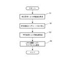
- FIG. 1 is a flow showing the steps of the metal contamination evaluation method according to the present invention.
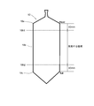
- FIG. 2 is a side view of a single crystal showing a region of a single crystal portion cut out of a silicon wafer used in the metal contamination evaluation method according to the present invention.
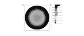
- FIG. 3 is a distribution diagram showing the results of Example 1 of the metal contamination evaluation method according to the present invention.
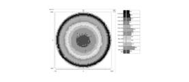
- FIG. 4 is a distribution diagram showing the results of Example 2 of the metal contamination evaluation method according to the present invention.
- FIG. 5 is a distribution diagram showing the results of Example 3 of the metal contamination evaluation method according to the present invention.
- FIG. 6 is a graph showing the results of Example 4 and Comparative Examples 1 and 2 of the metal contamination evaluation method according to the present invention.
- FIG. 7 is a graph showing the results of Example 5 and Comparative Example 3 of the metal contamination evaluation method according to the present invention.
- FIG. 8 is a graph showing the results of Example 6 of the metal contamination evaluation method according to the present invention.
- FIG. 9 is a graph showing the results of Examples 7 to 11 of the metal contamination evaluation method according to the present invention.
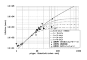
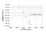
- FIG. 10 is a graph showing the correlation between the lifetime value obtained by the arithmetic expression and the Fe concentration.
- the metal contamination evaluation method of the present invention is a method for evaluating metal contamination in a high-speed heat treatment apparatus (hereinafter also referred to as an RTP apparatus). Specifically, an RTO (rapid thermal oxidation) film is formed on a wafer by cutting a silicon wafer from a silicon single crystal pulled up under a predetermined growth condition, and heat treating it in an oxidizing atmosphere at a predetermined temperature in an RTP apparatus. Do. Then, the contaminants from the members constituting the RTP apparatus are thermally transferred to the wafer, and the wafer is subjected to passivation processing using corona charge. The metal contamination in the furnace is detected by measuring the lifetime of the wafer thus obtained.
- RTP apparatus high-speed heat treatment apparatus
- a silicon single crystal for growing a silicon wafer for metal contamination evaluation is grown (Step S1 in FIG. 1). That is, according to the Czochralski method, the single crystal has an oxygen concentration of 1.3 ⁇ 10 18 atoms / cm 3 (old ASTM) or less, a dopant concentration of 5 ⁇ 10 14 atoms / cm 3 or less, and a pulling rate of 1 mm / min or less It is pulled up on condition of.
- the dopant concentration is 5 ⁇ 10 14 atoms / cm 3 or less, that is, if the substrate resistance is high, the effect of recombination of majority carriers on the wafer surface tends to appear in lifetime evaluation, so the true value of the lifetime is Is difficult to obtain.
- metal contamination can be accurately evaluated even if the dopant concentration is 5 ⁇ 10 14 atoms / cm 3 or less because the influence of surface recombination is small. .
- the straight body portion 10b receiving a long heat history at low temperature from the head shoulder 10a side to the center side 40 mm position 10b1, and the tail cone 10c side A silicon wafer is cut out from the area (area to be used) except for the position 10b2 of 40 mm on the central side from the center of the silicon wafer (step S2 in FIG. 1).
- the reason why the outside of this region can not be applied is that the heat in the crystal is dissipated from the top and bottom of the ingot outside this region (the crystal tends to cool) and the formation of vacancy type defects while the V concentration (Bacansee (vacancy) concentration) remains high. Since the temperature range is reached, the concentration of the vacancy defects increases as a result, and the lifetime decreases.
- the limitation of the oxygen concentration, the pulling rate, etc. as described above is due to the formation effect of the vacancy type defect which causes the lifetime to decrease.
- the substance of the vacancy-type defect has not been clarified, the form is considered to be a complex of VO, VO 2 (V: Bacansee (pore), O: oxygen).
- the formation temperature zone of such a vacancy type defect is considered to be around 1000 ° C. to 800 ° C. in the cooling process of the crystal.
- V (voids) and I (interstitial Si) taken into the crystal at a thermal equilibrium concentration at the solid-liquid interface of the Czochralski crystal are annihilated in the process of cooling the crystal, and the concentration decreases.
- the oxygen concentration is preferably 1.3 ⁇ 10 18 atoms / cm 3 (old ASTM) or less in order to promote formation of vacancy-type defects when the oxygen concentration is high.
- the silicon wafer is held by an RTP apparatus in an oxidizing atmosphere at a temperature of 1100 ° C. or more and a silicon melting point or less for 1 to 60 seconds. Thereafter, the temperature is lowered at 5 to 150 ° C./sec to form an oxide film (RTO film) having a film thickness of 2 nm or more on the silicon wafer (Step S3 in FIG. 1).
- RTO film oxide film
- the use at higher temperatures promotes the outward diffusion of metal impurities present in the members constituting the device.
- the metal impurities in the furnace can be sufficiently transferred to the wafer.
- oxygen and vacancies in the wafer are electrically activated by the RTP process, which causes a decrease in lifetime.
- the silicon wafer obtained under the condition of step S1 it is possible to suppress the decrease of the lifetime due to the vacancy type because there is almost no oxygen or the vacancy, and to measure only the lifetime decrease according to the metal impurities. it can.
- the lifetime is measured by the ⁇ PCD method using the silicon wafer as passivation of corona charge (step S4 in FIG. 1).
- charge is generated and controlled in the atmosphere.
- the charge state of the silicon wafer surface can be controlled and made uniform.
- the lifetime is measured at a laser wavelength of 904 nm, a carrier injection amount of 5 ⁇ 10 13 / cm 3 and a 4 mm pitch.
- excess carriers are generated by applying a pulse to a silicon wafer with a laser beam, which disappears by recombination and returns to the original equilibrium state.
- the change in the excess carrier density at this time is an exponential change in the resistivity of the light irradiation area, and the power of the reflected microwave also changes accordingly.
- the difference in reflected microwave power before and after the light pulse irradiation corresponds to the difference in resistivity, ie, the difference in carrier density, and the lifetime is determined from the time change.
- An RTO film is formed by performing RTP processing in an oxidizing atmosphere at a high temperature of 1100 ° C. or more and a melting point or less using the cut-out wafer to thermally transfer the contaminants from the RTP device member to the wafer, and this wafer is corona-treated.
- the charge passivation process is performed to measure the lifetime by the ⁇ PCD method.
- the method for evaluating metal contamination according to the present invention is not limited to this, and it is also possible to use silicon wafers to which other passivation techniques are applied. It can apply.
- the ⁇ PCD apparatus is used for measuring the lifetime, the present invention is not limited to this, and the lifetime may be measured by another method.
- the metal contamination evaluation method according to the present invention will be further described based on examples.
- the following experiment was performed based on the above embodiment.
- Example 1 In Experiment 1, using the wafers under different growth conditions, the lifetime measurement described in the present embodiment was performed.
- Example 2 P type grown under conditions of oxygen concentration 0.8 ⁇ 10 18 atoms / cm 3 , dopant (boron) concentration 3.7 ⁇ 10 14 atoms / cm 3 and pulling speed 1.5 mm / min. A resistance 36 ⁇ ⁇ cm wafer was used.
- Example 3 N type grown under conditions of oxygen concentration 0.9 ⁇ 10 18 atoms / cm 3 , dopant (phosphorus) concentration 3.0 ⁇ 10 13 atoms / cm 3 , and pulling speed 1.5 mm / min. A wafer with a resistance of 142 ⁇ ⁇ cm was used.
- FIGS. 3, 4 and 5 are distribution maps in which the lifetime values in the wafer plane are classified by color.
- the lifetime average value was 1280 ⁇ sec, and as shown in FIG. 3, local contamination and contamination of the outer periphery were recognized. This was considered to be contamination from the outer periphery of the back surface of the wafer held by the SiC ring during RTP processing. That is, when the wafer of the conditions of Example 1 was used, it has confirmed that metal contamination distribution could be grasped
- the lifetime average values were both 1080 ⁇ sec, and as shown in FIGS. 4 and 5, respectively, the lifetime reduction due to the vacancy type defect was recognized.
- the lifetime reduction caused by the vacancy defects has an effect on the entire surface of the wafer, but the effect is greater at the central portion. This is considered to be caused by the pull-up speed of 1.5 mm / min in each of Examples 2 and 3, which is too fast.
- Example 2 In Experiment 2, the lifetime measurement values for the resistivity, and the surface recombination velocity for Example 4 (RTO film + corona charge), Comparative example 1 (thermal oxide film) and Comparative example 2 (HF passivation) different in passivation method. It verified about the relation with.
- the graph of FIG. 6 shows the results of Example 4 and Comparative Examples 1 and 2.
- the vertical axis is the lifetime value
- the horizontal axis is the resistance value of the P-type wafer.
- curves of surface recombination velocity S 5 cm / s, 10 cm / s, 20 cm / s, and 40 cm / s are shown in the figure.
- S 20 cm / s for thermal oxidation
- S 20 to 40 cm / s for HF passivation.
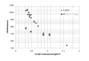
- Example 3 In Experiment 3, the correlation between the lifetime value and the Fe-B concentration was verified.
- a p-type wafer (oxygen concentration 0.8 ⁇ 10 18 atoms / cm 3 , dopant concentration 7.8 ⁇ 10 14 atoms / cm 3 , pulling rate 0.6 mm / min) was used.
- RTO film formation and corona charge passivation were performed according to the form, lifetime was measured, and the Fe-B concentration was determined by the SPV method.
- Comparative Example 3 a p-type wafer cut out under the same conditions was subjected to HF passivation, lifetime measurement was performed, and the Fe-B concentration was determined by the SPV method.
- Example 5 and Comparative Example 3 are shown in the graph of FIG. In the graph of FIG. 7, the vertical axis is the lifetime value, and the horizontal axis is the Fe-B concentration. As shown in the graph of FIG. 7, in Example 5, a strong correlation was observed between the lifetime value and the Fe-B concentration. On the other hand, in Comparative Example 3, a long correlation was not obtained because a long lifetime value could not be obtained.
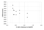
- Example 4 In Experiment 4, the condition of the wafer used was different from Experiment 3 to verify the correlation between the lifetime value and the Fe-B concentration.
- Example 6 a p-type wafer (oxygen concentration 0.8 ⁇ 10 18 atoms / cm 3 , dopant (boron) concentration 3.7 ⁇ 10 14 atoms / cm 3 , pulling rate 1.5 mm / min) is used. According to this embodiment, RTO film formation and corona charge passivation were performed to measure the lifetime, and the Fe-B concentration was determined by the SPV method.
- Example 6 The results of Example 6 are shown in the graph of FIG. In the graph of FIG. 8, the vertical axis is the lifetime value, and the horizontal axis is the Fe-B concentration. As shown in the graph of FIG. 8, in Example 6, no correlation was found between the lifetime value and the Fe-B concentration. In addition, the lifetime was reduced due to oxygen and holes, which was considered to be because the single crystal pulling up speed was too fast, 1.5 mm / min.
- Equation (1) when the calculated lifetime value is ⁇ , ⁇ b is the bulk lifetime and ⁇ s is the surface recombination lifetime.
- equation (2) for obtaining the bulk lifetime ⁇ b uses the equation of Shockley lead hole.
- n 0 and p 0 are carrier concentrations of electrons and holes at equilibrium
- ⁇ n and ⁇ p are injected carrier concentrations
- th th is the thermal velocity of carriers
- n i is the intrinsic carrier concentration
- Ei is the intrinsic energy standard
- ⁇ n and ⁇ p are capture cross sections for impurities electrons and holes
- N t is impurity carrier concentration
- E t impurity energy level
- k Boltzmann's constant
- T temperature.
- the impurity was assumed to be Fe, the level (E t ) was 0.4 eV, and the capture cross section ⁇ n was assumed to be 3.6 ⁇ 10 -15 cm 2 .
- the dopant (phosphorus) concentration n 0 of the wafer is 1 ⁇ 10 14 atoms / cm 3 and the temperature (T) is 300K.
- the injection carriers ⁇ n and ⁇ p are determined by using a laser of 904 nm and injecting 5 ⁇ 10 13 / cm 2 when lifetime measurement is performed by the ⁇ PCD apparatus in the standard mode. It becomes a value divided by 775 ⁇ m).
- S is the surface recombination velocity.
- tau dif the diffusion term in the front and back surfaces of the surface recombination lifetime
- tau sr recombination term in the front and back surfaces
- the Fe contamination concentration can be obtained with high accuracy by obtaining the measured value of the lifetime by the metal contamination evaluation method according to the present invention.
- Example 6 the growth conditions of the single crystal cut out from the silicon wafer used in the metal contamination evaluation method according to the present invention were further verified. Specifically, it verified about the range of a suitable pulling up rate and the range of oxygen concentration. In this experiment, conditions of single crystal pulling rate and oxygen concentration were set as shown in Table 1, and RTO film formation and corona charge passivation were performed for Examples 12 to 26, and lifetime measurement was performed using a ⁇ PCD apparatus. .
- the P type 36 ⁇ ⁇ cm, the dopant concentration boron 3.7 ⁇ 10 14 / cm 3 , the crystal part from which the wafer is cut out is the central part of the crystal with a total length of 1000 mm or more, and the conditions of the RTP apparatus are oxygen atmosphere.
- the temperature was lowered to 120 ° C./s at 1350 ° C. ⁇ 30 sec, to 600 ° C.
- the lifetime average value (lifetime in-plane average value) in the wafer surface obtained from the example under each condition is 3800 ⁇ sec, where the theoretical lifetime value (called ⁇ SRH ) estimated from the dopant concentration is 3800 ⁇ sec, It was considered as a rejection (decision x in Table 1) when it was less than 50% (1900 ⁇ sec) of ⁇ SRH , and was passed (decision ⁇ in Table 1) when it was 50% or more.
- Example 7 In Experiment 7, the conditions of the cutout position were set in Examples 27 to 35 in order to specify the position where the wafer was cut out from the single crystal, and evaluation was performed on the in-plane average value in the same manner as Experiment 6. Table 2 shows the conditions and experimental results of Examples 27 to 35.
- the pulling rate is 0.6 mm / min
- the oxygen concentration is 1.2 ⁇ 10 18 / cm 3
- the other conditions are the same as in Experiment 6.
- the pulling rate of silicon single crystal is 1.0 mm / min or less
- oxygen concentration is 1.3 ⁇ 10 18 / cm 3 or less
- the crystal site from which the wafer is cut is 40 mm from the head and 40 mm from the tail
- the reduction of the lifetime due to the vacancy type can be suppressed, and the metal contamination amount can be accurately evaluated by the lifetime measurement due to the metal contamination.
Abstract
The present invention addresses the problem of highly accurately measuring and evaluating the quantity of metal contamination to a silicon wafer in a high-speed heat treatment device. The present invention is provided with: a step for obtaining a silicon single crystal 10 having an oxygen concentration of 1.3×10¹⁸/cm3 or lower by growing the silicon single crystal at a pulling speed of 1.0 mm/min or lower by means of the Czochralski method; a step for cutting out a silicon wafer from a region excluding a region 40 mm to the center side from the head of the silicon single crystal, and a region 40 mm to the center side from the tail; a step for heat treating the silicon wafer by means of a high-speed heat treatment device, and thermally transferring, to the silicon wafer, a contaminant generated from members in a furnace; and a step for measuring a lifetime with respect to the silicon wafer, to which the contaminant is transferred.
Description
本発明は、金属汚染評価方法に関し、特に、シリコンウェーハを高速加熱処理する高速熱処理装置(RTP装置)において、炉内の金属汚染を精度良く評価することのできる金属汚染評価方法に関する。
The present invention relates to a method for evaluating metal contamination, and more particularly, to a method for evaluating metal contamination that can accurately evaluate metal contamination in a furnace in a rapid thermal processing apparatus (RTP apparatus) that heats a silicon wafer at high speed.
シリコンウェーハの製造過程、或いはデバイスの製造工程において、ウェーハが金属不純物などで汚染されると、製品性能に悪影響が生じる。そのため、金属汚染を低減することは、極めて重要な課題である。
Contamination of the wafer with metal impurities or the like in the silicon wafer manufacturing process or device manufacturing process adversely affects product performance. Therefore, reducing metal contamination is an extremely important issue.
この課題に対し、例えば特許文献1(特開2013-84840号公報)、特許文献2(特開2009-302337号公報)には、高抵抗のシリコンウェーハを熱処理炉において処理することによって金属汚染を該シリコンウェーハに転写し、その後SPV法(表面光起電力法)によるFe-B濃度検出や、μPCD法(マイクロ波光導電減衰法)によるライフタイム測定によって金属不純物の検出を行うことが開示されている。
To address this issue, for example, Patent Document 1 (Japanese Patent Application Laid-Open No. 2013-84840) and Patent Document 2 (Japanese Patent Application Laid-Open No. 2009-302337) disclose metal contamination by treating a high resistance silicon wafer in a heat treatment furnace. It is disclosed that metal impurities are detected by transferring to the silicon wafer and then detecting the Fe-B concentration by the SPV method (surface photovoltaic method) and measuring the lifetime by the μPCD method (microwave photoconductivity decay method). .
ところで、炉内における金属不純物の影響を確認するためには、特許文献1、2に開示されるように、熱処理においてシリコンウェーハ中に十分に金属不純物が拡散するように所定の温度で時間をかける必要がある。
しかしながら、特に熱処理炉が高速熱処理装置(RTP装置)である場合には、金属汚染ではなく、空孔起因によるライフタイムの低下が生じるため、金属不純物の汚染を正しく評価することが困難となっていた。 By the way, in order to confirm the influence of the metal impurities in the furnace, as disclosed in Patent Documents 1 and 2, it takes time at a predetermined temperature so that the metal impurities are sufficiently diffused in the silicon wafer in the heat treatment. There is a need.
However, particularly when the heat treatment furnace is a high-speed heat treatment apparatus (RTP apparatus), not a metal contamination but a decrease in lifetime due to pores occurs, so it is difficult to correctly evaluate the contamination of metal impurities. The
しかしながら、特に熱処理炉が高速熱処理装置(RTP装置)である場合には、金属汚染ではなく、空孔起因によるライフタイムの低下が生じるため、金属不純物の汚染を正しく評価することが困難となっていた。 By the way, in order to confirm the influence of the metal impurities in the furnace, as disclosed in
However, particularly when the heat treatment furnace is a high-speed heat treatment apparatus (RTP apparatus), not a metal contamination but a decrease in lifetime due to pores occurs, so it is difficult to correctly evaluate the contamination of metal impurities. The
また、ライフタイムの測定では表面再結合によるライフタイムの低下が起こる。その低下を抑制するには表面に保護膜としてのパシベーション膜を形成することが必要である。具体的なパシベーション手法としては、主に熱酸化やHF(フッ酸)パシベーション手法が知られている。熱酸化は、加熱によりシリコン酸化膜(熱酸化膜)をシリコン表面に形成し、良好なSi-SiO2界面を導入することにより表面パシベーション効果を得るものである。また、HFパシベーション手法は、HF(フッ酸)水溶液を用いたケミカルパシベーションである。
Also, in the measurement of lifetime, the lifetime decreases due to surface recombination. In order to suppress the decrease, it is necessary to form a passivation film as a protective film on the surface. As specific passivation methods, thermal oxidation and HF (hydrofluoric acid) passivation methods are mainly known. In thermal oxidation, a silicon oxide film (thermal oxide film) is formed on a silicon surface by heating, and a good Si—SiO 2 interface is introduced to obtain a surface passivation effect. The HF passivation method is chemical passivation using an aqueous solution of HF (hydrofluoric acid).
しかしながら、前記熱酸化による手法では、熱酸化膜を形成する熱処理炉からの汚染が考えられるため、目的とするRTP装置の汚染管理には使用できないという課題があった。
また、HFパシベーションにあっては、熱履歴を与えることはないが、表面再結合速度が20~40cm/sであることから、長いライフタイムを得ることが難しく、汚染管理としては感度の点で問題があった。 However, in the method by the above-mentioned thermal oxidation, since the contamination from the heat treatment furnace which forms a thermal oxide film can be considered, there existed a problem that it could not use for the contamination control of the target RTP apparatus.
In addition, although there is no thermal history in HF passivation, it is difficult to obtain a long lifetime because the surface recombination rate is 20 to 40 cm / s, and it is difficult to control contamination in terms of sensitivity. There was a problem.
本発明は、前記したような事情の下になされたものであり、高速熱処理装置におけるシリコンウェーハへの金属汚染量を高精度に測定し評価することのできる金属汚染評価方法を提供することを目的とする。
The present invention has been made under the circumstances as described above, and it is an object of the present invention to provide a metal contamination evaluation method capable of measuring and evaluating the amount of metal contamination on a silicon wafer in a high speed heat treatment apparatus with high accuracy. I assume.
前記課題を解決するためになされた、本発明に係る金属汚染評価方法は、高速熱処理装置におけるシリコンウェーハへの金属汚染量を測定する金属汚染評価方法であって、チョクラルスキー法により1.0mm/min以下の引き上げ速度で育成し、酸素濃度が1.3×1018/cm3以下のシリコン単結晶を得るステップと、前記シリコン単結晶のヘッドから中央側へ40mmとテイルから中央側へ40mmを除く領域からシリコンウェーハを切り出すステップと、前記シリコンウェーハを高速熱処理装置により熱処理し、炉内部材からの汚染物質を前記シリコンウェーハに熱転写させるステップと、汚染物質が転写された前記シリコンウェーハに対しライフタイム測定するステップと、を備えることに特徴を有する。
The metal contamination evaluation method according to the present invention, which was made to solve the above problems, is a metal contamination evaluation method for measuring the amount of metal contamination on a silicon wafer in a high-speed heat treatment apparatus, and is 1.0 mm by the Czochralski method. Step of growing silicon single crystal having an oxygen concentration of 1.3 × 10 18 / cm 3 or less by growing at a pulling rate of less than 1 / min, and 40 mm from the head of the silicon single crystal and 40 mm from the tail to the center Cutting out the silicon wafer from the region excluding the heat treatment, heat-treating the silicon wafer with a high-speed heat treatment apparatus, and thermally transferring the contaminants from the furnace inner member onto the silicon wafer, and with respect to the silicon wafer to which the contaminants are transferred. And measuring the lifetime.
尚、前記シリコンウェーハを高速熱処理装置により熱処理し、炉内部材からの汚染物質を前記シリコンウェーハに熱転写させるステップにおいて、酸化性ガス下で1100℃以上シリコン融点以下の温度で1乃至60sec保持した後、5乃至150℃/secの速度で降温処理し、前記シリコンウェーハ上に膜厚2nm以上の酸化膜を形成することが望ましい。
また、前記汚染物質が転写された前記シリコンウェーハに対しライフタイム測定するステップにおいて、前記シリコンウェーハに対しコロナチャージをパシベーションとして用いた後、ライフタイム測定することが望ましい。 Incidentally, in the step of heat-treating the silicon wafer with a high-speed heat treatment apparatus and thermally transferring the contaminants from the internal members to the silicon wafer, after holding for 1 to 60 seconds at a temperature of 1100 ° C. or more and silicon melting point or less under oxidizing gas. Preferably, the temperature is lowered at a rate of 5 to 150 ° C./sec to form an oxide film having a thickness of 2 nm or more on the silicon wafer.
In the step of measuring the lifetime of the silicon wafer to which the contaminant has been transferred, it is preferable to measure the lifetime after corona charge is used as passivation for the silicon wafer.
また、前記汚染物質が転写された前記シリコンウェーハに対しライフタイム測定するステップにおいて、μPCD装置を用いてライフタイム測定することが望ましい。
また、前記チョクラルスキー法により1.0mm/min以下の引き上げ速度で育成し、酸素濃度が1.3×1018/cm3以下のシリコン単結晶を得るステップにおいて、ドーパント濃度を5×1014atoms/cm3以下とすることが望ましい。
また、前記汚染物質が転写された前記シリコンウェーハに対しライフタイム測定するステップの後、金属不純物の濃度をyとし、ライフタイム値をxとすると、下記式のxに前記測定したライフタイム値を代入し、金属不純物の濃度yを求めるステップを備えることが望ましい。
[数2]
y=-4E+07・x+2E+11 Further, in the step of measuring the lifetime of the silicon wafer to which the contaminant has been transferred, it is desirable to measure the lifetime using a μPCD apparatus.
In addition, in the step of growing the silicon single crystal having an oxygen concentration of 1.3 × 10 18 / cm 3 or less by growing it at a pulling rate of 1.0 mm / min or less by the Czochralski method, the dopant concentration is 5 × 10 14. It is desirable to set atoms / cm 3 or less.
Also, after the step of measuring the lifetime of the silicon wafer to which the contaminant has been transferred, assuming that the concentration of metal impurities is y and the lifetime value is x, the lifetime value measured in x in the following equation is It is desirable to include the step of substituting and determining the concentration y of metal impurities.
[Equation 2]
y = -4E + 07 x 2E + 11
このような方法によれば、ウェーハ内部の酸素や格子欠陥による空孔型起因のライフタイム低下を減らし、金属不純物によるライフタイム低下の影響を精度良く評価することができる。
According to such a method, it is possible to reduce the decrease in lifetime caused by the vacancy type due to oxygen and lattice defects inside the wafer, and to accurately evaluate the influence of the decrease in lifetime due to the metal impurities.
本発明によれば、高速熱処理装置におけるシリコンウェーハへの金属汚染量を高精度に測定し評価することのできる金属汚染評価方法を提供することができる。
According to the present invention, it is possible to provide a metal contamination evaluation method capable of measuring and evaluating the amount of metal contamination on a silicon wafer in a high-speed heat treatment apparatus with high accuracy.
以下、本発明に係る金属汚染評価方法について説明する。
本発明の金属汚染評価方法にあっては、高速熱処理装置(以下、RTP装置とも呼ぶ)における金属汚染を評価するための方法である。具体的には、所定の育成条件により引き上げられたシリコン単結晶からシリコンウェーハを切り出し、RTP装置において所定の温度の酸化性雰囲気下で熱処理することによりウェーハ上にRTO(急速熱酸化)膜を形成する。
そして、RTP装置を構成する部材からの汚染物質をウェーハへ熱転写させ、このウェーハに対しコロナチャージを用いたパシベーション処理を行う。このようにして得られたウェーハのライフタイムを測定することによって、炉内の金属汚染検出を行う。 Hereinafter, the metal contamination evaluation method according to the present invention will be described.
The metal contamination evaluation method of the present invention is a method for evaluating metal contamination in a high-speed heat treatment apparatus (hereinafter also referred to as an RTP apparatus). Specifically, an RTO (rapid thermal oxidation) film is formed on a wafer by cutting a silicon wafer from a silicon single crystal pulled up under a predetermined growth condition, and heat treating it in an oxidizing atmosphere at a predetermined temperature in an RTP apparatus. Do.
Then, the contaminants from the members constituting the RTP apparatus are thermally transferred to the wafer, and the wafer is subjected to passivation processing using corona charge. The metal contamination in the furnace is detected by measuring the lifetime of the wafer thus obtained.
より具体的には、図1に示すフローのようになる。
先ずは金属汚染評価用のシリコンウェーハを切り出すためのシリコン単結晶を育成する(図1のステップS1)。
即ち、前記単結晶は、チョクラルスキー法により、酸素濃度が1.3×10¹⁸atoms/cm3(oldASTM)以下、ドーパント濃度5×1014atoms/cm3以下、引上げ速度が1mm/min以下の条件で引き上げられる。 More specifically, it becomes like the flow shown in FIG.
First, a silicon single crystal for growing a silicon wafer for metal contamination evaluation is grown (Step S1 in FIG. 1).
That is, according to the Czochralski method, the single crystal has an oxygen concentration of 1.3 × 10 18 atoms / cm 3 (old ASTM) or less, a dopant concentration of 5 × 10 14 atoms / cm 3 or less, and a pulling rate of 1 mm / min or less It is pulled up on condition of.
尚、ドーパント濃度が5×10¹⁴atoms/cm3以下の場合、即ち基板抵抗が高いと、ライフタイム評価において、多数キャリアのウェーハ表面での再結合影響が表れやすくなるため、ライフタイムの真値が得られにくくなる。しかしながら、本発明の金属汚染評価方法にあっては、表面再結合の影響が小さいため、ドーパント濃度が5×1014atoms/cm3以下であっても、精度良く金属汚染を評価することができる。
If the dopant concentration is 5 × 10 14 atoms / cm 3 or less, that is, if the substrate resistance is high, the effect of recombination of majority carriers on the wafer surface tends to appear in lifetime evaluation, so the true value of the lifetime is Is difficult to obtain. However, in the metal contamination evaluation method of the present invention, metal contamination can be accurately evaluated even if the dopant concentration is 5 × 10 14 atoms / cm 3 or less because the influence of surface recombination is small. .
そして、図2に示すように、引き上げられた単結晶インゴット10において、低温での熱履歴を長く受ける直胴部10bのヘッドショルダー10a側から中央側に40mmの位置10b1まで、及びテールコーン10c側から中央側に40mmの位置10b2までを除く領域(使用する領域)からシリコンウェーハを切り出す(図1のステップS2)。
この領域外が適用できない理由は、該領域外では結晶中の熱がインゴットの上下から放熱され(結晶が冷え易い)、V濃度(ベーカンシー(空孔)濃度)が高いまま空孔型欠陥の形成温度帯に入るため、結果として空孔型欠陥の濃度が高くなりライフタイムが低下するためである。 Then, as shown in FIG. 2, in the pulledsingle crystal ingot 10, the straight body portion 10b receiving a long heat history at low temperature from the head shoulder 10a side to the center side 40 mm position 10b1, and the tail cone 10c side A silicon wafer is cut out from the area (area to be used) except for the position 10b2 of 40 mm on the central side from the center of the silicon wafer (step S2 in FIG. 1).
The reason why the outside of this region can not be applied is that the heat in the crystal is dissipated from the top and bottom of the ingot outside this region (the crystal tends to cool) and the formation of vacancy type defects while the V concentration (Bacansee (vacancy) concentration) remains high. Since the temperature range is reached, the concentration of the vacancy defects increases as a result, and the lifetime decreases.
この領域外が適用できない理由は、該領域外では結晶中の熱がインゴットの上下から放熱され(結晶が冷え易い)、V濃度(ベーカンシー(空孔)濃度)が高いまま空孔型欠陥の形成温度帯に入るため、結果として空孔型欠陥の濃度が高くなりライフタイムが低下するためである。 Then, as shown in FIG. 2, in the pulled
The reason why the outside of this region can not be applied is that the heat in the crystal is dissipated from the top and bottom of the ingot outside this region (the crystal tends to cool) and the formation of vacancy type defects while the V concentration (Bacansee (vacancy) concentration) remains high. Since the temperature range is reached, the concentration of the vacancy defects increases as a result, and the lifetime decreases.
また、前記結晶部位の制限以外にも、上記のような酸素濃度、引上げ速度等の制限は、ライフタイム低下を引き起こす空孔型欠陥の形成影響による。空孔型欠陥の実体は明らかになっていないが、形態としては、VO、VO2(V:ベーカンシー(空孔)、O:酸素)などの複合体であると考えられる。また、このような空孔型欠陥の形成温度帯は、結晶の冷却過程において1000℃~800℃付近であると考えられる。
Further, in addition to the limitation of the crystal site, the limitation of the oxygen concentration, the pulling rate, etc. as described above is due to the formation effect of the vacancy type defect which causes the lifetime to decrease. Although the substance of the vacancy-type defect has not been clarified, the form is considered to be a complex of VO, VO 2 (V: Bacansee (pore), O: oxygen). In addition, the formation temperature zone of such a vacancy type defect is considered to be around 1000 ° C. to 800 ° C. in the cooling process of the crystal.
また、チョクラルスキー結晶の固液界面において熱平衡濃度で結晶中に取り込まれたV(空孔)とI(格子間Si)は、結晶の冷却過程において、対消滅して濃度低下していく。空孔型欠陥起因のライフタイム低下を回避するためには、V濃度を下げる必要があるが、引上げ速度が1mm/minを超える場合、V濃度が高いまま空孔型欠陥の形成温度帯に入るため、結果として空孔型欠陥の濃度が高くなりライフタイムが低下する。
また、酸素濃度が高いと空孔型欠陥の形成を助長するため、酸素濃度は1.3×10¹⁸atoms/cm3(oldASTM)以下が望ましい。 Further, V (voids) and I (interstitial Si) taken into the crystal at a thermal equilibrium concentration at the solid-liquid interface of the Czochralski crystal are annihilated in the process of cooling the crystal, and the concentration decreases. In order to avoid the lifetime reduction due to the vacancy type defect, it is necessary to lower the V concentration, but when the pulling speed exceeds 1 mm / min, the V concentration remains high and it enters the formation temperature zone of the vacancy type defect As a result, the concentration of vacancy defects increases and the lifetime decreases.
In addition, the oxygen concentration is preferably 1.3 × 10 18 atoms / cm 3 (old ASTM) or less in order to promote formation of vacancy-type defects when the oxygen concentration is high.
次いで、RTP装置により前記シリコンウェーハに対し、酸化性雰囲気下、1100℃以上シリコン融点以下で、1~60sec保持する。その後、5~150℃/secで降温処理を行い、シリコンウェーハ上に膜厚2nm以上の酸化膜(RTO膜)を形成する(図1のステップS3)。
Next, the silicon wafer is held by an RTP apparatus in an oxidizing atmosphere at a temperature of 1100 ° C. or more and a silicon melting point or less for 1 to 60 seconds. Thereafter, the temperature is lowered at 5 to 150 ° C./sec to form an oxide film (RTO film) having a film thickness of 2 nm or more on the silicon wafer (Step S3 in FIG. 1).
このRTP処理装置にあっては、より高い温度で使用することにより装置を構成する部材に存在する金属不純物の外方拡散を促進する。それにより炉内金属不純物をウェーハへ十分に転写することができる。
尚、一般的にウェーハ内の酸素や空孔がRTP処理によって電気的に活性状態となるため、それがライフタイムを低下させる要因となる。しかしながら、前記ステップS1の条件により得られたシリコンウェーハによれば、酸素や空孔が略無いため空孔型起因のライフタイムの低下を抑制し、金属不純物に従うライフタイム低下のみを測定することができる。 In this RTP processor, the use at higher temperatures promotes the outward diffusion of metal impurities present in the members constituting the device. Thereby, the metal impurities in the furnace can be sufficiently transferred to the wafer.
In general, oxygen and vacancies in the wafer are electrically activated by the RTP process, which causes a decrease in lifetime. However, according to the silicon wafer obtained under the condition of step S1, it is possible to suppress the decrease of the lifetime due to the vacancy type because there is almost no oxygen or the vacancy, and to measure only the lifetime decrease according to the metal impurities. it can.
そして、前記シリコンウェーハをコロナチャージのパシベーションとして用いたμPCD法によりライフタイム測定する(図1のステップS4)。
前記コロナチャージ処理においては、大気中で電荷を発生、制御する。このコロナチャージ処理により、シリコンウェーハ表面の電荷状態を制御して均一にすることができる。 Then, the lifetime is measured by the μPCD method using the silicon wafer as passivation of corona charge (step S4 in FIG. 1).
In the corona charging process, charge is generated and controlled in the atmosphere. By this corona charging process, the charge state of the silicon wafer surface can be controlled and made uniform.
μPCD測定装置としては、例えばコベルコ科研社製LTA-2200EPを用い、レーザ波長904nm、キャリア注入量5×10¹³/cm3、4mmピッチでライフタイム測定する。このμPCD法にあっては、シリコンウェーハに対しレーザ光をパルス照射することによって過剰キャリアが生成され、それが再結合により消滅して元の平衡状態に戻っていく。このときの過剰キャリア密度の変化は、光照射領域の抵抗率の指数関数的な変化となり、反射マイクロ波のパワーもそれに伴い変化する。光パルスの照射前と照射直後の反射マイクロ波パワーの差が抵抗率の差、即ちキャリア密度の差に対応し、その時間変化からライフタイムが求められる。
As a μPCD measuring apparatus, for example, using LTA-2200EP manufactured by Kobelco Research Institute, the lifetime is measured at a laser wavelength of 904 nm, a carrier injection amount of 5 × 10 13 / cm 3 and a 4 mm pitch. In this μPCD method, excess carriers are generated by applying a pulse to a silicon wafer with a laser beam, which disappears by recombination and returns to the original equilibrium state. The change in the excess carrier density at this time is an exponential change in the resistivity of the light irradiation area, and the power of the reflected microwave also changes accordingly. The difference in reflected microwave power before and after the light pulse irradiation corresponds to the difference in resistivity, ie, the difference in carrier density, and the lifetime is determined from the time change.
以上のように本発明に係る実施の形態によれば、酸素濃度が1.3×10¹⁸atoms/cm3(oldASTM)以下、引上げ速度が1mm/min以下の条件により育成されたシリコン単結晶から切り出されたウェーハを用い、1100℃以上融点以下の高温下におけるRTP処理を酸化性雰囲気で実施することによりRTO膜を形成し、RTP装置部材からの汚染物質をウェーハへ熱転写させ、このウェーハをコロナチャージパシベーション処理してμPCD法によりライフタイム測定するものである。
これにより、ウェーハ内部の酸素や格子欠陥による空孔型起因のライフタイム低下を減らし、金属不純物によるライフタイム低下の影響を評価することができる。
また、本発明の方法によれば、ドーパント濃度に関わらず精度良い測定が可能であるため、多数キャリアのウェーハ表面での再結合の影響が表れるドーパント濃度5×10¹⁴atoms/cm3以下の場合にも有効である。 As described above, according to the embodiment of the present invention, the silicon single crystal grown under the conditions of oxygen concentration of 1.3 × 10 18 atoms / cm 3 (old ASTM) or less and pulling speed of 1 mm / min or less An RTO film is formed by performing RTP processing in an oxidizing atmosphere at a high temperature of 1100 ° C. or more and a melting point or less using the cut-out wafer to thermally transfer the contaminants from the RTP device member to the wafer, and this wafer is corona-treated. The charge passivation process is performed to measure the lifetime by the μPCD method.
As a result, it is possible to reduce the decrease in lifetime caused by the vacancy type due to oxygen and lattice defects inside the wafer, and to evaluate the influence of the decrease in lifetime due to metal impurities.
Further, according to the method of the present invention, accurate measurement is possible regardless of the dopant concentration, and therefore, the case of the dopant concentration of 5 × 10 14 atoms / cm 3 or less where the influence of recombination of majority carriers on the wafer surface appears It is also effective.
尚、前記実施の形態においては、パシベーションにコロナチャージを用いたが、本発明の金属汚染評価方法にあっては、それに限定されるものではなく、他のパシベーション手法を行うシリコンウェーハに対しても適用することができる。
また、ライフタイム測定においては、μPCD装置を用いたが、本発明にあっては、それに限定されるものではなく、他の手法によりライフタイム測定してもよい。 Although corona charge is used for passivation in the above embodiment, the method for evaluating metal contamination according to the present invention is not limited to this, and it is also possible to use silicon wafers to which other passivation techniques are applied. It can apply.
Further, although the μPCD apparatus is used for measuring the lifetime, the present invention is not limited to this, and the lifetime may be measured by another method.
本発明に係る金属汚染評価方法について、実施例に基づきさらに説明する。本実施例では、前記実施の形態に基づき以下の実験を行った。
The metal contamination evaluation method according to the present invention will be further described based on examples. In the present example, the following experiment was performed based on the above embodiment.
(実験1)
実験1では、育成条件の異なるウェーハを用い、本実施の形態に示したライフタイム測定を行った。
実施例1では、酸素濃度0.8×10¹⁸atoms/cm3、ドーパント(ボロン)濃度7.8×1014atoms/cm3、引上速度0.6mm/minの条件で育成したPタイプ、抵抗17Ω・cmウェーハを用いた。 (Experiment 1)
InExperiment 1, using the wafers under different growth conditions, the lifetime measurement described in the present embodiment was performed.
In Example 1, P type grown under conditions of oxygen concentration 0.8 × 10 18 atoms / cm 3 , dopant (boron) concentration 7.8 × 10 14 atoms / cm 3 , and pulling speed 0.6 mm / min. A resistance 17 Ω · cm wafer was used.
実験1では、育成条件の異なるウェーハを用い、本実施の形態に示したライフタイム測定を行った。
実施例1では、酸素濃度0.8×10¹⁸atoms/cm3、ドーパント(ボロン)濃度7.8×1014atoms/cm3、引上速度0.6mm/minの条件で育成したPタイプ、抵抗17Ω・cmウェーハを用いた。 (Experiment 1)
In
In Example 1, P type grown under conditions of oxygen concentration 0.8 × 10 18 atoms / cm 3 , dopant (boron) concentration 7.8 × 10 14 atoms / cm 3 , and pulling speed 0.6 mm / min. A resistance 17 Ω · cm wafer was used.
実施例2では、酸素濃度0.8×10¹⁸atoms/cm3、ドーパント(ボロン)濃度3.7×1014atoms/cm3、引上速度1.5mm/minの条件で育成したPタイプ、抵抗36Ω・cmウェーハを用いた。
実施例3では、酸素濃度0.9×10¹⁸atoms/cm3、ドーパント(リン)濃度3.0×1013atoms/cm3、引上速度1.5mm/minの条件で育成したNタイプ、抵抗142Ω・cmのウェーハを用いた。 In Example 2, P type grown under conditions of oxygen concentration 0.8 × 10 18 atoms / cm 3 , dopant (boron) concentration 3.7 × 10 14 atoms / cm 3 and pulling speed 1.5 mm / min. A resistance 36 Ω · cm wafer was used.
In Example 3, N type grown under conditions of oxygen concentration 0.9 × 10 18 atoms / cm 3 , dopant (phosphorus) concentration 3.0 × 10 13 atoms / cm 3 , and pulling speed 1.5 mm / min. A wafer with a resistance of 142 Ω · cm was used.
実施例1~3において、RTP処理条件は同じく、1350℃×30sec処理後、600℃まで降温レート120℃/secで処理し、RTO膜を形成した。
また、いずれもμPCD測定装置(コベルコ科研社製LTA-2200EP)を用いて、レーザ波長904nm、キャリア注入量5×10¹³/cm3、4mmピッチでライフタイム測定した。 The same RTP processing conditions as in Examples 1 to 3 were performed at 1350 ° C. × 30 sec, and then processed at a temperature decrease rate of 120 ° C./sec up to 600 ° C. to form an RTO film.
Moreover, lifetime measurement was carried out at a laser wavelength of 904 nm, carrier injection amount of 5 × 10 13 / cm 3 and 4 mm pitch using a μPCD measurement apparatus (LTA-2200 EP manufactured by Kobelco Research Institute).
実施例1~3のライフタイム測定結果を図3、4、5にそれぞれ示す。図3、4、5は、ウェーハ面内におけるライフタイム値を色で区分けした分布図である。
実施例1の結果、ライフタイム平均値は1280μsecとなり、図3に示されるように、局所汚染や外周の汚染が認められた。これは、RTP処理時に、ウェーハ裏面の外周部をSiCリングで保持するため、そこからの汚染と考えられた。即ち、実施例1の条件のウェーハを用いた場合、金属汚染分布を精度良く把握できることが確認できた。 The lifetime measurement results of Examples 1 to 3 are shown in FIGS. FIGS. 3, 4 and 5 are distribution maps in which the lifetime values in the wafer plane are classified by color.
As a result of Example 1, the lifetime average value was 1280 μsec, and as shown in FIG. 3, local contamination and contamination of the outer periphery were recognized. This was considered to be contamination from the outer periphery of the back surface of the wafer held by the SiC ring during RTP processing. That is, when the wafer of the conditions of Example 1 was used, it has confirmed that metal contamination distribution could be grasped | ascertained precisely.
また、実施例2、3の結果、ライフタイム平均値は、ともに1080μsecとなり、図4、5にそれぞれ示されるように、空孔型欠陥起因のライフタイム低下が認められた。この空孔型欠陥起因のライフタイム低下は、ウェーハ全面で影響があるが、中心部ほど影響が大きい。これは、実施例2,3とも引上速度が1.5mm/minであり速すぎることが原因であると考えられた。
Moreover, as a result of Examples 2 and 3, the lifetime average values were both 1080 μsec, and as shown in FIGS. 4 and 5, respectively, the lifetime reduction due to the vacancy type defect was recognized. The lifetime reduction caused by the vacancy defects has an effect on the entire surface of the wafer, but the effect is greater at the central portion. This is considered to be caused by the pull-up speed of 1.5 mm / min in each of Examples 2 and 3, which is too fast.
(実験2)
実験2では、パシベーション方法の異なる実施例4(RTO膜+コロナチャージ)、比較例1(熱酸化膜)、比較例2(HFパシベーション)について、抵抗率に対するライフタイム測定値と、表面再結合速度との関係について検証した。
図6のグラフに、実施例4、比較例1、2の結果を示す。図6のグラフにおいて、縦軸はライフタイム値、横軸はPタイプウェーハの抵抗値である。また、図中に表面再結合速度S=5cm/s、10cm/s、20cm/s、40cm/sの曲線を示す。
また、表面再結合速度は、熱酸化ではS=20cm/s、HFパシベーションではS=20~40cm/s程度となった。それに対し実施例4では、表面再結合速度S=0cm/sに近い真のバルク値に近い長いライフタイム値を得ることができた。 (Experiment 2)
InExperiment 2, the lifetime measurement values for the resistivity, and the surface recombination velocity for Example 4 (RTO film + corona charge), Comparative example 1 (thermal oxide film) and Comparative example 2 (HF passivation) different in passivation method. It verified about the relation with.
The graph of FIG. 6 shows the results of Example 4 and Comparative Examples 1 and 2. In the graph of FIG. 6, the vertical axis is the lifetime value, and the horizontal axis is the resistance value of the P-type wafer. Also, curves of surface recombination velocity S = 5 cm / s, 10 cm / s, 20 cm / s, and 40 cm / s are shown in the figure.
The surface recombination rate was about S = 20 cm / s for thermal oxidation and about S = 20 to 40 cm / s for HF passivation. On the other hand, in Example 4, a long lifetime value close to the true bulk value close to the surface recombination velocity S = 0 cm / s could be obtained.
実験2では、パシベーション方法の異なる実施例4(RTO膜+コロナチャージ)、比較例1(熱酸化膜)、比較例2(HFパシベーション)について、抵抗率に対するライフタイム測定値と、表面再結合速度との関係について検証した。
図6のグラフに、実施例4、比較例1、2の結果を示す。図6のグラフにおいて、縦軸はライフタイム値、横軸はPタイプウェーハの抵抗値である。また、図中に表面再結合速度S=5cm/s、10cm/s、20cm/s、40cm/sの曲線を示す。
また、表面再結合速度は、熱酸化ではS=20cm/s、HFパシベーションではS=20~40cm/s程度となった。それに対し実施例4では、表面再結合速度S=0cm/sに近い真のバルク値に近い長いライフタイム値を得ることができた。 (Experiment 2)
In
The graph of FIG. 6 shows the results of Example 4 and Comparative Examples 1 and 2. In the graph of FIG. 6, the vertical axis is the lifetime value, and the horizontal axis is the resistance value of the P-type wafer. Also, curves of surface recombination velocity S = 5 cm / s, 10 cm / s, 20 cm / s, and 40 cm / s are shown in the figure.
The surface recombination rate was about S = 20 cm / s for thermal oxidation and about S = 20 to 40 cm / s for HF passivation. On the other hand, in Example 4, a long lifetime value close to the true bulk value close to the surface recombination velocity S = 0 cm / s could be obtained.
(実験3)
実験3では、ライフタイム値とFe-B濃度との相関について検証した。
実施例5では、p型ウェーハ(酸素濃度0.8×10¹⁸atoms/cm3、ドーパント濃度7.8×1014atoms/cm3、引上速度0.6mm/min)を用い、本実施の形態に従いRTO膜形成、コロナチャージパシベーションを行ってライフタイム測定し、SPV法によりFe-B濃度を求めた。
比較例3として、同条件で切り出したp型ウェーハを、HFパシベーションを行ってライフタイム測定し、SPV法によりFe-B濃度を求めた。 (Experiment 3)
In Experiment 3, the correlation between the lifetime value and the Fe-B concentration was verified.
In Example 5, a p-type wafer (oxygen concentration 0.8 × 10 18 atoms / cm 3 , dopant concentration 7.8 × 10 14 atoms / cm 3 , pulling rate 0.6 mm / min) was used. RTO film formation and corona charge passivation were performed according to the form, lifetime was measured, and the Fe-B concentration was determined by the SPV method.
As Comparative Example 3, a p-type wafer cut out under the same conditions was subjected to HF passivation, lifetime measurement was performed, and the Fe-B concentration was determined by the SPV method.
実施例5及び比較例3の結果を図7のグラフに示す。図7のグラフにおいて、縦軸はライフタイム値、横軸はFe-B濃度である。
図7のグラフに示すように、実施例5では、ライフタイム値とFe-B濃度との間に強い相関が見られた。一方、比較例3では、長いライフタイム値が得られないため、弱い相関となった。 The results of Example 5 and Comparative Example 3 are shown in the graph of FIG. In the graph of FIG. 7, the vertical axis is the lifetime value, and the horizontal axis is the Fe-B concentration.
As shown in the graph of FIG. 7, in Example 5, a strong correlation was observed between the lifetime value and the Fe-B concentration. On the other hand, in Comparative Example 3, a long correlation was not obtained because a long lifetime value could not be obtained.
(実験4)
実験4では、実験3とは使用するウェーハ条件を変えて、ライフタイム値とFe-B濃度との相関について検証した。
実施例6では、p型ウェーハ(酸素濃度0.8×10¹⁸atoms/cm3、ドーパント(ボロン)濃度3.7×1014atoms/cm3、引上速度1.5mm/min)を用い、本実施の形態に従いRTO膜形成、コロナチャージパシベーションを行ってライフタイム測定し、SPV法によりFe-B濃度を求めた。 (Experiment 4)
In Experiment 4, the condition of the wafer used was different from Experiment 3 to verify the correlation between the lifetime value and the Fe-B concentration.
In Example 6, a p-type wafer (oxygen concentration 0.8 × 10 18 atoms / cm 3 , dopant (boron) concentration 3.7 × 10 14 atoms / cm 3 , pulling rate 1.5 mm / min) is used. According to this embodiment, RTO film formation and corona charge passivation were performed to measure the lifetime, and the Fe-B concentration was determined by the SPV method.
実施例6の結果を図8のグラフに示す。図8のグラフにおいて、縦軸はライフタイム値、横軸はFe-B濃度である。
図8のグラフに示すように、実施例6では、ライフタイム値とFe-B濃度との間に相関は見られなかった。また、酸素、空孔起因のライフタイム低下となり、これは、単結晶引上速度が1.5mm/minと速すぎるためと考えられた。 The results of Example 6 are shown in the graph of FIG. In the graph of FIG. 8, the vertical axis is the lifetime value, and the horizontal axis is the Fe-B concentration.
As shown in the graph of FIG. 8, in Example 6, no correlation was found between the lifetime value and the Fe-B concentration. In addition, the lifetime was reduced due to oxygen and holes, which was considered to be because the single crystal pulling up speed was too fast, 1.5 mm / min.
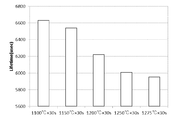
(実験5)
実験5では、熱処理温度の違いによりウェーハに転写される金属汚染量の差を本発明によるライフタイム測定により検出可能か検証した。
本実験では、n型ウェーハ(酸素濃度1.2×10¹⁸atoms/cm3、ドーパント(リン)濃度1×1014atoms/cm3、引上速度0.5mm/min)を用いた。RTP装置において、実施例7では1100℃×30sec、実施例8では1150℃×30sec、実施例9では1200℃×30sec、実施例10では1250℃×30sec、実施例11では1275℃×30secで熱処理を行い、RTO膜を形成した。その後、コロナチャージパシベーションを行い、μPCD装置によりライフタイム測定を行った。 (Experiment 5)
In Experiment 5, it was verified whether the difference in the amount of metal contamination transferred to the wafer due to the difference in the heat treatment temperature could be detected by the lifetime measurement according to the present invention.
In this experiment, an n-type wafer (oxygen concentration 1.2 × 10 18 atoms / cm 3 , dopant (phosphorus)concentration 1 × 10 14 atoms / cm 3 , pulling rate 0.5 mm / min) was used. In the RTP apparatus, the heat treatment is performed at 1100 ° C. × 30 sec in Example 7, 1150 ° C. × 30 sec in Example 8, 1200 ° C. × 30 sec in Example 9, 1250 ° C. × 30 sec in Example 10, and 1275 ° C. × 30 sec in Example 11. To form an RTO film. Thereafter, corona charge passivation was performed, and lifetime measurement was performed by the μPCD apparatus.
実験5では、熱処理温度の違いによりウェーハに転写される金属汚染量の差を本発明によるライフタイム測定により検出可能か検証した。
本実験では、n型ウェーハ(酸素濃度1.2×10¹⁸atoms/cm3、ドーパント(リン)濃度1×1014atoms/cm3、引上速度0.5mm/min)を用いた。RTP装置において、実施例7では1100℃×30sec、実施例8では1150℃×30sec、実施例9では1200℃×30sec、実施例10では1250℃×30sec、実施例11では1275℃×30secで熱処理を行い、RTO膜を形成した。その後、コロナチャージパシベーションを行い、μPCD装置によりライフタイム測定を行った。 (Experiment 5)
In Experiment 5, it was verified whether the difference in the amount of metal contamination transferred to the wafer due to the difference in the heat treatment temperature could be detected by the lifetime measurement according to the present invention.
In this experiment, an n-type wafer (oxygen concentration 1.2 × 10 18 atoms / cm 3 , dopant (phosphorus)
実施例7~11の結果を図9の棒グラフに示す。このグラフから明らかなように、熱処理温度の違いにより、ウェーハに転写される金属汚染量の差をライフタイム測定により検出できることを確認した。
The results of Examples 7 to 11 are shown in the bar graph of FIG. As is clear from this graph, it was confirmed that the difference in the amount of metal contamination transferred to the wafer can be detected by lifetime measurement due to the difference in the heat treatment temperature.
また、実施例7~11の結果に基づき、ライフタイム値とFe-B濃度との相関を下記の式(1)~式(3)を用いて求めた。
Further, based on the results of Examples 7 to 11, the correlation between the lifetime value and the Fe-B concentration was determined using the following formulas (1) to (3).
尚、式(1)において、計算されるライフタイム値をτとすると、τbはバルクライフタイム、τsは表面再結合ライフタイムである。
また、バルクライフタイムτbを求める式(2)は、ショックレーリードホールの演算式を用いた。ここで、n0とp0は平衡時の電子とホールのキャリア濃度、ΔnとΔpは注入されたキャリア濃度、νthはキャリアの熱速度、niは真性キャリア濃度、Eiは真性エネルギー準位、σnとσpは不純物の電子とホールに対する捕獲断面積、Ntは不純物キャリア濃度、Etは不純物エネルギー準位、kはボルツマン定数、Tは温度である。 In equation (1), when the calculated lifetime value is τ, τ b is the bulk lifetime and τ s is the surface recombination lifetime.
Further, the equation (2) for obtaining the bulk lifetime τ b uses the equation of Shockley lead hole. Here, n 0 and p 0 are carrier concentrations of electrons and holes at equilibrium, Δ n and Δ p are injected carrier concentrations, th th is the thermal velocity of carriers, n i is the intrinsic carrier concentration, and Ei is the intrinsic energy standard , Σ n and σ p are capture cross sections for impurities electrons and holes, N t is impurity carrier concentration, E t is impurity energy level, k is Boltzmann's constant, and T is temperature.
不純物はFeと仮定し、準位(Et)を0.4eV、捕獲断面積σnを3.6×10⁻¹⁵cm2と仮定した。また、ウェーハのドーパント(リン)濃度n0は1×10¹⁴atoms/cm3、温度(T)は300Kと仮定した。平衡状態におけるキャリア濃度は、次式p0・n0=ni
2で表されることから、p0が決定する。注入キャリアΔnとΔpは、μPCD装置によるライフタイム測定をスタンダードモードでおこなった場合、904nmのレーザを使用して5×10¹³/cm2が注入されることから、これをウェーハ厚さ(t=775μm)で割った値となる。
The impurity was assumed to be Fe, the level (E t ) was 0.4 eV, and the capture cross section σ n was assumed to be 3.6 × 10 -15 cm 2 . In addition, it is assumed that the dopant (phosphorus) concentration n 0 of the wafer is 1 × 10 14 atoms / cm 3 and the temperature (T) is 300K. The carrier concentration in the equilibrium state is p 0 · n 0 = n i 2 because p 0 is determined. The injection carriers Δn and Δp are determined by using a laser of 904 nm and injecting 5 × 10 13 / cm 2 when lifetime measurement is performed by the μPCD apparatus in the standard mode. It becomes a value divided by 775 μm).
Sは表面再結合速度である。表面再結合ライフタイムτsを求める式(3)において、表面再結合ライフタイムの表裏面への拡散項(τdif)と表裏面での再結合の項(τsr)で現される。Dは少数キャリアの拡散係数、tはウェーハ厚さ、表面再結合速度Sを6cm/secと仮定した。
S is the surface recombination velocity. In the formula (3) to determine the surface recombination lifetime tau s, it is revealed in the diffusion term in the front and back surfaces of the surface recombination lifetime (tau dif) and recombination term in the front and back surfaces (tau sr). It is assumed that D is the diffusion coefficient of minority carriers, t is the wafer thickness, and the surface recombination velocity S is 6 cm / sec.
上記式(1)~(3)を用いて得られた結果(計算値)を図10のグラフに示す。図10において、縦軸(y軸)はFe濃度(atoms/cm3)、横軸(x軸)はライフタイム(μsec)である。
このグラフから、金属不純物であるFeの濃度(y軸)とライフタイム値(x軸)との間には、下記相関式(4)が得られた。 The results (calculated values) obtained using the above equations (1) to (3) are shown in the graph of FIG. In FIG. 10, the vertical axis (y axis) is the Fe concentration (atoms / cm 3 ), and the horizontal axis (x axis) is the lifetime (μsec).
From this graph, the following correlation equation (4) was obtained between the concentration (y axis) of Fe as a metal impurity and the lifetime value (x axis).
[数2]
y=-4E+07・x+2E+11 ・・・・(4) [Equation 2]
y = -4E + 07 x 2 E + 1 1 (4)
y=-4E+07・x+2E+11 ・・・・(4) [Equation 2]
y = -4E + 07 x 2 E + 1 1 (4)
即ち、本発明に係る金属汚染評価方法によりライフタイムの実測値を得ることにより、Fe汚染濃度を高精度に得ることができることを確認した。
That is, it was confirmed that the Fe contamination concentration can be obtained with high accuracy by obtaining the measured value of the lifetime by the metal contamination evaluation method according to the present invention.
(実験6)
実験6では、本発明に係る金属汚染評価方法に用いるシリコンウェーハを切り出す単結晶の育成条件について、更に検証した。具体的には、好適な引上速度の範囲と酸素濃度の範囲について検証した。
本実験では、実施例12~26について、単結晶引上速度と酸素濃度の条件を表1に示すように設定し、RTO膜形成、コロナチャージパシベーションを行い、μPCD装置によるライフタイム測定を行った。 (Experiment 6)
In Experiment 6, the growth conditions of the single crystal cut out from the silicon wafer used in the metal contamination evaluation method according to the present invention were further verified. Specifically, it verified about the range of a suitable pulling up rate and the range of oxygen concentration.
In this experiment, conditions of single crystal pulling rate and oxygen concentration were set as shown in Table 1, and RTO film formation and corona charge passivation were performed for Examples 12 to 26, and lifetime measurement was performed using a μPCD apparatus. .
実施例12~26において、Pタイプ36Ω・cm、ドーパント濃度ボロン3.7×10¹⁴/cm3、ウェーハを切り出す結晶部位を全長1000mm以上の結晶の中央部、RTP装置の条件は酸素雰囲気下で1350℃×30sec、600℃までの降温速度120℃/sとした。
また、ドーパント濃度から推定されるライフタイム理論値(τSRHと呼ぶ)を3800μsecとし、各条件での実施例から得られたウェーハ面内のライフタイム平均値(ライフタイム面内平均値)が、τSRHの50%(1900μsec)未満の場合に不合格(表1中の判定×)とし、50%以上の場合に合格(表1中の判定○)とした。 In Examples 12 to 26, the P type 36 Ω · cm, the dopant concentration boron 3.7 × 10 14 / cm 3 , the crystal part from which the wafer is cut out is the central part of the crystal with a total length of 1000 mm or more, and the conditions of the RTP apparatus are oxygen atmosphere. The temperature was lowered to 120 ° C./s at 1350 ° C. × 30 sec, to 600 ° C.
Further, the lifetime average value (lifetime in-plane average value) in the wafer surface obtained from the example under each condition is 3800 μsec, where the theoretical lifetime value (called τ SRH ) estimated from the dopant concentration is 3800 μsec, It was considered as a rejection (decision x in Table 1) when it was less than 50% (1900 μsec) of τ SRH , and was passed (decision ○ in Table 1) when it was 50% or more.
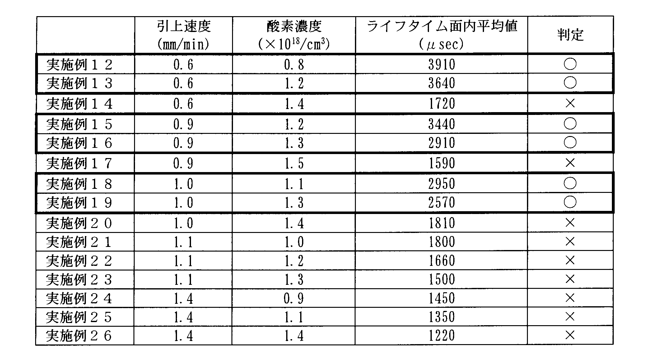
表1に示すように、引き上げ速度は1.0mm/min以下、酸素濃度は1.3×1018/cm3以下の場合に良い結果が得られた。
As shown in Table 1, good results were obtained when the pulling rate was 1.0 mm / min or less and the oxygen concentration was 1.3 × 10 18 / cm 3 or less.
(実験7)
実験7では、単結晶からウェーハを切り出す位置を特定するために実施例27~35において切り出し位置の条件を設定し、実験6と同様にライフタイム面内平均値について評価を行った。表2に実施例27~35の条件及び実験結果を示す。引上速度は0.6mm/min、酸素濃度は1.2×1018/cm3とし、その他の条件は実験6と同じである。 (Experiment 7)
In Experiment 7, the conditions of the cutout position were set in Examples 27 to 35 in order to specify the position where the wafer was cut out from the single crystal, and evaluation was performed on the in-plane average value in the same manner as Experiment 6. Table 2 shows the conditions and experimental results of Examples 27 to 35. The pulling rate is 0.6 mm / min, the oxygen concentration is 1.2 × 10 18 / cm 3 , and the other conditions are the same as in Experiment 6.

表2に示すように、結晶部位は、単結晶インゴッドのヘッドから40mmとテイルから40mmを除く領域から切り出したウェーハにおいて良好な結果が得られた。
As shown in Table 2, good results were obtained in the wafers cut out from the region excluding 40 mm from the head of the single crystal ingot and 40 mm from the tail as shown in Table 2.
以上の実施例の結果より、シリコン単結晶の引上速度が1.0mm/min以下、酸素濃度が1.3×1018/cm3以下、ウェーハを切り出す結晶部位がヘッドから40mmとテイルから40mmを除く領域の場合に空孔型起因のライフタイム低下を抑制し、金属汚染によるライフタイム測定により金属汚染量を精度良く評価出来ることを確認した。
According to the results of the above example, the pulling rate of silicon single crystal is 1.0 mm / min or less, oxygen concentration is 1.3 × 10 18 / cm 3 or less, and the crystal site from which the wafer is cut is 40 mm from the head and 40 mm from the tail In the case of the area excluding the above, it was confirmed that the reduction of the lifetime due to the vacancy type can be suppressed, and the metal contamination amount can be accurately evaluated by the lifetime measurement due to the metal contamination.
10 単結晶インゴッド
10 Single crystal ingot
Claims (6)
- 高速熱処理装置におけるシリコンウェーハへの金属汚染量を測定する金属汚染評価方法であって、
チョクラルスキー法により1.0mm/min以下の引き上げ速度で育成し、酸素濃度が1.3×1018/cm3以下のシリコン単結晶を得るステップと、
前記シリコン単結晶のヘッドから中央側へ40mmとテイルから中央側へ40mmを除く領域からシリコンウェーハを切り出すステップと、
前記シリコンウェーハを高速熱処理装置により熱処理し、炉内部材からの汚染物質を前記シリコンウェーハに熱転写させるステップと、
汚染物質が転写された前記シリコンウェーハに対しライフタイム測定するステップと、を備えることを特徴とする金属汚染評価方法。 A metal contamination evaluation method for measuring the amount of metal contamination on a silicon wafer in a rapid thermal processing apparatus, comprising:
A step of obtaining a silicon single crystal having an oxygen concentration of 1.3 × 10 18 / cm 3 or less by growing it at a pulling rate of 1.0 mm / min or less by the Czochralski method;
Cutting the silicon wafer from an area excluding 40 mm from the head of the silicon single crystal to the center side and 40 mm from the tail to the center side;
Heat treating the silicon wafer with a high speed heat treatment apparatus to thermally transfer the contaminants from the furnace internals to the silicon wafer;
Measuring the lifetime of the silicon wafer to which a contaminant has been transferred. - 前記シリコンウェーハを高速熱処理装置により熱処理し、炉内部材からの汚染物質を前記シリコンウェーハに熱転写させるステップにおいて、
酸化性ガス下で1100℃以上シリコン融点以下の温度で1乃至60sec保持した後、5乃至150℃/secの速度で降温処理し、前記シリコンウェーハ上に膜厚2nm以上の酸化膜を形成することを特徴とする請求項1に記載された金属汚染評価方法。 Heat-treating the silicon wafer by a high-speed heat treatment apparatus to thermally transfer the contaminants from the internal members to the silicon wafer;
After holding for 1 to 60 seconds at a temperature of 1100 ° C. or more and silicon melting point or less under an oxidizing gas, the temperature is lowered at a rate of 5 to 150 ° C./sec to form an oxide film with a film thickness of 2 nm or more on the silicon wafer. The metal contamination evaluation method described in Claim 1 characterized by these. - 前記汚染物質が転写された前記シリコンウェーハに対しライフタイム測定するステップにおいて、
前記シリコンウェーハに対しコロナチャージをパシベーションとして用いた後、ライフタイム測定することを特徴とする請求項1または請求項2に記載された金属汚染評価方法。 In the step of measuring the lifetime of the silicon wafer to which the contaminant has been transferred,
The method for evaluating metal contamination according to claim 1 or 2, wherein a lifetime is measured after corona charge is used as passivation for the silicon wafer. - 前記汚染物質が転写された前記シリコンウェーハに対しライフタイム測定するステップにおいて、
μPCD装置を用いてライフタイム測定することを特徴とする請求項1乃至請求項3のいずれかに記載された金属汚染評価方法。 In the step of measuring the lifetime of the silicon wafer to which the contaminant has been transferred,
The metal contamination evaluation method according to any one of claims 1 to 3, wherein the lifetime is measured using a μPCD apparatus. - 前記チョクラルスキー法により1.0mm/min以下の引き上げ速度で育成し、酸素濃度が1.3×1018/cm3以下のシリコン単結晶を得るステップにおいて、
ドーパント濃度を5×10¹⁴atoms/cm3以下とすることを特徴とする請求項1乃至請求項4のいずれかに記載された金属汚染評価方法。 In the step of growing a silicon single crystal having an oxygen concentration of 1.3 × 10 18 / cm 3 or less, which is grown at a pulling rate of 1.0 mm / min or less by the Czochralski method.
The metal contamination evaluation method according to any one of claims 1 to 4, wherein the dopant concentration is 5 x 10 14 atoms / cm 3 or less. - 前記汚染物質が転写された前記シリコンウェーハに対しライフタイム測定するステップの後、
金属不純物の濃度をyとし、ライフタイム値をxとすると、下記式のxに前記測定したライフタイム値を代入し、金属不純物の濃度yを求めるステップを備えることを特徴とする請求項1乃至請求項5のいずれかに記載された金属汚染評価方法。
[数2]
y=-4E+07・x+2E+11 After the step of measuring the lifetime of the silicon wafer to which the contaminant has been transferred,
Assuming that the metal impurity concentration is y and the lifetime value is x, the measured lifetime value is substituted into x in the following equation to obtain the metal impurity concentration y. The metal contamination evaluation method described in any one of Claim 5.
[Equation 2]
y = -4E + 07 x 2E + 11
Priority Applications (4)
| Application Number | Priority Date | Filing Date | Title |
|---|---|---|---|
| US16/956,282 US11538721B2 (en) | 2017-12-22 | 2018-08-02 | Evaluation method of metal contamination |
| KR1020207021032A KR102463966B1 (en) | 2017-12-22 | 2018-08-02 | Methods for Assessing Metal Contamination |
| CN201880082997.6A CN111480219A (en) | 2017-12-22 | 2018-08-02 | Method for evaluating metal contamination |
| EP18891783.5A EP3731263A4 (en) | 2017-12-22 | 2018-08-02 | Metal contamination evaluation method |
Applications Claiming Priority (2)
| Application Number | Priority Date | Filing Date | Title |
|---|---|---|---|
| JP2017246190A JP7057122B2 (en) | 2017-12-22 | 2017-12-22 | Metal pollution evaluation method |
| JP2017-246190 | 2017-12-22 |
Publications (1)
| Publication Number | Publication Date |
|---|---|
| WO2019123706A1 true WO2019123706A1 (en) | 2019-06-27 |
Family
ID=66994648
Family Applications (1)
| Application Number | Title | Priority Date | Filing Date |
|---|---|---|---|
| PCT/JP2018/029009 WO2019123706A1 (en) | 2017-12-22 | 2018-08-02 | Metal contamination evaluation method |
Country Status (7)
| Country | Link |
|---|---|
| US (1) | US11538721B2 (en) |
| EP (1) | EP3731263A4 (en) |
| JP (1) | JP7057122B2 (en) |
| KR (1) | KR102463966B1 (en) |
| CN (1) | CN111480219A (en) |
| TW (1) | TWI717628B (en) |
| WO (1) | WO2019123706A1 (en) |
Cited By (1)
| Publication number | Priority date | Publication date | Assignee | Title |
|---|---|---|---|---|
| WO2021162046A1 (en) * | 2020-02-14 | 2021-08-19 | グローバルウェーハズ・ジャパン株式会社 | Method for producing silicon single crystal |
Families Citing this family (1)
| Publication number | Priority date | Publication date | Assignee | Title |
|---|---|---|---|---|
| CN112908876A (en) * | 2021-01-18 | 2021-06-04 | 上海新昇半导体科技有限公司 | Silicon chip metal pollution testing method and device |
Citations (8)
| Publication number | Priority date | Publication date | Assignee | Title |
|---|---|---|---|---|
| JP2004189584A (en) * | 2002-10-18 | 2004-07-08 | Sumitomo Mitsubishi Silicon Corp | Method of measuring point defect distribution in silicon single crystal ingot |
| JP2009302337A (en) | 2008-06-13 | 2009-12-24 | Shin Etsu Handotai Co Ltd | Monitor wafer for contamination detection, contamination detection method, and method of manufacturing epitaxial wafer |
| JP2010177494A (en) * | 2009-01-30 | 2010-08-12 | Covalent Materials Corp | Method for heat treatment of silicon wafer |
| WO2010119614A1 (en) * | 2009-04-13 | 2010-10-21 | 信越半導体株式会社 | Anneal wafer, method for manufacturing anneal wafer, and method for manufacturing device |
| JP2013084840A (en) | 2011-10-12 | 2013-05-09 | Shin Etsu Handotai Co Ltd | Metal contamination evaluation method and epitaxial wafer manufacturing method |
| JP2013105914A (en) * | 2011-11-14 | 2013-05-30 | Shin Etsu Handotai Co Ltd | Vapor deposition device cleanliness evaluation method |
| JP2014058414A (en) * | 2012-09-14 | 2014-04-03 | Jnc Corp | Method for producing silicon single crystal for evaluation |
| JP2017103275A (en) * | 2015-11-30 | 2017-06-08 | 株式会社Sumco | Method for evaluating silicon wafer and use thereof |
Family Cites Families (15)
| Publication number | Priority date | Publication date | Assignee | Title |
|---|---|---|---|---|
| GB0216184D0 (en) | 2002-07-12 | 2002-08-21 | Aoti Operating Co Inc | Detection method and apparatus |
| AU2003301326A1 (en) | 2002-10-18 | 2004-05-04 | Sumitomo Mitsubishi Silicon Corporation | Method of measuring point defect distribution of silicon single crystal ingot |
| KR100500712B1 (en) * | 2002-12-16 | 2005-07-11 | 주식회사 실트론 | A method for measuring concentration of metal contamintion of silicon wafer |
| JP2009266835A (en) * | 2008-04-21 | 2009-11-12 | Sumco Corp | Metal contamination evaluating method of silicon single crystal |
| US8252700B2 (en) | 2009-01-30 | 2012-08-28 | Covalent Materials Corporation | Method of heat treating silicon wafer |
| JP5467923B2 (en) * | 2010-05-06 | 2014-04-09 | 信越半導体株式会社 | Manufacturing method of silicon wafer for metal contamination evaluation |
| JP5621612B2 (en) | 2011-01-19 | 2014-11-12 | 株式会社Sumco | Silicon single crystal inspection method and manufacturing method |
| JP5742742B2 (en) * | 2012-02-08 | 2015-07-01 | 信越半導体株式会社 | Metal contamination assessment method |
| JP5733245B2 (en) | 2012-03-16 | 2015-06-10 | 信越半導体株式会社 | Manufacturing method of silicon single crystal wafer |
| DE102012214085B4 (en) | 2012-08-08 | 2016-07-07 | Siltronic Ag | Single crystal silicon wafer and process for its production |
| CN108441940A (en) | 2013-01-08 | 2018-08-24 | Lg矽得荣株式会社 | Single crystal wafers, its manufacturing method and the method for detecting defect |
| EP2779220B1 (en) * | 2013-03-12 | 2017-10-25 | GLobalWafers Japan Co., Ltd. | Saturation voltage estimation method and silicon epitaxial wafer manufaturing method |
| JP5885305B2 (en) * | 2013-08-07 | 2016-03-15 | グローバルウェーハズ・ジャパン株式会社 | Silicon wafer and manufacturing method thereof |
| JP6044660B2 (en) | 2015-02-19 | 2016-12-14 | 信越半導体株式会社 | Silicon wafer manufacturing method |
| DE102015224983B4 (en) | 2015-12-11 | 2019-01-24 | Siltronic Ag | Single crystal silicon wafer and process for its production |
-
2017
- 2017-12-22 JP JP2017246190A patent/JP7057122B2/en active Active
-
2018
- 2018-08-02 US US16/956,282 patent/US11538721B2/en active Active
- 2018-08-02 CN CN201880082997.6A patent/CN111480219A/en active Pending
- 2018-08-02 KR KR1020207021032A patent/KR102463966B1/en active IP Right Grant
- 2018-08-02 EP EP18891783.5A patent/EP3731263A4/en active Pending
- 2018-08-02 WO PCT/JP2018/029009 patent/WO2019123706A1/en unknown
- 2018-08-17 TW TW107128807A patent/TWI717628B/en active
Patent Citations (8)
| Publication number | Priority date | Publication date | Assignee | Title |
|---|---|---|---|---|
| JP2004189584A (en) * | 2002-10-18 | 2004-07-08 | Sumitomo Mitsubishi Silicon Corp | Method of measuring point defect distribution in silicon single crystal ingot |
| JP2009302337A (en) | 2008-06-13 | 2009-12-24 | Shin Etsu Handotai Co Ltd | Monitor wafer for contamination detection, contamination detection method, and method of manufacturing epitaxial wafer |
| JP2010177494A (en) * | 2009-01-30 | 2010-08-12 | Covalent Materials Corp | Method for heat treatment of silicon wafer |
| WO2010119614A1 (en) * | 2009-04-13 | 2010-10-21 | 信越半導体株式会社 | Anneal wafer, method for manufacturing anneal wafer, and method for manufacturing device |
| JP2013084840A (en) | 2011-10-12 | 2013-05-09 | Shin Etsu Handotai Co Ltd | Metal contamination evaluation method and epitaxial wafer manufacturing method |
| JP2013105914A (en) * | 2011-11-14 | 2013-05-30 | Shin Etsu Handotai Co Ltd | Vapor deposition device cleanliness evaluation method |
| JP2014058414A (en) * | 2012-09-14 | 2014-04-03 | Jnc Corp | Method for producing silicon single crystal for evaluation |
| JP2017103275A (en) * | 2015-11-30 | 2017-06-08 | 株式会社Sumco | Method for evaluating silicon wafer and use thereof |
Non-Patent Citations (1)
| Title |
|---|
| See also references of EP3731263A4 |
Cited By (1)
| Publication number | Priority date | Publication date | Assignee | Title |
|---|---|---|---|---|
| WO2021162046A1 (en) * | 2020-02-14 | 2021-08-19 | グローバルウェーハズ・ジャパン株式会社 | Method for producing silicon single crystal |
Also Published As
| Publication number | Publication date |
|---|---|
| KR20200100783A (en) | 2020-08-26 |
| TWI717628B (en) | 2021-02-01 |
| KR102463966B1 (en) | 2022-11-04 |
| EP3731263A4 (en) | 2021-09-08 |
| JP7057122B2 (en) | 2022-04-19 |
| EP3731263A1 (en) | 2020-10-28 |
| JP2019114633A (en) | 2019-07-11 |
| CN111480219A (en) | 2020-07-31 |
| US11538721B2 (en) | 2022-12-27 |
| TW201929111A (en) | 2019-07-16 |
| US20210082774A1 (en) | 2021-03-18 |
Similar Documents
| Publication | Publication Date | Title |
|---|---|---|
| TWI539041B (en) | Semiconductor wafer composed of monocrystalline silicon and method for producing it | |
| US7759227B2 (en) | Silicon semiconductor substrate heat-treatment method and silicon semiconductor substrate treated by the method | |
| US20050247259A1 (en) | Silicon wafer and method for manufacturing the same | |
| EP1513193A1 (en) | Method for manufacturing silicon wafer | |
| JP2007088421A (en) | Surface defect evaluation method of silicon wafer | |
| WO2019123706A1 (en) | Metal contamination evaluation method | |
| KR100722089B1 (en) | Method for measuring point defect distribution of silicon single crystal ingot | |
| US20100052103A1 (en) | Silicon wafer and method for producing the same | |
| EP2587527B1 (en) | Silicon wafer and its manufacturing method | |
| Zheng et al. | Evidence for vacancy-related Recombination Active Defects in as-grown n-type Czochralski Silicon | |
| US11639558B2 (en) | Method for producing a semiconductor wafer composed of monocrystalline silicon | |
| JP3933010B2 (en) | Method for measuring point defect distribution of silicon single crystal ingot | |
| CN105470129B (en) | A method of eliminating oxygen Thermal donor influences minority diffusion length | |
| CN105900220B (en) | The heat treatment method of monocrystalline silicon wafer crystal | |
| US8460463B2 (en) | Silicon wafer and method for producing the same | |
| JP4200845B2 (en) | Method for measuring point defect distribution of silicon single crystal ingot | |
| JP2019149416A (en) | Epitaxial silicon wafer manufacturing method and epitaxial silicon wafer | |
| JP2004020341A (en) | Method of measuring point defect distribution in silicon single crystal ingot | |
| Tardif | CRYSTALLINE DEPECTS AND CONTAMINATION: T-EIR| MPACT AND CONTROL| N| DEVICE MANUFACTURING | |
| JP3731553B2 (en) | Evaluation method of nitrogen concentration in silicon wafer | |
| JP6459900B2 (en) | Inspection method of silicon wafer | |
| JP2002353282A (en) | Method for evaluating nitrogen concentration in single- crystal silicon wafer | |
| JPH11283986A (en) | Method of setting heat-treat conditions for silicon substrate, method of heat-treating silicon substrate and manufacture of the silicon substrate |
Legal Events
| Date | Code | Title | Description |
|---|---|---|---|
| 121 | Ep: the epo has been informed by wipo that ep was designated in this application |
Ref document number: 18891783 Country of ref document: EP Kind code of ref document: A1 |
|
| NENP | Non-entry into the national phase |
Ref country code: DE |
|
| ENP | Entry into the national phase |
Ref document number: 20207021032 Country of ref document: KR Kind code of ref document: A |
|
| ENP | Entry into the national phase |
Ref document number: 2018891783 Country of ref document: EP Effective date: 20200722 |