WO2019087699A1 - 半導体装置 - Google Patents
半導体装置 Download PDFInfo
- Publication number
- WO2019087699A1 WO2019087699A1 PCT/JP2018/037537 JP2018037537W WO2019087699A1 WO 2019087699 A1 WO2019087699 A1 WO 2019087699A1 JP 2018037537 W JP2018037537 W JP 2018037537W WO 2019087699 A1 WO2019087699 A1 WO 2019087699A1
- Authority
- WO
- WIPO (PCT)
- Prior art keywords
- electrode
- chip
- pulse signal
- pad
- power supply
- Prior art date
- Legal status (The legal status is an assumption and is not a legal conclusion. Google has not performed a legal analysis and makes no representation as to the accuracy of the status listed.)
- Ceased
Links
Images







Classifications
-
- H—ELECTRICITY
- H02—GENERATION; CONVERSION OR DISTRIBUTION OF ELECTRIC POWER
- H02M—APPARATUS FOR CONVERSION BETWEEN AC AND AC, BETWEEN AC AND DC, OR BETWEEN DC AND DC, AND FOR USE WITH MAINS OR SIMILAR POWER SUPPLY SYSTEMS; CONVERSION OF DC OR AC INPUT POWER INTO SURGE OUTPUT POWER; CONTROL OR REGULATION THEREOF
- H02M3/00—Conversion of DC power input into DC power output
- H02M3/22—Conversion of DC power input into DC power output with intermediate conversion into AC
- H02M3/24—Conversion of DC power input into DC power output with intermediate conversion into AC by static converters
- H02M3/28—Conversion of DC power input into DC power output with intermediate conversion into AC by static converters using discharge tubes with control electrode or semiconductor devices with control electrode to produce the intermediate AC
-
- H—ELECTRICITY
- H04—ELECTRIC COMMUNICATION TECHNIQUE
- H04L—TRANSMISSION OF DIGITAL INFORMATION, e.g. TELEGRAPHIC COMMUNICATION
- H04L25/00—Baseband systems
- H04L25/02—Details ; arrangements for supplying electrical power along data transmission lines
-
- H—ELECTRICITY
- H10—SEMICONDUCTOR DEVICES; ELECTRIC SOLID-STATE DEVICES NOT OTHERWISE PROVIDED FOR
- H10D—INORGANIC ELECTRIC SEMICONDUCTOR DEVICES
- H10D84/00—Integrated devices formed in or on semiconductor substrates that comprise only semiconducting layers, e.g. on Si wafers or on GaAs-on-Si wafers
-
- H—ELECTRICITY
- H10—SEMICONDUCTOR DEVICES; ELECTRIC SOLID-STATE DEVICES NOT OTHERWISE PROVIDED FOR
- H10D—INORGANIC ELECTRIC SEMICONDUCTOR DEVICES
- H10D84/00—Integrated devices formed in or on semiconductor substrates that comprise only semiconducting layers, e.g. on Si wafers or on GaAs-on-Si wafers
- H10D84/01—Manufacture or treatment
- H10D84/02—Manufacture or treatment characterised by using material-based technologies
- H10D84/03—Manufacture or treatment characterised by using material-based technologies using Group IV technology, e.g. silicon technology or silicon-carbide [SiC] technology
- H10D84/038—Manufacture or treatment characterised by using material-based technologies using Group IV technology, e.g. silicon technology or silicon-carbide [SiC] technology using silicon technology, e.g. SiGe
Definitions
- the invention disclosed in the present specification relates to a semiconductor device (for example, a combined isolator) that handles pulse signals.
- a semiconductor device for example, a combined isolator
- the isolation between the primary circuit system and the secondary circuit system is magnetically coupled using an isolator.
- patent document 1 can be mentioned as an example of the prior art relevant to the above.
- the invention disclosed in the present specification aims at providing a semiconductor device capable of reducing noise of a pulse signal in view of the above-mentioned problem found by the inventor of the present application.
- the semiconductor device disclosed in the present specification includes a first chip on the transmitting side of a pulse signal, a second chip on the receiving side of the pulse signal, and the first chip and the first chip using an integration transformer. And a third chip for transmitting the pulse signal from the first chip to the second chip while electrically insulating between the second chip and the second chip, wherein the second chip and the third chip are each upstream
- the second electrode may be formed using a metal layer or a polysilicon layer (second configuration).
- the second electrode may have a configuration (third configuration) having an area equal to or larger than that of the first electrode in a plan view thereof.
- At least one of the first electrode and the second electrode may be short-circuited between the first electrode and the second electrode. It is preferable that the intermediate electrode is provided (fourth configuration).
- At least one first intermediate electrode short-circuited to the first electrode as the intermediate electrode between the first electrode and the second electrode, and the first intermediate electrode A configuration (fifth configuration) may be adopted in which at least one second intermediate electrode short-circuited to the second electrode is alternately stacked.
- the first chip may have a configuration (sixth configuration) having a function of adjusting the pulse width of the pulse signal.
- the semiconductor device having any of the first to sixth configurations functions as a control main body of the insulating switching power supply by performing signal transmission between the primary circuit system and the secondary circuit system while electrically insulating them from each other.
- Configuration (seventh configuration).
- the isolated switching power supply disclosed in the present specification has a configuration (eighth configuration) including a semiconductor device having a seventh configuration and a switching output stage controlled by the semiconductor device. ing.
- the switching output stage is a DC input supplied to the primary circuit system while electrically insulating the primary circuit system and the secondary circuit system using a transformer.
- a configuration may be configured to function as a component of a DC / DC conversion unit that generates a DC output voltage from a voltage and supplies the voltage to the load of the secondary circuit system.
- the isolated switching power supply having the ninth configuration further has a configuration (a tenth configuration) further including a rectifying unit that generates the DC input voltage from an AC input voltage.
- the electronic device disclosed in the present specification has an isolated switching power supply having the eighth to tenth configurations, and a load that operates by receiving power supply from the isolated switching power supply.
- the configuration (eleventh configuration) is taken.
- the chip disclosed in the present specification is provided with a first electrode for receiving an input of a pulse signal through a bonding wire, and a region under the first electrode and electrically connected to the first electrode. And the second electrode connected to the reference potential end is integrated (12th configuration).
- the chip disclosed herein has a pad for receiving an input of a pulse signal through a wire, and the wire functions as an inductor forming a filter and is connected to or connected to the pad
- the wiring layer is configured to function as a first electrode of a capacitor forming the filter (a thirteenth configuration).
- the inductance value of the inductor may be adjusted according to the length, the diameter, the number, or the material of the wire (a fourteenth configuration).
- the length of the wire may be configured to be adjusted according to the position of the pad (a fifteenth configuration).
- the capacitance value of the capacitor is adjusted by the facing area of the first electrode and the second electrode or the distance between the electrodes (sixteenth configuration) You should
- the inter-electrode distance between the first electrode and the second electrode is determined by using any one of the plurality of wiring layers formed as stacked as the first electrode and the second electrode.
- a configuration (a seventeenth configuration) which is adjusted depending on whether a wiring layer is used is preferable.
- the inter-electrode distance between the first electrode and the second electrode may be adjusted (the eighteenth configuration) according to the thickness of the interlayer insulating layer.
- the first electrode and the second electrode are formed in the same wiring layer, and have a configuration in which the comb teeth are engaged with each other at a distance between the electrodes ( It is good to set it as the 19th composition).
- the chip having any of the thirteenth to nineteenth configurations may be configured to further include a protective layer (twentieth configuration) which covers the surface of the chip while exposing the pad.
- Block diagram showing the overall configuration of an electronic device equipped with an isolated switching power supply Schematic diagram showing a first embodiment of a power supply IC Equivalent circuit diagram of signal transmission path in the first embodiment
- a schematic view showing a first structural example of a capacitor A schematic view showing a second structural example of a capacitor
- a schematic view showing a third structural example of a capacitor Schematic diagram for explaining adjustment method of inductance value
- a schematic diagram for specifically explaining the adjustment method of the inductance value A schematic view showing a fourth structural example of a capacitor
- the schematic diagram which shows the 5th structural example of a capacitor The schematic diagram which shows the 5th structural example of a capacitor
- FIG. 1 is a block diagram showing the overall configuration of an electronic device equipped with an isolated switching power supply.
- the electronic device X of this configuration example includes an isolated switching power supply 1 and a load 2 that operates by receiving power supply from the isolated switching power supply 1.
- the insulation type switching power supply 1 is an alternating current supplied from the commercial alternating current power supply PW to the primary circuit system 1p while electrically insulating between the primary circuit system 1p (GND1 system) and the secondary circuit system 1s (GND2 system).
- An AC / DC converter that converts an input voltage Vac (for example, AC 85 to 265 V) into a desired DC output voltage Vo (for example, DC 10 to 30 V) and supplies it to a load 2 of a secondary circuit system 1s.
- a DC / DC conversion unit 20 is an alternating current supplied from the commercial alternating current power supply PW to the primary circuit system 1p while electrically insulating between the primary circuit system 1p (GND1 system) and the secondary circuit system 1s (GND2 system).
- An AC / DC converter that converts an input voltage Vac (for example, AC 85 to 265 V) into a desired DC output voltage Vo (for example, DC 10 to 30 V) and supplies it to a load 2 of a secondary circuit system 1s.
- the rectifying unit 10 is a circuit block that generates a DC input voltage Vi (for example, DC 120 to 375 V) from the AC input voltage Vac and supplies it to the DC / DC converting unit 20.
- the rectifying unit 10 is a filter 11, a diode bridge 12, a capacitor 13, and And 14.
- the filter 11 removes noise and surge from the AC input voltage Vac.
- the diode bridge 12 full-wave rectifies the AC input voltage Vac to generate a DC input voltage Vi.
- Capacitor 13 removes harmonic noise of AC input voltage Vac.
- Capacitor 14 smoothes DC input voltage Vi.
- a protective element such as a fuse may be provided at the front stage of the rectifying unit 10.
- the DC / DC conversion unit 20 is a circuit block that generates a desired DC output voltage Vo from the DC input voltage Vi and supplies it to the load 2.
- the power supply IC 100 and various discrete components transformation TR , An N-channel type MOS field effect transistor N1, a sense resistor Rs, a diode D1, a capacitor C1, and resistors R1 and R2).
- Vdiv a divided voltage of DC output voltage Vo
- the transformer TR has a primary winding Lp (number of turns Np) and a secondary winding Ls (number of turns Ns) magnetically coupled to each other in reverse polarity while electrically insulating between the primary circuit system 1p and the secondary circuit system 1s. including.
- the first end of the primary winding Lp is connected to the application end of the DC input voltage Vi.
- the second end of the primary winding Lp is connected to the drain of the transistor N1.
- the first end of the secondary winding Ls is connected to the anode of the diode D1.
- the second end of the secondary winding Ls is connected to the ground terminal GND2 of the secondary circuit system 1s.
- the number of turns Np and Ns may be adjusted arbitrarily to obtain a desired DC output voltage Vo. For example, the DC output voltage Vo decreases as the number of turns Np increases or as the number of turns Ns decreases, and conversely, as the number of turns Np decreases or as the number of turns Ns increases, the DC output
- the transistor N1 functions as an output switch element that is turned on / off in response to the gate signal G1 input from the power supply IC 100. Specifically, the transistor N1 turns on when the gate signal G1 is at high level, and turns off when the gate signal G1 is at low level.
- the drain of the transistor N1 is connected to the second end of the primary winding Lp as described above.
- the source of the transistor N1 is connected to the first end of the sense resistor Rs.
- the second end of the sense resistor Rs is connected to the ground terminal GND1 of the primary circuit system 1p.
- the anode of the diode D1 is connected to the first end of the secondary winding Ls as described above.
- the cathode of the diode D1 and the first end of the capacitor C1 are both connected to the output end of the DC output voltage Vo.
- the second end of the capacitor C1 is connected to the ground terminal GND2.
- the diode D1 and the capacitor C1 thus connected function as a rectifying and smoothing unit that rectifies and smoothes an induced voltage generated in the secondary winding Ls to generate a DC output voltage Vo.
- the transformer TR, the transistor N1, the diode D1, and the capacitor C1 function as a switching output stage that generates a DC output voltage Vo from the DC input voltage Vi by a flyback method.
- the transistor N1 When the transistor N1 is turned off, an induced voltage is generated in the secondary winding Ls magnetically coupled to the primary winding Lp, and a secondary directed from the secondary winding Ls to the ground terminal GND2 via the diode D1.
- the current Is flows.
- the load 2 is supplied with a DC output voltage Vo obtained by rectifying and smoothing the induced voltage of the secondary winding Ls.
- the DC output voltage Vo is generated from the AC input voltage Vac while electrically insulating between the primary circuit system 1p and the secondary circuit system 1s.
- Load 2 can be supplied.
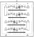
- FIG. 2 is a schematic view showing the first embodiment of the power supply IC 100.
- the power supply IC 100 of this embodiment is a multi-chip type semiconductor device (so-called composite isolator) formed by sealing the primary side control chip 110, the secondary side control chip 120, and the isolator chip 130 in a single package. It is.
- the primary side control chip 110 has an RS flip flop 111 and pads T11 and T12 as a receiving unit for receiving the pulse signals S10 and S20 from the secondary side control chip 120 via the isolator chip 130.
- the primary side control chip 110 also has pulse signal generation units 112 and 113 and pads T13 and T14 as transmitting units that transmit the pulse signals S30 and S40 to the secondary side control chip 120 via the isolator chip 130.
- the reference potential end of the primary side control chip 110 is connected to the ground end GND1.
- the secondary side control chip 120 has pulse signal generation units 121 and 122 and pads T21 and T22 as transmission units that transmit the pulse signals S10 and S20 to the primary side control chip 110 via the isolator chip 130.
- the secondary side control chip 120 also has an RS flip flop 123 and pads T23 and T24 as a receiving unit for receiving the pulse signals S30 and S40 from the primary side control chip 110 via the isolator chip 130.
- the reference potential end of the secondary side control chip 120 is connected to the ground end GND2.
- a one-shot pulse generation circuit can be suitably used.
- the isolator chip 130 electrically insulates between the primary side control chip 110 and the secondary side control chip 120 and, as a means for transmitting pulse signals S10 to S40 between the two chips, an integrated transformer 131 to 134, pads T31a to T34a, and pads T31b to T34b.
- the integration transformers 131 to 134 each include an input winding (solid line) and an output winding (broken line) magnetically coupled to each other with the same polarity.
- the secondary side control chip 120 corresponds to the first chip on the transmission side of the pulse signals S10 and S20
- the primary side control chip 110 corresponds to the pulse signals S10 and S20. It corresponds to the second chip on the receiving side.
- the isolator chip 130 electrically insulates between the primary side control chip 110 and the secondary side control chip 120 using the integration transformers 131 and 132 while the secondary side control chip 120 is connected to the primary side control chip. It corresponds to a third chip for transmitting the pulse signals S10 and S20 to 110.
- the primary side control chip 110 corresponds to the first chip on the transmission side of the pulse signals S30 and S40
- the secondary side control chip 120 corresponds to the pulse signals S30 and S40. It corresponds to the second chip on the receiving side.
- the isolator chip 130 electrically insulates between the primary side control chip 110 and the secondary side control chip 120 using the integration transformers 133 and 134, while the primary side control chip 110 to the secondary side control chip
- the third chip 120 transmits the pulse signals S30 and S40 to the second chip 120.
- the output terminals of the pulse signal generators 121 and 122 are connected to the pads T21 and T22, respectively.
- the pads T21 and T22 are connected to the pads T31 b and T32 b via bonding wires W21 and W22, respectively.
- the pads T31b and T32b are connected to the input windings (solid lines) of the integration transformers 131 and 132, respectively.
- the output windings (broken lines) of the integration transformers 131 and 132 are connected to the pads T31a and T32a.
- the pads T31a and T32a are connected to the pads T11 and T12 via bonding wires W11 and W12, respectively.
- the pads T11 and T12 are connected to the set end (S) and the reset end (R) of the RS flip flop 111, respectively.
- the pulse signal generation unit 122 pulse drives the input winding (solid line) of the integration transformer 132. .
- the RS flip flop 111 sets the output end (Q) to the first logic level (for example, high level) according to the pulse signal S10 input to the set end (S), and is input to the reset end (R) In response to the pulse signal S20, the output terminal (Q) is reset to a second logic level (for example, low level).
- the secondary side control chip 120 is configured to have, for example, an output feedback control unit (not shown) that performs duty control of the pulse width modulation signal PWM such that the divided voltage Vdiv matches the reference voltage Vref.
- the generating units 121 and 122 may be configured to pulse drive the input windings (solid lines) of the integration transformers 131 and 132, for example, at the rising timing and the falling timing of the pulse width modulation signal PWM.
- the primary side control chip 110 may be configured to switch the logic level of the gate signal G1 according to the logic level of the output terminal (Q) of the RS flip flop 111, for example.
- the output terminals of the pulse signal generators 112 and 113 are connected to the pads T13 and T14, respectively.
- Pads T13 and T14 are connected to pads T33a and T34a via bonding wires W13 and W14, respectively.
- Pads T33a and T34a are connected to respective input windings (solid lines) of integration transformers 133 and 134, respectively.
- the output windings (broken lines) of the integration transformers 133 and 134 are connected to the pads T33 b and T34 b.
- the pads T33 b and T34 b are connected to the pads T23 and T24 via bonding wires W23 and W24, respectively.
- the pads T23 and T24 are connected to the set end (S) and the reset end (R) of the RS flip flop 123, respectively.
- the pulse signal generator 113 pulse drives the input winding (solid line) of the integration transformer 134 when resetting the output terminal (Q) of the RS flip flop 123 to the second logic level (for example, low level). .
- the RS flip flop 123 sets the output end (Q) to the first logic level (for example, high level) according to the pulse signal S30 input to the set end (S), and is input to the reset end (R) In response to the pulse signal S40, the output terminal (Q) is reset to the second logic level (for example, low level).
- the primary side control chip 110 is configured to have, for example, an abnormality notification unit (not shown) that generates an abnormality notification signal ERR to the secondary side control chip 120, and the pulse signal generation units 112 and 113 are, for example, abnormality
- Each input winding (solid line) of the integration transformers 133 and 134 may be pulse-driven at the rising timing and the falling timing of the notification signal ERR.
- the secondary side control chip 120 may be configured to switch whether or not to shut down the operation of generating the DC output voltage Vo according to, for example, the logic level of the output terminal (Q) of the RS flip flop 123 .
- the inductor L for forming the LC low pass filter the inductance components of the bonding wires (W21, W22, W13, W14) are actively used.
- the capacitor C for forming the LC low pass filter is formed using the signal input pad (T31b, T32b, T33a, T34a) of the isolation chip 130 and the conductor layer and the dielectric layer in the lower region thereof. (See the hatching area in the figure, details will be described later).
- the pulse signal generation units 121 and 122 and the pulse signal generation units 112 and 113 each have a function of arbitrarily adjusting the pulse width of the pulse signals S10 to S40.
- the noises of the pulse signals S10 to S40 can be appropriately reduced.
- FIG. 3 is an equivalent circuit diagram of the signal transmission path in the first embodiment.
- integrated transformer 210 includes an input winding 211 and an output winding 212 magnetically coupled to each other in the same polarity.
- the LC low pass filter 220 includes an inductor 221 and a capacitor 222.
- the first end of the inductor 221 is connected to the signal input end IN.
- the second end of the inductor 221 and the first end of the capacitor 222 are connected to the first end of the input winding 211 as the output end of the LC low pass filter 220.
- the second end of the capacitor 222 and the second end of the input winding 211 are both connected to the first ground end.
- the first end of the output winding 212 is connected to the signal output end OUT.
- the second end of the output winding 212 is connected to the second ground end.
- the integration transformer 210 is understood as the above-described integration transformer 133 or 134
- the signal input end IN corresponds to the pad T13 or T14
- the capacitor 222 corresponds to the capacitor C formed in the lower region of the pad T33a or T34a
- the signal output end OUT corresponds to the pad T33b or T34b
- the first ground end corresponds to the ground end GND1
- the second ground terminal corresponds to the ground terminal GND2.
- FIG. 4 is a schematic view showing a second embodiment of the power supply IC 100.
- the inductance components of the bonding wires W11, W12, W23, W24
- W11, W12, W23, W24 are actively used as the inductor L for forming the LC low pass filter.
- the capacitor C for forming the LC low pass filter includes the signal input pads (T11, T12, T23, T24) of the primary side control chip 110 and the secondary side control chip 120, and the conductor layer and dielectric in the lower region thereof. It is formed using a body layer (see hatching area in the figure, details will be described later).
- the pulse signal generation units 121 and 122 and the pulse signal generation units 112 and 113 have a function of arbitrarily adjusting the pulse widths of the pulse signals S10 to S40 as in the first embodiment (FIG. 2) described above. It is desirable to have However, when adjusting the pulse width, it is necessary to consider not only the cutoff frequency fc of the LC low pass filter but also the coupling degree of each of the integrated transformers 131 to 134, unlike the first embodiment (FIG. 2) described above. It should be noted that there is a point.
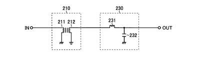
- FIG. 5 is an equivalent circuit diagram of a signal transmission path in the second embodiment.
- the LC low pass filter 230 includes an inductor 231 and a capacitor 232.
- the first end of the input winding 211 is connected to the signal input end IN.
- the second end of the input winding 211 is connected to the first ground end.
- the first end of the output winding 212 is connected to the first end of the inductor 231.
- the second end of the output winding 212 is connected to the second ground end.
- the second end of the inductor 231 and the first end of the capacitor 232 are connected as the output end of the LC low pass filter 230 to the signal output end OUT.
- the second end of the capacitor 232 is connected to the second ground end.
- the second ground terminal corresponds to the ground terminal GND2.
- the first embodiment in which the LC low pass filter 220 is introduced upstream of the integration transformer 210 and the second embodiment (in which the LC low pass filter 230 is introduced downstream of the integration transformer 210) Although FIG. 5) is described separately, the first embodiment and the second embodiment may be combined and adopted. That is, it is also possible to introduce the LC low pass filters 220 and 230 on both the upstream and downstream sides of the integration transformer 210, respectively.
- FIG. 6 is a schematic view showing a first structural example of the capacitor C, in which a longitudinal sectional view (upper stage) and a partial top view (lower stage) of a chip on which the capacitor C is formed are depicted.
- a longitudinal sectional view (upper stage) and a partial top view (lower stage) of a chip on which the capacitor C is formed are depicted.
- a cross section when the chip is cut vertically along line A1-A2 of the partial top view (lower part) is depicted.
- the chip corresponds to the isolator chip 130 of the first embodiment (FIG. 2) or the primary side control chip 110 or the secondary side control chip 120 of the second embodiment (FIG. 4).
- a bonding wire 301 serving as a transmission path of a pulse signal is connected to the pad 302.
- the bonding wire W21 or W22 or the bonding wire W13 or W14 in FIG. 2 corresponds to the bonding wire 301 in FIG. 2, and the pad T31b or T32b or the pad T33a in FIG.
- T34a corresponds to the pad 302 in this figure.
- the bonding wire W11 or W12 or the bonding wire W23 or W24 in FIG. 4 corresponds to the bonding wire 301 in this figure
- T24 corresponds to the pad 302 in this figure.
- the chip in this figure has a two-layer wiring structure in which a first metal layer (1st MTL), an interlayer insulating layer (ILD), and a second metal layer (2nd MTL) are sequentially formed from the lower layer side (substrate side). It is assumed.
- a first metal layer (1st MTL), an interlayer insulating layer (ILD), and a second metal layer (2nd MTL) are sequentially formed from the lower layer side (substrate side).
- Al, Cu, etc. can be mentioned as a raw material of each metal layer (1stMTL, 2ndMTL).
- SiO 2 etc. can be mentioned as a raw material of an interlayer insulation layer (ILD).
- Metal wires 303 and 306 are laid in the second metal layer (2nd MTL) described above.
- a rectangular (for example, 100 ⁇ m ⁇ 100 ⁇ m) pad connection region is formed in the plan view, and an electrical connection with the pad 302 is established in the region. That is, the pad connection region of the metal wire 303 functions as a first electrode for receiving an input of a pulse signal from the chip of the previous stage through the bonding wire 301 and the pad 302. Therefore, in the following description, the pad connection region of the metal wire 303 may be referred to as the first electrode 303 in some cases.
- a pad connection region similar to the above is formed also in the metal wiring 306, and electrical connection with the pad 307 is established in the region.
- the metal wiring 306 is connected to the metal wiring 304 laid in the first metal layer (1st MTL) through the via 305 which penetrates the interlayer insulating layer (ILD).
- electrical insulation is maintained between the rectangular region and the first electrode 303 by separating an interlayer insulating layer (ILD). That is, the rectangular region functions as a second electrode electrically isolated from the first electrode 303 and connected to the reference potential end. Therefore, in the following description, the rectangular region of the metal wire 304 may be referred to as a second electrode 304.
- the capacitor C can be formed by the first electrode 303 and the second electrode 304 which are conductors, and the dielectric (interlayer insulating layer (ILD)) sandwiched between both electrodes. it can. Further, in the present structural example, since the lower region of the pad 302 can be effectively used, the area of the chip is not unnecessarily increased when forming the capacitor C.
- ILD interlayer insulating layer
- FIG. 7 is a schematic view showing a second structure example of the capacitor C.
- a polysilicon layer (poly-Si) is formed on the lower layer side (substrate side) of the first metal layer (1st MTL) based on the first structure example (FIG. 6) described above. It has a three-layer wiring structure.
- metal wires 303 and 306 are laid in the second metal layer (2nd MTL) described above.
- the rectangular pad connection region formed in the metal wiring 303 functions as the first electrode described above, which is the same as the above.
- the metal wiring layer 306 is connected to the metal wiring 315 laid in the first metal layer (1st MTL) via the via 316 penetrating the second interlayer insulating layer (2nd ILD). Furthermore, the metal wire 315 is connected to the polysilicon wire 313 laid in the polysilicon layer (poly-Si) via the via 314 penetrating the first interlayer insulating layer (1st ILD).
- the polysilicon wiring 313 is extended to the lower region of the first electrode 303, and a rectangular region having the same area as the first electrode 303 is formed in the plan view.
- the rectangular area functions as the aforementioned second electrode. Therefore, in the following description, the rectangular region of the polysilicon wiring 313 may be referred to as a second electrode 313.
- the distance between the first electrode 303 and the second electrode 313 in FIG. 7 is longer than the distance between the first electrode 303 and the second electrode 304 in FIG.
- the capacitance value of the capacitor C is reduced.
- an intermediate electrode 312 formed using a first metal layer (1st MTL) is additionally provided between the first electrode 303 and the second electrode 313.
- the intermediate electrode 312 is short-circuited with the first electrode 303 through the via 311 penetrating the second interlayer insulating layer (2nd ILD).
- electrical insulation is maintained by separating the first interlayer insulating layer (1st ILD).
- the capacitor C is formed by the intermediate electrode 312 and the second electrode 313 which are conductors, and the dielectric (first interlayer insulating layer (1st ILD)) sandwiched between both electrodes. Can. Therefore, even when the distance between the first electrode 303 and the second electrode 313 is extended with the multilayer wiring of the chip, the capacitance value of the capacitor C can be maintained.
- the intermediate electrode 312 may be formed in a rectangular shape having an area equal to or larger than that of the first electrode 303 and the second electrode 313 in plan view.
- the intermediate electrode 312 and the first electrode 303 are short-circuited to insulate the intermediate electrode 312 and the second electrode 313 by way of example.
- the first electrode 303 may be insulated and the middle electrode 312 and the second electrode 313 may be short-circuited.
- the capacitor C is formed by the first electrode 303 and the intermediate electrode 312 which are conductors, and the dielectric (second interlayer insulating layer (2nd ILD)) sandwiched between both electrodes.
- FIG. 8 is a schematic view showing a third structure example of the capacitor C.
- the second electrode 401 polysilicon layer
- the first intermediate electrode 402 first metal layer
- the second intermediate electrode 403 second metal layer
- the first electrode 404 third metal layer
- the first intermediate electrode 402 is short-circuited with the first electrode 404.
- the second intermediate electrode 403 is short-circuited with the second electrode 401.
- first intermediate electrode 402 shorted to the first electrode 401 and at least one shorted to the second electrode 401 are used as the above-described intermediate electrodes.
- Layers of second intermediate electrodes 403 are alternately stacked.
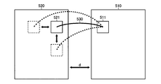
- the first chip 510 on the transmission side of the pulse signal is provided with a pad 511 for outputting the pulse signal.
- the second chip 520 on the receiving side of the pulse signal is provided with a pad 521 for receiving an input of the pulse signal.
- the bonding wire 530 is connected between the pad 511 and the pad 521.
- the length l, the diameter ⁇ , the number n, or the material of the bonding wire 530 it is conceivable to adjust the length l, the diameter ⁇ , the number n, or the material of the bonding wire 530.
- the distance d between both chips may be changed, or the position of the pad 511 or the pad 521 may be changed.
- FIG. 10 is a schematic diagram for specifically explaining the adjustment method of the inductance value.
- FIG. 10 an example is given in which the positions of the pads T32a and T32b are changed based on FIG. 4 described above.
- bonding wires W12 and W22 connected to pads T32a and T32b, respectively can be made longer than other bonding wires to increase their inductance values.
- the length l of the bonding wire (and hence the inductance value of the inductor L forming the LC low pass filter) can be arbitrarily adjusted by the position of the pad.
- the inductance value of the inductor L forming the LC low-pass filter varies not only with the length l of the bonding wire, but also with the diameter ⁇ , the number n, or the material. Therefore, in order to optimize the cutoff frequency of the LC low pass filter, it is necessary to adjust the capacitance value of the capacitor C in accordance with the inductance value of the inductor L.
- a method of adjusting the capacitance value of the capacitor C will be described in detail by giving a specific example.
- FIG. 11 is a schematic view showing a fourth structural example of the capacitor C, in which a longitudinal sectional view of a chip in which the capacitor C is formed is depicted.
- the chip corresponds to the isolator chip 130 of the first embodiment (FIG. 2).
- the chip of this structural example has a five-layer wiring structure in which a polysilicon layer 600 and metal layers 610 to 640 are sequentially stacked from the lower layer side (substrate side).
- an interlayer insulating layer 650 is formed between the polysilicon layer 600 and the metal layer 610.
- interlayer insulating layers 660 to 680 are formed between the metal layers 610 to 640, respectively.
- the polysilicon layer 600, the interlayer insulating layer 650, the metal layer 610, the interlayer insulating layer 660, the metal layer 620, the interlayer insulating layer 670, the metal layer 630, and the layers are sequentially from the lower layer side (substrate side).
- the insulating layer 680 and the metal layer 640 are stacked.
- Examples of the material of the metal layers 610 to 640 include Al and Cu.
- a polysilicon wiring 601 is laid.
- Metal wires 611 and 612 are laid in the metal layer 610.
- Metal interconnection 612 is connected to polysilicon interconnection 601 through via 651 penetrating interlayer insulating layer 650.
- metal wires 621 to 623 are laid.
- the metal wire 621 is connected to the metal wire 611 through a via 661 penetrating the interlayer insulating layer 660.
- electrical insulation is maintained between the polysilicon wiring 601 and the metal wiring 621 with the interlayer insulating layers 650 and 660 separated.
- Metal interconnections 622 and 623 are connected to metal interconnection 612 through vias 662 and 663 penetrating interlayer insulating layer 660, respectively.
- metal wires 631 and 632 are laid.
- Metal interconnection 631 is connected to metal interconnections 621 and 622 through vias 671 and 672 penetrating interlayer insulating layer 670.
- Metal interconnection 632 is connected to metal interconnection 623 through via 673 penetrating interlayer insulating layer 670.
- the input winding of the integration transformer is formed by the conductive path (metal wiring 631 ⁇ via 672 ⁇ metal wiring 622 ⁇ via 662 ⁇ metal wiring 612) laid in the central portion of this figure.
- metal wires 641 and 642 are laid.
- Metal interconnection 641 is connected to metal interconnection 631 through via 681 penetrating interlayer insulating layer 680.
- the metal wire 641 is formed in a rectangular shape in a plan view, and functions as a pad for receiving an input of a pulse signal through a bonding wire. That is, the metal wiring 641 corresponds to the pad T31b or T32b or the pad T33a or T34a in the first embodiment (FIG. 2).
- metal interconnection 642 is connected to metal interconnection 632 through via 682 penetrating through interlayer insulating layer 680.
- an insulating layer 691 is formed so as to fill the peripheries of the metal wires 641 and 642. Furthermore, on the outermost surface of the chip, a protective layer 692 is formed which protects the surface of the chip while exposing at least a part of the metal wires 641 and 642 functioning as pads.
- a material of the protective layer 692 polyimide and the like can be mentioned.
- capacitor C having metal interconnections 611 and 621 as the first electrode, polysilicon interconnection 601 as the second electrode, and interlayer insulating layers 650 and 660 sandwiched between both electrodes as the dielectric. Can be formed.
- the bonding wire connected to the pad functions as the inductor L forming the LC low pass filter, and the metal wire 641 functioning as the pad (further connected to this)
- the metal wires 611 and 621 function as a first electrode of the capacitor C which forms an LC low pass filter.
- the facing area S can be adjusted by the area and the number of the metal wires 611 and 621 facing the polysilicon wire 601.
- the inter-electrode distance d can be adjusted depending on which wiring layer is used as the first electrode and the second electrode of the capacitor C among the plurality of stacked wiring layers. More specifically, in the chip of this structural example, both of the metal wires 611 and 621 are used as the first electrode of the capacitor C. For example, the metal wire 611 is omitted and only the metal wire 621 is used as the capacitor C. When the first electrode is used, the inter-electrode distance d can be extended to reduce the capacitance value of the capacitor C. The inter-electrode distance d can also be adjusted arbitrarily by optimizing the thickness itself of the interlayer insulating layer by changing the manufacturing process of the chip.
- the characteristics (capacitance value and equivalent series resistance value) of the capacitor C can be easily adjusted as the number of wiring stages (the number of stacked layers) of the chip increases and the interlayer insulating layer becomes thinner.
- FIG. 12 is a schematic view showing a fifth structure example of the capacitor C.
- a longitudinal sectional view (upper stage), a partial plan view (middle stage), and a partially enlarged view (lower stage) of a chip on which the capacitor C is formed. Is depicted.
- a cross section when the chip is cut vertically along line A3-A4 of the partial plan view (middle stage) is depicted.
- the partial plan view (middle) metal wires 711 and 712 in perspective from the chip surface are depicted.
- the partial enlarged view (lower part) the inside of the round frame of the partial plan view (middle part) is depicted in a partially enlarged manner.
- the chip of this structural example has a three-layer wiring structure in which a polysilicon layer 700 and metal layers 710 and 720 are laminated in order from the lower layer side (substrate side).
- an interlayer insulating layer 730 is formed between the polysilicon layer 700 and the metal layer 710.
- an interlayer insulating layer 740 is formed between the metal layer 710 and the metal layer 720.
- the polysilicon layer 700, the interlayer insulating layer 730, the metal layer 710, the interlayer insulating layer 740, and the metal layer 720 are sequentially formed in order from the lower layer side (substrate side).
- the depiction of the insulating layer and the protective layer covering the chip surface is omitted.
- a polysilicon wiring 701 is laid.
- metal wires 711 to 713 are laid.
- Metal interconnections 711 and 713 are connected to polysilicon interconnection 701 via vias 731 and 732 penetrating interlayer insulating layer 730, respectively.
- electrical insulation is maintained between the polysilicon wiring 701 and the metal wiring 721 with the interlayer insulating layer 730 therebetween.
- the metal wires 711 and 712 have features in their respective planar shapes, which will be described in detail later.
- metal wires 721 and 722 are laid.
- the metal wire 721 is connected to the metal wire 712 through a via 741 penetrating the interlayer insulating layer 740.
- the metal wire 721 is formed in a rectangular shape in a plan view, and functions as a pad for receiving an input of a pulse signal through a bonding wire.
- metal interconnection 722 is connected to metal interconnection 713 through via 742 penetrating interlayer insulating layer 740.
- metal interconnection 712 is used as the first electrode
- polysilicon interconnection 701 and metal interconnection 711 as the second electrode
- interlayer insulating layers 730 and 740 sandwiched between both electrodes are used as dielectrics.
- Capacitor C can be formed.
- comb teeth 711a and 711b which intermesh with each other at a predetermined inter-electrode distance (a so-called MIM [Metal-Insulator-Metal] structure).
- MIM Metal-Insulator-Metal
- FIG. 13 is a schematic view showing a fifth structure example of the capacitor C.
- a longitudinal sectional view (upper stage) and a top view (lower stage) of a chip in which the capacitor C is formed are depicted.
- a vertical cross-sectional view (upper stage) a cross section when the chip is cut vertically along line A5-A6 in the top view (lower stage) is depicted.
- the introduction target of the LC low pass filter is not limited to various chips handling the pulse signal inside the power supply IC 100 (the primary side control chip 110, the secondary side control chip 120, and the isolator chip 130). It can be extended to understand in general the chip to which the pulse signal is input through the wire.
- the semiconductor device disclosed in the present specification can be used for, for example, in-vehicle devices and industrial devices.
- Isolated switching power supply 1p Primary circuit system (GND1 system) 1s Secondary circuit system (GND2 system) 2 load 10 rectification unit 11 filter 12 diode bridge 13, 14 capacitor 20 DC / DC conversion unit 100 power supply IC DESCRIPTION OF SYMBOLS 110 Primary side control chip 111 RS flip flop 112, 113 Pulse signal generation part 120 Secondary side control chip 121, 122 Pulse signal generation part 123 RS flip flop 130 Isolator chip 131-134 Integration transformer 210 Integration transformer 211 Input winding 212 output winding 220, 230 LC low pass filter 221, 231 inductor 222, 232 capacitor 301 bonding wire 302, 307 pad 303 metal wiring (first electrode) 304 Metal wiring (second electrode) 312 middle electrode 313 polysilicon wiring (second electrode) 306, 315 Metal wiring 305, 311, 314, 316 Via 401 Second electrode 402 First intermediate electrode 403 Second intermediate electrode 404 First electrode 510 First chip 511 Pad 520 Second chip 521 Pad 530 Bonding
Landscapes
- Engineering & Computer Science (AREA)
- Power Engineering (AREA)
- Computer Networks & Wireless Communication (AREA)
- Signal Processing (AREA)
- Semiconductor Integrated Circuits (AREA)
- Dc-Dc Converters (AREA)
- Dc Digital Transmission (AREA)
Abstract
半導体装置は、パルス信号の送信側となる第1チップと、パルス信号の受信側となる第2チップと、集積化トランスを用いて第1チップと第2チップとの間を電気的に絶縁しつつ第1チップから第2チップにパルス信号を伝送する第3チップとを有する。第2チップと第3チップは、それぞれ、前段のボンディングワイヤを介してパルス信号の入力を受け付けるための第1電極を備えている。各チップの第1電極のうち、少なくとも一方の下方領域には、第1電極と電気的に絶縁されるとともに基準電位端に接続された第2電極が設けられている。これにより、LCローパスフィルタを形成することができるので、パルス信号のノイズを削減することが可能となる。
Description
本明細書中に開示されている発明は、パルス信号を取り扱う半導体装置(例えば複合化アイソレータ)に関する。
従来より、例えば、車載機器や産業機器の電源として用いられるAC/DCコンバータやDC/DCコンバータの分野では、アイソレータを用いて1次回路系と2次回路系を磁気結合しながら両者の絶縁性を保つ技術が存在する。
なお、上記に関連する従来技術の一例としては、特許文献1を挙げることができる。
しかしながら、アイソレータの周囲に多くのスイッチングノイズが発生する環境では、正確にパルス信号を伝送することが難しく、特に、入力電圧の高いAC/DCコンバータでは、アイソレータに生じるノイズレベルが大きいという課題があった。
なお、上記の課題は、アイソレータだけでなく、パルス信号を取り扱う半導体装置全般に当てはまる。
本明細書中に開示されている発明は、本願の発明者が見出した上記の課題に鑑み、パルス信号のノイズを削減することのできる半導体装置を提供することを目的とする。
本明細書中に開示されている半導体装置は、パルス信号の送信側となる第1チップと、前記パルス信号の受信側となる第2チップと、集積化トランスを用いて前記第1チップと前記第2チップとの間を電気的に絶縁しつつ前記第1チップから前記第2チップに前記パルス信号を伝送する第3チップを有し、前記第2チップと前記第3チップは、それぞれ、前段のチップからボンディングワイヤを介して前記パルス信号の入力を受け付けるための第1電極を備えており、各チップの第1電極のうち、少なくとも一方の下方領域には、前記第1電極と電気的に絶縁されるとともに基準電位端に接続された第2電極が設けられている構成(第1の構成)とされている。
なお、第1の構成から成る半導体装置において、前記第2電極は、メタル層またはポリシリコン層を用いて形成されている構成(第2の構成)にするとよい。
また、第1または第2の構成から成る半導体装置において、前記第2電極は、その平面視において、前記第1電極と同一以上の面積を持つ構成(第3の構成)にするとよい。
また、第1~第3いずれかの構成から成る半導体装置において、前記第1電極と前記第2電極との間には、前記第1電極及び前記第2電極の一方に短絡された少なくとも一層の中間電極が設けられている構成(第4の構成)にするとよい。
また、第4の構成から成る半導体装置において、前記第1電極と前記第2電極との間には、前記中間電極として、前記第1電極に短絡された少なくとも一層の第1中間電極と、前記第2電極に短絡された少なくとも一層の第2中間電極とが交互に積層されている構成(第5の構成)にするとよい。
また、第1~第5いずれかの構成から成る半導体装置において、前記第1チップは、前記パルス信号のパルス幅を調整する機能を備えた構成(第6の構成)にするとよい。
また、第1~第6いずれかの構成から成る半導体装置は、一次回路系と二次回路系を電気的に絶縁しつつ相互間の信号伝送を行うことにより絶縁型スイッチング電源の制御主体として機能する構成(第7の構成)にするとよい。
また、本明細書中に開示されている絶縁型スイッチング電源は、第7の構成から成る半導体装置と、前記半導体装置により制御されるスイッチング出力段と、を有する構成(第8の構成)とされている。
なお、第8の構成から成る絶縁型スイッチング電源において、前記スイッチング出力段は、トランスを用いて一次回路系と二次回路系を電気的に絶縁しつつ、前記一次回路系に供給される直流入力電圧から直流出力電圧を生成して前記二次回路系の負荷に供給するDC/DC変換部の構成要素として機能する構成(第9の構成)にするとよい。
また、第9の構成から成る絶縁型スイッチング電源は、交流入力電圧から前記直流入力電圧を生成する整流部をさらに有する構成(第10の構成)にするとよい。
また、本明細書中に開示されている電子機器は、第8~第10いずれかの構成から成る絶縁型スイッチング電源と、前記絶縁型スイッチング電源から電力供給を受けて動作する負荷と、を有する構成(第11の構成)とされている。
また、本明細書中に開示されているチップは、ボンディングワイヤを介してパルス信号の入力を受け付けるための第1電極と、前記第1電極の下方領域に設けられて前記第1電極と電気的に絶縁されるとともに基準電位端に接続された第2電極と、を集積化して成る構成(第12の構成)とされている。
また、本明細書中に開示されているチップは、ワイヤを介してパルス信号の入力を受け付けるためのパッドを有し、前記ワイヤがフィルタを形成するインダクタとして機能し、前記パッドまたはこれに接続された配線層が前記フィルタを形成するキャパシタの第1電極として機能する構成(第13の構成)とされている。
なお、第13の構成から成るチップにおいて、前記インダクタのインダクタンス値は、前記ワイヤの長さ、直径、本数、または、素材により調整される構成(第14の構成)にするとよい。
また、第14の構成から成るチップにおいて、前記ワイヤの長さは、前記パッドの位置により調整される構成(第15の構成)にするとよい。
また、第13~第15いずれかの構成から成るチップにおいて、前記キャパシタの容量値は、前記第1電極と第2電極との対向面積又は電極間距離により調整される構成(第16の構成)にするとよい。
また、第16の構成から成るチップにおいて、前記第1電極と前記第2電極との電極間距離は、積層形成された複数の配線層のうち、前記第1電極及び前記第2電極としていずれの配線層を用いるかにより調整される構成(第17の構成)にするとよい。
また、第17の構成から成るチップにおいて、前記第1電極と前記第2電極との電極間距離は、層間絶縁層の厚さにより調整される構成(第18の構成)にするとよい。
また、第16の構成から成るチップにおいて、前記第1電極と前記第2電極は、同一の配線層に形成されており、前記電極間距離を隔てて相互に噛み合う櫛歯を備えている構成(第19の構成)にするとよい。
また、第13~第19いずれかの構成から成るチップは、前記パッドを露出しつつ前記チップの表面を被覆する保護層をさらに有する構成(第20の構成)にするとよい。
本明細書中に開示されている発明によれば、パルス信号のノイズを削減することのできる半導体装置を提供することが可能となる。
<絶縁型スイッチング電源>
図1は、絶縁型スイッチング電源を備えた電子機器の全体構成を示したブロック図である。本構成例の電子機器Xは、絶縁型スイッチング電源1と、絶縁型スイッチング電源1から電力供給を受けて動作する負荷2と、を有する。
図1は、絶縁型スイッチング電源を備えた電子機器の全体構成を示したブロック図である。本構成例の電子機器Xは、絶縁型スイッチング電源1と、絶縁型スイッチング電源1から電力供給を受けて動作する負荷2と、を有する。
絶縁型スイッチング電源1は、一次回路系1p(GND1系)と二次回路系1s(GND2系)との間を電気的に絶縁しつつ、商用交流電源PWから一次回路系1pに供給される交流入力電圧Vac(例えばAC85~265V)を所望の直流出力電圧Vo(例えばDC10~30V)に変換して、二次回路系1sの負荷2に供給するAC/DCコンバータであり、整流部10と、DC/DC変換部20と、を含む。
整流部10は、交流入力電圧Vacから直流入力電圧Vi(例えばDC120~375V)を生成してDC/DC変換部20に供給する回路ブロックであり、フィルタ11と、ダイオードブリッジ12と、キャパシタ13及び14とを含む。フィルタ11は、交流入力電圧Vacからノイズやサージを除去する。ダイオードブリッジ12は、交流入力電圧Vacを全波整流して直流入力電圧Viを生成する。キャパシタ13は、交流入力電圧Vacの高調波ノイズを除去する。キャパシタ14は、直流入力電圧Viを平滑化する。なお、整流部10の前段には、フューズなどの保護素子を設けてもよい。
DC/DC変換部20は、直流入力電圧Viから所望の直流出力電圧Voを生成して負荷2に供給する回路ブロックであり、電源IC100と、これに外付けされる種々のディスクリート部品(トランスTR、Nチャネル型MOS電界効果トランジスタN1、センス抵抗Rs、ダイオードD1、キャパシタC1、並びに、抵抗R1及びR2)と、を含む。
電源IC100は、アイソレータチップ130(詳細は後述)を用いて一次回路系1pと二次回路系1sとの間を電気的に絶縁しつつ、相互間の信号伝送を行うことにより、絶縁型スイッチング電源1(特にDC/DC変換部20)の制御主体として機能する半導体装置である。例えば、電源IC100は、二次回路系1sで生成される分圧電圧Vdiv(=直流出力電圧Voの分圧電圧)の帰還入力を受け付けて、一次回路系1pに設けられたトランジスタN1のオン/オフ制御を行う。
トランスTRは、一次回路系1pと二次回路系1sとの間を電気的に絶縁しつつ互いに逆極性で磁気結合された一次巻線Lp(巻数Np)と二次巻線Ls(巻数Ns)を含む。一次巻線Lpの第1端は、直流入力電圧Viの印加端に接続されている。一次巻線Lpの第2端は、トランジスタN1のドレインに接続されている。二次巻線Lsの第1端は、ダイオードD1のアノードに接続されている。二次巻線Lsの第2端は、二次回路系1sの接地端GND2に接続されている。なお、巻数Np及びNsについては、所望の直流出力電圧Voが得られるように任意に調整すればよい。例えば、巻数Npが多いほど又は巻数Nsが少ないほど直流出力電圧Voは低くなり、逆に、巻数Npが少ないほど又は巻数Nsが多いほど直流出力電圧Voは高くなる。
トランジスタN1は、電源IC100から入力されるゲート信号G1に応じてオン/オフされる出力スイッチ素子として機能する。具体的に述べると、トランジスタN1は、ゲート信号G1がハイレベルであるときにオンし、ゲート信号G1がローレベルであるときにオフする。トランジスタN1のドレインは、先に述べたように、一次巻線Lpの第2端に接続されている。トランジスタN1のソースは、センス抵抗Rsの第1端に接続されている。センス抵抗Rsの第2端は、一次回路系1pの接地端GND1に接続されている。センス抵抗Rsは、トランジスタN1に流れる一次電流Ipをセンス電圧Vs(=Ip×Rs)として検出するための電流/電圧変換素子として機能する。
ダイオードD1のアノードは、先に述べたように、二次巻線Lsの第1端に接続されている。ダイオードD1のカソードとキャパシタC1の第1端は、いずれも直流出力電圧Voの出力端に接続されている。キャパシタC1の第2端は、接地端GND2に接続されている。このように接続されたダイオードD1とキャパシタC1は、二次巻線Lsに生じる誘起電圧を整流及び平滑して直流出力電圧Voを生成する整流平滑部として機能する。
抵抗R1及びR2は、直流出力電圧Voの出力端と接地端GND2との間に直列接続されており、相互間の接続ノードから分圧電圧Vdiv(=Vo×R2/(R1+R2))を出力する分圧部として機能する。
なお、上記構成から成るDC/DC変換部20において、トランスTR、トランジスタN1、ダイオードD1、及び、キャパシタC1は、フライバック方式により直流入力電圧Viから直流出力電圧Voを生成するスイッチング出力段として機能する。
次に、当該スイッチング出力段の降圧動作について簡単に説明する。トランジスタN1がオンされているときには、直流入力電圧Viの印加端から、一次巻線Lp、トランジスタN1、及び、センス抵抗Rsを介して、接地端GND1に向けた一次電流Ipが流れるので、一次巻線Lpに電気エネルギが蓄えられる。
その後、トランジスタN1がオフされると、一次巻線Lpと磁気結合された二次巻線Lsに誘起電圧が発生し、二次巻線LsからダイオードD1を介して接地端GND2に向けた二次電流Isが流れる。このとき、負荷2には、二次巻線Lsの誘起電圧を整流及び平滑した直流出力電圧Voが供給される。
以降も、トランジスタN1がオン/オフされることにより、上記と同様のスイッチング動作が繰り返される。
このように、本構成例の絶縁型スイッチング電源1によれば、一次回路系1pと二次回路系1sとの間を電気的に絶縁しつつ、交流入力電圧Vacから直流出力電圧Voを生成して負荷2に供給することができる。
<電源IC(第1実施形態)>
図2は、電源IC100の第1実施形態を示す模式図である。本実施形態の電源IC100は、一次側制御チップ110と、二次側制御チップ120と、アイソレータチップ130とを単一のパッケージに封止して成るマルチチップ型の半導体装置(いわゆる複合化アイソレータ)である。
図2は、電源IC100の第1実施形態を示す模式図である。本実施形態の電源IC100は、一次側制御チップ110と、二次側制御チップ120と、アイソレータチップ130とを単一のパッケージに封止して成るマルチチップ型の半導体装置(いわゆる複合化アイソレータ)である。
一次側制御チップ110は、二次側制御チップ120からアイソレータチップ130を介してパルス信号S10及びS20を受信する受信部として、RSフリップフロップ111とパッドT11及びT12を有する。また、一次側制御チップ110は、アイソレータチップ130を介して二次側制御チップ120にパルス信号S30及びS40を送信する送信部として、パルス信号生成部112及び113とパッドT13及びT14を有する。なお、一次側制御チップ110の基準電位端は、接地端GND1に接続されている。
二次側制御チップ120は、アイソレータチップ130を介して一次側制御チップ110にパルス信号S10及びS20を送信する送信部として、パルス信号生成部121及び122とパッドT21及びT22を有する。また、二次側制御チップ120は、一次側制御チップ110からアイソレータチップ130を介してパルス信号S30及びS40を受信する受信部として、RSフリップフロップ123とパッドT23及びT24を有する。なお、二次側制御チップ120の基準電位端は、接地端GND2に接続されている。
なお、上記のパルス信号生成部112及び113、並びに、パルス信号生成部121及び122としては、例えば、1ショットパルス生成回路を好適に用いることができる。
アイソレータチップ130は、一次側制御チップ110と二次側制御チップ120との間を電気的に絶縁しつつ、両チップ間でパルス信号S10~S40を伝送するための手段として、集積化トランス131~134と、パッドT31a~T34aと、パッドT31b~T34bと、を有する。なお、集積化トランス131~134は、それぞれ、互いに同極性で磁気結合された入力巻線(実線)と出力巻線(破線)を含む。
なお、パルス信号S10及びS20に着目した場合には、二次側制御チップ120がパルス信号S10及びS20の送信側となる第1チップに相当し、一次側制御チップ110がパルス信号S10及びS20の受信側となる第2チップに相当する。また、アイソレータチップ130は、集積化トランス131及び132を用いて一次側制御チップ110と二次側制御チップ120との間を電気的に絶縁しつつ、二次側制御チップ120から一次側制御チップ110にパルス信号S10及びS20を伝送する第3チップに相当する。
一方、パルス信号S30及びS40に着目した場合には、一次側制御チップ110がパルス信号S30及びS40の送信側となる第1チップに相当し、二次側制御チップ120がパルス信号S30及びS40の受信側となる第2チップに相当する。また、アイソレータチップ130は、集積化トランス133及び134を用いて一次側制御チップ110と二次側制御チップ120との間を電気的に絶縁しつつ、一次側制御チップ110から二次側制御チップ120にパルス信号S30及びS40を伝送する第3チップに相当する。
次に、パルス信号S10及びS20の伝送経路に着目し、それぞれの上流側から順に、各要素間の接続関係について述べる。パルス信号生成部121及び122の各出力端は、それぞれ、パッドT21及びT22に接続されている。パッドT21及びT22は、それぞれ、ボンディングワイヤW21及びW22を介してパッドT31b及びT32bに接続されている。パッドT31b及びT32bは、それぞれ、集積化トランス131及び132の各入力巻線(実線)に接続されている。集積化トランス131及び132の各出力巻線(破線)は、パッドT31a及びT32aに接続されている。パッドT31a及びT32aは、それぞれ、ボンディングワイヤW11及びW12を介してパッドT11及びT12と接続されている。パッドT11及びT12は、それぞれ、RSフリップフロップ111のセット端(S)及びリセット端(R)に接続されている。
続いて、パルス信号S10及びS20の伝送動作を説明する。パルス信号生成部121は、RSフリップフロップ111の出力端(Q)を第1論理レベル(例えばハイレベル)にセットするときに、集積化トランス131の入力巻線(実線)をパルス駆動する。その結果、集積化トランス131の出力巻線(破線)に誘起パルスが生じ、これがパルス信号S10(=セット信号に相当)として、RSフリップフロップ111のセット端(S)に伝送される。
一方、パルス信号生成部122は、RSフリップフロップ111の出力端(Q)を第2論理レベル(例えばローレベル)にリセットするときに、集積化トランス132の入力巻線(実線)をパルス駆動する。その結果、集積化トランス132の出力巻線(破線)に誘起パルスが生じ、これがパルス信号S20(=リセット信号に相当)として、RSフリップフロップ111のリセット端(R)に伝送される。
RSフリップフロップ111は、セット端(S)に入力されるパルス信号S10に応じて、出力端(Q)を第1論理レベル(例えばハイレベル)にセットし、リセット端(R)に入力されるパルス信号S20に応じて、出力端(Q)を第2論理レベル(例えばローレベル)にリセットする。
なお、二次側制御チップ120は、例えば、分圧電圧Vdivが基準電圧Vrefと一致するようにパルス幅変調信号PWMのデューティ制御を行う出力帰還制御部(不図示)を有する構成とし、パルス信号生成部121及び122は、例えば、パルス幅変調信号PWMの立上りタイミング及び立下りタイミングで、集積化トランス131及び132の各入力巻線(実線)をパルス駆動する構成としておけばよい。また、一次側制御チップ110は、例えば、RSフリップフロップ111の出力端(Q)の論理レベルに応じてゲート信号G1の論理レベルを切り替える構成にしておけばよい。
次に、パルス信号S30及びS40の伝送経路に着目し、それぞれの上流側から順に各要素間の接続関係について述べる。パルス信号生成部112及び113の各出力端は、それぞれ、パッドT13及びT14に接続されている。パッドT13及びT14は、それぞれ、ボンディングワイヤW13及びW14を介してパッドT33a及びT34aに接続されている。パッドT33a及びT34aは、それぞれ、集積化トランス133及び134の各入力巻線(実線)に接続されている。集積化トランス133及び134の各出力巻線(破線)は、パッドT33b及びT34bに接続されている。パッドT33b及びT34bは、それぞれ、ボンディングワイヤW23及びW24を介してパッドT23及びT24と接続されている。パッドT23及びT24は、それぞれ、RSフリップフロップ123のセット端(S)及びリセット端(R)に接続されている。
続いて、パルス信号S30及びS40の伝送動作を説明する。パルス信号生成部112は、RSフリップフロップ123の出力端(Q)を第1論理レベル(例えばハイレベル)にセットするときに、集積化トランス133の入力巻線(実線)をパルス駆動する。その結果、集積化トランス133の出力巻線(破線)に誘起パルスが生じ、これがパルス信号S30(=セット信号に相当)として、RSフリップフロップ123のセット端(S)に伝送される。
一方、パルス信号生成部113は、RSフリップフロップ123の出力端(Q)を第2論理レベル(例えばローレベル)にリセットするときに、集積化トランス134の入力巻線(実線)をパルス駆動する。その結果、集積化トランス134の出力巻線(破線)に誘起パルスが生じ、これがパルス信号S40(=リセット信号に相当)として、RSフリップフロップ123のリセット端(R)に伝送される。
RSフリップフロップ123は、セット端(S)に入力されるパルス信号S30に応じて、出力端(Q)を第1論理レベル(例えばハイレベル)にセットし、リセット端(R)に入力されるパルス信号S40に応じて、出力端(Q)を第2論理レベル(例えばローレベル)にリセットする。
なお、一次側制御チップ110は、例えば、二次側制御チップ120への異常報知信号ERRを生成する異常報知部(不図示)を有する構成とし、パルス信号生成部112及び113は、例えば、異常報知信号ERRの立上りタイミング及び立下りタイミングで、集積化トランス133及び134の各入力巻線(実線)をパルス駆動する構成としておけばよい。また、二次側制御チップ120は、例えば、RSフリップフロップ123の出力端(Q)の論理レベルに応じて、直流出力電圧Voの生成動作をシャットダウンするか否かを切り替える構成にしておけばよい。
ところで、電源IC100のパッケージには、アイソレータチップ130だけでなく、スイッチングノイズを発生する一次側制御チップ110や二次側制御チップ120が封止されている。このように、アイソレータチップ130の周囲に多くのスイッチングノイズが発生する環境では、正確にパルス信号S10~S40を伝送することが難しい。特に、高い交流入力電圧Vacが入力される絶縁型スイッチング電源1では、アイソレータチップ130に生じるノイズレベルが大きいので、これを削減することが非常に重要となる。
そこで、本実施形態の電源IC100では、集積化トランス131~134それぞれの上流側(=入力巻線側)に、LCローパスフィルタが導入されている。特に、LCローパスフィルタを構成するためのインダクタLとしては、ボンディングワイヤ(W21、W22、W13、W14)のインダクタンス成分が積極的に利用されている。また、LCローパスフィルタを構成するためのキャパシタCは、アイソレーションチップ130の信号入力パッド(T31b、T32b、T33a、T34a)とその下方領域における導電体層及び誘電体層を利用して形成されている(図中のハッチング領域を参照、詳細は後述)。
このように、集積化トランス131~134それぞれの上流側に、LCローパスフィルタ220を導入することにより、アイソレータチップ130を介して伝送されるパルス信号S10~S40それぞれのノイズを効果的に削減することが可能となる。
なお、パルス信号生成部121及び122、並びに、パルス信号生成部112及び113は、それぞれ、パルス信号S10~S40のパルス幅を任意に調整する機能を備えている。当該機能を具備することにより、LCローパスフィルタのカットオフ周波数fc(=1/(2π・√(LC))が多少ばらついても、パルス信号S10~S40のパルス幅を最適化することができるので、パルス信号S10~S40のノイズを適切に削減することが可能となる。
図3は、第1実施形態における信号伝送経路の等価回路図である。本図で示すように、集積化トランス210は、互いに同極性で磁気結合された入力巻線211と出力巻線212を含む。また、集積化トランス210の上流側(=入力巻線211側)には、LCローパスフィルタ220が導入されている。なお、LCローパスフィルタ220は、インダクタ221とキャパシタ222を含む。
インダクタ221の第1端は、信号入力端INに接続されている。インダクタ221の第2端とキャパシタ222の第1端は、LCローパスフィルタ220の出力端として、入力巻線211の第1端に接続されている。キャパシタ222の第2端と入力巻線211の第2端は、いずれも第1接地端に接続されている。出力巻線212の第1端は、信号出力端OUTに接続されている。出力巻線212の第2端は、第2接地端に接続されている。
なお、集積化トランス210を先出の集積化トランス131または132として理解した場合には、信号入力端INがパッドT21またはT22に相当し、インダクタ221がボンディングワイヤW21またはW22のインダクタンス成分(=インダクタL)に相当し、キャパシタ222がパッドT31bまたはT32bの下方領域に形成されたキャパシタCに相当し、信号出力端OUTがパッドT31aまたはT32aに相当し、第1接地端が接地端GND2に相当し、第2接地端が接地端GND1に相当する。
また、集積化トランス210を先出の集積化トランス133または134として理解した場合には、信号入力端INがパッドT13またはT14に相当し、インダクタ221がボンディングワイヤW13またはW14のインダクタンス成分(=インダクタL)に相当し、キャパシタ222がパッドT33aまたはT34aの下方領域に形成されたキャパシタCに相当し、信号出力端OUTがパッドT33bまたはT34bに相当し、第1接地端が接地端GND1に相当し、第2接地端が接地端GND2に相当する。
<電源IC(第2実施形態)>
図4は、電源IC100の第2実施形態を示す模式図である。本実施形態の電源IC100は、先出の第1実施形態(図2)をベースとしつつ、LCローパスフィルタが集積化トランス131~134それぞれの下流側(=出力巻線側)に導入されている点に特徴を有する。なお、本実施形態の電源IC100でも、LCローパスフィルタを構成するためのインダクタLとしては、ボンディングワイヤ(W11、W12、W23、W24)のインダクタンス成分が積極的に利用されている。また、LCローパスフィルタを構成するためのキャパシタCは、一次側制御チップ110及び二次側制御チップ120それぞれの信号入力パッド(T11、T12、T23、T24)とその下方領域における導電体層及び誘電体層を利用して形成されている(図中のハッチング領域を参照、詳細は後述)。
図4は、電源IC100の第2実施形態を示す模式図である。本実施形態の電源IC100は、先出の第1実施形態(図2)をベースとしつつ、LCローパスフィルタが集積化トランス131~134それぞれの下流側(=出力巻線側)に導入されている点に特徴を有する。なお、本実施形態の電源IC100でも、LCローパスフィルタを構成するためのインダクタLとしては、ボンディングワイヤ(W11、W12、W23、W24)のインダクタンス成分が積極的に利用されている。また、LCローパスフィルタを構成するためのキャパシタCは、一次側制御チップ110及び二次側制御チップ120それぞれの信号入力パッド(T11、T12、T23、T24)とその下方領域における導電体層及び誘電体層を利用して形成されている(図中のハッチング領域を参照、詳細は後述)。
このように、集積化トランス131~134それぞれの下流側にLCローパスフィルタ220を導入することにより、先出の第1実施形態(図2)と同様、アイソレータチップ130を介して伝送されるパルス信号S10~S40それぞれのノイズを効果的に削減することが可能となる。
なお、パルス信号生成部121及び122、並びに、パルス信号生成部112及び113については、先出の第1実施形態(図2)と同様、パルス信号S10~S40のパルス幅を任意に調整する機能を備えておくことが望ましい。ただし、パルス幅の調整に際しては、先出の第1実施形態(図2)と異なり、LCローパスフィルタのカットオフ周波数fcだけでなく、集積化トランス131~134それぞれの結合度も考慮する必要がある点に留意すべきである。
図5は、第2実施形態における信号伝送経路の等価回路図である。本図で示すように、LCローパスフィルタ230は、集積化トランス210の下流側(=出力巻線212側)に導入されている。なお、LCローパスフィルタ230は、インダクタ231とキャパシタ232を含む。
入力巻線211の第1端は、信号入力端INに接続されている。入力巻線211の第2端は、第1接地端に接続されている。出力巻線212の第1端は、インダクタ231の第1端に接続されている。出力巻線212の第2端は、第2接地端に接続されている。インダクタ231の第2端とキャパシタ232の第1端は、LCローパスフィルタ230の出力端として、信号出力端OUTに接続されている。キャパシタ232の第2端は、第2接地端に接続されている。
なお、集積化トランス210を先出の集積化トランス131または132として理解した場合には、信号入力端INがパッドT31bまたはT32bに相当し、インダクタ231がボンディングワイヤW11またはW12のインダクタンス成分(=インダクタL)に相当し、キャパシタ232がパッドT11またはT12の下方領域に形成されたキャパシタCに相当し、信号出力端OUTがパッドT11またはT12に相当し、第1接地端が接地端GND2に相当し、第2接地端が接地端GND1に相当する。
また、集積化トランス210を先出の集積化トランス133または134として理解した場合には、信号入力端INがパッドT33aまたはT34aに相当し、インダクタ231がボンディングワイヤW23またはW24のインダクタンス成分(=インダクタL)に相当し、キャパシタ232がパッドT23またはT24の下方領域に形成されたキャパシタCに相当し、信号出力端OUTがパッドT23またはT24に相当し、第1接地端が接地端GND1に相当し、第2接地端が接地端GND2に相当する。
なお、上記では、集積化トランス210の上流側にLCローパスフィルタ220を導入する第1実施形態(図3)と、集積化トランス210の下流側にLCローパスフィルタ230を導入する第2実施形態(図5)とを個別に説明したが、第1実施形態と第2実施形態を組み合わせて採用してもよい。すなわち、集積化トランス210の上流側と下流側の双方にLCローパスフィルタ220及び230をそれぞれ導入することも可能である。
<キャパシタの形成手法>
次に、LCローパスフィルタを構成するキャパシタCの形成手法について詳述する。
次に、LCローパスフィルタを構成するキャパシタCの形成手法について詳述する。
図6は、キャパシタCの第1構造例を示す模式図であり、ここでは、キャパシタCが形成されるチップの縦断面図(上段)及び部分上面図(下段)が描写されている。なお、縦断面図(上段)には、部分上面図(下段)のA1-A2線でチップを縦に切断したときの断面が描写されている。当該チップは、第1実施形態(図2)のアイソレータチップ130、若しくは、第2実施形態(図4)の一次側制御チップ110または二次側制御チップ120に相当する。
本図のチップにおいて、パルス信号の伝送経路となるボンディングワイヤ301は、パッド302に接続されている。
なお、先述の第1実施形態に即して言えば、図2のボンディングワイヤW21またはW22若しくはボンディングワイヤW13またはW14が本図のボンディングワイヤ301に相当し、図2のパッドT31bまたはT32b若しくはパッドT33aまたはT34aが本図のパッド302に相当する。
一方、先述の第2実施形態に即して言えば、図4のボンディングワイヤW11またはW12若しくはボンディングワイヤW23またはW24が本図のボンディングワイヤ301に相当し、図4のパッドT11またはT12若しくはパッドT23またはT24が本図のパッド302に相当する。
また、本図のチップは、下層側(基板側)から順に、第1メタル層(1stMTL)、層間絶縁層(ILD)、及び、第2メタル層(2ndMTL)が積層形成された2層配線構造とされている。なお、各メタル層(1stMTL、2ndMTL)の素材としては、AlやCuなどを挙げることができる。また、層間絶縁層(ILD)の素材としては、SiO2などを挙げることができる。
上記の第2メタル層(2ndMTL)には、メタル配線303及び306が敷設されている。メタル配線303には、その平面視において、矩形状(例えば100μm×100μm)のパッド接続領域が形成されており、当該領域において、パッド302との電気的な接続が確立されている。すなわち、メタル配線303のパッド接続領域は、前段のチップからボンディングワイヤ301とパッド302を介してパルス信号の入力を受け付けるための第1電極として機能する。そこで、以下の説明では、メタル配線303のパッド接続領域を指して、第1電極303と称する場合がある。
一方、メタル配線306にも、上記と同様のパッド接続領域が形成されており、当該領域において、パッド307との電気的な接続が確立されている。なお、パッド307は、所定の基準電位端(=接地端またはこれに準ずる低電位端)に接続されている。また、メタル配線306は、層間絶縁層(ILD)を貫通するビア305を介して、第1メタル層(1stMTL)に敷設されたメタル配線304と接続されている。
上記のメタル配線304は、第1電極303の下方領域(=チップの上下方向において第1電極303と互いに重なり合う領域)まで延伸されており、かつ、その平面視において、第1電極303と同一以上の面積を持つ矩形領域が形成されている。ただし、当該矩形領域と第1電極303との間は、層間絶縁層(ILD)を隔てて電気的な絶縁が保たれている。すなわち、上記の矩形領域は、第1電極303と電気的に絶縁されるとともに基準電位端に接続された第2電極として機能する。そこで、以下の説明では、メタル配線304の上記矩形領域を指して、第2電極304と称する場合がある。
本構造例を採用することにより、導電体である第1電極303及び第2電極304と、両電極間に挟まれた誘電体(層間絶縁層(ILD))により、キャパシタCを形成することができる。また、本構造例であれば、パッド302の下方領域を有効利用することができるので、キャパシタCの形成に際してチップの面積を不必要に増大することもない。
図7は、キャパシタCの第2構造例を示す模式図である。本構造例では、先出の第1構造例(図6)をベースとしつつ、第1メタル層(1stMTL)よりも下層側(基板側)に、ポリシリコン層(poly-Si)が積層形成された3層配線構造とされている。
すなわち、本図のチップでは、下層側(基板側)から順に、ポリシリコン層(poly-Si)、第1層間絶縁層(1stILD)、第1メタル層(1stMTL)、第2層間絶縁層(2ndILD)、及び、第2メタル層(2ndMTL)が積層形成されている。
上記の第2メタル層(2ndMTL)には、第1構造例(図6)と同様、メタル配線303及び306が敷設されている。また、メタル配線303に形成された矩形状のパッド接続領域が先述の第1電極として機能する点についても、先と何ら変わりない。
一方、メタル配線層306は、第2層間絶縁層(2ndILD)を貫通するビア316を介して、第1メタル層(1stMTL)に敷設されたメタル配線315と接続されている。さらに、メタル配線315は、第1層間絶縁層(1stILD)を貫通するビア314を介して、ポリシリコン層(poly-Si)に敷設されたポリシリコン配線313と接続されている。
上記のポリシリコン配線313は、第1電極303の下方領域まで延伸されており、かつ、その平面視において、第1電極303と同一以上の面積を持つ矩形領域が形成されている。当該矩形領域は、先述の第2電極として機能する。そこで、以下の説明では、ポリシリコン配線313の上記矩形領域を指して、第2電極313と称する場合がある。
ところで、図7における第1電極303と第2電極313との相互間距離は、図6における第1電極303と第2電極304との相互間距離よりも長くなるので、両電極間に形成されるキャパシタCの容量値が減少してしまう。
そこで、第1電極303と第2電極313との間には、第1メタル層(1stMTL)を用いて形成された中間電極312が別途新たに設けられている。なお、中間電極312は、第2層間絶縁層(2ndILD)を貫通するビア311を介して第1電極303と短絡されている。一方、中間電極312と第2電極313との間については、第1層間絶縁層(1stILD)を隔てて電気的な絶縁が保たれている。
本構造例を採用することにより、導電体である中間電極312及び第2電極313と、両電極間に挟まれた誘電体(第1層間絶縁層(1stILD))により、キャパシタCを形成することができる。従って、チップの多層配線化に伴い、第1電極303と第2電極313との相互間距離が伸びても、キャパシタCの容量値を維持することが可能となる。
なお、中間電極312は、その平面視において、第1電極303及び第2電極313とそれぞれ同一以上の面積を持つ矩形状に形成しておくとよい。
また、本図では、中間電極312と第1電極303との間を短絡し、中間電極312と第2電極313との間を絶縁する構造を例に挙げたが、逆に、中間電極312と第1電極303との間を絶縁し、中間電極312と第2電極313との間を短絡する構造としてもよい。その場合には、導電体である第1電極303及び中間電極312と、両電極間に挟まれた誘電体(第2層間絶縁層(2ndILD))により、キャパシタCが形成される。
図8は、キャパシタCの第3構造例を示す模式図である。本構造例では、チップの下層側(基板側)から順に、第2電極401(ポリシリコン層)、第1中間電極402(第1メタル層)、第2中間電極403(第2メタル層)、及び、第1電極404(第3メタル層)が積層形成されている。
なお、第1中間電極402は、第1電極404と短絡されている。一方、第2中間電極403は、第2電極401と短絡されている。
すなわち、第1電極404と第2電極401との間には、先述の中間電極として、第1電極401に短絡された少なくとも一層の第1中間電極402と、第2電極401に短絡された少なくとも一層の第2中間電極403とが交互に積層されている。
このような構造を採用することにより、第2電極401と第1中間電極402との間に形成されるキャパシタCx、第1中間電極402と第2中間電極403との間に形成されるキャパシタCy、及び、第2中間電極403と第1電極404との間に形成されるキャパシタCzを並列に接続してキャパシタCを形成することができるので、その容量値(C=Cx+Cy+Cz)を高めることが可能となる。
<インダクタンス値の調整手法>
次に、LCローパスフィルタを形成するインダクタLのインダクタンス値を調整する手法について、図9を参照しながら説明する。本図で示すように、パルス信号の送信側となる第1チップ510には、パルス信号を出力するためのパッド511が設けられている。一方、パルス信号の受信側となる第2チップ520には、パルス信号の入力を受け付けるためのパッド521が設けられている。なお、パッド511とパッド521との間に、ボンディングワイヤ530によって接続されている。
次に、LCローパスフィルタを形成するインダクタLのインダクタンス値を調整する手法について、図9を参照しながら説明する。本図で示すように、パルス信号の送信側となる第1チップ510には、パルス信号を出力するためのパッド511が設けられている。一方、パルス信号の受信側となる第2チップ520には、パルス信号の入力を受け付けるためのパッド521が設けられている。なお、パッド511とパッド521との間に、ボンディングワイヤ530によって接続されている。
ここで、LCローパスフィルタを形成するインダクタLのインダクタンス値を調整するためには、ボンディングワイヤ530の長さl、直径φ、本数n、若しくは、素材などを調整することが考えられる。例えば、ボンディングワイヤ530の長さlを調整する場合には、両チップ間の距離dを変更してもよいし、パッド511またはパッド521の位置を変更してもよい。
図10は、インダクタンス値の調整手法を具体的に説明するための模式図である。本図では、先出の図4をベースとしつつ、パッドT32a及びT32bの位置を変更した例が挙げられている。
より具体的に述べると、電源IC100の平面視において、紙面の上下左右方向を電源IC100(延いてはアイソレータチップ130)の上下左右方向として定義した場合、パッドT32aは、集積化トランス132の左側(=一次側制御チップ110の近縁側)ではなく、集積化トランス132の下側に設けられている。また、パッドT32bは、集積化トランス132の右側(=二次側制御チップ120の近縁側)ではなく、集積化トランス132の上側に設けられている。
このような配置により、パッドT32a及びT32bにそれぞれ接続されるボンディングワイヤW12及びW22を他のボンディングワイヤよりも長くして、それぞれのインダクタンス値を高めることが可能となる。
すなわち、ボンディングワイヤの長さl(延いてはLCローパスフィルタを形成するインダクタLのインダクタンス値)は、パッドの位置により任意に調整することができる。
なお、本図では、説明を簡単とするために、パッドT32a及びT32bの配置のみを他と異なるように描写したが、その他のパッドについても、それぞれに接続されるボンディングワイヤの必要長(延いては、LCローパスフィルタを形成するインダクタLのインダクタンス値)に応じて、それぞれの配置を調整すればよいことは言うまでもない。
<容量値の調整手法>
なお、LCローパスフィルタを形成するインダクタLのインダクタンス値は、ボンディングワイヤの長さlだけでなく、直径φ、本数n、若しくは、素材などによっても変化する。そのため、LCローパスフィルタのカットオフ周波数を最適化するためには、インダクタLのインダクタンス値に合わせて、キャパシタCの容量値も調整する必要がある。以下では、キャパシタCの容量値を調整する手法について、具体例を挙げながら詳述する。
なお、LCローパスフィルタを形成するインダクタLのインダクタンス値は、ボンディングワイヤの長さlだけでなく、直径φ、本数n、若しくは、素材などによっても変化する。そのため、LCローパスフィルタのカットオフ周波数を最適化するためには、インダクタLのインダクタンス値に合わせて、キャパシタCの容量値も調整する必要がある。以下では、キャパシタCの容量値を調整する手法について、具体例を挙げながら詳述する。
図11は、キャパシタCの第4構造例を示す模式図であり、ここでは、キャパシタCが形成されるチップの縦断面図が描写されている。当該チップは、第1実施形態(図2)のアイソレータチップ130に相当する。
本構造例のチップは、下層側(基板側)から順に、ポリシリコン層600とメタル層610~640が積層形成された5層配線構造とされている。また、ポリシリコン層600とメタル層610との間には、層間絶縁層650が形成されている。同様に、メタル層610~640相互間には、それぞれ、層間絶縁層660~680が形成されている。
すなわち、本図のチップでは、下層側(基板側)から順に、ポリシリコン層600、層間絶縁層650、メタル層610、層間絶縁層660、メタル層620、層間絶縁層670、メタル層630、層間絶縁層680、及び、メタル層640が積層形成されている。
なお、メタル層610~640の素材としては、AlやCuなどが挙げられる。また、層間絶縁層650~680の素材としては、SiO2などが挙げられる。
ポリシリコン層600には、ポリシリコン配線601が敷設されている。なお、ポリシリコン配線601は、ボンディングワイヤを介してパルス信号の入力を受け付けるパッド(=後述するメタル配線641)の下方領域まで延伸されている。
メタル層610には、メタル配線611及び612が敷設されている。メタル配線611は、ポリシリコン配線601とのオーバーラップ領域(=層間絶縁層650を挟んでポリシリコン配線601と対向する領域)を持つ。ただし、ポリシリコン配線601とメタル配線611との間は、層間絶縁層650を隔てて電気的な絶縁が保たれている。メタル配線612は、層間絶縁層650を貫通するビア651を介して、ポリシリコン配線601と接続されている。
メタル層620には、メタル配線621~623が敷設されている。メタル配線621は、層間絶縁層660を貫通するビア661を介して、メタル配線611と接続されている。また、メタル配線621は、ポリシリコン配線601とのオーバーラップ領域(=メタル層611を介さずに層間絶縁層650及び660を挟んでポリシリコン配線601と対向する領域)を持つ。ただし、ポリシリコン配線601とメタル配線621との間は、層間絶縁層650及び660を隔てて電気的な絶縁が保たれている。メタル配線622及び623は、それぞれ、層間絶縁層660を貫通するビア662及び663を介して、メタル配線612と接続されている。
メタル層630には、メタル配線631及び632が敷設されている。メタル配線631は、層間絶縁層670を貫通するビア671及び672を介して、メタル配線621及び622と接続されている。メタル配線632は、層間絶縁層670を貫通するビア673を介してメタル配線623と接続されている。なお、本図の中央部に敷設されている導電経路(メタル配線631→ビア672→メタル配線622→ビア662→メタル配線612)により、集積化トランスの入力巻線が形成されている。
メタル層640には、メタル配線641及び642が敷設されている。メタル配線641は、層間絶縁層680を貫通するビア681を介してメタル配線631と接続されている。なお、メタル配線641は、その平面視において矩形状に形成されており、ボンディングワイヤを介してパルス信号の入力を受け付けるためのパッドとして機能する。すなわち、メタル配線641は、第1実施形態(図2)のパッドT31bまたはT32b若しくはパッドT33aまたはT34aに相当する。
一方、メタル配線642は、層間絶縁層680を貫通するビア682を介してメタル配線632と接続されている。なお、メタル配線642は、その平面視において矩形状に形成されており、所定の基準電位端(=接地端またはこれに準ずる低電位端)に接続されるGNDパッドとして機能する。
また、層間絶縁層680の上層には、メタル配線641及び642の周囲を埋めるように絶縁層691が形成されている。さらに、チップの最表面には、パッドとして機能するメタル配線641及び642の少なくとも一部を露出しつつ、チップの表面を保護する保護層692が形成されている。なお、保護層692の素材としては、ポリイミドなどが挙げられる。このような保護層792を設けることにより、パッケージング時の応力を緩和したり、プローブ検査時の引っ掻き傷を防止したりすることができる。ただし、絶縁層791や保護層692については、割愛しても構わない。
本構造例を採用することにより、メタル配線611及び621を第1電極とし、ポリシリコン配線601を第2電極とし、両電極間に挟まれた層間絶縁層650及び660を誘電体とするキャパシタCを形成することができる。
すなわち、本構造例のチップでは、パッド(=メタル配線641)に接続されるボンディングワイヤがLCローパスフィルタを形成するインダクタLとして機能し、パッドとして機能するメタル配線641(さらにはこれに接続されるメタル配線611及び621)がLCローパスフィルタを形成するキャパシタCの第1電極として機能する。
また、本構造例のチップであれば、ボンディングワイヤを介してパルス信号の入力を受け付けるパッド(=メタル配線641)の下方領域を有効利用することができるので、キャパシタCの形成に際してチップの面積を不必要に増大することもない。
なお、キャパシタCの容量値は、C=S/dで表されることから、第1電極と第2電極との対向面積Sまたは電極間距離dに応じて任意に調整することが可能である。例えば、対向面積Sは、ポリシリコン配線601に対向するメタル配線611及び621の面積や個数により調整することができる。
また、電極間距離dは、積層形成された複数の配線層のうち、キャパシタCの第1電極及び第2電極としていずれの配線層を用いるかにより調整することができる。より具体的に述べると、本構造例のチップでは、メタル配線611及び621の双方をキャパシタCの第1電極として用いているが、例えば、メタル配線611を割愛してメタル配線621のみをキャパシタCの第1電極とした場合には、電極間距離dを伸ばしてキャパシタCの容量値を引き下げることができる。また、電極間距離dは、チップの製造プロセスを変更して層間絶縁層の厚さ自体を最適化することでも、任意に調整することが可能である。
上記を鑑みると、チップの配線段数(積層数)が多く層間絶縁層が薄いほど、キャパシタCの特性(容量値や等価直列抵抗値)を調整し易いと言える。
図12は、キャパシタCの第5構造例を示す模式図であり、ここでは、キャパシタCが形成されるチップの縦断面図(上段)、部分平面図(中段)、及び、部分拡大図(下段)が描写されている。なお、縦断面図(上段)には、部分平面図(中段)のA3-A4線でチップを縦に切断したときの断面が描写されている。また、部分平面図(中段)には、チップ表面からの透視によるメタル配線711及び712が描写されている。また、部分拡大図(下段)には、部分平面図(中段)の丸枠内が部分的に拡大して描写されている。
本構造例のチップは、下層側(基板側)から順に、ポリシリコン層700とメタル層710及び720が積層形成された3層配線構造とされている。また、ポリシリコン層700とメタル層710との間には、層間絶縁層730が形成されている。同様に、メタル層710とメタル層720との間には、層間絶縁層740が形成されている。
すなわち、本図のチップでは、下層側(基板側)から順に、ポリシリコン層700、層間絶縁層730、メタル層710、層間絶縁層740、及び、メタル層720が積層形成されている。なお、チップ表面を被覆する絶縁層や保護層については、その描写が割愛されている。
ポリシリコン層700には、ポリシリコン配線701が敷設されている。なお、ポリシリコン配線701は、ボンディングワイヤを介してパルス信号の入力を受け付けるパッド(=後述するメタル配線721)の下方領域まで延伸されている。
メタル層710には、メタル配線711~713が敷設されている。メタル配線711及び713は、それぞれ、層間絶縁層730を貫通するビア731及び732を介して、ポリシリコン配線701と接続されている。一方、ポリシリコン配線701とメタル配線721との間は、層間絶縁層730を隔てて電気的な絶縁が保たれている。なお、メタル配線711及び712は、それぞれの平面形状に特徴を有していするが、この点については後ほど詳述する。
メタル層720には、メタル配線721及び722が敷設されている。メタル配線721は、層間絶縁層740を貫通するビア741を介してメタル配線712と接続されている。なお、メタル配線721は、その平面視において矩形状に形成されており、ボンディングワイヤを介してパルス信号の入力を受け付けるためのパッドとして機能する。
一方、メタル配線722は、層間絶縁層740を貫通するビア742を介してメタル配線713と接続されている。なお、メタル配線722は、その平面視において矩形状に形成されており、所定の基準電位端(=接地端またはこれに準ずる低電位端)に接続されるGNDパッドとして機能する。
本構造例を採用することにより、メタル配線712を第1電極とし、ポリシリコン配線701及びメタル配線711を第2電極とし、両電極間に挟まれた層間絶縁層730及び740を誘電体とするキャパシタCを形成することができる。
特に、本構造例のチップにおいて、メタル配線712(=キャパシタCの第1電極に相当)とメタル配線711(=キャパシタCの第2電極に相当)は、同一のメタル層710に形成されており、所定の電極間距離を隔てて相互に噛み合う櫛歯711a及び711bを備えている(いわゆるMIM[Metal-Insulator-Metal]構造)。このような構造によれば、メタル配線712(=第1電極)とメタル配線711(=第2電極)との対向面積Sを拡大することができるので、キャパシタCの容量値を増大することが可能となる。
図13は、キャパシタCの第5構造例を示す模式図であり、ここでは、キャパシタCが形成されるチップの縦断面図(上段)と上面図(下段)が描写されている。なお、縦断面図(上段)には、上面図(下段)のA5-A6線でチップを縦に切断したときの断面が描写されている。
本構造例のチップは、ボンディングワイヤ800を介してパルス信号の入力を受け付けるためのパッド801と、所定の基準電位端(=接地端またはこれに準ずる低電位端)に接続されるパッド802と、パッド801及び802の周囲を埋めるように形成された絶縁層803と、パッド801及び802の少なくとも一部(=大破線で囲まれた領域)を露出しつつチップの表面を被覆する保護層804と、を有する。
これらのパッド801及び802は、チップ表面上で互いに隣接して形成されており、所定の電極間距離を隔てて相互に噛み合う櫛歯801a及び801bを備えている。このような構造によれば、パッド801(=キャパシタCの第1電極に相当)とパッド802(=キャパシタCの第2電極に相当)との対向面積Sを拡大することができるので、キャパシタCの容量値を増大することが可能となる。
<その他の変形例>
なお、本明細書中に開示されている種々の技術的特徴は、上記実施形態のほか、その技術的創作の主旨を逸脱しない範囲で種々の変更を加えることが可能である。例えば、LCローパスフィルタの導入対象は、電源IC100の内部でパルス信号を取り扱う各種チップ(一次側制御チップ110、二次側制御チップ120、及び、アイソレータチップ130)に限定されるものではなく、ボンディングワイヤを介してパルス信号が入力されるチップ全般に拡張して理解することができる。
なお、本明細書中に開示されている種々の技術的特徴は、上記実施形態のほか、その技術的創作の主旨を逸脱しない範囲で種々の変更を加えることが可能である。例えば、LCローパスフィルタの導入対象は、電源IC100の内部でパルス信号を取り扱う各種チップ(一次側制御チップ110、二次側制御チップ120、及び、アイソレータチップ130)に限定されるものではなく、ボンディングワイヤを介してパルス信号が入力されるチップ全般に拡張して理解することができる。
このように、上記実施形態は、全ての点で例示であって制限的なものではないと考えられるべきであり、本発明の技術的範囲は、上記実施形態の説明ではなく、特許請求の範囲によって示されるものであり、特許請求の範囲と均等の意味及び範囲内に属する全ての変更が含まれると理解されるべきである。
本明細書中に開示されている半導体装置は、例えば、車載機器や産業機器に利用することが可能である。
1 絶縁型スイッチング電源
1p 一次回路系(GND1系)
1s 二次回路系(GND2系)
2 負荷
10 整流部
11 フィルタ
12 ダイオードブリッジ
13、14 キャパシタ
20 DC/DC変換部
100 電源IC
110 一次側制御チップ
111 RSフリップフロップ
112、113 パルス信号生成部
120 二次側制御チップ
121、122 パルス信号生成部
123 RSフリップフロップ
130 アイソレータチップ
131~134 集積化トランス
210 集積化トランス
211 入力巻線
212 出力巻線
220、230 LCローパスフィルタ
221、231 インダクタ
222、232 キャパシタ
301 ボンディングワイヤ
302、307 パッド
303 メタル配線(第1電極)
304 メタル配線(第2電極)
312 中間電極
313 ポリシリコン配線(第2電極)
306、315 メタル配線
305、311、314、316 ビア
401 第2電極
402 第1中間電極
403 第2中間電極
404 第1電極
510 第1チップ
511 パッド
520 第2チップ
521 パッド
530 ボンディングワイヤ
600 ポリシリコン層
601 ポリシリコン配線
610、620、630、640 メタル層
611、612、621~623、631、632 メタル配線
641、642 メタル配線(パッド)
650、660、670、680 層間絶縁層
651、661~663、671~673、681、682 ビア
691 絶縁層
692 保護層
700 ポリシリコン層 701 ポリシリコン配線
710、720 メタル層
711、712、713 メタル配線
711a、712a 櫛歯
721、722 メタル配線(パッド)
730、740 層間絶縁層
731、732、741、742 ビア
800 ボンディングワイヤ
801、802 パッド
801a、802a 櫛歯
803 絶縁層
804 保護層
C1 キャパシタ
D1 ダイオード
Lp 一次巻線
Ls 二次巻線
N1 Nチャネル型MOS電界効果トランジスタ
PW 商用交流電源
R1、R2 抵抗
Rs センス抵抗
T11~T14 パッド
T21~T24 パッド
T31a~T34a パッド
T31b~T34b パッド
TR トランス
W11~W14、W21~W24 ボンディングワイヤ
X 電子機器
1p 一次回路系(GND1系)
1s 二次回路系(GND2系)
2 負荷
10 整流部
11 フィルタ
12 ダイオードブリッジ
13、14 キャパシタ
20 DC/DC変換部
100 電源IC
110 一次側制御チップ
111 RSフリップフロップ
112、113 パルス信号生成部
120 二次側制御チップ
121、122 パルス信号生成部
123 RSフリップフロップ
130 アイソレータチップ
131~134 集積化トランス
210 集積化トランス
211 入力巻線
212 出力巻線
220、230 LCローパスフィルタ
221、231 インダクタ
222、232 キャパシタ
301 ボンディングワイヤ
302、307 パッド
303 メタル配線(第1電極)
304 メタル配線(第2電極)
312 中間電極
313 ポリシリコン配線(第2電極)
306、315 メタル配線
305、311、314、316 ビア
401 第2電極
402 第1中間電極
403 第2中間電極
404 第1電極
510 第1チップ
511 パッド
520 第2チップ
521 パッド
530 ボンディングワイヤ
600 ポリシリコン層
601 ポリシリコン配線
610、620、630、640 メタル層
611、612、621~623、631、632 メタル配線
641、642 メタル配線(パッド)
650、660、670、680 層間絶縁層
651、661~663、671~673、681、682 ビア
691 絶縁層
692 保護層
700 ポリシリコン層 701 ポリシリコン配線
710、720 メタル層
711、712、713 メタル配線
711a、712a 櫛歯
721、722 メタル配線(パッド)
730、740 層間絶縁層
731、732、741、742 ビア
800 ボンディングワイヤ
801、802 パッド
801a、802a 櫛歯
803 絶縁層
804 保護層
C1 キャパシタ
D1 ダイオード
Lp 一次巻線
Ls 二次巻線
N1 Nチャネル型MOS電界効果トランジスタ
PW 商用交流電源
R1、R2 抵抗
Rs センス抵抗
T11~T14 パッド
T21~T24 パッド
T31a~T34a パッド
T31b~T34b パッド
TR トランス
W11~W14、W21~W24 ボンディングワイヤ
X 電子機器
Claims (20)
- パルス信号の送信側となる第1チップと、
前記パルス信号の受信側となる第2チップと、
集積化トランスを用いて前記第1チップと前記第2チップとの間を電気的に絶縁しつつ前記第1チップから前記第2チップに前記パルス信号を伝送する第3チップと、
を有し、
前記第2チップと前記第3チップは、それぞれ、前段のチップからボンディングワイヤを介して前記パルス信号の入力を受け付けるための第1電極を備えており、
各チップの第1電極のうち、少なくとも一方の下方領域には、前記第1電極と電気的に絶縁されるとともに基準電位端に接続された第2電極が設けられている、
ことを特徴とする半導体装置。 - 前記第2電極は、メタル層またはポリシリコン層を用いて形成されていることを特徴とする請求項1に記載の半導体装置。
- 前記第2電極は、その平面視において、前記第1電極と同一以上の面積を持つことを特徴とする請求項1または請求項2に記載の半導体装置。
- 前記第1電極と前記第2電極との間には、前記第1電極及び前記第2電極の一方に短絡された少なくとも一層の中間電極が設けられていることを特徴とする請求項1~請求項3のいずれか一項に記載の半導体装置。
- 前記第1電極と前記第2電極との間には、前記中間電極として、前記第1電極に短絡された少なくとも一層の第1中間電極と、前記第2電極に短絡された少なくとも一層の第2中間電極とが交互に積層されていることを特徴とする請求項4に記載の半導体装置。
- 前記第1チップは、前記パルス信号のパルス幅を調整する機能を備えていることを特徴とする請求項1~請求項5のいずれか一項に記載の半導体装置。
- 一次回路系と二次回路系を電気的に絶縁しつつ相互間の信号伝送を行うことにより絶縁型スイッチング電源の制御主体として機能することを特徴とする請求項1~請求項6のいずれか一項に記載の半導体装置。
- 請求項7に記載の半導体装置と、
前記半導体装置により制御されるスイッチング出力段と、
を有することを特徴とする絶縁型スイッチング電源。 - 前記スイッチング出力段は、トランスを用いて一次回路系と二次回路系を電気的に絶縁しつつ、前記一次回路系に供給される直流入力電圧から直流出力電圧を生成して前記二次回路系の負荷に供給するDC/DC変換部の構成要素として機能することを特徴とする請求項8に記載の絶縁型スイッチング電源。
- 交流入力電圧から前記直流入力電圧を生成する整流部をさらに有することを特徴とする請求項9に記載の絶縁型スイッチング電源。
- 請求項8~請求項10のいずれか一項に記載の絶縁型スイッチング電源と、
前記絶縁型スイッチング電源から電力供給を受けて動作する負荷と、
を有することを特徴とする電子機器。 - ボンディングワイヤを介してパルス信号の入力を受け付けるための第1電極と、
前記第1電極の下方領域に設けられて前記第1電極と電気的に絶縁されるとともに基準電位端に接続された第2電極と、
を集積化して成ることを特徴とするチップ。 - ワイヤを介してパルス信号の入力を受け付けるためのパッドを有し、前記ワイヤがフィルタを形成するインダクタとして機能し、前記パッドまたはこれに接続された配線層が前記フィルタを形成するキャパシタの第1電極として機能することを特徴とするチップ。
- 前記インダクタのインダクタンス値は、前記ワイヤの長さ、直径、本数、または、素材により調整されることを特徴とする請求項13に記載のチップ。
- 前記ワイヤの長さは、前記パッドの位置により調整されることを特徴とする請求項14に記載のチップ。
- 前記キャパシタの容量値は、前記第1電極と第2電極との対向面積又は電極間距離により調整されることを特徴とする請求項13~請求項15のいずれか一項に記載のチップ。
- 前記第1電極と前記第2電極との電極間距離は、積層形成された複数の配線層のうち、前記第1電極及び前記第2電極としていずれの配線層を用いるかにより調整されることを特徴とする請求項16に記載のチップ。
- 前記第1電極と前記第2電極との電極間距離は、層間絶縁層の厚さにより調整されることを特徴とする請求項17に記載のチップ。
- 前記第1電極と前記第2電極は、同一の配線層に形成されており、前記電極間距離を隔てて相互に噛み合う櫛歯を備えていることを特徴とする請求項16に記載のチップ。
- 前記パッドを露出しつつ前記チップの表面を被覆する保護層をさらに有することを特徴とする請求項13~請求項19のいずれか一項に記載のチップ。
Priority Applications (2)
| Application Number | Priority Date | Filing Date | Title |
|---|---|---|---|
| CN201880070579.5A CN111295746B (zh) | 2017-11-02 | 2018-10-09 | 半导体装置 |
| JP2019550949A JP6901583B2 (ja) | 2017-11-02 | 2018-10-09 | 半導体装置 |
Applications Claiming Priority (2)
| Application Number | Priority Date | Filing Date | Title |
|---|---|---|---|
| JP2017-212795 | 2017-11-02 | ||
| JP2017212795 | 2017-11-02 |
Publications (1)
| Publication Number | Publication Date |
|---|---|
| WO2019087699A1 true WO2019087699A1 (ja) | 2019-05-09 |
Family
ID=66332057
Family Applications (1)
| Application Number | Title | Priority Date | Filing Date |
|---|---|---|---|
| PCT/JP2018/037537 Ceased WO2019087699A1 (ja) | 2017-11-02 | 2018-10-09 | 半導体装置 |
Country Status (3)
| Country | Link |
|---|---|
| JP (1) | JP6901583B2 (ja) |
| CN (1) | CN111295746B (ja) |
| WO (1) | WO2019087699A1 (ja) |
Cited By (2)
| Publication number | Priority date | Publication date | Assignee | Title |
|---|---|---|---|---|
| WO2022176188A1 (ja) * | 2021-02-22 | 2022-08-25 | 日本電信電話株式会社 | キャパシタ |
| JP2024048284A (ja) * | 2022-09-27 | 2024-04-08 | ルネサスエレクトロニクス株式会社 | 半導体装置 |
Families Citing this family (1)
| Publication number | Priority date | Publication date | Assignee | Title |
|---|---|---|---|---|
| CN114497026B (zh) * | 2021-12-07 | 2024-12-24 | 南通通富微电子有限公司 | 一种扇出型封装器件及其制备方法 |
Citations (8)
| Publication number | Priority date | Publication date | Assignee | Title |
|---|---|---|---|---|
| JP2003297930A (ja) * | 2002-03-29 | 2003-10-17 | Gurinikusu:Kk | 櫛型キャパシタ |
| JP2005020154A (ja) * | 2003-06-24 | 2005-01-20 | Tdk Corp | 積層型高周波モジュール |
| JP2005327987A (ja) * | 2004-05-17 | 2005-11-24 | Seiko Epson Corp | 半導体装置 |
| JP2006128319A (ja) * | 2004-10-27 | 2006-05-18 | Matsushita Electric Ind Co Ltd | 半導体集積回路装置 |
| JP2009232637A (ja) * | 2008-03-25 | 2009-10-08 | Rohm Co Ltd | スイッチ制御装置及びこれを用いたモータ駆動装置 |
| JP2015012571A (ja) * | 2013-07-02 | 2015-01-19 | ラピスセミコンダクタ株式会社 | 発振器及び位相同期回路 |
| JP2015088975A (ja) * | 2013-10-31 | 2015-05-07 | 三菱電機株式会社 | 増幅器 |
| JP2015167442A (ja) * | 2014-03-03 | 2015-09-24 | ローム株式会社 | デジタル制御電源回路の制御回路、制御方法およびそれを用いたデジタル制御電源回路、ならびに電子機器および基地局 |
Family Cites Families (5)
| Publication number | Priority date | Publication date | Assignee | Title |
|---|---|---|---|---|
| JPH06209574A (ja) * | 1993-01-06 | 1994-07-26 | Sony Corp | 電源回路 |
| JP3190941B2 (ja) * | 1994-09-27 | 2001-07-23 | 松下電子工業株式会社 | 絶縁型スイッチング電源装置用半導体集積回路装置 |
| JP2005005881A (ja) * | 2003-06-10 | 2005-01-06 | Tdk Corp | 通信線路の平衡化回路および電力線通信回路 |
| JP5387499B2 (ja) * | 2010-05-14 | 2014-01-15 | 三菱電機株式会社 | 内部整合型トランジスタ |
| JP6563651B2 (ja) * | 2014-12-24 | 2019-08-21 | ローム株式会社 | 絶縁同期整流型dc/dcコンバータ、同期整流コントローラ、それを用いた電源装置、電源アダプタおよび電子機器 |
-
2018
- 2018-10-09 WO PCT/JP2018/037537 patent/WO2019087699A1/ja not_active Ceased
- 2018-10-09 JP JP2019550949A patent/JP6901583B2/ja active Active
- 2018-10-09 CN CN201880070579.5A patent/CN111295746B/zh active Active
Patent Citations (8)
| Publication number | Priority date | Publication date | Assignee | Title |
|---|---|---|---|---|
| JP2003297930A (ja) * | 2002-03-29 | 2003-10-17 | Gurinikusu:Kk | 櫛型キャパシタ |
| JP2005020154A (ja) * | 2003-06-24 | 2005-01-20 | Tdk Corp | 積層型高周波モジュール |
| JP2005327987A (ja) * | 2004-05-17 | 2005-11-24 | Seiko Epson Corp | 半導体装置 |
| JP2006128319A (ja) * | 2004-10-27 | 2006-05-18 | Matsushita Electric Ind Co Ltd | 半導体集積回路装置 |
| JP2009232637A (ja) * | 2008-03-25 | 2009-10-08 | Rohm Co Ltd | スイッチ制御装置及びこれを用いたモータ駆動装置 |
| JP2015012571A (ja) * | 2013-07-02 | 2015-01-19 | ラピスセミコンダクタ株式会社 | 発振器及び位相同期回路 |
| JP2015088975A (ja) * | 2013-10-31 | 2015-05-07 | 三菱電機株式会社 | 増幅器 |
| JP2015167442A (ja) * | 2014-03-03 | 2015-09-24 | ローム株式会社 | デジタル制御電源回路の制御回路、制御方法およびそれを用いたデジタル制御電源回路、ならびに電子機器および基地局 |
Cited By (4)
| Publication number | Priority date | Publication date | Assignee | Title |
|---|---|---|---|---|
| WO2022176188A1 (ja) * | 2021-02-22 | 2022-08-25 | 日本電信電話株式会社 | キャパシタ |
| JPWO2022176188A1 (ja) * | 2021-02-22 | 2022-08-25 | ||
| JP2024048284A (ja) * | 2022-09-27 | 2024-04-08 | ルネサスエレクトロニクス株式会社 | 半導体装置 |
| JP7835658B2 (ja) | 2022-09-27 | 2026-03-25 | ルネサスエレクトロニクス株式会社 | 半導体装置 |
Also Published As
| Publication number | Publication date |
|---|---|
| CN111295746B (zh) | 2023-08-11 |
| JPWO2019087699A1 (ja) | 2020-12-03 |
| JP6901583B2 (ja) | 2021-07-14 |
| CN111295746A (zh) | 2020-06-16 |
Similar Documents
| Publication | Publication Date | Title |
|---|---|---|
| US20230298805A1 (en) | Semiconductor device and semiconductor module | |
| US8970000B2 (en) | Signal transmission arrangement | |
| JP5658429B2 (ja) | 回路装置 | |
| JP2021132232A (ja) | 絶縁型部品およびモジュール | |
| TW201502742A (zh) | 產生調節式隔離供應電壓之方法及裝置 | |
| JP2009295804A (ja) | 半導体装置 | |
| JP6901583B2 (ja) | 半導体装置 | |
| WO2018008424A1 (ja) | 半導体装置および電力変換装置 | |
| WO2016143149A1 (ja) | ノイズフィルタ | |
| JP2019068664A (ja) | 電力変換回路 | |
| US20170352470A1 (en) | Transformer | |
| Greco et al. | Integrated transformer modelling for galvanically isolated power transfer systems | |
| US7982302B2 (en) | Power semiconductor module with control functionality and integrated transformer | |
| CN106298701A (zh) | Dc‑dc转换器中的电流分布 | |
| JP2023033947A (ja) | 信号伝送デバイス | |
| JP3019611B2 (ja) | ワンチップ形スイッチング電源装置 | |
| JP6531880B2 (ja) | ノイズ除去回路およびノイズ除去素子 | |
| CN107852094A (zh) | 绝缘型dc‑dc转换器 | |
| JP2015207693A (ja) | プレーナ型変圧装置及びスイッチング電源回路 | |
| JP2012099512A (ja) | 複合電子部品 | |
| JP6545325B1 (ja) | 電力変換装置 | |
| EP3841610A1 (en) | Processor module with integrated packaged power converter | |
| JP2017092292A (ja) | Lc複合デバイスおよびプロセッサ | |
| JP6349874B2 (ja) | 電源装置 | |
| JP2013239731A (ja) | 半導体装置 |
Legal Events
| Date | Code | Title | Description |
|---|---|---|---|
| 121 | Ep: the epo has been informed by wipo that ep was designated in this application |
Ref document number: 18873432 Country of ref document: EP Kind code of ref document: A1 |
|
| ENP | Entry into the national phase |
Ref document number: 2019550949 Country of ref document: JP Kind code of ref document: A |
|
| NENP | Non-entry into the national phase |
Ref country code: DE |
|
| 122 | Ep: pct application non-entry in european phase |
Ref document number: 18873432 Country of ref document: EP Kind code of ref document: A1 |