WO2019073734A1 - 電子制御装置 - Google Patents
電子制御装置 Download PDFInfo
- Publication number
- WO2019073734A1 WO2019073734A1 PCT/JP2018/033563 JP2018033563W WO2019073734A1 WO 2019073734 A1 WO2019073734 A1 WO 2019073734A1 JP 2018033563 W JP2018033563 W JP 2018033563W WO 2019073734 A1 WO2019073734 A1 WO 2019073734A1
- Authority
- WO
- WIPO (PCT)
- Prior art keywords
- outermost
- wiring substrate
- corner
- semiconductor package
- solder joint
- Prior art date
- Legal status (The legal status is an assumption and is not a legal conclusion. Google has not performed a legal analysis and makes no representation as to the accuracy of the status listed.)
- Ceased
Links
Images


Classifications
-
- H—ELECTRICITY
- H02—GENERATION; CONVERSION OR DISTRIBUTION OF ELECTRIC POWER
- H02K—DYNAMO-ELECTRIC MACHINES
- H02K11/00—Structural association of dynamo-electric machines with electric components or with devices for shielding, monitoring or protection
- H02K11/30—Structural association with control circuits or drive circuits
- H02K11/33—Drive circuits, e.g. power electronics
-
- B—PERFORMING OPERATIONS; TRANSPORTING
- B60—VEHICLES IN GENERAL
- B60K—ARRANGEMENT OR MOUNTING OF PROPULSION UNITS OR OF TRANSMISSIONS IN VEHICLES; ARRANGEMENT OR MOUNTING OF PLURAL DIVERSE PRIME-MOVERS IN VEHICLES; AUXILIARY DRIVES FOR VEHICLES; INSTRUMENTATION OR DASHBOARDS FOR VEHICLES; ARRANGEMENTS IN CONNECTION WITH COOLING, AIR INTAKE, GAS EXHAUST OR FUEL SUPPLY OF PROPULSION UNITS IN VEHICLES
- B60K1/00—Arrangement or mounting of electrical propulsion units
-
- H—ELECTRICITY
- H05—ELECTRIC TECHNIQUES NOT OTHERWISE PROVIDED FOR
- H05K—PRINTED CIRCUITS; CASINGS OR CONSTRUCTIONAL DETAILS OF ELECTRIC APPARATUS; MANUFACTURE OF ASSEMBLAGES OF ELECTRICAL COMPONENTS
- H05K1/00—Printed circuits
- H05K1/02—Details
- H05K1/0271—Arrangements for reducing stress or warp in rigid printed circuit boards, e.g. caused by loads, vibrations or differences in thermal expansion
-
- H—ELECTRICITY
- H05—ELECTRIC TECHNIQUES NOT OTHERWISE PROVIDED FOR
- H05K—PRINTED CIRCUITS; CASINGS OR CONSTRUCTIONAL DETAILS OF ELECTRIC APPARATUS; MANUFACTURE OF ASSEMBLAGES OF ELECTRICAL COMPONENTS
- H05K1/00—Printed circuits
- H05K1/02—Details
- H05K1/11—Printed elements for providing electric connections to or between printed circuits
- H05K1/111—Pads for surface mounting, e.g. lay-out
-
- H—ELECTRICITY
- H05—ELECTRIC TECHNIQUES NOT OTHERWISE PROVIDED FOR
- H05K—PRINTED CIRCUITS; CASINGS OR CONSTRUCTIONAL DETAILS OF ELECTRIC APPARATUS; MANUFACTURE OF ASSEMBLAGES OF ELECTRICAL COMPONENTS
- H05K1/00—Printed circuits
- H05K1/18—Printed circuits structurally associated with non-printed electric components
- H05K1/181—Printed circuits structurally associated with non-printed electric components associated with surface mounted components
-
- H—ELECTRICITY
- H05—ELECTRIC TECHNIQUES NOT OTHERWISE PROVIDED FOR
- H05K—PRINTED CIRCUITS; CASINGS OR CONSTRUCTIONAL DETAILS OF ELECTRIC APPARATUS; MANUFACTURE OF ASSEMBLAGES OF ELECTRICAL COMPONENTS
- H05K3/00—Apparatus or processes for manufacturing printed circuits
- H05K3/30—Assembling printed circuits with electric components, e.g. with resistors
- H05K3/32—Assembling printed circuits with electric components, e.g. with resistors electrically connecting electric components or wires to printed circuits
- H05K3/34—Assembling printed circuits with electric components, e.g. with resistors electrically connecting electric components or wires to printed circuits by soldering
- H05K3/341—Surface mounted components
- H05K3/3431—Leadless components
- H05K3/3436—Leadless components having an array of bottom contacts, e.g. pad grid array or ball grid array components
-
- H—ELECTRICITY
- H10—SEMICONDUCTOR DEVICES; ELECTRIC SOLID-STATE DEVICES NOT OTHERWISE PROVIDED FOR
- H10W—GENERIC PACKAGES, INTERCONNECTIONS, CONNECTORS OR OTHER CONSTRUCTIONAL DETAILS OF DEVICES COVERED BY CLASS H10
- H10W70/00—Package substrates; Interposers; Redistribution layers [RDL]
- H10W70/60—Insulating or insulated package substrates; Interposers; Redistribution layers
- H10W70/62—Insulating or insulated package substrates; Interposers; Redistribution layers characterised by their interconnections
- H10W70/65—Shapes or dispositions of interconnections
-
- H—ELECTRICITY
- H10—SEMICONDUCTOR DEVICES; ELECTRIC SOLID-STATE DEVICES NOT OTHERWISE PROVIDED FOR
- H10W—GENERIC PACKAGES, INTERCONNECTIONS, CONNECTORS OR OTHER CONSTRUCTIONAL DETAILS OF DEVICES COVERED BY CLASS H10
- H10W90/00—Package configurations
- H10W90/701—Package configurations characterised by the relative positions of pads or connectors relative to package parts
-
- H—ELECTRICITY
- H02—GENERATION; CONVERSION OR DISTRIBUTION OF ELECTRIC POWER
- H02K—DYNAMO-ELECTRIC MACHINES
- H02K2211/00—Specific aspects not provided for in the other groups of this subclass relating to measuring or protective devices or electric components
- H02K2211/03—Machines characterised by circuit boards, e.g. pcb
-
- H—ELECTRICITY
- H05—ELECTRIC TECHNIQUES NOT OTHERWISE PROVIDED FOR
- H05K—PRINTED CIRCUITS; CASINGS OR CONSTRUCTIONAL DETAILS OF ELECTRIC APPARATUS; MANUFACTURE OF ASSEMBLAGES OF ELECTRICAL COMPONENTS
- H05K2201/00—Indexing scheme relating to printed circuits covered by H05K1/00
- H05K2201/09—Shape and layout
- H05K2201/09209—Shape and layout details of conductors
- H05K2201/09372—Pads and lands
- H05K2201/0939—Curved pads, e.g. semi-circular or elliptical pads or lands
-
- H—ELECTRICITY
- H05—ELECTRIC TECHNIQUES NOT OTHERWISE PROVIDED FOR
- H05K—PRINTED CIRCUITS; CASINGS OR CONSTRUCTIONAL DETAILS OF ELECTRIC APPARATUS; MANUFACTURE OF ASSEMBLAGES OF ELECTRICAL COMPONENTS
- H05K2201/00—Indexing scheme relating to printed circuits covered by H05K1/00
- H05K2201/09—Shape and layout
- H05K2201/09209—Shape and layout details of conductors
- H05K2201/09372—Pads and lands
- H05K2201/094—Array of pads or lands differing from one another, e.g. in size, pitch or thickness; Using different connections on the pads
-
- H—ELECTRICITY
- H05—ELECTRIC TECHNIQUES NOT OTHERWISE PROVIDED FOR
- H05K—PRINTED CIRCUITS; CASINGS OR CONSTRUCTIONAL DETAILS OF ELECTRIC APPARATUS; MANUFACTURE OF ASSEMBLAGES OF ELECTRICAL COMPONENTS
- H05K2201/00—Indexing scheme relating to printed circuits covered by H05K1/00
- H05K2201/09—Shape and layout
- H05K2201/09209—Shape and layout details of conductors
- H05K2201/09372—Pads and lands
- H05K2201/09418—Special orientation of pads, lands or terminals of component, e.g. radial or polygonal orientation
-
- H—ELECTRICITY
- H05—ELECTRIC TECHNIQUES NOT OTHERWISE PROVIDED FOR
- H05K—PRINTED CIRCUITS; CASINGS OR CONSTRUCTIONAL DETAILS OF ELECTRIC APPARATUS; MANUFACTURE OF ASSEMBLAGES OF ELECTRICAL COMPONENTS
- H05K2201/00—Indexing scheme relating to printed circuits covered by H05K1/00
- H05K2201/09—Shape and layout
- H05K2201/09209—Shape and layout details of conductors
- H05K2201/09372—Pads and lands
- H05K2201/09427—Special relation between the location or dimension of a pad or land and the location or dimension of a terminal
-
- H—ELECTRICITY
- H05—ELECTRIC TECHNIQUES NOT OTHERWISE PROVIDED FOR
- H05K—PRINTED CIRCUITS; CASINGS OR CONSTRUCTIONAL DETAILS OF ELECTRIC APPARATUS; MANUFACTURE OF ASSEMBLAGES OF ELECTRICAL COMPONENTS
- H05K2203/00—Indexing scheme relating to apparatus or processes for manufacturing printed circuits covered by H05K3/00
- H05K2203/04—Soldering or other types of metallurgic bonding
- H05K2203/042—Remote solder depot on the PCB, the solder flowing to the connections from this depot
-
- H—ELECTRICITY
- H05—ELECTRIC TECHNIQUES NOT OTHERWISE PROVIDED FOR
- H05K—PRINTED CIRCUITS; CASINGS OR CONSTRUCTIONAL DETAILS OF ELECTRIC APPARATUS; MANUFACTURE OF ASSEMBLAGES OF ELECTRICAL COMPONENTS
- H05K2203/00—Indexing scheme relating to apparatus or processes for manufacturing printed circuits covered by H05K3/00
- H05K2203/04—Soldering or other types of metallurgic bonding
- H05K2203/047—Soldering with different solders, e.g. two different solders on two sides of the PCB
-
- H—ELECTRICITY
- H10—SEMICONDUCTOR DEVICES; ELECTRIC SOLID-STATE DEVICES NOT OTHERWISE PROVIDED FOR
- H10W—GENERIC PACKAGES, INTERCONNECTIONS, CONNECTORS OR OTHER CONSTRUCTIONAL DETAILS OF DEVICES COVERED BY CLASS H10
- H10W72/00—Interconnections or connectors in packages
- H10W72/071—Connecting or disconnecting
- H10W72/072—Connecting or disconnecting of bump connectors
- H10W72/07231—Techniques
- H10W72/07236—Soldering or alloying
-
- H—ELECTRICITY
- H10—SEMICONDUCTOR DEVICES; ELECTRIC SOLID-STATE DEVICES NOT OTHERWISE PROVIDED FOR
- H10W—GENERIC PACKAGES, INTERCONNECTIONS, CONNECTORS OR OTHER CONSTRUCTIONAL DETAILS OF DEVICES COVERED BY CLASS H10
- H10W72/00—Interconnections or connectors in packages
- H10W72/071—Connecting or disconnecting
- H10W72/072—Connecting or disconnecting of bump connectors
- H10W72/07251—Connecting or disconnecting of bump connectors characterised by changes in properties of the bump connectors during connecting
- H10W72/07253—Connecting or disconnecting of bump connectors characterised by changes in properties of the bump connectors during connecting changes in shapes
-
- H—ELECTRICITY
- H10—SEMICONDUCTOR DEVICES; ELECTRIC SOLID-STATE DEVICES NOT OTHERWISE PROVIDED FOR
- H10W—GENERIC PACKAGES, INTERCONNECTIONS, CONNECTORS OR OTHER CONSTRUCTIONAL DETAILS OF DEVICES COVERED BY CLASS H10
- H10W72/00—Interconnections or connectors in packages
- H10W72/071—Connecting or disconnecting
- H10W72/072—Connecting or disconnecting of bump connectors
- H10W72/07251—Connecting or disconnecting of bump connectors characterised by changes in properties of the bump connectors during connecting
- H10W72/07254—Connecting or disconnecting of bump connectors characterised by changes in properties of the bump connectors during connecting changes in dispositions
-
- H—ELECTRICITY
- H10—SEMICONDUCTOR DEVICES; ELECTRIC SOLID-STATE DEVICES NOT OTHERWISE PROVIDED FOR
- H10W—GENERIC PACKAGES, INTERCONNECTIONS, CONNECTORS OR OTHER CONSTRUCTIONAL DETAILS OF DEVICES COVERED BY CLASS H10
- H10W72/00—Interconnections or connectors in packages
- H10W72/071—Connecting or disconnecting
- H10W72/072—Connecting or disconnecting of bump connectors
- H10W72/07251—Connecting or disconnecting of bump connectors characterised by changes in properties of the bump connectors during connecting
- H10W72/07255—Connecting or disconnecting of bump connectors characterised by changes in properties of the bump connectors during connecting changes in materials
-
- H—ELECTRICITY
- H10—SEMICONDUCTOR DEVICES; ELECTRIC SOLID-STATE DEVICES NOT OTHERWISE PROVIDED FOR
- H10W—GENERIC PACKAGES, INTERCONNECTIONS, CONNECTORS OR OTHER CONSTRUCTIONAL DETAILS OF DEVICES COVERED BY CLASS H10
- H10W72/00—Interconnections or connectors in packages
- H10W72/20—Bump connectors, e.g. solder bumps or copper pillars; Dummy bumps; Thermal bumps
- H10W72/231—Shapes
- H10W72/234—Cross-sectional shape, i.e. in side view
-
- H—ELECTRICITY
- H10—SEMICONDUCTOR DEVICES; ELECTRIC SOLID-STATE DEVICES NOT OTHERWISE PROVIDED FOR
- H10W—GENERIC PACKAGES, INTERCONNECTIONS, CONNECTORS OR OTHER CONSTRUCTIONAL DETAILS OF DEVICES COVERED BY CLASS H10
- H10W72/00—Interconnections or connectors in packages
- H10W72/20—Bump connectors, e.g. solder bumps or copper pillars; Dummy bumps; Thermal bumps
- H10W72/231—Shapes
- H10W72/237—Multiple bump connectors having different shapes
-
- H—ELECTRICITY
- H10—SEMICONDUCTOR DEVICES; ELECTRIC SOLID-STATE DEVICES NOT OTHERWISE PROVIDED FOR
- H10W—GENERIC PACKAGES, INTERCONNECTIONS, CONNECTORS OR OTHER CONSTRUCTIONAL DETAILS OF DEVICES COVERED BY CLASS H10
- H10W72/00—Interconnections or connectors in packages
- H10W72/20—Bump connectors, e.g. solder bumps or copper pillars; Dummy bumps; Thermal bumps
- H10W72/241—Dispositions, e.g. layouts
- H10W72/247—Dispositions of multiple bumps
- H10W72/248—Top-view layouts, e.g. mirror arrays
-
- H—ELECTRICITY
- H10—SEMICONDUCTOR DEVICES; ELECTRIC SOLID-STATE DEVICES NOT OTHERWISE PROVIDED FOR
- H10W—GENERIC PACKAGES, INTERCONNECTIONS, CONNECTORS OR OTHER CONSTRUCTIONAL DETAILS OF DEVICES COVERED BY CLASS H10
- H10W72/00—Interconnections or connectors in packages
- H10W72/20—Bump connectors, e.g. solder bumps or copper pillars; Dummy bumps; Thermal bumps
- H10W72/251—Materials
- H10W72/252—Materials comprising solid metals or solid metalloids, e.g. PbSn, Ag or Cu
-
- H—ELECTRICITY
- H10—SEMICONDUCTOR DEVICES; ELECTRIC SOLID-STATE DEVICES NOT OTHERWISE PROVIDED FOR
- H10W—GENERIC PACKAGES, INTERCONNECTIONS, CONNECTORS OR OTHER CONSTRUCTIONAL DETAILS OF DEVICES COVERED BY CLASS H10
- H10W72/00—Interconnections or connectors in packages
- H10W72/20—Bump connectors, e.g. solder bumps or copper pillars; Dummy bumps; Thermal bumps
- H10W72/251—Materials
- H10W72/257—Multiple bump connectors having different materials
-
- H—ELECTRICITY
- H10—SEMICONDUCTOR DEVICES; ELECTRIC SOLID-STATE DEVICES NOT OTHERWISE PROVIDED FOR
- H10W—GENERIC PACKAGES, INTERCONNECTIONS, CONNECTORS OR OTHER CONSTRUCTIONAL DETAILS OF DEVICES COVERED BY CLASS H10
- H10W72/00—Interconnections or connectors in packages
- H10W72/50—Bond wires
- H10W72/551—Materials of bond wires
-
- H—ELECTRICITY
- H10—SEMICONDUCTOR DEVICES; ELECTRIC SOLID-STATE DEVICES NOT OTHERWISE PROVIDED FOR
- H10W—GENERIC PACKAGES, INTERCONNECTIONS, CONNECTORS OR OTHER CONSTRUCTIONAL DETAILS OF DEVICES COVERED BY CLASS H10
- H10W90/00—Package configurations
- H10W90/701—Package configurations characterised by the relative positions of pads or connectors relative to package parts
- H10W90/721—Package configurations characterised by the relative positions of pads or connectors relative to package parts of bump connectors
- H10W90/724—Package configurations characterised by the relative positions of pads or connectors relative to package parts of bump connectors between a chip and a stacked insulating package substrate, interposer or RDL
-
- H—ELECTRICITY
- H10—SEMICONDUCTOR DEVICES; ELECTRIC SOLID-STATE DEVICES NOT OTHERWISE PROVIDED FOR
- H10W—GENERIC PACKAGES, INTERCONNECTIONS, CONNECTORS OR OTHER CONSTRUCTIONAL DETAILS OF DEVICES COVERED BY CLASS H10
- H10W90/00—Package configurations
- H10W90/701—Package configurations characterised by the relative positions of pads or connectors relative to package parts
- H10W90/751—Package configurations characterised by the relative positions of pads or connectors relative to package parts of bond wires
- H10W90/754—Package configurations characterised by the relative positions of pads or connectors relative to package parts of bond wires between a chip and a stacked insulating package substrate, interposer or RDL
-
- Y—GENERAL TAGGING OF NEW TECHNOLOGICAL DEVELOPMENTS; GENERAL TAGGING OF CROSS-SECTIONAL TECHNOLOGIES SPANNING OVER SEVERAL SECTIONS OF THE IPC; TECHNICAL SUBJECTS COVERED BY FORMER USPC CROSS-REFERENCE ART COLLECTIONS [XRACs] AND DIGESTS
- Y02—TECHNOLOGIES OR APPLICATIONS FOR MITIGATION OR ADAPTATION AGAINST CLIMATE CHANGE
- Y02P—CLIMATE CHANGE MITIGATION TECHNOLOGIES IN THE PRODUCTION OR PROCESSING OF GOODS
- Y02P70/00—Climate change mitigation technologies in the production process for final industrial or consumer products
- Y02P70/50—Manufacturing or production processes characterised by the final manufactured product
Definitions
- the present invention relates to an electronic control device.
- electrodes and solder balls are formed on the back surface with a predetermined size, area and pitch.
- the electrodes of the wiring board are also formed with a fixed size, area and pitch so as to correspond to these electrodes and solder balls. Then, by mounting the package type semiconductor device on the wiring substrate and heating it, solder bumps are formed and the corresponding electrodes are joined.
- an end portion of the outermost peripheral electrodes of the wiring substrate located on the outermost side of the array arrangement is one of the outermost peripheral electrodes on the BGA package side.
- a structure is disclosed that is located outside the arrayed array rather than the end located the most outside of the arrayed array, and makes the angle between the electrode surface of the wiring substrate and the solder bump surface an acute angle.
- the area array type package type semiconductor device is deformed at the time of temperature load due to the difference in linear expansion coefficient of each component, and stress is applied to the outermost solder bumps.
- the load on the solder bumps at the outermost corners of the BGA package is large, and in these solder bumps, crack extension occurs notably at the interface with the electrode on the upper side of the solder bumps, and the thermal fatigue life is reduced.
- the entire semiconductor device is deformed due to the temperature change in the use environment.
- each component has a different amount of warpage due to the difference in linear expansion coefficient, and crack extension occurs in the solder bump between the area array type package and the wiring substrate.
- the solder bumps on the outermost peripheral corner of the area array package are easily broken, the thermal fatigue life is reduced, and the reliability of the semiconductor device is reduced.
- Patent Document 1 mentions relieving stress applied to outermost peripheral solder bumps at the time of external impact. However, the warpage amount is different due to the difference in the linear expansion coefficient of the component members, and the influence on the thermal fatigue life due to this is not considered.
- An object of the present invention is to prevent a reduction in thermal fatigue life in an electronic control unit incorporating a semiconductor device.
- An electronic control device includes a control unit that controls a motor, the control unit includes a semiconductor device, and the semiconductor device includes a semiconductor package including a plurality of first electrodes; A wiring board having a plurality of second electrodes arranged to correspond to each of the first electrodes, and a solder joint for connecting the first electrode and the second electrode, The tip of the second electrode arranged at the outermost corner of the wiring substrate is located outside the outer peripheral end of the semiconductor package.
- an electronic control unit incorporating a semiconductor device, in which the thermal fatigue life is prevented from being reduced.
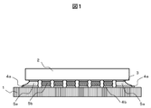
- FIG. 1 is a cross-sectional view of a semiconductor device of Example 1;
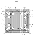
- FIG. 1 is a plan view of a semiconductor device of Example 1;
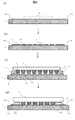
- FIG. 7 is a cross-sectional view showing the manufacturing process of the semiconductor device of Example 1;
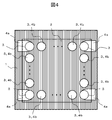
- FIG. 7 is a plan view of the semiconductor device of Example 2;
- FIG. 7 is a plan view of the semiconductor device of Example 2;
- FIG. 10 is a plan view of the semiconductor device of Example 3;
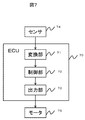
- FIG. 14 is a block diagram of an electronic control unit of a fourth embodiment.
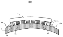
- FIG. 14 is a cross-sectional view of a semiconductor device mounted on the electronic control unit of the fourth embodiment.
- the electrodes and solder balls of the area array type package type semiconductor device are formed in advance by a package maker, and the composition of the solder balls is generally Sn-3.0Ag-0.5Cu.
- solder bumps can be arranged in large numbers within a given area by reducing the size and pitch, which is advantageous for downsizing and densification.
- the wiring length is shorter than the structure connected through the leads, it is advantageous for high-speed transmission, and high performance can be achieved.
- a Si chip which is a semiconductor element is connected to an interposer by, for example, a wire. Electrodes and solder balls are formed on the back surface of the interposer, and the structure on the interposer is molded with resin. Although this is connected to the wiring substrate through the solder bumps, it is deformed at the time of temperature load due to the difference in coefficient of linear expansion of each component and stress is applied to the solder bumps on the outermost periphery of the BGA package.
- the load on the solder bumps at the outermost corners of the BGA package is large, and in these solder bumps, crack extension occurs notably at the interface with the electrodes on the upper side of the solder bumps, which causes a reduction in thermal fatigue life. .
- the stress applied to the solder bumps in the outermost peripheral corner portion is reduced to prevent the thermal fatigue life from being reduced.
- the semiconductor device of the first embodiment will be described with reference to FIGS. 1 to 3.
- the semiconductor device has a wiring substrate 1 and a semiconductor package (area array type package) 2.
- the wiring substrate 1 has a plurality of electrodes 4 on the top surface.
- the semiconductor package 2 has a plurality of electrodes 3 on the lower surface.
- the semiconductor package 2 is mounted opposite to the wiring board 1 via solder joints (bumps) 5 connecting the plurality of electrodes 4 and the plurality of electrodes 3.
- the electrodes 4 formed on the upper surface of the wiring substrate 1 are uniformly formed to face the electrodes 3 provided on the lower surface of the semiconductor package 2.
- the solder joints 5b other than the outermost corner have a drum-shaped bump shape.
- the solder joint portion 5 a disposed at the outermost corner portion has a fillet shape extending outward beyond the outer peripheral end portion of the semiconductor package 2.
- the front end portions of the four electrodes 4 a at the outermost peripheral corner portions are located outside the outer peripheral end portion of the semiconductor package 2. Therefore, the front end portion of the solder joint portion 5 a at the outermost peripheral corner portion is also positioned outside the outer peripheral end portion of the semiconductor package 2.
- the semiconductor package 2 is mounted on the wiring substrate 1.
- the electrodes 4 b on the wiring substrate other than the outermost corner portion are arranged in a circular shape so as to correspond to the electrodes 3 provided on the lower surface of the semiconductor package 2.
- the size of the electrode 4 b may be the same as that of the electrode 3 or may not be the same from the viewpoint of production, and may be appropriately designed.
- the shape of the electrode 4 a on the wiring substrate 1 at the outermost peripheral corner portion is such that the end portion entering the inside of the semiconductor package 2 is circular and the corner portion is shaped at the end portion extending outside the semiconductor package 2. I have it.
- the present invention is not limited to this shape, as long as the tip of the electrode 4 a on the wiring substrate 1 at the outermost corner is out on the periphery of the semiconductor package 2. It is also possible to make it circular and to make the shape of the electrode 4a elliptical.
- the tip end of the electrode 4 a disposed at the outermost corner of the wiring substrate 1 is located outside the outer peripheral end of the semiconductor package 2. Further, the tip end of the solder joint 5 a disposed at the outermost corner of the wiring board 1 is also located outside the outer peripheral end of the semiconductor package 2.
- the area of the electrode 4 a disposed in the outermost peripheral corner of the wiring substrate 1 is larger than the area of the electrode 3 disposed in the outermost peripheral corner of the semiconductor package 2. Furthermore, the area of the electrode 4 a disposed at the outermost corner of the wiring board 1 is larger than the area of the electrode 4 b disposed at other than the outermost corner of the wiring board 1.
- the center 9 b of the electrode 4 a disposed at the outermost corner of the wiring substrate 1 is closer to the semiconductor package than the center 9 a of the electrode 3 disposed at the outermost corner of the semiconductor package 2. It is shifted in the direction from the center of 2 toward the outside.
- the shape of the solder joint portion 5 a disposed at the outermost peripheral corner portion of the wiring substrate 1 is different from the shape of the solder joint portion 5 b disposed at other than the outermost peripheral corner portion of the wiring substrate 1.
- the solder joint portion 5 a disposed at the outermost peripheral corner portion of the wiring substrate 1 has a fillet shape extending outward beyond the outer peripheral end portion of the semiconductor package 2.
- the solder joint portion 5 b disposed other than the outermost peripheral corner portion of the wiring board 1 has a drum-shaped shape.
- the electrodes 4 a disposed at the outermost peripheral corner of the wiring substrate 1 are disposed on the diagonal of the outermost peripheral corner.
- a plurality of electrodes 4 are formed on the wiring substrate 1 (see FIG. 3A).
- the wiring board 1 has an electrode 4 on the top surface thereof.
- the electrode 4 has an area different from that of the electrode 4a at the outermost peripheral corner and the other electrode 4b, and the area of the electrode 4a is larger than the area of the electrode 4b.
- the solder 6 is formed on the electrode 4 on the wiring substrate 1 (see FIG. 3B).
- the acceptance solder 6 may be formed by printing or may be applied by a dispenser, and the formation method is not limited to these.
- the composition of the solder 6 may be the same as or different from the solder balls 7 formed in advance on the semiconductor package 2. It is comprehensively judged from the viewpoint of bonding property, productivity and reliability of electronic parts other than the semiconductor package 2 mounted on the wiring substrate 1.
- the semiconductor package 2 is mounted on the formation site of the solder 6 using a mounting machine (not shown). Then, a metal piece 8 containing any of Bi, In, and Sb or a plurality of elements is mounted on the electrode 4a on the wiring substrate 1 corresponding to the outermost corner of the semiconductor package 2 (see FIG. 3C). At this time, it is desirable from the viewpoint of productivity that the metal piece 8 also has a chip-type solder shape that can be reel-mounted by the mounting machine.
- the volume of the metal piece 8 mounted on the electrode 4a is determined by calculation from the volume of the solder ball 7 provided on the semiconductor package 2 and the area of the electrode 4a. Note that the semiconductor package 2 may be mounted after the metal piece 8 is mounted, and the mounting order thereof is appropriately determined.
- the semiconductor package 2 and the wiring substrate 1 on which the metal pieces 8 are mounted are heated using a reflow furnace (not shown) to melt the solder balls 7, the solder 6 and the metal pieces 8. Thereafter, the semiconductor package 2 and the wiring substrate 1 are bonded by cooling (see FIG. 3D).
- the solder joint 5a at the outermost peripheral corner of the semiconductor package 2 and the other solder joints 5b have different metal compositions of the solder joint. Specifically, the concentration of at least one element of Bi, In, and Sb is higher in the solder joint portion 5a at the outermost peripheral corner portion than in the solder joint portion 5b.
- Bi, In, and Sb are elements that improve the thermal fatigue life.
- the solder joint portion 5a at the outermost peripheral corner portion of the semiconductor package 2 can be easily changed to a long life composition unlike the composition of the other solder joint portions 5b. Thus, the semiconductor device shown in FIG. 1 is completed.
- Example 1 by melting the metal piece 8 containing any one or more elements of Bi, In, Sb, a semiconductor package in which any one or more metals of Bi, In, Sb or the main composition is SnAgCu It diffuses only to the solder joint portion 5 a of the outermost peripheral corner portion 2. Thereby, the thermal fatigue life can be extended.
- the solder joint portion 5a at the outermost peripheral corner portion becomes a fillet shape, thereby changing the way of applying stress and suppressing crack propagation.
- the stress at the solder joint portion 5 a at the outermost peripheral corner portion of the semiconductor package 2 can be reduced, and the reliability when mounting the semiconductor package 2 can be improved.
- the first embodiment it is possible to change the solder composition of the solder joint portion 5a of the outermost peripheral corner without changing the solder composition of the solder ball 7 itself of the semiconductor package 2.
- the manufacturing cost can be reduced.
- composition of the solder joint 5 is a general Sn-3Ag-0.5Cu
- composition of the solder joint 5a is Sn-3Ag-3Bi-3In
- composition of the solder joint 5b is Thermal stress analysis was performed on two patterns of model B, which is Sn-3Ag-0.5Cu.
- the composition of the solder joint portion 5 is general Sn-3Ag-0.5Cu.
- the tip of the electrode 4a is outside the outer peripheral end of the semiconductor package 2 and the solder joint 5a at the outermost corner is fillet-shaped, and the composition of the solder joint 5a is Sn -3Ag-3Bi-3In, and the composition of the solder joint 5b is Sn-3Ag-0.5Cu.
- the model A and the model B are all the same except for the size of the electrode 4a and the shape and composition of the solder joint 5a at the outermost corner.
- the thermal fatigue life of the solder joint 5a at the outermost peripheral corner of the model B is, in an analysis result obtained by applying a thermal load simulating a temperature cycle test repeating -40 ° C and 125 ° C to the model A and the model B,
- the thermal fatigue life of the solder joint portion 5a at the outermost peripheral corner portion of the model A was 1.9 times as large as that of the thermal fatigue life. Also from the result of the thermal stress analysis, it is understood that the thermal fatigue life is improved in the first embodiment.
- the semiconductor device of the second embodiment will be described with reference to FIGS. 4 and 5.
- the electrodes 4a of the wiring electrodes 1 corresponding to the outermost peripheral corner portion of the semiconductor package 2 are arranged on the diagonal of the corner.
- the electrode 4 a of the wiring electrode 1 corresponding to the outermost peripheral corner of the semiconductor package 2 is on the extension of the opposing side of the semiconductor package 2 in the vertical direction. It is pulled out.
- the solder joint portion 5 a at the outermost peripheral corner portion has a fillet shape having a long side in the vertical direction of the opposing side of the semiconductor package 2.
- the outer end of the electrode 4 c at the outermost periphery of the opposing side of the semiconductor package 2 is extended outside the outer periphery of the semiconductor package 2.
- the solder joint on the outermost periphery of the opposite side of the is made into a fillet shape.
- the composition of the solder joints 5a on the outermost periphery of the opposing sides of the semiconductor package 2 in the fillet shape is at least one of Bi, In and Sb than the other solder joints 5b.
- the concentration of elements is high.
- the other configuration is the same as that of the semiconductor device of the first embodiment, and hence the description thereof is omitted.
- the outer end of the electrode 4 a of the wiring electrode 1 corresponding to the outermost peripheral corner of the semiconductor package 2 is drawn on the diagonal of the corner.
- the outermost electrodes 4c of the opposing sides are drawn on the vertical extension lines of the opposing sides of the semiconductor package 2.
- the solder joint portion 5a at the outermost peripheral corner portion has a fillet shape having long sides in the diagonal direction of the corner portion, and the solder joint portion at the outermost peripheral portion is perpendicular to the opposing side of the semiconductor package 2 It has a fillet shape with long sides.
- the solder joint portion 5a at the outermost peripheral corner portion does not have to be a fillet shape having a long side in the diagonal direction of the corner portion, and a fillet having a long side in the vertical direction of either opposing side of the semiconductor package 2 It may be a shape.
- the composition of the solder bond 5a at the outermost periphery of the semiconductor package 2 in the fillet shape has a higher concentration of at least one of Bi, In, and Sb than the other solder connection parts 5b. .
- the other configuration is the same as that of the semiconductor device of the first embodiment, and hence the description thereof is omitted.
- the electronic control unit (ECU) 70 includes a conversion unit 71, a control unit 72, and an output unit 73, and has a function of transmitting a signal from the sensor unit 74 to the motor unit 75.
- the semiconductor device of the first embodiment is mounted on the control unit 72 of the electronic control unit 70.
- an engine control unit is a microcontroller (microcomputer) that comprehensively controls engine operation control when using an electrical auxiliary device.
- the on-board electronic control unit 70 is exposed to the ambient temperature and repeats in the high temperature environment and the low temperature environment. In the cabin as well, the engine reaches about 50 ° C. while the engine is stopped, and in cold regions, it is exposed to below freezing. In the electronic control unit 70 installed in the engine room, the maximum environmental temperature is 100 ° C. or higher.
- a state in which the semiconductor device of the first embodiment mounted on the electronic control unit 70 is placed in an environment where high temperature and low temperature are repeated will be described with reference to FIG.
- the linear expansion coefficients of the wiring substrate 1 mainly using an organic substrate and the semiconductor package 2 mounted on the wiring substrate 1 are different. For this reason, in the environment where high temperature and low temperature are repeated, the respective warpage amounts differ, and a large load is applied to the solder joint portion 5 a at the outermost peripheral corner portion of the semiconductor package 2. For this reason, the fact that the connection length of the solder joint portion 5a at the outermost peripheral corner portion is long is effective for the thermal fatigue life until the crack growth and fracture of the solder joint portion 5a.
Landscapes
- Engineering & Computer Science (AREA)
- Microelectronics & Electronic Packaging (AREA)
- Power Engineering (AREA)
- Mechanical Engineering (AREA)
- Chemical & Material Sciences (AREA)
- Combustion & Propulsion (AREA)
- Transportation (AREA)
- Manufacturing & Machinery (AREA)
- Wire Bonding (AREA)
- Electric Connection Of Electric Components To Printed Circuits (AREA)
- Structures For Mounting Electric Components On Printed Circuit Boards (AREA)
- Physics & Mathematics (AREA)
- Geometry (AREA)
Abstract
モータを制御する制御部は半導体装置を有し、半導体装置は、複数の第1の電極を有する半導体パッケージと、複数の第1の電極のそれぞれに対応するように配置された複数の第2の電極を有する配線基板と、第1の電極と第2の電極とを接続するはんだ接合部とを有し、配線基板の最外周角部に配置された第2の電極の先端部は半導体パッケージの外周端部よりも外側に位置する。
Description
本発明は、電子制御装置に関する。
近年、電子機器の小型化、高密度化及び高機能化に伴い、半導体装置にも小型化及び高密度化が要求されている。このため、半導体装置として、BGA(Ball Grid Array)やCSP(Chip Size Package)のようなエリアアレイ型のパッケージ型半導体装置が多く利用されている。
エリアアレイ型のパッケージ型半導体装置は、裏面に電極及びはんだボールが一定のサイズ、面積及びピッチで形成されている。これらの電極及びはんだボールに対応するように配線基板の電極も一定のサイズ、面積及びピッチで形成されている。そして、配線基板にパッケージ型半導体装置を搭載して加熱することによりはんだバンプを形成して対応する電極同士が接合される。
例えば、特許文献1には、BGAパッケージと配線基板との接続において、配線基板の最外周電極のうち、最もアレイ状配列の外側に位置する端部が、BGAパッケージ側の最外周電極のうち、最もアレイ状配列の外側に位置する端部よりもアレイ状配列の外側に位置し、配線基板の電極表面とはんだバンプ表面とがなす角度を鋭角にする構造が開示されている。
エリアアレイ型のパッケージ型半導体装置は、各構成部材の線膨張係数の違いにより温度負荷時に変形し、最外周のはんだバンプに応力がかかる。
特に、BGAパッケージの最外周角部のはんだバンプへの負荷が大きく、これらのはんだバンプにおいて、亀裂伸展がとりわけはんだバンプ上側の電極との界面で顕著に起こり熱疲労寿命が低下する。
具体的には、エリアアレイ型パッケージをはんだバンプを介して配線基板に接続する半導体装置においては、使用環境下での温度変化により半導体装置全体が変形する。しかし、それぞれの構成部材は線膨張係数の違いにより反り量がそれぞれ異なり、エリアアレイ型パッケージと配線基板間のはんだバンプに亀裂伸展が起こる。特に、エリアアレイ型パッケージの最外周角部のはんだバンプが壊れやすく、熱疲労寿命が低下して半導体装置の信頼性が低下する。
特許文献1には、外部衝撃時における最外周はんだバンプにかかる応力を緩和することについては言及されている。しかし、構成部材の線膨張係数の違いにより反り量がそれぞれ異なり、これが原因で熱疲労寿命に影響を与えることについては考慮されていない。
本発明の目的は、半導体装置を内蔵した電子制御装置において、熱疲労寿命が低下することを防止することにある。
本発明の一態様の電子制御装置は、モータを制御する制御部を備え、前記制御部は半導体装置を有し、前記半導体装置は、複数の第1の電極を有する半導体パッケージと、前記複数の第1の電極のそれぞれに対応するように配置された複数の第2の電極を有する配線基板と、前記第1の電極と前記第2の電極とを接続するはんだ接合部とを有し、前記配線基板の最外周角部に配置された前記第2の電極の先端部は、前記半導体パッケージの外周端部よりも外側に位置することを特徴とする。
本発明の一態様によれば、半導体装置を内蔵した電子制御装置において、熱疲労寿命が低下することを防止することにある。
エリアアレイ型のパッケージ型半導体装置(半導体パッケージ)の電極及びはんだボールは、パッケージメーカによりあらかじめ形成されており、はんだボールの組成は、Sn-3.0Ag-0.5Cuが一般的である。
はんだバンプは、サイズ及びピッチを小さくすることで、一定面積内に多数配置することが可能であり、小型化及び高密度化に有利である。また、リードを介して接続する構造よりも配線長が短いため、高速伝送に有利であり高性能化を達成できる。
エリアアレイ型のパッケージ型半導体装置のBGAパッケージは、半導体素子であるSiチップが、例えばワイヤでインターポーザに接続されている。インターポーザの裏面には、電極及びはんだボールが形成され、インターポーザ上を樹脂でモールドした構造を有する。これを配線基板にはんだバンプを介して接続するが、各構成部材の線膨張係数の違いにより、温度負荷時に変形し、BGAパッケージの最外周のはんだバンプに応力がかかる。
特に、BGAパッケージの最外周角部のはんだバンプへの負荷が大きく、これらのはんだバンプにおいて、亀裂伸展がとりわけはんだバンプ上側の電極との界面で顕著に起こり、熱疲労寿命が低下する要因となる。
以下の実施例では、エリアアレイ型パッケージをはんだバンプを介して配線基板に接続する半導体装置において、最外周角部のはんだバンプにかかる応力を低減して熱疲労寿命が低下するのを防止する。
以下、図面を参照して実施例について説明する。
図1~図3を参照して、実施例1の半導体装置について説明する。
図1に示すように、半導体装置は、配線基板1と半導体パッケージ(エリアアレイ型パッケージ)2を有する。配線基板1は、上面に複数の電極4を有する。半導体パッケージ2は、下面に複数の電極3を有する。半導体パッケージ2は、複数の電極4との複数の電極3とを接続するはんだ接合部(バンプ)5を介して配線基板1に対向して実装される。
配線基板1の上面に形成される電極4のうち、最外周角部以外の電極4bは、半導体パッケージ2の下面に備える電極3に対向するように一様に形成されている。最外周角部以外のはんだ接合部5bは太鼓型のバンプ形状を有する。最外周角部に配置されたはんだ接合部5aは、半導体パッケージ2の外周端部よりも外側に延伸したフィレット形状を有する。
最外周角部の4つの電極4aの先端部は、半導体パッケージ2の外周端部よりも外側に位置している。そのため、最外周角部のはんだ接合部5aの先端部も、半導体パッケージ2の外周端部よりも外側に位置している。
図2に示すように、配線基板1の上に半導体パッケージ2が実装されている。最外周角部以外の配線基板上の電極4bは、半導体パッケージ2の下面に設けられた電極3に対応するように円形形状で配置される。電極4bのサイズは、電極3と同一でも良いし、生産上の観点から同一でなくても良く、適宜設計されれば良い。
図2に示すように、最外周角部の配線基板1上の電極4aの形状を、半導体パッケージ2の内側に入る端部を円形とし、半導体パッケージ2の外側に出る端部の形状に角を持たせている。しかし、この形状に限定されるものではなく、最外周角部の配線基板1上の電極4aの先端部が半導体パッケージ2の外周に出ていればよく、半導体パッケージ2の外側に出る端部も円形とし、電極4aの形状を楕円とすることも可能である。
このように、実施例1の半導体装置は、配線基板1の最外周角部に配置された電極4aの先端部は、半導体パッケージ2の外周端部よりも外側に位置する。さらに、配線基板1の最外周角部に配置されたはんだ接合部5aの先端部も、半導体パッケージ2の外周端部よりも外側に位置する。
さらに、配線基板1の最外周角部に配置された電極4aの面積は、半導体パッケージ2の最外周角部に配置された電極3の面積よりも大きい。さらに、配線基板1の最外周角部に配置された電極4aの面積は、配線基板1の最外周角部以外に配置された電極4bの面積よりも大きい。
さらに、図2に示すように、配線基板1の最外周角部に配置された電極4aの中心9bは、半導体パッケージ2の最外周角部に配置された電極3の中心9aよりも、半導体パッケージ2の中心から外側に向かう方向にずれている。
また、配線基板1の最外周角部に配置されたはんだ接合部5aの形状は、配線基板1の最外周角部以外に配置されたはんだ接合部5bの形状とは異なる。具体的には、配線基板1の最外周角部に配置されたはんだ接合部5aは、半導体パッケージ2の外周端部よりも外側に延伸したフィレット形状を有する。配線基板1の最外周角部以外に配置されたはんだ接合部5bは、太鼓型の形状を有する。
また、図2に示すように、配線基板1の最外周角部に配置された電極4aは、最外周角部の対角線上に配置されている。
次に、図3を参照して、実施例1の半導体装置の製造工程について説明する。
まず、配線基板1の上に複数の電極4を形成する(図3(a)参照)。ここで、配線基板1は、その上面に電極4を有する。電極4は、最外周角部の電極4aとそれ以外の電極4bとは異なる面積を有し、電極4aの面積は電極4bの面積より大きい。
次に、配線基板1上の電極4に迎えはんだ6を形成する(図3(b)参照)。この際、迎えはんだ6は、印刷により形成しても良いし、ディスペンサーで塗布しても良く、その形成手法はこれらに限定されるものではない。迎えはんだ6の組成は、半導体パッケージ2にあらかじめ形成されているはんだボール7と同一でも良いし、異なっていても良い。配線基板1に搭載される半導体パッケージ2以外の電子部品の接合性、生産性及び信頼性の観点から総合的に判断される。
迎えはんだ6の形成箇所に、搭載機(図示せず)を用いて半導体パッケージ2を搭載する。そして、半導体パッケージ2の最外周角部にあたる配線基板1上の電極4aには、Bi、In、Sbのいずれかもしくは複数の元素を含む金属片8を搭載する(図3(c)参照)。この際、金属片8も搭載機にてリール搭載できるチップ型はんだ形状を有することが生産性の観点で望ましい。
電極4aに搭載する金属片8の体積は、半導体パッケージ2に備えられたはんだボール7の体積及び電極4aの面積から算出して決定される。なお、金属片8を搭載した後に、半導体パッケージ2を搭載しても良く、その搭載順は適宜決定される。
次に、半導体パッケージ2と、金属片8が搭載された配線基板1とをリフロー炉(図示せず)を用いて加熱し、はんだボール7と迎えはんだ6及び金属片8を溶融させる。その後、冷却することにより半導体パッケージ2と配線基板1が接合される(図3(d)参照)。この際、半導体パッケージ2の最外周角部のはんだ接合部5aとそれ以外のはんだ接合部5bは、はんだ接合部の金属組成が異なる。具体的には、最外周角部のはんだ接合部5aは、Bi、In、Sbの少なくとも何れか一つの元素の濃度は、はんだ接合部5bよりも高くなる。ここで、Bi、In、Sbは、熱疲労寿命を向上させる元素である。半導体パッケージ2の最外周角部のはんだ接合部5aは、それ以外のはんだ接合部5bの組成と異なり、簡便に長寿命組成に変更することができる。このようにして、図1に示す半導体装置が完成する。
実施例1では、Bi、In、Sbのいずれかもしくは複数の元素を含む金属片8を溶融させることにより、Bi、In、Sbのいずれかもしくは複数の金属が、主組成がSnAgCuである半導体パッケージ2の最外周角部のはんだ接合部5aのみに拡散する。これにより、熱疲労寿命を長寿命化できる。
また、実施例1では、金属片8を溶融させることにより、容易に最外周角部のはんだ接合部5aの体積を増大させることができる。これにより、最外周角部のはんだ接合部5aがフィレット形状になることで応力のかかり方が変わり、クラック進展を抑制できる。この結果、半導体パッケージ2の最外周角部のはんだ接合部5aの応力が低減し、半導体パッケージ2を実装する際の信頼性を向上させることができる。
さらに、実施例1では、半導体パッケージ2のはんだボール7自体のはんだ組成を変更することなく、最外周角部のはんだ接合部5aのはんだ組成を変更可能である。この結果、市販品の半導体パッケージ2を利用できるため、製造コストを削減することができる。
ここで、はんだ接合部5の組成が一般的なSn-3Ag-0.5CuであるモデルAと、はんだ接合部5aの組成がSn-3Ag-3Bi-3Inであり、はんだ接合部5bの組成がSn-3Ag-0.5CuであるモデルBの2パターンにおいて熱応力解析を実施した。
ここで、モデルAは、配線基板1上に形成される電極4aと電極4bの面積が同一で、半導体パッケージ2の最外周角部のはんだ接合部5aとそれ以外のはんだ接合部5bの形状が同一のバンプ形状を有る構造において、はんだ接合部5の組成が一般的なSn-3Ag-0.5Cuである。一方、モデルBは、電極4aの先端部を半導体パッケージ2の外周端部よりも外側にし、最外周角部のはんだ接合部5aをフィレット形状とした構造において、そのはんだ接合部5aの組成がSn-3Ag-3Bi-3Inであり、はんだ接合部5bの組成がSn-3Ag-0.5Cuである。電極4aのサイズ及び最外周角部のはんだ接合部5aの形状及び組成以外は、モデルA、モデルBともに全て同一である。
モデルA、モデルBに対して、-40℃と125℃を繰り返す温度サイクル試験を模擬した熱負荷を与えた解析結果において、モデルBの最外周角部のはんだ接合部5aの熱疲労寿命は、モデルAの最外周角部のはんだ接合部5aの熱疲労寿命に比べて1.9倍となった。この熱応力解析の結果からも、実施例1では、熱疲労寿命が向上することが分かる。
図4、図5を参照して、実施例2の半導体装置について説明する。
図2に示す実施例1の半導体装置では、半導体パッケージ2の最外周角部に対応する配線電極1の電極4aは、角の対角線上に配置されている。これに対して、図4に示す実施例2の半導体装置では、半導体パッケージ2の最外周角部に対応する配線電極1の電極4aは、半導体パッケージ2の対向する辺の垂直方向の延長線上に引き出されている。この場合、最外周角部のはんだ接合部5aは、半導体パッケージ2の対向する辺の垂直方向に長辺があるフィレット形状となる。
また、図5に示すように、最外周角部の電極4aに加えて、半導体パッケージ2の対向する辺の最外周の電極4cの外側端部を半導体パッケージ2の外周外側に出し、半導体パッケージ2の対向する辺の最外周にあるはんだ接合部をフィレット形状とする。
図4、図5において、フィレット形状となる半導体パッケージ2の対向する辺の最外周のはんだ接合部5aの組成は、それ以外のはんだ接合部5bよりもBi、In、Sbの少なくとも何れか一つの元素の濃度が高くなっている。
それ以外の構成については、実施例1の半導体装置と同様なのでその説明は省略する。
図6を参照して、実施例3の半導体装置について説明する。
図6に示すように、実施例3の半導体装置は、半導体パッケージ2の最外周角部に対応する配線電極1の電極4aは、その外側端部を角の対角線上に出し、半導体パッケージ2の対向するそれぞれの辺の最外周の電極4cを、半導体パッケージ2の対向する辺のそれぞれの垂直方向の延長線上に引き出す。
この場合、最外周角部のはんだ接合部5aは、角部の対角方向に長辺があるフィレット形状となり、それ以外の最外周のはんだ接合部は、半導体パッケージ2の対向する辺の垂直方向に長辺があるフィレット形状となる。
なお、最外周角部のはんだ接合部5aは、角部の対角方向に長辺があるフィレット形状でなくとも良く、半導体パッケージ2の対向するどちらかの辺の垂直方向に長辺があるフィレット形状であっても良い。
図6において、フィレット形状となる半導体パッケージ2の最外周のはんだ接合5aの組成は、それ以外のはんだ接続部5bよりもBi、In、Sbの少なくとも何れか一つの元素の濃度が高くなっている。
それ以外の構成については、実施例1の半導体装置と同様なのでその説明は省略する。
図7、図8を参照して、実施例1の半導体装置を有する電子制御装置について説明する。
車載向けの電子機器においては、車室内空間確保の観点からも、その設置環境が車室内からエンジンルーム内へと変遷しており、より高温環境下での耐性が求められている。また、車両寿命の延伸から、電子機器においても長寿命化が求められている。
図7を参照して、実施例4の電子制御装置について説明する。
図7に示すように、電子制御装置(ECU)70は、変換部71、制御部72、出力部73を備えており、センサ部74からの信号をモータ部75に伝達する機能を備えている。電子制御装置70の制御部72に実施例1の半導体装置が搭載されている。
ここで、エンジンコントロールユニット(engine control unit、ECU)とは、エンジンの運転制御を電気的な補助装置を用いて行う際に、それらを総合的に制御するマイクロコントローラ(マイコン)である。
車載用途の電子制御装置70は、環境温度にさらされ、高温環境と低温環境に繰り返す。車室内においても、エンジン停止中では50℃近くに達し、また寒冷地においては氷点下にさらされる。エンジンルーム内に設置される電子制御装置70においては、環境温度の最高が100℃以上になる。
図8を参照して、電子制御装置70に搭載された実施例1の半導体装置が、高温と低温が繰り返される環境に置かれた時の状態について説明する。
主に有機基板が用いられる配線基板1と、配線基板1に搭載される半導体パッケージ2は、それぞれの線膨張係数が異なる。このため、高温と低温が繰り返される環境においてそれぞれの反り量が異なり、半導体パッケージ2の最外周角部のはんだ接合部5aに大きな負荷がかかる。このため、最外周角部のはんだ接合部5aの接続長が長いことは、はんだ接合部5aのクラック進展及び破断までの熱疲労寿命に効果的である。
主に有機基板が用いられる配線基板1と、配線基板1に搭載される半導体パッケージ2は、それぞれの線膨張係数が異なる。このため、高温と低温が繰り返される環境においてそれぞれの反り量が異なり、半導体パッケージ2の最外周角部のはんだ接合部5aに大きな負荷がかかる。このため、最外周角部のはんだ接合部5aの接続長が長いことは、はんだ接合部5aのクラック進展及び破断までの熱疲労寿命に効果的である。
1 配線基板
2 半導体パッケージ
3 電極
4a 最外周角部電極
4b 最外周角部以外の電極
5a 最外周角部のはんだ接合部
5b 最外周角部以外のはんだ接合部
70 電子制御装置
71 変換部
72 制御部
73 出力部
74 センサ部
75 モータ部
2 半導体パッケージ
3 電極
4a 最外周角部電極
4b 最外周角部以外の電極
5a 最外周角部のはんだ接合部
5b 最外周角部以外のはんだ接合部
70 電子制御装置
71 変換部
72 制御部
73 出力部
74 センサ部
75 モータ部
Claims (12)
- モータを制御する制御部を備えた電子制御装置であって、
前記制御部は、半導体装置を有し、
前記半導体装置は、
複数の第1の電極を有する半導体パッケージと、
前記複数の第1の電極のそれぞれに対応するように配置された複数の第2の電極を有する配線基板と、
前記第1の電極と前記第2の電極とを接続するはんだ接合部と、を有し、
前記配線基板の最外周角部に配置された前記第2の電極の先端部は、前記半導体パッケージの外周端部よりも外側に位置することを特徴とする電子制御装置。 - 前記配線基板の前記最外周角部に配置された前記はんだ接合部の先端部は、前記半導体パッケージの外周端部よりも外側に位置することを特徴とする請求項1に記載の電子制御装置。
- 前記配線基板の最外周角部に配置された前記第2の電極の面積は、前記半導体パッケージの最外周角部に配置された前記第1の電極の面積よりも大きいことを特徴とする請求項2に記載の電子制御装置。
- 前記配線基板の最外周角部に配置された前記第2の電極の面積は、前記配線基板の最外周角部以外に配置された前記第2の電極の面積よりも大きいことを特徴とする請求項3に記載の電子制御装置。
- 前記配線基板の最外周角部に配置された前記第2の電極の中心は、前記半導体パッケージの最外周角部に配置された前記第1の電極の中心よりも、前記半導体パッケージの中心から外側に向かう方向にずれていることを特徴とする請求項4に記載の電子制御装置。
- 前記配線基板の最外周角部に配置された前記はんだ接合部の形状は、前記配線基板の最外周角部以外に配置された前記はんだ接合部の形状とは異なることを特徴とする請求項1に記載の電子制御装置。
- 前記配線基板の最外周角部に配置された前記はんだ接合部は、前記半導体パッケージの外周端部よりも外側に延伸したフィレット形状を有することを特徴とする請求項6に記載の電子制御装置。
- 前記配線基板の最外周角部に配置された前記第2の電極は、前記最外周角部の対角線上に配置されていることを特徴とする請求項1に記載の電子制御装置。
- 前記配線基板の最外周角部に配置された前記第2の電極は、前記半導体パッケージの対向する辺の垂直方向の延長線上に引き出されていることを特徴とする請求項1に記載の電子制御装置。
- 前記配線基板の最外周角部に配置された前記はんだ接合部の組成は、前記配線基板の最外周角部以外に配置された前記はんだ接合部の組成とは異なり、
前記配線基板の最外周角部に配置された前記はんだ接合部は、Bi、In及びSbの内の少なくとも一つの元素を含み、
前記最外周角部に配置された前記はんだ接合部の前記元素の濃度は、前記配線基板の最外周角部以外に配置された前記はんだ接合部に含まれるBi、In、Sbの内の少なくとも一つの元素の濃度よりも高いことを特徴とする請求項1に記載の電子制御装置。 - 前記制御部の前記半導体装置は、車載向けの電子機器に搭載されていることを特徴とする請求項1に記載の電子制御装置。
- 前記配線基板と前記半導体パッケージは、線膨張係数がそれぞれ異なり、
前記車載向けの電子機器においては、高温と低温が繰り返される環境下で前記配線基板と前記半導体パッケージの反り量がそれぞれ異なり、
前記配線基板の最外周角部に配置された前記はんだ接合部にかかる負荷は、前記配線基板の最外周角部以外に配置された前記はんだ接合部にかかる負荷よりも大きいことを特徴とする請求項11に記載の電子制御装置。
Priority Applications (2)
| Application Number | Priority Date | Filing Date | Title |
|---|---|---|---|
| US16/754,326 US20200243470A1 (en) | 2017-10-10 | 2018-09-11 | Electronic control device |
| CN201880065755.6A CN111194478A (zh) | 2017-10-10 | 2018-09-11 | 电子控制装置 |
Applications Claiming Priority (2)
| Application Number | Priority Date | Filing Date | Title |
|---|---|---|---|
| JP2017-196587 | 2017-10-10 | ||
| JP2017196587A JP6955954B2 (ja) | 2017-10-10 | 2017-10-10 | 電子制御装置 |
Publications (1)
| Publication Number | Publication Date |
|---|---|
| WO2019073734A1 true WO2019073734A1 (ja) | 2019-04-18 |
Family
ID=66100510
Family Applications (1)
| Application Number | Title | Priority Date | Filing Date |
|---|---|---|---|
| PCT/JP2018/033563 Ceased WO2019073734A1 (ja) | 2017-10-10 | 2018-09-11 | 電子制御装置 |
Country Status (4)
| Country | Link |
|---|---|
| US (1) | US20200243470A1 (ja) |
| JP (1) | JP6955954B2 (ja) |
| CN (1) | CN111194478A (ja) |
| WO (1) | WO2019073734A1 (ja) |
Families Citing this family (5)
| Publication number | Priority date | Publication date | Assignee | Title |
|---|---|---|---|---|
| JP7490974B2 (ja) | 2020-02-05 | 2024-05-28 | 富士電機株式会社 | 半導体モジュール及び半導体モジュールの製造方法 |
| CN111863759B (zh) | 2020-03-26 | 2025-08-19 | 北京小米移动软件有限公司 | 芯片、电路板、电路板组件及电子设备 |
| JP7524632B2 (ja) * | 2020-06-29 | 2024-07-30 | 日本電気株式会社 | 量子デバイス |
| CN113921491A (zh) | 2020-07-08 | 2022-01-11 | 北京小米移动软件有限公司 | 芯片、电路板及电子设备 |
| DE102023126557B3 (de) * | 2023-09-28 | 2024-12-05 | Phytec Meßtechnik GmbH | Lötplatinenanordnung |
Citations (6)
| Publication number | Priority date | Publication date | Assignee | Title |
|---|---|---|---|---|
| JPH11121525A (ja) * | 1997-10-20 | 1999-04-30 | Sony Corp | 半導体装置 |
| JP2000114315A (ja) * | 1998-09-29 | 2000-04-21 | Denso Corp | 電子部品の実装構造 |
| JP2000195982A (ja) * | 1998-12-28 | 2000-07-14 | Pfu Ltd | 小型半導体装置および小型半導体装置の実装構造ならびにセラミック基板の製造方法 |
| JP2003197813A (ja) * | 2001-12-28 | 2003-07-11 | Mitsubishi Electric Corp | 電子装置 |
| JP2007251053A (ja) * | 2006-03-17 | 2007-09-27 | Fujitsu Ltd | 半導体装置の実装構造及びその実装構造の製造方法 |
| JP2015176940A (ja) * | 2014-03-14 | 2015-10-05 | 日立オートモティブシステムズ株式会社 | 半導体装置の実装構造 |
Family Cites Families (1)
| Publication number | Priority date | Publication date | Assignee | Title |
|---|---|---|---|---|
| JPWO2015072294A1 (ja) * | 2013-11-12 | 2017-03-16 | 日立オートモティブシステムズ株式会社 | 車載電子制御装置の放熱構造 |
-
2017
- 2017-10-10 JP JP2017196587A patent/JP6955954B2/ja not_active Expired - Fee Related
-
2018
- 2018-09-11 CN CN201880065755.6A patent/CN111194478A/zh active Pending
- 2018-09-11 WO PCT/JP2018/033563 patent/WO2019073734A1/ja not_active Ceased
- 2018-09-11 US US16/754,326 patent/US20200243470A1/en not_active Abandoned
Patent Citations (6)
| Publication number | Priority date | Publication date | Assignee | Title |
|---|---|---|---|---|
| JPH11121525A (ja) * | 1997-10-20 | 1999-04-30 | Sony Corp | 半導体装置 |
| JP2000114315A (ja) * | 1998-09-29 | 2000-04-21 | Denso Corp | 電子部品の実装構造 |
| JP2000195982A (ja) * | 1998-12-28 | 2000-07-14 | Pfu Ltd | 小型半導体装置および小型半導体装置の実装構造ならびにセラミック基板の製造方法 |
| JP2003197813A (ja) * | 2001-12-28 | 2003-07-11 | Mitsubishi Electric Corp | 電子装置 |
| JP2007251053A (ja) * | 2006-03-17 | 2007-09-27 | Fujitsu Ltd | 半導体装置の実装構造及びその実装構造の製造方法 |
| JP2015176940A (ja) * | 2014-03-14 | 2015-10-05 | 日立オートモティブシステムズ株式会社 | 半導体装置の実装構造 |
Also Published As
| Publication number | Publication date |
|---|---|
| JP2019071345A (ja) | 2019-05-09 |
| US20200243470A1 (en) | 2020-07-30 |
| JP6955954B2 (ja) | 2021-10-27 |
| CN111194478A (zh) | 2020-05-22 |
Similar Documents
| Publication | Publication Date | Title |
|---|---|---|
| JP2019071345A (ja) | 電子制御装置 | |
| WO2009116517A1 (ja) | 電子装置及びその製造方法 | |
| CN1937887A (zh) | 用于减小基板翘曲的结构及方法 | |
| JP2011077108A (ja) | 半導体装置 | |
| JP2008171879A (ja) | プリント基板およびパッケージ実装構造 | |
| JP2006210852A (ja) | 表面実装型回路部品を実装する回路基板及びその製造方法 | |
| JP6015242B2 (ja) | 半導体装置及び回路基板 | |
| JP6489037B2 (ja) | 電子装置及びその製造方法 | |
| JP2009238855A (ja) | 半導体デバイスの実装構造体及び実装構造体を用いた電子機器 | |
| JP2007013099A (ja) | 無鉛半田ボールを有する半導体パッケージ及びその製造方法 | |
| JP2017212266A (ja) | 電子回路装置 | |
| Dhandapani et al. | Improving solder joint reliability for PoP packages in current mobile ecosystem | |
| JP2011159840A (ja) | 電子部品の実装接続構造 | |
| KR100839075B1 (ko) | 아이씨 패키지 및 그 제조방법 | |
| JP5783706B2 (ja) | プリント回路板 | |
| JP4347506B2 (ja) | 半導体装置の実装構造 | |
| CN102473689B (zh) | 具有彼此绝缘电源侧和接地侧金属加固部件的半导体器件 | |
| JP2010050361A (ja) | Lsiパッケージの実装構造、及び電子機器 | |
| JP4128722B2 (ja) | 回路基板および電子機器 | |
| JP2005166886A (ja) | 半導体装置 | |
| JP2006253519A (ja) | 半導体装置 | |
| JP2007027576A (ja) | 半導体装置 | |
| JP2010165852A (ja) | 積層型半導体装置 | |
| JP2009194069A (ja) | 実装済み基板およびその製造方法 | |
| JP2005294469A (ja) | ホール素子の搭載方法 |
Legal Events
| Date | Code | Title | Description |
|---|---|---|---|
| 121 | Ep: the epo has been informed by wipo that ep was designated in this application |
Ref document number: 18865862 Country of ref document: EP Kind code of ref document: A1 |
|
| NENP | Non-entry into the national phase |
Ref country code: DE |
|
| 122 | Ep: pct application non-entry in european phase |
Ref document number: 18865862 Country of ref document: EP Kind code of ref document: A1 |