WO2019066080A1 - 光学フィルムおよび画像表示装置 - Google Patents
光学フィルムおよび画像表示装置 Download PDFInfo
- Publication number
- WO2019066080A1 WO2019066080A1 PCT/JP2018/036603 JP2018036603W WO2019066080A1 WO 2019066080 A1 WO2019066080 A1 WO 2019066080A1 JP 2018036603 W JP2018036603 W JP 2018036603W WO 2019066080 A1 WO2019066080 A1 WO 2019066080A1
- Authority
- WO
- WIPO (PCT)
- Prior art keywords
- optical film
- hard coat
- coat layer
- layer
- inorganic
- Prior art date
- Legal status (The legal status is an assumption and is not a legal conclusion. Google has not performed a legal analysis and makes no representation as to the accuracy of the status listed.)
- Ceased
Links
Images


Classifications
-
- G—PHYSICS
- G02—OPTICS
- G02B—OPTICAL ELEMENTS, SYSTEMS OR APPARATUS
- G02B1/00—Optical elements characterised by the material of which they are made; Optical coatings for optical elements
- G02B1/10—Optical coatings produced by application to, or surface treatment of, optical elements
- G02B1/14—Protective coatings, e.g. hard coatings
-
- B—PERFORMING OPERATIONS; TRANSPORTING
- B32—LAYERED PRODUCTS
- B32B—LAYERED PRODUCTS, i.e. PRODUCTS BUILT-UP OF STRATA OF FLAT OR NON-FLAT, e.g. CELLULAR OR HONEYCOMB, FORM
- B32B27/00—Layered products comprising a layer of synthetic resin
- B32B27/18—Layered products comprising a layer of synthetic resin characterised by the use of special additives
- B32B27/20—Layered products comprising a layer of synthetic resin characterised by the use of special additives using fillers, pigments, thixotroping agents
-
- B—PERFORMING OPERATIONS; TRANSPORTING
- B32—LAYERED PRODUCTS
- B32B—LAYERED PRODUCTS, i.e. PRODUCTS BUILT-UP OF STRATA OF FLAT OR NON-FLAT, e.g. CELLULAR OR HONEYCOMB, FORM
- B32B7/00—Layered products characterised by the relation between layers; Layered products characterised by the relative orientation of features between layers, or by the relative values of a measurable parameter between layers, i.e. products comprising layers having different physical, chemical or physicochemical properties; Layered products characterised by the interconnection of layers
- B32B7/02—Physical, chemical or physicochemical properties
-
- G—PHYSICS
- G09—EDUCATION; CRYPTOGRAPHY; DISPLAY; ADVERTISING; SEALS
- G09F—DISPLAYING; ADVERTISING; SIGNS; LABELS OR NAME-PLATES; SEALS
- G09F9/00—Indicating arrangements for variable information in which the information is built-up on a support by selection or combination of individual elements
-
- H—ELECTRICITY
- H10—SEMICONDUCTOR DEVICES; ELECTRIC SOLID-STATE DEVICES NOT OTHERWISE PROVIDED FOR
- H10K—ORGANIC ELECTRIC SOLID-STATE DEVICES
- H10K50/00—Organic light-emitting devices
- H10K50/80—Constructional details
- H10K50/84—Passivation; Containers; Encapsulations
- H10K50/844—Encapsulations
-
- H—ELECTRICITY
- H10—SEMICONDUCTOR DEVICES; ELECTRIC SOLID-STATE DEVICES NOT OTHERWISE PROVIDED FOR
- H10K—ORGANIC ELECTRIC SOLID-STATE DEVICES
- H10K50/00—Organic light-emitting devices
- H10K50/80—Constructional details
- H10K50/86—Arrangements for improving contrast, e.g. preventing reflection of ambient light
-
- H—ELECTRICITY
- H10—SEMICONDUCTOR DEVICES; ELECTRIC SOLID-STATE DEVICES NOT OTHERWISE PROVIDED FOR
- H10K—ORGANIC ELECTRIC SOLID-STATE DEVICES
- H10K59/00—Integrated devices, or assemblies of multiple devices, comprising at least one organic light-emitting element covered by group H10K50/00
- H10K59/10—OLED displays
- H10K59/12—Active-matrix OLED [AMOLED] displays
-
- H—ELECTRICITY
- H10—SEMICONDUCTOR DEVICES; ELECTRIC SOLID-STATE DEVICES NOT OTHERWISE PROVIDED FOR
- H10K—ORGANIC ELECTRIC SOLID-STATE DEVICES
- H10K59/00—Integrated devices, or assemblies of multiple devices, comprising at least one organic light-emitting element covered by group H10K50/00
- H10K59/40—OLEDs integrated with touch screens
-
- H—ELECTRICITY
- H10—SEMICONDUCTOR DEVICES; ELECTRIC SOLID-STATE DEVICES NOT OTHERWISE PROVIDED FOR
- H10K—ORGANIC ELECTRIC SOLID-STATE DEVICES
- H10K59/00—Integrated devices, or assemblies of multiple devices, comprising at least one organic light-emitting element covered by group H10K50/00
- H10K59/80—Constructional details
- H10K59/8791—Arrangements for improving contrast, e.g. preventing reflection of ambient light
-
- H—ELECTRICITY
- H10—SEMICONDUCTOR DEVICES; ELECTRIC SOLID-STATE DEVICES NOT OTHERWISE PROVIDED FOR
- H10K—ORGANIC ELECTRIC SOLID-STATE DEVICES
- H10K59/00—Integrated devices, or assemblies of multiple devices, comprising at least one organic light-emitting element covered by group H10K50/00
- H10K59/80—Constructional details
- H10K59/87—Passivation; Containers; Encapsulations
- H10K59/873—Encapsulations
Definitions
- the present invention relates to an optical film and an image display device.
- optical films have been used in image display devices such as smartphones and tablet terminals.
- an optical film an optical film provided with a light transmitting substrate, a hard coat layer, and an inorganic layer in this order may be used (see, for example, Patent Document 1).
- the inorganic layer is scratched
- the hard coat layer may be scratched as the inorganic layer is scratched.
- an object of the present invention is to provide an optical film having excellent scratch resistance, and an image display device provided with the same.
- the present invention includes the following inventions.
- An optical film comprising a hard coat layer and an inorganic layer in this order, wherein the hard coat layer is in contact with the inorganic layer, and the hard coat layer contains a binder resin and inorganic particles, and the hard coat layer
- the optical film wherein the film thickness of the hard coat layer is 1 ⁇ m or more, and the indentation hardness of the hard coat layer is 200 MPa or more.
- the area ratio of the inorganic particles in the region from the interface of the hard coat layer and the inorganic layer to the depth of 500 nm of the hard coat layer is 5% or more in the cross section in the film thickness direction of the hard coat layer
- the optical film as described in said [1] which is% or less.
- An optical film comprising a light transmitting substrate, a hard coat layer and an inorganic layer in this order, wherein the hard coat layer is in contact with the inorganic layer, and the hard coat layer is a metal element and a metalloid element
- An optical film comprising: at least one of the foregoing, the film thickness of the hard coat layer is 1 ⁇ m or more, and the indentation hardness of the hard coat layer is 200 MPa or more.
- the light transmitting substrate is a substrate comprising a polyimide resin, a polyamide resin, or a mixture thereof.
- a display panel and the optical film according to any one of the above [1] to [13] disposed closer to the viewer than the display panel, and the hard coat layer of the optical film The image display apparatus, wherein the light transmissive substrate is positioned closer to the viewer than the light transmissive substrate.
- an optical film having excellent scratch resistance can be provided.
- the image display apparatus provided with such an optical film can be provided.
- FIG. 1st Embodiment It is a schematic block diagram of the optical film which concerns on 1st Embodiment. It is an enlarged view of a part of optical film shown by FIG. It is the figure which showed typically the mode of the folding test. It is a schematic block diagram of the image display apparatus which concerns on 1st Embodiment. It is a schematic block diagram of the optical film which concerns on 2nd Embodiment. It is a schematic block diagram of the image display apparatus which concerns on 2nd Embodiment.
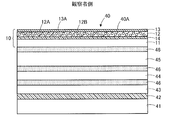
- FIG. 1 is a schematic configuration view of an optical film according to this embodiment
- FIG. 2 is an enlarged view of a part of the optical film shown in FIG. 1
- FIG. 3 is a view schematically showing a state of a folding test. It is.
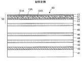
- An optical film 10 shown in FIG. 1 includes a light transmitting substrate 11, a hard coat layer 12, and an inorganic layer 13 in this order.
- the hard coat layer 12 is in contact with the inorganic layer 13.
- the optical film 10 further includes a functional layer 14 between the light transmitting substrate 11 and the hard coat layer 12.
- the optical film 10 shown in FIG. 1 includes the functional layer 14, but the optical film may not include the functional layer.
- the surface 10 ⁇ / b> A of the optical film 10 is a surface 13 ⁇ / b> A of the inorganic layer 13.
- the surface of the optical film is used to mean the surface on one side of the optical film, the surface on the opposite side to the surface of the optical film is the rear surface to distinguish it from the surface of the optical film. It shall be called.
- the back surface 10B of the optical film 10 is a surface on the opposite side to the surface of the light transmitting substrate 11 on the hard coat layer 12 side.
- the haze value (all haze values) of the optical film 10 is preferably 2.5% or less. If the haze value of the optical film 10 is 2.5% or less, excellent transparency can be obtained.
- the haze value is more preferably in the order of 1.5% or less and 1.0% or less (the smaller the numerical value, the more preferable).
- the haze value can be measured by a method based on JIS K7136: 2000 using a haze meter (product name “HM-150”, manufactured by Murakami Color Research Laboratory).
- HM-150 manufactured by Murakami Color Research Laboratory
- the above haze value is cut out to a size of 50 mm ⁇ 100 mm, and then installed so that the inorganic layer side becomes the non-light source side without curling or wrinkles and without fingerprints or dust etc.
- “to measure three times” means to measure three different places instead of measuring the same place three times.
- the visually observed surface 10A is flat, and the layer to be laminated such as the hard coat layer 12 is also flat, and the variation in film thickness is also within the range of ⁇ 10%. Therefore, it is thought that the average value of the haze value of the whole in-plane whole surface of an optical film is obtained by measuring a haze value in three different places of the cut-out optical film. The variation of the haze value is within ⁇ 10% whether the object to be measured is as long as 1 m ⁇ 3000 m or the size of a 5-inch smartphone.
- the optical film can not be cut into the above-mentioned size, for example, since the entrance opening at the time of measurement of HM-150 is 20 mm ⁇ , a sample size having a diameter of 21 mm or more is required. Therefore, the optical film may be cut out to a size of 22 mm ⁇ 22 mm or more.
- the size of the optical film is small, the light source spot is shifted little by little within the range where the light source spot does not go out, or the angle is changed to three measurement points.
- the optical film When the optical film is in the form of a roll, the optical film has an effective part which is a part used for a product (for example, an image display device) and an ineffective part which is a part not used for a product When cutting out an optical film, it shall cut out from the effective part of an optical film. For example, portions up to 5 cm from both ends in the width direction of the optical film may become ineffective portions.
- peeling of other films can be performed, for example, as follows. First, heat the laminate with another film attached to the optical film through the adhesive layer or adhesive layer with a dryer, insert the cutting edge of the cutter in the area that seems to be the interface between the optical film and the other film, and peel slowly I will. By repeating such heating and peeling, the pressure-sensitive adhesive layer, the adhesive layer, and the other films can be peeled off. In addition, even if it has such a peeling process, there is no big influence in the measurement of haze value.
- the total light transmittance of the optical film 10 is preferably 80% or more. If the total light transmittance of the optical film 10 is 80% or more, sufficient light transmittance can be obtained.
- the total light transmittance of the optical film 10 is more preferably in the order of 85% or more and 90% or more (the larger the numerical value, the more preferable).
- the total light transmittance can be measured using a haze meter (product name “HM-150”, manufactured by Murakami Color Research Laboratory) according to a method according to JIS K7361-1: 1997. After cutting out the total light transmittance to a size of 50 mm ⁇ 100 mm, install it so that the inorganic layer side becomes the non-light source side without curling or wrinkles and without fingerprints or dust etc. The measurement is made 3 times, and the measurement is made 3 times to obtain the arithmetic mean value of the values obtained.
- the visually observed surface 10A is flat, and the layer to be laminated such as the hard coat layer 12 is also flat, and the variation in film thickness is also within the range of ⁇ 10%.
- the total light transmittance is measured at three different places of the cut optical film.
- the variation of the total light transmittance is within ⁇ 10% whether the object to be measured is as long as 1 m ⁇ 3000 m or the size of a 5-inch smartphone.
- the size of the optical film is small, the light source spot is shifted little by little within the range where the light source spot does not go out, or the angle is changed to three measurement points.
- the yellow index (YI) of the optical film 10 is preferably 15 or less. If the yellow index YI of the optical film 10 is 15 or less, the yellowness of the optical film is inconspicuous, so that it can be applied to applications where transparency is required.
- the upper limit of the yellow index (YI) of the optical film 10 is more preferably 10 or less.
- the yellow index (YI) is measured on an optical film cut into a size of 50 mm ⁇ 100 mm using a spectrophotometer (product name “UV-3100PC”, manufactured by Shimadzu Corporation, light source: tungsten lamp and deuterium lamp)
- the chromaticity tristimulus values X, Y and Z are calculated from the measured values according to the arithmetic equation described in JIS Z 8722: 2009, and calculated from the tristimulus values X, Y and Z according to the arithmetic equation described in ASTM D1925: 1962. Value.
- the yellow index (YI) is measured three times for one optical film and taken as an arithmetic mean value of values obtained by measuring three times.
- the other film is together with the adhesion layer and the adhesion layer by the same method as described above.
- the yellow index (YI) should be measured after peeling off. In addition, even if there is such a peeling step, the measurement of the yellow index (YI) is not significantly affected.
- the light transmitting substrate 11 or the hard coat layer 12 may contain a blue dye that is a complementary color of yellow.
- a blue dye that is a complementary color of yellow.
- the blue dye may be either a pigment or a dye, but for example, when the optical film 10 is used in an organic light emitting diode display device, one having both light resistance and heat resistance is preferable.
- a pigment or a dye for example, when the optical film 10 is used in an organic light emitting diode display device, one having both light resistance and heat resistance is preferable.
- polycyclic organic pigments, metal complex organic pigments, etc. have a lower degree of molecular breakage due to ultraviolet rays than the molecular dispersion of dyes, and are extremely excellent in light resistance, and therefore applications requiring light resistance etc.
- phthalocyanine-based organic pigments and the like are preferably mentioned.
- the pigment is dispersed in particles in the solvent, and thus the transparency is inhibited due to particle scattering, it is preferable to put the particle size of the pigment dispersion in the Rayleigh scattering region.
- the transparency of the optical film is regarded as important, it is preferable to use a dye which is molecularly dispersed in a solvent as the blue dye.
- the transmittance of light with a wavelength of 380 nm of the optical film 10 is preferably 8% or less.
- the polarizer can be prevented from being exposed to ultraviolet light and deteriorating.
- the upper limit of the transmittance of the optical film 10 is more preferably 5%.
- the transmittance can be measured using a spectrophotometer (trade name “UV-3100PC”, manufactured by Shimadzu Corporation, light source: tungsten lamp and deuterium lamp).
- permeability is measured 3 times with respect to the optical film cut out to the magnitude
- permeability of the optical film 10 can be achieved by adjusting the addition amount of the ultraviolet absorber mentioned later in the hard-coat layer 12, etc.
- the optical film 10 does not break or break in the optical film 10 even if the folding test described below is repeated 100,000 times, and the folding test is performed. It is more preferable that cracking or breakage does not occur in the optical film 10 even in the case of repeating 200,000 times repeatedly, and that cracking or breakage does not occur in the optical film even when repeated repeatedly 1,000,000 times. Is more preferred. In the case where the optical film 10 is repeatedly subjected to the folding test 100,000 times, if the optical film 10 is cracked or the like, the foldability of the optical film 10 becomes insufficient.
- the folding test of the optical film is carried out by the same method as described above. And after peeling off the other film together with the adhesive layer.
- the folding test is performed as follows. As shown in FIG. 3A, in the folding test, first, the side portion 10C of the optical film 10 cut into a size of 20 mm ⁇ 100 mm and the side portion 10D facing the side portion 10C are arranged in parallel. It fixes with the fixed part 20, respectively. In addition, when an optical film can not be cut out in the said magnitude
- the fixing portions 20 are moved close to each other to deform the optical film 10 so as to be folded, and further, as shown in FIG. 3 (C), the optical After moving the fixing portion 20 to a position where the distance between the two opposing side portions 10C and 10D fixed by the fixing portion 20 of the film 10 is 6 mm, the fixing portion 20 is moved in the reverse direction. Eliminate the deformation.
- the optical film 10 can be folded by 180 ° by moving the fixing portion 20 as shown in FIGS. 3 (A) to 3 (C).
- a folding test is performed so that the bent portion 10E of the optical film 10 does not protrude from the lower end of the fixed portion 20, and the distance when the fixed portion 20 approaches closest is controlled by a spacer or the like.
- the distance between the two opposing sides can be 6 mm.
- the outer diameter of the bending portion 10E is considered to be 6 mm.
- the surface 10A of the optical film 10 preferably has a hardness (pencil hardness) of 2H or more when measured by a pencil hardness test defined in JIS K5600-5-4: 1999.
- the pencil hardness test is performed on a surface of an optical film cut into a size of 50 mm ⁇ 100 mm.
- Pencil hardness tester product name “pencil scratch film hardness tester (electric type)” manufactured by Toyo Seiki Co., Ltd.
- Using a pencil product name “Uni”, manufactured by Mitsubishi Pencil Co., Ltd.
- a load of 750 g to move the pencil at a moving speed of 1 mm / sec.
- the pencil hardness is taken as the highest hardness at which the surface of the optical film is not scratched in the pencil hardness test.
- a pencil hardness test is performed 5 times per 1 pencil, and the surface of the optical film may be scratched 4 times or more out of 5 times If not, it is judged that the surface of the optical film was not damaged in the pencil of this hardness.
- the said flaw points out what is visually recognized by having carried out the transmission observation of the surface of the optical film which performed the pencil hardness test under a fluorescent lamp.
- the pencil hardness of the surface 10A of the optical film 10 is more preferably 3H or more, further preferably 5H, and most preferably 6H or more.
- light emitting diodes Light Emitting Diodes
- the light emitting diodes strongly emit light called blue light.
- This blue light has the property of being close to ultraviolet light with a wavelength of 380 to 495 nm, and has strong energy, so it reaches the retina without being absorbed by the cornea or lens, causing damage to the retina or eye It is said to cause mental fatigue and adverse effects on sleep.
- an optical film is applied to an image display apparatus, it is preferable to become a thing excellent in blue light shielding property, without affecting the color of a display screen.
- the optical film 10 has a spectral transmittance of less than 1% at a wavelength of 380 nm, a spectral transmittance of less than 10% at a wavelength of 410 nm, and a spectral transmittance of 70% at a wavelength of 440 nm. % Or more is preferable. If the spectral transmittance at a wavelength of 380 nm is 1% or more, or the spectral transmittance at a wavelength of 410 nm is 10% or more, the problem with blue light may not be resolved, and the spectral transmittance at a wavelength of 440 nm is 70%.
- the optical film 10 sufficiently absorbs light of a wavelength range of 410 nm or less among the blue light wavelengths, while sufficiently transmitting light of a wavelength of 440 nm or more without affecting the color tone of the display screen.
- the shielding properties of the blue light can be made excellent.
- the optical film 10 which is excellent in the shielding property of such blue light is applied to an organic light emitting diode (OLED) display as an image display, it is effective also in deterioration suppression of an organic light emitting diode element.
- the light transmittance of the optical film 10 is almost 0% up to a wavelength of 380 nm, the transmission of light gradually increases from a wavelength of 410 nm, and the transmission of light rapidly increases around a wavelength of 440 nm.
- the spectral transmittance changes so as to draw a sigmoidal curve between wavelengths 410 nm and 440 nm.
- the spectral transmittance at a wavelength of 380 nm is more preferably less than 0.5%, still more preferably less than 0.2%, and the spectral transmittance at a wavelength of 410 nm is more preferably less than 7%, more preferably less than 5%.
- the spectral transmittance at a wavelength of 440 nm is more preferably 75% or more, still more preferably 80% or more.
- the optical film 10 preferably has a spectral transmittance of less than 50% at a wavelength of 420 nm. By satisfying the relationship of such spectral transmittance, the optical film 10 rapidly improves the transmittance around a wavelength of 440 nm, and the blue light shielding property is extremely excellent without affecting the color of the display screen. You can get
- the spectral transmittance at a wavelength of 380 nm in the optical film 10 is more preferably less than 0.1%, the spectral transmittance at a wavelength of 410 nm is more preferably less than 7%, and the spectral transmittance at a wavelength of 440 nm is 80% or more It is more preferable that
- the slope of the transmission spectrum in the wavelength range of 415 to 435 nm obtained using the least squares method is larger than 2.0. If the inclination is 2.0 or less, light may not be cut sufficiently in the blue light light wavelength region, for example, a wavelength range of 415 to 435 nm, and the blue light cut effect may be weakened. In addition, there is also a possibility that the light wavelength range (wavelength 415 to 435 nm) of blue light is cut too much, in which case the backlight of the image display device or the emission wavelength range (for example, light emission from OLED 430 nm) And there is a possibility that problems such as deterioration of color may occur.
- the inclination can be measured, for example, using a spectrophotometer (product name “UV-3100PC”, manufactured by Shimadzu Corporation), which can be measured in 0.5 nm steps, and the data of transmittance for at least 5 points between 1 nm before and after Can be calculated by measuring between 415 and 435 nm.
- a spectrophotometer product name “UV-3100PC”, manufactured by Shimadzu Corporation
- the optical film 10 preferably has a blue light shielding rate of 40% or more. If the blue light shielding rate is less than 40%, the problems caused by the above-described blue light may not be sufficiently solved.
- the shielding rate of the blue light is, for example, a value calculated according to JIS T7333: 2005. Note that such a blue light shielding rate can be achieved, for example, by the hard coat layer 12 containing a sesamol-type benzotriazole-based monomer described later.
- the application of the optical film 10 is not particularly limited, but as the application of the optical film 10, for example, an image display apparatus such as a smartphone, a tablet terminal, a personal computer (PC), a wearable terminal, digital signage, television, car navigation, etc. It can be mentioned.
- the optical film 10 is also suitable for in-vehicle use.
- the form of each of the above-mentioned image display devices is preferable also for applications requiring flexibility such as foldable and rollable.
- the optical film 10 may be cut into a desired size, but may be rolled.
- the size of the optical film is not particularly limited, and is appropriately determined according to the size of the display surface of the image display device.
- the size of the optical film 10 may be, for example, 2.8 inches or more and 500 inches or less.
- "inch” means the length of a diagonal when the optical film has a square shape, means the diameter when the optical film has a circular shape, and the minor axis when it has an elliptical shape. It means the average value of the sum of the major diameter and the major diameter.
- the aspect ratio of the optical film at the time of obtaining the above-mentioned inch is not particularly limited as long as there is no problem as the display screen of the image display device.
- vertical: horizontal 1: 1, 4: 3, 16:10, 16: 9, 2: 1 and the like can be mentioned.
- the size of the optical film 10 is large, after cutting out to A5 size (148 mm x 210 mm) from arbitrary positions, it shall cut out to the size of each measurement item.
- the location of the optical film 10 in the image display device may be inside the image display device, but is preferably near the surface of the image display device.
- the optical film 10 When used near the surface of the image display device, the optical film 10 functions as a cover film used instead of a cover glass.
- the light transmitting substrate 11 is a light transmitting substrate.
- the term "light transmitting” as used herein means the property of transmitting light, and for example, the total light transmittance is 50% or more, preferably 70% or more, more preferably 80% or more, particularly preferably 90%. Including the above.
- the light transmissive property does not necessarily have to be transparent and may be translucent.
- the thickness of the light transmitting substrate 11 is preferably 10 ⁇ m to 100 ⁇ m.
- the thickness of the light transmitting substrate is 10 ⁇ m or more, the curling of the optical film 10 can be suppressed, the hardness is also sufficient, the pencil hardness can be 3H or more, and the optical film is manufactured by Roll to Roll. Since the occurrence of wrinkles can be suppressed, there is no risk of deterioration in the appearance.
- the thickness of the light transmitting substrate 11 is 100 ⁇ m or less, the folding performance of the optical film is sufficient, and it is preferable in terms of weight reduction.
- the thickness of the light transmitting substrate is obtained by photographing a cross section of the light transmitting substrate using a scanning electron microscope (SEM) and measuring the thickness of the light transmitting substrate at 10 points in the image of the cross section Arithmetic mean value of thickness of 10 places.
- the lower limit of the light transmitting substrate 11 is more preferably 25 ⁇ m or more, and the upper limit of the light transmitting substrate 11 is more preferably 80 ⁇ m or less.
- Examples of the constituent material of the light transmitting substrate 11 include resins such as polyimide resins, polyamideimide resins, polyamide resins, and polyester resins (for example, polyethylene terephthalate and polyethylene naphthalate). Among these, not only cracking or breakage is less likely to occur in the folding test, but also excellent hardness and transparency, and also excellent in heat resistance, and by baking, further excellent hardness and transparency can be obtained. From the viewpoint of being able to be applied, a polyimide resin, a polyamide resin, or a mixture thereof is preferable.
- the polyimide resin is obtained by reacting a tetracarboxylic acid component and a diamine component.
- the polyimide-based resin is not particularly limited, but, for example, is selected from the group consisting of the structures represented by the following general formula (1) and the following general formula (3), from the viewpoint of having excellent light transmittance and excellent rigidity. It is preferable to have at least one type of structure.
- R 1 is a tetravalent group which is a tetracarboxylic acid residue
- R 2 is a trans-cyclohexanediamine residue, trans-1,4-bismethylenecyclohexanediamine residue
- 4,4 At least one divalent group selected from the group consisting of a '-diaminodiphenyl sulfone residue, a 3,4'-diaminodiphenyl sulfone residue, and a divalent group represented by the following general formula (2) .
- n represents the number of repeating units and is 1 or more.
- tetracarboxylic acid residue refers to a residue obtained by removing four carboxyl groups from a tetracarboxylic acid
- a residue obtained by removing an acid dianhydride structure from a tetracarboxylic acid dianhydride Represents the same structure.
- a "diamine residue” means the residue remove
- R 3 and R 4 each independently represent a hydrogen atom, an alkyl group or a perfluoroalkyl group.
- R 5 is a cyclohexanetetracarboxylic acid residue, a cyclopentanetetracarboxylic acid residue, a dicyclohexane-3,4,3 ′, 4′-tetracarboxylic acid residue, and 4,4 ′ At least one tetravalent group selected from the group consisting of-(hexafluoroisopropylidene) diphthalic acid residues, and R 6 represents a divalent group which is a diamine residue.
- n ' represents the number of repeating units and is 1 or more.
- R 1 in the above general formula (1) is a tetracarboxylic acid residue, which can be a residue obtained by removing the acid dianhydride structure from the tetracarboxylic acid dianhydride as exemplified above.
- R 1 in the above general formula (1) among them, from the viewpoint of improving light transmittance and rigidity, 4,4 ′-(hexafluoroisopropylidene) diphthalic acid residue, 3,3 ′, 4,4'-biphenyltetracarboxylic acid residue, pyromellitic acid residue, 2,3 ', 3,4'-biphenyltetracarboxylic acid residue, 3,3', 4,4'-benzophenonetetracarboxylic acid residue Selected from the group consisting of a group, 3,3 ', 4,4'-diphenyl sulfone tetracarboxylic acid residue, 4,4'-oxydiphthalic acid residue, cyclohexane te
- the total content of these suitable residues is preferably 50 mol% or more, more preferably 70 mol% or more, and still more preferably 90 mol% or more.
- R 1 is a group consisting of 3,3 ′, 4,4′-biphenyltetracarboxylic acid residue, 3,3 ′, 4,4′-benzophenonetetracarboxylic acid residue, and pyromellitic acid residue.
- a group of tetracarboxylic acid residues (group A) suitable for improving rigidity such as at least one selected, and 4,4 '-(hexafluoroisopropylidene) diphthalic acid residue, 2,3' , 3,4'-biphenyl tetracarboxylic acid residue, 3,3 ', 4,4'-diphenyl sulfone tetracarboxylic acid residue, 4,4'-oxydiphthalic acid residue, cyclohexane tetracarboxylic acid residue, and cyclo It is also preferable to use it in combination with a group of tetracarboxylic acid residues (group B) suitable for improving transparency such as at least one selected from the group consisting of pentanetetracarboxylic acid residues.
- the content ratio of the tetracarboxylic acid residue group (group A) suitable for improving the rigidity and the tetracarboxylic acid residue group (group B) suitable for improving the transparency is 0.05 mol of tetracarboxylic acid residue group (group A) suitable for improving the rigidity with respect to 1 mol tetracarboxylic acid residue group (group B) suitable for improving transparency It is preferably 9 mol or more, more preferably 0.1 mol to 5 mol, and still more preferably 0.3 mol to 4 mol.
- R 2 in the above general formula (1) among them, from the viewpoint of improving light transmittance and rigidity, 4,4′-diaminodiphenyl sulfone residue, 3,4′-diaminodiphenyl sulfone residue And at least one divalent group selected from the group consisting of divalent groups represented by the above general formula (2), and further preferably a 4,4′-diaminodiphenyl sulfone residue, 3 , 4′-diaminodiphenyl sulfone residue, and at least one divalent group selected from the group consisting of divalent groups represented by the above general formula (2) in which R 3 and R 4 are perfluoroalkyl groups. Is preferred.
- R 5 in the above general formula (3) among them, from the viewpoint of improving light transmittance and rigidity, 4,4 ′-(hexafluoroisopropylidene) diphthalic acid residue, 3,3 ′, It is preferable to contain 4,4'-diphenyl sulfone tetracarboxylic acid residue and oxydiphthalic acid residue.
- these preferred residues preferably contains more than 50 mol%, preferably it contains more than 70 mol%, it is preferable to include even more than 90 mol%.
- R 6 in the general formula (3) is a diamine residue, which can be a residue obtained by removing two amino groups from the diamine as exemplified above.
- R 6 in the above general formula (3) among them, from the viewpoint of improving light transmittance and rigidity, a 2,2′-bis (trifluoromethyl) benzidine residue, bis [4- (4-) Aminophenoxy) phenyl] sulfone residue, 4,4'-diaminodiphenyl sulfone residue, 2,2-bis [4- (4-aminophenoxy) phenyl] hexafluoropropane residue, bis [4- (3-amino] Phenoxy) phenyl] sulfone residue, 4,4'-diamino-2,2'-bis (trifluoromethyl) diphenyl ether residue, 1,4-bis [4-amino-2- (trifluoromethyl) phenoxy] benzene Residue, 2,2-bis [4-
- the total content of these suitable residues is preferably 50 mol% or more, more preferably 70 mol% or more, and still more preferably 90 mol% or more.
- R 6 a bis [4- (4-aminophenoxy) phenyl] sulfone residue, a 4,4′-diaminobenzanilide residue, an N, N′-bis (4-aminophenyl) terephthalamide residue, Group of diamine residues suitable for improving rigidity such as at least one member selected from the group consisting of paraphenylene diamine residues, metaphenylene diamine residues, and 4,4'-diaminodiphenylmethane residues (group C) and 2,2'-bis (trifluoromethyl) benzidine residue, 4,4'-diaminodiphenyl sulfone residue, 2,2-bis [4- (4-aminophenoxy) phenyl] hexafluoropropane residue Group, bis [4- (3-aminophenoxy) phenyl] sulfone residue, 4,4'-diamino-2,2'-bis (trifluoromethyl)
- the content ratio of the diamine residue group (group C) suitable for improving the rigidity and the diamine residue group (group D) suitable for improving the transparency improves the transparency.
- 0.05 mol or more and 9 mol or less of diamine residue groups (group C) suitable for improving the rigidity with respect to 1 mol of diamine residues group (group D) suitable for The molar ratio is preferably 0.1 to 5 mol, more preferably 0.3 to 4 mol.
- the number n of repeating units in the polyimide may be appropriately selected according to the structure so as to indicate a preferable glass transition temperature described later, and is not particularly limited.
- the average number of repeating units is usually 10 to 2,000, preferably 15 to 1,000.
- the polyimide resin may partially include a polyamide structure.
- the polyamide structure which may be contained include a polyamideimide structure containing a tricarboxylic acid residue such as trimellitic anhydride, and a polyamide structure containing a dicarboxylic acid residue such as terephthalic acid.
- the polyimide resin preferably has a glass transition temperature of 250 ° C. or higher, and more preferably 270 ° C. or higher.
- the glass transition temperature is preferably 400 ° C. or less, more preferably 380 ° C. or less, from the viewpoint of ease of stretching and reduction of the baking temperature.
- n is a repeating unit and represents an integer of 2 or more.
- polyimide-based resins polyimide-based resins or polyamide-based resins having a structure in which intra-molecular or inter-molecular charge transfer is unlikely to occur are preferable because they have excellent transparency.
- (11) polyimide resins having an alicyclic structure such as those of the above formulas (13) to (16).
- fluorinated polyimide resins such as the above formulas (4) to (11) have high heat resistance because they have a fluorinated structure, and heat during the production of polyimide films made of polyimide resins It has excellent transparency because it is not colored by.
- the polyamide resin is a concept including not only aliphatic polyamide but also aromatic polyamide (aramid).
- the polyamide-based resin generally has a skeleton represented by the following formulas (21) and (22), and as the polyamide-based resin, for example, a compound represented by the following formula (23) It can be mentioned.
- n is a repeating unit and represents an integer of 2 or more.
- a commercially available substrate may be used as the base material composed of the polyimide resin or the polyamide resin represented by the above formulas (4) to (20) and (23).
- the base material which consists of the above-mentioned polyimide system resin neoprim made by Mitsubishi Gas Chemical Co., Ltd. etc. is mentioned, for example,
- a commercial item of the base material which consists of the above-mentioned polyamide system resin For example, Miktron etc. are mentioned.
- the base material composed of the polyimide resin or the polyamide resin represented by the above formulas (4) to (20) and (23) one synthesized according to a known method may be used.
- a synthesis method of a polyimide-based resin represented by the above formula (4) is described in JP-A-2009-132091 and specifically, 4,4′-hexa represented by the following formula (24) It can be obtained by reacting fluoropropylidenebisphthalic acid dianhydride (FPA) with 2,2′-bis (trifluoromethyl) -4,4′-diaminobiphenyl (TFDB).
- FPA fluoropropylidenebisphthalic acid dianhydride
- TFDB 2,2′-bis (trifluoromethyl) -4,4′-diaminobiphenyl
- the weight average molecular weight of the polyimide resin or polyamide resin is preferably in the range of 3,000 to 500,000, more preferably in the range of 5,000 to 300,000, and in the range of 10,000 to 200,000. Is more preferred.
- a weight average molecular weight is the polystyrene conversion value measured by gel permeation chromatography (GPC).
- polyimide resins and polyamide resins polyimide resins or polyamide resins having a structure in which intramolecular or intermolecular charge transfer does not easily occur are preferable because they have excellent transparency.
- Fluorinated polyimide resins such as the above formulas (4) to (11), polyimide resins having an alicyclic structure such as the above formulas (13) to (16), and polyamides having halogen groups such as the above formula (23) Resin is mentioned.
- fluorinated polyimide resins such as the above formulas (4) to (11) have high heat resistance because they have a fluorinated structure, and the heat during the production of a substrate made of polyimide resins It has excellent transparency because it is not colored by.
- the light transmitting substrate 11 has hardness measured under the condition of pencil hardness test (load: 1 kg, speed: 1 mm / sec) defined in JIS K5600-5-4: 1999 on the surface 13A of the inorganic layer 13
- a base material comprising a fluorinated polyimide resin represented by the above formulas (4) to (11) or a polyamide resin having a halogen group such as the above formula (23) is used Is preferred.
- a base material made of a polyimide-based resin represented by the above formula (4) because it can impart extremely excellent hardness of 3 H or more to the above pencil hardness.
- polyester resins include resins having at least one of polyethylene terephthalate, polypropylene terephthalate, polybutylene terephthalate, and polyethylene naphthalate as a component.
- the hard coat layer 12 has an indentation hardness (H IT ) of 200 MPa or more.
- the “indentation hardness” in the present specification is a value determined from a load-displacement curve from loading of an indenter to unloading obtained by hardness measurement by nanoindentation method.
- the lower limit of the indentation hardness (H IT ) of the hard coat layer 12 is preferably 200 MPa or more, 500 MPa or more, and 800 MPa or more in this order (the larger the numerical value, the more preferable).
- the upper limit of the indentation hardness of the hard coat layer 12 is preferably in the order of 1500 MPa or less, 1300 MPa or less, and 1100 MPa or less from the viewpoint of suppressing the occurrence of cracks or cracks in the hard coat layer 12 when the optical film 10 is folded. (The smaller the number, the better).
- H IT indentation hardness
- a block is prepared by embedding an optical film cut into 1 mm ⁇ 10 mm with an embedding resin, and from this block, a uniform thickness of 70 nm or more and 100 nm without holes according to a general section manufacturing method. Cut out the following sections. For preparation of the section, “Ultra Microtome EM UC7” (Leica Microsystems Inc.) or the like can be used. Then, the remaining block from which the uniform section without the hole etc. is cut out is used as a measurement sample.
- the Berkovich indenter is formed of the hard coat layer from the interface between the light transmitting base and the hard coat layer in order to avoid the influence of the light transmitting base and the inorganic layer and to avoid the influence of the side edge of the hard coat layer.
- the center is 500 nm away
- the interface between the hard coat layer and the inorganic layer is 500 nm away from the interface of the hard coat layer
- both sides of the hard coat are 500 nm away from the interface of the hard coat layer. It shall be pressed.
- the center of the hard coat layer is separated by 500 nm from the interface between the functional layer and the hard coat layer, and the interface between the hard coat layer and the inorganic layer And 500 nm on the center side of the hard coat layer, and pushed into portions of the hard coat layer 500 nm on the center side of the hard coat layer from both ends of the hard coat layer.
- the indentation hardness (H IT ) is calculated by P max / A p using The contact projected area is a contact projected area in which the indenter tip curvature is corrected by the Oliver-Pharr method using the standard sample fused quartz (5-0098 manufactured by BRUKER).
- the indentation hardness (H IT ) is the arithmetic mean of the values obtained by measuring 10 points. If the measured values include those that deviate by ⁇ 20% or more from the arithmetic mean value, the measured values are excluded and remeasurement is performed.
- the indentation hardness (H IT ) can be adjusted by the type of binder resin 12A described later, the content of the inorganic particles 12B, and the like. (Measurement condition) Loading speed: 20 ⁇ N / sec Holding time: 5 seconds Load unloading speed: 20 ⁇ N / sec Measuring temperature: 25 ° C.
- the film thickness of the hard coat layer 12 is 1 ⁇ m or more. If the film thickness of the hard coat layer 12 is 1 ⁇ m or more, the degree of penetration of the steel wool decreases at the time of the steel wool test, whereby scratching of the surface of the hard coat layer can be suppressed.
- the lower limit of the hard coat layer 12 is more preferably in the order of 2 ⁇ m or more, 3 ⁇ m or more, and 4 ⁇ m or more (the larger the numerical value, the better).
- the upper limit of the hard coat layer 12 is more preferably 10 ⁇ m or less, 9 ⁇ m or less, 8 ⁇ m or less, 7 ⁇ m or less in order from the viewpoint of obtaining sufficient folding performance (smaller values are more preferable).
- the cross section of the hard coat layer is photographed using a scanning transmission electron microscope (STEM) or a transmission electron microscope (TEM), and the film thickness of the hard coat layer in the image of the cross section It measures ten places and makes it the arithmetic mean value of the film thickness of ten places.
- STEM scanning transmission electron microscope
- TEM transmission electron microscope
- the specific cross-sectional photography method is described below.
- a block is prepared by embedding an optical film cut out into 1 mm ⁇ 10 mm with an embedding resin, and a uniform cut with a thickness of 70 nm or more and 100 nm or less is cut out from this block by a general section preparation method. .
- “Ultra Microtome EM UC7” Leica Microsystems Inc. or the like can be used. Then, a uniform section without this hole or the like is used as a measurement sample. Then, a cross-sectional photograph of the measurement sample is taken using a scanning transmission electron microscope (STEM) (product name “S-4800”, manufactured by Hitachi High-Technologies Corporation). When a cross-sectional photograph is taken using the above S-4800, cross-sectional observation is performed with the detector “TE”, the acceleration voltage “30 kV”, and the emission current “10 ⁇ A”. As for the magnification, the focus is adjusted, and the contrast and the brightness are appropriately adjusted at 5000 to 200,000 times while observing whether each layer can be distinguished.
- STEM scanning transmission electron microscope
- the preferable magnification is 10,000 times to 100,000 times, more preferably 10,000 to 50,000 times, and most preferably 25,000 times to 50,000 times.
- the aperture is set to "beam monitor stop 3"
- the objective lens stop is set to "3”
- W. D. May be "8 mm”.
- the staining process is carried out with osmium tetraoxide, ruthenium tetraoxide, phosphotungstic acid, etc., the interface between the organic layers can be easily seen, so the staining process may be performed.
- the contrast of the interface may be difficult to understand when the magnification is high. In that case, low magnification is also observed simultaneously. For example, observation is made at two high and low magnifications, such as 25,000 times and 50,000 times, 50,000 times and 100,000 times, and the above-mentioned arithmetic average value is obtained with both magnifications, and the average value is further determined by the hard coat layer
- the hard coat layer 12 contains a binder resin 12A and inorganic particles 12B.
- the hard coat layer 12 may contain, in addition to the binder resin 12A and the inorganic particles 12B, additives such as an ultraviolet light absorber and a spectral transmittance modifier.
- an area IR from the interface IF of the hard coat layer 12 to the inorganic layer 13 to a depth of 500 nm of the hard coat layer 12 The area ratio of the inorganic particles 12B in some cases may be referred to as “area” is preferably 5% or more and 75% or less. If the area ratio of the inorganic particles in the interface vicinity region IF is 5% or more, the hard coat layer 12 can be made harder because the hard coat layer 12 contains a large amount of the inorganic particles 12B. The adhesion with can be further improved.
- the steel wool test is performed by applying a load from the surface of the inorganic layer, but in order to rub the surface of the inorganic layer with steel wool, the load is applied not only in the thickness direction of the inorganic layer but also in the shear direction . If the area ratio of the inorganic particles 12B in the near interface region IR is 75% or less, the binder resin 12A exists to some extent in the hard coat layer 12 even when a load is applied in the shear direction by the steel wool test. So it is difficult to scratch and scrape. Further, by the presence of the binder resin 12A in the hard coat layer 12 to some extent, the adhesion to the functional layer 14 can be further improved.
- the reason for determining the area ratio of the inorganic region in the region near the interface is that the region near the interface is particularly susceptible to scratches and scraping when the steel wool test is performed.
- the lower limit of the area ratio of the inorganic particles 12B in the near interface region IF is more preferably in the order of 23% or more, 33% or more, and 44% or more (the larger the numerical value, the more preferable).
- the upper limit of the area ratio of the inorganic particles 12B in the near interface region IF is more preferably in the order of 71% or less, 67% or less, and 60% or less (the smaller the numerical value, the more preferable).
- the area ratio of the inorganic particles in the region near the interface is determined as follows. First, a block is prepared by embedding an optical film cut out into 1 mm ⁇ 10 mm with an embedding resin, and from this block, 10 sections having a thickness of 70 nm or more and 100 nm or less and uniform without holes. Cut out. For preparation of the section, “Ultra Microtome EM UC7” (Leica Microsystems Inc.) or the like can be used. Then, ten uniform slices without the holes and the like are used as measurement samples. Next, a cross-sectional photograph of each measurement sample is taken by a transmission electron microscope (TEM) or a scanning transmission electron microscope (STEM). In addition, one cross-sectional photograph shall be taken per measurement sample.
- TEM transmission electron microscope
- STEM scanning transmission electron microscope
- the area of the region near the interface is set to 100%, and the ratio (area ratio) of the area of the inorganic particles to the area of the region near the interface is determined.
- the area ratio of the inorganic particles in the area near the interface is an arithmetic mean value of the area ratio of the inorganic particles obtained from the cross-sectional photographs of the ten sheets in the area near the interface.
- an area ratio of the inorganic particles 12B for example, 10% or more and 300% or less, preferably 10% or more and 200% or less of the inorganic particles 12B relative to the polymerizable compound to be the binder resin 12A after curing. It is preferable to contain it by a ratio (weight ratio).
- the surface of the hard coat layer 12 on the side of the inorganic layer 13 may be treated to expose the inorganic particles 12B by a method of selectively etching the binder resin 12A.
- the adhesion between the hard coat layer 12 and the inorganic layer 13 can be further improved by performing such treatment. However, if this treatment is performed excessively, the surface of the hard coat layer on the side of the inorganic layer becomes rough and the film thickness of the inorganic layer is thin, so the surface shape of the hard coat is reflected on the surface shape of the inorganic layer When the steel wool test is performed, the steel wool may be caught by the unevenness present on the surface of the inorganic layer, and the scratch resistance may be reduced.
- Examples of methods for selectively etching the binder resin include glow discharge treatment, plasma treatment, ion etching treatment, and alkali treatment.
- the binder resin 12A contains at least one of a polymer (cured product) of a polymerizable compound (curable compound) and a thermoplastic resin.
- the polymerizable compound is one having at least one radically polymerizable functional group and at least one cationically polymerizable functional group in the molecule.
- the polymerizable compound having a radically polymerizable functional group is referred to as a radically polymerizable compound
- the polymerizable compound having a cationically polymerizable functional group is referred to as a cationically polymerizable compound.
- ethylenic unsaturated groups such as a (meth) acryloyl group, a vinyl group, an allyl group
- (meth) acryloyl group is a meaning which includes both "acryloyl group” and "methacryloyl group.”
- the cationically polymerizable functional group include a hydroxyl group, a carboxyl group, an isocyanate group, an amino group, a cyclic ether group and a mercapto group.
- the binder resin 12A preferably contains 10% by mass or more of a polymerizable compound having a polymerizable functional group equivalent weight (weight-average molecular weight / number of polymerizable functional groups) of 130 or more. Hardness can be imparted to the hard coat layer 12 by not containing 10% by mass or more of such a polymerizable compound, so even when the steel wool test is performed on the surface 10A of the optical film 10, a scratch is generated. Hard to produce and hard to scrape. Further, the adhesion between the hard coat layer 12 and the functional layer 14 can be further improved.
- polyfunctional (meth) acrylate is preferable.
- the polyfunctional (meth) acrylate include trimethylolpropane tri (meth) acrylate, tripropylene glycol di (meth) acrylate, diethylene glycol di (meth) acrylate, dipropylene glycol di (meth) acrylate and pentaerythritol tri ( Meta) acrylate, pentaerythritol tetra (meth) acrylate, dipentaerythritol hexa (meth) acrylate, 1,6-hexanediol di (meth) acrylate, neopentyl glycol di (meth) acrylate, trimethylolpropane tri (meth) acrylate , Ditrimethylolpropane tetra (meth) acrylate, dipentaerythritol penta (meth) acrylate, tripentaeryth
- pentaerythritol triacrylate PETA
- dipentaerythritol hexaacrylate DPHA
- pentaerythritol tetraacrylate PETTA
- dipentaerythritol pentaacrylate DPPA
- trimethylolpropane tri (meth) acrylate tripentaerythritol octa (meth) acrylate, tetrapentaerythritol deca (meth) acrylate and the like
- (meth) acrylate means acrylate and methacrylate.
- the monofunctional (meth) acrylate monomer may be further included for hardness adjustment, viscosity adjustment of a composition, adhesion improvement, etc.
- examples of the monofunctional (meth) acrylate monomer include hydroxyethyl acrylate (HEA), glycidyl methacrylate, methoxy polyethylene glycol (meth) acrylate, isostearyl (meth) acrylate, 2-acryloyloxyethyl succinate, acryloyl morpholine, N And acryloyloxyethyl hexahydrophthalimide, cyclohexyl acrylate, tetrahydrofuryl acrylate, isobornyl acrylate, phenoxyethyl acrylate, and adamantyl acrylate.
- HOA hydroxyethyl acrylate
- glycidyl methacrylate methoxy polyethylene glycol (meth) acrylate
- the weight average molecular weight of the monomer is preferably less than 1000, and more preferably 200 or more and 800 or less.
- the weight average molecular weight of the polymerizable oligomer is preferably 1,000 or more and 20,000 or less, more preferably 1,000 or more and 10,000 or less, and still more preferably 2,000 or more and 7,000 or less.
- the cationically polymerizable compound is not particularly restricted but includes, for example, epoxy compounds, polyol compounds, isocyanate compounds, melamine compounds, urea compounds and phenol compounds.
- thermoplastic resin for example, styrene resin, (meth) acrylic resin, vinyl acetate resin, vinyl ether resin, halogen containing resin, alicyclic olefin resin, polycarbonate resin, polyester resin, polyamide resin And cellulose derivatives, silicone resins and rubbers or elastomers.
- the inorganic particles 12B are particles mainly composed of an inorganic substance.
- the inorganic particles 12B may contain an organic component, but are preferably made of only an inorganic substance.
- the inorganic particles 12B may be surface-treated with an organic component.
- the inorganic particles 12B are not particularly limited as long as they can improve the hardness, but silica particles are preferable from the viewpoint of obtaining excellent hardness.
- reactive silica particles are preferable.
- the above-mentioned reactive silica particles are silica particles capable of forming a crosslinked structure with the above-mentioned polyfunctional (meth) acrylate, and by including this reactive silica particle, the hardness of the hard coat layer is sufficient. Can be raised.
- the reactive silica particles preferably have a reactive functional group on the surface, and as the reactive functional group, for example, the above-mentioned polymerizable functional group is suitably used.
- the reactive silica particles are not particularly limited, and conventionally known ones can be used, and examples thereof include reactive silica particles described in JP-A No. 2008-165040. Further, as commercial products of the above reactive silica particles, for example, MIBK-SD, MIBK-SDMS, MIBK-SDL, MIBK-SDZL manufactured by Nissan Chemical Industries, Ltd., V8802, V8803 manufactured by JGC Catalysts Chemical Corporation, etc. It can be mentioned.
- the silica particles may be spherical silica particles, but are preferably modified silica particles.
- spherical silica particles means, for example, silica particles such as true spheres and oval spheres, and "deformed silica particles” have a shape having potato-like random unevenness on the surface. It means silica particles.
- the surface area of the irregular silica particles is larger than that of the spherical silica particles, and by containing such irregular silica particles, the contact area with the polyfunctional (meth) acrylate or the like becomes large, and the hard coat is difficult.
- the hardness of the layer can be improved. It can be confirmed by cross-sectional observation of the functional layer by a transmission electron microscope (TEM) or a scanning transmission electron microscope (STEM) whether it is the above-mentioned unusual silica particle.
- TEM transmission electron microscope
- STEM scanning transmission electron microscope
- the average particle diameter of the said silica particle is 8 nm or more and 100 nm or less. If the average particle diameter of the silica particles is 8 nm or more, adhesion to the inorganic layer 13 can be sufficiently obtained, and if 100 nm or less, whitening can be suppressed.
- the upper limit of the average particle size of the silica particles is more preferably in the order of 65 nm or less, 40 nm or less, and 25 nm or less (the smaller the numerical value, the better).
- the average particle size of the silica particles is measured using an image processing software from an image taken with a transmission electron microscope (TEM) or a scanning transmission electron microscope (STEM) It is a value.
- the average particle diameter of the silica particles is the outer periphery of the atypical silica particles that appeared in the image taken with a transmission electron microscope (TEM) or a scanning transmission electron microscope (STEM) The average value of the maximum value (major axis) and the minimum value (minor axis) of the distance between the two points.
- the silica particles may be a mixture of the above-mentioned reactive silica particles and non-reactive silica particles, a mixture of first silica particles and a second silica particle having a particle diameter smaller than that of the first silica particles.
- a mixture of the reactive silica particles and the nonreactive silica particles is used, curling can be suppressed while maintaining the adhesion to the inorganic layer 13 and the scratch resistance.
- the mixture of the said 1st silica particle and 2nd silica particle is used, the hardness of a hard-coat layer can further be improved, and, thereby, abrasion resistance can be improved more.
- Optical films are particularly suitably used for mobile terminals such as flexible smartphones and tablet terminals, but such mobile terminals are often used outdoors, and therefore, they are disposed closer to the display element than the optical films.
- the polarizer is easily deteriorated by being exposed to ultraviolet light.
- the hard coat layer is disposed on the display screen side of the polarizer, when the hard coat layer contains an ultraviolet absorber, the deterioration due to the exposure of the polarizer to ultraviolet rays is suitably prevented. be able to.
- a ultraviolet absorber As a ultraviolet absorber, a triazine type ultraviolet absorber, a benzophenone series ultraviolet absorber, a benzotriazole type ultraviolet absorber etc. are mentioned, for example.
- triazine-based UV absorber examples include 2- (2-hydroxy-4- [1-octyloxycarbonylethoxy] phenyl) -4,6-bis (4-phenylphenyl) -1,3,5-triazine, for example.
- benzophenone-based UV absorbers examples include 2-hydroxybenzophenone, 2,4-dihydroxybenzophenone, 2,2'-dihydroxy-4,4'-dimethoxybenzophenone, 2,2 ', 4,4'-tetrahydroxy Benzophenone, 2-hydroxy-4-methoxybenzophenone, hydroxymethoxybenzophenone sulfonic acid and its trihydrate, sodium hydroxymethoxybenzophenone sulfonate and the like can be mentioned.
- benzophenone-based ultraviolet absorbers examples include CHMASSORB 81 / FL (manufactured by BASF).
- benzotriazole-based UV absorber examples include 2-ethylhexyl-3- [3-tert-butyl-4-hydroxy-5- (5-chloro-2H-benzotriazol-2-yl) phenyl] propionate, and the like.
- benzotriazole-based ultraviolet absorbers examples include KEMISORB 71 D, KEMISORB 79 (all are Chemipro Chemical Co., Ltd. made), JF-80, JAST-500 (all are Johoku Chemical Co., Ltd.), ULS- 1933D (manufactured by Lion Specialty Chemicals Co., Ltd.), RUVA-93 (manufactured by Otsuka Chemical Co., Ltd.), and the like.
- UV absorbers triazine-based UV absorbers and benzotriazole-based UV absorbers are preferably used. It is preferable that the ultraviolet absorber has high solubility with the resin component that constitutes the functional layer, and that the bleed out after the above-described folding test be small.
- the UV absorber is preferably polymerized or oligomerized.
- the UV absorber is preferably a benzotriazole, triazine, a polymer or oligomer having a benzophenone skeleton, and more specifically, a benzotriazole or (meth) acrylate having a benzophenone skeleton and methyl methacrylate (MMA) in any ratio. It is preferable that it is thermally copolymerized.
- the UV absorber can also play a role of protecting the OLED from UV light.
- a ultraviolet absorber Although it does not specifically limit as content of a ultraviolet absorber, It is preferable that they are 1 mass part or more and 6 mass parts or less with respect to 100 mass parts of solid content of the composition for functional layers. If it is less than 1 part by mass, the effect of including the above-mentioned ultraviolet light absorber in the functional layer may not be sufficiently obtained, and if it exceeds 6 parts by mass, significant coloring and strength reduction may occur in the functional layer. is there.
- the more preferable lower limit of the content of the ultraviolet absorber is 2 parts by mass or more, and the more preferable upper limit is 5 parts by mass or less.
- a spectral transmission factor adjustment agent adjusts the spectral transmission factor of an optical film.
- the hard coat layer 12 contains, for example, a sesamol-type benzotriazole-based monomer represented by the following general formula (21), the above-described spectral transmittance can be suitably satisfied.
- R 7 represents a hydrogen atom or a methyl group.
- R 8 represents a linear or branched alkylene group having 1 to 6 carbon atoms or a linear or branched oxyalkylene group having 1 to 6 carbon atoms.
- the above-mentioned sesamol-type benzotriazole-based monomer is not particularly limited, but specific substance name is 2- [2- (6-hydroxybenzo [1,3] dioxol-5-yl) -2H-benzo Triazol-5-yl] ethyl methacrylate, 2- [2- (6-hydroxybenzo [1,3] dioxol-5-yl) -2H-benzotriazol-5-yl] ethyl acrylate, 3- [2- (6 -Hydroxybenzo [1,3] dioxol-5-yl) -2H-benzotriazol-5-yl] propyl methacrylate, 3- [2- (6-hydroxybenzo [1,3] dioxol-5-yl) -2H -Benzotriazol-5-yl] propyl acrylate, 4- [2- (6-hydroxybenzo [1,3] dioxol-5-yl -2H-benzotriazol-5-yl] butyl me
- the sesamol-type benzotriazole monomer is contained in the hard coat layer 12, for example, the sesamol-type benzotriazole monomer is contained in 15 to 30% by mass in the hard coat layer 12. Is preferred. By containing the sesamol-type benzotriazole-based monomer in such a range, the above-described spectral transmittance can be satisfied.
- the sesamol-type benzotriazole-based monomer may be contained integrally in the hard coat layer 12 by reacting with the resin component constituting the hard coat layer 12, and the resin constituting the hard coat layer 12 You may contain independently, without reacting with a component.
- the inorganic layer 13 is a layer mainly composed of an inorganic substance, and, for example, if the inorganic substance is present in an amount of 55% by mass or more in the inorganic layer, it corresponds to the inorganic layer.
- the inorganic layer 13 may contain an organic component, but is preferably made of only an inorganic substance. Whether or not the layer in contact with the hard coat layer 12 corresponds to an inorganic layer can be confirmed by X-ray photoelectron spectroscopy (XPS) or electron spectroscopy for chemical analysis (ESCA) it can.
- XPS X-ray photoelectron spectroscopy
- ESCA electron spectroscopy for chemical analysis
- the inorganic layer 13 preferably contains silicon.
- the refractive index can be reduced. Whether or not silicon is contained in the inorganic layer can be confirmed by X-ray photoelectron spectroscopy (XPS) or electron spectroscopy for chemical analysis (ESCA).
- XPS X-ray photoelectron spectroscopy
- ESA electron spectroscopy for chemical analysis
- the thickness of the inorganic layer 13 is preferably 10 nm or more and 300 nm or less. If the film thickness of the inorganic layer 13 is 10 nm or more, excellent scratch resistance can be imparted, and if 300 nm or less, the adhesiveness with other layers is good without affecting the flexibility or the optical properties. It is.
- the lower limit of the film thickness of the inorganic layer 13 is more preferably in the order of 30 nm or more, 50 nm or more, 80 nm or more (more preferably as the numerical value is larger), and the upper limit is more preferably in the order of 250 nm or less, 200 nm or less, 150 nm or less ).
- the film thickness of the inorganic layer 13 is determined by the same method as the film thickness of the hard coat layer 12.
- the water vapor transmission rate (WVTR: Water Vapor Transmission Rate) at 40 ° and a relative humidity of 90% is preferably 100 g / (m 2 ⁇ 24 h) or less. Fold resistance is worse at higher temperatures and higher relative humidity. It is considered that this is because the inorganic layer 13 permeates moisture, and the permeated moisture causes hydrolysis of the hard coat layer.
- the water vapor transmission rate of the inorganic layer 13 is 100 g / (m 2 ⁇ 24 h) or less, the moisture passing through the inorganic layer 13 can be reduced, so that the hydrolysis of the hard coat layer can be suppressed. it can.
- the water vapor transmission rate is a numerical value obtained by the method according to JIS K7129: 2008.
- the water vapor transmission rate can be measured using a water vapor transmission rate measuring device (product name "PERMATRAN-W3 / 31", manufactured by MOCON).
- the water vapor transmission rate is an average of the values obtained by measuring three times.
- the inorganic layer 13 can be formed, for example, using a vapor deposition method such as a PVD method or a CVD method.
- a vapor deposition method such as a PVD method or a CVD method.
- a vacuum evaporation method a vacuum evaporation method, sputtering method, ion plating method etc. are mentioned, for example.
- a vacuum evaporation method the vacuum evaporation method by an electron beam (EB) heating system, the vacuum evaporation method by a high frequency dielectric heating system, etc. are mentioned, for example.
- EB electron beam
- the functional layer 14 is a layer that exerts some function in the optical film 10, and examples of the functional layer 14 include an optical adjustment layer, an antistatic layer, and the like.
- the function exhibited by the functional layer 14 may be two or more.
- the functional layer 14 may be a layer that exhibits both the optical adjustment function and the antistatic function.
- the film thickness of the functional layer 14 is preferably 30 nm or more and 200 nm or less. If the film thickness of the functional layer 14 is 30 nm or more, sufficient adhesion between the hard coat layer 12 and the optical adjustment layer 14 can be secured, and if 200 nm or less, interference fringes can be further suppressed.
- the lower limit of the functional layer 14 is more preferably in the order of 50 nm or more, 70 nm or more, 90 nm or more (more preferably as the numerical value is larger), and the upper limit is more preferably in the order of 150 nm or less, 140 nm or less, 130 nm or less (preferably as the numerical value is smaller).
- the film thickness of the functional layer 14 is determined by the same method as the film thickness of the hard coat layer 12.
- the optical adjustment layer is a layer for suppressing the occurrence of interference fringes.
- the refractive index of the optical adjustment layer is preferably lower than the refractive index of the light transmitting substrate 11 and higher than the refractive index of the hard coat layer 12 from the viewpoint of suppressing the generation of interference fringes.
- the refractive index of the optical adjustment layer can be measured, for example, by the Becke method.
- the refractive index of the optical adjustment layer In the case of measuring the refractive index of the optical adjustment layer using the Becke method, ten pieces of the optical adjustment layer are cut out, and in the 10 pieces cut out, the refractive index is measured by the Becke method using a refractive index standard solution The average of ten measured refractive indices of the measured fragments is taken as the refractive index of the optical adjustment layer.
- the refractive index of the light transmitting substrate 11 or the hard coat layer 12 can also be measured by the same method as the refractive index of the optical adjustment layer.
- the difference in refractive index between the optical adjustment layer and the hard coat layer 12 is preferably 0.005 or more and 0.100 or less. If this refractive index difference is 0.005 or more, interface reflection between the optical adjustment layer and the hard coat layer 12 occurs but the interference fringes can not be visually recognized, and if it is 0.100 or less, interference is caused. Although the streaks are slightly confirmed, they can be made at a level that causes no problem in practical use.
- the lower limit of the refractive index difference is more preferably 0.007 or more, and the upper limit is more preferably 0.090 or less.
- the refractive index of the optical adjustment layer may be 0.010 or more and 0.080 or less.
- the optical adjustment layer may be made of only a resin, but preferably contains a binder resin and particles for adjusting the refractive index.
- the optical adjustment layer may further contain an antistatic agent in order to exert an antistatic function.
- the binder resin of the optical adjustment layer is selected from the group consisting of (meth) acrylic resin, cellulose resin, urethane resin, vinyl chloride resin, polyester resin, polyolefin resin, polycarbonate, nylon, polystyrene, and ABS resin.
- the particles of the optical adjustment layer 14 are at least one selected from the group consisting of low refractive index particles such as silica and magnesium fluoride, metal oxide particles such as titanium oxide and zirconium oxide, and inorganic pigments such as cobalt blue. Is preferred. Among these, a combination of a polyester resin and metal oxide particles such as titanium oxide or zirconium oxide is more preferable from the viewpoint of adhesion and adjustment of refractive index difference.
- the antistatic layer contains an antistatic agent.
- the antistatic agent there are an ion conductive antistatic agent and an electron conductive antistatic agent, and from the viewpoint of compatibility with the binder resin, an ion conductive antistatic agent is preferable.
- the ion conductive antistatic agent examples include cationic antistatic agents such as quaternary ammonium salts and pyridinium salts, and alkali metal salts such as sulfonic acids, phosphoric acids and carboxylic acids (for example, lithium salts, sodium salts, And anionic antistatic agents such as potassium salts, etc .; amphoteric antistatic agents such as amino acids and amino acid sulfate esters; and nonionic antistatic agents such as amino alcohols, glycerins and polyethylene glycols.
- quaternary ammonium salts and lithium salts are preferable because they exhibit excellent compatibility with the binder resin.
- the electron conductive antistatic agent examples include conductive particles such as polyacetylene-based and polythiophene-based conductive polymers, metal particles, and metal oxide particles.
- conductive particles such as polyacetylene-based and polythiophene-based conductive polymers, metal particles, and metal oxide particles.
- antistatic agents, metal particles and metal oxide particles in which a conductive polymer such as polyacetylene or polythiophene is combined with a dopant are preferable.
- the conductive polymer can also contain conductive particles.
- antistatic agent comprising the above conductive polymer
- examples of the antistatic agent comprising the above conductive polymer include polyacetylene, polyaniline, polythiophene, polypyrrole, polyphenylene sulfide, poly (1,6-heptadiyne), polybiphenylene (polyparaphenylene), polyparafinylene sulfide, Conductive polymers such as polyphenylacetylene, poly (2,5-thienylene), or derivatives thereof are mentioned, and preferably, conductive organic polymers of polythiophene type (for example, 3,4-ethylenedioxythiophene ( PEDOT) and the like.
- PEDOT 3,4-ethylenedioxythiophene
- an antistatic agent comprising the above-mentioned conductive organic polymer
- the humidity dependency is small and the antistatic property can be maintained for a long period of time, and high transparency, low haze value is realized, and further, high hard coatability, In particular, pencil hardness, scratch resistance to steel wool and the like can be remarkably improved.
- the metal constituting the metal particles is not particularly limited, and examples thereof include Au, Ag, Cu, Al, Fe, Ni, Pd, Pt and the like alone or an alloy of these metals.
- the metal oxide constituting the metal oxide particles is not particularly limited. For example, tin oxide (SnO 2 ), antimony oxide (Sb 2 O 5 ), antimony-doped tin oxide (ATO), tin-doped indium oxide (tin oxide) ITO), aluminum-doped zinc oxide (AZO), fluorine-doped tin oxide (FTO), zinc oxide (ZnO) and the like.
- the content of the antistatic agent is not particularly limited, but it is preferably 1 part by mass or more and 50 parts by mass or less with respect to 100 parts by mass of the polymerizable compound of the composition for antistatic layer. If it is 1 part by mass or more, the above-mentioned antistatic property can be sufficiently obtained, and if it is 50 parts by mass or less, a highly transparent film having a small haze value and a good total light transmittance can be obtained.
- the lower limit of the content of the antistatic agent is more preferably 10 parts by mass or more, and the upper limit is more preferably 40 parts by mass or less.
- the optical film 10 can be produced, for example, as follows. First, a composition for functional layer for forming the functional layer 14 is applied on one surface of the light transmitting substrate 11 by a coating apparatus such as a bar coater, and a coating film of the composition for functional layer is obtained. Form.
- the composition for functional layers here is a composition for optical adjustment layers, the composition for antistatic layers may be sufficient.
- the composition for a functional layer contains particles of a binder resin precursor, a metal oxide or the like and a solvent.
- the composition for a functional layer may further contain, if necessary, at least one of low refractive index particles such as silica and magnesium fluoride, inorganic pigments such as cobalt blue, a leveling agent, and a polymerization initiator.
- the composition for the functional layer may additionally contain, if necessary, (meth) acrylic resin, cellulose resin, urethane resin, and vinyl chloride resin. It may contain one or more resins selected from the group consisting of resins, polyolefin resins, polycarbonates, nylons, polystyrenes, and ABS resins.
- the coating film After forming a coating film of the composition for a functional layer, the coating film is dried by heating for 10 seconds to 120 seconds at a temperature of 40 ° C. or more and 200 ° C. or less by various known methods, for example, to evaporate the solvent.
- the functional layer 14 is formed by curing or, if necessary, irradiating the coating film with ionizing radiation such as ultraviolet light.
- the composition for hard coat layer for forming the hard coat layer 12 is applied on the functional layer 14 by a coating apparatus such as a bar coater, and the composition for the hard coat layer is coated Form a film.
- composition for hard coat layer contains a polymerizable compound that becomes the binder resin 12A after curing and the inorganic particles 12B.
- the composition for hard coat layer may further contain, if necessary, an ultraviolet light absorber, a spectral transmittance regulator, a leveling agent, a solvent, and a polymerization initiator.
- solvent examples include alcohols (eg, methanol, ethanol, propanol, isopropanol, n-butanol, s-butanol, t-butanol, benzyl alcohol, PGME, ethylene glycol, diacetone alcohol), ketones (eg, acetone, methyl ethyl ketone, Methyl isobutyl ketone, cyclopentanone, cyclohexanone, heptanone, diisobutyl ketone, diethyl ketone, diacetone alcohol, ester (methyl acetate, ethyl acetate, butyl acetate, n-propyl acetate, isopropyl acetate, methyl formate, PGMEA), aliphatic Hydrocarbons (eg, hexane, cyclohexane), halogenated hydrocarbons (eg, methylene chloride, chloroform,
- alcohols
- solvents may be used alone or in combination of two or more.
- methyl isobutyl ketone and methyl ethyl ketone are preferred as the solvent, since components such as urethane (meth) acrylate and other additives can be dissolved or dispersed and the composition for the resin layer can be suitably coated. preferable.
- the polymerization initiator is a component that is decomposed by ionizing radiation or heat to generate radicals to initiate or promote polymerization (crosslinking) of the polymerizable compound.
- the polymerization initiator is not particularly limited as long as it can release a substance that initiates radical polymerization by ionizing radiation or heat.
- the polymerization initiator is not particularly limited, and known ones may be used. Specific examples thereof include, for example, acetophenones, benzophenones, Michler's benzoylbenzoate, ⁇ -amyloxime ester, thioxanthones, propiophenone , Benzyls, benzoins, acyl phosphine oxides. Also, it is preferable to use a mixture of photosensitizers, and specific examples thereof include n-butylamine, triethylamine, poly-n-butylphosphine and the like.
- the coating film After forming a coating film of the composition for a hard coat layer, the coating film is dried by heating at a temperature of 30 ° C. or more and 120 ° C. or less for 10 seconds to 120 seconds by various known methods to evaporate the solvent. .
- the coated film is dried, the coated film is irradiated with ionizing radiation such as ultraviolet light to cure the coated film, thereby forming the hard coat layer 12.
- ionizing radiation such as ultraviolet light
- the inorganic layer 13 is formed in contact with the hard coat layer 12 by, for example, a vapor deposition method such as a sputtering method. Thereby, the optical film 10 shown in FIG. 1 is obtained.
- FIG. 4 is a schematic block diagram of the image display apparatus according to the present embodiment. As shown in FIG. 4, the image display device 40 is mainly directed to the observer side, and a housing 41 in which a battery or the like is accommodated, a protective film 42, a display panel 43, a touch sensor 44, and a circularly polarizing plate 45. , And the optical film 10 are laminated in this order.
- An adhesive layer 46 is disposed, and the members are fixed to each other by a light transmitting adhesive layer 46.
- the optical film 10 is disposed such that the hard coat layer 12 is closer to the viewer than the light transmitting substrate 11.
- the surface 10A of the optical film 10 constitutes the surface 40A of the image display device 40.
- the display panel 43 is an organic light emitting diode panel including an organic light emitting diode and the like.
- the touch sensor 44 is disposed closer to the display panel 43 than the circularly polarizing plate 45, but may be disposed between the circularly polarizing plate 45 and the optical film 10. Further, the touch sensor 44 may be an on-cell system or an in-cell system.
- the inventors of the present invention conducted intensive studies on the scratch resistance of the optical film in which the inorganic layer was formed on the hard coat layer, and contained inorganic particles in the hard coat layer to make the thickness of the hard coat layer It was found that the abrasion resistance can be improved by setting it to 1 ⁇ m or more and setting the indentation hardness of the hard coat layer to 200 MPa or more. It is considered that this is because adhesion to the inorganic layer was secured and high hardness of the hard coat layer was achieved by blending appropriate inorganic particles in the appropriate hard coat layer.
- the film thickness of the hard coat layer 12 including the binder resin 12A and the inorganic particles 12B is 1 ⁇ m or more, and the indentation hardness of the hard coat layer 12 is 200 MPa or more.
- An optical film 10 can be provided.
- the hard coat layer does not contain the inorganic particles from the viewpoint of improving the scratch resistance, but in the present embodiment, the inorganic layer 13 is formed on the hard coat layer 12 Therefore, the inorganic particles 12B in the hard coat layer 12 can be suppressed from falling off during the steel wool test. Thereby, the hardness of the hard-coat layer 12 can be raised by containing the inorganic particle 12, and abrasion resistance can be improved.
- FIG. 5 is a schematic configuration view of an optical film according to the present embodiment.
- members denoted with the same reference numerals as those in FIG. 1 are the same as the members shown in FIG.
- the optical film 50 shown in FIG. 5 includes the light transmitting substrate 11, the hard coat layer 51, and the inorganic layer 13 in this order.
- the surface 50A of the optical film 50 is the surface 13A of the inorganic layer 13
- the back surface 50B is the surface of the light transmitting substrate 11 opposite to the surface on the hard coat layer 51 side. ing. Since the physical properties of the optical film 50 are the same as the physical properties of the optical film 10, the description is omitted here.
- the hard coat layer 51 has an indentation hardness of 200 MPa or more and a thickness of 1 ⁇ m or more for the same reason as the reason described in the section of the hard coat layer 12.
- the preferred upper and lower limits of the indentation hardness and film thickness of the hard coat layer 51 are the same as the preferred upper and lower limits of the indentation hardness and film thickness of the hard coat layer 12.
- the other physical properties and the like of the hard coat layer 51 are the same as the physical properties and the like of the hard coat layer 12, and therefore the description thereof is omitted here.
- the hard coat layer 51 contains at least one of a metal element and a metalloid element.
- the adhesion to the inorganic layer 13 can be improved, so that the abrasion resistance can be improved.
- the metal element may be, for example, a typical metal element such as aluminum or tin or a transition metal element such as zirconium or titanium.
- examples of the metalloid element include boron, silicon, germanium, arsenic, antimony and tellurium. Whether or not the hard coat layer contains the above-mentioned elements can be confirmed by the following method.
- the film thickness of the inorganic layer is greater than that of the inorganic layer with a microtome (product name “Ultra Microtome EM UC7”, manufactured by Leica Microsystems Inc.) at an angle of 2 ° or less Cut to expose the hard coat layer.
- elemental analysis is performed from the surface obtained by the above-mentioned cutting using an X-ray photoelectron spectrometer (ESCA, product name "KRATOS Nova", manufactured by Shimadzu Corporation). This makes it possible to confirm whether the hard coat layer contains at least one of a metal element and a metalloid element.
- the total atomic ratio of the metal element and the metalloid element contained in the hard coat layer 51 and measured by X-ray photoelectron spectroscopy is preferably 1.5% or more and 30% or less. If the atomic ratio of the total of the metal element and the metalloid element is 1.5% or more, adhesion with the inorganic layer 13 can be further improved, and if it is 30% or less, flexibility is obtained. Can be maintained.
- the atomic ratio of the total of the metal element and the metalloid element is an X-ray photoelectron spectrometer (ESCA, product name “KRATOS Nova”, Shimadzu Co., Ltd., on the surface obtained by cutting to perform the above-mentioned elemental analysis. It shall be measured using a manufacturing company).
- the lower limit of the atomic ratio of the total amount of the metal element and the metalloid element in the hard coat layer 51 is more preferably 2% or more and 5% or more (more preferably as the numerical value is larger), the upper limit is 25% In the following, it is more preferable that the content is 20% or less (the smaller the numerical value, the better).
- the hard coat layer 51 preferably contains the silicone resin 51A and the inorganic particles 51B from the viewpoint of further improving the scratch resistance. However, if the hard coat layer 51 contains at least one of a metal element and a metalloid element, both the silicone resin 51A and the inorganic particles 51B may not be contained. For example, when the hard coat layer contains a silicone resin, since the hard coat layer contains silicon derived from a silicone resin, the inorganic particles 51B may not be contained. When the hard coat layer contains silica particles as inorganic particles, the hard coat layer does not need to contain a silicone resin because it contains silicon derived from silica particles.
- the "silicone resin” in the present specification means a polymer compound having a main skeleton by siloxane bond (bond of silicon and oxygen).
- the hard coat layer 51 may contain, in addition to the silicone resin 51A and the inorganic particles 51B, an additive such as an ultraviolet light absorber and a spectral transmittance modifier.
- the silicone resin 51A is preferably a polymer (cured product) of a polymerizable compound containing silsesquioxane represented by the general formula (R 9 SiO 1.5 ) n having a polymerizable functional group.
- R 9 is a polymerizable functional group such as a radically polymerizable functional group or a cationically polymerizable functional group
- n is an integer of 1 or more.
- the polymerizable compound may contain other polymerizable compounds in addition to the above silsesquioxane, but may be only the above silsesquioxane.
- Adhesiveness with the inorganic layer can be further secured by the silicone resin 51A containing a polymer of a polymerizable compound containing such silsesquioxane.
- the radically polymerizable functional group include ethylenic unsaturated groups such as (meth) acryloyl group, vinyl group and allyl group, and the like, and examples of cationically polymerizable functional groups include epoxy group and oxetanyl group. It can be mentioned.
- silsesquioxanes can be linked to each other, and a polymer can be obtained.
- silsesquioxane is not particularly limited, and includes, for example, a cage structure such as a complete cage structure and an incomplete cage structure, a ladder structure, a random structure and the like, but any structure may be used. Good.
- examples of commercially available products of silsesquioxane include Glycidyl polysilsesquioxane cage mixture manufactured by Constour Chemical Co., Ltd. and a photocurable SQ series manufactured by Toagosei Co., Ltd.
- the polymerizable compound forming the silicone resin 51A is dimethylpolysiloxane having a radically polymerizable functional group such as (meth) acryloyl group, silicone oligomer having an alkoxysilyl group, and / or silicone instead of the above silsesquioxane. It may contain a polymer or the like.
- the above-mentioned silicone oligomer or silicone polymer preferably has a polymerizable functional group such as a radically polymerizable functional group or a cationically polymerizable functional group from the viewpoint of being able to further increase the hardness of the hard coat layer.
- dimethylpolysiloxanes having a radically polymerizable functional group include KR series manufactured by Shin-Etsu Chemical Co., Ltd., for example, KP-410, KP-411, KP-412, KP-413, KP-414, KP- 415, KP-423 (both ends), KP-416, KP418, KP-422 (all ends), and KP-420 (side chains).
- silicone oligomers having an alkoxysilyl group examples include KR-500, KR-515, KC-895, X-40-9225, etc. manufactured by Shin-Etsu Chemical Co., Ltd. Further, as the ultrahigh molecular weight silicone resin, for example, KR-251 manufactured by Shin-Etsu Chemical Co., Ltd. and the like can be mentioned.
- the inorganic particles 51B are the same as the inorganic particles 12B described in the first embodiment, and thus the description thereof is omitted here.
- the inventors of the present invention conducted intensive studies on the scratch resistance of an optical film having an inorganic layer formed on a hard coat layer, and found that the hard coat layer contains at least one of a metal element and a metalloid element. It has been found that the scratch resistance can be improved by setting the film thickness of the hard coat layer to 1 ⁇ m or more and the indentation hardness of the hard coat layer to 200 MPa or more. This is considered to be because adhesion to the inorganic layer was secured and high hardness of the hard coat layer was achieved by including at least one of the metal element and the metalloid element in the hard coat layer. .
- the film thickness of the hard coat layer 51 containing at least one of a metal element and a metalloid element is 1 ⁇ m or more, and the indentation hardness of the hard coat layer 51 is 200 MPa or more.
- An optical film 50 having scratch resistance can be provided.
- the hard coat layer does not contain inorganic particles from the viewpoint of improving the scratch resistance, but in the present embodiment, the inorganic layer 13 is formed on the hard coat layer 51. Therefore, the inorganic particles 51B in the hard coat layer 51 can be prevented from falling off during the steel wool test. Thereby, the hardness of the hard-coat layer 51 can be raised by containing the inorganic particle 51B, and abrasion resistance can be improved.
- FIG. 6 is a schematic block diagram of an image display device according to the present embodiment.
- An image display device 60 shown in FIG. 6 includes an optical film 50.
- the image display device 60 is the same as the image display device 40 except that the optical film 10 is used as the optical film 50, and thus the description thereof is omitted here.
- solid content 100% conversion value is a value when solid content in solvent dilution goods is made into 100%.
- composition for hard coat layer 1 -Polyester acrylate (product name "M-9050", manufactured by Toagosei Co., Ltd.): 50 parts by mass-Silica particles (product name "MIBK-SD”, manufactured by Nissan Chemical Industries, Ltd.): 50 parts by mass-Polymerization initiator ( 1-hydroxycyclohexyl phenyl ketone, product name "Irgacure (registered trademark) 184", manufactured by BASF Japan Ltd.): 5 parts by mass, methyl isobutyl ketone: 100 parts by mass
- composition for hard coat layer 2 -Polyester acrylate (product name "M-9050", manufactured by Toagosei Co., Ltd.): 67 parts by mass-Silica particles (product name "MIBK-SD”, manufactured by Nissan Chemical Industries, Ltd.): 33 parts by mass-Polymerization initiator ( 1-hydroxycyclohexyl phenyl ketone, product name "Irgacure (registered trademark) 184", manufactured by BASF Japan Ltd.): 5 parts by mass, methyl isobutyl ketone: 100 parts by mass
- composition for hard coat layer 3 -Polyester acrylate (product name "M-9050”, manufactured by Toagosei Co., Ltd.): 90 parts by mass-Silica particles (product name "MIBK-SD”, manufactured by Nissan Chemical Industries, Ltd.): 10 parts by mass-Polymerization initiator ( 1-hydroxycyclohexyl phenyl ketone, product name "Irgacure (registered trademark) 184", manufactured by BASF Japan Ltd.): 5 parts by mass, methyl isobutyl ketone: 100 parts by mass
- composition for hard coat layer 4 -Alkoxylated dipentaerythritol acrylate (product name "A-DPH-12E", manufactured by Shin-Nakamura Chemical Co., Ltd.): 50 parts by mass-Silica particles (product name "MIBK-SD”, manufactured by Nissan Chemical Industries, Ltd.): 50 parts by weight of a polymerization initiator (1-hydroxycyclohexyl phenyl ketone, product name “Irgacure® 184”, manufactured by BASF Japan Ltd.): 5 parts by weight of methyl isobutyl ketone: 100 parts by weight
- composition for hard coat layer 5 -Glycidyl polysilsesquioxane (product name "Glycidyl polysilsesquioxane cage mixture", manufactured by Constour Chemical Co., Ltd.): 100 parts by mass-Polymerization initiator (tri-p-tolyl sulfonium hexafluorophosphate, manufactured by Tokyo Chemical Industry Co., Ltd. ): 5 parts by mass 1-methoxy-2-propanol: 100 parts by mass
- composition 6 for hard coat layer -Polyester acrylate (product name "M-9050”, manufactured by Toagosei Co., Ltd.): 100 parts by mass-Polymerization initiator (1-hydroxycyclohexyl phenyl ketone, product name "Irgacure (registered trademark) 184", manufactured by BASF Japan Ltd.) 5 parts by mass methyl isobutyl ketone 100 parts by mass
- composition 7 for hard coat layer Polypropylene glycol diacrylate (product name "M-220", manufactured by Toagosei Co., Ltd.): 90 parts by mass-Silica particles (product name "MIBK-SD”, manufactured by Nissan Chemical Industries, Ltd.): 10 parts by mass-Polymerization start Agent (1-hydroxycyclohexyl phenyl ketone, product name "Irgacure (registered trademark) 184", manufactured by BASF Japan Ltd.): 5 parts by mass, methyl isobutyl ketone: 100 parts by mass
- composition for optical adjustment layer ⁇ Preparation of composition for optical adjustment layer> Each component was blended so as to obtain the composition shown below to obtain a composition for an optical adjustment layer.
- Composition for Optical Adjustment Layer 1 -Urethane modified polyester resin (product name "UR-3200", manufactured by Toyobo Co., Ltd.): 85 parts by mass (solid content 100% conversion value) ⁇ Zirconium oxide (average particle diameter 20 nm, manufactured by CIK Nanotech Inc.): 15 parts by mass (solid content 100% conversion value) -Methyl isobutyl ketone (MIBK): 170 parts by mass
- the above polyimide precursor solution (1) was cooled to room temperature, and 196.8 g of dehydrated dimethylacetamide was added and stirred until uniform.
- 128.9 g (1.63 mol) of pyridine as a catalyst and 167.7 g (1.63 mol) of acetic anhydride were added and stirred at room temperature for 24 hours to synthesize a polyimide solution.
- 400.0 g of the obtained polyimide solution was transferred to a 5 L separable flask, and 119.2 g of butyl acetate was added and stirred until uniform.
- 688.0 g of methanol was gradually added to obtain a slightly hazy solution.
- Methanol 2.064 kg
- the slurry was filtered and washed five times with methanol to obtain 65.0 g of polyimide resin (1).
- polyimide resin (1) 10.0 g was added to 42.2 g of butyl acetate, and the mixture was stirred at room temperature for 1 hour to obtain a polyimide solution.
- the polyimide solution was deaerated for 10 minutes with a tabletop ultrasonic cleaner (trade name "UT-104", manufactured by Sharp Corporation), taken out, and allowed to stand at room temperature for 1 hour.
- the polyimide solution allowed to stand is applied on a 250 ⁇ m thick polyethylene terephthalate (PET) film (product name "Lumirror T60", manufactured by Toray Industries, Inc.) and dried in a circulating oven at 40 ° C for 10 minutes and at 150 ° C for 10 minutes.
- PET polyethylene terephthalate
- a polyimide base material of A5 size (148 mm ⁇ 210 mm) and 50 ⁇ m thickness.
- the thickness of a polyimide-type base material images the cross section of a polyimide-type base material using a scanning electron microscope (SEM), measures the thickness of the polyimide-type base material in ten places in the image of the cross section, and the number 10 It was taken as the arithmetic mean value of the film thickness of the part.
- SEM scanning electron microscope
- Example 1 Prepare a polyimide-based substrate (product name "Neoprim”, manufactured by Mitsubishi Gas Chemical Co., Ltd.) with a refractive index of 1.630 and a thickness of 50 ⁇ m as a light-transmissive substrate, and use a bar on one side of the polyimide-based substrate.
- the composition for hard coat layer 1 was applied by a coater to form a coating film. Thereafter, the formed coating film is heated at 70 ° C.
- the ultraviolet light is irradiated using an ultraviolet irradiation apparatus (light source H bulb manufactured by Fusion UV System Japan Co., Ltd.)
- the coating film was cured by irradiation in a nitrogen atmosphere so that the accumulated light amount was 200 mJ / cm 2 to form a hard coat layer having a refractive index of 1.521 and a film thickness of 4 ⁇ m.
- the thickness of the polyimide-based substrate is obtained by photographing a cross-section of the polyimide-based substrate using a scanning electron microscope (SEM), and measuring the thickness of the polyimide-based substrate at 10 points in the image of the cross-section; It was the arithmetic mean value of the thickness of the part.
- the film thickness of the hard coat layer is obtained by photographing the cross section of the hard coat layer using a scanning transmission electron microscope (STEM) (product name “S-4800”, manufactured by Hitachi High-Technologies Corporation) In the image, the film thickness of the hard coat layer was measured at 10 locations, and the arithmetic average value of the film thickness of the 10 locations was taken.
- STEM scanning transmission electron microscope
- a block is prepared by embedding an optical film cut out into 1 mm ⁇ 10 mm with an embedding resin, and a uniform section with a thickness of 70 nm or more and 100 nm or less is cut out from this block by a general section preparation method.
- the For preparation of the section “Ultra Microtome EM UC7” (Leica Microsystems Inc.) and the like were used. Then, a uniform section without the holes and the like was used as a measurement sample. Thereafter, a cross-sectional photograph of the measurement sample was taken using a scanning transmission electron microscope (STEM).
- the refractive index of a polyimide-based substrate is determined using the Becke method, 10 pieces of the polyimide-based substrate are cut out and 10 pieces cut out using sodium D-line having a wavelength of 589 nm and a refractive index standard solution The refractive index of each piece was measured, and the average value of the 10 measured refractive indices of the pieces was taken as the refractive index of the polyimide-based substrate.
- the refractive index of the hard coat layer was also determined by the same method as the method of determining the refractive index of a polyimide-based substrate by the above-mentioned Becke method. Also in Examples 2 to 7 and Comparative Examples 1 to 4, the thickness and the refractive index of the polyimide-based substrate and the like were measured by the same method as in Example 1.
- Example 2 In Example 2, an optical film was obtained in the same manner as in Example 1 except that the composition 2 for hard coat layer was used instead of the composition 1 for hard coat layer.
- Example 3 In Example 3, an optical film was obtained in the same manner as in Example 1 except that the composition 3 for hard coat layer was used instead of the composition 1 for hard coat layer.
- Example 4 In Example 4, an optical film was obtained in the same manner as in Example 1 except that the composition 4 for hard coat layer was used instead of the composition 1 for hard coat layer.
- Example 5 In Example 5, an optical film was obtained in the same manner as in Example 1 except that the film thickness of the hard coat layer was 2 ⁇ m.
- Example 6 In Example 6, an optical film was obtained in the same manner as in Example 1 except that the film thickness of the hard coat layer was 10 ⁇ m.
- Example 7 an optical film was obtained in the same manner as in Example 1 except that the film thickness of the hard coat layer was 20 ⁇ m.
- Example 8 Prepare a polyimide-based substrate (product name "Neoprim”, manufactured by Mitsubishi Gas Chemical Co., Ltd.) with a refractive index of 1.630 and a thickness of 50 ⁇ m as a light-transmissive substrate, and use a bar on one side of the polyimide-based substrate.
- the composition 1 for optical adjustment layers was apply
- the formed coating film is heated at 70 ° C. for 1 minute to evaporate the solvent in the coating film, and the ultraviolet light is irradiated using an ultraviolet irradiation apparatus (light source H bulb manufactured by Fusion UV System Japan Co., Ltd.)
- the coating film was cured by irradiation in a nitrogen atmosphere so that the accumulated light amount was 200 mJ / cm 2 to form a hard coat layer having a refractive index of 1.521 and a film thickness of 4 ⁇ m.
- the thickness of the optical adjustment layer is also obtained by photographing the cross section of the optical adjustment layer using a scanning transmission electron microscope (STEM) (product name “S-4800”, manufactured by Hitachi High-Technologies Corporation), and The thickness of the optical adjustment layer was measured at 10 locations, and the thickness was taken as the arithmetic mean value of the 10 locations.
- the film thickness of the optical adjustment layer was measured by the same method as the film thickness of the hard coat layer. Further, the refractive index of the optical adjustment layer was determined by the Becke method based on the method B of JIS K7142: 2008, as in the case of the polyimide base material and the like.
- Example 9 is the same as Example 1 except that the polyimide-based substrate 1 produced above was used in the same manner as in Example 1, except that a polyimide-based substrate (product name “Neoprim”, manufactured by Mitsubishi Gas Chemical Co., Ltd.) was used. I got a film.
- a polyimide-based substrate product name “Neoprim”, manufactured by Mitsubishi Gas Chemical Co., Ltd.
- Example 10 In Example 10, an optical film was obtained in the same manner as in Example 1 except that the composition 5 for hard coat layer was used instead of the composition 1 for hard coat layer.
- Comparative Example 1 In Comparative Example 1, an optical film was obtained in the same manner as in Example 1 except that the composition 6 for hard coat layer was used instead of the composition 1 for hard coat layer.
- Comparative Example 2 In Comparative Example 2, an optical film was obtained in the same manner as in Example 1, except that the composition 7 for hard coat layer was used instead of the composition 1 for hard coat layer.
- Comparative Example 3 In Comparative Example 3, an optical film was obtained in the same manner as Example 1, except that the film thickness of the hard coat layer was 0.8 ⁇ m.
- ⁇ Indentation hardness measurement> The indentation hardness of the hard-coat layer of the optical film which concerns on an Example and a comparative example was measured. Specifically, a block is first made by embedding an optical film cut out into 1 mm ⁇ 10 mm with an embedding resin, and from this block a uniform thickness of 70 nm or more and 100 nm or less without holes by a general section preparation method. Sections were cut out. "Ultramicrotome EM UC7" (Leica Microsystems Inc.) was used for preparation of sections. And the remaining block from which the uniform section which did not have this hole etc. was cut out was made into the measurement sample.
- a Berkovich indenter (triangular pyramid, TI-0039 manufactured by BRUKER) is hard coated as an indenter under the following measurement conditions: The cross section of the layer was pressed vertically for 25 seconds to a maximum push load of 500 ⁇ N.
- the Berkovich indenter is used to avoid the influence of the polyimide-based substrate or the inorganic layer and the influence of the side edge of the hard coat layer.
- the center of the hard coat layer is 500 nm away from the interface of the polyimide base and the hard coat layer, and 500 nm away from the interface of the hard coat layer and the inorganic layer, both sides of the hard coat layer The edge was pressed into the portion of the hard coat layer 500 nm apart on the center side of the hard coat layer.
- the distance between the interface of the optical adjustment layer and the hard coat layer to the center of the hard coat layer by 500 nm and the hard coat layer from the interface of the hard coat layer and the inorganic layer It was pushed into a portion of the hard coat layer 500 nm apart on the center side and 500 nm apart on the center side of the hard coat layer from both sides of the hard coat layer.
- the indentation hardness was calculated by P max / A p using The contact projected area was a contact projected area in which the indenter tip curvature was corrected by the Oliver-Pharr method using the standard sample fused quartz (5-0098 manufactured by BRUKER).
- the indentation hardness (H IT ) was taken as the arithmetic mean of the values obtained by measuring 10 points. If the measured values include those that deviate by ⁇ 20% or more from the arithmetic mean value, the measured values are excluded and remeasurement is performed. (Measurement condition) Loading speed: 20 ⁇ N / sec Holding time: 5 seconds Load unloading speed: 20 ⁇ N / sec Measuring temperature: 25 ° C.
- Measurement condition ⁇ Measurement method: Wide ⁇ Narrow ⁇ X-ray source: Monochrome AlK ⁇ ⁇ X-ray output: 150 W ⁇ Emission current: 10mA ⁇ Acceleration voltage: 15kV ⁇ Charge neutralization mechanism: ON ⁇ Measurement area: 300 ⁇ 700 ⁇ m Pass Energy (Survey): 160 eV Pass Energy (Narrow): 40 eV
- ⁇ Area ratio of silica particles> In the cross section in the film thickness direction of the hard coat layer of the optical film according to the example and the comparative example, the area ratio of the inorganic particles in the area near the interface to the depth of 500 nm of the hard coat layer from the interface between the hard coat layer and the inorganic layer.
- the area ratio of the inorganic particles in the region near the interface was determined as follows. First, a block is prepared by embedding an optical film cut out into 1 mm ⁇ 10 mm with an embedding resin, and from this block, 10 sections having a thickness of 70 nm or more and 100 nm or less and uniform without holes. Cut out.
- the aperture is set to “beam monitor stop 3”
- the objective lens stop is set to “3”
- the area of the region near the interface was made 100%, and the ratio (area ratio) of the area of the inorganic particles to the area of the region near the interface was determined.
- the area ratio of the inorganic particles in the region near the interface was taken as the arithmetic mean value of the area ratio of inorganic particles obtained from the cross-sectional photographs of the ten sheets in the region near the interface.
- ⁇ Scratch resistance> The steel wool test was performed and evaluated with respect to the surface (surface of an inorganic layer) of the optical film which concerns on an Example and a comparative example. Specifically, the optical film cut into a size of 50 mm ⁇ 100 mm is fixed on the glass plate so that the inorganic layer is on the upper side with Sellotape (registered trademark) made by Nichiban Co., Ltd. so as not to be broken or wrinkled.
- Sellotape registered trademark
- ⁇ Haze measurement> The haze values (all haze values) of the optical films according to the example and the comparative example were each measured.
- the haze value was measured by a method according to JIS K7136: 2000 using a haze meter (product name "HM-150", manufactured by Murakami Color Research Laboratory).
- the above haze value is cut out to a size of 50 mm ⁇ 100 mm, and then installed so that the inorganic layer side becomes the non-light source side without curling or wrinkles and without fingerprints or dust etc. It measured three times, and made it the arithmetic mean value of the value obtained by measuring three times.
- Total ray transmittance The total light transmittances of the optical films according to the examples and the comparative examples were each measured.
- the total light transmittance was measured by a method according to JIS K7361-1: 1997 using a haze meter (product name "HM-150", manufactured by Murakami Color Research Laboratory). After the total light transmittance is cut out to a size of 50 mm ⁇ 100 mm, the total light transmittance is such that there is no curl or wrinkle, and that the inorganic layer side becomes the non-light source side without fingerprints or dust. It was installed, measured three times for one optical film, and made an arithmetic mean value of the values obtained by measuring three times.
- the folding test was performed with respect to the optical film which concerns on an Example and a comparative example, and foldability was evaluated. Specifically, first, an optical film cut into a size of 30 mm ⁇ 100 mm is used as a durability tester (product name “DLDMLH-FS, manufactured by Yuasa System Instruments Co., Ltd.) with the short side of the optical film fixed. And fix them so that the minimum distance between the two opposing sides is 6 mm as shown in FIG. 3C, and fold 100,000 fold so that the surface side of the optical film is 180 °.
- a durability tester product name “DLDMLH-FS, manufactured by Yuasa System Instruments Co., Ltd.
- a folding test (a test in which the inorganic layer is on the inner side and the polyimide-based substrate is on the outer side) was conducted to check whether any cracks or breakage occurred in the bent portion. Also, similarly, a new optical film cut into a size of 30 mm ⁇ 100 mm is used as a durability tester (product name “DLDMLH-FS, manufactured by Yuasa System Instruments Co., Ltd.), with the short side of the optical film fixed.
- Interference fringe evaluation> In the optical films according to Examples and Comparative Examples, it was evaluated whether interference fringes were observed. Specifically, back surface reflection is performed on the back surface of the optical film cut into a size of 50 mm ⁇ 100 mm via a 25 ⁇ m thick transparent adhesive (product name “high transparency double-sided tape 8146-1”, manufactured by 3M) The black acryl board for prevention was stuck, light was irradiated to each optical film from the surface side of an optical film, and it observed visually whether interference fringes were confirmed. A three-wavelength tube fluorescent lamp was used as a light source. The occurrence of interference fringes was evaluated according to the following criteria. ⁇ : interference fringes were not confirmed. Fair: Interference fringes were slightly confirmed. X: Interference fringes were clearly confirmed.
- the hard coat layer did not contain the inorganic particles or at least one of the metal element and the metalloid element, so the scratch resistance on the surface of the inorganic layer The sex was inferior.
- the optical film according to Comparative Example 2 had an indentation hardness of less than 200 MPa, so the scratch resistance on the surface of the inorganic layer was inferior.
- the film thickness of the hard coat layer was small, so the scratch resistance on the surface of the inorganic layer was inferior.
- the hard coat layer contains an inorganic particle or at least one of a metal element and a metalloid element, and the indentation hardness is 200 MPa or more. Since the film thickness was 2 ⁇ m or more, the scratch resistance on the surface of the inorganic layer was excellent.
- the optical films of Examples 1 to 6 and 8 to 10 were subjected to the steel wool test under the same conditions as described above after the above-mentioned folding test, and the presence or absence of scratches or scratches on the surface of the subsequent optical films was visually confirmed. No scratch or scratch was observed in any of the optical films, or a scratch or scratch was slightly confirmed, but at a level causing no problem in practical use.
- optical films according to Examples 1 to 6 and 8 to 10 are more foldable than the optical film according to Example 7 in which the film thickness of the hard coat layer is 20 ⁇ m because the film thickness of the hard coat layer is 10 ⁇ m or less. It was excellent.
- the optical film according to Example 7 has a considerably thick hard coat layer, so the optical film according to Example 8 has an optical adjustment layer formed, and the optical film according to Example 9 is a polyimide-based substrate. No interference fringes were observed due to the low refractive index.
- the presence of silicon in the inorganic layer was confirmed by an X-ray photoelectron spectrometer (product name “KRATOS Nova", manufactured by Shimadzu Corporation).
- the inorganic layer It was confirmed that silicon was present.
- an X-ray photoelectron spectrometer (ESCA, product name “KRATOS Nova”) is used on the surface of the inorganic layer of the optical film cut into a size of 1 mm ⁇ 6 mm. Elemental analysis was performed using the Shimadzu Corporation Co., Ltd.) under the same measurement conditions as the presence or absence of the metal element and the metalloid element of the hard coat layer.
Landscapes
- Physics & Mathematics (AREA)
- General Physics & Mathematics (AREA)
- Optics & Photonics (AREA)
- Engineering & Computer Science (AREA)
- Theoretical Computer Science (AREA)
- Microelectronics & Electronic Packaging (AREA)
- Laminated Bodies (AREA)
- Surface Treatment Of Optical Elements (AREA)
- Devices For Indicating Variable Information By Combining Individual Elements (AREA)
- Electroluminescent Light Sources (AREA)
Priority Applications (8)
| Application Number | Priority Date | Filing Date | Title |
|---|---|---|---|
| KR1020237011483A KR102651308B1 (ko) | 2017-09-29 | 2018-09-28 | 광학 필름 및 화상 표시 장치 |
| KR1020207011617A KR102519508B1 (ko) | 2017-09-29 | 2018-09-28 | 광학 필름 및 화상 표시 장치 |
| JP2019545206A JP7667635B2 (ja) | 2017-09-29 | 2018-09-28 | 光学フィルムおよび画像表示装置 |
| US16/651,226 US11367856B2 (en) | 2017-09-29 | 2018-09-28 | Optical film and image display device |
| CN201880062604.5A CN111149019B (zh) | 2017-09-29 | 2018-09-28 | 光学膜和图像显示装置 |
| US17/747,609 US11968855B2 (en) | 2017-09-29 | 2022-05-18 | Optical film and image display device |
| JP2022187666A JP7776402B2 (ja) | 2017-09-29 | 2022-11-24 | 光学フィルムおよび画像表示装置 |
| JP2024095102A JP2024119938A (ja) | 2017-09-29 | 2024-06-12 | 光学フィルムおよび画像表示装置 |
Applications Claiming Priority (2)
| Application Number | Priority Date | Filing Date | Title |
|---|---|---|---|
| JP2017-191319 | 2017-09-29 | ||
| JP2017191319 | 2017-09-29 |
Related Child Applications (2)
| Application Number | Title | Priority Date | Filing Date |
|---|---|---|---|
| US16/651,226 A-371-Of-International US11367856B2 (en) | 2017-09-29 | 2018-09-28 | Optical film and image display device |
| US17/747,609 Continuation US11968855B2 (en) | 2017-09-29 | 2022-05-18 | Optical film and image display device |
Publications (1)
| Publication Number | Publication Date |
|---|---|
| WO2019066080A1 true WO2019066080A1 (ja) | 2019-04-04 |
Family
ID=65901508
Family Applications (1)
| Application Number | Title | Priority Date | Filing Date |
|---|---|---|---|
| PCT/JP2018/036603 Ceased WO2019066080A1 (ja) | 2017-09-29 | 2018-09-28 | 光学フィルムおよび画像表示装置 |
Country Status (6)
| Country | Link |
|---|---|
| US (2) | US11367856B2 (https=) |
| JP (3) | JP7667635B2 (https=) |
| KR (2) | KR102519508B1 (https=) |
| CN (1) | CN111149019B (https=) |
| TW (1) | TWI755569B (https=) |
| WO (1) | WO2019066080A1 (https=) |
Cited By (8)
| Publication number | Priority date | Publication date | Assignee | Title |
|---|---|---|---|---|
| WO2019171989A1 (ja) * | 2018-03-09 | 2019-09-12 | 富士フイルム株式会社 | ハードコートフィルム、および耐擦傷層付きハードコートフィルム |
| CN111863882A (zh) * | 2019-04-25 | 2020-10-30 | 三星显示有限公司 | 包括硬涂层的保护窗及包括所述保护窗的柔性显示装置 |
| CN112086024A (zh) * | 2019-06-14 | 2020-12-15 | 三星显示有限公司 | 用于显示装置的窗构件、显示装置及用于显示装置的制造方法 |
| JP2021172087A (ja) * | 2020-04-24 | 2021-11-01 | エスケー イノベーション カンパニー リミテッドSk Innovation Co., Ltd. | ウィンドウカバーフィルムおよびそれを含むフレキシブルディスプレイパネル |
| WO2023008306A1 (ja) * | 2021-07-30 | 2023-02-02 | デクセリアルズ株式会社 | 積層体、屋外用積層体、及びハードコート層形成材料 |
| WO2024071136A1 (ja) * | 2022-09-27 | 2024-04-04 | 日本製紙株式会社 | ハードコートフィルム |
| JP2025186935A (ja) * | 2024-06-12 | 2025-12-24 | Toppan・Tomoegawaオプティカルフィルム株式会社 | ハードコートフィルム、偏光板、及び表示装置 |
| JP2025186936A (ja) * | 2024-06-12 | 2025-12-24 | Toppan・Tomoegawaオプティカルフィルム株式会社 | ハードコートフィルム、偏光板、及び表示装置 |
Families Citing this family (12)
| Publication number | Priority date | Publication date | Assignee | Title |
|---|---|---|---|---|
| JP7667635B2 (ja) * | 2017-09-29 | 2025-04-23 | 大日本印刷株式会社 | 光学フィルムおよび画像表示装置 |
| JP7574177B2 (ja) * | 2018-08-14 | 2024-10-28 | アプライド マテリアルズ インコーポレイテッド | フレキシブルカバーレンズのための多層乾湿ハードコート |
| JP7598888B2 (ja) * | 2019-06-26 | 2024-12-12 | アプライド マテリアルズ インコーポレイテッド | 折り畳み式ディスプレイ用の可撓性多層カバーレンズ積層体 |
| TWI706012B (zh) * | 2019-09-12 | 2020-10-01 | 明基材料股份有限公司 | 高硬度可撓硬塗層膜 |
| CN116194541A (zh) * | 2020-08-11 | 2023-05-30 | 3M创新有限公司 | (甲基)丙烯酸酯结构粘合剂和方法 |
| CN113305034B (zh) * | 2020-09-14 | 2023-05-09 | 绵阳中润机电科技有限公司 | 回收瓶的视觉分级系统及方法 |
| JP7750032B2 (ja) * | 2020-10-30 | 2025-10-07 | 大日本印刷株式会社 | 積層体および表示装置 |
| CN113193028B (zh) * | 2021-04-28 | 2025-04-18 | 京东方科技集团股份有限公司 | 显示装置及其显示面板 |
| EP4377367A1 (en) | 2021-07-27 | 2024-06-05 | 3M Innovative Properties Company | Composition including monomer with a carboxylic acid group, monomer with a hydroxyl group, an alkyl monomer, and crosslinker and related article and method |
| CN113584448B (zh) * | 2021-07-27 | 2023-06-27 | 华天慧创科技(西安)有限公司 | 一种光学滤光片镀膜方法 |
| JP2024546822A (ja) * | 2021-12-16 | 2024-12-26 | スリーエム イノベイティブ プロパティズ カンパニー | 光学フィルム、バックライト及びディスプレイシステム |
| CN115124929B (zh) * | 2022-08-30 | 2023-07-07 | 武汉天马微电子有限公司 | 一种光学透明胶及其制造方法 |
Citations (7)
| Publication number | Priority date | Publication date | Assignee | Title |
|---|---|---|---|---|
| JP2009286035A (ja) * | 2008-05-30 | 2009-12-10 | Konica Minolta Holdings Inc | ハードコート層付積層体 |
| JP2010069702A (ja) * | 2008-09-18 | 2010-04-02 | Konica Minolta Holdings Inc | ハードコート層付積層体 |
| CN104380394A (zh) * | 2012-06-18 | 2015-02-25 | 乐金华奥斯有限公司 | 具有耐弯曲性的透明导电膜及其制备方法 |
| US20160185926A1 (en) * | 2014-12-26 | 2016-06-30 | Samsung Electronics Co., Ltd. | Window for display device and display device including the window |
| WO2017014198A1 (ja) * | 2015-07-17 | 2017-01-26 | 大日本印刷株式会社 | 光学部材用積層体、及び、画像表示装置 |
| WO2017014287A1 (ja) * | 2015-07-22 | 2017-01-26 | 住友化学株式会社 | 樹脂フィルム、積層体、光学部材、ガスバリア材及びタッチセンサー基材 |
| WO2017023117A1 (ko) * | 2015-08-03 | 2017-02-09 | 주식회사 엘지화학 | 플렉시블 플라스틱 필름 |
Family Cites Families (23)
| Publication number | Priority date | Publication date | Assignee | Title |
|---|---|---|---|---|
| JP3874513B2 (ja) * | 1996-12-19 | 2007-01-31 | 日東電工株式会社 | 反射防止膜及び光学素材 |
| JP4314803B2 (ja) | 2001-09-28 | 2009-08-19 | 日油株式会社 | 減反射フィルム |
| JP4783547B2 (ja) | 2002-06-24 | 2011-09-28 | 富士フイルム株式会社 | プラスチックフイルム及び画像表示装置 |
| JP2004354828A (ja) | 2003-05-30 | 2004-12-16 | Konica Minolta Opto Inc | 反射防止フィルム、該反射防止フィルムを有する偏光板及び表示装置 |
| KR101309394B1 (ko) * | 2005-12-23 | 2013-09-17 | 쓰리엠 이노베이티브 프로퍼티즈 컴파니 | 열가소성 실리콘 블록 공중합체를 포함하는 다층 필름 |
| JP5109370B2 (ja) | 2006-12-28 | 2012-12-26 | 大日本印刷株式会社 | ハードコート層用硬化性樹脂組成物、及びハードコートフィルム |
| JP2009132091A (ja) | 2007-11-30 | 2009-06-18 | Nippon Shokubai Co Ltd | ガスバリア性フィルム |
| JP5320848B2 (ja) | 2008-06-23 | 2013-10-23 | コニカミノルタ株式会社 | ハードコート層付積層体 |
| JP2012234164A (ja) * | 2011-04-22 | 2012-11-29 | Nitto Denko Corp | 光学積層体 |
| JP6083108B2 (ja) | 2012-01-11 | 2017-02-22 | 大日本印刷株式会社 | ハードコートフィルム、及びその製造方法 |
| JP2013205745A (ja) | 2012-03-29 | 2013-10-07 | Toppan Printing Co Ltd | 反射防止フィルムおよびその製造方法、ならびに反射防止性偏光板および透過型液晶ディスプレイ |
| JP2014041249A (ja) * | 2012-08-22 | 2014-03-06 | Dainippon Printing Co Ltd | 光学フィルム |
| JP2014206707A (ja) * | 2013-04-16 | 2014-10-30 | 凸版印刷株式会社 | 光学用ハードコート材及び表示装置 |
| TWI576621B (zh) * | 2013-06-21 | 2017-04-01 | Lg化學股份有限公司 | 偏光器保護膜、其製備方法以及含有該偏光器之偏光板 |
| KR102215669B1 (ko) * | 2013-08-27 | 2021-02-15 | 린텍 가부시키가이샤 | 하드코트 적층체 및 그 제조 방법 |
| WO2015186434A1 (ja) | 2014-06-02 | 2015-12-10 | コニカミノルタ株式会社 | ガスバリアーフィルム |
| JP5870223B1 (ja) | 2015-03-18 | 2016-02-24 | リケンテクノス株式会社 | ハードコート積層フィルム |
| KR101862251B1 (ko) | 2015-08-03 | 2018-05-29 | 주식회사 엘지화학 | 플렉시블 플라스틱 필름 |
| WO2017057525A1 (ja) * | 2015-09-29 | 2017-04-06 | 富士フイルム株式会社 | ハードコートフィルム、画像表示素子の前面板、抵抗膜式タッチパネル、静電容量式タッチパネル及び画像表示装置 |
| KR20170064103A (ko) * | 2015-11-30 | 2017-06-09 | 삼성디스플레이 주식회사 | 커버 윈도우, 이를 포함하는 표시 장치 및 커버 윈도우의 제조 방법 |
| JP6787673B2 (ja) | 2016-02-15 | 2020-11-18 | デクセリアルズ株式会社 | 反射防止フィルム、及び反射防止フィルムの製造方法 |
| JP7667635B2 (ja) * | 2017-09-29 | 2025-04-23 | 大日本印刷株式会社 | 光学フィルムおよび画像表示装置 |
| KR102840830B1 (ko) * | 2018-02-28 | 2025-08-01 | 다이니폰 인사츠 가부시키가이샤 | 광학 필름 및 화상 표시 장치 |
-
2018
- 2018-09-28 JP JP2019545206A patent/JP7667635B2/ja active Active
- 2018-09-28 TW TW107134429A patent/TWI755569B/zh active
- 2018-09-28 US US16/651,226 patent/US11367856B2/en active Active
- 2018-09-28 CN CN201880062604.5A patent/CN111149019B/zh active Active
- 2018-09-28 WO PCT/JP2018/036603 patent/WO2019066080A1/ja not_active Ceased
- 2018-09-28 KR KR1020207011617A patent/KR102519508B1/ko active Active
- 2018-09-28 KR KR1020237011483A patent/KR102651308B1/ko active Active
-
2022
- 2022-05-18 US US17/747,609 patent/US11968855B2/en active Active
- 2022-11-24 JP JP2022187666A patent/JP7776402B2/ja active Active
-
2024
- 2024-06-12 JP JP2024095102A patent/JP2024119938A/ja active Pending
Patent Citations (7)
| Publication number | Priority date | Publication date | Assignee | Title |
|---|---|---|---|---|
| JP2009286035A (ja) * | 2008-05-30 | 2009-12-10 | Konica Minolta Holdings Inc | ハードコート層付積層体 |
| JP2010069702A (ja) * | 2008-09-18 | 2010-04-02 | Konica Minolta Holdings Inc | ハードコート層付積層体 |
| CN104380394A (zh) * | 2012-06-18 | 2015-02-25 | 乐金华奥斯有限公司 | 具有耐弯曲性的透明导电膜及其制备方法 |
| US20160185926A1 (en) * | 2014-12-26 | 2016-06-30 | Samsung Electronics Co., Ltd. | Window for display device and display device including the window |
| WO2017014198A1 (ja) * | 2015-07-17 | 2017-01-26 | 大日本印刷株式会社 | 光学部材用積層体、及び、画像表示装置 |
| WO2017014287A1 (ja) * | 2015-07-22 | 2017-01-26 | 住友化学株式会社 | 樹脂フィルム、積層体、光学部材、ガスバリア材及びタッチセンサー基材 |
| WO2017023117A1 (ko) * | 2015-08-03 | 2017-02-09 | 주식회사 엘지화학 | 플렉시블 플라스틱 필름 |
Cited By (18)
| Publication number | Priority date | Publication date | Assignee | Title |
|---|---|---|---|---|
| JPWO2019171989A1 (ja) * | 2018-03-09 | 2021-02-04 | 富士フイルム株式会社 | ハードコートフィルム、および耐擦傷層付きハードコートフィルム |
| JP2022115882A (ja) * | 2018-03-09 | 2022-08-09 | 富士フイルム株式会社 | ハードコートフィルム、および耐擦傷層付きハードコートフィルム |
| WO2019171989A1 (ja) * | 2018-03-09 | 2019-09-12 | 富士フイルム株式会社 | ハードコートフィルム、および耐擦傷層付きハードコートフィルム |
| JP7064573B2 (ja) | 2018-03-09 | 2022-05-10 | 富士フイルム株式会社 | ハードコートフィルム、および耐擦傷層付きハードコートフィルム |
| CN111863882A (zh) * | 2019-04-25 | 2020-10-30 | 三星显示有限公司 | 包括硬涂层的保护窗及包括所述保护窗的柔性显示装置 |
| US11335878B2 (en) | 2019-06-14 | 2022-05-17 | Samsung Display Co., Ltd. | Window member for display device, display device, and manufacturing method for display device |
| KR20200143620A (ko) * | 2019-06-14 | 2020-12-24 | 삼성디스플레이 주식회사 | 표시 장치용 윈도우 부재, 표시 장치 및 표시 장치 제조 방법 |
| EP3751390A1 (en) * | 2019-06-14 | 2020-12-16 | Samsung Display Co., Ltd. | Display device, and manufacturing method for display device |
| CN112086024A (zh) * | 2019-06-14 | 2020-12-15 | 三星显示有限公司 | 用于显示装置的窗构件、显示装置及用于显示装置的制造方法 |
| KR102698866B1 (ko) | 2019-06-14 | 2024-08-28 | 삼성디스플레이 주식회사 | 표시 장치용 윈도우 부재, 표시 장치 및 표시 장치 제조 방법 |
| CN112086024B (zh) * | 2019-06-14 | 2024-11-22 | 三星显示有限公司 | 用于显示装置的窗构件、显示装置及用于显示装置的制造方法 |
| JP2021172087A (ja) * | 2020-04-24 | 2021-11-01 | エスケー イノベーション カンパニー リミテッドSk Innovation Co., Ltd. | ウィンドウカバーフィルムおよびそれを含むフレキシブルディスプレイパネル |
| JP7773860B2 (ja) | 2020-04-24 | 2025-11-20 | エスケー イノベーション カンパニー リミテッド | ウィンドウカバーフィルムおよびそれを含むフレキシブルディスプレイパネル |
| WO2023008306A1 (ja) * | 2021-07-30 | 2023-02-02 | デクセリアルズ株式会社 | 積層体、屋外用積層体、及びハードコート層形成材料 |
| WO2024071136A1 (ja) * | 2022-09-27 | 2024-04-04 | 日本製紙株式会社 | ハードコートフィルム |
| JP2024048228A (ja) * | 2022-09-27 | 2024-04-08 | 日本製紙株式会社 | ハードコートフィルム |
| JP2025186935A (ja) * | 2024-06-12 | 2025-12-24 | Toppan・Tomoegawaオプティカルフィルム株式会社 | ハードコートフィルム、偏光板、及び表示装置 |
| JP2025186936A (ja) * | 2024-06-12 | 2025-12-24 | Toppan・Tomoegawaオプティカルフィルム株式会社 | ハードコートフィルム、偏光板、及び表示装置 |
Also Published As
| Publication number | Publication date |
|---|---|
| US11367856B2 (en) | 2022-06-21 |
| US20200243798A1 (en) | 2020-07-30 |
| JP7667635B2 (ja) | 2025-04-23 |
| JPWO2019066080A1 (ja) | 2020-11-26 |
| TW201919887A (zh) | 2019-06-01 |
| US20220285648A1 (en) | 2022-09-08 |
| JP7776402B2 (ja) | 2025-11-26 |
| TWI755569B (zh) | 2022-02-21 |
| KR102519508B1 (ko) | 2023-04-10 |
| KR20200064098A (ko) | 2020-06-05 |
| JP2024119938A (ja) | 2024-09-03 |
| JP2023022162A (ja) | 2023-02-14 |
| CN111149019A (zh) | 2020-05-12 |
| KR102651308B1 (ko) | 2024-03-27 |
| US11968855B2 (en) | 2024-04-23 |
| CN111149019B (zh) | 2022-10-11 |
| KR20230049772A (ko) | 2023-04-13 |
Similar Documents
| Publication | Publication Date | Title |
|---|---|---|
| JP7776402B2 (ja) | 光学フィルムおよび画像表示装置 | |
| JP7831471B2 (ja) | 光学フィルムおよび画像表示装置 | |
| JP7119424B2 (ja) | 光学フィルムおよび画像表示装置 | |
| JP6773118B2 (ja) | 光学フィルムおよび画像表示装置 | |
| JP7000701B2 (ja) | 光学フィルムおよび画像表示装置 | |
| WO2019066078A1 (ja) | 光学フィルムおよび画像表示装置 | |
| KR20200126386A (ko) | 광학 필름 및 화상 표시 장치 | |
| JP7409456B2 (ja) | 光学フィルムおよび画像表示装置 | |
| JP7196384B2 (ja) | ポリイミドフィルム、光学フィルムおよび画像表示装置 | |
| WO2018180304A1 (ja) | 光学フィルムおよび画像表示装置 | |
| JP2025081324A (ja) | 樹脂層、光学フィルムおよび画像表示装置 | |
| JP7619504B2 (ja) | 樹脂層、光学フィルムおよび画像表示装置 | |
| TWI731228B (zh) | 光學膜及影像顯示裝置 |
Legal Events
| Date | Code | Title | Description |
|---|---|---|---|
| 121 | Ep: the epo has been informed by wipo that ep was designated in this application |
Ref document number: 18862142 Country of ref document: EP Kind code of ref document: A1 |
|
| ENP | Entry into the national phase |
Ref document number: 2019545206 Country of ref document: JP Kind code of ref document: A |
|
| NENP | Non-entry into the national phase |
Ref country code: DE |
|
| ENP | Entry into the national phase |
Ref document number: 20207011617 Country of ref document: KR Kind code of ref document: A |
|
| 122 | Ep: pct application non-entry in european phase |
Ref document number: 18862142 Country of ref document: EP Kind code of ref document: A1 |