WO2019065462A1 - 炭化珪素半導体装置 - Google Patents
炭化珪素半導体装置 Download PDFInfo
- Publication number
- WO2019065462A1 WO2019065462A1 PCT/JP2018/034870 JP2018034870W WO2019065462A1 WO 2019065462 A1 WO2019065462 A1 WO 2019065462A1 JP 2018034870 W JP2018034870 W JP 2018034870W WO 2019065462 A1 WO2019065462 A1 WO 2019065462A1
- Authority
- WO
- WIPO (PCT)
- Prior art keywords
- gate
- insulating film
- interlayer insulating
- region
- silicon carbide
- Prior art date
- Legal status (The legal status is an assumption and is not a legal conclusion. Google has not performed a legal analysis and makes no representation as to the accuracy of the status listed.)
- Ceased
Links
Images

Classifications
-
- H—ELECTRICITY
- H10—SEMICONDUCTOR DEVICES; ELECTRIC SOLID-STATE DEVICES NOT OTHERWISE PROVIDED FOR
- H10P—GENERIC PROCESSES OR APPARATUS FOR THE MANUFACTURE OR TREATMENT OF DEVICES COVERED BY CLASS H10
- H10P14/00—Formation of materials, e.g. in the shape of layers or pillars
- H10P14/60—Formation of materials, e.g. in the shape of layers or pillars of insulating materials
-
- H—ELECTRICITY
- H10—SEMICONDUCTOR DEVICES; ELECTRIC SOLID-STATE DEVICES NOT OTHERWISE PROVIDED FOR
- H10D—INORGANIC ELECTRIC SEMICONDUCTOR DEVICES
- H10D12/00—Bipolar devices controlled by the field effect, e.g. insulated-gate bipolar transistors [IGBT]
- H10D12/01—Manufacture or treatment
- H10D12/031—Manufacture or treatment of IGBTs
- H10D12/032—Manufacture or treatment of IGBTs of vertical IGBTs
- H10D12/038—Manufacture or treatment of IGBTs of vertical IGBTs having a recessed gate, e.g. trench-gate IGBTs
-
- H—ELECTRICITY
- H10—SEMICONDUCTOR DEVICES; ELECTRIC SOLID-STATE DEVICES NOT OTHERWISE PROVIDED FOR
- H10D—INORGANIC ELECTRIC SEMICONDUCTOR DEVICES
- H10D30/00—Field-effect transistors [FET]
- H10D30/01—Manufacture or treatment
- H10D30/021—Manufacture or treatment of FETs having insulated gates [IGFET]
- H10D30/028—Manufacture or treatment of FETs having insulated gates [IGFET] of double-diffused metal oxide semiconductor [DMOS] FETs
- H10D30/0291—Manufacture or treatment of FETs having insulated gates [IGFET] of double-diffused metal oxide semiconductor [DMOS] FETs of vertical DMOS [VDMOS] FETs
- H10D30/0297—Manufacture or treatment of FETs having insulated gates [IGFET] of double-diffused metal oxide semiconductor [DMOS] FETs of vertical DMOS [VDMOS] FETs using recessing of the gate electrodes, e.g. to form trench gate electrodes
-
- H—ELECTRICITY
- H10—SEMICONDUCTOR DEVICES; ELECTRIC SOLID-STATE DEVICES NOT OTHERWISE PROVIDED FOR
- H10D—INORGANIC ELECTRIC SEMICONDUCTOR DEVICES
- H10D30/00—Field-effect transistors [FET]
- H10D30/60—Insulated-gate field-effect transistors [IGFET]
-
- H—ELECTRICITY
- H10—SEMICONDUCTOR DEVICES; ELECTRIC SOLID-STATE DEVICES NOT OTHERWISE PROVIDED FOR
- H10D—INORGANIC ELECTRIC SEMICONDUCTOR DEVICES
- H10D30/00—Field-effect transistors [FET]
- H10D30/60—Insulated-gate field-effect transistors [IGFET]
- H10D30/64—Double-diffused metal-oxide semiconductor [DMOS] FETs
- H10D30/66—Vertical DMOS [VDMOS] FETs
- H10D30/668—Vertical DMOS [VDMOS] FETs having trench gate electrodes, e.g. UMOS transistors
-
- H—ELECTRICITY
- H10—SEMICONDUCTOR DEVICES; ELECTRIC SOLID-STATE DEVICES NOT OTHERWISE PROVIDED FOR
- H10D—INORGANIC ELECTRIC SEMICONDUCTOR DEVICES
- H10D62/00—Semiconductor bodies, or regions thereof, of devices having potential barriers
- H10D62/10—Shapes, relative sizes or dispositions of the regions of the semiconductor bodies; Shapes of the semiconductor bodies
- H10D62/17—Semiconductor regions connected to electrodes not carrying current to be rectified, amplified or switched, e.g. channel regions
- H10D62/393—Body regions of DMOS transistors or IGBTs
-
- H—ELECTRICITY
- H10—SEMICONDUCTOR DEVICES; ELECTRIC SOLID-STATE DEVICES NOT OTHERWISE PROVIDED FOR
- H10D—INORGANIC ELECTRIC SEMICONDUCTOR DEVICES
- H10D62/00—Semiconductor bodies, or regions thereof, of devices having potential barriers
- H10D62/80—Semiconductor bodies, or regions thereof, of devices having potential barriers characterised by the materials
- H10D62/83—Semiconductor bodies, or regions thereof, of devices having potential barriers characterised by the materials being Group IV materials, e.g. B-doped Si or undoped Ge
- H10D62/832—Semiconductor bodies, or regions thereof, of devices having potential barriers characterised by the materials being Group IV materials, e.g. B-doped Si or undoped Ge being Group IV materials comprising two or more elements, e.g. SiGe
- H10D62/8325—Silicon carbide
-
- H—ELECTRICITY
- H10—SEMICONDUCTOR DEVICES; ELECTRIC SOLID-STATE DEVICES NOT OTHERWISE PROVIDED FOR
- H10D—INORGANIC ELECTRIC SEMICONDUCTOR DEVICES
- H10D64/00—Electrodes of devices having potential barriers
- H10D64/20—Electrodes characterised by their shapes, relative sizes or dispositions
- H10D64/27—Electrodes not carrying the current to be rectified, amplified, oscillated or switched, e.g. gates
- H10D64/311—Gate electrodes for field-effect devices
- H10D64/411—Gate electrodes for field-effect devices for FETs
- H10D64/511—Gate electrodes for field-effect devices for FETs for IGFETs
- H10D64/512—Disposition of the gate electrodes, e.g. buried gates
- H10D64/513—Disposition of the gate electrodes, e.g. buried gates within recesses in the substrate, e.g. trench gates, groove gates or buried gates
-
- H—ELECTRICITY
- H10—SEMICONDUCTOR DEVICES; ELECTRIC SOLID-STATE DEVICES NOT OTHERWISE PROVIDED FOR
- H10D—INORGANIC ELECTRIC SEMICONDUCTOR DEVICES
- H10D64/00—Electrodes of devices having potential barriers
- H10D64/20—Electrodes characterised by their shapes, relative sizes or dispositions
- H10D64/27—Electrodes not carrying the current to be rectified, amplified, oscillated or switched, e.g. gates
- H10D64/311—Gate electrodes for field-effect devices
- H10D64/411—Gate electrodes for field-effect devices for FETs
- H10D64/511—Gate electrodes for field-effect devices for FETs for IGFETs
- H10D64/517—Gate electrodes for field-effect devices for FETs for IGFETs characterised by the conducting layers
- H10D64/519—Gate electrodes for field-effect devices for FETs for IGFETs characterised by the conducting layers characterised by their top-view geometrical layouts
Definitions
- the present invention relates to a SiC semiconductor device having a trench gate type MOS structure semiconductor element formed of silicon carbide (hereinafter referred to as SiC) and a method of manufacturing the same.
- SiC silicon carbide
- an interlayer insulating film is formed in order to insulate and separate between the gate electrode and the source electrode (refer to JP 2011-101036 A).
- PSG Phosphorous Silicate Glass
- BPSG Bo-phospho silicate glass
- an electrode material is formed on the interlayer insulating film, and the electrode material is further patterned to form a source electrode.
- a structure in which the gate electrode and the source electrode are insulated and separated by the interlayer insulating film is configured.
- the interlayer insulating film has a shape protruding from the SiC surface, the interlayer insulating film is cracked due to a stress accompanying a temperature change and the like, which causes a leak between the gate and the source.
- An object of the present disclosure is to provide a SiC semiconductor device having a structure capable of accurately making contact of a source electrode while securing insulation isolation between a gate and a source, and a method of manufacturing the same.
- a first or second conductivity type substrate made of SiC, and a first conductivity type SiC formed on the substrate and having a lower impurity concentration than the substrate A first conductive type impurity layer formed on the drift region, the base region made of SiC of the second conductive type formed on the drift layer, and the base region, the first conductive type impurity concentration being higher than that of the drift layer;
- a gate insulating film covering an inner wall surface of the gate trench and a gate insulating film covering the inner wall surface of the source trench made of a conductive type of SiC and a gate trench formed deeper than the base region from the surface of the source region A trench gate structure configured to have a gate electrode doped with impurities, a gate electrode and a gate insulating film, as well as being disposed in the gate trench,
- the gate electrode and the source electrode are insulated by the thermal oxide film configured by thermally oxidizing a part of the gate electrode.
- the thermal oxide film formed by thermally oxidizing a part of the gate electrode does not protrude so much from the surface of SiC, so that it is difficult for a crack due to a stress caused by a temperature change or the like. Therefore, it is possible to secure gate-source insulation isolation.
- the gate-source can be insulated by a thermal oxide film obtained by thermally oxidizing a part of the gate electrode, an interlayer insulating film is not formed on the surface of the source region and the base region in the portion which functions as a semiconductor element. It is good to etch back. Therefore, the source electrode can be properly contacted on both sides of the gate electrode.
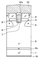
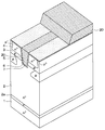
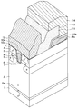
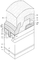
- FIG. 1 is a cross-sectional view of a semiconductor device according to a first embodiment.
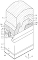
- FIG. 2 is a perspective sectional view of the semiconductor device shown in FIG.
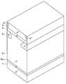
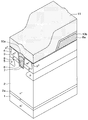
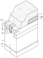
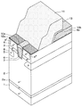
- FIG. 7 is a cross-sectional view showing the manufacturing process of the semiconductor device shown in FIG. 1;
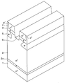
- 3C is a cross-sectional view showing the manufacturing process of the semiconductor device continued from FIG. 3A;
- FIG. 3C is a cross-sectional view showing the manufacturing process of the semiconductor device, following FIG. 3B;
- FIG. 3C is a cross-sectional view showing the manufacturing process of the semiconductor device, following FIG. 3C;
- FIG. 3D is a cross-sectional view showing the manufacturing process of the semiconductor device, following FIG. 3D;
- FIG. 3D is a cross-sectional view showing the manufacturing process of the semiconductor device, following FIG. 3D;
- FIG. 3E is a cross-sectional view showing the manufacturing process of the semiconductor device, following FIG. 3E;
- 3F is a cross-sectional view showing the manufacturing process of the semiconductor device, following FIG. 3F;
- FIG. 3G is a cross-sectional view showing the manufacturing process of the semiconductor device, following FIG. 3G;
- 3J is a cross-sectional view showing the manufacturing process of the semiconductor device, following FIG. 3H;
- FIG. 3E is a cross-sectional view showing the manufacturing process of the semiconductor device, following FIG. 3E;
- 3F is a cross-sectional view showing the manufacturing process of the semiconductor device, following FIG. 3F;
- 3G is a cross-sectional view showing the manufacturing process of the semiconductor device, following FIG. 3G;
- 3J is a cross-sectional view showing the manufacturing process of the semiconductor device, following FIG. 3H;
- FIG. 3H is a cross-sectional view showing the manufacturing process of the semiconductor device, following FIG. 3H;
- the semiconductor device according to the present embodiment is, as shown in FIGS. 1 and 2, formed with a vertical MOSFET as a semiconductor element having a MOS structure.
- the vertical MOSFET is formed in the cell region of the semiconductor device, and the outer peripheral breakdown voltage structure is formed so as to surround the cell region, but the semiconductor device is configured here. Only the gate lead-out portion in the MOSFET is shown.
- the horizontal direction in FIG. 1 and the X direction in FIG. 2 are taken as the width direction
- the vertical direction in FIG. 1 and the Y direction in FIG. 2 as the depth direction
- the Z direction in FIG. 2 will be described as the thickness direction or the depth direction.
- an n + -type substrate 1 made of SiC is used as a semiconductor substrate.
- the depth direction is made to coincide with the off direction.
- an off substrate having a (0001) Si surface and a predetermined off angle is used, and for example, the off direction is set to ⁇ 11-20>.
- the n-type impurity concentration of the n + -type substrate 1 is, eg, 1.0 ⁇ 10 19 / cm 3 .
- n -- type drift layer 2 made of SiC, p-type base region 3 and n + -type source region 4 are epitaxially grown in order.
- the n ⁇ -type drift layer 2 has, for example, an n-type impurity concentration of 0.5 to 2.0 ⁇ 10 16 / cm 3 and a thickness of 5 to 14 ⁇ m.
- n - the boundary between the n + -type substrate 1 of the type drift layer 2, optionally n - even each other by the type drift layer 2 to form a partially high concentration and buffer layer 2a good.
- the p-type base region 3 is a portion where the channel region is formed, and the p-type impurity concentration is, for example, about 2.0 ⁇ 10 17 / cm 3 and the thickness is 0.5 to 2 ⁇ m. Further, in the case of the present embodiment, the surface layer portion of the p-type base region 3 is a contact region in which the p-type impurity concentration is increased.
- the n + -type source region 4 has a higher impurity concentration than the n ⁇ -type drift layer 2 and has an n-type impurity concentration of, for example, 2.5 ⁇ 10 18 to 1.0 ⁇ 10 19 / cm 3 in the surface layer portion. It is composed of about 0.5 to 2 ⁇ m.
- a p-type deep layer 5 is formed in the surface layer portion of the n ⁇ -type drift layer 2, that is, below the p-type base region 3.
- the p-type deep layer 5 has a p-type impurity concentration higher than that of the p-type base region 3, and a plurality of the p-type deep layers 5 are arranged at equal intervals and separated from each other without intersecting each other. It is done.
- each p-type deep layer 5 has a p-type impurity concentration of 1.0 ⁇ 10 17 to 1.0 ⁇ 10 19 / cm 3 and a width of 0.7 ⁇ m.
- Each p-type deep layer 5 has a depth of 0.4 ⁇ m or more, and is formed to a position deeper than the trench gate structure described later, thereby suppressing entry of an electric field into the trench gate structure.
- the p-type deep layer 5 is formed only in the surface layer portion of the n ⁇ -type drift layer 2, but the n ⁇ -type source region 4 and the p-type base region 3 are penetrated to form the n ⁇ -type It may be formed to reach the drift layer 2.
- a trench can be formed from the surface of the n + -type source region 4 and the p-type deep layer 5 can be formed to be embedded in the trench.
- the width is 0.8 ⁇ m and the depth is p-type base region 3 and n + -type source region so as to penetrate p-type base region 3 and n + -type source region 4 to reach n ⁇ -type drift layer 2.
- a gate trench 6 which is 0.2 to 0.4 ⁇ m deeper than the total film thickness of 4 is formed.
- the p-type base region 3 and the n + -type source region 4 described above are arranged in contact with the side surfaces of the gate trench 6.
- the gate trench 6 is formed in a linear layout in which the width direction, the depth direction, and the thickness direction of the vertical MOSFET are respectively the width direction, the longitudinal direction, and the depth direction. Further, although only one is shown in FIGS. 1 and 2, a plurality of gate trenches 6 are arranged at equal intervals in the lateral direction of the paper surface of FIG. It is arranged in the form of stripes.
- a portion of the p-type base region 3 located on the side surface of the gate trench 6 is a channel region connecting the n + -type source region 4 and the n ⁇ -type drift layer 2 when the vertical MOSFET operates.
- a gate insulating film 7 is formed on the inner wall surface of the gate trench 6 including the channel region.
- a gate electrode 8 made of doped polysilicon is formed on the surface of the gate insulating film 7, and the inside of the gate trench 6 is buried with the gate insulating film 7 and the gate electrode 8.
- the gate insulating film 7 may be formed to the outside of the gate trench 6 but is preferably formed only in the gate trench 6.
- a thermal oxide film 10 a corresponding to a first interlayer insulating film formed by thermally oxidizing the surface of the gate electrode 8 is provided on the gate electrode 8.
- the thermal oxide film 10a is formed of a silicon oxide film formed by thermal oxidation, and contains therein an impurity serving as a dopant for the semiconductor. This impurity is the same as that contained in the gate electrode 8 and is, for example, phosphorus (P) or boron (B).
- the thermal oxide film 10a may contain either or both of phosphorus and boron as impurities.
- the thermal oxide film 10 a is formed in the gate trench 6 and is thicker than the portion on the inner wall surface of the gate trench 6 where the channel region is formed in the gate insulating film 7 and thinner than 500 nm. .
- insulation separation between the gate electrode 8 and the source electrode 12 described later can be surely performed.
- is made thinner than 500nm thermal oxide film 10a it can as a gate electrode 8 is accurately positioned on the opposite side to the n + -type source region 4 across the gate insulating film 7, n + -type source region It is not necessary to form 4 to a position deeper than necessary.
- thermal oxide film 10 a has a height of ⁇ 100 nm with respect to the surface of the n + -type source region 4 outside the gate trench 6.
- thermal oxide film 10a has a surface which is at the same height with respect to the surface of n + -type source region 4, or in the inside of gate trench 6 beyond that, or a gate trench further than that. It is in the state of protruding to the outside of 6. Then, if the surface of thermal oxide film 10 a is in a state in which gate trench 6 is inward of the surface of n + type source region 4, the amount of intrusion is 100 nm or less, and protrudes outside gate trench 6. If there is, the protrusion amount is 100 nm or less.
- thermal oxide film 10a As for the height of thermal oxide film 10a, the state in which the surface of thermal oxide film 10a is in the inside of gate trench 6 and the state in which it protrudes outward from the surface of n + type source region 4 are minus and plus, respectively. Is represented by.
- the thermal oxide film 10 a does not extend outside the gate trench 6 in the width direction of the gate trench 6, and is terminated at the inside of the gate trench 6 in the width direction. Therefore, the contact regions of the n + -type source region 4 and the p-type base region 3 are exposed from the thermal oxide film 10 a.
- a plurality of trench gate structures are arranged in a stripe shape.
- the gate electrode 8 is configured so as to connect the ends in the longitudinal direction of the respective trench gate structures, or to connect the intermediate positions in the longitudinal direction of the respective trench gate structures although not shown.
- a gate lead-out portion 8a in which doped polysilicon is left is formed.
- the gate lead-out portion 8 a is formed to protrude above the gate electrode 8, that is, from the SiC surface such as the n + -type source region 4.
- the thermal oxide film 10b is partially disposed on the gate lead-out portion 8a, and the thermal oxide film 10b is formed above the SiC surface such as the n + -type source region 4 in this portion. It has become.
- An interlayer insulating film 11 corresponding to the interlayer insulating film is formed.
- the interlayer insulating film 11 is formed of, for example, BPSG.
- the thickness of the interlayer insulating film 11 is, eg, 600 nm.
- Interlayer insulating film 11 is removed at a position other than on or in the vicinity of gate lead-out portion 8a in the cell region where the vertical MOSFET is formed. Therefore, the gate insulating film 7, the thermal oxide film 10a, the contact region of the p-type base region 3 and the n + -type source region 4 are exposed from the interlayer insulating film 11 at positions other than the gate lead-out portion 8a.
- the source electrode 12 is formed at this exposed position, and is electrically connected to the contact region of the p-type base region 3 and the n + -type source region 4.
- interlayer insulating film 11 is partially removed also on gate lead-out portion 8a.
- the thermal oxide film 10 b is also removed, and the contact hole 13 is formed.
- the gate wiring layer 14 is formed at the position where the contact hole 13 is formed, whereby the gate lead-out portion 8 a is connected.
- the source electrode 12 and the gate wiring layer 14 are made of a plurality of metals such as Ni / Al. Then, at least a portion of the plurality of metals in contact with the n-type SiC, specifically the n + -type source region 4 and the like, is made of a metal that can make an ohmic contact with the n-type SiC. Further, at least a portion of the plurality of metals in contact with the p-type SiC, specifically, the p-type deep layer 5, and the like are made of a metal capable of being in ohmic contact with the p-type SiC. The source electrode 12 and the gate wiring layer 14 are arranged separately from each other, and are electrically insulated by the thermal oxide films 10 a and 10 b and the interlayer insulating film 11.
- the surfaces of the source electrode 12, the gate wiring layer 14 and the interlayer insulating film 11 are covered and protected by a passivation film 15. Then, although not shown, the source electrode 12 and the gate wiring layer 14 are exposed by partially removing the passivation film 15, and are connected to the source pad and the gate pad for external connection.
- n + -type substrate 1 On the back side of the n + -type substrate 1 n + -type substrate 1 and electrically connected to the drain electrode 16 are formed.
- Such a structure constitutes an n-channel type inverted trench gate vertical MOSFET.
- a cell region is configured by arranging a plurality of such vertical MOSFETs in a plurality of cells.
- a semiconductor device is configured by configuring an outer peripheral withstand voltage structure such as a guard ring (not shown) so as to surround a cell region in which such a vertical MOSFET is formed.
- the SiC semiconductor device having the vertical MOSFET configured in this way has a gate voltage Vg of 20 V with respect to the gate electrode 8 in a state where the source voltage Vs is 0 V and the drain voltage Vd is 1 to 1.5 V, for example. It is made to operate by applying. That is, when the gate voltage Vg is applied to the vertical MOSFET, a channel region is formed in the p-type base region 3 in a portion in contact with the gate trench 6, and a current flows between the drain and the source.
- the thermal oxide film 10a is disposed in the gate trench 6. Therefore, it is possible to secure insulation isolation between the gate and the source by the thermal oxide film 10a. Further, while the thermal oxide film 10 a is disposed in the gate trench 6, the thermal oxide film 10 a is configured not to protrude from the gate trench 6 in the width direction of the gate trench 6. Thus, the source electrode 12 is properly brought into contact with the contact region of the p-type base region 3 and the n + -type source region 4. Therefore, the contact of the source electrode 12 can be properly performed.
- the thermal oxide film 10a does not project into the shape of the surface of the SiC, or even if it protrudes, the amount of projection is small. Therefore, it is possible to suppress the occurrence of the crack in the thermal oxide film 10a due to the stress accompanying the temperature change and the like, and it becomes possible to suppress the occurrence of the gate-source leak.
- n + -type substrate 1 is prepared as a semiconductor substrate.
- an n ⁇ -type drift layer 2 made of SiC is formed on the main surface of the n + -type substrate 1 using a chemical vapor deposition (hereinafter referred to as CVD) apparatus or the like.
- CVD chemical vapor deposition
- a buffer layer 2a in which the n ⁇ -type drift layer 2 has a partially high concentration may be formed.
- the p-type deep layer 5 is formed by ion-implanting p-type impurities.
- the mask is removed, and the p-type base region 3 and the n + -type source region 4 are formed on the n ⁇ -type drift layer 2 on which the p-type deep layer 5 is formed.
- the n + -type source region 4 is formed by ion implantation of an n-type impurity.
- the contact region of the p-type base region 3 is formed by ion implantation of a p-type impurity.
- a mask (not shown) is disposed on the surfaces of p type base region 3 and n + type source region 4 to open a region for forming a trench gate structure of the mask.
- the gate trench 6 is formed by performing anisotropic etching such as RIE (Reactive Ion Etching) using a mask. For example, etching is performed with a setting such that the depth of the gate trench 6 is 0.2 to 0.4 ⁇ m deeper than the total film thickness of the p-type base region 3 and the n + -type source region 4.
- RIE Reactive Ion Etching
- the gate insulating film 7 is formed, for example, by thermal oxidation, and the gate insulating film 7 covers the inner wall surface of the gate trench 6 and the surface of the n + -type source region 4.
- polysilicon 20 doped with, for example, an n-type impurity is deposited to form gate electrode 8 and gate lead-out portion 8a, and then this is etched back.
- a mask is disposed so as to cover a portion to be the gate lead-out portion 8a, and the polysilicon 20 is etched back.
- the polysilicon 20 is left in the gate trench 6, and the polysilicon 20 is left to project above the SiC surface at the planned formation position of the gate lead-out portion 8a.
- the polysilicon 20 is removed except in the gate trench 6 and the planned formation position of the gate lead-out portion 8a. Thereafter, the mask used at the time of etch back is removed.
- Step shown in FIG. 3D By heat treatment, the surface of the polysilicon 20 is thermally oxidized.
- the heat treatment is performed, for example, by wet oxidation at 1050 ° C. for 30 minutes.
- the thermal oxidation film 10 a is formed in the gate trench 6 by thermally oxidizing the polysilicon 20, and the remaining polysilicon 20 forms the gate electrode 8.
- the thermal oxide film 10b is also formed on the surface of the polysilicon 20 at the planned formation position of the gate lead-out portion 8a, and the remaining polysilicon 20 forms the gate lead-out portion 8a.
- the thickness of the thermal oxide films 10a and 10b is arbitrary, but the height of the thermal oxide film 10a with respect to the surface of the n + -type source region 4 outside the gate trench 6 after etch back in the step shown in FIG. Is set to be ⁇ 100 nm.
- thermal oxide films 10a and 10b can be formed.
- the thermal oxide films 10a and 10b formed in this manner are those obtained by thermally oxidizing the impurity-doped polysilicon 20, and thus include the impurity serving as the dopant for the semiconductor as the impurity. .
- the thermal oxide films 10a and 10b are higher in height than the polysilicon 20 before thermal oxidation due to volume expansion.
- the heat treatment is performed at a temperature at which the polysilicon 20 is thermally oxidized but the SiC is hardly oxidized. By doing this, the thermal oxide films 10a and 10b are formed while the thickness of the gate insulating film 7 is hardly increased.
- Step shown in FIG. 3E After depositing the interlayer insulating film 11 made of BPSG or the like on the surface of the thermal oxide films 10a and 10b and the gate insulating film 7 using a CVD apparatus or the like, reflow processing is performed.
- the film thickness of the interlayer insulating film 11 at this time is arbitrary, but is thicker than the thermal oxide films 10a and 10b.
- Step shown in FIG. 3F After arranging a mask (not shown) covering a portion corresponding to gate lead-out portion 8a of interlayer insulating film 11, a portion of interlayer insulating film 11 or gate insulating film 7 located outside gate trench 6 and a thermal oxide film Etch back the portion of 10 a that protrudes from the gate trench 6. Specifically, etch back is performed by chemical dry etching (hereinafter referred to as CDE).
- CDE chemical dry etching
- the etching rate at the time of etching back is that of the thermal oxide film 10a. Is slower than the interlayer insulating film 11. That is, the interlayer insulating film 11 is easily etched, and the thermal oxide film 10a can be etched back under the condition that etching is difficult.
- the thermal oxide film 10a is not so etched, which is preferable.
- chemical dry etching is used as chemical etching here, wet etching may be used.
- interlayer insulating film 11 can be completely removed while leaving thermal oxide film 10 a in gate trench 6.
- the gate insulating film 7 formed thinner than the thermal oxide film 10a is also completely or almost completely removed from the portion located outside the gate trench 6, and the n + -type source region 4 and the p-type are formed.
- the contact area of base area 3 is exposed.
- the thermal oxide film 10a functioning as an interlayer insulating film for insulating between the gate and the source remains in the gate trench 6 in a self-aligned manner and is not formed outside the gate trench 6 in the width direction. it can.
- a metal layer 12a for contact made of, for example, Ni is formed. Thereafter, heat treatment is performed as necessary.
- a Ni silicide layer can be formed.
- the planned formation position of the contact hole 13 in the mask is opened, and the interlayer insulating film 11 and the thermal oxide film 10 b are etched to form the contact hole 13.
- a metal layer is formed on the metal layer 12 a and the interlayer insulating film 11 including the inside of the contact hole 13 and patterned to form the source electrode 12 and the gate wiring layer 14.
- a passivation film 15 is formed to cover the source electrode 12 and the gate wiring layer 14 and then patterned to expose desired portions of the source electrode 12 and the gate wiring layer 14.
- insulation between the gate electrode 8 and the source electrode 12 can be performed by the thermal oxide film 10 a configured by thermally oxidizing a part of the gate electrode 8.
- the thermal oxide film 10a configured by thermally oxidizing a part of the gate electrode 8 does not have a shape protruding so much from the SiC surface, it is difficult for a crack due to a stress caused by a temperature change or the like. Therefore, it is possible to secure gate-source insulation isolation.
- the interlayer insulating film 11 is removed from above the contact regions of the n + -type source region 4 and the p-type base region 3 by etch back. Therefore, the source electrode 12 can be properly contacted on both sides of the gate electrode 8.
- the thermal oxide film 10a functioning as an interlayer insulating film for insulating between the gate and the source remains in the gate trench 6 in a self-aligned manner, and can not be formed outside the gate trench 6 in the width direction. Therefore, mass productivity of the SiC semiconductor device can be secured.
- the n-channel vertical MOSFET having the first conductivity type as n-type and the second conductivity type as p-type has been described as an example, but the conductivity type of each component is inverted. It may be a vertical p-channel type MOSFET.
- the vertical MOSFET is described as an example of the semiconductor element having the MOS structure.
- the present disclosure can be applied to an IGBT having a similar MOS structure.
- the conductivity type of the n + -type substrate 1 is merely changed from n-type to p-type in each of the above embodiments, and the other structure and manufacturing method are the same as in the above embodiments. It is.
- a bar (-) should normally be added above the desired number, but since there is a limitation in expression based on the electronic application, it is desirable in the present specification to be a desired one. A bar shall be put in front of the numbers.
Landscapes
- Electrodes Of Semiconductors (AREA)
- Formation Of Insulating Films (AREA)
Abstract
ゲート電極(8)の一部を熱酸化して形成した熱酸化膜(10a)を第1の層間絶縁膜としてゲート電極(8)とソース電極(12)との絶縁を行う。ゲート電極(8)の一部を熱酸化することで構成した熱酸化膜はSiC表面からあまり突き出た形状にならないため、温度変化などに伴う応力によるクラックが入り難い。したがって、ゲート-ソース間の絶縁分離を担保することが可能となる。また、第2の層間絶縁膜(11)については、エッチバックによってソース領域(4)およびベース領域(3)のコンタクト領域の上から除去されるようにしている。このため、ゲート電極(8)を挟んだ両側において、ソース電極(12)のコンタクトを的確に行うことが可能となる。
Description
本出願は、2017年9月27日に出願された日本特許出願番号2017-186917号に基づくもので、ここにその記載内容が参照により組み入れられる。
本発明は、炭化珪素(以下、SiCという)によって構成されるトレンチゲート型のMOS構造の半導体素子を有するSiC半導体装置およびその製造方法に関するものである。
従来より、パワーデバイスとして、SiCを用いたMOSFETが開発されている。MOSFETでは、ゲート電極とソース電極との間を絶縁分離するために、層間絶縁膜を形成している(特開2011-101036号公報参照)。例えば、ゲート電極の形成後に、ゲート電極を覆うように層間絶縁膜としてPSG(Phosphorous Silicate Glass)またはBPSG(Boro-phospho silicate glass)を成膜する。続いて、フォトリソグラフィ・エッチングにより、層間絶縁膜に対してソースコンタクト用のコンタクトホールを形成する。そして、アニール処理によって層間絶縁膜を丸めたのち、層間絶縁膜の上に電極材料を成膜し、さらにこれをパターニングすることでソース電極を形成する。このようにして、ゲート電極とソース電極との間が層間絶縁膜によって絶縁分離された構造を構成している。
しかしながら、層間絶縁膜にコンタクトホールを形成する際のマスクずれにより、ゲート電極とソース電極との間の絶縁分離が確保できず、ゲート-ソース間リークを生じさせるという課題が発生する。また、ゲート電極を挟んで一方側ではソース電極のコンタクトが行えても、もう一方側ではソース電極のコンタクトが行えなくなるという課題を発生させることもある。そして、これらの課題は、素子の微細化が進むほど発生し易く、ステッパのアライメント許容限界を超える精度要求となることから、SiC半導体装置の量産が難しくなり得る。
また、層間絶縁膜がSiC表面に対して突き出す形状となるため、温度変化などに伴う応力によって層間絶縁膜にクラックが入り、ゲート-ソース間リークを発生させる一因になっていた。
本開示は、ゲート-ソース間の絶縁分離を担保しつつ、ソース電極のコンタクトを的確に行うことができる構造のSiC半導体装置およびその製造方法を提供することを目的とする。
本開示の1つの観点におけるSiC半導体装置では、SiCで構成された第1または第2導電型の基板と、基板の上に形成され、基板よりも低不純物濃度とされた第1導電型のSiCからなるドリフト層と、ドリフト層の上に形成された第2導電型のSiCからなるベース領域と、ベース領域の上に形成され、ドリフト層よりも第1導電型不純物濃度が高くされた第1導電型のSiCからなるソース領域と、ソース領域の表面からベース領域よりも深く形成されたゲートトレンチ内に、該ゲートトレンチの内壁面を覆うゲート絶縁膜と該ゲート絶縁膜の上に配置されると共に不純物がドープされたゲート電極とを備えて構成されたトレンチゲート構造と、ゲート電極およびゲート絶縁膜を覆うと共に、ゲートトレンチ内に配置され、ゲート電極にドープされた不純物が含まれる熱酸化膜で構成された層間絶縁膜と、層間絶縁膜とソース領域およびベース領域の表面上に形成され、ソース領域およびベース領域に電気的に接続されたソース電極と、基板の裏面側に形成されたドレイン電極と、を含んでいる。
このように、ゲート電極の一部を熱酸化することによって構成した熱酸化膜によってゲート電極とソース電極との絶縁を行っている。また、ゲート電極の一部を熱酸化することで構成した熱酸化膜はSiC表面からあまり突き出た形状にならないため、温度変化などに伴う応力によるクラックが入り難い。したがって、ゲート-ソース間の絶縁分離を担保することが可能となる。さらに、ゲート電極の一部を熱酸化した熱酸化膜によってゲート-ソース間を絶縁できるため、半導体素子として機能させられる部分において、ソース領域およびベース領域の表面上には層間絶縁膜が形成されないようにエッチバックすれば良い。このため、ゲート電極を挟んだ両側において、ソース電極のコンタクトを的確に行うことが可能となる。
なお、各構成要素等に付された括弧付きの参照符号は、その構成要素等と後述する実施形態に記載の具体的な構成要素等との対応関係の一例を示すものである。
以下、本開示の実施形態について図に基づいて説明する。なお、以下の各実施形態相互において、互いに同一もしくは均等である部分には、同一符号を付して説明を行う。
(第1実施形態)
第1実施形態について説明する。本実施形態にかかる半導体装置は、図1および図2に示すように、MOS構造の半導体素子として縦型MOSFETが形成されたものである。縦型MOSFETは、半導体装置のうちのセル領域に形成されており、そのセル領域を囲むように外周耐圧構造が形成されることで半導体装置が構成されているが、ここでは縦型MOSFETおよび縦型MOSFETにおけるゲート引出部のみ図示してある。なお、以下の説明では、縦型MOSFETのうち、図1の左右方向および図2のX方向を幅方向とし、図1の紙面垂直方向および図2のY方向を奥行方向、図1の上下方向および図2のZ方向を厚み方向もしくは深さ方向として説明を行う。
第1実施形態について説明する。本実施形態にかかる半導体装置は、図1および図2に示すように、MOS構造の半導体素子として縦型MOSFETが形成されたものである。縦型MOSFETは、半導体装置のうちのセル領域に形成されており、そのセル領域を囲むように外周耐圧構造が形成されることで半導体装置が構成されているが、ここでは縦型MOSFETおよび縦型MOSFETにおけるゲート引出部のみ図示してある。なお、以下の説明では、縦型MOSFETのうち、図1の左右方向および図2のX方向を幅方向とし、図1の紙面垂直方向および図2のY方向を奥行方向、図1の上下方向および図2のZ方向を厚み方向もしくは深さ方向として説明を行う。
半導体装置には、SiCからなるn+型基板1が半導体基板として用いられている。本実施形態の場合、奥行方向がオフ方向と一致させられている。n+型基板1としては、表面が(0001)Si面とされていて、所定のオフ角を有したオフ基板が用いられており、例えばオフ方向が<11-20>とされている。n+型基板1のn型不純物濃度は、例えば1.0×10¹⁹/cm3とされている。
n+型基板1の主表面上には、SiCからなるn-型ドリフト層2、p型ベース領域3およびn+型ソース領域4が順にエピタキシャル成長させられている。
n-型ドリフト層2は、例えばn型不純物濃度が0.5~2.0×10¹⁶/cm3とされ、厚さが5~14μmとされている。なお、n-型ドリフト層2のうちn+型基板1との境界位置には、必要に応じてn-型ドリフト層2を部分的に高濃度としたバッファ層2aを形成してあっても良い。
p型ベース領域3は、チャネル領域が形成される部分で、p型不純物濃度が例えば2.0×10¹⁷/cm3程度とされ、厚みが0.5~2μmで構成されている。また、本実施形態の場合、p型ベース領域3のうちの表層部はp型不純物濃度が高くされたコンタクト領域とされている。
n+型ソース領域4は、n-型ドリフト層2よりも高不純物濃度とされ、表層部におけるn型不純物濃度が例えば2.5×10¹⁸~1.0×10¹⁹/cm3、厚さ0.5~2μm程度で構成されている。
また、n-型ドリフト層2の表層部、つまりp型ベース領域3の下方には、p型ディープ層5が形成されている。p型ディープ層5は、p型ベース領域3よりもp型不純物濃度が高くされており、複数本が等間隔に配置され、互いに交点なく離れて配置されることで、上面レイアウトがストライプ状とされている。例えば、各p型ディープ層5は、p型不純物濃度が1.0×10¹⁷~1.0×10¹⁹/cm3、幅0.7μmとされている。また、各p型ディープ層5は、深さが0.4μm以上の深さとされ、後述するトレンチゲート構造よりも深い位置まで形成されることで、トレンチゲート構造への電界の入り込みを抑制する。
なお、本実施形態では、p型ディープ層5をn-型ドリフト層2の表層部にのみ形成した構造としたが、n+型ソース領域4やp型ベース領域3を貫通してn-型ドリフト層2に達するように形成しても良い。例えば、n+型ソース領域4の表面からトレンチを形成し、このトレンチ内を埋め込むようにp型ディープ層5を形成することもできる。
また、p型ベース領域3およびn+型ソース領域4を貫通してn-型ドリフト層2に達するように、例えば幅が0.8μm、深さがp型ベース領域3とn+型ソース領域4の合計膜厚よりも0.2~0.4μm深くされたゲートトレンチ6が形成されている。このゲートトレンチ6の側面と接するように上述したp型ベース領域3およびn+型ソース領域4が配置されている。ゲートトレンチ6は、縦型MOSFETの幅方向、奥行方向、厚み方向をそれぞれ幅方向、長手方向、深さ方向とするライン状のレイアウトで形成されている。また、図1および図2には1本しか示していないが、ゲートトレンチ6は、複数本が図1の紙面左右方向に等間隔に配置され、それぞれp型ディープ層5の間に挟まれるように配置されていてストライプ状とされている。
p型ベース領域3のうちゲートトレンチ6の側面に位置している部分は、縦型MOSFETの作動時にn+型ソース領域4とn-型ドリフト層2との間を繋ぐチャネル領域とされる。このチャネル領域を含むゲートトレンチ6の内壁面に、ゲート絶縁膜7が形成されている。そして、ゲート絶縁膜7の表面にはドープドポリシリコンで構成されたゲート電極8が形成されており、これらゲート絶縁膜7およびゲート電極8によってゲートトレンチ6内が埋め込まれている。このようにして、トレンチゲート構造が構成されている。なお、ゲート絶縁膜7は、ゲートトレンチ6の外側まで形成されていても良いが、ゲートトレンチ6内のみに形成されていると好ましい。
ゲート電極8の上には、ゲート電極8の表面を熱酸化することによって形成された第1の層間絶縁膜に相当する熱酸化膜10aが備えられている。熱酸化膜10aは、熱酸化によって形成されたシリコン酸化膜によって構成されており、内部に、半導体に対するドーパントとなる不純物が含まれている。この不純物は、ゲート電極8に含まれているものと同じものであり、例えばリン(P)やボロン(B)などとされている。熱酸化膜10a内に、不純物としてリンとボロンのいずれか一方が含まれていても良いし、両方が含まれていても良い。
熱酸化膜10aは、ゲートトレンチ6内に形成されており、ゲート絶縁膜7のうちゲートトレンチ6におけるチャネル領域が形成される内壁面上の部分よりも厚く、かつ、500nmよりも薄くされている。熱酸化膜10aの厚みがゲート絶縁膜7よりも厚くされることによりゲート電極8と後述するソース電極12との間の絶縁分離を確実に行えるようにしている。また、熱酸化膜10aを500nmよりも薄くすることで、ゲート絶縁膜7を挟んでn+型ソース領域4と反対側にゲート電極8が的確に配置されるようにでき、n+型ソース領域4を必要以上に深い位置まで形成しなくても済むようにできる。
また、熱酸化膜10aは、ゲートトレンチ6の外側におけるn+型ソース領域4の表面に対して±100nmの高さとされている。具体的には、熱酸化膜10aは、その表面がn+型ソース領域4の表面に対して同じ高さか、それよりもゲートトレンチ6の内側に入り込んでいる状態、もしくは、それよりもゲートトレンチ6の外側に突き出した状態となっている。そして、熱酸化膜10aの表面がn+型ソース領域4の表面よりもゲートトレンチ6の内側に入り込んでいる状態であれば、その入り込み量が100nm以下、ゲートトレンチ6の外側に突き出した状態であれば、その突き出し量が100nm以下となっている。なお、熱酸化膜10aの高さについては、熱酸化膜10aの表面がn+型ソース領域4の表面よりもゲートトレンチ6の内側に入り込んでいる状態と外側に突き出した状態をそれぞれマイナスとプラスで表している。
また、熱酸化膜10aは、ゲートトレンチ6の幅方向においてはゲートトレンチ6の外側には張り出しておらず、ゲートトレンチ6に幅方向の内側において終端させられた状態となっている。このため、n+型ソース領域4およびp型ベース領域3のコンタクト領域が熱酸化膜10aから露出させられた状態となっている。
なお、セル領域において、トレンチゲート構造が複数本ストライプ状に配置されている。そして、図2に示すように各トレンチゲート構造の長手方向の先端を繋ぐように、もしくは、図示していないが各トレンチゲート構造の長手方向の中間位置を繋ぐように、ゲート電極8を構成するドープドポリシリコンが残されたゲート引出部8aが形成されている。ゲート引出部8aは、ゲート電極8の上方、つまりn+型ソース領域4等のSiC表面から突き出すように形成されている。このゲート引出部8aの上にも部分的に熱酸化膜10bが配置されており、この部分に関しては、n+型ソース領域4等のSiC表面よりも上方に熱酸化膜10bが形成された状態になっている。
また、ゲート引出部8aの近傍では、ゲート絶縁膜7や熱酸化膜10a、10bの上を含めて、p型ベース領域3のコンタクト領域およびn+型ソース領域4の表面上に、第2の層間絶縁膜に相当する層間絶縁膜11が形成されている。層間絶縁膜11は、例えばBPSGなどによって形成されている。層間絶縁膜11をBPSGによって構成する場合、層間絶縁膜11の厚みは例えば600nmとされる。
層間絶縁膜11は、縦型MOSFETが形成されるセル領域のうちゲート引出部8aの上やその近傍以外の位置では除去されている。このため、ゲート引出部8a以外の位置では、ゲート絶縁膜7、熱酸化膜10a、p型ベース領域3のコンタクト領域およびn+型ソース領域4が層間絶縁膜11から露出している。そして、この露出している位置にはソース電極12が形成されており、p型ベース領域3のコンタクト領域およびn+型ソース領域4と電気的に接続させられている。
さらに、層間絶縁膜11は、ゲート引出部8aの上においても部分的に除去されている。この部分では、熱酸化膜10bも除去されており、コンタクトホール13が形成されている。そして、このコンタクトホール13が形成されている位置にゲート配線層14が形成されることでゲート引出部8aと接続されている。
ソース電極12やゲート配線層14は、複数の金属、例えばNi/Al等にて構成されている。そして、複数の金属のうち少なくともn型SiC、具体的にはn+型ソース領域4などと接触する部分はn型SiCとオーミック接触可能な金属で構成されている。また、複数の金属のうち少なくともp型SiC、具体的にはp型ディープ層5と接触する部分などはp型SiCとオーミック接触可能な金属で構成されている。なお、ソース電極12やゲート配線層14は、互いに分離されて配置されており、熱酸化膜10a、10bおよび層間絶縁膜11によって電気的に絶縁されている。
なお、ソース電極12やゲート配線層14および層間絶縁膜11の表面はパッシベーション膜15によって覆われていて保護されている。そして、図示しないが、パッシベーション膜15が部分的に除去されることでソース電極12やゲート配線層14が露出させられており、外部接続用のソースパッドやゲートパッドと接続されている。
さらに、n+型基板1の裏面側にはn+型基板1と電気的に接続されたドレイン電極16が形成されている。このような構造により、nチャネルタイプの反転型のトレンチゲート構造の縦型MOSFETが構成されている。このような縦型MOSFETが複数セル配置されることでセル領域が構成されている。そして、このような縦型MOSFETが形成されたセル領域を囲むように図示しないガードリングなどによる外周耐圧構造が構成されることで半導体装置が構成されている。
このように構成された縦型MOSFETを有するSiC半導体装置は、例えば、ソース電圧Vsを0V、ドレイン電圧Vdを1~1.5Vとした状態で、ゲート電極8に対して20Vのゲート電圧Vgを印加することで動作させられる。すなわち、縦型MOSFETは、ゲート電圧Vgが印加されることにより、ゲートトレンチ6に接する部分のp型ベース領域3にチャネル領域を形成し、ドレイン-ソース間に電流を流すという動作を行う。
このような動作を的確に行うためには、ゲート-ソース間リークが生じないように熱酸化膜10aによってゲート-ソース間の絶縁分離が担保されていることや、ソース電極12のコンタクトが的確に行えていることが重要である。これに対して、本実施形態の半導体装置では、熱酸化膜10aがゲートトレンチ6内に配置された状態となっている。このため、熱酸化膜10aによってゲート-ソース間の絶縁分離を担保することが可能となる。また、熱酸化膜10aがゲートトレンチ6内に配置されるようにしつつ、ゲートトレンチ6の幅方向においてはゲートトレンチ6から張り出さないようにしている。これにより、ソース電極12がp型ベース領域3のコンタクト領域およびn+型ソース領域4に的確に接触させられている。このため、ソース電極12のコンタクトが的確に行えている。
このように、熱酸化膜10aによるゲート-ソース間の絶縁分離を担保しつつ、ソース電極12のコンタクトを的確に行うことができる構造のSiC半導体装置とすることが可能となる。
また、MOSFETとして動作させられる領域では、熱酸化膜10aがSiC表面に対して突き出す形状とならない、もしくは、突き出していたとしてもその突き出し量が小さい。したがって、温度変化などに伴う応力により熱酸化膜10aにクラックが入ることが抑制され、ゲート-ソース間リークを発生を抑制することが可能となる。
次に、本実施形態にかかる縦型MOSFETを備えた半導体装置の製造方法について、図3A~図3Hを参照して説明する。
〔図3Aに示す工程〕
まず、半導体基板として、ウェハ状のn+型基板1を用意する。そして、化学気相成長(以下、CVDという)装置などを用いて、このn+型基板1の主表面上にSiCからなるn-型ドリフト層2を形成する。このとき、必要に応じて、n-型ドリフト層2を部分的に高濃度としたバッファ層2aを形成しても良い。そして、図示しないが、p型ディープ層5の形成予定領域が開口するマスクを配置したのち、p型不純物をイオン注入することで、p型ディープ層5を形成する。
まず、半導体基板として、ウェハ状のn+型基板1を用意する。そして、化学気相成長(以下、CVDという)装置などを用いて、このn+型基板1の主表面上にSiCからなるn-型ドリフト層2を形成する。このとき、必要に応じて、n-型ドリフト層2を部分的に高濃度としたバッファ層2aを形成しても良い。そして、図示しないが、p型ディープ層5の形成予定領域が開口するマスクを配置したのち、p型不純物をイオン注入することで、p型ディープ層5を形成する。
その後、マスクを除去してから、p型ディープ層5を形成したn-型ドリフト層2の上に、p型ベース領域3およびn+型ソース領域4を形成する。例えば、p型ベース領域3をエピタキシャル成長させたのち、n型不純物をイオン注入することでn+型ソース領域4を形成する。または、p型ベース領域3およびn+型ソース領域4をエピタキシャル成長させたのち、p型不純物をイオン注入することでp型ベース領域3のコンタクト領域を形成する。これらの工程により、p型ベース領域3およびn+型ソース領域4を形成できる。
〔図3Bに示す工程〕
次に、p型ベース領域3およびn+型ソース領域4の表面に図示しないマスクを配置し、マスクのうちのトレンチゲート構造の形成予定領域を開口させる。そして、マスクを用いてRIE(Reactive Ion Etching)などの異方性エッチングを行うことにより、ゲートトレンチ6を形成する。例えば、ゲートトレンチ6の深さをp型ベース領域3とn+型ソース領域4の合計膜厚よりも0.2~0.4μm深くするという設定としてエッチングを行う。これにより、p型ベース領域3の底部からのゲートトレンチ6の突き出し量が0.2~0.4μmとなるようにしている。
次に、p型ベース領域3およびn+型ソース領域4の表面に図示しないマスクを配置し、マスクのうちのトレンチゲート構造の形成予定領域を開口させる。そして、マスクを用いてRIE(Reactive Ion Etching)などの異方性エッチングを行うことにより、ゲートトレンチ6を形成する。例えば、ゲートトレンチ6の深さをp型ベース領域3とn+型ソース領域4の合計膜厚よりも0.2~0.4μm深くするという設定としてエッチングを行う。これにより、p型ベース領域3の底部からのゲートトレンチ6の突き出し量が0.2~0.4μmとなるようにしている。
〔図3Cに示す工程〕
マスクを除去した後、例えば熱酸化を行うことによって、ゲート絶縁膜7を形成し、ゲート絶縁膜7によってゲートトレンチ6の内壁面上およびn+型ソース領域4の表面上を覆う。そして、ゲート電極8およびゲート引出部8aを形成すべく、例えばn型不純物がドープされたポリシリコン20をデポジションした後、これをエッチバックする。このとき、ゲート引出部8aとなる部分を覆うようにマスクを配置してポリシリコン20をエッチバックするようにしている。これにより、ゲートトレンチ6内にポリシリコン20が残されると共に、ゲート引出部8aの形成予定位置においてSiC表面よりも上方に突き出すようにポリシリコン20が残される。また、ゲートトレンチ6内およびゲート引出部8aの形成予定位置以外においてはポリシリコン20が除去された状態となる。その後、エッチバック時に使用したマスクを除去する。
マスクを除去した後、例えば熱酸化を行うことによって、ゲート絶縁膜7を形成し、ゲート絶縁膜7によってゲートトレンチ6の内壁面上およびn+型ソース領域4の表面上を覆う。そして、ゲート電極8およびゲート引出部8aを形成すべく、例えばn型不純物がドープされたポリシリコン20をデポジションした後、これをエッチバックする。このとき、ゲート引出部8aとなる部分を覆うようにマスクを配置してポリシリコン20をエッチバックするようにしている。これにより、ゲートトレンチ6内にポリシリコン20が残されると共に、ゲート引出部8aの形成予定位置においてSiC表面よりも上方に突き出すようにポリシリコン20が残される。また、ゲートトレンチ6内およびゲート引出部8aの形成予定位置以外においてはポリシリコン20が除去された状態となる。その後、エッチバック時に使用したマスクを除去する。
〔図3Dに示す工程〕
熱処理を行うことで、ポリシリコン20の表面を熱酸化する。熱処理については、例えば1050℃で30分間のウェット酸化によって行っている。これにより、ゲートトレンチ6内においては、ポリシリコン20が熱酸化されることによって熱酸化膜10aが形成された状態となり、残りのポリシリコン20によってゲート電極8が構成される。また、ゲート引出部8aの形成予定位置におけるポリシリコン20についても、表面に、熱酸化膜10bが形成された状態となり、残りのポリシリコン20によってゲート引出部8aが構成される。熱酸化膜10a、10bの厚みについては任意であるが、後述する図3Fに示す工程で行うエッチバック後に、熱酸化膜10aのゲートトレンチ6の外側におけるn+型ソース領域4の表面に対する高さが±100nmとなるように設定してある。
熱処理を行うことで、ポリシリコン20の表面を熱酸化する。熱処理については、例えば1050℃で30分間のウェット酸化によって行っている。これにより、ゲートトレンチ6内においては、ポリシリコン20が熱酸化されることによって熱酸化膜10aが形成された状態となり、残りのポリシリコン20によってゲート電極8が構成される。また、ゲート引出部8aの形成予定位置におけるポリシリコン20についても、表面に、熱酸化膜10bが形成された状態となり、残りのポリシリコン20によってゲート引出部8aが構成される。熱酸化膜10a、10bの厚みについては任意であるが、後述する図3Fに示す工程で行うエッチバック後に、熱酸化膜10aのゲートトレンチ6の外側におけるn+型ソース領域4の表面に対する高さが±100nmとなるように設定してある。
このようにして、熱酸化膜10a、10bを形成することができる。そして、このように形成された熱酸化膜10a、10bは、不純物がドープされたポリシリコン20を熱酸化したものであるため、不純物として半導体に対しるドーパントとなる不純物が含まれたものとなる。
なお、ポリシリコン20を熱酸化した場合、体積膨張により、熱酸化される前のポリシリコン20に対して熱酸化膜10a、10bの方が高さが高くなった状態となる。なお、熱処理については、ポリシリコン20については熱酸化されるがSiCについてはほぼ酸化されない程度の温度で行うようにしている。このようにすることで、ゲート絶縁膜7については殆ど厚みが増えないようにしつつ、熱酸化膜10a、10bが形成されるようにしている。
〔図3Eに示す工程〕
CVD装置などを用いて、熱酸化膜10a、10bやゲート絶縁膜7の表面上にBPSGなどで構成される層間絶縁膜11をデポジションしたのち、リフロー処理を行う。このときの層間絶縁膜11の膜厚については任意であるが、熱酸化膜10a、10bよりも厚くしてある。
CVD装置などを用いて、熱酸化膜10a、10bやゲート絶縁膜7の表面上にBPSGなどで構成される層間絶縁膜11をデポジションしたのち、リフロー処理を行う。このときの層間絶縁膜11の膜厚については任意であるが、熱酸化膜10a、10bよりも厚くしてある。
〔図3Fに示す工程〕
層間絶縁膜11のうちのゲート引出部8aと対応する部分を覆う図示しないマスクを配置したのち、層間絶縁膜11やゲート絶縁膜7のうちのゲートトレンチ6の外側に位置する部分および熱酸化膜10aのうちのゲートトレンチ6から突き出した部分をエッチバックする。具体的には、ケミカルドライエッチング(以下、CDEという)によってエッチバックを行っている。
層間絶縁膜11のうちのゲート引出部8aと対応する部分を覆う図示しないマスクを配置したのち、層間絶縁膜11やゲート絶縁膜7のうちのゲートトレンチ6の外側に位置する部分および熱酸化膜10aのうちのゲートトレンチ6から突き出した部分をエッチバックする。具体的には、ケミカルドライエッチング(以下、CDEという)によってエッチバックを行っている。
このとき、熱酸化によって形成した熱酸化膜10aの方がCVD法によって形成された層間絶縁膜11よりも緻密な膜となっていることから、エッチバックしたときのエッチングレートが熱酸化膜10aの方が層間絶縁膜11よりも遅くなる。つまり、層間絶縁膜11はエッチングされ易く、熱酸化膜10aはエッチングされ難い条件でエッチバックすることが可能となる。特に、CDEのように化学的エッチングの場合、熱酸化膜10aがあまりエッチングされないため好ましい。なお、ここでは化学的エッチングとしてケミカルドライエッチングを用いているが、ウェットエッチングでも良い。
これにより、ゲートトレンチ6内に熱酸化膜10aを残しつつ、層間絶縁膜11を完全に除去することが可能となる。また、熱酸化膜10aよりも薄く形成されたゲート絶縁膜7についても、ゲートトレンチ6の外側に位置している部分については、完全に、もしくはほぼ除去され、n+型ソース領域4およびp型ベース領域3のコンタクト領域が露出させられた状態となる。このようにして、ゲート-ソース間を絶縁するための層間絶縁膜として機能する熱酸化膜10aが自己整合的にゲートトレンチ6内に残り、ゲートトレンチ6の幅方向の外側には形成されないようにできる。
〔図3Gに示す工程〕
ソース電極12のうち、例えばNiなどで構成されるコンタクト用の金属層12aを成膜する。その後、必要に応じて熱処理を行う。これにより、例えば金属層12aとしてNiを用いた場合であれば、Niシリサイド層を構成することができる。
ソース電極12のうち、例えばNiなどで構成されるコンタクト用の金属層12aを成膜する。その後、必要に応じて熱処理を行う。これにより、例えば金属層12aとしてNiを用いた場合であれば、Niシリサイド層を構成することができる。
さらに、図示しないマスクを配置したのち、マスクのうちのコンタクトホール13の形成予定位置を開口させ、層間絶縁膜11および熱酸化膜10bをエッチングすることでコンタクトホール13を形成する。
〔図3Hに示す工程〕
コンタクトホール13内を含めて金属層12aおよび層間絶縁膜11の上に金属層を形成し、これをパターニングすることで、ソース電極12やゲート配線層14を構成する。
コンタクトホール13内を含めて金属層12aおよび層間絶縁膜11の上に金属層を形成し、これをパターニングすることで、ソース電極12やゲート配線層14を構成する。
〔図3Iに示す工程〕
ソース電極12やゲート配線層14などを覆うようにパッシベーション膜15を形成したのち、パターニングしてソース電極12やゲート配線層14のうちの所望部分を露出させる。
ソース電極12やゲート配線層14などを覆うようにパッシベーション膜15を形成したのち、パターニングしてソース電極12やゲート配線層14のうちの所望部分を露出させる。
この後の工程については図示しないが、n+型基板1の裏面側にドレイン電極16を形成するなどの工程を行うことで、図1に示した本実施形態にかかる縦型MOSFETを有する半導体装置が完成する。
以上説明したように、本実施形態の半導体装置では、ゲート電極8の一部を熱酸化することによって構成した熱酸化膜10aによってゲート電極8とソース電極12との絶縁が行えるようにしている。また、ゲート電極8の一部を熱酸化することで構成した熱酸化膜10aはSiC表面からあまり突き出た形状にならないため、温度変化などに伴う応力によるクラックが入り難い。したがって、ゲート-ソース間の絶縁分離を担保することが可能となる。
また、層間絶縁膜11については、エッチバックによってn+型ソース領域4およびp型ベース領域3のコンタクト領域の上から除去されるようにしている。このため、ゲート電極8を挟んだ両側において、ソース電極12のコンタクトを的確に行うことが可能となる。
したがって、ゲート-ソース間の絶縁分離を担保しつつ、ソース電極12のコンタクトを的確に行うことができる構造のSiC半導体装置とすることが可能となる。また、ゲート電極8の一部を熱酸化することで構成した熱酸化膜10aを用いてゲート-ソース間を絶縁する場合、微細化が進んでも的確にゲート-ソース間の絶縁を確保することが可能となる。
また、ゲート-ソース間を絶縁するための層間絶縁膜として機能する熱酸化膜10aが自己整合的にゲートトレンチ6内に残り、ゲートトレンチ6の幅方向の外側には形成されないようにできる。このため、SiC半導体装置の量産性を確保することが可能となる。
(他の実施形態)
本開示は、上記した実施形態に準拠して記述されたが、当該実施形態に限定されるものではなく、様々な変形例や均等範囲内の変形をも包含する。加えて、様々な組み合わせや形態、さらには、それらに一要素のみ、それ以上、あるいはそれ以下、を含む他の組み合わせや形態をも、本開示の範疇や思想範囲に入るものである。
本開示は、上記した実施形態に準拠して記述されたが、当該実施形態に限定されるものではなく、様々な変形例や均等範囲内の変形をも包含する。加えて、様々な組み合わせや形態、さらには、それらに一要素のみ、それ以上、あるいはそれ以下、を含む他の組み合わせや形態をも、本開示の範疇や思想範囲に入るものである。
例えば、上記各実施形態では、第1導電型をn型、第2導電型をp型としたnチャネルタイプの縦型MOSFETを例に挙げて説明したが、各構成要素の導電型を反転させたpチャネルタイプの縦型MOSFETとしても良い。また、上記説明では、MOS構造を有する半導体素子として縦型MOSFETを例に挙げて説明したが、同様のMOS構造を有するIGBTに対しても本開示を適用することができる。nチャネルタイプのIGBTの場合、上記各実施形態に対してn+型基板1の導電型をn型からp型に変更するだけであり、その他の構造や製造方法に関しては上記各実施形態と同様である。
なお、結晶の方位を示す場合、本来ならば所望の数字の上にバー(-)を付すべきであるが、電子出願に基づく表現上の制限が存在するため、本明細書においては、所望の数字の前にバーを付すものとする。
Claims (6)
- MOS構造の半導体素子を有する炭化珪素半導体装置であって、
炭化珪素で構成された第1または第2導電型の基板(1)と、
前記基板の上に形成され、前記基板よりも低不純物濃度とされた第1導電型の炭化珪素からなるドリフト層(2)と、
前記ドリフト層の上に形成された第2導電型の炭化珪素からなるベース領域(3)と、
前記ベース領域の上に形成され、前記ドリフト層よりも第1導電型不純物濃度が高くされた第1導電型の炭化珪素からなるソース領域(4)と、
前記ソース領域の表面から前記ベース領域よりも深く形成されたゲートトレンチ(6)内に、該ゲートトレンチの内壁面を覆うゲート絶縁膜(7)と該ゲート絶縁膜の上に配置されると共に不純物がドープされたゲート電極(8)とを備えて構成されたトレンチゲート構造と、
前記ゲート電極および前記ゲート絶縁膜を覆うと共に、前記ゲートトレンチ内に配置され、前記ゲート電極にドープされた不純物が含まれる熱酸化膜で構成された層間絶縁膜(10a)と、
前記層間絶縁膜と前記ソース領域および前記ベース領域の表面上に形成され、前記ソース領域および前記ベース領域に電気的に接続されたソース電極(12)と、
前記基板の裏面側に形成されたドレイン電極(16)と、を含み、
前記ゲート電極に対してゲート電圧が印加されると、前記ベース領域のうち前記トレンチゲート構造と接する部分にチャネル領域を形成することで電流を流す半導体素子を有した炭化珪素半導体装置。 - 前記層間絶縁膜は、前記ゲートトレンチの外部における前記ソース領域の表面に対して同じ高さか、該表面よりも前記ゲートトレンチの内側に100nm以内入り込んでいる状態、もしくは、該表面よりも前記ゲートトレンチの外側に100nm以内突き出した状態とされている請求項1に記載の炭化珪素半導体装置。
- 前記層間絶縁膜は、前記ゲート絶縁膜のうち前記ゲートトレンチにおける前記チャネル領域が形成される内壁面上の部分よりも厚くされている請求項1または2に記載の炭化珪素半導体装置。
- 前記層間絶縁膜は、500nmよりも薄くされている請求項1ないし3のいずれか1つに記載の炭化珪素半導体装置。
- 前記層間絶縁膜は、前記半導体素子として動作させられる領域では、前記ゲートトレンチの幅方向の内側において終端させられている請求項1ないし4のいずれか1つに記載の炭化珪素半導体装置。
- MOS構造の半導体素子を有する炭化珪素半導体装置の製造方法であって、
炭化珪素で構成された第1または第2導電型の基板(1)を用意することと、
前記基板の上に、前記基板よりも低不純物濃度の第1導電型の炭化珪素からなるドリフト層(2)を形成することと、
前記ドリフト層の上に、第2導電型の炭化珪素からなるベース領域(3)を形成することと、
前記ベース領域の上に、前記ドリフト層よりも第1導電型不純物濃度が高くされた第1導電型の半導体からなるソース領域(4)を形成することと、
前記ソース領域の表面から前記ベース領域よりも深いゲートトレンチ(6)を形成したのち、前記ゲートトレンチの内壁面にゲート絶縁膜(7)を形成すると共に、前記ゲート絶縁膜の上に不純物がドープされたポリシリコンによって構成されるゲート電極(8)を形成することでトレンチゲート構造を形成することと、
前記ゲート電極を熱酸化することで、熱酸化膜による第1の層間絶縁膜(10a)を形成することと、
前記第1の層間絶縁膜の上に、化学気相成長によって第2の層間絶縁膜(11)を形成することと、
前記半導体素子として動作させる領域において、前記ソース領域および前記ベース領域を露出させるまで前記第2の層間絶縁膜を除去しつつ、前記第1の層間絶縁膜が前記ゲートトレンチ内に残るように、前記第1の層間絶縁膜および前記第2の層間絶縁膜をエッチバックすることと、
前記ソース領域および前記ベース領域に電気的に接続されつつ、前記第1の層間絶縁膜によって前記ゲート絶縁膜から絶縁されるソース電極(14)を形成することと、
前記基板の裏面側にドレイン電極(15)を形成すること、とを含む炭化珪素半導体装置の製造方法。
Priority Applications (2)
| Application Number | Priority Date | Filing Date | Title |
|---|---|---|---|
| CN201880061858.5A CN111149214B (zh) | 2017-09-27 | 2018-09-20 | 碳化硅半导体装置 |
| US16/804,565 US11171231B2 (en) | 2017-09-27 | 2020-02-28 | Silicon carbide semiconductor device and method for manufacturing the same |
Applications Claiming Priority (2)
| Application Number | Priority Date | Filing Date | Title |
|---|---|---|---|
| JP2017186917A JP6750590B2 (ja) | 2017-09-27 | 2017-09-27 | 炭化珪素半導体装置 |
| JP2017-186917 | 2017-09-27 |
Related Child Applications (1)
| Application Number | Title | Priority Date | Filing Date |
|---|---|---|---|
| US16/804,565 Continuation US11171231B2 (en) | 2017-09-27 | 2020-02-28 | Silicon carbide semiconductor device and method for manufacturing the same |
Publications (1)
| Publication Number | Publication Date |
|---|---|
| WO2019065462A1 true WO2019065462A1 (ja) | 2019-04-04 |
Family
ID=65903712
Family Applications (1)
| Application Number | Title | Priority Date | Filing Date |
|---|---|---|---|
| PCT/JP2018/034870 Ceased WO2019065462A1 (ja) | 2017-09-27 | 2018-09-20 | 炭化珪素半導体装置 |
Country Status (4)
| Country | Link |
|---|---|
| US (1) | US11171231B2 (ja) |
| JP (1) | JP6750590B2 (ja) |
| CN (1) | CN111149214B (ja) |
| WO (1) | WO2019065462A1 (ja) |
Cited By (2)
| Publication number | Priority date | Publication date | Assignee | Title |
|---|---|---|---|---|
| US20230009078A1 (en) * | 2021-07-06 | 2023-01-12 | Denso Corporation | Method of manufacturing silicon carbide semiconductor device |
| WO2025134220A1 (ja) * | 2023-12-19 | 2025-06-26 | 三菱電機株式会社 | 半導体装置、および、半導体装置の製造方法 |
Families Citing this family (5)
| Publication number | Priority date | Publication date | Assignee | Title |
|---|---|---|---|---|
| JP6981890B2 (ja) * | 2018-01-29 | 2021-12-17 | ルネサスエレクトロニクス株式会社 | 半導体装置 |
| US11004940B1 (en) * | 2020-07-31 | 2021-05-11 | Genesic Semiconductor Inc. | Manufacture of power devices having increased cross over current |
| JP7540334B2 (ja) * | 2020-12-25 | 2024-08-27 | 株式会社デンソー | 半導体装置の製造方法 |
| JP7513565B2 (ja) * | 2021-04-14 | 2024-07-09 | 株式会社デンソー | スイッチング素子の製造方法 |
| CN114695556B (zh) * | 2022-03-30 | 2026-01-06 | 江苏芯长征微电子集团股份有限公司 | 高可靠性SiC沟槽型功率半导体器件及制备方法 |
Citations (5)
| Publication number | Priority date | Publication date | Assignee | Title |
|---|---|---|---|---|
| JPH09129877A (ja) * | 1995-10-30 | 1997-05-16 | Toyota Central Res & Dev Lab Inc | 半導体装置の製造方法、絶縁ゲート型半導体装置の製造方法および絶縁ゲート型半導体装置 |
| JP2007150142A (ja) * | 2005-11-30 | 2007-06-14 | Toshiba Corp | 半導体装置 |
| WO2009122486A1 (ja) * | 2008-03-31 | 2009-10-08 | 三菱電機株式会社 | 半導体装置 |
| WO2012144271A1 (ja) * | 2011-04-19 | 2012-10-26 | 日産自動車株式会社 | 半導体装置およびその製造方法 |
| JP2016119392A (ja) * | 2014-12-22 | 2016-06-30 | 日産自動車株式会社 | 絶縁ゲート型半導体装置及びその製造方法 |
Family Cites Families (8)
| Publication number | Priority date | Publication date | Assignee | Title |
|---|---|---|---|---|
| JP4096569B2 (ja) * | 2002-01-31 | 2008-06-04 | 株式会社デンソー | 炭化珪素半導体装置とその製造方法 |
| JP2008098593A (ja) * | 2006-09-15 | 2008-04-24 | Ricoh Co Ltd | 半導体装置及びその製造方法 |
| EP2091083A3 (en) * | 2008-02-13 | 2009-10-14 | Denso Corporation | Silicon carbide semiconductor device including a deep layer |
| US8188484B2 (en) * | 2008-12-25 | 2012-05-29 | Rohm Co., Ltd. | Semiconductor device |
| JP2013105841A (ja) | 2011-11-11 | 2013-05-30 | Toshiba Corp | 半導体装置とその製造方法 |
| JP5884617B2 (ja) * | 2012-04-19 | 2016-03-15 | 株式会社デンソー | 炭化珪素半導体装置およびその製造方法 |
| KR101799258B1 (ko) * | 2012-10-02 | 2017-11-20 | 미쓰비시덴키 가부시키가이샤 | 반도체장치 및 반도체장치의 제조방법 |
| JP6354525B2 (ja) * | 2014-11-06 | 2018-07-11 | 株式会社デンソー | 炭化珪素半導体装置の製造方法 |
-
2017
- 2017-09-27 JP JP2017186917A patent/JP6750590B2/ja active Active
-
2018
- 2018-09-20 CN CN201880061858.5A patent/CN111149214B/zh active Active
- 2018-09-20 WO PCT/JP2018/034870 patent/WO2019065462A1/ja not_active Ceased
-
2020
- 2020-02-28 US US16/804,565 patent/US11171231B2/en active Active
Patent Citations (5)
| Publication number | Priority date | Publication date | Assignee | Title |
|---|---|---|---|---|
| JPH09129877A (ja) * | 1995-10-30 | 1997-05-16 | Toyota Central Res & Dev Lab Inc | 半導体装置の製造方法、絶縁ゲート型半導体装置の製造方法および絶縁ゲート型半導体装置 |
| JP2007150142A (ja) * | 2005-11-30 | 2007-06-14 | Toshiba Corp | 半導体装置 |
| WO2009122486A1 (ja) * | 2008-03-31 | 2009-10-08 | 三菱電機株式会社 | 半導体装置 |
| WO2012144271A1 (ja) * | 2011-04-19 | 2012-10-26 | 日産自動車株式会社 | 半導体装置およびその製造方法 |
| JP2016119392A (ja) * | 2014-12-22 | 2016-06-30 | 日産自動車株式会社 | 絶縁ゲート型半導体装置及びその製造方法 |
Cited By (3)
| Publication number | Priority date | Publication date | Assignee | Title |
|---|---|---|---|---|
| US20230009078A1 (en) * | 2021-07-06 | 2023-01-12 | Denso Corporation | Method of manufacturing silicon carbide semiconductor device |
| US12615823B2 (en) * | 2021-07-06 | 2026-04-28 | Denso Corporation | Method of manufacturing silicon carbide semiconductor device |
| WO2025134220A1 (ja) * | 2023-12-19 | 2025-06-26 | 三菱電機株式会社 | 半導体装置、および、半導体装置の製造方法 |
Also Published As
| Publication number | Publication date |
|---|---|
| JP2019062126A (ja) | 2019-04-18 |
| JP6750590B2 (ja) | 2020-09-02 |
| US20200203526A1 (en) | 2020-06-25 |
| CN111149214A (zh) | 2020-05-12 |
| US11171231B2 (en) | 2021-11-09 |
| CN111149214B (zh) | 2023-11-03 |
Similar Documents
| Publication | Publication Date | Title |
|---|---|---|
| US11171231B2 (en) | Silicon carbide semiconductor device and method for manufacturing the same | |
| EP2755237B1 (en) | Trench MOS gate semiconductor device and method of fabricating the same | |
| JP6354525B2 (ja) | 炭化珪素半導体装置の製造方法 | |
| CN105304692B (zh) | 用于在沟槽功率mosfet中优化端接设计的不对称多晶硅栅极的制备方法 | |
| JP4577355B2 (ja) | 炭化珪素半導体装置およびその製造方法 | |
| JP5772842B2 (ja) | 炭化珪素半導体装置 | |
| CN210296383U (zh) | Mosfet器件和碳化硅mosfet器件 | |
| JPH11103056A (ja) | 横型mos素子を含む半導体装置 | |
| CN102403338A (zh) | SiC半导体器件及其制造方法 | |
| TW201801311A (zh) | 溝槽式功率半導體元件 | |
| JP2010045130A (ja) | 半導体装置および半導体装置の製造方法 | |
| TW201820469A (zh) | 複合屏蔽自對準的溝槽mosfet及其製備方法 | |
| US9178055B2 (en) | Semiconductor device | |
| US10141415B2 (en) | Combined gate and source trench formation and related structure | |
| JP5616720B2 (ja) | 半導体装置およびその製造方法 | |
| CN113964038A (zh) | 沟槽栅mosfet器件的制造方法 | |
| KR101469343B1 (ko) | 수직 파워 mosfet 및 그 제조 방법 | |
| US7494876B1 (en) | Trench-gated MIS device having thick polysilicon insulation layer at trench bottom and method of fabricating the same | |
| TWI574405B (zh) | Silicon carbide semiconductor device, method for manufacturing silicon carbide semiconductor device, and design method of silicon carbide semiconductor device | |
| US20160211349A1 (en) | Semiconductor device and a method for manufacturing a semiconductor device | |
| TWI588991B (zh) | 溝槽式功率半導體元件 | |
| JP2008084901A (ja) | 半導体装置およびその製造方法 | |
| JP4623656B2 (ja) | 縦型ゲート半導体装置およびその製造方法 | |
| JP2012199468A (ja) | 半導体装置の製造方法 | |
| CN111933700A (zh) | 功率半导体器件及其制造方法 |
Legal Events
| Date | Code | Title | Description |
|---|---|---|---|
| 121 | Ep: the epo has been informed by wipo that ep was designated in this application |
Ref document number: 18863447 Country of ref document: EP Kind code of ref document: A1 |
|
| NENP | Non-entry into the national phase |
Ref country code: DE |
|
| 122 | Ep: pct application non-entry in european phase |
Ref document number: 18863447 Country of ref document: EP Kind code of ref document: A1 |