WO2019054547A1 - 발광소자 패키지 및 이를 포함하는 조명장치 - Google Patents
발광소자 패키지 및 이를 포함하는 조명장치 Download PDFInfo
- Publication number
- WO2019054547A1 WO2019054547A1 PCT/KR2017/011089 KR2017011089W WO2019054547A1 WO 2019054547 A1 WO2019054547 A1 WO 2019054547A1 KR 2017011089 W KR2017011089 W KR 2017011089W WO 2019054547 A1 WO2019054547 A1 WO 2019054547A1
- Authority
- WO
- WIPO (PCT)
- Prior art keywords
- light emitting
- emitting device
- layer
- light
- disposed
- Prior art date
Links
Images


Classifications
-
- H—ELECTRICITY
- H01—ELECTRIC ELEMENTS
- H01L—SEMICONDUCTOR DEVICES NOT COVERED BY CLASS H10
- H01L33/00—Semiconductor devices with at least one potential-jump barrier or surface barrier specially adapted for light emission; Processes or apparatus specially adapted for the manufacture or treatment thereof or of parts thereof; Details thereof
- H01L33/02—Semiconductor devices with at least one potential-jump barrier or surface barrier specially adapted for light emission; Processes or apparatus specially adapted for the manufacture or treatment thereof or of parts thereof; Details thereof characterised by the semiconductor bodies
- H01L33/10—Semiconductor devices with at least one potential-jump barrier or surface barrier specially adapted for light emission; Processes or apparatus specially adapted for the manufacture or treatment thereof or of parts thereof; Details thereof characterised by the semiconductor bodies with a light reflecting structure, e.g. semiconductor Bragg reflector
-
- H—ELECTRICITY
- H01—ELECTRIC ELEMENTS
- H01L—SEMICONDUCTOR DEVICES NOT COVERED BY CLASS H10
- H01L33/00—Semiconductor devices with at least one potential-jump barrier or surface barrier specially adapted for light emission; Processes or apparatus specially adapted for the manufacture or treatment thereof or of parts thereof; Details thereof
- H01L33/48—Semiconductor devices with at least one potential-jump barrier or surface barrier specially adapted for light emission; Processes or apparatus specially adapted for the manufacture or treatment thereof or of parts thereof; Details thereof characterised by the semiconductor body packages
- H01L33/483—Containers
- H01L33/486—Containers adapted for surface mounting
-
- F—MECHANICAL ENGINEERING; LIGHTING; HEATING; WEAPONS; BLASTING
- F21—LIGHTING
- F21K—NON-ELECTRIC LIGHT SOURCES USING LUMINESCENCE; LIGHT SOURCES USING ELECTROCHEMILUMINESCENCE; LIGHT SOURCES USING CHARGES OF COMBUSTIBLE MATERIAL; LIGHT SOURCES USING SEMICONDUCTOR DEVICES AS LIGHT-GENERATING ELEMENTS; LIGHT SOURCES NOT OTHERWISE PROVIDED FOR
- F21K9/00—Light sources using semiconductor devices as light-generating elements, e.g. using light-emitting diodes [LED] or lasers
-
- H—ELECTRICITY
- H01—ELECTRIC ELEMENTS
- H01L—SEMICONDUCTOR DEVICES NOT COVERED BY CLASS H10
- H01L33/00—Semiconductor devices with at least one potential-jump barrier or surface barrier specially adapted for light emission; Processes or apparatus specially adapted for the manufacture or treatment thereof or of parts thereof; Details thereof
- H01L33/02—Semiconductor devices with at least one potential-jump barrier or surface barrier specially adapted for light emission; Processes or apparatus specially adapted for the manufacture or treatment thereof or of parts thereof; Details thereof characterised by the semiconductor bodies
- H01L33/20—Semiconductor devices with at least one potential-jump barrier or surface barrier specially adapted for light emission; Processes or apparatus specially adapted for the manufacture or treatment thereof or of parts thereof; Details thereof characterised by the semiconductor bodies with a particular shape, e.g. curved or truncated substrate
-
- H—ELECTRICITY
- H01—ELECTRIC ELEMENTS
- H01L—SEMICONDUCTOR DEVICES NOT COVERED BY CLASS H10
- H01L33/00—Semiconductor devices with at least one potential-jump barrier or surface barrier specially adapted for light emission; Processes or apparatus specially adapted for the manufacture or treatment thereof or of parts thereof; Details thereof
- H01L33/48—Semiconductor devices with at least one potential-jump barrier or surface barrier specially adapted for light emission; Processes or apparatus specially adapted for the manufacture or treatment thereof or of parts thereof; Details thereof characterised by the semiconductor body packages
- H01L33/483—Containers
-
- H—ELECTRICITY
- H01—ELECTRIC ELEMENTS
- H01L—SEMICONDUCTOR DEVICES NOT COVERED BY CLASS H10
- H01L33/00—Semiconductor devices with at least one potential-jump barrier or surface barrier specially adapted for light emission; Processes or apparatus specially adapted for the manufacture or treatment thereof or of parts thereof; Details thereof
- H01L33/48—Semiconductor devices with at least one potential-jump barrier or surface barrier specially adapted for light emission; Processes or apparatus specially adapted for the manufacture or treatment thereof or of parts thereof; Details thereof characterised by the semiconductor body packages
- H01L33/50—Wavelength conversion elements
- H01L33/505—Wavelength conversion elements characterised by the shape, e.g. plate or foil
-
- H—ELECTRICITY
- H01—ELECTRIC ELEMENTS
- H01L—SEMICONDUCTOR DEVICES NOT COVERED BY CLASS H10
- H01L33/00—Semiconductor devices with at least one potential-jump barrier or surface barrier specially adapted for light emission; Processes or apparatus specially adapted for the manufacture or treatment thereof or of parts thereof; Details thereof
- H01L33/48—Semiconductor devices with at least one potential-jump barrier or surface barrier specially adapted for light emission; Processes or apparatus specially adapted for the manufacture or treatment thereof or of parts thereof; Details thereof characterised by the semiconductor body packages
- H01L33/50—Wavelength conversion elements
- H01L33/507—Wavelength conversion elements the elements being in intimate contact with parts other than the semiconductor body or integrated with parts other than the semiconductor body
-
- H—ELECTRICITY
- H01—ELECTRIC ELEMENTS
- H01L—SEMICONDUCTOR DEVICES NOT COVERED BY CLASS H10
- H01L33/00—Semiconductor devices with at least one potential-jump barrier or surface barrier specially adapted for light emission; Processes or apparatus specially adapted for the manufacture or treatment thereof or of parts thereof; Details thereof
- H01L33/48—Semiconductor devices with at least one potential-jump barrier or surface barrier specially adapted for light emission; Processes or apparatus specially adapted for the manufacture or treatment thereof or of parts thereof; Details thereof characterised by the semiconductor body packages
- H01L33/52—Encapsulations
- H01L33/54—Encapsulations having a particular shape
-
- H—ELECTRICITY
- H01—ELECTRIC ELEMENTS
- H01L—SEMICONDUCTOR DEVICES NOT COVERED BY CLASS H10
- H01L33/00—Semiconductor devices with at least one potential-jump barrier or surface barrier specially adapted for light emission; Processes or apparatus specially adapted for the manufacture or treatment thereof or of parts thereof; Details thereof
- H01L33/48—Semiconductor devices with at least one potential-jump barrier or surface barrier specially adapted for light emission; Processes or apparatus specially adapted for the manufacture or treatment thereof or of parts thereof; Details thereof characterised by the semiconductor body packages
- H01L33/52—Encapsulations
- H01L33/56—Materials, e.g. epoxy or silicone resin
-
- H—ELECTRICITY
- H01—ELECTRIC ELEMENTS
- H01L—SEMICONDUCTOR DEVICES NOT COVERED BY CLASS H10
- H01L33/00—Semiconductor devices with at least one potential-jump barrier or surface barrier specially adapted for light emission; Processes or apparatus specially adapted for the manufacture or treatment thereof or of parts thereof; Details thereof
- H01L33/48—Semiconductor devices with at least one potential-jump barrier or surface barrier specially adapted for light emission; Processes or apparatus specially adapted for the manufacture or treatment thereof or of parts thereof; Details thereof characterised by the semiconductor body packages
- H01L33/58—Optical field-shaping elements
- H01L33/60—Reflective elements
-
- H—ELECTRICITY
- H01—ELECTRIC ELEMENTS
- H01L—SEMICONDUCTOR DEVICES NOT COVERED BY CLASS H10
- H01L33/00—Semiconductor devices with at least one potential-jump barrier or surface barrier specially adapted for light emission; Processes or apparatus specially adapted for the manufacture or treatment thereof or of parts thereof; Details thereof
- H01L33/48—Semiconductor devices with at least one potential-jump barrier or surface barrier specially adapted for light emission; Processes or apparatus specially adapted for the manufacture or treatment thereof or of parts thereof; Details thereof characterised by the semiconductor body packages
- H01L33/62—Arrangements for conducting electric current to or from the semiconductor body, e.g. lead-frames, wire-bonds or solder balls
-
- H—ELECTRICITY
- H01—ELECTRIC ELEMENTS
- H01L—SEMICONDUCTOR DEVICES NOT COVERED BY CLASS H10
- H01L2933/00—Details relating to devices covered by the group H01L33/00 but not provided for in its subgroups
- H01L2933/0008—Processes
- H01L2933/0033—Processes relating to semiconductor body packages
- H01L2933/0041—Processes relating to semiconductor body packages relating to wavelength conversion elements
-
- H—ELECTRICITY
- H01—ELECTRIC ELEMENTS
- H01L—SEMICONDUCTOR DEVICES NOT COVERED BY CLASS H10
- H01L2933/00—Details relating to devices covered by the group H01L33/00 but not provided for in its subgroups
- H01L2933/0008—Processes
- H01L2933/0033—Processes relating to semiconductor body packages
- H01L2933/005—Processes relating to semiconductor body packages relating to encapsulations
-
- H—ELECTRICITY
- H01—ELECTRIC ELEMENTS
- H01L—SEMICONDUCTOR DEVICES NOT COVERED BY CLASS H10
- H01L2933/00—Details relating to devices covered by the group H01L33/00 but not provided for in its subgroups
- H01L2933/0008—Processes
- H01L2933/0033—Processes relating to semiconductor body packages
- H01L2933/0058—Processes relating to semiconductor body packages relating to optical field-shaping elements
-
- H—ELECTRICITY
- H01—ELECTRIC ELEMENTS
- H01L—SEMICONDUCTOR DEVICES NOT COVERED BY CLASS H10
- H01L2933/00—Details relating to devices covered by the group H01L33/00 but not provided for in its subgroups
- H01L2933/0008—Processes
- H01L2933/0033—Processes relating to semiconductor body packages
- H01L2933/0066—Processes relating to semiconductor body packages relating to arrangements for conducting electric current to or from the semiconductor body
-
- H—ELECTRICITY
- H01—ELECTRIC ELEMENTS
- H01L—SEMICONDUCTOR DEVICES NOT COVERED BY CLASS H10
- H01L2933/00—Details relating to devices covered by the group H01L33/00 but not provided for in its subgroups
- H01L2933/0091—Scattering means in or on the semiconductor body or semiconductor body package
-
- H—ELECTRICITY
- H01—ELECTRIC ELEMENTS
- H01L—SEMICONDUCTOR DEVICES NOT COVERED BY CLASS H10
- H01L33/00—Semiconductor devices with at least one potential-jump barrier or surface barrier specially adapted for light emission; Processes or apparatus specially adapted for the manufacture or treatment thereof or of parts thereof; Details thereof
- H01L33/36—Semiconductor devices with at least one potential-jump barrier or surface barrier specially adapted for light emission; Processes or apparatus specially adapted for the manufacture or treatment thereof or of parts thereof; Details thereof characterised by the electrodes
- H01L33/38—Semiconductor devices with at least one potential-jump barrier or surface barrier specially adapted for light emission; Processes or apparatus specially adapted for the manufacture or treatment thereof or of parts thereof; Details thereof characterised by the electrodes with a particular shape
Definitions
- the present invention relates to a semiconductor device, and more particularly to a light emitting device, a light emitting device package and a lighting device including the same.
- Semiconductor devices including compounds such as GaN and AlGaN have many merits such as wide and easy bandgap energy, and can be used variously as light emitting devices, light receiving devices, and various diodes.
- a light emitting device such as a light emitting diode or a laser diode using a Group III-V or Group II-VI compound semiconductor material can be used for a variety of applications such as red, Blue and ultraviolet rays can be realized.
- a light emitting device such as a light emitting diode or a laser diode using a Group III-V or Group-VI-VI compound semiconductor material can realize a white light source having high efficiency by using a fluorescent material or combining colors.
- Such a light emitting device has advantages of low power consumption, semi-permanent lifetime, fast response speed, safety, and environment friendliness compared with conventional light sources such as fluorescent lamps and incandescent lamps.
- a light-receiving element such as a photodetector or a solar cell
- a Group III-V or Group-VI-VI compound semiconducting material development of a device material absorbs light of various wavelength regions to generate a photocurrent , It is possible to use light in various wavelength ranges from the gamma ray to the radio wave region. Further, such a light receiving element has advantages of fast response speed, safety, environmental friendliness and easy control of element materials, and can be easily used for power control or microwave circuit or communication module.
- the semiconductor device can be replaced with a transmission module of an optical communication means, a light emitting diode backlight replacing a cold cathode fluorescent lamp (CCFL) constituting a backlight of an LCD (Liquid Crystal Display) display device, White light emitting diode (LED) lighting devices, automotive headlights, traffic lights, and gas and fire sensors.
- CCFL cold cathode fluorescent lamp
- LED White light emitting diode
- semiconductor devices can be applied to high frequency application circuits, other power control devices, and communication modules.
- the light emitting device can be provided as a pn junction diode having a characteristic in which electric energy is converted into light energy by using a group III-V element or a group II-VI element in the periodic table, Various wavelengths can be realized by adjusting the composition ratio.
- nitride semiconductors have received great interest in the development of optical devices and high power electronic devices due to their high thermal stability and wide bandgap energy.
- a blue light emitting element, a green light emitting element, an ultraviolet (UV) light emitting element, and a red (RED) light emitting element using a nitride semiconductor are commercially available and widely used.
- an ultraviolet light emitting device it is a light emitting diode that generates light distributed in a wavelength range of 200 nm to 400 nm. It is used for sterilizing and purifying in the wavelength band, short wavelength, Can be used.
- UV-A 315nm ⁇ 400nm
- UV-B 280nm ⁇ 315nm
- UV-C 200nm ⁇ 280nm
- UV-A 315nm ⁇ 400nm
- UV-B 280nm ⁇ 315nm
- UV-C 200nm ⁇ 280nm
- various colors can be realized by providing a light conversion layer, for example, a phosphor layer in the light emitting device package.
- Embodiments of the present invention provide a light emitting device package, a method of manufacturing a light emitting device package, and a light source device capable of significantly improving brightness in a light emitting device package.
- Embodiments provide a light emitting device package, a light emitting device package manufacturing method, and a light source device capable of improving light extraction efficiency and electrical characteristics.
- Embodiments provide a light emitting device package, a method of manufacturing a light emitting device package, and a light source device that can improve manufacturing efficiency and process efficiency by reducing the manufacturing cost by providing a new package structure.
- Embodiments provide a light emitting device package and a method of manufacturing a light emitting device package that can prevent a re-melting phenomenon in a bonding region of a light emitting device package in a process of re-bonding the light emitting device package to a substrate or the like .
- a light emitting device package includes: a first frame including a first through hole; A second frame spaced apart from the first frame and including a second through-hole; A body supporting the first and second frames and including a cavity; A light emitting element disposed in the cavity; An adhesive layer disposed between the body and the light emitting element; A reflective layer disposed on a side surface of the cavity; A light-transmitting layer disposed on the reflective layer and surrounding the light-emitting element; And a phosphor layer disposed on the light-transmitting layer.
- the first and second through holes overlap each other with the light emitting element, and the body includes a recess between the first and second through holes, and the adhesive layer can be disposed in the recess.
- the light-transmitting layer may be a light-transmitting resin layer.
- the reflective layer may be a reflective resin layer.
- the light emitting device package includes a package body 110 including frames 111 and 112 and a body 113; A light emitting device 120 including the first and second bonding portions 121 and 122 and disposed on the body 113;
- the body 113 includes a reflective resin layer 170 having a cavity C and disposed between the light emitting device 120 and a side surface of the cavity C;
- a phosphor layer 180 spaced apart from the light emitting device 120 and disposed on the translucent resin layer 160.
- the lighting device according to the embodiment may include the light emitting device package.
- Embodiments can provide a light emitting device package, a method of manufacturing a light emitting device package, and a light source device that can significantly improve brightness by arranging a reflective layer uniformly in a light emitting device package in a light emitting device package.
- the process efficiency is improved and a new package structure is presented, which is advantageous in that the manufacturing cost can be reduced and the manufacturing yield can be improved.
- the embodiment has an advantage that the reflector can be prevented from being discolored by providing the body having high reflectance, thereby improving the reliability of the light emitting device package.
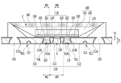
- FIG. 1 is a plan view of a light emitting device package according to an embodiment of the present invention
- FIG. 2 is a bottom view of the light emitting device package shown in FIG.
- FIG. 3 is a cross-sectional view taken along line D-D of the light emitting device package shown in FIG.
- FIGS. 4 to 11 are views illustrating a method of manufacturing a light emitting device package according to an embodiment of the present invention.
- FIG. 12 is a cross-sectional view of a light emitting device package according to an embodiment of the present invention disposed on a circuit board.
- FIG. 13 is a view showing another example of the light emitting device package according to the embodiment of the present invention.
- FIG. 14 is a plan view illustrating a light emitting device applied to a light emitting device package according to an embodiment of the present invention.
- FIG. 15 is a cross-sectional view taken along line A-A of the light emitting device shown in Fig.
- 16 is a plan view illustrating another example of a light emitting device applied to a light emitting device package according to an embodiment of the present invention.
- FIG. 17 is a cross-sectional view taken along the line F-F of the light emitting device shown in Fig.
- the semiconductor device may include various electronic devices such as a light emitting device and a light receiving device.
- the light emitting device and the light receiving device may include the first conductivity type semiconductor layer, the active layer, and the second conductivity type semiconductor layer.
- the semiconductor device according to this embodiment may be a light emitting device.
- the light emitting device emits light by recombination of electrons and holes, and the wavelength of the light is determined by the energy band gap inherent to the material. Thus, the light emitted may vary depending on the composition of the material.
- FIG. 1 is a plan view of a light emitting device package 100 according to an embodiment of the present invention
- FIG. 2 is a bottom view of the light emitting device package shown in FIG. 3 is a cross-sectional view taken along line D-D of the light emitting device package shown in FIG.
- a light emitting device package 100 may include a package body 110 and a light emitting device 120.
- the package body 110 may include a first frame 111 and a second frame 112.
- the package body 110 may include a body 113.
- the body 113 may be disposed between the first frame 111 and the second frame 112.
- the body 113 may function as an electrode separation line.
- the body 113 may be referred to as an insulating member.
- the light emitting device package 100 may include a first lower recess R11 and a second lower recess R12.
- the first lower recess R11 and the second lower recess R12 may be spaced apart from each other.
- the first lower recess R11 may be provided on a lower surface of the first frame 111. [ The first lower recess R11 may be concave in the upper surface direction of the lower surface of the first frame 111. [ The first lower recess R11 may be spaced apart from the first opening TH1.
- the second lower recess R12 may be provided on the lower surface of the second frame 112.
- the second lower recess R12 may be concave in the upper surface direction on the lower surface of the second frame 112.
- the second lower recess R12 may be spaced apart from the second opening TH2.
- the first and second conductive layers 321 and 322 may be disposed in the first opening TH1 and the second opening TH2, respectively.
- FIG. 3 is a cross-sectional view taken along line D-D of the light emitting device package shown in FIG. 1, and FIGS. 4 to 11 are views illustrating a method of manufacturing a light emitting device package according to an embodiment of the present invention.
- the light emitting device package 100 may include a package body 110 and a light emitting device 120, as shown in FIG.
- the package body 110 may include a first frame 111 and a second frame 112.
- the first frame 111 and the second frame 112 may be spaced apart from each other.
- the package body 110 may include a body 113.
- the body 113 may be disposed between the first frame 111 and the second frame 112.
- the body 113 may function as an electrode separation line.
- the body 113 may be referred to as an insulating member.
- the body 113 may be disposed on the first frame 111. In addition, the body 113 may be disposed on the second frame 112.
- the body 113 may provide an inclined surface disposed on the first frame 111 and the second frame 112.
- a cavity C may be provided on the first frame 111 and the second frame 112 by an inclined surface of the body 113.
- the package body 110 may be provided with a cavity C, or may be provided with a flat upper surface without a cavity C.
- the body 113 may be formed of a material selected from the group consisting of polyphthalamide (PPA), polychloro tri phenyl (PCT), liquid crystal polymer (LCP), polyamide 9T, silicone, epoxy molding compound, And may be formed of at least one selected from the group including silicon molding compound (SMC), ceramic, photo sensitive glass (PSG), sapphire (Al 2 O 3 ), and the like.
- the body 113 may include a high refractive index filler such as TiO 2 and SiO 2 .
- first frame 111 and the second frame 112 may be provided as a conductive frame.
- the first frame 111 and the second frame 112 can stably provide the structural strength of the package body 110 and can be electrically connected to the light emitting device 120.
- the light emitting device 120 may include a first bonding portion 121, a second bonding portion 122, a light emitting structure 123, and a substrate 124 .
- the light emitting structure 123 may include a first conductive semiconductor layer, a second conductive semiconductor layer, and an active layer disposed between the first conductive semiconductor layer and the second conductive semiconductor layer.
- the first bonding portion 121 may be electrically connected to the first conductive semiconductor layer.
- the second bonding portion 122 may be electrically connected to the second conductivity type semiconductor layer.
- the light emitting device 120 may be disposed on the package body 110.
- the light emitting device 120 may be disposed on the first frame 111 and the second frame 112.
- the light emitting device 120 may be disposed in the cavity C provided by the package body 110.
- the first bonding portion 121 may be disposed on the lower surface of the light emitting device 120.
- the second bonding portion 122 may be disposed on the lower surface of the light emitting device 120.
- the first bonding part 121 and the second bonding part 122 may be spaced apart from each other on the lower surface of the light emitting device 120.
- the first bonding part 121 may be disposed on the first frame 111.
- the second bonding portion 122 may be disposed on the second frame 112.
- the first bonding portion 121 may be disposed between the light emitting structure 123 and the first frame 111.
- the second bonding portion 122 may be disposed between the light emitting structure 123 and the second frame 112.
- the first bonding portion 121 and the second bonding portion 122 may be formed of any one selected from the group consisting of Ti, Al, Sn, In, Ir, Ta, Pd, Co, Cr, Mg, Zn, Ni, Si, At least one material or alloy selected from the group consisting of Au, Hf, Pt, Ru, Rh, ZnO, IrOx, RuOx, NiO, RuOx / ITO, Ni / IrOx / Au, Ni / IrOx / Or may be formed as a single layer or multiple layers.
- the light emitting device package 100 may include a first opening portion TH1 and a second opening portion TH2, as shown in FIGS.
- the first frame 111 may include the first opening TH1.
- the second frame 112 may include the second opening TH2.
- the first opening (TH1) may be provided in the first frame (111).
- the first opening (TH1) may be provided through the first frame (111).
- the first opening TH1 may be provided through the upper surface and the lower surface of the first frame 111 in a first direction.
- the first opening TH1 may be disposed below the first bonding portion 121 of the light emitting device 120. Referring to FIG. The first opening TH1 may be provided to overlap with the first bonding portion 121 of the light emitting device 120. [ The first opening TH1 may be provided in a manner overlapping with the first bonding portion 121 of the light emitting device 120 in a first direction toward the lower surface from the upper surface of the first frame 111. [ The first bonding portion 121 may be disposed on the first opening TH1.
- the second opening (TH2) may be provided in the second frame (112).
- the second opening (TH2) may be provided through the second frame (112).
- the second opening portion TH2 may be provided through the upper surface and the lower surface of the second frame 112 in a first direction.
- the second opening TH2 may be disposed below the second bonding portion 122 of the light emitting device 120.
- the second opening portion TH2 may be provided so as to overlap with the second bonding portion 122 of the light emitting device 120.
- the second opening portion TH2 may be provided in a manner overlapping with the second bonding portion 122 of the light emitting device 120 in a first direction toward the lower surface from the upper surface of the second frame 112.
- the second bonding portion 122 may be disposed on the second opening portion TH2.
- the first opening TH1 and the second opening TH2 may be spaced apart from each other.
- the first opening portion TH1 and the second opening portion TH2 may be spaced apart from each other below the lower surface of the light emitting device 120.
- the width W1 of the upper region of the first opening TH1 may be less than or equal to the width of the first bonding portion 121.
- the width of the upper region of the second opening portion TH2 may be less than or equal to the width of the second bonding portion 122.
- first bonding portion 121 of the light emitting device 120 and the first frame 111 can be more firmly attached.
- second bonding portion 122 of the light emitting device 120 and the second frame 112 can be more firmly attached.
- the width W1 of the upper region of the first opening TH1 may be less than or equal to the width W2 of the lower region of the first opening TH1.
- the width of the upper area of the second opening TH2 may be smaller than or equal to the width of the lower area of the second opening TH2.
- the first opening TH1 may include an upper region disposed adjacent to an upper surface of the first frame 111 and a lower region disposed adjacent to a lower surface of the first frame 111.
- the periphery of the upper region of the first opening TH1 may be smaller than the periphery of the lower region of the first opening TH1.
- the first opening (TH1) includes a first point having a smallest circumference in a first direction, and the first point is located at a position closer to the lower region of the first opening (TH1) with respect to a direction perpendicular to the first direction And may be disposed closer to the upper region of the first opening TH1.
- the second opening portion TH2 may include an upper region disposed adjacent to an upper surface of the second frame 112 and a lower region disposed adjacent to a lower surface of the second frame 112. [
- the upper area of the second opening TH2 may be smaller than the lower area of the second opening TH2.
- the second opening (TH2) includes a first point having a smallest circumference in a first direction, and the first point is positioned at a position lower than the lower area of the second opening (TH2) with respect to a direction perpendicular to the first direction And may be disposed closer to the upper region of the second opening TH2.
- the first and second lead frames 111 and 112 are etched in the top surface direction and the bottom surface direction Respectively.
- the first and second openings TH1 and TH2 may be provided in the form of a snowman as the etching proceeds in the top and bottom directions of the first and second lead frames 111 and 112 .
- the widths of the first and second openings TH1 and TH2 may gradually increase from the lower region to the middle region and then decrease again.
- the width may gradually increase from the reduced width intermediate region to the upper region, and then decrease again.
- the first point of the first and second openings TH1 and TH2 described above may refer to a boundary region in which the size of the opening in the snowman shape decreases from the lower region to the upper region and then increases again.
- the first and second openings TH1 and TH2 are formed in a first region disposed on the upper surface of each of the first and second frames 111 and 112 and a second region disposed on the lower surface of the first and second frames 111 and 112, And a second region disposed in the second region.
- the width of the upper surface of the first region may be smaller than the width of the lower surface of the second region.
- the first and second frames 111 and 112 may include a supporting member and first and second metal layers 111a and 112a surrounding the supporting member.
- a plating process or the like for the supporting members constituting the first and second frames 111 and 112 may be formed. Accordingly, the first and second metal layers 111a and 112a may be formed on the surfaces of the support members constituting the first and second frames 111 and 112.
- the first and second metal layers 111a and 112a may be provided on the upper and lower surfaces of the first and second frames 111 and 112, respectively. Also, the first and second metal layers 111a and 112a may be provided in a boundary region in contact with the first and second openings TH1 and TH2.
- the first and second metal layers 111a and 112a provided in the boundary region in contact with the first and second openings TH1 and TH2 are formed in the first and second openings TH1 and TH2, And the first and second alloy layers 111b and 112b may be combined with the first and second conductive layers 321 and 322, respectively.
- the formation of the first and second alloy layers 111b and 112b will be described later.
- first and second frames 111 and 112 may be provided as a Cu layer as a basic supporting member.
- first and second metal layers 111a and 112a may include at least one of a Ni layer, an Ag layer, and the like.
- the Ni layer has a small change in thermal expansion, so that even when the size or placement of the package body is changed due to thermal expansion, The position of the light emitting element disposed on the upper portion can be stably fixed by the Ni layer.
- the first and second metal layers 111a and 112a include an Ag layer, the Ag layer can efficiently reflect light emitted from the light emitting device disposed on the upper side and improve the brightness.
- the width of the first bonding portion 121 may be greater than or equal to the width of the first bonding portion 121.
- the width of the upper region of the second opening portion TH2 may be greater than or equal to the width of the second bonding portion 122.
- the width of the upper region of the first opening TH1 may be less than or equal to the width of the lower region of the first opening TH1.
- the width of the upper area of the second opening TH2 may be smaller than or equal to the width of the lower area of the second opening TH2.
- the width of the upper region of the first opening TH1 may be from several tens of micrometers to several hundreds of micrometers.
- the width of the lower region of the first opening TH1 may be several tens of micrometers to several hundreds of micrometers larger than the width of the upper region of the first opening TH1.
- the width of the upper region of the second opening portion TH2 may be several tens of micrometers to several hundreds of micrometers.
- the width of the lower region of the second opening TH2 may be several tens of micrometers to several hundreds of micrometers larger than the width of the upper region of the second opening TH2.
- the width W3 between the first opening TH1 and the second opening TH2 in the lower surface region of the first frame 111 and the second frame 112 may be several hundred micrometers.
- the width W3 between the first opening portion TH1 and the second opening portion TH2 in the lower surface region of the first frame 111 and the second frame portion 112 is set to be, for example, 100 micrometers to 150 micrometers Lt; / RTI >
- the width W3 between the first opening portion TH1 and the second opening portion TH2 in the lower surface region of the first frame 111 and the second frame 112 is set to be larger than the width W3 of the light emitting device package 100 may be selected to be provided over a certain distance in order to prevent electric short between the pads when they are mounted on a circuit board, a submount, or the like.
- the light emitting device package 100 may include a first resin layer 130.
- the first resin layer 130 may be disposed between the body 113 and the light emitting device 120.
- the first resin layer 130 may be disposed between the upper surface of the body 113 and the lower surface of the light emitting device 120.
- the light emitting device package 100 may include a recess R as shown in FIGS. 3 and 4.
- the recesses R may be provided in the body 113.
- the recess R may be provided between the first opening TH1 and the second opening TH2.
- the recess (R) may be recessed in a downward direction from an upper surface of the body (113).
- the recess R may be disposed below the light emitting device 120.
- the recess R may be provided to overlap with the light emitting device 120 in the first direction.
- the first resin layer 130 may be disposed in the recess R.
- the first resin layer 130 may be disposed between the light emitting device 120 and the body 113.
- the first resin layer 130 may be disposed between the first bonding part 121 and the second bonding part 122.
- the first resin layer 130 may be disposed in contact with a side surface of the first bonding portion 121 and a side surface of the second bonding portion 122.
- the first resin layer 130 may provide a stable fixing force between the light emitting device 120 and the package body 110.
- the first resin layer 130 may provide a stable fixing force between the light emitting device 120 and the body 113.
- the first resin layer 130 may be disposed in direct contact with the upper surface of the body 113, for example.
- the first resin layer 130 may be disposed in direct contact with the lower surface of the light emitting device 120.
- the first resin layer 130 may include at least one of an epoxy-based material, a silicone-based material, a hybrid material including an epoxy-based material and a silicon-based material can do.
- the adhesive may include white silicone.
- the first resin layer 130 may provide a stable clamping force between the body 113 and the light emitting device 120 and may prevent the light emitting device 120 ) And the body 113. In this case, When the light is emitted from the light emitting device 120 to the lower surface of the light emitting device 120, the first resin layer 130 provides a light diffusion function to improve the light extraction efficiency of the light emitting device package 100 . In addition, the first resin layer 130 may reflect light emitted from the light emitting device 120. When the first resin layer 130 includes a reflection function, the first resin layer 130 may be formed of a material including TiO 2 , SiO 2 , and the like.
- the depth T1 of the recess R may be smaller than the depth T2 of the first opening TH1 or the depth T2 of the second opening TH2.
- the depth T1 of the recess R may be determined in consideration of the adhesion of the first resin layer 130.
- the depth T1 of the recess R may be determined by taking into consideration the stable strength of the body 113 and / or by applying heat to the light emitting device package 100 by heat emitted from the light emitting device 120. [ Can be determined not to occur.
- the recess R may provide a suitable space under which an under-fill process may be performed under the light emitting device 120.
- the underfilling process may be a process of mounting the light emitting device 120 on the package body 110 and then disposing the first resin layer 130 under the light emitting device 120,
- the first resin layer 130 may be disposed in the recess R for mounting through the first resin layer 130 in the process of mounting the light emitting device 120 on the package body 110, (120).
- the recess R may be provided at a depth greater than the first depth so that the first resin layer 130 may be sufficiently provided between the lower surface of the light emitting device 120 and the upper surface of the body 113.
- the recesses R may be provided at a second depth or less to provide stable strength of the body 113.
- the depth (T1) and the width (W4) of the recess (R) may affect the forming position and fixing force of the first resin layer (130).
- the depth T1 and the width W4 of the recess R are set so that sufficient fixing force can be provided by the first resin layer 130 disposed between the body 113 and the light emitting device 120 Can be determined.
- the depth (T1) of the recess (R) may be provided by several tens of micrometers.
- the depth (T1) of the recess (R) may be provided from 40 micrometers to 60 micrometers.
- the width W4 of the recess R may be several tens of micrometers to several hundreds of micrometers.
- the width W4 of the recess R may be provided in the major axis direction of the light emitting device 120.
- the width W4 of the recess R may be narrower than the gap between the first bonding portion 121 and the second bonding portion 122.
- the width W4 of the recess R may be provided in the range of 140 micrometers to 160 micrometers.
- the width W4 of the recess R may be provided at 150 micrometers.
- the depth T2 of the first opening TH1 may be provided corresponding to the thickness of the first frame 111. [ The depth T2 of the first opening TH1 may be provided to a thickness sufficient to maintain a stable strength of the first frame 111. [
- the depth T2 of the second opening portion TH2 may be provided corresponding to the thickness of the second frame 112. [ The depth T2 of the second opening portion TH2 may be provided to a thickness that can maintain stable strength of the second frame 112.
- the depth T2 of the first opening TH1 and the depth T2 of the second opening TH2 may be provided corresponding to the thickness of the body 113. [ The depth T2 of the first opening portion TH1 and the depth T2 of the second opening portion TH2 may be provided to maintain a stable strength of the body 113. [
- the depth T2 of the first opening TH1 may be several hundred micrometers.
- the depth T2 of the first opening TH1 may be 180 to 220 micrometers.
- the depth T2 of the first opening TH1 may be 200 micrometers.
- the thickness of (T2-T1) may be selected to be at least 100 micrometers or more. This is in consideration of the thickness of the injection process capable of providing crack free of the body 113.
- the ratio of the T1 thickness to the T2 thickness may be 2 to 10.
- the thickness of T2 may be provided from 20 micrometers to 100 micrometers.
- the light emitting device package 100 may include a light transmitting resin layer 160 and a reflective resin layer 170, as shown in FIGS. 3, 6 and 8.
- the light transmitting resin layer 160 may include a first light transmitting resin layer 162 disposed between the light emitting element 120 and a phosphor layer 180 formed later Accordingly, the phosphor layer 180 and the light emitting device 120 are spaced apart from each other to prevent deterioration of the phosphor layer.
- the light transmissive resin layer 160 may include a reflective resin layer 170 to be formed later and a second transmissive resin layer 161 disposed between the light emitting device 120.
- the second translucent resin layer 161 may be uniformly disposed on a side surface of the light emitting device 120.
- the light transmitting resin layer 160 may be a light transmitting material and may include light diffusing particles.
- the light transmitting resin layer 160 may include at least one of an epoxy-based material, a silicone-based material, a hybrid material including an epoxy-based material and a silicon-based material can do.
- the light transmitting resin layer 160 may include a clear series silicone or a silicone containing light diffusion particles such as ZrO 2 , ZnO, Al 2 O 3, etc. have.
- the reflective layer when the reflective layer is disposed on the light emitting device package in the prior art, when the surface of the light emitting device has hydrophilicity, the reflective layer may be widely diffused on the surface of the light emitting device.
- the efficiency with which the light emitted by the light emitting device is extracted from the light emitting device package may be degraded by the reflective layer widely disposed on the surface of the light emitting device.
- the light transmitting resin layer 160 may be disposed and cured to cure the reflective resin layer 170, It is possible to prevent the light from diffusing widely on the surface of the device, thereby improving the light extraction efficiency of the light emitting device package.
- 7A is a process sectional view of forming a light-transmitting resin on a light-emitting element in the embodiment.
- the light emitting device 120 is disposed on the supporting substrate 190. Then, a light transmitting resin layer 160 is formed on the light emitting device 120.
- the light transmitting resin layer 160 may be formed by a molding or a dotting process.
- the translucent resin layer 160 may include at least one of an epoxy-based material, a silicone-based material, a hybrid material including an epoxy-based material and a silicon-based material.
- the light transmitting resin layer 160 may include a clear series silicone or a silicone containing light diffusion particles such as ZrO 2 , ZnO, Al 2 O 3, etc. have.
- 7B is a photograph of the light emitting device 120 having the light transmitting resin layer 160 formed thereon.
- the light transmitting resin layer 160 can be uniformly formed on the side of the light emitting element,
- the width of the upper portion of the translucent resin layer 160 can be ensured to be larger than the width of the lower portion and the side surface of the translucent resin layer 160 can be formed flat without the roughness, There is a peculiar effect of forming the optical cavity described later.
- the embodiment may include a reflective resin layer 170.
- the reflective resin layer 170 may include the light emitting device 120 and a first reflective resin layer 170 disposed on a side surface of the cavity C.
- the embodiment may include a second reflective resin (not shown) disposed between the first and second bonding portions of the light emitting device 120 and the body 113, but the present invention is not limited thereto.
- the reflective resin layer 170 may include a white silicone.
- the antireflective resin layer 170 may be made of silicon including TiO 2 , ZnO, Al 2 O 3 , BN, and the like, but is not limited thereto.
- the reflective resin layer 170 may proceed from the upper side of the cavity C to the tapping process. Alternatively, the reflective resin layer 170 may be formed through a lower gap filling process through the first opening TH1 or the second opening TH2 formed in the frame. Alternatively, the reflective resin layer 170 may be formed by simultaneously performing an upper side capping process and a lower side capping process.
- the reflective resin layer 170 may be formed in a shape of a truncated cone in the light emitting device to diffusely reflect the light, thereby realizing a light cavity, thereby significantly improving the brightness of the light. .
- the prior art has a difficulty in implementing a technique of separating the light reflecting resin from the light emitting element by a predetermined distance.
- the light-transmissive resin layer 160 is disposed on the side surface of the light-emitting device so as to have a uniform side surface, so that the light-reflective resin layer 170 is uniformly spaced from the light- have.
- Fig. 9 is a process diagram showing the formation of the phosphor layer 180 in the embodiment.
- the phosphor layer 180 may include wavelength conversion means for receiving light emitted from the light emitting device 120 and providing wavelength-converted light.
- the phosphor layer 180 may include at least one selected from the group including phosphors, quantum dots, and the like.
- the reflective resin layer 170 is disposed in a shape of a cone cut in the light emitting device, and the diffusing reflection is very effectively realized through the organic bonding with the remote fluorescent layer 180 By implementing a light cavity, the brightness of the light can be significantly improved.
- the light emitting device package 100 may include a first conductive layer 321 and a second conductive layer 322, as shown in FIGS. 3 and 10.
- the first conductive layer 321 may be spaced apart from the second conductive layer 322.
- the first conductive layer 321 may be provided in the first opening TH1.
- the first conductive layer 321 may be disposed below the first bonding portion 121.
- the width of the first conductive layer 321 may be smaller than the width of the first bonding portion 121.
- the first bonding portion 121 may have a width in a second direction perpendicular to the first direction in which the first opening portion TH1 is formed.
- the width of the first bonding portion 121 may be greater than the width of the first opening TH1 in the second direction.
- the first conductive layer 321 may be disposed in direct contact with the lower surface of the first bonding portion 121.
- the first conductive layer 321 may be electrically connected to the first bonding portion 121.
- the first conductive layer 321 may be surrounded by the first frame 111.
- the lower surface of the first conductive layer 321 may be arranged in a concave shape from the lower side to the upper side.
- the second conductive layer 322 may be provided in the second opening TH2.
- the second conductive layer 322 may be disposed under the second bonding portion 122.
- the width of the second conductive layer 322 may be smaller than the width of the second bonding portion 122.
- the second bonding portion 122 may have a width in a second direction perpendicular to the first direction in which the second opening portion TH2 is formed.
- the width of the second bonding portion 122 may be greater than the width of the second opening TH2 in the second direction.
- the second conductive layer 322 may be disposed in direct contact with the lower surface of the second bonding portion 122.
- the second conductive layer 322 may be electrically connected to the second bonding portion 122.
- the second conductive layer 322 may be disposed so as to be surrounded by the second frame 112.
- the lower surface of the second conductive layer 322 may be arranged in a concave shape from the lower part to the upper part.
- the first conductive layer 321 and the second conductive layer 322 may include one selected from the group consisting of Ag, Au, Pt, Sn, Cu, and the like, or an alloy thereof. However, the present invention is not limited thereto, and the first conductive layer 321 and the second conductive layer 322 may be formed of a material capable of ensuring a conductive function.
- the first conductive layer 321 and the second conductive layer 322 may be formed using a conductive paste.
- the conductive paste may include a solder paste, a silver paste, or the like, and may be composed of a multi-layer or an alloy composed of different materials or a single layer.
- the first conductive layer 321 and the second conductive layer 322 may include a SAC (Sn-Ag-Cu) material.
- An intermetallic compound (IMC) layer may be formed between the first and second layers 111 and 112 and the layers 321 and 322.
- the material of the first and second conductive layers 321 and 322 and the first and second metal layers 111a and 112a of the first and second frames 111 and 112, And second alloy layers 111b and 112b may be formed.
- the first conductive layer 321 and the first frame 111 can be physically and electrically coupled with each other in a stable manner.
- the first conductive layer 321, the first alloy layer 111b, and the first frame 111 can be physically and electrically coupled to each other in a stable manner.
- the second conductive layer 322 and the second frame 112 can be physically and electrically coupled to each other in a stable manner.
- the second conductive layer 322, the second alloy layer 212b, and the second frame 112 can be physically and electrically coupled to each other in a stable manner.
- the first and second alloy layers 111b and 112b may include at least one intermetallic compound layer selected from the group including AgSn, CuSn, AuSn, and the like.
- the intermetallic compound layer may be formed by a combination of a first material and a second material, and a first material may be provided from the first and second conductive layers 321 and 322, And the second metal layers 111a and 112a or the supporting members of the first and second frames 111 and 112.
- an intermetallic compound layer of AgSn may be formed by a combination of a Sn material and an Ag material.
- the first and second conductive layers 321 and 322 include a Sn material and the first and second metal layers 111a and 112a include an Au material
- the intermetallic compound layer of AuSn may be formed by the combination of the Sn material and the Au material in the process of providing the electrode material 321 or 322 or in the heat treatment process after being provided.
- the intermetallic compound layer of CuSn can be formed by the combination of the Sn material and the Cu material in the process of providing the conductive layers 321 and 322 or in the heat treatment process after being provided.
- the first and second conductive layers 321 and 322 include Ag material and the first and second metal layers 111a and 111b or the supporting members of the first and second frames 111 and 112 Sn material, the intermetallic compound layer of AgSn may be formed by the bonding of the Ag material and the Sn material in the process of providing the first and second conductive layers 321 and 322 or in the heat treatment process after being provided.
- the intermetallic compound layer described above can have a higher melting point than a general bonding material.
- the heat treatment process in which the metal compound layer is formed can be performed at a lower temperature than the melting point of a general bonding material.
- the package body 110 does not need to be exposed to high temperatures in the process of manufacturing the light emitting device package. Therefore, according to the embodiment, it is possible to prevent the package body 110 from being exposed to high temperatures to be damaged or discolored.
- the selection range for the material constituting the body 113 can be widened.
- the body 113 may be provided using not only expensive materials such as ceramics but also relatively inexpensive resin materials.
- the body 113 may include at least one material selected from the group consisting of PPA (PolyPhtalAmide) resin, PCT (PolyCyclohexylenedimethylene Terephthalate) resin, EMC (Epoxy Molding Compound) resin and SMC can do.
- PPA PolyPhtalAmide
- PCT PolyCyclohexylenedimethylene Terephthalate
- EMC Epoxy Molding Compound
- an intermetallic compound layer may also be formed between the first and second bonding portions 121 and 122 and the first and second conductive layers 321 and 322.
- An intermetallic compound (IMC) layer may be formed between the first and second conductive layers 321 and 322 and the first and second bonding portions 121 and 122.
- an alloy layer may be formed by bonding between the first and second conductive layers 321 and 322 and the first and second bonding portions 121 and 122.
- the first conductive layer 321 and the first bonding portion 121 can be physically and electrically coupled more stably.
- the first conductive layer 321, the alloy layer, and the first bonding portion 121 can be physically and electrically coupled stably.
- the second conductive layer 322 and the second bonding portion 122 can be physically and electrically coupled more stably.
- the second conductive layer 322, the alloy layer, and the second bonding portion 122 can be physically and electrically coupled stably.
- the alloy layer may include at least one intermetallic compound layer selected from the group including AgSn, CuSn, AuSn, and the like.
- the intermetallic compound layer may be formed by a combination of a first material and a second material, and a first material may be provided from the first and second conductive layers 321 and 322, And the second bonding portions 121 and 122, respectively.
- the first and second conductive layers 321 and 322 include a Sn material and the first and second bonding portions 121 and 122 include an Ag material
- the first and second conductive layers 321 and 322 , 322 are provided, or an intermetallic compound layer of AgSn can be formed by the bonding of the Sn material and the Ag material in the heat treatment process after being provided.
- the intermetallic compound layer of AuSn may be formed by the combination of the Sn material and the Au material during the process of providing the first and second electrodes 321 and 322 or after the heat treatment.
- the intermetallic compound layer of AgSn may be formed by the bonding of the Ag material and the Sn material in the process of providing the first and second conductive layers 321 and 322 or in the heat treatment process after being provided.
- the intermetallic compound layer described above can have a higher melting point than a general bonding material.
- the heat treatment process in which the metal compound layer is formed can be performed at a lower temperature than the melting point of a general bonding material.
- the light emitting device package 100 may include a first lower recess R11 and a second lower recess R12, as shown in FIGS. 3 and 10.
- the first lower recess R11 and the second lower recess R12 may be spaced apart from each other.
- the first lower recess R11 may be provided on a lower surface of the first frame 111. [ The first lower recess R11 may be concave in the upper surface direction of the lower surface of the first frame 111. [ The first lower recess R11 may be spaced apart from the first opening TH1.
- the first lower recess R11 may be provided with a width of several micrometers to several tens of micrometers.
- a resin part may be provided in the first lower recess R11.
- the resin part filled in the first lower recess R11 may be provided with the same material as the body 113, for example.
- the present invention is not limited thereto, and the resin part may be selected from materials having poor adhesive force and wettability with the first and second conductive layers 321 and 322.
- the resin portion may be selected and provided from a material having a low surface tension with respect to the first and second conductive layers 321 and 322.
- the resin part filled in the first lower recess R11 may be provided in the process of forming the first frame 111, the second frame 112, and the body 113 through an injection process or the like .
- the resin portion filled in the first lower recess R11 may be disposed around the lower surface region of the first frame 111 providing the first opening TH1.
- the lower surface of the first frame 111 providing the first opening TH1 may be disposed in a shape of an island in a state separated from a lower surface of the first frame 111 surrounding the first frame 111.
- the lower surface of the first frame 111 providing the first opening TH1 is divided into a resin portion filled in the first lower recess R11 and a lower portion of the body 113
- the second frame 111 may be isolated from the surrounding first frame 111.
- the resin part may be formed of a material having poor adhesion to the first and second conductive layers 321 and 322, a poor wettability, or a material having a low surface tension between the resin part and the first and second conductive layers 321 and 322
- the first conductive layer 321 provided in the first opening TH1 is displaced from the first opening TH1 and the resin portion filled in the first lower recess R11 or the body 113, Can be prevented from spreading beyond.
- the material of the first conductive layer 321 may be selected to have a good adhesion property with the first frame 111.
- the material of the first conductive layer 321 may be selected to have poor adhesion properties with the resin and the body 113.
- the first conductive layer 321 may flow over the first opening TH1 in the direction of the region where the resin or the body 113 is provided so that the resin or the body 113 And the first conductive layer 321 can be stably disposed in the region provided with the first opening TH1.
- the first conductive layer 321 disposed in the first opening TH1 overflows, the first conductive layer 321 is electrically connected to an outer region of the first lower recess R11 provided with the resin or the body 113, The conductive layer 321 can be prevented from expanding. Also, the first conductive layer 321 can be stably connected to the lower surface of the first bonding portion 121 in the first opening TH1.
- the first conductive layer 321 and the second conductive layer 322 can be prevented from being in contact with each other to be short-circuited, and the first and second conductive layers 321 and 322 can be controlled, the amount of the first and second conductive layers 321 and 322 can be very easily controlled.
- the second lower recess R12 may be provided on the lower surface of the second frame 112.
- the second lower recess R12 may be concave in the upper surface direction on the lower surface of the second frame 112.
- the second lower recess R12 may be spaced apart from the second opening TH2.
- the second lower recess R12 may be provided with a width of several micrometers to tens of micrometers.
- a resin part may be provided in the second lower recess R12.
- the resin part filled in the second lower recess R12 may be provided with the same material as the body 113, for example.
- the present invention is not limited thereto, and the resin part may be selected from materials having poor adhesive force and wettability with the first and second conductive layers 321 and 322.
- the resin portion may be selected and provided from a material having a low surface tension with respect to the first and second conductive layers 321 and 322.
- a resin part filled in the second lower recess R12 may be provided in the process of forming the first frame 111, the second frame 112, and the body 113 through an injection process or the like .
- a resin portion filled in the second lower recess R12 may be disposed around a lower surface region of the second frame 112 providing the second opening TH2.
- the lower surface of the second frame 112 providing the second opening TH2 may be disposed in a form of an island in a shape separated from the lower surface of the second frame 112 surrounding the second frame 112.
- the lower surface of the second frame 112, which provides the second opening TH2 has a resin part filled in the second lower recess R12 and a lower surface of the body 113 May be isolated from the second frame 112 in the vicinity.
- the resin part may be formed of a material having poor adhesion to the first and second conductive layers 321 and 322, a poor wettability, or a material having a low surface tension between the resin part and the first and second conductive layers 321 and 322
- the second conductive layer 322 provided in the second opening TH2 may be displaced from the second opening TH2 so that the resin portion or the body 113 filled in the second lower recess R12 may be removed, Can be prevented from spreading beyond.
- the material of the second conductive layer 322 may be selected to have good adhesion properties with the second frame 112.
- the material constituting the second conductive layer 322 may be selected to have poor adhesion properties with the resin part and the body 113.
- the second conductive layer 322 overflows from the second opening TH2 in the direction of the region where the resin or the body 113 is provided so that the resin or the body 113 And the second conductive layer 322 can be stably disposed in the region where the second opening portion TH2 is provided.
- the second conductive layer 322 disposed in the second opening TH2 overflows, the second conductive layer 322 is electrically connected to an outer region of the second lower recess R12 provided with the resin portion or the body 113, The conductive layer 322 can be prevented from expanding. In addition, the second conductive layer 322 can be stably connected to the lower surface of the second bonding portion 122 in the second opening portion TH2.
- the first conductive layer 321 and the second conductive layer 322 can be prevented from being in contact with each other to be short-circuited, and the first and second conductive layers 321 and 322 can be controlled, the amount of the first and second conductive layers 321 and 322 can be very easily controlled.
- the first resin layer 130 provided on the recess R may be formed on the lower surface of the light emitting device 120. In this case, And the upper surface of the package body 110. [0035] The first resin layer 130 may be provided around the first and second bonding portions 121 and 122 when viewed from the upper direction of the light emitting device 120. The first resin layer 130 may be provided around the first and second openings TH1 and TH2 when viewed from above the light emitting device 120. [
- the first resin layer 130 may function to stably fix the light emitting device 120 to the package body 110.
- the first resin layer 130 may be disposed around the first and second bonding portions 121 and 122 in contact with the side surfaces of the first and second bonding portions 121 and 122.
- the first resin layer 130 may surround the first bonding part 121 and the second bonding part 122.
- the first resin layer 130 is formed such that the first conductive layer 321 and the second conductive layer 322 are separated from the first opening TH1 and the second opening TH2, 120 in the outer side direction.
- the first and second conductive layers 321 and 322 are diffused and moved in the outer surface direction of the light emitting device 120, the first and second conductive layers 321 and 322 are electrically connected to the active layer of the light emitting device 120 Which can lead to failure due to a short circuit. Accordingly, when the first resin layer 130 is disposed, the first and second conductive layers 321 and 322 and the active layer can be prevented from being short-circuited, thereby improving the reliability of the light emitting device package according to the embodiment.
- the first resin layer 130 may be formed such that the first conductive layer 321 and the second conductive layer 322 are separated from the first opening TH1 and the second opening TH2, Can be prevented from diffusing and moving in the recess (R) direction below the lower surface of the element 120. [ Accordingly, the first conductive layer 321 and the second conductive layer 322 can be prevented from being electrically short-circuited under the light emitting device 120.
- the light emitting structure 123 may be provided as a compound semiconductor.
- the light emitting structure 123 may be formed of, for example, a Group 2-VI-VI or Group III-V compound semiconductor.
- the light emitting structure 123 may include at least two elements selected from aluminum (Al), gallium (Ga), indium (In), phosphorus (P), arsenic (As) .
- the light emitting structure 123 may include a first conductive semiconductor layer, an active layer, and a second conductive semiconductor layer.
- power is connected to the first bonding portion 121 through the first opening portion TH1, and power is supplied to the second bonding portion 121 through the second opening portion TH2. (Not shown).
- the light emitting device 120 can be driven by the driving power supplied through the first bonding part 121 and the second bonding part 122.
- the light emitted from the light emitting device 120 may be provided in an upward direction of the package body 110.
- the light emitting device package 100 may be mounted on a submount, a circuit board, or the like.
- a high temperature process such as a reflow process can be applied.
- a re-melting phenomenon occurs in the bonding region between the lead frame and the light emitting device provided in the light emitting device package, so that the stability of electrical connection and physical coupling can be weakened.
- the bonding portion of the light emitting device according to the embodiment can receive the driving power through the conductive layer disposed in the opening portion.
- the melting point of the conductive layer disposed in the opening and the melting point of the intermetallic compound layer may be selected to have a higher value than the melting point of the common bonding material.
- the package body 110 does not need to be exposed to high temperatures in the process of manufacturing the light emitting device package. Therefore, according to the embodiment, it is possible to prevent the package body 110 from being exposed to high temperatures to be damaged or discolored.
- the selection range for the material constituting the body 113 can be widened.
- the body 113 may be provided using not only expensive materials such as ceramics but also relatively inexpensive resin materials.
- the body 113 may include at least one material selected from the group consisting of PPA (PolyPhtalAmide) resin, PCT (PolyCyclohexylenedimethylene Terephthalate) resin, EMC (Epoxy Molding Compound) resin and SMC can do.
- PPA PolyPhtalAmide
- PCT PolyCyclohexylenedimethylene Terephthalate
- EMC Epoxy Molding Compound
- the embodiment may include a second resin layer 115 disposed in the first and second openings TH1 and TH2.
- the second resin layer 115 may be disposed under the first and second conductive layers 321 and 322.
- the second resin layer 115 may protect the first and second conductive layers 321 and 322.
- the second resin layer 115 may seal the first and second openings TH1 and TH2.
- the second resin layer 115 may prevent the first and second conductive layers 321 and 322 from diffusing and moving under the first and second openings TH1 and TH2.
- the second resin layer 115 may include a material similar to the body 113.
- the second resin layer 115 may include at least one material selected from the group consisting of PPA (PolyPhtalAmide) resin, PCT (PolyCyclohexylenedimethylene Terephthalate) resin, EMC (Epoxy Molding Compound) resin and SMC .
- the second resin layer 115 may include at least one of an epoxy-based material, a silicone-based material, a hybrid material including an epoxy-based material and a silicon-based material .
- the light emitting device package according to the embodiment of the present invention is another example in which the light emitting device package described with reference to FIGS. 1 to 11 is mounted on the circuit board 410 and supplied.
- the light emitting device package may include a circuit board 410, a package body 110, and a light emitting device 120, as shown in FIG.
- the circuit board 410 may include a first pad 411, a second pad 412, and a substrate 413.
- the substrate 413 may be provided with a power supply circuit for controlling the driving of the light emitting device 120.
- the package body 110 may be disposed on the circuit board 410.
- the first pad 411 and the first bonding portion 121 may be electrically connected to each other.
- the second pad 412 and the second bonding portion 122 may be electrically connected to each other.
- the first pad 411 and the second pad 412 may include a conductive material.
- the first pad 411 and the second pad 412 may be formed of a material selected from the group consisting of Ti, Cu, Ni, Au, Cr, Ta, Pt, Sn, Ag, P, Fe, At least one selected material or alloy thereof.
- the first pad 411 and the second pad 412 may be provided as a single layer or a multilayer.
- the package body 110 may include a first frame 111 and a second frame 112.
- the first frame 111 and the second frame 112 may be spaced apart from each other.
- the package body 110 may include a body 113.
- the body 113 may be disposed between the first frame 111 and the second frame 112.
- the body 113 may function as an electrode separation line.
- the first frame 111 and the second frame 112 may be provided as a conductive frame.
- the first frame 111 and the second frame 112 can stably provide the structural strength of the package body 110 and can be electrically connected to the light emitting device 120.
- FIG. 13 is a view showing another example of the light emitting device package according to the embodiment of the present invention.
- the light emitting device package according to the embodiment shown in FIG. 13 may further include a heat dissipating member 150 as compared with the light emitting device package according to the embodiment shown in FIG.
- the heat dissipating member 150 may be disposed in a third portion (not shown) provided in the body 113 and may be disposed below the recess R.
- the radiation member 230 may be disposed between the first frame 111 and the second frame 112.
- the heat dissipation member 150 may include at least one of an epoxy-based material, a silicone-based material, a hybrid material including an epoxy-based material and a silicon-based material have. Also, for example, when the heat radiating member 150 includes a reflection function, the heat radiating member 150 may include white silicone.
- the heat dissipation member 150 may include a material selected from the group consisting of Al 2 O 3 , AlN, and the like having good thermal conductivity.
- the heat dissipating member 150 when the heat dissipating member 150 includes a material having a good thermal conductivity, heat generated from the light emitting device 120 can be effectively dissipated. Accordingly, since the heat emission of the light emitting device 120 can be effectively performed, the light extraction efficiency of the light emitting device 120 can be improved.
- the heat dissipating member 150 includes a reflective material
- a light diffusion function is provided between the light emitting device 120 and the body 113 with respect to light emitted to the lower surface of the light emitting device 120 can do.
- the heat dissipating member 230 may improve the light extraction efficiency of the light emitting device package by providing a light diffusion function.
- the radiation member 150 may reflect light emitted from the light emitting device 120.
- the heat dissipation member 150 includes a reflection function
- the heat dissipation member 230 may be formed of a material including TiO 2 , SiO 2 , and the like.
- FIG. 14 is a plan view showing a light emitting device according to an embodiment of the present invention
- FIG. 15 is a sectional view taken along line A-A of the light emitting device shown in FIG.
- the first sub-electrode 2171 and the second sub-electrode 2172 are disposed under the first bonding portion 2171 and the second bonding portion 2172 and are electrically connected to the first bonding portion 2171.
- a second sub electrode 2142 electrically connected to the second bonding portion 2172 can be seen.
- the light emitting device 2100 may include the light emitting structure 1110 disposed on the substrate 2105, as shown in FIGS. 14 and 15.
- FIG. 14 and 15 The light emitting device 2100 according to the embodiment may include the light emitting structure 1110 disposed on the substrate 2105, as shown in FIGS. 14 and 15.
- FIG. 14 and 15 FIG. 14
- the substrate 2105 may be selected from the group including a sapphire substrate (Al 2 O 3 ), SiC, GaAs, GaN, ZnO, Si, GaP, InP and Ge.
- the substrate 2105 may be provided as a patterned sapphire substrate (PSS) having a concavo-convex pattern formed on its upper surface.
- PSS patterned sapphire substrate
- the light emitting structure 1110 may include a first conductive semiconductor layer 1111, an active layer 1112, and a second conductive semiconductor layer 1113.
- the active layer 1112 may be disposed between the first conductive semiconductor layer 1111 and the second conductive semiconductor layer 1113.
- the active layer 1112 may be disposed on the first conductive semiconductor layer 1111, and the second conductive semiconductor layer 1113 may be disposed on the active layer 1112.
- the first conductivity type semiconductor layer 1111 may be provided as an n-type semiconductor layer, and the second conductivity type semiconductor layer 1113 may be provided as a p-type semiconductor layer.
- the first conductivity type semiconductor layer 1111 may be provided as a p-type semiconductor layer, and the second conductivity type semiconductor layer 1113 may be provided as an n-type semiconductor layer.
- the first conductive semiconductor layer 1111 is provided as an n-type semiconductor layer and the second conductive semiconductor layer 1113 is provided as a p-type semiconductor layer for convenience of description .
- the light emitting device 2100 may include a light transmitting electrode layer 2130 as shown in FIG.
- the light transmitting electrode layer 2130 can increase the light output by increasing the current diffusion.
- the light transmitting electrode layer 2130 may include at least one selected from the group consisting of a metal, a metal oxide, and a metal nitride.
- the transmissive electrode layer 2130 may include a light-transmitting material.
- the transmissive electrode layer 2130 may be formed of a material such as ITO (indium tin oxide), IZO (indium zinc oxide), IZON (indium zinc oxide), IZTO (indium zinc tin oxide), IAZO gallium zinc oxide (IGTO), aluminum zinc oxide (AZO), antimony tin oxide (ATO), gallium zinc oxide (GZO), IrOx, RuOx, RuOx / ITO, Ni / IrOx / IrOx / Au / ITO, Pt, Ni, Au, Rh, and Pd.
- ITO indium tin oxide
- IZO indium zinc oxide
- IZON indium zinc oxide
- IZTO indium zinc tin oxide
- AZO aluminum zinc oxide
- ATO antimony tin oxide
- GZO gallium zinc oxide
- the light emitting device 2100 may include a reflective layer 2160, as shown in FIGS.
- the reflective layer 2160 may include a first reflective layer 2161, a second reflective layer 2162, and a third reflective layer 2163.
- the reflective layer 2160 may be disposed on the transmissive electrode layer 2130.
- the second reflective layer 2162 may include a first opening h1 for exposing the transmissive electrode layer 2130.
- the second reflective layer 2162 may include a plurality of first openings h1 disposed on the transmissive electrode layer 2130.
- the first reflective layer 2161 may include a plurality of second openings h2 exposing the upper surface of the first conductive type semiconductor layer 1111.
- the third reflective layer 2163 may be disposed between the first reflective layer 2161 and the second reflective layer 2162.
- the third reflective layer 2163 may be connected to the first reflective layer 2161.
- the third reflective layer 2163 may be connected to the second reflective layer 2162.
- the third reflective layer 2163 may be physically in direct contact with the first reflective layer 2161 and the second reflective layer 2162.
- the reflective layer 2160 may be in contact with the second conductive type semiconductor layer 1113 through a plurality of contact holes provided in the transmissive electrode layer 2130. [ The reflective layer 2160 may be physically contacted to the upper surface of the second conductive type semiconductor layer 1113 through a plurality of contact holes provided in the transmissive electrode layer 2130.
- the reflective layer 2160 may be provided as an insulating reflective layer.
- the reflective layer 2160 may be provided as a DBR (Distributed Bragg Reflector) layer.
- the reflective layer 2160 may be provided as an ODR (Omni Directional Reflector) layer.
- the reflective layer 2160 may be provided by stacking a DBR layer and an ODR layer.
- the light emitting device 2100 may include a first sub electrode 2141 and a second sub electrode 2142, as shown in FIGS. 14 and 15.
- FIG. 14 and 15 The light emitting device 2100 according to the embodiment may include a first sub electrode 2141 and a second sub electrode 2142, as shown in FIGS. 14 and 15.
- FIG. 14 and 15 FIG. 14
- the first sub-electrode 2141 may be electrically connected to the first conductive type semiconductor layer 1111 in the second opening h2.
- the first sub-electrode 2141 may be disposed on the first conductive semiconductor layer 1111.
- the first sub-electrode 2141 penetrates the second conductive semiconductor layer 1113 and the active layer 1112 to form the first conductive semiconductor layer 1111.
- the first conductivity type semiconductor layer 1111 may be disposed on the upper surface of the first conductive type semiconductor layer 1111 in the recess.
- the first sub electrode 2141 may be electrically connected to the upper surface of the first conductive type semiconductor layer 1111 through a second opening h2 provided in the first reflective layer 2161. [ 24 and 25, the first sub-electrode 2141 and the second sub-electrode 2141 may overlap each other in the plurality of recessed regions, 1-conductivity type semiconductor layer 1111. [0216]
- the second sub-electrode 2142 may be electrically connected to the second conductive type semiconductor layer 1113.
- the second sub-electrode 2142 may be disposed on the second conductive type semiconductor layer 1113.
- the transparent electrode layer 2130 may be disposed between the second sub-electrode 2142 and the second conductive type semiconductor layer 1113.
- the second sub electrode 2142 may be electrically connected to the second conductive type semiconductor layer 1113 through a first opening h1 provided in the second reflective layer 2162. [ 14 and 15, the second sub-electrode 2142 is electrically connected to the second conductivity type semiconductor layer 1113 through the light-transmitting electrode layer 2130 in a plurality of P regions Can be connected.
- the second sub-electrode 2142 is electrically connected to the transmissive electrode layer 2130 through a plurality of first openings h1 provided in the second reflective layer 2162 in a plurality of P regions ). ≪ / RTI >
- the first sub-electrode 2141 and the second sub-electrode 2142 may have polarities and may be spaced apart from each other.
- the first sub-electrode 2141 may be provided in a plurality of line shapes as an example. Also, the second sub-electrodes 2142 may be provided in a plurality of line shapes as an example. The first sub-electrode 2141 may be disposed between a plurality of neighboring second sub-electrodes 2142. The second sub-electrode 2142 may be disposed between a plurality of neighboring first sub-electrodes 2141.
- first sub-electrode 2141 and the second sub-electrode 2142 may be arranged in different numbers of electrodes. For example, when the first sub-electrode 2141 is an n-electrode and the second sub-electrode 2142 is a p-electrode, the number of the second sub-electrodes 2142 is greater than the number of the second sub- Can be more.
- the first sub electrode 2141 and the second sub electrode 2142 are electrically connected to each other when the electrical conductivity and / or resistance of the second conductivity type semiconductor layer 1113 and the first conductivity type semiconductor layer 1111 are different from each other,
- the electrons injected into the light emitting structure 1110 can be balanced with the holes and thus the optical characteristics of the light emitting device can be improved.
- the polarities of the first sub-electrode 2141 and the second sub-electrode 2142 may be opposite to each other, depending on the characteristics required in the light emitting device package to which the light emitting device according to the embodiment is applied.
- the width, length, shape, and number of the first sub-electrode 2141 and the second sub-electrode 2142 can be variously modified according to characteristics required in the light emitting device package.
- the first sub-electrode 2141 and the second sub-electrode 2142 may have a single-layer structure or a multi-layer structure.
- the first sub-electrode 2141 and the second sub-electrode 2142 may be ohmic electrodes.
- the first sub-electrode 2141 and the second sub-electrode 2142 may be formed of a metal such as ZnO, IrOx, RuOx, NiO, RuOx / ITO, Ni / IrOx / Au, and Ni / IrOx / , At least one of Ni, Cr, Ti, Al, Rh, Pd, Ir, Ru, Mg, Zn, Pt, Au and Hf or an alloy of two or more of them.
- a metal such as ZnO, IrOx, RuOx, NiO, RuOx / ITO, Ni / IrOx / Au, and Ni / IrOx / , At least one of Ni, Cr, Ti, Al, Rh, Pd, Ir, Ru, Mg, Zn, Pt, Au and Hf or an alloy of two or more of them.
- the light emitting device 2100 may include a protective layer 2150, as shown in FIGS.
- the protective layer 2150 may include a plurality of third openings h3 exposing the second sub-electrodes 2142.
- the plurality of third openings h3 may be disposed corresponding to a plurality of PB regions provided in the second sub-electrode 2142.
- the protective layer 2150 may include a plurality of fourth openings h4 for exposing the first sub-electrode 2141.
- the plurality of fourth openings h4 may be disposed corresponding to a plurality of NB regions provided in the first sub-
- the protective layer 2150 may be disposed on the reflective layer 2160.
- the protective layer 2150 may be disposed on the first reflective layer 2161, the second reflective layer 2162, and the third reflective layer 2163.
- the protective layer 2150 may be provided as an insulating material.
- the passivation layer 2150 may include at least one of Si x O y , SiO x N y , Si x N y , Al x O y , or the like.
- the light emitting device 2100 may include a first bonding portion 2171 and a second bonding portion 2172 disposed on the protective layer 2150 as shown in FIGS. have.
- the first bonding portion 2171 may be disposed on the first reflective layer 2161.
- the second bonding portion 2172 may be disposed on the second reflective layer 2162.
- the second bonding portion 2172 may be spaced apart from the first bonding portion 2171.
- the first bonding portion 2171 may contact the upper surface of the first sub electrode 2141 through a plurality of the fourth openings h4 provided in the protective layer 2150 in a plurality of NB regions.
- the plurality of NB regions may be arranged to be perpendicular to the second opening h2.
- the second bonding portion 2172 may be in contact with the upper surface of the second sub-electrode 2142 through a plurality of the third openings h3 provided in the protective layer 2150 in a plurality of PB regions have.
- the current injected into the second bonding portion 2172 is uniformly distributed in the horizontal direction of the second sub-electrode 2142 So that current can be evenly injected in the plurality of PB regions.
- the first bonding portion 2171 and the first sub-electrode 2141 can be in contact with each other in the fourth openings h4.
- the second bonding portion 2172 and the second sub-electrode 2142 may be in contact with each other in a plurality of regions.
- power can be supplied through a plurality of regions, so that current dispersion effect is generated according to increase of the contact area and dispersion of the contact region, and operation voltage can be reduced.
- the first reflective layer 2161 is disposed below the first sub-electrode 2141
- the second reflective layer 2162 is disposed below the first sub-electrode 2141.
- the first reflective layer 2161 and the second reflective layer 2162 are made of an insulating material, and a material having a high reflectance, for example, a DBR structure may be used to reflect light emitted from the active layer 1112 Can be achieved.
- the first reflective layer 2161 and the second reflective layer 2162 may have a DBR structure in which materials having different refractive indexes are repeatedly arranged.
- the first reflective layer 2161 and the second reflective layer 2162 may be disposed in a single layer or a stacked structure including at least one of TiO 2 , SiO 2 , Ta 2 O 5 , and HfO 2 .
- the first reflective layer 2161 and the second reflective layer 2162 may emit light in the active layer 1112 according to the wavelength of the light emitted from the active layer 1112. For example, And can be freely selected to adjust the reflectivity to light.
- the first reflective layer 2161 and the second reflective layer 2162 may be provided as an ODR layer. According to another embodiment, the first reflective layer 2161 and the second reflective layer 2162 may be provided as a hybrid type in which a DBR layer and an ODR layer are stacked.
- the light emitting device according to the embodiment When the light emitting device according to the embodiment is mounted by a flip chip bonding method and is implemented as a light emitting device package, the light provided from the light emitting structure 1110 may be emitted through the substrate 2105. Light emitted from the light emitting structure 1110 may be reflected by the first reflective layer 2161 and the second reflective layer 2162 and may be emitted toward the substrate 2105.
- the light emitted from the light emitting structure 1110 may be emitted in the lateral direction of the light emitting structure 1110.
- the light emitted from the light emitting structure 1110 may be incident on the first bonding portion 2171 and the second bonding portion 2171 from among the surfaces on which the first bonding portion 2171 and the second bonding portion 2172 are disposed,
- the portion 2172 can be released to the outside through the region where the portion 2172 is not provided.
- the light emitted from the light emitting structure 1110 may be incident on the first reflective layer 2161 and the second reflective layer 2161 from among the surfaces on which the first bonding portion 2171 and the second bonding portion 2172 are disposed.
- the second reflective layer 2162, and the third reflective layer 2163 are not provided.
- the light emitting device 2100 can emit light in six directions surrounding the light emitting structure 1110, and the light intensity can be remarkably improved.
- the sum of the area of the first bonding portion 2171 and the area of the second bonding portion 2172 in the upper direction of the light emitting device 2100 may be smaller than the sum of the areas of the first bonding portion 2171 and the second bonding portion 2172, Of the total area of the upper surface of the light emitting device 2100 in which the second bonding portion 2171 and the second bonding portion 2172 are disposed.
- the total area of the upper surface of the light emitting device 2100 may correspond to an area defined by a lateral length and a longitudinal length of the lower surface of the first conductive semiconductor layer 1111 of the light emitting structure 1110 .
- the total area of the upper surface of the light emitting device 2100 may correspond to the area of the upper surface or the lower surface of the substrate 2105.
- the amount of light emitted to the surface where the second bonding portion 2171 and the second bonding portion 2172 are disposed can be increased. Accordingly, according to the embodiment, since the amount of light emitted in the six surface directions of the light emitting device 2100 is increased, the light extraction efficiency can be improved and the light intensity Po can be increased.
- the sum of the area of the first bonding portion 2171 and the area of the second bonding portion 2172 is preferably equal to or less than 30 times the total area of the light emitting device 2100, %, ≪ / RTI >
- Stable mounting can be performed through the first bonding portion 2171 and the second bonding portion 2172 and the electrical characteristics of the light emitting device 2100 can be secured.
- the sum of the areas of the first bonding portion 2171 and the second bonding portion 2172 may be larger than the sum of the areas of the light emitting device 2100 ) And not more than 60%.
- the sum of the areas of the first bonding portion 2171 and the second bonding portion 2172 is 30% or more to 100% or less of the total area of the light emitting device 2100.
- the electrical characteristics can be ensured and the bonding force to be mounted on the light emitting device package can be ensured, so that stable mounting can be performed.
- the first bonding portion 2171 When the sum of the areas of the first bonding portion 2171 and the second bonding portion 2172 is more than 0% and not more than 60% of the total area of the light emitting device 2100, the first bonding portion 2171 The light extraction efficiency of the light emitting device 2100 may be improved and the light intensity Po may be increased by increasing the amount of light emitted to the surface on which the second bonding portion 2172 is disposed.
- the area of the first bonding portion 2171 and the second bonding portion 2172 Is selected to be not less than 30% and not more than 60% of the total area of the light emitting element 2100.
- the third reflective layer 2163 may be disposed between the first bonding portion 2171 and the second bonding portion 2172.
- the length of the third reflective layer 2163 along the major axis of the light emitting device 2100 may be arranged corresponding to the interval between the first bonding portion 2171 and the second bonding portion 2172 have.
- the area of the third reflective layer 2163 may be 10% or more and 25% or less of the entire upper surface of the light emitting device 2100, for example.
- the package body disposed under the light emitting device may be discolored or cracked, , It is advantageous to secure the light extraction efficiency to emit light to the six surfaces of the light emitting element.
- the present invention is not limited to this, and the area of the third reflective layer 2163 may be set to more than 0% and less than 10% of the entire upper surface of the light emitting device 2100 The area of the third reflective layer 2163 may be greater than 25% to 100% of the entire upper surface of the light emitting device 2100 in order to further secure the effect of preventing discoloration or cracking in the package body. . ≪ / RTI >
- the light emitting structure 1110 may be formed as a second region provided between the first bonding portion 2171 or the second bonding portion 2172 adjacent to the long side of the light emitting device 2100, The light can be transmitted and emitted.
- light generated in the light emitting structure may be incident on the third region provided between the first bonding portion 2171 or the second bonding portion 2172 adjacent to the short axis of the light emitting device 2100, And can be transmitted and discharged.
- the size of the first reflective layer 2161 may be several micrometers larger than the size of the first bonding portion 2171.
- the area of the first reflective layer 2161 may be sufficiently large to cover the area of the first bonding portion 2171.
- the length of one side of the first reflective layer 2161 may be greater than the length of one side of the first bonding portion 2171 by about 4 micrometers to 10 micrometers, for example.
- the size of the second reflective layer 2162 may be several micrometers larger than the size of the second bonding portion 2172.
- the area of the second reflective layer 2162 may be sufficiently large to cover the area of the second bonding portion 2172.
- the length of one side of the second reflective layer 2162 may be greater than the length of one side of the second bonding portion 2172 by about 4 micrometers to 10 micrometers, for example.
- the light emitted from the light emitting structure 1110 may be transmitted through the first bonding portion 2171 and the second bonding portion 2172 by the first reflective layer 2161 and the second reflective layer 2162. [ The light can be reflected without being incident on the light source. Thus, according to the embodiment, light generated and emitted from the light emitting structure 1110 can be minimized by being incident on the first bonding portion 2171 and the second bonding portion 2172.
- the third reflective layer 2163 is disposed between the first bonding portion 2171 and the second bonding portion 2172, 2171 and the second bonding portion 2172 of the first bonding portion 2172 and the second bonding portion 2172, respectively.
- the light emitting device 2100 may be mounted, for example, in a flip chip bonding manner to provide a light emitting device package.
- the package body on which the light emitting device 2100 is mounted is provided by resin or the like, strong light of a short wavelength emitted from the light emitting device 2100 in the lower region of the light emitting device 2100 causes discoloration Or cracks may occur.
- the amount of light emitted between the regions where the first bonding portion 2171 and the second bonding portion 2172 are disposed can be adjusted, Can be prevented from being discolored or cracked.
- the light emitting device 2100 having the first bonding portion 2171, the second bonding portion 2172 and the third reflective layer 2163 may be formed on the upper surface of the upper surface of the light emitting device 2100, Light generated in the structure 1110 can be transmitted and emitted.
- the light extraction efficiency can be improved and the light intensity Po can be increased.
- the transparent electrode layer 2130 may be provided with a plurality of contact holes C1, C2, and C3.
- the second conductivity type semiconductor layer 1113 and the reflective layer 2160 may be bonded to each other through the plurality of contact holes C1, C2, and C3 provided in the transmissive electrode layer 2130.
- the reflective layer 2160 can be in direct contact with the second conductive type semiconductor layer 1113 so that the adhesive force can be improved as compared with the case where the reflective layer 2160 is in contact with the transparent electrode layer 2130.
- the bonding force or adhesive force between the reflective layer 2160 and the transmissive electrode layer 2130 may be weakened.
- the bonding force or adhesion between the materials may be weakened.
- peeling may occur between the two layers. If peeling occurs between the reflective layer 2160 and the transparent electrode layer 2130, the characteristics of the light emitting device 2100 may deteriorate and the reliability of the light emitting device 2100 can not be secured.
- the reflective layer 2160 can directly contact the second conductive type semiconductor layer 1113, the reflective layer 2160, the transparent electrode layer 2130, (1113) can be stably provided.
- the coupling force between the reflective layer 2160 and the second conductive type semiconductor layer 1113 can be stably provided, it is possible to prevent the reflective layer 2160 from being peeled off from the transparent electrode layer 2130 .
- the bonding force between the reflective layer 2160 and the second conductive type semiconductor layer 1113 can be stably provided, the reliability of the light emitting device 2100 can be improved.
- the transparent electrode layer 2130 may be provided with a plurality of contact holes C1, C2, and C3.
- Light emitted from the active layer 1112 may be incident on the reflective layer 2160 through the plurality of contact holes C1, C2, and C3 provided in the transmissive electrode layer 2130 and may be reflected. Accordingly, the light generated in the active layer 1112 is incident on the light-transmitting electrode layer 2130 to be lost, and the light extraction efficiency can be improved. Accordingly, the luminous intensity of the light emitting device 2100 according to the embodiment can be improved.
- FIG. 16 is a plan view illustrating electrode arrangement of a light emitting device applied to a light emitting device package according to an embodiment of the present invention
- FIG. 17 is a cross-sectional view taken along the line F-F of the light emitting device shown in FIG.
- the first electrode 127 may include a first bonding portion 121 and a first branched electrode 125.
- the second electrode 128 may include a second bonding portion 122 and a second branched electrode 126.
- the light emitting device may include the light emitting structure 123 disposed on the substrate 124, as shown in FIGS.
- the substrate 124 may be selected from the group consisting of a sapphire substrate (Al 2 O 3 ), SiC, GaAs, GaN, ZnO, Si, GaP, InP and Ge.
- the substrate 124 may be provided as a patterned sapphire substrate (PSS) having a concavo-convex pattern formed on its upper surface.
- PSS patterned sapphire substrate
- the light emitting structure 123 may include a first conductive semiconductor layer 123aa, an active layer 123b, and a second conductive semiconductor layer 123c.
- the active layer 123b may be disposed between the first conductive semiconductor layer 123a and the second conductive semiconductor layer 123c.
- the active layer 123b may be disposed on the first conductive semiconductor layer 123a
- the second conductive semiconductor layer 123c may be disposed on the active layer 123b.
- the first conductive semiconductor layer 123a may be provided as an n-type semiconductor layer and the second conductive semiconductor layer 123c may be provided as a p-type semiconductor layer.
- the first conductive semiconductor layer 123a may be provided as a p-type semiconductor layer
- the second conductive semiconductor layer 123c may be provided as an n-type semiconductor layer.
- the light emitting device may include a first electrode 127 and a second electrode 128, as shown in FIGS.
- the first electrode 127 may include a first bonding portion 121 and a first branched electrode 125.
- the first electrode 127 may be electrically connected to the second conductive semiconductor layer 123c.
- the first branched electrodes 125 may be branched from the first bonding portion 121.
- the first branched electrode 125 may include a plurality of branched electrodes branched from the first bonding portion 121.
- the second electrode 128 may include a second bonding portion 122 and a second branched electrode 126.
- the second electrode 128 may be electrically connected to the first conductive semiconductor layer 123a.
- the second branched electrode 126 may be branched from the second bonding portion 122.
- the second branched electrode 126 may include a plurality of branched electrodes branched from the second bonding portion 122.
- the first branched electrode 125 and the second branched electrode 126 may be arranged to be shifted from each other in a finger shape.
- the power supplied through the first bonding portion 121 and the second bonding portion 122 by the first branched electrode 125 and the second branched electrode 126 is supplied to the entire light emitting structure 123 It can be spread and provided.
- the first electrode 127 and the second electrode 128 may have a single-layer structure or a multi-layer structure.
- the first electrode 127 and the second electrode 128 may be ohmic electrodes.
- the first electrode 127 and the second electrode 128 may be formed of a metal such as ZnO, IrOx, RuOx, NiO, RuOx / ITO, Ni / IrOx / Au, and Ni / IrOx / , At least one of Cr, Ti, Al, Rh, Pd, Ir, Ru, Mg, Zn, Pt, Au and Hf or an alloy of two or more of them.
- the light emitting structure 123 may further include a protective layer.
- the protective layer may be provided on the upper surface of the light emitting structure 123. Further, the protective layer may be provided on a side surface of the light emitting structure 123. The protective layer may be provided so that the first bonding part 121 and the second bonding part 122 are exposed. In addition, the protective layer may be selectively provided on the periphery and the bottom surface of the substrate 124.
- the protective layer may be provided as an insulating material.
- the protective layer can be made of Si x O y , SiO x N y , Si x N y , Al x O y , or the like.
- light generated in the active layer 123b may be emitted in six directions of the light emitting device.
- Light generated in the active layer 123b may be emitted in six directions through the upper and lower surfaces of the light emitting device.
- the vertical direction of the light-emitting device described with reference to Figs. 1 to 13 and the vertical direction of the light-emitting device shown in Figs. 16 and 17 are shown opposite to each other.
- the sum of the areas of the first and second bonding portions 121 and 122 may be 10% or less based on the area of the top surface of the substrate 124.
- the sum of the areas of the first and second bonding portions 121 and 122 may be greater than the sum of the areas of the first and second bonding portions 121 and 122.
- the sum of the areas of the first and second bonding portions 121 and 122 may be 0.7% or more based on the area of the top surface of the substrate 124.
- the sum of the areas of the first and second bonding parts 121 and 122 is set to be larger than the area of the top surface of the substrate 124 To 0.7% or more.
- the width of the first bonding portion 121 along the major axis direction of the light emitting device may be several tens of micrometers.
- the width of the first bonding portion 121 may be, for example, 70 micrometers to 90 micrometers.
- the area of the first bonding portion 121 may be several thousand square micrometers.
- the width of the second bonding portion 122 along the major axis direction of the light emitting device may be several tens of micrometers.
- the width of the second bonding portion 122 may be, for example, 70 micrometers to 90 micrometers.
- the area of the second bonding portion 122 may be several thousand square micrometers.
- the amount of light transmitted to the lower surface of the light emitting device 120 can be increased.
- Embodiments can provide a light emitting device package, a method of manufacturing a light emitting device package, and a light source device that can significantly improve brightness by arranging a reflective layer uniformly in a light emitting device package in a light emitting device package.
- the process efficiency is improved and a new package structure is presented, which is advantageous in that the manufacturing cost can be reduced and the manufacturing yield can be improved.
- the embodiment has an advantage that the reflector can be prevented from being discolored by providing the body having high reflectance, thereby improving the reliability of the light emitting device package.
- the light emitting device package according to the embodiment can be applied to a light source device.
- the light source device may include a display device, a lighting device, a head lamp, and the like depending on an industrial field.
- An example of the light source device includes a bottom cover, a reflector disposed on the bottom cover, a light emitting module that emits light and includes a light emitting element, a light emitting module disposed in front of the reflector,
- An optical sheet including a light guide plate, prism sheets disposed in front of the light guide plate, a display panel disposed in front of the optical sheet, an image signal output circuit connected to the display panel and supplying an image signal to the display panel, And may include a color filter disposed in front thereof.
- the bottom cover, the reflection plate, the light emitting module, the light guide plate, and the optical sheet may form a backlight unit.
- the display device may have a structure in which light emitting elements emitting red, green, and blue light are disposed, respectively, without including a color filter.
- the head lamp includes a light emitting module including a light emitting device package disposed on a substrate, a reflector that reflects light emitted from the light emitting module in a predetermined direction, for example, forward, A lens that refracts light forward, and a shade that reflects off a portion of the light that is reflected by the reflector and that is directed to the lens to provide the designer with a desired light distribution pattern.
- a light emitting module including a light emitting device package disposed on a substrate, a reflector that reflects light emitted from the light emitting module in a predetermined direction, for example, forward, A lens that refracts light forward, and a shade that reflects off a portion of the light that is reflected by the reflector and that is directed to the lens to provide the designer with a desired light distribution pattern.
- the lighting device which is another example of the light source device, may include a cover, a light source module, a heat sink, a power supply, an inner case, and a socket. Further, the light source device according to the embodiment may further include at least one of a member and a holder.
- the light source module may include the light emitting device package according to the embodiment.
Abstract
Description
Claims (8)
- 제1 관통홀을 포함하는 제1 프레임;상기 제1 프레임과 이격되고, 제2 관통홀을 포함하는 제2 프레임;상기 제1 및 제2 프레임을 지지하고, 캐비티를 포함하는 몸체;상기 캐비티 내에 배치되는 발광소자;상기 몸체와 상기 발광소자 사이에 배치되는 접착층;상기 캐비티의 측면에 배치되는 반사층;상기 반사층 상에 배치되고, 상기 발광소자를 에워싸는 투광층;상기 투광층 상에 배치되는 형광체층;을 포함하고,상기 제1 및 제2 관통홀은 상기 발광소자와 서로 중첩되고,상기 몸체는 상기 제1 및 제2 관통홀 사이에 리세스를 포함하고,상기 접착층은 상기 리세스에 배치되는 발광소자 패키지.
- 제1항에 있어서,상기 투광층은 투광성 수지층을 포함하는 발광소자 패키지.
- 제1항에 있어서,상기 반사층은 반사성 수지층을 포함하는 발광소자 패키지.
- 프레임과 몸체를 포함하는 패키지 몸체;제1, 제2 본딩부를 포함하여 상기 몸체 상에 배치되는 발광소자;상기 몸체는 캐비티를 구비하고,상기 발광소자와 상기 캐비티의 측면 사이에 배치되는 반사성 수지층;상기 발광소자 상에 투광성 수지층;상기 발광소자와 이격되어 상기 투광성 수지층 상에 배치되는 형광체층;을 포함하는 발광소자 패키지.
- 제4항에 있어서,상기 투광성 수지층은,상기 발광소자와 상기 형광체층 사이에 배치되는 제1 투광성 수지층을 포함하는 발광소자 패키지.
- 제5 항에 있어서,상기 투광성 수지층은,상기 반사성 수지층과 상기 발광소자 사이에 배치되는 제2 투광성 수지층을 포함하는 발광소자 패키지.
- 제5항에 있어서,상기 반사성 수지층은,상기 발광소자와 상기 캐비티 측면에 배치되는 제1 반사성 수지층; 및상기 발광소자의 제1,제2 본딩부와 상기 몸체 사이에 배치되는 제2 반사성 수지층을 포함하는 발광소자 패키지.
- 제1 항 내지 제7 항에 기재된 발광소자 패키지를 구비하는 발광유닛을 포함하는 조명장치.
Priority Applications (4)
| Application Number | Priority Date | Filing Date | Title |
|---|---|---|---|
| EP17892069.0A EP3483944B1 (en) | 2017-09-15 | 2017-09-29 | Light emitting device package and lighting apparatus comprising same |
| JP2018539374A JP2021500735A (ja) | 2017-09-15 | 2017-09-29 | 発光素子パッケージ及びこれを含む照明装置 |
| US15/759,113 US10297725B2 (en) | 2017-09-15 | 2017-09-29 | Light emitting package having phosphor layer over a transparent resin layer |
| CN201780018781.9A CN109964323B (zh) | 2017-09-15 | 2017-09-29 | 发光器件封装和包括该发光器件封装的光源设备 |
Applications Claiming Priority (2)
| Application Number | Priority Date | Filing Date | Title |
|---|---|---|---|
| KR1020170119047A KR102401826B1 (ko) | 2017-09-15 | 2017-09-15 | 발광소자 패키지 및 이를 포함하는 조명장치 |
| KR10-2017-0119047 | 2017-09-15 |
Publications (1)
| Publication Number | Publication Date |
|---|---|
| WO2019054547A1 true WO2019054547A1 (ko) | 2019-03-21 |
Family
ID=64308444
Family Applications (1)
| Application Number | Title | Priority Date | Filing Date |
|---|---|---|---|
| PCT/KR2017/011089 WO2019054547A1 (ko) | 2017-09-15 | 2017-09-29 | 발광소자 패키지 및 이를 포함하는 조명장치 |
Country Status (6)
| Country | Link |
|---|---|
| US (1) | US10297725B2 (ko) |
| EP (1) | EP3483944B1 (ko) |
| JP (1) | JP2021500735A (ko) |
| KR (1) | KR102401826B1 (ko) |
| CN (1) | CN109964323B (ko) |
| WO (1) | WO2019054547A1 (ko) |
Families Citing this family (22)
| Publication number | Priority date | Publication date | Assignee | Title |
|---|---|---|---|---|
| TWI790249B (zh) * | 2017-07-13 | 2023-01-21 | 大陸商蘇州樂琻半導體有限公司 | 發光裝置及發光裝置封裝 |
| KR102392013B1 (ko) * | 2017-09-15 | 2022-04-28 | 쑤저우 레킨 세미컨덕터 컴퍼니 리미티드 | 발광소자 패키지 |
| KR102379733B1 (ko) * | 2017-09-15 | 2022-03-28 | 쑤저우 레킨 세미컨덕터 컴퍼니 리미티드 | 발광소자 패키지 |
| JP6870592B2 (ja) * | 2017-11-24 | 2021-05-12 | 豊田合成株式会社 | 発光装置 |
| KR102530755B1 (ko) * | 2017-12-07 | 2023-05-10 | 삼성전자주식회사 | 광 반사 패턴 및 파장 변환 층을 갖는 발광 소자 |
| JP7053249B2 (ja) * | 2017-12-22 | 2022-04-12 | スタンレー電気株式会社 | 半導体発光装置 |
| KR102453678B1 (ko) | 2018-02-20 | 2022-10-11 | 에피스타 코포레이션 | 발광소자 및 그의 제작방법 |
| US10862015B2 (en) * | 2018-03-08 | 2020-12-08 | Samsung Electronics., Ltd. | Semiconductor light emitting device package |
| KR102595821B1 (ko) * | 2018-05-02 | 2023-10-30 | 서울바이오시스 주식회사 | 발광 소자 패키지 |
| US20190355876A1 (en) * | 2018-05-18 | 2019-11-21 | Dominant Opto Technologies Sdn Bhd | Light emitting diode (led) package |
| DE102018125138A1 (de) * | 2018-10-11 | 2020-04-16 | Osram Opto Semiconductors Gmbh | Strahlungsemittierendes bauteil und verfahren zur herstellung eines strahlungsemittierenden bauteils |
| JP7152666B2 (ja) * | 2019-03-08 | 2022-10-13 | 日亜化学工業株式会社 | 発光装置及びその製造方法 |
| KR20210034398A (ko) * | 2019-09-20 | 2021-03-30 | 엘지이노텍 주식회사 | 조명 모듈, 조명 장치 및 램프 |
| US11437429B2 (en) * | 2019-09-30 | 2022-09-06 | Nichia Corporation | Light emitting device |
| EP3813129A1 (en) * | 2019-10-21 | 2021-04-28 | Lumileds Holding B.V. | Led module and method for manufacturing the same |
| CN110718622B (zh) * | 2019-10-24 | 2020-12-08 | 朝阳微电子科技股份有限公司 | 一种发光二极管器件及其制造方法 |
| CN111900184A (zh) | 2020-09-02 | 2020-11-06 | 深圳市华星光电半导体显示技术有限公司 | 显示装置及其制备方法 |
| US11894496B2 (en) | 2021-02-18 | 2024-02-06 | Creeled, Inc. | Solid-state light emitting device with improved color emission |
| DE102021113047A1 (de) | 2021-05-19 | 2022-11-24 | OSRAM Opto Semiconductors Gesellschaft mit beschränkter Haftung | Anzeigeelement und verfahren |
| JP7389363B2 (ja) * | 2021-05-26 | 2023-11-30 | 日亜化学工業株式会社 | 発光装置 |
| CN113936545B (zh) * | 2021-10-15 | 2024-01-16 | 业成科技(成都)有限公司 | 背光模组及其制造方法 |
| WO2023186144A1 (zh) * | 2022-03-31 | 2023-10-05 | 深圳市聚飞光电股份有限公司 | Led器件 |
Citations (5)
| Publication number | Priority date | Publication date | Assignee | Title |
|---|---|---|---|---|
| US20040211970A1 (en) * | 2003-04-24 | 2004-10-28 | Yoshiaki Hayashimoto | Semiconductor light emitting device with reflectors having cooling function |
| JP2007150228A (ja) * | 2005-11-02 | 2007-06-14 | Trion:Kk | 発光ダイオード実装基板 |
| KR20080057876A (ko) * | 2006-12-21 | 2008-06-25 | 엘지전자 주식회사 | 발광 소자 패키지 및 그 제조방법 |
| KR20130103135A (ko) * | 2012-03-09 | 2013-09-23 | 엘지이노텍 주식회사 | 발광 소자 패키지 및 발광 모듈 |
| KR20170017150A (ko) * | 2015-08-05 | 2017-02-15 | 엘지이노텍 주식회사 | 광원 모듈 및 이를 구비한 조명 장치 |
Family Cites Families (21)
| Publication number | Priority date | Publication date | Assignee | Title |
|---|---|---|---|---|
| JP3217322B2 (ja) * | 1999-02-18 | 2001-10-09 | 日亜化学工業株式会社 | チップ部品型発光素子 |
| CN100550445C (zh) * | 2005-04-01 | 2009-10-14 | 松下电器产业株式会社 | 表面安装型光半导体器件及其制造方法 |
| KR100665219B1 (ko) * | 2005-07-14 | 2007-01-09 | 삼성전기주식회사 | 파장변환형 발광다이오드 패키지 |
| JP3978451B2 (ja) * | 2005-07-27 | 2007-09-19 | 京セラ株式会社 | 発光装置 |
| JP2010245481A (ja) * | 2009-04-10 | 2010-10-28 | Sharp Corp | 発光装置 |
| JP5139519B2 (ja) * | 2009-09-01 | 2013-02-06 | 株式会社東芝 | 半導体発光素子及び半導体発光装置 |
| RU2525325C2 (ru) * | 2010-02-09 | 2014-08-10 | Нития Корпорейшн | Светоизлучающее устройство и способ изготовления светоизлучающего устройства |
| JP5618189B2 (ja) * | 2010-07-30 | 2014-11-05 | 大日本印刷株式会社 | 樹脂付リードフレームおよびその製造方法、ならびに半導体装置およびその製造方法 |
| KR101760788B1 (ko) * | 2010-09-20 | 2017-07-24 | 삼성전자주식회사 | 적색 형광체, 이의 제조방법 및 이를 포함하는 발광장치 |
| US8987022B2 (en) | 2011-01-17 | 2015-03-24 | Samsung Electronics Co., Ltd. | Light-emitting device package and method of manufacturing the same |
| TW201250964A (en) * | 2011-01-27 | 2012-12-16 | Dainippon Printing Co Ltd | Resin-attached lead frame, method for manufacturing same, and lead frame |
| CN103443941A (zh) * | 2011-03-31 | 2013-12-11 | 松下电器产业株式会社 | 半导体发光装置 |
| TW201301586A (zh) * | 2011-06-30 | 2013-01-01 | Aceplux Optotech Inc | 平面型發光二極體及其製造方法 |
| US9000415B2 (en) * | 2012-09-12 | 2015-04-07 | Lg Innotek Co., Ltd. | Light emitting device |
| JP2014241341A (ja) | 2013-06-11 | 2014-12-25 | 株式会社東芝 | 半導体発光装置 |
| JP6255747B2 (ja) * | 2013-07-01 | 2018-01-10 | 日亜化学工業株式会社 | 発光装置 |
| KR101501020B1 (ko) | 2014-02-17 | 2015-03-13 | 주식회사 루멘스 | 발광 소자 패키지, 백라이트 유닛, 조명 장치 및 발광 소자 패키지의 제조 방법 |
| KR102145207B1 (ko) * | 2014-04-17 | 2020-08-19 | 삼성전자주식회사 | 발광장치, 백라이트 유닛 및 디스플레이 장치 |
| KR102199991B1 (ko) * | 2014-05-28 | 2021-01-11 | 엘지이노텍 주식회사 | 발광 소자 및 이를 구비한 라이트 유닛 |
| KR102221599B1 (ko) * | 2014-06-18 | 2021-03-02 | 엘지이노텍 주식회사 | 발광 소자 패키지 |
| JP6556009B2 (ja) * | 2015-09-30 | 2019-08-07 | 大日本印刷株式会社 | 発光素子用基板、モジュール及び発光素子用基板の製造方法 |
-
2017
- 2017-09-15 KR KR1020170119047A patent/KR102401826B1/ko active IP Right Grant
- 2017-09-29 WO PCT/KR2017/011089 patent/WO2019054547A1/ko active Application Filing
- 2017-09-29 US US15/759,113 patent/US10297725B2/en active Active
- 2017-09-29 EP EP17892069.0A patent/EP3483944B1/en active Active
- 2017-09-29 CN CN201780018781.9A patent/CN109964323B/zh active Active
- 2017-09-29 JP JP2018539374A patent/JP2021500735A/ja active Pending
Patent Citations (5)
| Publication number | Priority date | Publication date | Assignee | Title |
|---|---|---|---|---|
| US20040211970A1 (en) * | 2003-04-24 | 2004-10-28 | Yoshiaki Hayashimoto | Semiconductor light emitting device with reflectors having cooling function |
| JP2007150228A (ja) * | 2005-11-02 | 2007-06-14 | Trion:Kk | 発光ダイオード実装基板 |
| KR20080057876A (ko) * | 2006-12-21 | 2008-06-25 | 엘지전자 주식회사 | 발광 소자 패키지 및 그 제조방법 |
| KR20130103135A (ko) * | 2012-03-09 | 2013-09-23 | 엘지이노텍 주식회사 | 발광 소자 패키지 및 발광 모듈 |
| KR20170017150A (ko) * | 2015-08-05 | 2017-02-15 | 엘지이노텍 주식회사 | 광원 모듈 및 이를 구비한 조명 장치 |
Non-Patent Citations (1)
| Title |
|---|
| See also references of EP3483944A4 * |
Also Published As
| Publication number | Publication date |
|---|---|
| EP3483944A1 (en) | 2019-05-15 |
| JP2021500735A (ja) | 2021-01-07 |
| US20190088824A1 (en) | 2019-03-21 |
| KR102401826B1 (ko) | 2022-05-25 |
| EP3483944A4 (en) | 2019-05-15 |
| KR20190031094A (ko) | 2019-03-25 |
| US10297725B2 (en) | 2019-05-21 |
| CN109964323B (zh) | 2023-08-04 |
| EP3483944B1 (en) | 2023-07-19 |
| CN109964323A (zh) | 2019-07-02 |
Similar Documents
| Publication | Publication Date | Title |
|---|---|---|
| WO2019054547A1 (ko) | 발광소자 패키지 및 이를 포함하는 조명장치 | |
| WO2017222279A1 (ko) | 반도체 소자 | |
| WO2017160119A1 (ko) | 반도체 소자 및 이를 포함하는 표시장치 | |
| WO2019004518A1 (ko) | 발광소자 패키지 및 광원 장치 | |
| WO2019045167A1 (ko) | 발광소자 패키지 및 이를 구비한 광원 장치 | |
| WO2017191923A1 (ko) | 발광 다이오드 | |
| WO2017078402A1 (ko) | 광학 플레이트, 조명 소자 및 광원 모듈 | |
| WO2013133594A1 (en) | Light-emitting device and method of manufacturing the same | |
| WO2019074149A1 (ko) | 발광소자 패키지 및 광원 장치 | |
| WO2017183944A1 (ko) | 발광소자 및 이를 포함하는 표시장치 | |
| WO2018139770A1 (ko) | 반도체 소자 및 반도체 소자 패키지 | |
| WO2019045166A1 (ko) | 발광소자 패키지 | |
| WO2018164371A1 (ko) | 반도체 소자 및 반도체 소자 패키지 | |
| WO2020159068A1 (ko) | 발광 다이오드 | |
| WO2018106030A1 (ko) | 발광소자 | |
| WO2018048275A1 (ko) | 반도체 소자 | |
| WO2019045513A1 (ko) | 발광소자 패키지 및 이를 포함하는 조명장치 | |
| WO2018174539A1 (ko) | 반도체소자 패키지 및 자동 초점 장치 | |
| WO2019054793A1 (ko) | 발광소자 패키지 | |
| WO2019054548A1 (ko) | 발광소자 패키지 | |
| WO2016144103A1 (ko) | 발광 모듈 및 이를 구비한 조명 장치 | |
| WO2017026753A1 (ko) | 발광소자 및 발광소자 패키지 | |
| WO2019059703A2 (ko) | 발광소자 패키지 및 조명 모듈 | |
| WO2016126066A1 (ko) | 발광 모듈 및 이를 구비한 조명 장치 | |
| WO2019054802A1 (ko) | 발광소자 패키지 |
Legal Events
| Date | Code | Title | Description |
|---|---|---|---|
| ENP | Entry into the national phase |
Ref document number: 2018539374 Country of ref document: JP Kind code of ref document: A |
|
| WWE | Wipo information: entry into national phase |
Ref document number: 2017892069 Country of ref document: EP |
|
| ENP | Entry into the national phase |
Ref document number: 2017892069 Country of ref document: EP Effective date: 20180830 |
|
| 121 | Ep: the epo has been informed by wipo that ep was designated in this application |
Ref document number: 17892069 Country of ref document: EP Kind code of ref document: A1 |
|
| NENP | Non-entry into the national phase |
Ref country code: DE |