WO2019044921A1 - 炭化珪素半導体装置およびその製造方法 - Google Patents
炭化珪素半導体装置およびその製造方法 Download PDFInfo
- Publication number
- WO2019044921A1 WO2019044921A1 PCT/JP2018/032004 JP2018032004W WO2019044921A1 WO 2019044921 A1 WO2019044921 A1 WO 2019044921A1 JP 2018032004 W JP2018032004 W JP 2018032004W WO 2019044921 A1 WO2019044921 A1 WO 2019044921A1
- Authority
- WO
- WIPO (PCT)
- Prior art keywords
- layer
- silicon carbide
- region
- deep
- semiconductor device
- Prior art date
- Legal status (The legal status is an assumption and is not a legal conclusion. Google has not performed a legal analysis and makes no representation as to the accuracy of the status listed.)
- Ceased
Links
Images


Classifications
-
- H—ELECTRICITY
- H10—SEMICONDUCTOR DEVICES; ELECTRIC SOLID-STATE DEVICES NOT OTHERWISE PROVIDED FOR
- H10D—INORGANIC ELECTRIC SEMICONDUCTOR DEVICES
- H10D30/00—Field-effect transistors [FET]
- H10D30/60—Insulated-gate field-effect transistors [IGFET]
- H10D30/64—Double-diffused metal-oxide semiconductor [DMOS] FETs
- H10D30/66—Vertical DMOS [VDMOS] FETs
- H10D30/668—Vertical DMOS [VDMOS] FETs having trench gate electrodes, e.g. UMOS transistors
-
- H—ELECTRICITY
- H10—SEMICONDUCTOR DEVICES; ELECTRIC SOLID-STATE DEVICES NOT OTHERWISE PROVIDED FOR
- H10D—INORGANIC ELECTRIC SEMICONDUCTOR DEVICES
- H10D12/00—Bipolar devices controlled by the field effect, e.g. insulated-gate bipolar transistors [IGBT]
- H10D12/01—Manufacture or treatment
- H10D12/031—Manufacture or treatment of IGBTs
- H10D12/032—Manufacture or treatment of IGBTs of vertical IGBTs
- H10D12/038—Manufacture or treatment of IGBTs of vertical IGBTs having a recessed gate, e.g. trench-gate IGBTs
-
- H—ELECTRICITY
- H10—SEMICONDUCTOR DEVICES; ELECTRIC SOLID-STATE DEVICES NOT OTHERWISE PROVIDED FOR
- H10D—INORGANIC ELECTRIC SEMICONDUCTOR DEVICES
- H10D30/00—Field-effect transistors [FET]
- H10D30/01—Manufacture or treatment
- H10D30/021—Manufacture or treatment of FETs having insulated gates [IGFET]
- H10D30/028—Manufacture or treatment of FETs having insulated gates [IGFET] of double-diffused metal oxide semiconductor [DMOS] FETs
- H10D30/0291—Manufacture or treatment of FETs having insulated gates [IGFET] of double-diffused metal oxide semiconductor [DMOS] FETs of vertical DMOS [VDMOS] FETs
- H10D30/0297—Manufacture or treatment of FETs having insulated gates [IGFET] of double-diffused metal oxide semiconductor [DMOS] FETs of vertical DMOS [VDMOS] FETs using recessing of the gate electrodes, e.g. to form trench gate electrodes
-
- H—ELECTRICITY
- H10—SEMICONDUCTOR DEVICES; ELECTRIC SOLID-STATE DEVICES NOT OTHERWISE PROVIDED FOR
- H10D—INORGANIC ELECTRIC SEMICONDUCTOR DEVICES
- H10D30/00—Field-effect transistors [FET]
- H10D30/60—Insulated-gate field-effect transistors [IGFET]
-
- H—ELECTRICITY
- H10—SEMICONDUCTOR DEVICES; ELECTRIC SOLID-STATE DEVICES NOT OTHERWISE PROVIDED FOR
- H10D—INORGANIC ELECTRIC SEMICONDUCTOR DEVICES
- H10D30/00—Field-effect transistors [FET]
- H10D30/60—Insulated-gate field-effect transistors [IGFET]
- H10D30/64—Double-diffused metal-oxide semiconductor [DMOS] FETs
- H10D30/66—Vertical DMOS [VDMOS] FETs
- H10D30/665—Vertical DMOS [VDMOS] FETs having edge termination structures
-
- H—ELECTRICITY
- H10—SEMICONDUCTOR DEVICES; ELECTRIC SOLID-STATE DEVICES NOT OTHERWISE PROVIDED FOR
- H10D—INORGANIC ELECTRIC SEMICONDUCTOR DEVICES
- H10D62/00—Semiconductor bodies, or regions thereof, of devices having potential barriers
- H10D62/01—Manufacture or treatment
- H10D62/051—Forming charge compensation regions, e.g. superjunctions
- H10D62/054—Forming charge compensation regions, e.g. superjunctions by high energy implantations in bulk semiconductor bodies, e.g. forming pillars
-
- H—ELECTRICITY
- H10—SEMICONDUCTOR DEVICES; ELECTRIC SOLID-STATE DEVICES NOT OTHERWISE PROVIDED FOR
- H10D—INORGANIC ELECTRIC SEMICONDUCTOR DEVICES
- H10D62/00—Semiconductor bodies, or regions thereof, of devices having potential barriers
- H10D62/10—Shapes, relative sizes or dispositions of the regions of the semiconductor bodies; Shapes of the semiconductor bodies
- H10D62/102—Constructional design considerations for preventing surface leakage or controlling electric field concentration
- H10D62/103—Constructional design considerations for preventing surface leakage or controlling electric field concentration for increasing or controlling the breakdown voltage of reverse-biased devices
- H10D62/105—Constructional design considerations for preventing surface leakage or controlling electric field concentration for increasing or controlling the breakdown voltage of reverse-biased devices by having particular doping profiles, shapes or arrangements of PN junctions; by having supplementary regions, e.g. junction termination extension [JTE]
- H10D62/106—Constructional design considerations for preventing surface leakage or controlling electric field concentration for increasing or controlling the breakdown voltage of reverse-biased devices by having particular doping profiles, shapes or arrangements of PN junctions; by having supplementary regions, e.g. junction termination extension [JTE] having supplementary regions doped oppositely to or in rectifying contact with regions of the semiconductor bodies, e.g. guard rings with PN or Schottky junctions
-
- H—ELECTRICITY
- H10—SEMICONDUCTOR DEVICES; ELECTRIC SOLID-STATE DEVICES NOT OTHERWISE PROVIDED FOR
- H10D—INORGANIC ELECTRIC SEMICONDUCTOR DEVICES
- H10D62/00—Semiconductor bodies, or regions thereof, of devices having potential barriers
- H10D62/10—Shapes, relative sizes or dispositions of the regions of the semiconductor bodies; Shapes of the semiconductor bodies
- H10D62/102—Constructional design considerations for preventing surface leakage or controlling electric field concentration
- H10D62/103—Constructional design considerations for preventing surface leakage or controlling electric field concentration for increasing or controlling the breakdown voltage of reverse-biased devices
- H10D62/105—Constructional design considerations for preventing surface leakage or controlling electric field concentration for increasing or controlling the breakdown voltage of reverse-biased devices by having particular doping profiles, shapes or arrangements of PN junctions; by having supplementary regions, e.g. junction termination extension [JTE]
- H10D62/109—Reduced surface field [RESURF] PN junction structures
- H10D62/111—Multiple RESURF structures, e.g. double RESURF or 3D-RESURF structures
-
- H—ELECTRICITY
- H10—SEMICONDUCTOR DEVICES; ELECTRIC SOLID-STATE DEVICES NOT OTHERWISE PROVIDED FOR
- H10D—INORGANIC ELECTRIC SEMICONDUCTOR DEVICES
- H10D62/00—Semiconductor bodies, or regions thereof, of devices having potential barriers
- H10D62/10—Shapes, relative sizes or dispositions of the regions of the semiconductor bodies; Shapes of the semiconductor bodies
- H10D62/13—Semiconductor regions connected to electrodes carrying current to be rectified, amplified or switched, e.g. source or drain regions
- H10D62/149—Source or drain regions of field-effect devices
- H10D62/151—Source or drain regions of field-effect devices of IGFETs
- H10D62/156—Drain regions of DMOS transistors
- H10D62/157—Impurity concentrations or distributions
-
- H—ELECTRICITY
- H10—SEMICONDUCTOR DEVICES; ELECTRIC SOLID-STATE DEVICES NOT OTHERWISE PROVIDED FOR
- H10D—INORGANIC ELECTRIC SEMICONDUCTOR DEVICES
- H10D62/00—Semiconductor bodies, or regions thereof, of devices having potential barriers
- H10D62/10—Shapes, relative sizes or dispositions of the regions of the semiconductor bodies; Shapes of the semiconductor bodies
- H10D62/17—Semiconductor regions connected to electrodes not carrying current to be rectified, amplified or switched, e.g. channel regions
- H10D62/393—Body regions of DMOS transistors or IGBTs
-
- H—ELECTRICITY
- H10—SEMICONDUCTOR DEVICES; ELECTRIC SOLID-STATE DEVICES NOT OTHERWISE PROVIDED FOR
- H10D—INORGANIC ELECTRIC SEMICONDUCTOR DEVICES
- H10D62/00—Semiconductor bodies, or regions thereof, of devices having potential barriers
- H10D62/80—Semiconductor bodies, or regions thereof, of devices having potential barriers characterised by the materials
- H10D62/83—Semiconductor bodies, or regions thereof, of devices having potential barriers characterised by the materials being Group IV materials, e.g. B-doped Si or undoped Ge
- H10D62/832—Semiconductor bodies, or regions thereof, of devices having potential barriers characterised by the materials being Group IV materials, e.g. B-doped Si or undoped Ge being Group IV materials comprising two or more elements, e.g. SiGe
- H10D62/8325—Silicon carbide
Definitions
- the present disclosure relates to a silicon carbide (hereinafter referred to as SiC) semiconductor device having a trench gate structure and a method of manufacturing the same.
- SiC silicon carbide
- a SiC semiconductor device configured using a substrate made of SiC has been proposed (see, for example, Patent Document 1). That is, in this SiC semiconductor device, an n-type drift layer is formed on the substrate. Further, a p-type base region is formed in the surface layer portion of the drift layer, and an n + -type source region is formed in the surface layer portion of the base region. Then, a trench extending through the source region and the base region to reach the drift layer is extended in one direction, and a gate electrode is formed on the wall surface of the trench via the gate insulating film, thereby forming a trench gate structure. There is. Further, below the base region, a plurality of p-type deep layers are formed in a stripe shape along a direction intersecting the extending direction of the trench.
- the depletion layer formed between the deep layer and the drift layer can make it difficult for the high electric field to enter the gate insulating film side. Therefore, in such a SiC semiconductor device, destruction of the gate insulating film can be suppressed.
- the SiC semiconductor device Although destruction of the gate insulating film can be suppressed, the current path is likely to be narrowed due to the depletion layer formed between the deep layer and the drift layer. Therefore, in the SiC semiconductor device, the on-resistance tends to be high.
- An object of the present disclosure is to provide a SiC semiconductor device capable of reducing on-resistance while suppressing destruction of a gate insulating film, and a method of manufacturing the same.
- a SiC semiconductor device having a trench gate structure is formed on a substrate of a first conductivity type or a second conductivity type made of SiC, and on the surface of the substrate, and has a lower impurity concentration than the substrate.
- a trench gate structure having a gate insulating film formed on the inner wall surface of the gate electrode and a gate electrode formed on the gate insulating film in the trench, and electrically connected to the second impurity region Includes a first electrode are both connected to the base region electrically are formed on the back surface side of the substrate, and a second electrode connected to the substrate and electrically, the.
- a first current dispersion layer made of SiC of a first conductivity type formed between the first impurity region and the base region and having an impurity concentration higher than that of the first impurity region;
- a plurality of first deep layers made of SiC of the second conductivity type formed in the current distribution layer and made shallower than the first current distribution layer and extending with one direction being longitudinal, a first current distribution layer, and a base Formed between the first region and the second region, and formed between the first current distribution layer and the base region, and connected to the base region.
- a second deep layer made of SiC of a second conductivity type connected to the first deep layer and separated from the trench.
- the first current distribution layer having a higher impurity concentration than the first impurity region and the first deep layer formed in the first current distribution layer are disposed at a position deeper than the trench. There is. Therefore, application of a high electric field to the gate insulating film can be suppressed, and destruction of the gate insulating film can be suppressed.
- the first current distribution layer has a higher impurity concentration than the first impurity region. Therefore, compared with the conventional SiC semiconductor device in which the deep layer is formed to be in contact with the first impurity region, extension of the depletion layer from the first deep layer is suppressed, and narrowing of the current path is suppressed. Ru. Therefore, the on resistance can be reduced.
- the first deep layer is formed in the first current distribution layer. That is, the first deep layer is formed such that the first current distribution layer is located between the bottom of the first deep layer and the first impurity region. Therefore, the depletion layer extending from the first deep layer largely extends toward the first impurity region, which can suppress the increase in the on-resistance.
- the second deep layer is formed at a distance from the trench. For this reason, compared with the case where the second deep layer is in contact with the trench, there is a path through which the carriers (for example, electrons) having passed through the base region flow to the second current dispersion layer when flowing to the second current distribution layer. It can suppress narrowing. Therefore, an increase in on-resistance can be suppressed by the second deep layer connecting the base region and the first deep layer.
- the carriers for example, electrons
- a method of manufacturing a SiC semiconductor device having a trench gate structure includes: providing a substrate of a first conductivity type or a second conductivity type made of SiC; Forming a first impurity region made of SiC of a first conductivity type having an impurity concentration lower than that of the substrate, and made of SiC having an impurity concentration higher than that of the first impurity region on the first impurity region
- the first current dispersion layer is made shallower than the first current dispersion layer.
- first deep layers made of SiC of the second conductivity type having a longitudinal direction in one direction, and forming a second current dispersion layer made of SiC of the first conductivity type on the first current spreading layer
- first current distribution layer Forming a second deep layer of SiC of the second conductivity type connected to the first deep layer, and forming a base region of SiC of the second conductivity type on the second current dispersion layer and the second deep layer.
- Forming, forming in the surface layer portion of the base region a second impurity region of the first conductivity type having a higher impurity concentration than the first impurity region, and penetrating the base region from the surface of the second impurity region Forming a trench having a longitudinal direction in one direction and forming a gate insulating film on the inner wall surface of the trench so that the bottom surface is located in the second current distribution layer and away from the second deep layer Forming a gate electrode on the gate insulating film in the trench; forming a first electrode electrically connected to the second impurity region and the base region; and And electricity And forming a first current distribution layer by performing ion implantation into the first impurity region and performing heat treatment to form the first current distribution layer.
- the first current dispersion layer is formed by ion implantation and heat treatment. Therefore, compared to the case of forming the first current distribution layer by epitaxial growth on the first impurity region, control of the impurity concentration of the first current distribution layer is facilitated, and variation in characteristics can be suppressed.
- FIG. 3 is a cross-sectional view showing a manufacturing step of the SiC semiconductor device shown in FIG. 2; It is sectional drawing which shows the manufacturing process of the SiC semiconductor device following FIG. 8A. It is sectional drawing which shows the manufacturing process of the SiC semiconductor device following FIG. 8B. It is sectional drawing which shows the manufacturing process of the SiC semiconductor device following FIG. 8C.
- FIG. 9 is a cross-sectional view showing the manufacturing process of the SiC semiconductor device continued from FIG.
- FIG. 8D It is sectional drawing which shows the manufacturing process of the SiC semiconductor device following FIG. 8E. It is sectional drawing which shows the manufacturing process of the SiC semiconductor device following FIG. 8F.
- FIG. 9 is a cross-sectional view showing the manufacturing process of the SiC semiconductor device continued from FIG. 8G; It is sectional drawing which shows the manufacturing process of the SiC semiconductor device following FIG. 8H. It is sectional drawing which shows the manufacturing process of the SiC semiconductor device following FIG. 8I.
- FIG. 9C is a cross-sectional view showing the manufacturing process of the SiC semiconductor device continued from FIG. 9B;
- FIG. 9C is a cross-sectional view showing the manufacturing process of the SiC semiconductor device continued from FIG. 9C;
- FIG. 10 is a cross-sectional view showing the manufacturing process of the SiC semiconductor device continued from FIG. 9D;
- 9E is a cross-sectional view showing the manufacturing process of the SiC semiconductor device continued from FIG. 9E;
- FIG. 9F is a cross-sectional view showing the manufacturing process of the SiC semiconductor device continued from FIG. 9F;
- FIG. 10 is a cross-sectional view showing the manufacturing process of the SiC semiconductor device continued from FIG.
- 9G It is a mimetic diagram showing the physical relationship of the 1st current distribution layer in a 2nd embodiment, and the 1st deep layer. It is sectional drawing of the SiC semiconductor device in other embodiment. It is sectional drawing of the SiC semiconductor device in other embodiment.
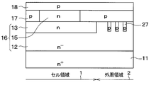
- FIGS. 1 to 3 The first embodiment will be described with reference to FIGS. 1 to 3.
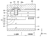
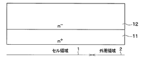
- Cell region 1 in FIG. 2 corresponds to a cross-sectional view taken along line II-II in FIG. 1
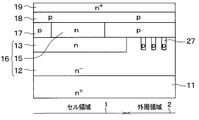
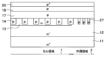
- cell region 1 in FIG. 3 is a cross-sectional view taken along line III-III in FIG. It corresponds to FIG. 1 is a perspective sectional view of one cell in the cell region 1 of the MOSFET.
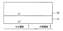
- the SiC semiconductor device includes an n + -type substrate 11 made of SiC.
- the substrate 11 has an off angle of 0 to 8 ° with respect to the (0001) Si plane, and the concentration of n-type impurities such as nitrogen and phosphorus is, for example, 1.0 ⁇ 10 19 / cm 3. And the thickness of about 300 ⁇ m is used.
- the surface direction of the substrate 11 is the xy plane
- the ⁇ 11-20> direction in the xy plane is the y axis direction
- the direction orthogonal to the y axis direction is the x axis direction
- the normal direction to the surface direction of the substrate 11 is the z-axis direction.
- n ⁇ made of SiC having an n-type impurity concentration of, for example, 5.0 to 10.0 ⁇ 10 15 / cm 3 and a thickness of approximately 10 to 15 ⁇ m, such as nitrogen and phosphorus.
- a mold layer 12 is formed.
- the impurity concentration of the n -- type layer 12 may be constant in the depth direction, but the concentration distribution is inclined and the side of the n -- type layer 12 closer to the substrate 11 is closer to the side away from the substrate 11 It is preferable that the concentration be high.
- the impurity concentration in a portion about 3 to 5 ⁇ m from the surface of the substrate 11 may be higher than the other portion by about 2.0 ⁇ 10 15 / cm 3 . With such a configuration, the internal resistance of the n -- type layer 12 can be reduced, and the on-resistance can be reduced.
- the n -- type layer 12 corresponds to the first impurity region.
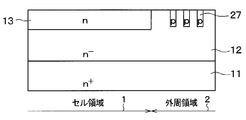
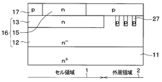
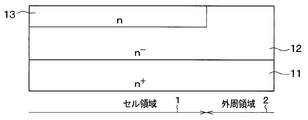
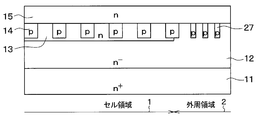
- the first current dispersion layer 13 is made of an n-type impurity such as nitrogen or phosphorus and has a depth of 0.3 to 1.5 ⁇ m. The specific impurity concentration of the first current dispersion layer 13 will be described later.
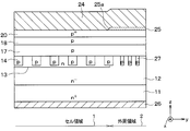
- the first current dispersion layer 13 is formed only in the cell region 1 in the present embodiment. That is, in this embodiment, n - regions where the first current spreading layer 13 is formed is a cell area 1 in a surface portion of the mold layer 12, n - first current spreading layer 13 in a surface portion of the mold layer 12 An area in which no is formed is taken as the outer peripheral area 2.
- a plurality of p-type first deep layers 14 each having a p-type impurity concentration of, for example, 2.0 ⁇ 10 17 to 2.0 ⁇ 10 18 are formed in the first current dispersion layer 13.
- the plurality of first deep layers 14 are respectively extended along the x-axis direction so as to be in the form of stripes, and are arranged at equal intervals along the y-axis direction.
- the first deep layer 14 is formed shallower than the first current dispersion layer 13. That is, the first deep layer 14 is formed so that the bottom portion thereof is located in the first current distribution layer 13. In other words, the first deep layer 14 is formed such that the first current distribution layer 13 is located between the first deep layer 14 and the n ⁇ -type layer 12.
- the first deep layer 14 is formed by ion implantation as described later, but in consideration of the processing limit of photolithography at the time of ion implantation, the length in the y-axis direction is 0.3 ⁇ m or more It is formed to be In addition, an interval along the y-axis direction of the adjacent first deep layers 14, that is, a width along the y-axis direction of the first current distribution layer 13 sandwiched by the adjacent first deep layers 14 (hereinafter simply referred to as the first width The width of the current dispersion layer 13 will be described later. However, the distance between adjacent first deep layers 14 is smaller than the distance between adjacent trenches 21 described later.
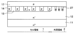
- the concentration of an n-type impurity such as nitrogen or phosphorus is, for example, 1.0 ⁇ 10 16 to 5.0 ⁇ 10 17 and the thickness is 0.5 to A second current dispersion layer 15 of 2 ⁇ m is formed.
- the drift layer 16 is configured to include the n ⁇ -type layer 12, the first current distribution layer 13, and the second current distribution layer 15.
- the second current spreading layer 15, the so as to penetrate the second current spreading layer 15 is a p-type impurity concentration of, for example, 2.0 ⁇ 10 17 ⁇ 2.0 ⁇ 10 18 , such as boron, thickness
- a plurality of second deep layers 17 equal to the second current distribution layer 15 are formed.
- the second deep layer 17 is extended along the y-axis direction. That is, the second deep layers 17 are extended in the direction intersecting the respective first deep layers 14.
- each 2nd deep layer 17 is connected with a plurality of 1st deep layers 14, respectively. Further, the plurality of second deep layers 17 are formed apart from the trench 21 while sandwiching the trench 21 described later.
- a P-type base region 18 is formed on the second current distribution layer 15 and the second deep layer 17.
- an n + -type source region 19 and a p + -type contact layer 20 are formed in the surface layer portion of the base region 18.
- the source region 19 is disposed on both sides of a trench gate structure described later, and the contact layer 20 is provided on the opposite side to the trench gate structure with the source region 19 interposed therebetween. Further, in the present embodiment, the source region 19 corresponds to a second impurity region.
- the base region 18 is configured to have a p-type impurity concentration of, for example, boron or the like of about 5.0 ⁇ 10 16 to 2.0 ⁇ 10 19 / cm 3 and a thickness of about 2.0 ⁇ m.
- the source region 19 is configured such that the concentration of an n-type impurity such as nitrogen or phosphorus (i.e., the surface concentration) in the surface layer portion is, for example, 1.0 ⁇ 10 21 / cm 3 and the thickness is about 0.3 ⁇ m.
- the contact layer 20 has, for example, a p-type impurity concentration (i.e., surface concentration) of boron or the like in the surface layer portion, for example, about 1.0 ⁇ 10 21 / cm 3 and a thickness of about 0.3 ⁇ m.
- the width is, for example, 1.4 to 2.0 ⁇ m so that the bottom surface is located in the second current distribution layer 15 while reaching the second current distribution layer 15 through the base region 18 and the source region 19.
- Trenches 21 are formed. That is, the trench 21 is formed so as not to reach the first current distribution layer 13 and the first deep layer 14. That is, the trench 21 is formed such that the first current distribution layer 13 and the first deep layer 14 are located below the bottom surface of the trench 21. Since trench 21 is formed to penetrate base region 18 and source region 19, it can be said that base region 18 and source region 19 are formed in contact with the side surface of trench 21.
- the trench 21 is filled with a gate insulating film 22 formed on the inner wall surface and a gate electrode 23 formed of doped polysilicon formed on the surface of the gate insulating film 22.
- a trench gate structure is configured.
- the gate insulating film 22 is formed by thermally oxidizing the inner wall surface of the trench 21 and has a thickness of about 100 nm on both the side and bottom sides of the trench 21.
- the trench gate structure is configured as described above.
- the trench 21 is extended with the y-axis direction (that is, the ⁇ -1120> direction) in FIG. 1 as the longitudinal direction.
- the trench 21 is extended in the ⁇ 11-20> direction in this manner, whereby formation of a facet on the (1-100) plane which is the sidewall surface of the trench 21 can be suppressed.
- the (1-100) plane can be used as a channel, the influence of channel mobility dependence can be reduced.
- the trenches 21 are actually formed in a stripe shape by being formed by arranging a plurality of the trenches 21 along the x-axis direction in FIG. Further, the source region 19 and the contact layer 20 described above are extended along the extending direction of the trench 21.
- a source electrode 24 and a gate wiring are formed on the surface of the source region 19 and the contact layer 20 and the surface of the gate electrode 23.
- the source electrode 24 corresponds to the first electrode.
- the source electrode 24 and the gate wiring are made of a plurality of metals (for example, Ni / Al etc.), and at least a portion in contact with n-type SiC (ie, the source region 19 and the gate electrode 23 in the case of n doping) It is composed of n-type SiC and a metal capable of ohmic contact. Further, at least portions of the source electrode 24 and the gate wiring in contact with p-type SiC (that is, the contact layer 20 and the gate electrode 23 in the case of p doping) are made of metal that can make ohmic contact with p-type SiC.
- metals for example, Ni / Al etc.
- the source electrode 24 and the gate wiring are electrically insulated by being formed on the interlayer insulating film 25.
- the source electrode 24 is electrically connected to the source region 19 and the contact layer 20 through the contact hole 25 a formed in the interlayer insulating film 25.
- the first deep layer 14 is maintained at the same potential as the source electrode 24 through the contact layer 20, the base region 18, and the second deep layer 17.
- the gate wiring is electrically connected to the gate electrode 23 through a contact hole 25a formed in the interlayer insulating film 25 in a cross section different from those in FIGS.
- a drain electrode 26 electrically connected to the substrate 11 is formed on the back surface side of the substrate 11.
- the substrate 11 functions as a drain layer. Further, in the present embodiment, the drain electrode 26 corresponds to a second electrode.
- an n-channel type MOSFET of an inverted trench gate structure is formed.
- a second deep layer 17 formed in the cell region 1 is extended on the n ⁇ -type layer 12.
- a plurality of P-type guard rings 27 connected to the second deep layer 17 and surrounding the cell region 1 are formed.
- the guard ring 27 has the same impurity concentration as the first current distribution layer 13 and the same depth. Note that, as described above, the first current dispersion layer 13 is not formed in the outer peripheral region 2.
- the above is the configuration of the SiC semiconductor device in the present embodiment. Next, the operation of the SiC semiconductor device will be described.
- the inversion layer is not formed in the base region 18 in the OFF state before the gate voltage is applied to the gate electrode 23. Therefore, even if a positive voltage (for example, 1600 V) is applied to the drain electrode 26, no electrons flow from the source region 19 into the base region 18, and a current flows between the source electrode 24 and the drain electrode 26. Not flowing.
- a positive voltage for example, 1600 V
- the first deep layer 14 and the first current distribution layer 13 are provided at a deeper position than the trench 21. Therefore, in this SiC semiconductor device, the depletion layer formed between the first deep layer 14 and the first current distribution layer 13 makes it difficult for the high electric field under the influence of the drain voltage to enter the gate insulating film 22. Therefore, in the present embodiment, destruction of the gate insulating film 22 can be suppressed.
- a predetermined gate voltage for example, 20 V
- a channel is formed on the surface of the base region 18 in contact with the trench 21. Therefore, electrons injected from the source electrode 24 flow from the source region 19 to the second current distribution layer 15 after passing through the channel formed in the base region 18.
- the electrons having flowed to the second current distribution layer 15 pass through the first current distribution layer 13 to flow to the n ⁇ -type layer 12 and thereafter flow to the drain electrode 26 through the substrate 11 as a drain layer. Thereby, current flows between the source electrode 24 and the drain electrode 26, and the SiC semiconductor device is turned on.
- the second current distribution layer 15 since the electrons having passed through the channel flow through the second current distribution layer 15, the first current distribution layer 13, and the n -- type layer 12 to the substrate 11, the second current distribution layer 15 is formed. It can be said that the drift layer 16 is configured to have the first current distribution layer 13 and the n ⁇ -type layer 12.
- the first current distribution layer 13 and the second current distribution layer 15 have a higher impurity concentration than the n ⁇ -type layer 12. Therefore, the spread of the depletion layer extending from the first deep layer 14 is suppressed as compared with the conventional SiC semiconductor device in which the deep layer is formed in contact with the drift layer. For this reason, narrowing of the current path is suppressed, and the on resistance can be reduced.
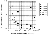
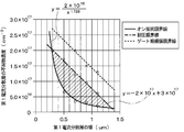
- the on-resistance of the first current distribution layer 13 decreases as the impurity concentration of the first current distribution layer 13 increases. Specifically, the on-resistance of the first current dispersion layer 13 sharply decreases as the impurity concentration increases in the range of 0.5 m ⁇ ⁇ cm 2 or more, and the impurity concentration in the range less than 0.5 m ⁇ ⁇ cm 2. The higher you go, the lower you go.
- the on-resistance also depends on the width of the first current distribution layer 13 and decreases as the width of the first current distribution layer 13 increases. For this reason, in the present embodiment, the impurity concentration and the width of the first current dispersion layer 13 are set such that the on-resistance is less than 0.5 m ⁇ ⁇ cm 2 .
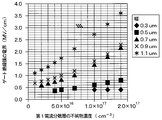
- the electric field applied to the gate insulating film 22 at the off time becomes larger as the impurity concentration of the first current distribution layer 13 becomes higher, and the width of the first current distribution layer 13 becomes wider. growing.
- the impurity concentration and the width of the first current dispersion layer 13 are set such that the electric field applied to the gate insulating film 22 is less than 3.0 MV / cm.
- the withstand voltage decreases as the impurity concentration of the first current distribution layer 13 increases, and decreases as the width of the first current distribution layer 13 increases.
- the withstand voltage of 2000 V is theoretically maximized, and having a withstand voltage of 1600 V is considered to be a sufficiently high withstand voltage. ing.
- the impurity concentration and the width of the first current distribution layer 13 are set so that the breakdown voltage is 1600 V or more.
- FIGS. 4 to 6 are summarized as shown in FIG. Specifically, in FIG. 7, the hatched portions satisfy all of the ON resistance of the first current dispersion layer 13 of FIG. 4, the electric field applied to the gate insulating film 22 of FIG. 5, and the withstand voltage of FIG. It becomes an area.
- the impurity concentration of the first current dispersion layer 13 is y [cm -3 ] and the width of the first current distribution layer 13 is x [ ⁇ m], 2 ⁇ 10 16 / x1 . It is said that 728 ⁇ y ⁇ 2 ⁇ 10 17 x + 3 ⁇ 10 17 .
- the electric field applied to the gate insulating film 22 can be reduced while reducing the on-resistance, and the breakdown voltage can also be suppressed.
- the width of the first current distribution layer 13 is the narrowest portion of the first current distribution layer 13. It corresponds to the length.
- FIGS. 8A to 8J are sectional views corresponding to FIG. 2
- FIGS. 9A to 9H are sectional views corresponding to FIG.
- the n + -type substrate 11 is prepared. Then, an n ⁇ -type layer 12 made of SiC is epitaxially grown on the surface of the substrate 11.
- the substrate 11 used has an area capable of forming the cell area 1 and the outer peripheral area 2.
- a mask (not shown) is formed on the surface of the n ⁇ -type layer 12, and the mask is formed by photolithography or the like so that the formation planned region of the first current dispersion layer 13 is opened. Pattern it. Specifically, the mask is patterned so that only the cell region 1 is opened. Then, an n-type impurity such as nitrogen or phosphorus is ion-implanted from above the mask and heat treatment is performed to form the first current dispersion layer 13 only in the cell region 1. After that, the mask is removed.
- an LTO that is, Low Temperature Oxide
- a mask is used also in the process described later, but for example, an LTO film or the like is used as each mask.
- the first current dispersion layer 13 is thus formed by ion implantation. Therefore, compared to the case where the first current dispersion layer 13 is formed of an epitaxial film, control of the impurity concentration of the first current dispersion layer 13 is facilitated, and variation in characteristics can be suppressed.
- a mask (not shown) is formed, and the mask is patterned by photolithography or the like so that the formation planned regions of the first deep layer 14 and the guard ring 27 are opened. Then, a p-type impurity such as boron is ion-implanted from above the mask and heat treatment is performed to form the first deep layer 14 and the guard ring 27. That is, in the present embodiment, the first deep layer 14 and the guard ring 27 are formed in the same process.
- the first deep layer 14 is in the form of stripes and is formed shallower than the first current dispersion layer 13. Further, as described above, the first current dispersion layer 13 and the first deep layer 14 are formed to satisfy 2 ⁇ 10 16 / x 1.728 ⁇ y ⁇ 2 ⁇ 10 17 x + 3 ⁇ 10 17 .
- the second current distribution layer 15 made of SiC is epitaxially grown on the n ⁇ -type layer 12.
- the drift layer 16 having the n -- type layer 12, the first current distribution layer 13, and the second current distribution layer 15 is formed.
- a mask (not shown) is formed, and the mask is patterned by photolithography or the like so as to open an area for forming the second deep layer 17. Then, a second deep layer 17 is formed by ion implantation of p-type impurities such as boron from above the mask and heat treatment.
- the second deep layer 17 is extended in the direction intersecting with the extending direction of the first deep layer 14. For this reason, even when there is a slight positional deviation when forming the second deep layer 17, it is possible to suppress the occurrence of the problem that the first deep layer 14 and the second deep layer 17 are not connected.
- a base region 18 is formed on the second current distribution layer 15 and the second deep layer 17 by epitaxial growth of a p-type impurity layer.
- a source region 19 is formed on the base region 18 by epitaxial growth of an n-type impurity layer.
- a mask (not shown) is formed, and the mask is patterned by photolithography or the like so that the formation planned region of the contact layer 20 is opened. Then, p-type impurities such as boron are ion-implanted from above the mask and heat treatment is performed to form the contact layer 20.
- the mask is patterned so that the formation travel region of the trench 21 is opened.
- anisotropic etching is performed to form a trench 21.
- the trench 21 is formed to penetrate the source region 19 and the base region 18 and to locate the bottom in the second current distribution layer 15. That is, the trench 21 is formed so that the first current distribution layer 13 and the first deep layer 14 are located below the bottom surface of the trench 21.
- the gate insulating film 22 is formed at a location including the inside of the trench 21.
- the gate insulating film 22 is formed by gate oxidation (that is, thermal oxidation) by a pyrogenic method using a wet atmosphere.
- a polysilicon layer doped with n-type impurities is formed on the surface of the gate insulating film 22 to a thickness of about 440 nm at a temperature of 600 ° C., for example, so that the gate insulating film 22 and the gate electrode 23 remain in the trench 21.
- An etch back process etc. are performed. This forms a trench gate structure.
- the interlayer insulating film 25 is formed. Then, the contact hole 25a where part of the source region 19 and the contact layer 20 are exposed, and the contact hole where part of the gate electrode 23 is exposed are formed. Next, an electrode material is deposited to fill each contact hole 25a, and then the electrode material is patterned to form a source electrode 24 and a gate wiring. Further, the drain electrode 26 is formed on the back surface side of the substrate 11. As described above, the SiC semiconductor device of the present embodiment is manufactured.
- the first current distribution layer 13 having a higher impurity concentration than the n ⁇ -type layer 12 and the first current distribution layer 13 are formed at a deeper position than the trench 21. And the formed first deep layer 14. Therefore, it becomes difficult for a high electric field to enter the gate insulating film 22, and the destruction of the gate insulating film 22 can be suppressed.
- the first current distribution layer 13 has a higher impurity concentration than the n -- type layer 12, the first deep is compared with the conventional SiC semiconductor device in which the deep layer is formed in contact with the drift layer.
- the spread of the depletion layer extending from the layer 14 is suppressed. Therefore, the narrowing of the current path by the first deep layer 14 is suppressed, and the on resistance can be reduced.
- the first current distribution layer 13 and the first deep layer 14 are formed at a deeper position than the trench 21. For this reason, even when misalignment or the like occurs when forming the first deep layer 14, it is possible to suppress contact between the first deep layer 14 and the trench 21.
- the first deep layer 14 is formed in the first current distribution layer 13. That is, the first deep layer 14 is formed such that the first current distribution layer 13 is located between the bottom of the first deep layer 14 and the n ⁇ -type layer 12. Therefore, the depletion layer extending from the first deep layer 14 largely extends to the n -- type layer 12 side, and it is possible to suppress an increase in the on-resistance.
- the second deep layer 17 is extended in the direction intersecting with the extending direction of the first deep layer 14. For this reason, compared with the case where the second deep layer 17 is extended along the extending direction of the first deep layer 14, the second deep layer 17 and the first deep layer 14 and the second deep layer 17 are not It is possible to suppress the occurrence of the problem that no connection occurs. That is, it is possible to suppress the occurrence of the problem that the first deep layer 14 is in the floating state.
- the second deep layer 17 mainly exerts the function of connecting the first deep layer 14 and the base region 18 (that is, the source electrode 24), and is formed at a position away from the trench 21. Therefore, as compared with the case where the second deep layer 17 is in contact with the trench 21, when the electrons having passed through the channel formed in the base region 18 flow to the second current dispersion layer 15, the second current dispersion layer 15 is It can suppress that the path which flows into becomes narrow. Therefore, the increase in on-resistance can be suppressed.
- the second current distribution layer 15 has a higher impurity concentration than the n ⁇ -type layer 12. Therefore, for example, as compared with the case where the second current distribution layer 15 has the same impurity concentration as the n -- type layer 12, the spread of the depletion layer extending from the second deep layer 17 is also suppressed. That is, narrowing of the current path in the first current distribution layer 13 can be suppressed. Therefore, the increase in on-resistance can be suppressed.
- the impurity concentration of the first current dispersion layer 13 is y [cm ⁇ 3 ] and the width of the first current distribution layer 13 is x [ ⁇ m], 2 It is formed so that x 10 16 / x 1. 728 ⁇ y ⁇ -2 x 10 17 x + 3 x 10 17 . Therefore, it is possible to reduce the electric field applied to the gate insulating film 22 while reducing the on-resistance, and to suppress the reduction in the withstand voltage.
- the first current distribution layer 13 is formed only in the cell region 1 and not formed in the outer peripheral region 2. Therefore, in the outer peripheral region 2, the depletion layer is easily spread, and the interval of the equipotential lines is easily spread, so that the electric field concentration can be hardly generated. Therefore, the freedom of design can be improved.
- the first current distribution layer 13 is formed by ion implantation. Therefore, compared to the case where the first current dispersion layer 13 is formed of an epitaxial film, control of the impurity concentration of the first current dispersion layer 13 is facilitated, and variation in characteristics can be suppressed.
- Second Embodiment The second embodiment will be described.
- the configuration of the first deep layer 14 is changed, and the other parts are the same as in the first embodiment, and thus the description thereof is omitted here.
- a plurality of first deep layers 14 are extended along the x-axis direction. Then, the adjacent first deep layers 14 are connected at a plurality of places. That is, in the present embodiment, it can be said that the first deep layer 14 is formed in a lattice shape.
- the length of the narrowest portion of the first current distribution layer 13 is the width x. That is, for example, in FIG. 10, the first current dispersion layer 13 has a square planar shape in a portion surrounded by the first deep layer 14, but when the planar shape is a rectangular shape, the length of the short side is Is the width x.
- the first deep layers 14 are formed in a lattice shape. Therefore, it is possible to obtain the same effect as that of the first embodiment while further suppressing the occurrence of the problem that the first deep layer 14 and the second deep layer 17 are not connected.
- an n-channel MOSFET in which the first conductivity type is n-type and the second conductivity type is p-type is described as an example, but p is the conductivity type of each component inverted. It may be a channel type MOSFET.
- the MOSFET having the trench gate structure has been described as an example, but an IGBT having a similar trench gate structure may be used. The IGBT only changes the conductivity type of the substrate 11 from n-type to p-type in each of the above embodiments, and the other structure and manufacturing method are the same as in the above embodiments.
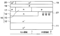
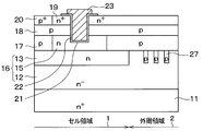
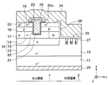
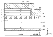
- the outer peripheral region 2 may have a mesa structure. That is, as shown in FIG. 11 and FIG. 12, the outer peripheral region 2 may have a mesa structure in which a recess 28 which penetrates the source region 19 and the base region 18 and reaches the n ⁇ -type layer 12 is formed.
- Cell region 1 in FIG. 11 corresponds to a cross section taken along line II-II in FIG. 1
- cell region 1 in FIG. 12 corresponds to a cross section taken along line III-III in FIG. .
- the second deep layer 17 may not be formed in plural but may be only one. Even in such a SiC semiconductor device, when one second deep layer 17 is connected to each first deep layer 14, it is possible to obtain the same effect as that of each embodiment described above.
- the first deep layer 14 may extend, for example, along the y-axis direction. That is, the first deep layer 14 may be extended in the same direction as the second deep layer 17.
- the second current dispersion layer 15 may have, for example, the same impurity concentration as the n ⁇ -type layer 12.
- the first current distribution layer 13 may be formed also in the outer peripheral region 2.
- the first current dispersion layer 13 and the first deep layer 14 may not be formed to satisfy 2 ⁇ 10 16 / x 1.728 ⁇ y ⁇ 2 ⁇ 10 17 x + 3 ⁇ 10 17 .
- the contact layer 20 may not be formed. That is, the source electrode 24 may be connected to the base region 18.
- the gate insulating film 22 may be configured to include an oxide film, a nitride film, or the like that is not generated by thermal oxidation.
- the source region 19 may be formed after the contact layer 20 is formed by epitaxially growing a p-type impurity layer on the base region 18.
- a bar (-) should normally be added above the desired number, but since there is a limitation in expression based on the electronic application, it is desirable in the present specification to be a desired one. A bar shall be put in front of the numbers.
Landscapes
- Electrodes Of Semiconductors (AREA)
Priority Applications (2)
| Application Number | Priority Date | Filing Date | Title |
|---|---|---|---|
| CN201880055698.3A CN111066152B (zh) | 2017-08-31 | 2018-08-29 | 碳化硅半导体装置及其制造方法 |
| US16/776,821 US11063145B2 (en) | 2017-08-31 | 2020-01-30 | Silicon carbide semiconductor device and method for manufacturing same |
Applications Claiming Priority (2)
| Application Number | Priority Date | Filing Date | Title |
|---|---|---|---|
| JP2017166882A JP6729523B2 (ja) | 2017-08-31 | 2017-08-31 | 炭化珪素半導体装置およびその製造方法 |
| JP2017-166882 | 2017-08-31 |
Related Child Applications (2)
| Application Number | Title | Priority Date | Filing Date |
|---|---|---|---|
| US16/776,821 Continuation US11063145B2 (en) | 2017-08-31 | 2020-01-30 | Silicon carbide semiconductor device and method for manufacturing same |
| US16/776,821 Continuation-In-Part US11063145B2 (en) | 2017-08-31 | 2020-01-30 | Silicon carbide semiconductor device and method for manufacturing same |
Publications (1)
| Publication Number | Publication Date |
|---|---|
| WO2019044921A1 true WO2019044921A1 (ja) | 2019-03-07 |
Family
ID=65525716
Family Applications (1)
| Application Number | Title | Priority Date | Filing Date |
|---|---|---|---|
| PCT/JP2018/032004 Ceased WO2019044921A1 (ja) | 2017-08-31 | 2018-08-29 | 炭化珪素半導体装置およびその製造方法 |
Country Status (4)
| Country | Link |
|---|---|
| US (1) | US11063145B2 (enExample) |
| JP (1) | JP6729523B2 (enExample) |
| CN (1) | CN111066152B (enExample) |
| WO (1) | WO2019044921A1 (enExample) |
Cited By (5)
| Publication number | Priority date | Publication date | Assignee | Title |
|---|---|---|---|---|
| US20210184031A1 (en) * | 2019-12-12 | 2021-06-17 | Denso Corporation | Silicon carbide semiconductor device |
| WO2022202936A1 (ja) * | 2021-03-24 | 2022-09-29 | 株式会社デンソー | 炭化珪素半導体装置およびそれを用いたインバータ回路、炭化珪素半導体装置の製造方法 |
| JP2022151776A (ja) * | 2021-03-24 | 2022-10-07 | 株式会社デンソー | 炭化珪素半導体装置およびそれを用いたインバータ回路、炭化珪素半導体装置の製造方法 |
| JP2023048630A (ja) * | 2021-09-28 | 2023-04-07 | 株式会社デンソー | 半導体装置およびその製造方法 |
| US20230143618A1 (en) * | 2021-11-09 | 2023-05-11 | Denso Corporation | Semiconductor device and method for manufacturing the same |
Families Citing this family (20)
| Publication number | Priority date | Publication date | Assignee | Title |
|---|---|---|---|---|
| JP7180402B2 (ja) | 2019-01-21 | 2022-11-30 | 株式会社デンソー | 半導体装置 |
| JP7379880B2 (ja) * | 2019-06-21 | 2023-11-15 | 富士電機株式会社 | 半導体装置 |
| JP7443924B2 (ja) | 2020-05-14 | 2024-03-06 | 富士電機株式会社 | 半導体装置 |
| JP7532921B2 (ja) | 2020-06-09 | 2024-08-14 | 富士電機株式会社 | 半導体装置 |
| JP7458257B2 (ja) | 2020-07-09 | 2024-03-29 | 株式会社東芝 | 半導体装置、インバータ回路、駆動装置、車両、及び、昇降機 |
| JP2022021181A (ja) | 2020-07-21 | 2022-02-02 | 株式会社デンソー | 半導体装置 |
| KR102812224B1 (ko) * | 2021-03-03 | 2025-05-22 | 주식회사 디비하이텍 | 에피택셜층의 유효 두께 차등 구조를 가지는 슈퍼정션 반도체 소자 및 제조방법 |
| JP7476132B2 (ja) * | 2021-03-23 | 2024-04-30 | 株式会社東芝 | 半導体装置、インバータ回路、駆動装置、車両、及び、昇降機 |
| JP7593225B2 (ja) * | 2021-05-14 | 2024-12-03 | 株式会社デンソー | 炭化珪素半導体装置 |
| JP7582061B2 (ja) * | 2021-05-14 | 2024-11-13 | 株式会社デンソー | 半導体装置 |
| JP7593235B2 (ja) * | 2021-05-28 | 2024-12-03 | 株式会社デンソー | 半導体装置 |
| JP7619168B2 (ja) * | 2021-06-01 | 2025-01-22 | 株式会社デンソー | 半導体装置 |
| JP7673513B2 (ja) * | 2021-06-15 | 2025-05-09 | 株式会社デンソー | 半導体装置 |
| JP7651403B2 (ja) | 2021-08-05 | 2025-03-26 | 株式会社デンソー | 電界効果トランジスタとその製造方法 |
| JP7683466B2 (ja) * | 2021-11-17 | 2025-05-27 | 株式会社デンソー | 半導体装置およびその製造方法 |
| JP7717010B2 (ja) * | 2022-03-08 | 2025-08-01 | 株式会社デンソー | 半導体装置 |
| JP7757235B2 (ja) * | 2022-05-13 | 2025-10-21 | 株式会社デンソー | 半導体装置とその製造方法 |
| JP2024025440A (ja) * | 2022-08-12 | 2024-02-26 | 株式会社デンソー | 炭化珪素半導体装置 |
| CN119968936A (zh) * | 2023-09-04 | 2025-05-09 | 株式会社东芝 | 半导体装置 |
| CN118800806B (zh) * | 2024-09-11 | 2025-01-10 | 陕西半导体先导技术中心有限公司 | 一种带有突出p阱的umosfet器件及其制备方法 |
Citations (4)
| Publication number | Priority date | Publication date | Assignee | Title |
|---|---|---|---|---|
| JP2008227356A (ja) * | 2007-03-15 | 2008-09-25 | Toyota Central R&D Labs Inc | 半導体装置とその製造方法 |
| US20140021484A1 (en) * | 2012-07-19 | 2014-01-23 | Infineon Technologies Ag | Semiconductor Device |
| WO2014199465A1 (ja) * | 2013-06-12 | 2014-12-18 | 三菱電機株式会社 | 半導体装置 |
| JP2015192027A (ja) * | 2014-03-28 | 2015-11-02 | 国立研究開発法人産業技術総合研究所 | 炭化珪素半導体装置およびその製造方法 |
Family Cites Families (9)
| Publication number | Priority date | Publication date | Assignee | Title |
|---|---|---|---|---|
| CN100565879C (zh) * | 2008-01-08 | 2009-12-02 | 苏州硅能半导体科技股份有限公司 | 一种深沟槽大功率mos器件及其制造方法 |
| EP2091083A3 (en) | 2008-02-13 | 2009-10-14 | Denso Corporation | Silicon carbide semiconductor device including a deep layer |
| JP2009302436A (ja) * | 2008-06-17 | 2009-12-24 | Denso Corp | 炭化珪素半導体装置の製造方法 |
| US8415671B2 (en) * | 2010-04-16 | 2013-04-09 | Cree, Inc. | Wide band-gap MOSFETs having a heterojunction under gate trenches thereof and related methods of forming such devices |
| JP5531787B2 (ja) * | 2010-05-31 | 2014-06-25 | 株式会社デンソー | 炭化珪素半導体装置およびその製造方法 |
| JP5728992B2 (ja) | 2011-02-11 | 2015-06-03 | 株式会社デンソー | 炭化珪素半導体装置およびその製造方法 |
| JP2012169384A (ja) * | 2011-02-11 | 2012-09-06 | Denso Corp | 炭化珪素半導体装置およびその製造方法 |
| JP5812029B2 (ja) * | 2012-06-13 | 2015-11-11 | 株式会社デンソー | 炭化珪素半導体装置およびその製造方法 |
| JP2015072999A (ja) * | 2013-10-02 | 2015-04-16 | 株式会社デンソー | 炭化珪素半導体装置 |
-
2017
- 2017-08-31 JP JP2017166882A patent/JP6729523B2/ja active Active
-
2018
- 2018-08-29 WO PCT/JP2018/032004 patent/WO2019044921A1/ja not_active Ceased
- 2018-08-29 CN CN201880055698.3A patent/CN111066152B/zh active Active
-
2020
- 2020-01-30 US US16/776,821 patent/US11063145B2/en active Active
Patent Citations (4)
| Publication number | Priority date | Publication date | Assignee | Title |
|---|---|---|---|---|
| JP2008227356A (ja) * | 2007-03-15 | 2008-09-25 | Toyota Central R&D Labs Inc | 半導体装置とその製造方法 |
| US20140021484A1 (en) * | 2012-07-19 | 2014-01-23 | Infineon Technologies Ag | Semiconductor Device |
| WO2014199465A1 (ja) * | 2013-06-12 | 2014-12-18 | 三菱電機株式会社 | 半導体装置 |
| JP2015192027A (ja) * | 2014-03-28 | 2015-11-02 | 国立研究開発法人産業技術総合研究所 | 炭化珪素半導体装置およびその製造方法 |
Cited By (9)
| Publication number | Priority date | Publication date | Assignee | Title |
|---|---|---|---|---|
| US20210184031A1 (en) * | 2019-12-12 | 2021-06-17 | Denso Corporation | Silicon carbide semiconductor device |
| US11538935B2 (en) * | 2019-12-12 | 2022-12-27 | Denso Corporation | Silicon carbide semiconductor device |
| WO2022202936A1 (ja) * | 2021-03-24 | 2022-09-29 | 株式会社デンソー | 炭化珪素半導体装置およびそれを用いたインバータ回路、炭化珪素半導体装置の製造方法 |
| JP2022151776A (ja) * | 2021-03-24 | 2022-10-07 | 株式会社デンソー | 炭化珪素半導体装置およびそれを用いたインバータ回路、炭化珪素半導体装置の製造方法 |
| JP7521553B2 (ja) | 2021-03-24 | 2024-07-24 | 株式会社デンソー | 炭化珪素半導体装置およびそれを用いたインバータ回路、炭化珪素半導体装置の製造方法 |
| JP2023048630A (ja) * | 2021-09-28 | 2023-04-07 | 株式会社デンソー | 半導体装置およびその製造方法 |
| JP7687171B2 (ja) | 2021-09-28 | 2025-06-03 | 株式会社デンソー | 半導体装置およびその製造方法 |
| US20230143618A1 (en) * | 2021-11-09 | 2023-05-11 | Denso Corporation | Semiconductor device and method for manufacturing the same |
| US12426319B2 (en) * | 2021-11-09 | 2025-09-23 | Denso Corporation | Semiconductor device and method for manufacturing the same |
Also Published As
| Publication number | Publication date |
|---|---|
| CN111066152B (zh) | 2023-07-21 |
| JP6729523B2 (ja) | 2020-07-22 |
| US20200168732A1 (en) | 2020-05-28 |
| US11063145B2 (en) | 2021-07-13 |
| JP2019046908A (ja) | 2019-03-22 |
| CN111066152A (zh) | 2020-04-24 |
Similar Documents
| Publication | Publication Date | Title |
|---|---|---|
| US11063145B2 (en) | Silicon carbide semiconductor device and method for manufacturing same | |
| US11769801B2 (en) | Silicon carbide semiconductor device with cell section and outer periphery section | |
| JP5939448B2 (ja) | 半導体装置及びその製造方法 | |
| WO2019054459A1 (ja) | 半導体装置およびその製造方法 | |
| CN107615492A (zh) | 半导体装置及其制造方法 | |
| JPWO2017064949A1 (ja) | 半導体装置および半導体装置の製造方法 | |
| JP2012169385A (ja) | 炭化珪素半導体装置 | |
| WO2015049838A1 (ja) | 炭化珪素半導体装置 | |
| US11538935B2 (en) | Silicon carbide semiconductor device | |
| WO2013187017A1 (ja) | 炭化珪素半導体装置およびその製造方法 | |
| JP7593225B2 (ja) | 炭化珪素半導体装置 | |
| US10714611B2 (en) | Silicon carbide semiconductor device | |
| US12464791B2 (en) | Semiconductor device | |
| US20230111246A1 (en) | Semiconductor device and method for manufacturing the same | |
| US12426319B2 (en) | Semiconductor device and method for manufacturing the same | |
| JP7439746B2 (ja) | 炭化珪素半導体装置 | |
| US11967634B2 (en) | Semiconductor device and method of manufacturing the same | |
| JP2018110163A (ja) | 炭化珪素半導体装置および炭化珪素半導体装置の製造方法 | |
| JP7683465B2 (ja) | 炭化珪素半導体装置およびその製造方法 | |
| JP7593235B2 (ja) | 半導体装置 | |
| WO2025258666A1 (ja) | 半導体装置 |
Legal Events
| Date | Code | Title | Description |
|---|---|---|---|
| 121 | Ep: the epo has been informed by wipo that ep was designated in this application |
Ref document number: 18849763 Country of ref document: EP Kind code of ref document: A1 |
|
| NENP | Non-entry into the national phase |
Ref country code: DE |
|
| 122 | Ep: pct application non-entry in european phase |
Ref document number: 18849763 Country of ref document: EP Kind code of ref document: A1 |