WO2019017104A1 - 半導体装置 - Google Patents
半導体装置 Download PDFInfo
- Publication number
- WO2019017104A1 WO2019017104A1 PCT/JP2018/021772 JP2018021772W WO2019017104A1 WO 2019017104 A1 WO2019017104 A1 WO 2019017104A1 JP 2018021772 W JP2018021772 W JP 2018021772W WO 2019017104 A1 WO2019017104 A1 WO 2019017104A1
- Authority
- WO
- WIPO (PCT)
- Prior art keywords
- region
- semiconductor
- fwd
- trench
- igbt
- Prior art date
- Legal status (The legal status is an assumption and is not a legal conclusion. Google has not performed a legal analysis and makes no representation as to the accuracy of the status listed.)
- Ceased
Links
Images



Classifications
-
- H—ELECTRICITY
- H10—SEMICONDUCTOR DEVICES; ELECTRIC SOLID-STATE DEVICES NOT OTHERWISE PROVIDED FOR
- H10D—INORGANIC ELECTRIC SEMICONDUCTOR DEVICES
- H10D84/00—Integrated devices formed in or on semiconductor substrates that comprise only semiconducting layers, e.g. on Si wafers or on GaAs-on-Si wafers
- H10D84/40—Integrated devices formed in or on semiconductor substrates that comprise only semiconducting layers, e.g. on Si wafers or on GaAs-on-Si wafers characterised by the integration of at least one component covered by groups H10D12/00 or H10D30/00 with at least one component covered by groups H10D10/00 or H10D18/00, e.g. integration of IGFETs with BJTs
- H10D84/401—Combinations of FETs or IGBTs with BJTs
- H10D84/403—Combinations of FETs or IGBTs with BJTs and with one or more of diodes, resistors or capacitors
- H10D84/406—Combinations of FETs or IGBTs with vertical BJTs and with one or more of diodes, resistors or capacitors
-
- H—ELECTRICITY
- H10—SEMICONDUCTOR DEVICES; ELECTRIC SOLID-STATE DEVICES NOT OTHERWISE PROVIDED FOR
- H10D—INORGANIC ELECTRIC SEMICONDUCTOR DEVICES
- H10D62/00—Semiconductor bodies, or regions thereof, of devices having potential barriers
- H10D62/10—Shapes, relative sizes or dispositions of the regions of the semiconductor bodies; Shapes of the semiconductor bodies
- H10D62/13—Semiconductor regions connected to electrodes carrying current to be rectified, amplified or switched, e.g. source or drain regions
- H10D62/141—Anode or cathode regions of thyristors; Collector or emitter regions of gated bipolar-mode devices, e.g. of IGBTs
- H10D62/142—Anode regions of thyristors or collector regions of gated bipolar-mode devices
-
- H—ELECTRICITY
- H10—SEMICONDUCTOR DEVICES; ELECTRIC SOLID-STATE DEVICES NOT OTHERWISE PROVIDED FOR
- H10D—INORGANIC ELECTRIC SEMICONDUCTOR DEVICES
- H10D12/00—Bipolar devices controlled by the field effect, e.g. insulated-gate bipolar transistors [IGBT]
-
- H—ELECTRICITY
- H10—SEMICONDUCTOR DEVICES; ELECTRIC SOLID-STATE DEVICES NOT OTHERWISE PROVIDED FOR
- H10D—INORGANIC ELECTRIC SEMICONDUCTOR DEVICES
- H10D12/00—Bipolar devices controlled by the field effect, e.g. insulated-gate bipolar transistors [IGBT]
- H10D12/411—Insulated-gate bipolar transistors [IGBT]
- H10D12/441—Vertical IGBTs
- H10D12/461—Vertical IGBTs having non-planar surfaces, e.g. having trenches, recesses or pillars in the surfaces of the emitter, base or collector regions
- H10D12/481—Vertical IGBTs having non-planar surfaces, e.g. having trenches, recesses or pillars in the surfaces of the emitter, base or collector regions having gate structures on slanted surfaces, on vertical surfaces, or in grooves, e.g. trench gate IGBTs
-
- H—ELECTRICITY
- H10—SEMICONDUCTOR DEVICES; ELECTRIC SOLID-STATE DEVICES NOT OTHERWISE PROVIDED FOR
- H10D—INORGANIC ELECTRIC SEMICONDUCTOR DEVICES
- H10D30/00—Field-effect transistors [FET]
- H10D30/60—Insulated-gate field-effect transistors [IGFET]
-
- H—ELECTRICITY
- H10—SEMICONDUCTOR DEVICES; ELECTRIC SOLID-STATE DEVICES NOT OTHERWISE PROVIDED FOR
- H10D—INORGANIC ELECTRIC SEMICONDUCTOR DEVICES
- H10D62/00—Semiconductor bodies, or regions thereof, of devices having potential barriers
- H10D62/10—Shapes, relative sizes or dispositions of the regions of the semiconductor bodies; Shapes of the semiconductor bodies
-
- H—ELECTRICITY
- H10—SEMICONDUCTOR DEVICES; ELECTRIC SOLID-STATE DEVICES NOT OTHERWISE PROVIDED FOR
- H10D—INORGANIC ELECTRIC SEMICONDUCTOR DEVICES
- H10D62/00—Semiconductor bodies, or regions thereof, of devices having potential barriers
- H10D62/10—Shapes, relative sizes or dispositions of the regions of the semiconductor bodies; Shapes of the semiconductor bodies
- H10D62/102—Constructional design considerations for preventing surface leakage or controlling electric field concentration
- H10D62/103—Constructional design considerations for preventing surface leakage or controlling electric field concentration for increasing or controlling the breakdown voltage of reverse-biased devices
-
- H—ELECTRICITY
- H10—SEMICONDUCTOR DEVICES; ELECTRIC SOLID-STATE DEVICES NOT OTHERWISE PROVIDED FOR
- H10D—INORGANIC ELECTRIC SEMICONDUCTOR DEVICES
- H10D62/00—Semiconductor bodies, or regions thereof, of devices having potential barriers
- H10D62/10—Shapes, relative sizes or dispositions of the regions of the semiconductor bodies; Shapes of the semiconductor bodies
- H10D62/124—Shapes, relative sizes or dispositions of the regions of semiconductor bodies or of junctions between the regions
- H10D62/126—Top-view geometrical layouts of the regions or the junctions
- H10D62/127—Top-view geometrical layouts of the regions or the junctions of cellular field-effect devices, e.g. multicellular DMOS transistors or IGBTs
-
- H—ELECTRICITY
- H10—SEMICONDUCTOR DEVICES; ELECTRIC SOLID-STATE DEVICES NOT OTHERWISE PROVIDED FOR
- H10D—INORGANIC ELECTRIC SEMICONDUCTOR DEVICES
- H10D62/00—Semiconductor bodies, or regions thereof, of devices having potential barriers
- H10D62/10—Shapes, relative sizes or dispositions of the regions of the semiconductor bodies; Shapes of the semiconductor bodies
- H10D62/129—Cathode regions of diodes
-
- H—ELECTRICITY
- H10—SEMICONDUCTOR DEVICES; ELECTRIC SOLID-STATE DEVICES NOT OTHERWISE PROVIDED FOR
- H10D—INORGANIC ELECTRIC SEMICONDUCTOR DEVICES
- H10D62/00—Semiconductor bodies, or regions thereof, of devices having potential barriers
- H10D62/10—Shapes, relative sizes or dispositions of the regions of the semiconductor bodies; Shapes of the semiconductor bodies
- H10D62/13—Semiconductor regions connected to electrodes carrying current to be rectified, amplified or switched, e.g. source or drain regions
- H10D62/141—Anode or cathode regions of thyristors; Collector or emitter regions of gated bipolar-mode devices, e.g. of IGBTs
- H10D62/145—Emitter regions of IGBTs
-
- H—ELECTRICITY
- H10—SEMICONDUCTOR DEVICES; ELECTRIC SOLID-STATE DEVICES NOT OTHERWISE PROVIDED FOR
- H10D—INORGANIC ELECTRIC SEMICONDUCTOR DEVICES
- H10D62/00—Semiconductor bodies, or regions thereof, of devices having potential barriers
- H10D62/10—Shapes, relative sizes or dispositions of the regions of the semiconductor bodies; Shapes of the semiconductor bodies
- H10D62/17—Semiconductor regions connected to electrodes not carrying current to be rectified, amplified or switched, e.g. channel regions
- H10D62/393—Body regions of DMOS transistors or IGBTs
-
- H—ELECTRICITY
- H10—SEMICONDUCTOR DEVICES; ELECTRIC SOLID-STATE DEVICES NOT OTHERWISE PROVIDED FOR
- H10D—INORGANIC ELECTRIC SEMICONDUCTOR DEVICES
- H10D64/00—Electrodes of devices having potential barriers
- H10D64/20—Electrodes characterised by their shapes, relative sizes or dispositions
- H10D64/23—Electrodes carrying the current to be rectified, amplified, oscillated or switched, e.g. sources, drains, anodes or cathodes
-
- H—ELECTRICITY
- H10—SEMICONDUCTOR DEVICES; ELECTRIC SOLID-STATE DEVICES NOT OTHERWISE PROVIDED FOR
- H10D—INORGANIC ELECTRIC SEMICONDUCTOR DEVICES
- H10D64/00—Electrodes of devices having potential barriers
- H10D64/20—Electrodes characterised by their shapes, relative sizes or dispositions
- H10D64/27—Electrodes not carrying the current to be rectified, amplified, oscillated or switched, e.g. gates
- H10D64/311—Gate electrodes for field-effect devices
- H10D64/411—Gate electrodes for field-effect devices for FETs
- H10D64/511—Gate electrodes for field-effect devices for FETs for IGFETs
- H10D64/512—Disposition of the gate electrodes, e.g. buried gates
- H10D64/513—Disposition of the gate electrodes, e.g. buried gates within recesses in the substrate, e.g. trench gates, groove gates or buried gates
-
- H—ELECTRICITY
- H10—SEMICONDUCTOR DEVICES; ELECTRIC SOLID-STATE DEVICES NOT OTHERWISE PROVIDED FOR
- H10D—INORGANIC ELECTRIC SEMICONDUCTOR DEVICES
- H10D8/00—Diodes
- H10D8/411—PN diodes having planar bodies
-
- H—ELECTRICITY
- H10—SEMICONDUCTOR DEVICES; ELECTRIC SOLID-STATE DEVICES NOT OTHERWISE PROVIDED FOR
- H10D—INORGANIC ELECTRIC SEMICONDUCTOR DEVICES
- H10D8/00—Diodes
- H10D8/422—PN diodes having the PN junctions in mesas
-
- H—ELECTRICITY
- H10—SEMICONDUCTOR DEVICES; ELECTRIC SOLID-STATE DEVICES NOT OTHERWISE PROVIDED FOR
- H10D—INORGANIC ELECTRIC SEMICONDUCTOR DEVICES
- H10D84/00—Integrated devices formed in or on semiconductor substrates that comprise only semiconducting layers, e.g. on Si wafers or on GaAs-on-Si wafers
-
- H—ELECTRICITY
- H10—SEMICONDUCTOR DEVICES; ELECTRIC SOLID-STATE DEVICES NOT OTHERWISE PROVIDED FOR
- H10D—INORGANIC ELECTRIC SEMICONDUCTOR DEVICES
- H10D84/00—Integrated devices formed in or on semiconductor substrates that comprise only semiconducting layers, e.g. on Si wafers or on GaAs-on-Si wafers
- H10D84/01—Manufacture or treatment
- H10D84/0123—Integrating together multiple components covered by H10D12/00 or H10D30/00, e.g. integrating multiple IGBTs
- H10D84/0126—Integrating together multiple components covered by H10D12/00 or H10D30/00, e.g. integrating multiple IGBTs the components including insulated gates, e.g. IGFETs
-
- H—ELECTRICITY
- H10—SEMICONDUCTOR DEVICES; ELECTRIC SOLID-STATE DEVICES NOT OTHERWISE PROVIDED FOR
- H10D—INORGANIC ELECTRIC SEMICONDUCTOR DEVICES
- H10D84/00—Integrated devices formed in or on semiconductor substrates that comprise only semiconducting layers, e.g. on Si wafers or on GaAs-on-Si wafers
- H10D84/01—Manufacture or treatment
- H10D84/02—Manufacture or treatment characterised by using material-based technologies
- H10D84/03—Manufacture or treatment characterised by using material-based technologies using Group IV technology, e.g. silicon technology or silicon-carbide [SiC] technology
- H10D84/038—Manufacture or treatment characterised by using material-based technologies using Group IV technology, e.g. silicon technology or silicon-carbide [SiC] technology using silicon technology, e.g. SiGe
-
- H—ELECTRICITY
- H10—SEMICONDUCTOR DEVICES; ELECTRIC SOLID-STATE DEVICES NOT OTHERWISE PROVIDED FOR
- H10D—INORGANIC ELECTRIC SEMICONDUCTOR DEVICES
- H10D84/00—Integrated devices formed in or on semiconductor substrates that comprise only semiconducting layers, e.g. on Si wafers or on GaAs-on-Si wafers
- H10D84/80—Integrated devices formed in or on semiconductor substrates that comprise only semiconducting layers, e.g. on Si wafers or on GaAs-on-Si wafers characterised by the integration of at least one component covered by groups H10D12/00 or H10D30/00, e.g. integration of IGFETs
- H10D84/811—Combinations of field-effect devices and one or more diodes, capacitors or resistors
-
- H—ELECTRICITY
- H10—SEMICONDUCTOR DEVICES; ELECTRIC SOLID-STATE DEVICES NOT OTHERWISE PROVIDED FOR
- H10D—INORGANIC ELECTRIC SEMICONDUCTOR DEVICES
- H10D64/00—Electrodes of devices having potential barriers
- H10D64/111—Field plates
- H10D64/117—Recessed field plates, e.g. trench field plates or buried field plates
-
- H—ELECTRICITY
- H10—SEMICONDUCTOR DEVICES; ELECTRIC SOLID-STATE DEVICES NOT OTHERWISE PROVIDED FOR
- H10D—INORGANIC ELECTRIC SEMICONDUCTOR DEVICES
- H10D89/00—Aspects of integrated devices not covered by groups H10D84/00 - H10D88/00
- H10D89/60—Integrated devices comprising arrangements for electrical or thermal protection, e.g. protection circuits against electrostatic discharge [ESD]
-
- H—ELECTRICITY
- H10—SEMICONDUCTOR DEVICES; ELECTRIC SOLID-STATE DEVICES NOT OTHERWISE PROVIDED FOR
- H10W—GENERIC PACKAGES, INTERCONNECTIONS, CONNECTORS OR OTHER CONSTRUCTIONAL DETAILS OF DEVICES COVERED BY CLASS H10
- H10W40/00—Arrangements for thermal protection or thermal control
Definitions
- the present invention relates to a semiconductor device.
- RC-IGBT Reverse
- IGBT Insulated Gate Bipolar Transistor
- FWD Free Wheeling Diode: free-wheeling diode
- Conducting IGBTs are known.
- FWD region the region where FWD is arranged (hereinafter referred to as FWD region) is arranged in a stripe-like layout as viewed from the front surface of the semiconductor chip.
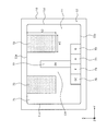
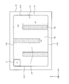
- FIG. 11 and 12 are plan views showing an example of a planar layout of a conventional semiconductor device.
- FIG. 11 shows an example in which the IGBT and the FWD are arranged on the semiconductor chip 110 a (hereinafter, referred to as a small chip IGBT).
- FIG. 12 shows an example in which the FWD is arranged on the same semiconductor chip 110b as the IGBT (hereinafter referred to as a sense IGBT) for detecting and controlling the current and the chip temperature.
- the conventional semiconductor device shown in FIGS. 11 and 12 has an IGBT region 101 and an FWD region 102 in an active region 111.
- the IGBT region 101 is a region in which the IGBT is disposed, and is a region of the active region 111 other than the FWD region 102.
- the total of the surface area of the IGBT region 101 and the surface area of the FWD region 102 is the surface area of the active region 111.
- the FWD regions 102 are arranged in a striped layout, and both ends thereof reach the boundary between the active region 111 and the edge termination region 112. That is, the length (longitudinal length) L102 of the FWD region 102 is substantially the same as the length L101 of one side of the substantially rectangular planar active region 111 parallel to the stripe direction of the FWD region 102. is there.
- the unit cell (constituent unit of the element) of the IGBT in the IGBT region 101 is separately disposed in a plurality of regions.
- electrode pads such as a gate pad (electrode pad) 103 and sense pads 104 to 107 for current and temperature sensing are disposed.
- FIG. 11 shows the case where the gate pad 103 is arranged in the vicinity of one vertex of the active region 111.
- FIG. 12 shows the case where gate pad 103 and sense pads 104 to 106 are arranged along one side of active region 111 orthogonal to the stripe of FWD region 102, and sense pad 107 is arranged near the center.
- Patent Document 1 As a conventional RC-IGBT, a device has been proposed in which four diode regions are arranged in a matrix planar layout, and IGBT regions are arranged so as to surround the four diode regions (for example, Patent Document 1 (see See paragraph 0012, Figures 1, 2, 8 and 10).
- Patent Document 1 the gate trench in the IGBT region and the gate trench in the diode region are arranged in stripes on the same stripe, separated from each other in the extending direction of the stripe, and the end portions thereof are p-type well layers. They are facing each other.
- the conventional RC-IGBT functions as an active region between the plurality of IGBT regions and the plurality of diode regions so as to be orthogonal to the plurality of strip-shaped IGBT regions and the plurality of diode regions.
- An apparatus has been proposed in which non-active areas are arranged (see, for example, Patent Document 2 (paragraph 0067, FIGS. 1 and 2 below)).
- the diode cell regions are disposed apart from each other in the direction in which the diode cell regions extend in a stripe shape, and the end portions thereof face each other via the non-active region.
- the semiconductor chip 110a In order to suppress the temperature rise of the semiconductor chip 110a, it is preferable to increase the number of FWD regions 102 arranged in the active region 111 because the temperature difference between the IGBT region 101 and the FWD region 102 is eliminated.
- the conventional RC-IGBT in the case of the small chip IGBT (see FIG. 11), only one or two FWD regions 102 can be arranged in the active region 111. Therefore, there is a problem that the heat dissipation of the semiconductor chip is deteriorated.
- the width w102 of the FWD region 102 is narrowed and the width w102 of the FWD region 102 is narrowed depending on the area of the FWD region 102 when adjusting the area of the FWD region 102.
- the area needs to be used to increase the number of FWD regions 102.
- the width w102 of the FWD region 102 is too narrow, there is a problem that the forward characteristic of the FWD is deteriorated when a gate voltage of 15 V or more which is a general gate threshold voltage of the IGBT is applied.
- the chip size is large, when adjusting the area of the FWD region 102, it is necessary to narrow the width w102 of the FWD region 102, which causes the same problem as the small chip IGBT.
- the FWD region 102 is in contact with the gate pad 103, so it is necessary to devise a planar layout of the FWD region 102. Further, the width w101 of the IGBT region 101 is narrowed at the portion where the electrode pad is disposed. Also, similarly to the small chip IGBT, the width w102 of the FWD region 102 is also narrow. For this reason, there is a problem that mutual interference occurs at the boundary between the IGBT and the FWD such that the electron current of the IGBT is easily leaked to the FWD region 102, and the element characteristic is deteriorated.
- An object of the present invention is to provide a semiconductor device capable of preventing deterioration of element characteristics or improving the heat dissipation of a semiconductor chip in order to solve the above-mentioned problems caused by the prior art. Furthermore, it is an object of the present invention to provide a semiconductor device capable of improving the design freedom of the FWD region in order to solve the above-mentioned problems with the prior art.
- a semiconductor device has the following features.
- An active region through which current flows is provided on a semiconductor substrate.
- a first element region is provided in the active region.
- a first element having a first trench gate structure is disposed in the first element region.
- a second element region is provided in the active region.
- a second element having a second trench gate structure is disposed in the second element region.
- the first trench gate structure has a first trench and a first gate electrode.
- the first trench is provided on the first main surface side of the semiconductor substrate.
- the first gate electrode is provided inside the first trench via a first gate insulating film.
- the second trench gate structure has a second trench and a second gate electrode.
- the second trench is provided on the first main surface side of the semiconductor substrate so as to be separated from the first trench.
- the second gate electrode is provided inside the second trench via a second gate insulating film.
- the plurality of second element regions are disposed apart from one another.
- the first element region is a continuous region sandwiched between the plurality of second element regions.
- a semiconductor device is characterized in that, in the above-mentioned invention, the second element region is disposed near the outer periphery of the active region.
- the plurality of second element regions are parallel to the first main surface of the semiconductor substrate and have an outer periphery of the active region having a rectangular planar shape. It is arranged in a stripe-like layout extending in a first direction parallel to another set of opposite sides from each set of opposite sides.
- the second element region disposed on one side of the pair of opposite sides facing in the first direction of the active region and the second element region disposed on the other side are It is characterized in that they are alternately arranged in a second direction orthogonal to the first direction, and the number of FWDs from the chip center line is the same.
- the length in the first direction of the second element region is longer than the width in the second direction of the second element region.
- the width between the adjacent second element regions is equal to or larger than the width in the second direction of the second element regions.
- the width in the second direction of the second element region is 50 ⁇ m or more.
- the first element is a first conductivity type first and third semiconductor region, a second conductivity type second and fourth semiconductor region, the first trench, The first gate electrode and the first and second electrodes are provided.
- the first semiconductor region is provided on the semiconductor substrate.
- the second semiconductor region is provided in contact with the first semiconductor region in a surface layer of a first main surface of the semiconductor substrate.
- the third semiconductor region is selectively provided in the second semiconductor region.
- the first trench penetrates the third semiconductor region and the second semiconductor region to reach the first semiconductor region.
- the fourth semiconductor region is provided in the surface layer of the second main surface of the semiconductor substrate in contact with the first semiconductor region.
- the first electrode is in contact with the second semiconductor region and the third semiconductor region.
- the second electrode is in contact with the fourth semiconductor region.
- the second element includes the first semiconductor area and the second semiconductor area extending from the first element area to the second element area, a fifth semiconductor area of a first conductivity type, and the second trench. And the second gate electrode and the first and second electrodes.
- the second trench penetrates the second semiconductor region to reach the first semiconductor region.
- the fifth semiconductor region is provided in the surface layer of the second main surface of the semiconductor substrate in contact with the first semiconductor region and the fourth semiconductor region.
- the first electrode is in contact with the second semiconductor region.
- the second electrode is in contact with the fifth semiconductor region.
- the first trenches are arranged in a stripe shape extending in the first direction in a direction parallel to the first main surface of the semiconductor substrate.
- the second trenches are arranged in a stripe-like layout extending in a direction parallel to the first main surface of the semiconductor substrate and in the first direction. End portions of the first trench and the second trench face each other in the first direction. It further comprises a sixth semiconductor region of the second conductivity type provided between the end of the first trench and the second trench and in contact with the end of the first trench and the end of the second trench. It features.
- the first trenches are arranged in a stripe shape extending in the first direction in a direction parallel to the first main surface of the semiconductor substrate.
- the second trenches are arranged in a stripe-like layout extending in a direction parallel to the first main surface of the semiconductor substrate and in the first direction. End portions of the first trench and the second trench face each other in the first direction. It further comprises a sixth semiconductor region of the second conductivity type provided between the end of the first trench and the second trench and in contact with the end of the first trench and the end of the second trench. It features.
- the depth of the sixth semiconductor region is deeper than the depth of the first trench and the depth of the second trench.
- the semiconductor device further includes a boundary region between the first element region and the second element region.
- the second semiconductor region is disposed in the surface layer of the first semiconductor region in the boundary region.
- a seventh semiconductor region of the second conductivity type and an eighth semiconductor region of the first conductivity type are provided in the second semiconductor region of the boundary region.
- the seventh semiconductor region is disposed in the surface layer of the second semiconductor region.
- the seventh semiconductor region has a higher impurity concentration than the second semiconductor region.
- the eighth semiconductor region is disposed on the lower surface of the second semiconductor region.
- the eighth semiconductor region has a higher impurity concentration than the first semiconductor region.
- the seventh semiconductor region is electrically connected to the second gate electrode.
- the semiconductor device further includes a boundary region between the first element region and the second element region.
- the boundary region includes the sixth semiconductor region and a ninth semiconductor region of a second conductivity type.
- the sixth semiconductor region is provided on a surface layer of the first semiconductor region and covers bottoms of the first trench and the second trench.
- the ninth semiconductor region is provided on the surface layer of the sixth semiconductor region.
- the ninth semiconductor region has a higher impurity concentration than the sixth semiconductor region.
- a semiconductor device is characterized in that, in the above-mentioned invention, the ninth semiconductor region is electrically connected to the second gate electrode.
- the semiconductor device according to the present invention is characterized in that, in the above-mentioned invention, the first element region is an insulated gate bipolar transistor, and the second element region is a free wheeling diode.
- the predetermined width of the second element region can be widened while maintaining the surface area ratio between the first element region and the second element region, and the second element disposed in the active region The number of areas can be increased.
- the semiconductor device According to the semiconductor device according to the present invention, it is possible to prevent the deterioration of the element characteristics or to improve the heat dissipation of the semiconductor chip. Furthermore, according to the semiconductor device of the present invention, it is possible to improve the design freedom.
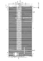
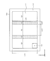
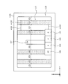
- FIG. 1 is a plan view showing a planar layout of the semiconductor device according to the first embodiment.
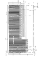
- FIG. 2 is a plan view showing a part of FIG. 1 in an enlarged manner.
- FIG. 3 is a plan view showing a part of FIG. 1 in an enlarged manner.
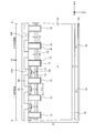
- FIG. 4 is a cross-sectional view showing a cross-sectional structure taken along line A-A 'in FIGS.
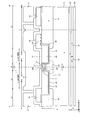
- FIG. 5 is a cross-sectional view showing a cross-sectional structure taken along line B-B 'in FIG.
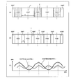
- FIG. 6 is a diagram showing the temperature amplitude according to the width of the IGBT region and the FWD region.
- FIG. 7 is a modification of the plan view showing the planar layout of the semiconductor device according to the second embodiment.
- FIG. 7 is a modification of the plan view showing the planar layout of the semiconductor device according to the second embodiment.
- FIG. 8 is a plan view showing a planar layout of the semiconductor device according to the third embodiment.
- FIG. 9 is a plan view showing a planar layout of the semiconductor device according to the fourth embodiment.
- FIG. 10 is a plan view showing a planar layout of the semiconductor device according to the fifth embodiment.
- FIG. 11 is a plan view showing an example of a planar layout of a conventional semiconductor device.
- FIG. 12 is a plan view showing an example of a planar layout of a conventional semiconductor device.
- n and p in the layer or region having n or p, it is meant that electrons or holes are majority carriers, respectively.
- + and-attached to n and p mean that the impurity concentration is higher and the impurity concentration is lower than that of the layer or region to which it is not attached, respectively.
- FIG. 1 is a plan view showing a planar layout of the semiconductor device according to the first embodiment.
- the planar layout is a planar shape and an arrangement configuration of each portion viewed from the front surface of the chip (the front surface of the semiconductor chip (semiconductor substrate) 10).
- the element structures of the IGBT and the FWD arranged in the IGBT region 1 and the FWD region 2 are not shown.
- FIG. 1 shows the semiconductor chip 10 having a substantially rectangular planar shape (the same applies to FIGS. 8 to 10), the planar shape of the semiconductor chip 10 may be square.
- FIGS. 2 and 3 are plan views showing a part of FIG. 1 in an enlarged manner.
- FIGS. 2 and 3 in order to clarify the arrangement of the first and second gate trenches 31 and 32 arranged in the IGBT region 1 and the FWD region 2, gate insulating films in the first and second gate trenches 31 and 32. 46 and the interlayer insulating film 50 on the front surface of the chip are not shown.
- FIG. 2 shows the vicinity 13 of the boundary between the IGBT region 1 and the FWD region 2 on the side of the central portion 11 e of the active region 11.
- FIG. 3 shows IGBT region 1 and FWD region 2 in the vicinity 14 of the boundary between active region 11 and edge termination region 12.
- an IGBT insulated gate type bipolar transistor
- an FWD heat diode
- the RC-IGBT reverse conductive IGBT
- the RC-IGBT has the above-described structure, and has the IGBT region 1 and the FWD region 2 in the active region 11.
- the active region 11 is a region through which a current flows (is responsible for current driving) when in the on state.
- the active region 11 has, for example, a substantially rectangular planar shape.
- the periphery of the active area 11 is surrounded by an edge termination area 12.
- the edge termination region 12 is a region between the active region 11 and the chip end of the semiconductor chip 10, and originates from the n ⁇ -type drift region 41 (see FIGS. 4 and 5) of the active region 11 and the p-type base region 42. This is an area for letting the equipotential line escape to the edge termination area 12 and relaxing the electric field on the front side of the chip to maintain the withstand voltage (withstand voltage) of the entire chip.
- the breakdown voltage is a voltage when an electric field on the front surface side of the chip becomes strong and an avalanche current is generated.
- the edge termination area 12 is provided with a general pressure-resistant structure (not shown) such as, for example, a field limiting ring (FLR).
- the IGBT region 1 is a region in which the IGBT is disposed, and is a region of the active region 11 other than the FWD region 2. That is, the sum of the surface area of the IGBT region 1 and the surface area of the FWD region 2 is the surface area of the active region 11.
- 2 and 3 show a state in which a plurality of unit cells of IGBT (arrangement units of elements) are arranged in parallel in IGBT region 1 and a plurality of unit cells of FWD are arranged in parallel in FWD region 2 (see FIG. The same applies to 4, 5).
- the FWD area 2 is an area where the FWD is arranged.
- the FWD regions 2 have, for example, a rectangular planar shape, and a plurality of FWD regions 2 are disposed apart from each other.
- the number of FWD regions 2 may be determined by the ratio of the surface area of the IGBT region 1 to the FWD region 2 in the active region 11.
- the plurality of FWD regions 2 may be dispersed throughout the active region 11. The reason is as follows. As a feature of the RC-IGBT, the IGBT region 1 and the FWD region 2 are arranged adjacent to each other. Therefore, heat generation from IGBT region 1 and FWD region 2 can be shared respectively. Thereby, the heat generation can be suppressed more than the IGBT region 1 and the FWD region 2 alone.
- the FWD region 2 has a high current density because the surface area can be narrowed compared to the IGBT region 1.
- the heat generation is shared by the structure of this RC-IGBT, a heat generation difference occurs depending on the width and the number of IGBT regions 1 and FWD regions 2, and there is a problem that the temperature of the semiconductor chip 10 tends to rise. Therefore, by arranging the plurality of FWD regions 2 in a distributed manner, heat generation in each FWD region 2 can be suppressed as compared to the case where one FWD region 2 is disposed.
- FIG. 6 is a diagram showing the temperature amplitude according to the width of the IGBT region and the FWD region.
- FIG. 6 shows the temperature amplitude according to the width of the IGBT region 1 and the FWD region 2.
- FIG. 6A shows the case where the width S of the IGBT region 1 is wider than the width of the FWD region 2.
- FIG. 6B shows the case where the width S of the IGBT region 1 is smaller than the width of the FWD region 2.
- FIG. 6 (c) shows the temperatures of FIG. 6 (a) and FIG. 6 (b).
- the dotted lines in the diagrams of FIGS. 6A and 6B indicate the positions of dotted lines in FIG. 6C.
- the temperature rises at the central portion of the FWD region 2 and the temperature tends to lower at the central portion of the IGBT region 1.
- the distance between the FWD regions 2 at this time (the width S of the IGBT region 1) is preferably 50% or more of the width of the FWD regions 2.
- the width S of the IGBT region 1 is narrowed, the snapback phenomenon of the conduction loss is likely to occur.
- the chip size of the semiconductor chip 10 is fixed, and if it is not desired to change the surface area ratio between the IGBT region 1 and the FWD region 2, the number of FWD regions 2 can not be increased. Therefore, by arranging the IGBT regions 1 and the FWD regions 2 as described above (see FIG. 1), the number of FWD regions 2 in the semiconductor chip 10 can be increased.
- the width of the FWD region 2 may be narrowed and the area thereof may be used to increase the number of the FWD regions 2.
- the plurality of FWD regions 2 be arranged at equal intervals.
- the reason is as follows. Since the IGBT and the FWD operate alternately, the timing of heat generation in the IGBT region 1 and the FWD region 2 is shifted by one cycle. Therefore, by arranging the plurality of FWD regions 2 at substantially equal intervals, heat is easily dispersed between the IGBT region 1 and the FWD region 2, and the heat generation of the entire semiconductor chip 10 is achieved by the semiconductor chip 10. It is possible to make it substantially uniform in the plane of.
- FWD region 2 be disposed on the boundary side between active region 11 and edge termination region 12 as much as possible by shortening length L 2 thereof.
- a polysilicon layer 35 is disposed on the front surface of the semiconductor chip 10 so as to cover an end portion on the edge termination region 12 side of the second gate trench 32 disposed in the FWD region 2 as described later. Therefore, unevenness due to the polysilicon layer 35 is generated on the element surface (the surface of the front surface electrode 51 described later: see FIG. 4).
- the front surface electrode 51 may be cracked or cracked.
- the FWD region 2 on the boundary side between the active region 11 and the edge termination region 12 and to place the unevenness due to the polysilicon layer 35 as outward as possible.
- the flat surface of the central portion (the central portion 11 e of the active region 11) of the semiconductor chip 10 to which the bonding wire is bonded can be expanded. Therefore, the diameter (diameter) of the bonding wire can be increased, and the contact resistance can be reduced.
- the plurality of FWD regions 2 form the outer periphery of active region 11 orthogonal to the sides 11 a and 11 b from a pair of opposite sides (long sides) 11 a and 11 b forming the outer periphery of active region 11. It is arranged in a striped planar layout extending in parallel to another pair of opposite sides (short sides) 11 c and 11 d toward the central portion 11 e of the active region 11.
- Each side 11 a to 11 d of the active region 11 is a boundary between the active region 11 and the edge termination region 12.
- the long sides of the active region 11 arranged in a substantially rectangular planar shape are referred to as sides 11a and 11b, and the short sides are referred to as sides 11c and 11d.
- the FWD area 2 on one side 11a side and the FWD area 2 on the other side 11b side are alternately arranged, and the FWD area 2 is formed in stripes. It does not face the extending direction (which indicates the longitudinal direction of the stripe; hereinafter referred to as the first direction) X. Therefore, even if a plurality of FWD regions 2 are dispersedly arranged in active region 11, all gate electrodes (not shown) arranged in a stripe planar layout in IGBT region 1 are gate trenches, as described later. It can be connected to a gate runner (not shown) at the end (not shown).
- the number of FWD regions 2 in contact with one pair of opposite sides 11a and 11b be the same. The reason is that when the bonding wire is connected to the center of the semiconductor chip 10, if the number of the FWD regions 2 is different, current concentration tends to occur in the smaller FWD region 2 and the heat dissipation may be deteriorated. It is because there is.
- Each FWD region 2 has a length L2 (length extending in the first direction X (longitudinal direction)) L2 which does not reach the central portion 11e of the active region 11 from the sides 11a and 11b of the active region 11. Preferably, it extends in the direction X. That is, the length L2 of each FWD region 2 is shorter than half the length L1 of the sides 11c and 11d of the active region 11 parallel to the stripes of the FWD region 2 (L2 ⁇ L1 / 2). In this case, the FWD region 2 on one side 11 a of the active region 11 and the FWD region 2 on the other side 11 b face in a direction Y (hereinafter referred to as a second direction) orthogonal to the first direction X. do not do.
- a direction Y hereinafter referred to as a second direction
- each FWD region 2 by shortening the length L2 of each FWD region 2, the portion 1a of the IGBT region 1 sandwiched between the FWD regions 2 on one side 11a of the active region 11 and the other side 11b
- the portion 1b sandwiched between the FWD regions 2 is disposed at a distance D1 in a direction oblique to the first direction X.
- the FWD region 2 on one side 11 a of the active region 11 and the FWD region 2 on the other side 11 b are separated by a distance D 2 in a direction oblique to the first direction X.
- the distances D1 and D2 can be made longer than in the case where the FWD regions 2 face each other in the first direction X.
- the FWD when the IGBT is turned on by applying a gate voltage of 15 V or more which is a general gate threshold voltage of the IGBT, the FWD may also be turned on.
- the electron current of the FWD is drawn to the channel (n-type inversion layer) of the IGBT adjacent to the FWD, which causes problems such as deterioration of the forward characteristic of the FWD.
- Such mutual interference at the boundary between the IGBT and the FWD is more likely to occur as the width (length parallel to the second direction Y (short direction)) w1 of the FWD region 2 is narrower. Therefore, the width w1 of the FWD region 2 is preferably, for example, 50 ⁇ m or more.
- the width (interval) w2 between the FWD regions 2 adjacent in the second direction Y is preferably equal to or greater than the width w1 of the FWD region 2 (w2 2 w1). The reason is that when the width w2 between the FWD regions 2 adjacent in the second direction Y is smaller than the width w1 of the FWD region 2, the conductivity modulation is delayed due to the snapback phenomenon.
- the front surface electrode pad (not shown) and the gate pad (electrode pad) 3 are disposed apart from each other.
- the front surface electrode pad covers, for example, the front surface of the semiconductor chip 10 over the entire area of the active region 11 other than the portion covered by the gate pad 3.
- FIG. 1 shows the case where gate pad 3 is arranged at one vertex of active region 11 at the boundary between active region 11 and edge termination region 12.
- the front surface electrode pad has, for example, a substantially L-shaped planar shape facing two continuous sides of the gate pad 3 having a substantially rectangular planar shape.
- first and second gate trenches 31 and 32 are disposed in the IGBT region 1 and the FWD region 2 respectively.
- the first and second gate trenches 31 and 32 are arranged in stripes parallel to the first direction X and on stripes of the same pitch, separated from each other.
- the first and second gate trenches 31 and 32 are disposed apart from each other. Further, end portions of the first and second gate trenches 31 and 32 adjacent to each other in the first direction X face each other in the first direction X with the boundary region 15 between the IGBT region 1 and the FWD region 2 interposed therebetween.
- the boundary region 15 is a region between the first and second gate trenches 31 and 32 in the first direction X, and is a region disposed between the active regions 11 for holding a breakdown voltage.
- Each of the first gate trenches 31 constituting a stripe planar layout parallel to the first direction X may have a linear planar shape parallel to the first direction X, or may be parallel to the first direction X
- the annular planar shape which connected the edge parts of the adjacent linear part may be provided.
- Each of the second gate trenches 32 constituting a stripe planar layout parallel to the first direction X may have a linear planar shape parallel to the first direction X, or may be parallel to the first direction X.
- the annular planar shape which connected the edge parts of the adjacent linear part may be provided.
- the FWD regions 2 arranged apart from each other by the distance D2 (see FIG. 1) across the central portion 11e of the active region 11 are at least a first gate trench 31 having a linear planar shape in the second direction Y.
- first gate trenches 31 and one of the first gate trenches 31 having an annular planar shape are opposed to each other. That is, at least two first gate trenches 31 having a linear planar shape or one first gate trench having an annular planar shape between the second gate trenches 32 closest to the IGBT region 1 in the second direction Y 31 is placed.
- the p + -type contact region 33 has a linear planar shape parallel to the second direction Y.
- the p + -type contact region 33 is a contact in which a contact (electrical contact portion) with the front surface electrode 51 (see FIG. 4) of the emitter potential is formed in the boundary region 15 between the IGBT region 1 and the FWD region 2 Form a hole 34a.
- first and second gate trenches 31 and 32 there are contact holes 34b with the front surface electrode 51, respectively. It is provided in a linear planar shape extending in the first direction X.
- first and second gate trenches 31 and 32 have an annular planar shape, a region surrounded by the annular planar shapes first and second gate trenches 31 and 32 (first and second gate trenches 31 and 32
- the contact hole 34 b is also provided in a linear planar shape extending in the first direction X).
- the end on the edge termination region 12 side of the first and second gate trenches 31 and 32 extends to the edge termination region 12.
- the end on the edge termination region 12 side of the first gate trench 31 extends, for example, outside the end on the edge termination region 12 side of the second gate trench 32 (on the end side of the semiconductor chip 10) .
- a polysilicon (poly-Si) layer 35 of the emitter potential of the IGBT is provided so as to cover the end of the second gate trench 32 on the edge termination region 12 side.
- the polysilicon layer 35 is provided, for example, in a linear planar shape extending in the second direction Y so as to face the end on the edge termination region 12 side of all the second gate trenches 32. In FIG. 3, the polysilicon layer 35 is shown by a fine broken line.
- the polysilicon layer 35 is electrically connected to the second gate electrode 49 at the end on the edge termination region 12 side of the second gate trench 32.
- the polysilicon layer 35 is electrically connected to a p-type well region 62 described later via a contact hole 34c in the vicinity of the edge on the edge termination region 12 side of the second gate trench 32 (see FIG. 5). ).
- the contact holes 34 c are provided, for example, in a linear planar shape extending in the second direction Y so as to face the end on the edge termination region 12 side of all the second gate trenches 32.
- a plurality of (three in FIG. 5) contact holes 34c may be arranged in a striped planar layout extending in the second direction Y.
- a plug made of, for example, tungsten (W) is embedded in the contact hole 34c. Therefore, the width of the contact hole 34c is preferably narrow.
- a gate runner 36 of the gate potential of the IGBT is provided so as to cover an end portion on the edge termination region 12 side of the first gate trench 31.
- the gate runner 36 is formed of, for example, polysilicon.
- the gate runner 36 is disposed outside the polysilicon layer 35 of the emitter potential and away from the polysilicon layer 35, and surrounds the periphery of the active region 11.
- the first gate electrode 47 inside the first gate trench 31 is electrically connected to the gate runner 36 at an end portion on the edge termination region 12 side of each first gate trench 31.
- the gate runner 36 is electrically connected to the gate pad 3 (see FIG. 1). In FIG. 3, the gate runner 36 is shown by a broken line which is rougher than the polysilicon layer 35.
- FIG. 4 is a cross-sectional view showing a cross-sectional structure taken along line A-A 'in FIGS.
- FIG. 5 is a cross-sectional view showing a cross-sectional structure taken along line B-B 'in FIG.
- the cutting line B1-B1 ', the cutting line B3-B3' of FIG. 3 and the cutting line B2-B2 'of FIG. 2 are parts of the cutting line B-B' of FIG.
- the cross-sectional structure of the cutting line A-A 'passing in parallel with the second direction Y along the boundary 16 between the IGBT region 1 and the FWD region 2 will be described with reference to FIG.
- the IGBT region 1 and the FWD region 2 are arranged in parallel in the second direction Y in the n ⁇ type semiconductor chip (semiconductor substrate) 10 to be the n ⁇ type drift region 41.
- a p-type base region 42 is provided in the surface layer on the front surface of the semiconductor chip 10.
- the portion other than the region 54 is the n ⁇ -type drift region 41.
- an n + -type emitter region 43 and a p + -type contact region 44 are selectively provided in contact with each other.
- An n-type CS region 45 is provided between the p-type base region 42 and the n ⁇ -type drift region 41.
- the impurity concentration of the n-type CS region 45 is higher than the impurity concentration of the n ⁇ -type drift region 41 and lower than the impurity concentration of the n + -type emitter region 43.
- the n-type CS region 45 has a function of accumulating holes when the IGBT is on and reducing the surface resistance. Therefore, by providing the n-type CS region 45, the on-resistance can be improved.
- the first gate trench 31 penetrates the n + -type emitter region 43, the p-type base region 42 and the n-type CS region 45 in the depth direction Z from the front surface of the semiconductor chip 10 to the n ⁇ -type drift region 41. Reach.
- the depth direction Z is a direction from the front surface to the back surface of the semiconductor chip 10.
- a first gate electrode 47 is provided via a first gate insulating film 46.
- the first gate electrode 47 and the n + -type emitter region 43 face each other with the first gate insulating film 46 on the side wall of the first gate trench 31 interposed therebetween.
- the n + -type emitter region 43 is disposed only in the portion along the sidewall of the first gate trench 31
- the p + -type contact region 44 is disposed in the central portion between adjacent first gate trenches 31.
- the n + -type emitter region 43 and the p + -type contact region 44 have a linear planar shape extending in the first direction X along the sidewall of the first gate trench 31.
- the n + -type emitter regions 43 and the p + -type contact regions 44 may be alternately and repeatedly arranged in the first direction X between the adjacent first gate trenches 31.
- the n + -type emitter region 43 and the p + -type contact region 44 face the first gate electrode 47 with the first gate insulating film 46 on the side wall of the first gate trench 31 interposed therebetween.
- the first gate trench 31 penetrates the n + -type emitter region 43, the p + -type contact region 44, the p-type base region 42 and the n-type CS region 45 in the depth direction Z from the front surface of the semiconductor chip 10 Then the n - type drift region 41 is reached.
- the p + -type contact region 33 is a contact in which a contact (electrical contact portion) with the front surface electrode 51 (see FIG. 4) of the emitter potential is formed in the boundary region 15 between the IGBT region 1 and the FWD region 2 It is formed to be exposed in the hole 34a.
- a p-type base region 42 described later is disposed on the lower surface of the p + -type contact region 33. Further, an n-type CS region 45 described later is disposed on the lower surface of the p-type base region 42.
- Front surface electrode 51 via the contact hole 34b, the contact n + -type emitter region 43 and p + -type contact region 44, electrically connected to these n + -type emitter region 43 and p + -type contact region 44 It is done.
- the front surface electrode 51 is electrically insulated from the first gate electrode 47 by the interlayer insulating film 50.
- the front surface electrode 51 functions as a front surface electrode pad.
- the p-type base region 42, the interlayer insulating film 50 and the front surface electrode 51 are provided from the IGBT region 1 to the FWD region 2. In the FWD region 2, the n + -type emitter region 43 and the p + -type contact region 44 are not provided.
- the p-type base region 42 functions as a p-type anode region, and the front surface electrode 51 doubles as an anode electrode.
- a second gate trench 32 is provided in the FWD region 2.
- the second gate trench 32 penetrates the p-type base region 42 and the n-type CS region 45 in the depth direction Z from the front surface of the semiconductor chip 10 to reach the n ⁇ -type drift region 41.
- the arrangement of the second gate trenches 32 is, for example, similar to the arrangement of the first gate trenches 31 in the IGBT region 1.
- a second gate electrode 49 is provided inside the second gate trench 32 via a second gate insulating film 48.
- the second gate electrode 49 is electrically separated from the first gate electrode 47. That is, in the FWD region 2, like the p-type base region 42, the first gate trench 31, the first gate insulating film 46 and the first gate electrode 47 in the IGBT region 1, the p-type base region 42 and the second gate trench A second gate insulating film 48 and a second gate electrode 49 are provided.
- the front surface electrode 51 is in contact with the p-type base region 42 via the contact hole 34 b and is electrically connected to the p-type base region 42.
- the front surface electrode 51 is in contact with a p-type well region 62 described later via a contact hole 34 c and is electrically connected to the p-type well region 62.
- the front surface electrode 51 is electrically connected to the second gate electrode 49, and fixes the second gate electrode 49 to the emitter potential of the IGBT.
- the front surface electrode 51 is electrically insulated from the first gate electrode 47 by the interlayer insulating film 50.
- an n-type FS region 52 is provided from the IGBT region 1 to the FWD region 2.
- the n-type FS region 52 has a function of suppressing the extension of the depletion layer extending from the pn junction of the p-type base region 42 and the n ⁇ -type drift region 41 when the IGBT is off.
- p + -type collector region 53 is formed in the IGBT region 1, the FWD region 2 n + A mold cathode region 54 is provided.
- the p + -type collector region 53 and the n + -type cathode region 54 are in contact with, for example, the n-type FS region 52. Further, the p + -type collector region 53 and the n + -type cathode region 54 are in contact with each other and arranged in parallel in the direction parallel to the back surface of the semiconductor chip 10.
- Back electrode 55 is in contact with p + -type collector region 53 and n + -type cathode region 54 is provided on the entire back surface of the semiconductor chip 10 is electrically connected to these p + -type collector region 53 and n + -type cathode region 54 ing.
- the back surface electrode 55 doubles as a collector electrode and a cathode electrode.
- FIG. 5 is a cross-sectional view taken along a line BB ′ parallel to the first direction X, in the boundary region 15 between the IGBT region 1 and the FWD region 2 and the first and second gate trenches 31 and 32.
- a p-type base region 42 is provided in the surface layer on the front surface of the semiconductor chip 10.
- an n-type CS region 45 is provided between the p-type base region 42 and the n ⁇ -type drift region 41.
- ap + -type contact region 33 is selectively provided inside the p-type base region 42.
- a p-type well region 61 of an emitter potential may be provided in the boundary region 15 between the IGBT region 1 and the FWD region 2 as shown by a broken line.
- the width w4 of the boundary region 15 between the IGBT region 1 and the FWD region 2 may be wider than the mesa width w3.
- the p-type well region 61 extends from the front surface of the semiconductor chip 10 to a position deeper than the first and second gate trenches 31 and 32.
- the p-type well region 61 is provided from the side wall to the bottom of the opposite end of the first and second gate trenches 31 and 32 across the boundary region 15, and the bottom corners of the first and second gate trenches 31 and 32. Cover the department.
- the bottom corner portions of the first and second gate trenches 31 and 32 are boundaries between the side walls and the bottom of the first and second gate trenches 31 and 32.
- a p-type well region 62 is provided on the surface layer of the front surface of the semiconductor chip 10 outside the first and second gate trenches 31 and 32 so as to surround the active region 11. ing.
- the p-type well region 62 extends from the front surface of the semiconductor chip 10 to a position deeper than the first and second gate trenches 31 and 32.
- the p-type well region 62 is provided from the side wall to the bottom surface of the end on the edge termination region 12 side of the first and second gate trenches 31 and 32 and covers the bottom corner portion.
- a breakdown voltage structure such as FLR is provided outside the p-type well region 62 in the surface layer on the front surface of the semiconductor chip 10.
- the polysilicon layer 35 of the emitter potential and the gate runner 36 of the gate potential are provided apart from each other on the front surface of the semiconductor chip 10.
- the polysilicon layer 35 extends outward from the end of the second gate trench 32 on the side of the edge termination region 12, and for example, the second gate insulating film 48 (or the interlayer insulating film 50) on the front surface of the semiconductor chip 10. And a portion of the p-type well region 62 in the depth direction Z.
- the polysilicon layer 35 is in contact with the second gate electrode 49 inside the second gate trench 32 and is electrically connected to the second gate electrode 49.
- the polysilicon layer 35 is in contact with the p-type well region 62 via the contact hole 34 c penetrating the second gate insulating film 48 in the depth direction Z, and is electrically connected to the p-type well region 62.
- the gate runner 36 opposes the p-type well region 62 in the depth direction Z with, for example, the first and second gate insulating films 46 and 48 (or the interlayer insulating film 50) on the front surface of the semiconductor chip 10.
- the polysilicon layer 35 is in contact with the second gate electrode 49 inside the second gate trench 32, is electrically connected to the second gate electrode 49, and through the surface electrode 51 and the contact hole 34a. , And is electrically connected to the p + -type contact region 33 of the boundary region 15.
- the gate runner 36 covers a portion of the end on the edge termination region 12 side of the first gate trench 31 extending to the edge termination region 12.
- the gate runner 36 is in contact with the first gate electrode 47 inside the first gate trench 31 at a portion covering the end on the edge termination region 12 side of the first gate trench 31 and is electrically connected to the first gate electrode 47. It is connected.
- the IGBT region 1 is a region from the end on the inner side (the central portion side of the active region 11) of the gate runner 36 to the boundary region 15 between the IGBT region 1 and the FWD region 2.
- the FWD region 2 is a region from the inner end of the polysilicon layer 35 to the boundary region 15 between the IGBT region 1 and the FWD region 2.
- the front surface electrode 51 covers the whole of the active region 11 and the boundary region 15 between the IGBT region 1 and the FWD region 2. Further, the front surface electrode 51 extends to the edge termination region 12 and covers the polysilicon layer 35 via the interlayer insulating film 50. The front surface electrode 51 is in contact with the polysilicon layer 35 via a contact hole penetrating the interlayer insulating film 50 in the depth direction, and is electrically connected to the polysilicon layer 35.
- the gate pad 3 is provided on the gate runner 36 via the interlayer insulating film 50. The gate pad 3 is in contact with the gate runner 36 through a contact hole penetrating the interlayer insulating film 50 in the depth direction, and is electrically connected to the gate runner 36.
- the p + -type collector region 53 is provided from the IGBT region 1 to the boundary region 15 between the IGBT region 1 and the FWD region 2.
- the p + -type collector region 53 extends from the boundary region 15 between the IGBT region 1 and the FWD region 2 to the FWD region 2 and extends in the depth direction Z at the end of the second gate trench 32 on the boundary region 15 side. It is preferable to face each other. The reason is that since the diffusion of electrons in the n + -type cathode region 54 in the FWD region 2 tends to generate holes from the p + -type contact region 33 in the IGBT region 1, the SW loss tends to be deteriorated.
- a plurality of FWD regions are disposed apart from each other in the active region, and IGBT regions sandwiched between the plurality of FWD regions are defined as continuous regions.
- the FWD region is arranged in a stripe planar layout extending from the boundary between the active region and the edge end region in a direction orthogonal to the boundary and ending near the central portion of the active region, A portion other than the FWD region is an IGBT region.
- the FWD regions are arranged in the same number across the IGBT regions.
- the width of the FWD region can be increased to a predetermined width while maintaining the surface area ratio between the IGBT region and the FWD region, and the FWD region disposed in the active region The number can be increased.
- the width or number of FWD regions is obtained if priority is given to the surface area ratio between the IGBT region and the FWD region.
- the number is limited.
- the FWD regions can be arranged with a predetermined width and a predetermined number, and therefore the degree of freedom in design is higher than in the conventional structure.
- the width of the FWD region to 50 ⁇ m or more, the deterioration of the forward characteristic of the FWD at the time of applying a gate voltage of 15 V or more which is a general gate threshold voltage of the IGBT is within the allowable range. it can. Further, for example, by setting the width of the FWD region to 400 ⁇ m or more, it is possible to prevent the deterioration of the forward characteristic of the FWD when applying a gate voltage of 15 V or more which is a general gate threshold voltage of the IGBT.
- the heat dissipation of FWD can be improved by increasing the number of FWD regions.
- the chip size is the same and the surface area ratio is the same as the IGBT area and the FWD area, the amount of heat generation of the entire semiconductor chip can be reduced by about 20% to 30% as compared with the conventional structure.
- the arrangement in which the IGBT region and the FWD region are adjacent to each other is smaller than in the conventional structure. For example, as shown in FIG. 1, when the FWD region is disposed with a length not reaching the central portion of the active region from the boundary between the active region and the edge end region, only the IGBT is disposed at the central portion of the active region . Therefore, mutual interference between the IGBT and the FWD can be suppressed.
- the FWD region on one side and the FWD region on the other side of the pair of opposite sides of the active region are alternately arranged to surround the active region.
- the gate electrode of the IGBT can be connected to the surrounding gate runner at the position of the end of each first gate trench. Therefore, the connection between the gate electrode of the IGBT and the gate runner is easy.
- FIG. 7 is a plan view showing a planar layout of the semiconductor device according to the second embodiment.
- the semiconductor device according to the second embodiment differs from the semiconductor device according to the first embodiment in that the length L2 of the FWD region 2 is shortened.
- FIG. 7A shows a state in which the FWD regions 2 are arranged to face each other in the first direction X.
- FIG. 7B shows a state in which the FWD regions 2 are arranged so as not to face each other in the first direction X, as in the first embodiment.
- FIG. 7C shows a state in which the FWD regions 2 are arranged to face each other in the first direction X, as in FIG. 7A. Furthermore, in the FWD regions 2 arranged at both ends (ends in the second direction Y) of the active region 11, the facing FWD regions 2 are arranged so as to be connected in the longitudinal direction (first direction X).
- the number of FWD regions 2 is determined by the surface area ratio between IGBT region 1 and FWD region 2.
- the sectional structure of the IGBT region 1 and the FWD region 2 is the same as that of the first embodiment except that the FWD region 2 is not provided below the front surface electrode 51 as described later.
- the FWD region 2 Since the length L2 of the FWD region 2 is short, the distance D1 between the portions of the IGBT region separated in the oblique direction with respect to the first direction X, and in the oblique direction with respect to the first direction X The distance D2 between the FWD regions 2 can be made longer. Therefore, the FWD region 2 is not provided below the front surface electrode 51 in the central portion of the semiconductor chip 10.
- a bonding wire (not shown) is connected to the front surface electrode 51.
- the bonding surface of the bonding wire connected to the front surface electrode 51 and the FWD region 2 can be separated by a fixed distance. By separating the bonding surface of the bonding wire and the FWD region 2 at a constant distance, heat generation in the FWD region 2 can be suppressed.
- the sheet resistance of the front surface electrode 51 between the bonding surface of the bonding wire and the FWD region 2 becomes large, so the FWD region The heat dissipation deterioration due to the current concentration of 2 can be further prevented.
- the same effect as that of the first embodiment can be obtained. Further, according to the second embodiment, the heat generation in the FWD region can be further suppressed by shortening the length of the FWD region.
- FIG. 8 is a plan view showing a planar layout of the semiconductor device according to the third embodiment.
- the semiconductor device according to the third embodiment is a semiconductor device according to the first embodiment applied to an IGBT (sense IGBT) for detecting and controlling a current.
- IGBT sense IGBT
- a current sense portion (not shown) is a vertical MOSFET (Metal Oxide Semiconductor Field Effect Transistor), and has a function of detecting an over current (OC) flowing through the IGBT in the IGBT region 71.
- the source electrode of the current sensing portion doubles as a sense pad (hereinafter referred to as an OC pad) 76 for current sensing.
- the current sense portion is disposed, for example, immediately below the OC pad 76 (a portion facing in the depth direction Z).
- the temperature sensing unit (not shown) is a diode and has a function of detecting the temperature of the IGBT in the IGBT region 1 using the temperature characteristic of the diode.
- the anode electrode and the cathode electrode of the temperature sensing unit double as the anode pad 74 and the cathode pad 75, respectively.
- the temperature sensing unit is disposed, for example, immediately below the anode pad 74 and the cathode pad 75.
- the over voltage protection unit (not shown) is a diode, and protects the IGBT in the IGBT region 71 from over voltage (OV) such as a surge, for example.
- the anode electrode of the overvoltage protection portion doubles as a sense pad (hereinafter referred to as an OV pad) 77 for overvoltage protection.
- the overvoltage protection unit is disposed, for example, immediately below the OV pad 77.
- the temperature sensing unit and the overvoltage protection unit may be, for example, a lateral diode formed of a pn junction of a p-type polysilicon layer and an n-type polysilicon layer provided on the semiconductor chip 10 via an insulating film. Alternatively, it may be a vertical diode formed of a pn junction of a p-type diffusion region and an n-type diffusion region provided inside the semiconductor chip 10.
- Electrode pads such as front surface electrode pad (not shown) and gate pad 73 of IGBT, anode pad 74 and cathode pad 75 of temperature sensing part, OC pad 76 of current sensing part, OV pad 77 of over voltage protection part
- the IGBT region 71 is disposed on the front surface of the semiconductor chip 10 at a distance from the FWD region 72.
- the gate pad 73, the anode pad 74, and the cathode pad 75 along one side 11b of the active region 11 orthogonal to the stripes of the FWD region 72 in the vicinity of the boundary with the edge termination region 12 of the active region 11.
- the OC pad 76 is arranged, and the OV pad 77 is arranged in the vicinity of the central portion 11 e of the active region 11, but the arrangement of these electrode pads can be variously changed.
- the configurations of the IGBT region 71 and the FWD region 72 are the same as those of the first embodiment except that the arrangement of the FWD region 72 and the gate pad 73 and the planar shape of the front surface electrode pad (not shown) are different.
- the front surface electrode 51 (see FIG. 4) of the IGBT in the IGBT region 71 is electrically connected to the cathode electrode of the temperature sensing unit and the anode electrode of the over voltage protection unit.
- the FWD regions 72 are arranged, for example, in a stripe planar layout extending from the other side 11a of the active area 11 opposite the one side 11b where the gate pad 73 etc. are arranged to the central portion 11e of the active area 11, It terminates near the central portion 11 e of the active region 11.
- the IGBT region 71 is a region other than the FWD region 72 of the active region 11 as in the first embodiment.
- the width w101 'of the IGBT region 101 is narrowed at the portion where the gate pad 103 and the sense pads 104 to 107 are disposed, which may hinder the IGBT operation.
- the width L of the IGBT region 71 is secured widely by shortening the length L 2 of the FWD region 72 and setting the FWD region 72 in a planar layout terminated in the vicinity of the central portion 11 e of the active region 11. As a result, deterioration of the IGBT characteristics can be prevented.
- the length L2 of the FWD region 72 is shortened, and the FWD region 72 is terminated in the vicinity of the central portion 11 e of the active region 11 to form a planar layout.
- the FWD area 72 can be disposed apart from the area 77. Thereby, a wide FWD region 72 of width w1 can be arranged. By widening the width w1 of each FWD region 72, the thermal resistance in each FWD region 72 decreases, and deterioration of the forward characteristics and reverse recovery characteristics of the FWD can be prevented.
- the same effect as that of the first embodiment can be obtained. Further, according to the third embodiment, the deterioration of the IGBT characteristics and the FWD characteristics can be prevented.
- FIG. 9 is a plan view showing a planar layout of the semiconductor device according to the fourth embodiment.
- the semiconductor device according to the fourth embodiment is different from the semiconductor device according to the third embodiment in that the width w1 of each FWD region 72 is narrowed to improve the heat dissipation of each FWD region 72.
- the width w1 of each FWD region 72 is narrowed, for example, by increasing the number of FWD regions 72, the total surface area of the FWD regions 72 has a predetermined size (for example, about the same as the total surface area of the FWD regions 102 of the conventional structure) Can be maintained.
- Electrode pads such as front surface electrode pad (not shown) and gate pad 73 of IGBT, anode pad 74 and cathode pad 75 of temperature sensing part, OC pad 76 of current sensing part, OV pad 77 of over voltage protection part , Or may extend from IGBT region 71 to FWD region 72.
- a portion of the FWD region 72 covered with the electrode pad is shown by a broken line.
- the temperature sense unit and the overvoltage protection unit may be vertical diodes configured using a part of the FWD of the FWD region 72.
- the width of the FWD region is narrowed, and the FWD regions are dispersedly arranged in a plurality, whereby each FWD region is arranged as compared to the case where one FWD region is arranged in the active region.
- the heat generation of the FWD region can be improved.
- FIG. 10 is a plan view showing a planar layout of the semiconductor device according to the fifth embodiment.
- the semiconductor device according to the fifth embodiment differs from the semiconductor device according to the first embodiment in a part of the FWD region 82 on the side 11 a of the active region 11 and in the FWD region 82 on the side 11 b of the other. A part is a point opposite to the second direction Y.
- the IGBT region 81 is a region other than the FWD region 82 of the active region 11 as in the first embodiment.
- each FWD region 82 is opposed to the other side 11b (opposite the side 11a (or the side 11b) beyond the central portion 11e of the active region 11). Or it extends to the side 11a) side.
- the distance w5 between the end on the other side 11b (or side 11a) side of the FWD region 82 and the other side 11b (or side 11a) is preferably equal to or greater than the width w1 of the FWD region 82 (w5) W w1).
- the part on the other side 11 b side of the FWD area 82 on the side 11 a side of the active area 11 and the part on the other side 11 a side of the FWD area 82 on the other side 11 b face in the second direction Y Do.
- the fifth embodiment even if the length of the FWD region is increased, if one end of the FWD region does not reach the boundary between the active region and the edge end region, the operation is performed.
- the same effects as those of the first to third aspects can be obtained.
- the FWD region is arranged in a stripe planar layout parallel to the short side of the substantially rectangular active region, but in the substantially rectangular active region, The FWD regions may be arranged in a stripe planar layout parallel to the long side. Also, the number of FWD regions may be even or odd.
- the small chip IGBT is described as an example in each of the embodiments described above, the invention can be applied to the case where the chip size is large, and the same effect can be obtained when the surface area of the FWD region is reduced. Play. Further, the present invention is similarly applicable even when the conductivity type (n type, p type) is reversed.
- the semiconductor device according to the present invention is useful for a semiconductor device having a withstand voltage of 600 V or more, which is used for power converters such as inverters, power supply devices such as various industrial machines, and igniters of automobiles. It is suitable for RC-IGBTs used for inverters, IPM (Intelligent Power Module), etc.
Landscapes
- Metal-Oxide And Bipolar Metal-Oxide Semiconductor Integrated Circuits (AREA)
Abstract
半導体チップ(10)の活性領域(11)に、IGBTを配置したIGBT領域(1)と、当該IGBTに逆並列に接続されたFWDを配置したFWD領域(2)と、が設けられる。FWD領域(2)は、活性領域(11)に互いに離して複数配置される。IGBT領域(1)は、複数のFWD領域(2)の間に挟まれた連続した領域である。IGBT領域(1)およびFWD領域(2)には、それぞれ半導体チップ(10)のおもて面に平行で、かつ同一の第1方向(X)に延びるストライプ状のレイアウトに第1,2ゲートトレンチ(31,32)が配置される。FWD領域(2)のFWDの第2ゲートトレンチ(32)は、IGBT領域(1)のIGBTの第1ゲートトレンチ(31)と離して配置される。この構造を備えることによって、素子特性の悪化を防止することができ、半導体チップ(10)の放熱性を向上させることができ、かつ設計自由度を向上させることができる。
Description
この発明は、半導体装置に関する。
従来、IGBT(Insulated Gate Bipolar Transistor:絶縁ゲート型バイポーラトランジスタ)と、FWD(Free Wheeling Diode:還流ダイオード)と、を同一の半導体チップに内蔵して一体化した逆導通型IGBT(RC-IGBT:Reverse Conducting IGBT)が公知である。RC-IGBTでは、FWDが配置された領域(以下、FWD領域とする)は、半導体チップのおもて面から見てストライプ状のレイアウトに配置される。
従来のRC-IGBTのFWD領域の、半導体チップのおもて面から見たレイアウト(以下、平面レイアウトとする)について説明する。図11,12は、従来の半導体装置の平面レイアウトの一例を示す平面図である。図11には、半導体チップ110aにIGBTおよびFWDを配置した一例(以下、小チップIGBTとする)である。図12は、電流とチップ温度の検出・制御を行うためのIGBT(以下、センスIGBTとする)と同一の半導体チップ110bにFWDを配置した一例である。
図11,12に示す従来の半導体装置は、活性領域111にIGBT領域101とFWD領域102とを有する。IGBT領域101は、IGBTが配置された領域であり、活性領域111のうち、FWD領域102以外の領域である。IGBT領域101の表面積とFWD領域102の表面積との総和が活性領域111の表面積となる。FWD領域102はストライプ状のレイアウトに配置され、その両端部は活性領域111とエッジ終端領域112との境界に達している。すなわち、FWD領域102の長さ(長手方向の長さ)L102は、略矩形状の平面形状の活性領域111の、FWD領域102のストライプの方向に平行な1辺の長さL101と略同じである。
FWD領域102により、IGBT領域101のIGBTの単位セル(素子の構成単位)は複数の領域に分離して配置されている。また、活性領域111には、ゲートパッド(電極パッド)103や、電流・温度センス用のセンスパッド104~107等の電極パッドが配置されている。図11には、活性領域111の1つの頂点付近にゲートパッド103を配置した場合を示す。図12には、活性領域111の、FWD領域102のストライプと直交する1辺に沿ってゲートパッド103およびセンスパッド104~106を配置し、かつ中央付近にセンスパッド107を配置した場合を示す。
従来のRC-IGBTとして、4つのダイオード領域がマトリクス状の平面レイアウトに配置され、当該4つのダイオード領域を囲むようにIGBT領域を配置した装置が提案されている(例えば、下記特許文献1(第0012段落、図1,2,8,10)参照。)。下記特許文献1では、IGBT領域のゲートトレンチとダイオード領域のゲートトレンチとが、同一ストライプ上に当該ストライプの延びる方向に互いに離してそれぞれストライプ状に配置され、その端部同士がp型ウェル層を介して対向している。
また、従来のRC-IGBTの別の一例として、短冊形状の複数のIGBT領域および複数のダイオード領域と直交するように、当該複数のIGBT領域と複数のダイオード領域との間に、活性領域として機能しない非活性領域を配置した装置が提案されている(例えば、下記特許文献2(第0067段落、第1,2図)参照。)。下記特許文献2では、ダイオードセル領域がストライプ状に延びる方向にダイオードセル領域同士が互いに離して配置され、その端部同士が非活性領域を介して対向している。
半導体チップ110aの温度上昇を抑制するためには、活性領域111に配置するFWD領域102の本数を多くすることでIGBT領域101とFWD領域102との温度差が無くなるので好ましい。しかしながら、従来のRC-IGBTでは、小チップIGBTとした場合(図11参照)、活性領域111にFWD領域102を1~2本程度しか配置することができない。このため、半導体チップの放熱性が悪くなるという問題がある。そこで、半導体チップの放熱性を最適化する場合、FWD領域102の面積を調整する際にFWD領域102の面積によっては、FWD領域102の幅w102を狭くし、FWD領域102の幅w102を狭くした面積分を、FWD領域102の本数を増やすことに用いる必要がある。しかしながら、FWD領域102の幅w102を狭くしすぎると、IGBTの一般的なゲート閾値電圧である15V以上のゲート電圧印加時にFWDの順方向特性が悪化するという問題がある。一方、チップサイズが大きい場合であっても、FWD領域102の面積を調整する際に、FWD領域102の幅w102を狭くする必要があり、小チップIGBTと同様の問題が生じる。
また、センスIGBTとした場合(図12参照)、ゲートパッド103にFWD領域102が接してしまうため、FWD領域102の平面レイアウトを工夫する必要がある。また、電極パッドを配置した部分でIGBT領域101の幅w101が狭くなる。かつ、小チップIGBTと同様に、FWD領域102の幅w102も狭い。このため、IGBTの電子電流がFWD領域102に抜けやすい構造となる等、IGBTとFWDとの境界で相互干渉が生じ、素子特性が悪化するという問題がある。
この発明は、上述した従来技術による問題点を解消するため、素子特性の悪化を防止する、または、半導体チップの放熱性を向上させることができる半導体装置を提供することを目的とする。さらに、上述した従来技術による問題点を解消するため、FWD領域の設計自由度を向上させることができる半導体装置を提供することを目的とする。
上述した課題を解決し、本発明の目的を達成するため、この発明にかかる半導体装置は、次の特徴を有する。半導体基板に、電流が流れる活性領域が設けられている。前記活性領域に、第1素子領域が設けられている。前記第1素子領域には、第1のトレンチゲート構造を有する第1素子が配置されている。前記活性領域に、第2素子領域が設けられている。前記第2素子領域には、第2のトレンチゲート構造を有する第2素子が配置されている。前記第1のトレンチゲート構造は、第1トレンチおよび第1ゲート電極を有する。前記第1トレンチは、前記半導体基板の第1主面側に設けられている。第1ゲート電極は、前記第1トレンチの内部に第1ゲート絶縁膜を介して設けられている。前記第2のトレンチゲート構造は、第2トレンチおよび第2ゲート電極を有する。前記第2トレンチは、前記半導体基板の第1主面側に、前記第1トレンチと離して設けられている。前記第2ゲート電極は、前記第2トレンチの内部に第2ゲート絶縁膜を介して設けられている。前記第2素子領域は、互いに離して複数配置されている。前記第1素子領域は、複数の前記第2素子領域の間に挟まれた連続した領域である。
また、この発明にかかる半導体装置は、上述した発明において、前記第2素子領域は、前記活性領域の外周寄りに配置されていることを特徴とする。
また、この発明にかかる半導体装置は、上述した発明において、複数の前記第2素子領域は、前記半導体基板の第1主面に平行で、かつ矩形状の平面形状を有する前記活性領域の外周を構成する1組の対辺それぞれからもう1組の対辺に平行な第1方向に延びるストライプ状のレイアウトに配置されている。前記活性領域の前記第1方向に対向する1組の対辺のうち、一方の辺側に配置された前記第2素子領域と、他方の辺側に配置された前記第2素子領域と、は前記第1方向と直交する第2方向に互い違いに配置されており、チップ中心ラインからのFWD本数を同数とすることを特徴とする。
また、この発明にかかる半導体装置は、上述した発明において、前記第2素子領域の前記第1方向の長さは、前記第2素子領域の前記第2方向の幅よりも長いことを特徴とする。
また、この発明にかかる半導体装置は、上述した発明において、隣り合う前記第2素子領域の間の幅は、前記第2素子領域の前記第2方向の幅以上であることを特徴とする。
また、この発明にかかる半導体装置は、上述した発明において、前記第2素子領域の前記第2方向の幅は、50μm以上であることを特徴とする。
また、この発明にかかる半導体装置は、上述した発明において、前記第1素子は、第1導電型の第1,3半導体領域、第2導電型の第2,4半導体領域、前記第1トレンチ、前記第1ゲート電極および第1,2電極を有する。前記第1半導体領域は、前記半導体基板に設けられている。前記第2半導体領域は、前記半導体基板の第1主面の表面層に、前記第1半導体領域に接して設けられている。前記第3半導体領域は、前記第2半導体領域の内部に選択的に設けられている。前記第1トレンチは、前記第3半導体領域および前記第2半導体領域を貫通して前記第1半導体領域に達する。前記第4半導体領域は、前記半導体基板の第2主面の表面層に、前記第1半導体領域に接して設けられている。前記第1電極は、前記第2半導体領域および前記第3半導体領域に接する。前記第2電極は、前記第4半導体領域に接する。前記第2素子は、前記第1素子領域から前記第2素子領域に延在する前記第1半導体領域および前記第2半導体領域と、第1導電型の第5半導体領域と、前記第2トレンチと、前記第2ゲート電極と、前記第1,2電極と、を有する。前記第2トレンチは、前記第2半導体領域を貫通して前記第1半導体領域に達する。前記第5半導体領域は、前記半導体基板の第2主面の表面層に、前記第1半導体領域および前記第4半導体領域に接して設けられている。前記第1電極は、前記第2半導体領域に接する。前記第2電極は、前記第5半導体領域に接する。
また、この発明にかかる半導体装置は、上述した発明において、前記第1トレンチは、前記半導体基板の第1主面に平行な方向で、かつ前記第1方向に延びるストライプ状のレイアウトに配置されている。前記第2トレンチは、前記半導体基板の第1主面に平行な方向で、かつ前記第1方向に延びるストライプ状のレイアウトに配置されている。前記第1トレンチと前記第2トレンチとは、前記第1方向に端部同士が対向する。前記第1トレンチと前記第2トレンチとの端部間に設けられ、前記第1トレンチの端部および前記第2トレンチとの端部に接する第2導電型の第6半導体領域をさらに備えることを特徴とする。
また、この発明にかかる半導体装置は、上述した発明において、前記第1トレンチは、前記半導体基板の第1主面に平行な方向で、かつ前記第1方向に延びるストライプ状のレイアウトに配置されている。前記第2トレンチは、前記半導体基板の第1主面に平行な方向で、かつ前記第1方向に延びるストライプ状のレイアウトに配置されている。前記第1トレンチと前記第2トレンチとは、前記第1方向に端部同士が対向する。前記第1トレンチと前記第2トレンチとの端部間に設けられ、前記第1トレンチの端部および前記第2トレンチとの端部に接する第2導電型の第6半導体領域をさらに備えることを特徴とする。
また、この発明にかかる半導体装置は、上述した発明において、前記第6半導体領域の深さは、前記第1トレンチの深さおよび前記第2トレンチの深さよりも深いことを特徴とする。
また、この発明にかかる半導体装置は、上述した発明において、前記第1素子領域と前記第2素子領域との間に境界領域をさらに備える。前記境界領域には、前記第1半導体領域の表面層に前記第2半導体領域が配置されていることを特徴とする。
また、この発明にかかる半導体装置は、上述した発明において、前記境界領域の前記第2半導体領域に、第2導電型の第7半導体領域および第1導電型の第8半導体領域を備える。前記第7半導体領域は、前記第2半導体領域の表面層に配置されている。前記第7半導体領域は、前記第2半導体領域よりも不純物濃度が高い。前記第8半導体領域は、前記第2半導体領域の下面に配置されている。前記第8半導体領域は、前記第1半導体領域よりも不純物濃度が高い。
また、この発明にかかる半導体装置は、上述した発明において、前記第7半導体領域は、前記第2ゲート電極と電気的に接続されていることを特徴とする。
また、この発明にかかる半導体装置は、上述した発明において、前記第1素子領域と前記第2素子領域との間には境界領域をさらに備える。前記境界領域に、前記第6半導体領域および第2導電型の第9半導体領域を備える。前記第6半導体領域は、前記第1半導体領域の表面層に設けられ、前記第1トレンチおよび前記第2トレンチの底部を覆う。前記第9半導体領域は、前記第6半導体領域の表面層に設けられている。前記第9半導体領域は、前記第6半導体領域よりも不純物濃度が高い。
また、この発明にかかる半導体装置は、上述した発明において、前記第9半導体領域は、前記第2ゲート電極と電気的に接続されていることを特徴とする。
また、この発明にかかる半導体装置は、上述した発明において、前記第1素子領域は絶縁ゲート型バイポーラトランジスタであり、前記第2素子領域は還流ダイオードであることを特徴とする。
上述した発明によれば、第1素子領域と第2素子領域との表面積比率を維持した状態で、第2素子領域の所定幅を広くすることができ、かつ、活性領域に配置する第2素子領域の個数を増やすことができる。
本発明にかかる半導体装置によれば、素子特性の悪化を防止する、または、半導体チップの放熱性を向上させることができるという効果を奏する。さらに、本発明にかかる半導体装置によれば、設計自由度を向上させることができるという効果を奏する。
以下に添付図面を参照して、この発明にかかる半導体装置の好適な実施の形態を詳細に説明する。本明細書および添付図面においては、nまたはpを冠記した層や領域では、それぞれ電子または正孔が多数キャリアであることを意味する。また、nやpに付す+および-は、それぞれそれが付されていない層や領域よりも高不純物濃度および低不純物濃度であることを意味する。なお、以下の実施の形態の説明および添付図面において、同様の構成には同一の符号を付し、重複する説明を省略する。
(実施の形態1)
実施の形態1にかかる半導体装置の構造について説明する。図1は、実施の形態1にかかる半導体装置の平面レイアウトを示す平面図である。平面レイアウトとは、チップおもて面(半導体チップ(半導体基板)10のおもて面)から見た各部の平面形状および配置構成である。図1では、IGBT領域1およびFWD領域2にそれぞれ配置されるIGBTおよびFWDの素子構造を図示省略する。また、図1には、略長方形状の平面形状の半導体チップ10を示すが(図8~10においても同様)、半導体チップ10の平面形状は正方形状であってもよい。
実施の形態1にかかる半導体装置の構造について説明する。図1は、実施の形態1にかかる半導体装置の平面レイアウトを示す平面図である。平面レイアウトとは、チップおもて面(半導体チップ(半導体基板)10のおもて面)から見た各部の平面形状および配置構成である。図1では、IGBT領域1およびFWD領域2にそれぞれ配置されるIGBTおよびFWDの素子構造を図示省略する。また、図1には、略長方形状の平面形状の半導体チップ10を示すが(図8~10においても同様)、半導体チップ10の平面形状は正方形状であってもよい。
図2,3は、図1の一部を拡大して示す平面図である。図2,3では、IGBT領域1およびFWD領域2にそれぞれ配置される第1,2ゲートトレンチ31,32の配置を明確にするために、第1,2ゲートトレンチ31,32内のゲート絶縁膜46や、チップおもて面上の層間絶縁膜50を図示省略する。図2には、活性領域11の中央部11e側におけるIGBT領域1とFWD領域2との境界付近13を示す。図3には、活性領域11とエッジ終端領域12との境界付近14におけるIGBT領域1およびFWD領域2を示す。
まず、実施の形態1にかかる半導体装置の平面レイアウトについて説明する。図1に示す実施の形態1にかかる半導体装置は、IGBT(絶縁ゲート型バイポーラトランジスタ)と当該IGBTに逆並列に接続されたFWD(還流ダイオード)とを同一の半導体チップ10に内蔵して一体化した構造のRC-IGBT(逆導通型IGBT)であり、活性領域11にIGBT領域1とFWD領域2とを有する。
活性領域11は、オン状態のときに電流が流れる(電流駆動を担う)領域である。活性領域11は、例えば略矩形状の平面形状を有する。活性領域11の周囲は、エッジ終端領域12に囲まれている。エッジ終端領域12は、活性領域11と半導体チップ10のチップ端との間の領域であり、活性領域11のn-型ドリフト領域41(図4,5参照)およびp型ベース領域42から発生する等電位線をエッジ終端領域12に抜けさせ、チップおもて面側の電界を緩和しチップ全体の耐圧(耐電圧)を保持するための領域である。耐圧とは、チップおもて面側の電界が強くなり、アバランシェ電流が発生するときの電圧である。
エッジ終端領域12には、例えばフィールドリミッティングリング(FLR:Field Limiting Ring)等の一般的な耐圧構造(不図示)が設けられている。IGBT領域1は、IGBTが配置された領域であり、活性領域11の、FWD領域2以外の領域である。すなわち、IGBT領域1の表面積とFWD領域2の表面積との総和が活性領域11の表面積となる。図2,3には、IGBT領域1にIGBTの複数の単位セル(素子の構成単位)が並列に配置され、FWD領域2にFWDの複数の単位セルが並列に配置された状態を示す(図4,5においても同様)。
FWD領域2は、FWDが配置された領域である。FWD領域2は、例えば矩形状の平面形状を有し、互いに離して複数配置されている。活性領域11におけるIGBT領域1とFWD領域2との表面積の比率で、FWD領域2の個数が決定されてもよい。複数のFWD領域2は、活性領域11の全体に分散されて配置されていることがよい。その理由は、次の通りである。RC-IGBTの特徴として、IGBT領域1とFWD領域2とが隣り合わせで配置されている。このため、IGBT領域1およびFWD領域2からの発熱をそれぞれ分担することができる。これにより、IGBT領域1及びFWD領域2単体よりも発熱を抑えることができるからである。FWD領域2は、IGBT領域1に比べて表面積を狭くすることができるため電流密度が高い。しかし、このRC-IGBTの構造で発熱は分担されるが、IGBT領域1およびFWD領域2の幅や本数によっては発熱差が生じてしまい、半導体チップ10の温度が上がりやすい問題がある。そこで、複数のFWD領域2を分散して配置することで、1つのFWD領域2を配置する場合に比べて、各FWD領域2での発熱を抑制することができる。
図6は、IGBT領域とFWD領域の幅による温度の振幅を示す図である。図6には、IGBT領域1とFWD領域2の幅による温度の振幅を示す。図6(a)は、IGBT領域1の幅SがFWD領域2の幅よりも広い場合を示す。図6(b)は、IGBT領域1の幅SがFWD領域2の幅よりも狭い場合を示す。図6(c)は、図6(a)および図6(b)の温度を示す。図6(a)、6(b)の図中の点線は、図6(c)の点線部分の位置を示している。FWD領域2の中央部で温度が高くなり、IGBT領域1の中央部で温度が低くなる傾向を示している。
図6(c)の結果から、例えば、IGBT領域1の幅SがFWD領域2の幅よりも広い(FWD領域2の本数が少ない)場合、IGBT領域1とFWD領域2の温度差が生じやすくなるため、温度差を示す振幅が大きくなりやすい。そのため、FWD領域2で発熱しやすくなる。逆にIGBT領域1の幅SがFWD領域2の幅よりも狭い(FWD領域2の本数が多い)場合には、FWD領域2間の距離が狭くなるため、温度差が小さくなり、FWD領域2の発熱を抑制することができる。このときのFWD領域2間の距離(IGBT領域1の幅S)は、FWD領域2の幅の50%以上が望ましい。その理由として、IGBT領域1の幅Sが狭くなると、導通損失のスナップバック現象が起こりやすくなるからである。しかし実際には半導体チップ10のチップサイズは決まっており、IGBT領域1とFWD領域2との表面積比率を変えたくない場合は、FWD領域2の本数を増やすことができない。そこで、上述した(図1参照)ようにIGBT領域1およびFWD領域2を配置することで、半導体チップ10内にFWD領域2の本数を増やすことが可能である。一方、放熱性のみを向上させたい場合は、FWD領域2の幅を狭くして、その分の面積をFWD領域2の本数増加に使用してもよい。
また、これら複数のFWD領域2は、等間隔に配置することが好ましい。その理由は、次の通りである。IGBTとFWDとは交互に動作することから、IGBT領域1とFWD領域2とで発熱のタイミングは1周期ずれている。このため、これら複数のFWD領域2を略等間隔に配置することで、IGBT領域1とFWD領域2との間で相互に熱が分散されやすくなり、半導体チップ10の全体の発熱を半導体チップ10の面内でほぼ均一にすることができるからである。
また、FWD領域2は、その長さL2を短くして、可能な限り活性領域11とエッジ終端領域12との境界側に配置することが好ましい。その理由は、次の通りである。半導体チップ10のおもて面上には、後述するようにFWD領域2に配置される第2ゲートトレンチ32のエッジ終端領域12側の端部を覆うようにポリシリコン層35が配置される。このため、素子表面(後述するおもて面電極51の表面:図4参照)には、このポリシリコン層35による凹凸が生じる。このポリシリコン層35によって生じた凹凸部分にボンディングワイヤー(または外部接続用端子、不図示)を接合した場合、おもて面電極51に割れやクラックが生じる虞がある。このため、FWD領域2を活性領域11とエッジ終端領域12との境界側に配置して、ポリシリコン層35による凹凸を可能な限り外側に配置することが好ましい。これによって、ボンディングワイヤーを接合する例えば半導体チップ10の中央部(活性領域11の中央部11e)の平坦面を広げることができる。このため、ボンディングワイヤーの径(直径)を大きくすることができ、コンタクト抵抗を低減させることができる。
具体的には、複数のFWD領域2は、活性領域11の外周を構成する1組の対辺(長辺)11a,11bからそれぞれ当該辺11a,11bと直交して活性領域11の外周を構成するもう1組の対辺(短辺)11c,11dに平行に活性領域11の中央部11e側に延びるストライプ状の平面レイアウトに配置されている。活性領域11の各辺11a~11dは、活性領域11とエッジ終端領域12との境界である。図1には、略長方形状の平面形状に配置された活性領域11の長辺を辺11a,11bとし、短辺を辺11c,11dとしている。
活性領域11の1組の対辺11a,11bのうち、一方の辺11a側のFWD領域2と、他方の辺11b側のFWD領域2とは、互い違いに配置され、当該FWD領域2がストライプ状に延びる方向(ストライプの長手方向を示す。以下、第1方向とする)Xに対向しない。このため、活性領域11に複数のFWD領域2を分散して配置したとしても、後述するようにIGBT領域1にストライプ状の平面レイアウトに配置されたすべてのゲート電極(不図示)を、ゲートトレンチ(不図示)の端部でゲートランナー(不図示)に接続することができる。また、1組の対辺11a、11bに接するFWD領域2の本数は、同数であることが望ましい。その理由は、ボンディングワイヤーが半導体チップ10の中心に接続される際に、FWD領域2の本数が異なる場合、FWD領域2が少ない方に電流集中が発生しやすくなり、放熱性が悪化する場合があるからである。
また、各FWD領域2は、活性領域11の辺11a,11bから活性領域11の中央部11eに達しない長さ(第1方向X(長手方向)に延在する長さ)L2で、第1方向Xに延在していることが好ましい。すなわち、各FWD領域2の長さL2は、活性領域11の、FWD領域2のストライプに平行する辺11c,11dの長さL1の半分よりも短い(L2<L1/2)。この場合、活性領域11の一方の辺11a側のFWD領域2と、他方の辺11b側のFWD領域2とは、第1方向Xと直交する方向(以下、第2方向とする)Yに対向しない。
このように各FWD領域2の長さL2を短くすることで、IGBT領域1の、活性領域11の一方の辺11a側のFWD領域2間に挟まれた部分1aと、他方の辺11b側のFWD領域2間に挟まれた部分1bと、が第1方向Xに対して斜めの方向に距離D1だけ離して配置される。かつ、活性領域11の一方の辺11a側のFWD領域2と、他方の辺11b側のFWD領域2と、が第1方向Xに対して斜めの方向に距離D2だけ離して配置される。これにより、第1方向XにFWD領域2同士が対向する場合と比べて、当該距離D1,D2を長くすることができる。これにより、FWD領域2の間が狭くなることによるオン電圧のスナップバック現象による特性悪化を防ぐことができ、かつ、当該距離D1,D2を長くすることでFWD領域2の本数をさらに増加させることができるため、放熱性を向上することができる。
また、例えば産業用途(インバータ等)では、IGBTの一般的なゲート閾値電圧である15V以上のゲート電圧印加によりIGBTをオンさせたときに、FWDもオンしてしまう虞がある。この場合、FWDの電子電流が当該FWDに隣接するIGBTのチャネル(n型の反転層)に引き抜かれてしまい、FWDの順方向特性が悪化する等の問題が生じる。このようなIGBTとFWDとの境界での相互干渉は、FWD領域2の幅(第2方向Y(短手方向)に平行な長さ)w1が狭いほど生じやすい。このため、FWD領域2の幅w1は、例えば50μm以上であることが好ましい。また、第2方向Yに隣り合うFWD領域2間の幅(間隔)w2は、FWD領域2の幅w1以上であることが好ましい(w2≧w1)。その理由は、第2方向Yに隣り合うFWD領域2間の幅w2がFWD領域2の幅w1未満である場合、スナップバック現象により伝導度変調が遅くなるからである。
また、活性領域11には、おもて面電極パッド(不図示)およびゲートパッド(電極パッド)3が互いに離して配置されている。おもて面電極パッドは、例えば、活性領域11のゲートパッド3に覆われた部分以外の部分全体にわたって半導体チップ10のおもて面を覆う。図1には、活性領域11の、エッジ終端領域12との境界において、活性領域11の1つの頂点にゲートパッド3を配置した場合を示す。この場合、おもて面電極パッドは、例えば、略矩形状の平面形状を有するゲートパッド3の、連続する2辺に対向する略L字状の平面形状を有する。
図2に示すように、IGBT領域1およびFWD領域2には、それぞれ第1,2ゲートトレンチ31,32が配置されている。第1,2ゲートトレンチ31,32は、第1方向Xに平行で同一ピッチのストライプ上に互いに離して、それぞれストライプ状に配置されている。第1,2ゲートトレンチ31,32は、互いに離して配置されている。また、第1方向Xに隣り合う第1,2ゲートトレンチ31,32は、IGBT領域1とFWD領域2との境界領域15を挟んで端部同士が第1方向Xに対向する。境界領域15は、第1方向Xにおける第1,2ゲートトレンチ31,32間の領域であり、活性領域11間に配置された耐圧を保持するための領域である。
第1方向Xに平行なストライプ状の平面レイアウトを構成する各第1ゲートトレンチ31は、第1方向Xに平行な直線状の平面形状を有していてもよいし、第1方向Xに平行な隣り合う直線部の端部同士を連結した環状の平面形状を有していてもよい。第1方向Xに平行なストライプ状の平面レイアウトを構成する各第2ゲートトレンチ32は、第1方向Xに平行な直線状の平面形状を有していてもよいし、第1方向Xに平行な隣り合う直線部の端部同士を連結した環状の平面形状を有していてもよい。
また、活性領域11の中央部11eを挟んで距離D2(図1参照)だけ離して配置されたFWD領域2同士は、第2方向Yに、少なくとも、直線状の平面形状の第1ゲートトレンチ31を2つ、または、環状の平面形状の第1ゲートトレンチ31を1つ、挟んで対向する。すなわち、第2方向Yに最もIGBT領域1側の第2ゲートトレンチ32間に、少なくとも、直線状の平面形状の2つの第1ゲートトレンチ31、または、環状の平面形状の1つの第1ゲートトレンチ31が配置される。
第1方向Xに隣り合う第1,2ゲートトレンチ31,32の端部間には、IGBT領域1とFWD領域2との境界領域15に、当該第1,2ゲートトレンチ31,32の端部に接するようにp+型コンタクト領域33が設けられている。p+型コンタクト領域33は、第2方向Yに平行な直線状の平面形状を有する。p+型コンタクト領域33は、IGBT領域1とFWD領域2との境界領域15に、エミッタ電位のおもて面電極51(図4参照)とのコンタクト(電気的接触部)が形成されるコンタクトホール34aを形成する。
また、隣り合う第1ゲートトレンチ31間、隣り合う第2ゲートトレンチ32間、および隣り合う第1,2ゲートトレンチ31,32間にも、それぞれ、おもて面電極51とのコンタクトホール34bが第1方向Xに延びる直線状の平面形状に設けられている。第1,2ゲートトレンチ31,32が環状の平面形状を有する場合には、環状の平面形状の各第1,2ゲートトレンチ31,32で囲まれた領域(第1,2ゲートトレンチ31,32の内側)にも、コンタクトホール34bが第1方向Xに延びる直線状の平面形状に設けられる。
図3に示すように、第1,2ゲートトレンチ31,32のエッジ終端領域12側の端部は、エッジ終端領域12にまで延在している。第1ゲートトレンチ31のエッジ終端領域12側の端部は、例えば、第2ゲートトレンチ32のエッジ終端領域12側の端部よりも外側(半導体チップ10の端部側)に延在している。エッジ終端領域12には、第2ゲートトレンチ32のエッジ終端領域12側の端部を覆うように、IGBTのエミッタ電位のポリシリコン(poly-Si)層35が設けられている。
ポリシリコン層35は、例えば、すべての第2ゲートトレンチ32のエッジ終端領域12側の端部に対向するように第2方向Yに延びる直線状の平面形状に設けられる。図3には、ポリシリコン層35を細かい破線で示す。ポリシリコン層35は、第2ゲートトレンチ32のエッジ終端領域12側の端部において、第2ゲート電極49に電気的に接続されている。また、ポリシリコン層35は、第2ゲートトレンチ32のエッジ終端領域12側の端部付近において、コンタクトホール34cを介して後述するp型ウェル領域62に電気的に接続されている(図5参照)。
コンタクトホール34cは、例えば、すべての第2ゲートトレンチ32のエッジ終端領域12側の端部に対向するように第2方向Yに延びる直線状の平面形状に設けられる。複数(図5では3つ)のコンタクトホール34cが第2方向Yに延びるストライプ状の平面レイアウトに配置されていてもよい。コンタクトホール34cには、例えばタングステン(W)からなるプラグが埋め込まれる。このため、コンタクトホール34cの幅は狭いことが好ましい。複数のコンタクトホール34cを設けることで、ポリシリコン層35とp型ウェル領域62との例えばマスクずれによる接続不良を防止することができる。
また、エッジ終端領域12には、第1ゲートトレンチ31のエッジ終端領域12側の端部を覆うように、IGBTのゲート電位のゲートランナー36が設けられている。ゲートランナー36は、例えばポリシリコンで形成される。ゲートランナー36は、エミッタ電位のポリシリコン層35よりも外側に当該ポリシリコン層35と離して配置され、活性領域11の周囲を囲む。ゲートランナー36には、各第1ゲートトレンチ31のエッジ終端領域12側の端部において、第1ゲートトレンチ31の内部の第1ゲート電極47が電気的に接続されている。ゲートランナー36は、ゲートパッド3(図1参照)に電気的に接続されている。図3には、ゲートランナー36を、ポリシリコン層35よりも粗い破線で示す。
次に、実施の形態1にかかる半導体装置の断面構造について説明する。図4は、図1~3の切断線A-A’における断面構造を示す断面図である。図5は、図1の切断線B-B’における断面構造を示す断面図である。図3の切断線B1-B1’、切断線B3-B3’、および図2の切断線B2-B2’は、図1の切断線B-B’の一部である。まず、IGBT領域1とFWD領域2との境界16を第2方向Yに平行に通る切断線A-A’の断面構造について、図4を参照して説明する。
図4に示すように、n-型ドリフト領域41となるn-型の半導体チップ(半導体基板)10には、IGBT領域1とFWD領域2とが第2方向Yに並列に配置されている。IGBT領域1において、半導体チップ10のおもて面の表面層には、p型ベース領域42が設けられている。半導体チップ10の、p型ベース領域42、後述するn型キャリア蓄積(CS:Carrier Storage)領域45、n型フィールドストップ(FS:Field Stop)領域52、p+型コレクタ領域53およびn+型カソード領域54以外の部分がn-型ドリフト領域41である。
p型ベース領域42の内部には、互いに接するようにn+型エミッタ領域43およびp+型コンタクト領域44が選択的に設けられている。p型ベース領域42とn-型ドリフト領域41との間には、n型CS領域45が設けられている。n型CS領域45の不純物濃度は、n-型ドリフト領域41の不純物濃度よりも高く、かつn+型エミッタ領域43の不純物濃度よりも低い。n型CS領域45は、IGBTのオン時に正孔を蓄積させ、表面抵抗を下げる機能を有する。このため、n型CS領域45を設けることで、オン抵抗を改善することができる。第1ゲートトレンチ31は、半導体チップ10のおもて面から深さ方向Zにn+型エミッタ領域43、p型ベース領域42およびn型CS領域45を貫通してn-型ドリフト領域41に達する。深さ方向Zとは、半導体チップ10のおもて面から裏面に向かう方向である。
第1ゲートトレンチ31の内部には、第1ゲート絶縁膜46を介して第1ゲート電極47が設けられている。第1ゲート電極47とn+型エミッタ領域43とは、第1ゲートトレンチ31の側壁の第1ゲート絶縁膜46を挟んで対向する。図4には、第1ゲートトレンチ31の側壁に沿った部分にのみn+型エミッタ領域43を配置し、隣り合う第1ゲートトレンチ31間の中央部にp+型コンタクト領域44を配置した場合を示す。この場合、n+型エミッタ領域43およびp+型コンタクト領域44は、第1ゲートトレンチ31の側壁に沿って第1方向Xに延びる直線状の平面形状を有する。
図示省略するが、隣り合う第1ゲートトレンチ31間に、n+型エミッタ領域43とp+型コンタクト領域44とを第1方向Xに交互に繰り返し配置してもよい。この場合、n+型エミッタ領域43およびp+型コンタクト領域44とは、第1ゲートトレンチ31の側壁の第1ゲート絶縁膜46を挟んで第1ゲート電極47と対向する。かつ、第1ゲートトレンチ31は、半導体チップ10のおもて面から深さ方向Zにn+型エミッタ領域43、p+型コンタクト領域44、p型ベース領域42およびn型CS領域45を貫通してn-型ドリフト領域41に達する。
p+型コンタクト領域33は、IGBT領域1とFWD領域2との境界領域15に、エミッタ電位のおもて面電極51(図4参照)とのコンタクト(電気的接触部)が形成されるコンタクトホール34aに露出するように形成されている。p+型コンタクト領域33の下面には後述するp型ベース領域42が配置される。また、p型ベース領域42の下面には後述するn型CS領域45が配置される。
おもて面電極51は、コンタクトホール34bを介して、n+型エミッタ領域43およびp+型コンタクト領域44に接し、これらn+型エミッタ領域43およびp+型コンタクト領域44に電気的に接続されている。また、おもて面電極51は、層間絶縁膜50によって第1ゲート電極47と電気的に絶縁されている。おもて面電極51は、おもて面電極パッドとして機能する。p型ベース領域42、層間絶縁膜50およびおもて面電極51は、IGBT領域1からFWD領域2にわたって設けられている。FWD領域2には、n+型エミッタ領域43およびp+型コンタクト領域44は設けられていない。
FWD領域2において、p型ベース領域42はp型アノード領域として機能し、おもて面電極51はアノード電極を兼ねる。また、FWD領域2には、第2ゲートトレンチ32が設けられている。第2ゲートトレンチ32は、半導体チップ10のおもて面から深さ方向Zにp型ベース領域42およびn型CS領域45を貫通してn-型ドリフト領域41に達する。第2ゲートトレンチ32の配置は、例えば、IGBT領域1での第1ゲートトレンチ31の配置と同様である。
第2ゲートトレンチ32の内部には、第2ゲート絶縁膜48を介して第2ゲート電極49が設けられている。第2ゲート電極49は、第1ゲート電極47と電気的に分離されている。すなわち、FWD領域2には、IGBT領域1におけるp型ベース領域42、第1ゲートトレンチ31、第1ゲート絶縁膜46および第1ゲート電極47と同様に、p型ベース領域42、第2ゲートトレンチ32、第2ゲート絶縁膜48および第2ゲート電極49が設けられている。
おもて面電極51は、コンタクトホール34bを介して、p型ベース領域42に接し、p型ベース領域42に電気的に接続されている。おもて面電極51は、コンタクトホール34cを介して、後述するp型ウェル領域62に接し、p型ウェル領域62に電気的に接続されている。また、おもて面電極51は、第2ゲート電極49と電気的に接続され、第2ゲート電極49をIGBTのエミッタ電位に固定している。おもて面電極51は、層間絶縁膜50によって第1ゲート電極47と電気的に絶縁されている。
半導体チップ10の裏面の表面層には、IGBT領域1からFWD領域2にわたってn型FS領域52が設けられている。n型FS領域52は、IGBTのオフ時にp型ベース領域42とn-型ドリフト領域41とのpn接合から伸びる空乏層の伸びを抑制する機能を有する。また、半導体チップ10の裏面の表面層には、半導体チップ10の裏面からn型FS領域52よりも浅い位置において、IGBT領域1にp+型コレクタ領域53が設けられ、FWD領域2にn+型カソード領域54が設けられている。
p+型コレクタ領域53およびn+型カソード領域54は、例えばn型FS領域52に接する。また、p+型コレクタ領域53とn+型カソード領域54とは互いに接し、かつ半導体チップ10の裏面に平行する方向に並列に配置されている。裏面電極55は、半導体チップ10の裏面全面に設けられp+型コレクタ領域53およびn+型カソード領域54に接し、これらp+型コレクタ領域53およびn+型カソード領域54に電気的に接続されている。裏面電極55は、コレクタ電極およびカソード電極を兼ねる。
次に、IGBT領域1とFWD領域2との境界領域15および第1,2ゲートトレンチ31,32の内部を第1方向Xに平行に通る切断線B-B’の断面構造について、図5を参照して説明する。図5に示すように、IGBT領域1とFWD領域2との境界領域15において、半導体チップ10のおもて面の表面層には、p型ベース領域42が設けられている。かつ、p型ベース領域42とn-型ドリフト領域41との間に、n型CS領域45が設けられている。p型ベース領域42の内部には、p+型コンタクト領域33が選択的に設けられている。
第1方向Xにおける第1,2ゲートトレンチ31,32間の幅(すなわちIGBT領域1とFWD領域2との境界領域15の幅)w4は、隣り合う第1ゲートトレンチ31間の幅(メサ幅)w3以下とすることが好ましい(w4≦w3)。その理由は、IGBT領域1とFWD領域2との境界領域15の幅w4がメサ幅w3を超える場合、耐圧が低下するからである。
p型ベース領域42およびn型CS領域45に代えて、破線で示すように、IGBT領域1とFWD領域2との境界領域15にエミッタ電位のp型ウェル領域61を設けてもよい。この場合、IGBT領域1とFWD領域2との境界領域15の幅w4をメサ幅w3よりも広くしたとしても、耐圧低下は生じない。このため、IGBT領域1とFWD領域2との境界領域15の幅w4をメサ幅w3よりも広くしてもよい。
p型ウェル領域61は、半導体チップ10のおもて面から、第1,2ゲートトレンチ31,32よりも深い位置にまで達する。また、p型ウェル領域61は、第1,2ゲートトレンチ31,32の、境界領域15を挟んで対向する端部の側壁から底面にわたって設けられ、第1,2ゲートトレンチ31,32の底面コーナー部を覆う。第1,2ゲートトレンチ31,32の底面コーナー部とは、第1,2ゲートトレンチ31,32の側壁と底面との境界である。
第1,2ゲートトレンチ31,32のエッジ終端領域12側の端部は、上述したように、エッジ終端領域12にまで延在している。エッジ終端領域12において、半導体チップ10のおもて面の表面層に、第1,2ゲートトレンチ31,32よりも外側に、活性領域11の周囲を囲むようにp型ウェル領域62が設けられている。p型ウェル領域62は、半導体チップ10のおもて面から、第1,2ゲートトレンチ31,32よりも深い位置にまで達する。また、p型ウェル領域62は、第1,2ゲートトレンチ31,32のエッジ終端領域12側の端部の側壁から底面にわたって設けられ底面コーナー部を覆う。
また、エッジ終端領域12において、半導体チップ10のおもて面の表面層には、p型ウェル領域62よりも外側に、例えばFLR等の耐圧構造(不図示)が設けられている。また、エッジ終端領域12において、半導体チップ10のおもて面上には、エミッタ電位のポリシリコン層35と、ゲート電位のゲートランナー36と、が互いに離して設けられている。ポリシリコン層35は、第2ゲートトレンチ32のエッジ終端領域12側の端部から外側に延在し、半導体チップ10のおもて面上の例えば第2ゲート絶縁膜48(または層間絶縁膜50)を挟んでp型ウェル領域62の一部と深さ方向Zに対向する。
ポリシリコン層35は、第2ゲートトレンチ32の内部の第2ゲート電極49に接し、この第2ゲート電極49に電気的に接続されている。また、ポリシリコン層35は、第2ゲート絶縁膜48を深さ方向Zに貫通するコンタクトホール34cを介してp型ウェル領域62に接し、このp型ウェル領域62に電気的に接続されている。ゲートランナー36は、半導体チップ10のおもて面上の例えば第1,2ゲート絶縁膜46,48(または層間絶縁膜50)を挟んでp型ウェル領域62と深さ方向Zに対向する。また、ポリシリコン層35は、第2ゲートトレンチ32の内部の第2ゲート電極49に接し、この第2ゲート電極49に電気的に接続され、かつおもて面電極51およびコンタクトホール34aを介して、境界領域15のp+型コンタクト領域33に電気的に接続されている。
また、ゲートランナー36は、第1ゲートトレンチ31のエッジ終端領域12側の端部の、エッジ終端領域12に延在している部分を覆う。ゲートランナー36は、第1ゲートトレンチ31のエッジ終端領域12側の端部を覆う部分で、第1ゲートトレンチ31の内部の第1ゲート電極47に接し、この第1ゲート電極47に電気的に接続されている。IGBT領域1は、ゲートランナー36の内側(活性領域11の中央部側)の端部から、IGBT領域1とFWD領域2との境界領域15までの領域である。FWD領域2は、ポリシリコン層35の内側の端部から、IGBT領域1とFWD領域2との境界領域15までの領域である。
おもて面電極51は、活性領域11と、IGBT領域1とFWD領域2との境界領域15と、の全体を覆う。また、おもて面電極51は、エッジ終端領域12に延在し、層間絶縁膜50を介してポリシリコン層35を覆う。おもて面電極51は、層間絶縁膜50を深さ方向に貫通するコンタクトホールを介してポリシリコン層35に接し、ポリシリコン層35に電気的に接続されている。ゲートパッド3は、層間絶縁膜50を介してゲートランナー36上に設けられている。ゲートパッド3は、層間絶縁膜50を深さ方向に貫通するコンタクトホールを介してゲートランナー36に接し、ゲートランナー36に電気的に接続されている。
p+型コレクタ領域53は、IGBT領域1から、IGBT領域1とFWD領域2との境界領域15にわたって設けられている。また、p+型コレクタ領域53は、IGBT領域1とFWD領域2との境界領域15からFWD領域2に延在し、第2ゲートトレンチ32の境界領域15側の端部に深さ方向Zに対向していることが好ましい。その理由は、FWD領域2におけるn+型カソード領域54の電子の拡散がIGBT領域1におけるp+型コンタクト領域33から正孔が発生しやすくなるため、SW損失が悪化しやすいからである。
以上、説明したように、実施の形態1によれば、活性領域にFWD領域を互いに離して複数配置し、当該複数のFWD領域の間に挟まれたIGBT領域を連続した領域とする。具体的には、活性領域とエッジ終端領域との境界から当該境界と直交する方向へ延び、かつ活性領域の中央部付近で終端するストライプ状の平面レイアウトにFWD領域を配置し、活性領域の、FWD領域以外の部分をIGBT領域とする。FWD領域は、IGBT領域を挟んで同じ数で配置される。これにより、半導体チップの縮小化を図ったとしても、IGBT領域とFWD領域との表面積比率を維持した状態で、FWD領域の所定幅に広くすることができ、かつ活性領域に配置するFWD領域の個数を増やすことができる。
例えば、FWD領域の両端部が活性領域とエッジ終端領域との境界に達する従来構造(図11,12参照)では、IGBT領域とFWD領域との表面積比率を優先させると、FWD領域の幅または個数(本数)が制限される。一方、実施の形態1によれば、FWD領域の長さを調整することで、FWD領域を所定幅および所定個数で配置することができるため、従来構造と比べて設計の自由度が高い。
また、例えば、FWD領域の幅を50μm以上とすることで、IGBTの一般的なゲート閾値電圧である15V以上のゲート電圧印加時におけるFWDの順方向特性の悪化を許容の範囲内とすることができる。また、例えば、FWD領域の幅を400μm以上とすることで、IGBTの一般的なゲートしきい値電圧である15V以上のゲート電圧印加時におけるFWDの順方向特性の悪化を防止することができる。
また、FWD領域の個数を増やすことで、FWDの放熱性を向上させることができる。チップサイズが同じで、かつIGBT領域とFWD領域と表面積比率が同じ場合、従来構造と比べて、半導体チップ全体の発熱量を20%~30%程度低減させることができる。
また、実施の形態1によれば、FWD領域の長さを短くすることで、従来構造と比べて、IGBT領域とFWD領域とが隣り合う配置が少なくなる。例えば、図1に示すように、活性領域とエッジ終端領域との境界から活性領域の中央部に達しない長さでFWD領域を配置した場合、活性領域の中央部にはIGBTのみが配置される。このため、IGBTとFWDとの相互干渉を抑制することができる。
また、実施の形態1によれば、活性領域の1組の対辺のうち、一方の辺側のFWD領域と、他方の辺側のFWD領域とを互い違いに配置することで、活性領域の周囲を囲むゲートランナーに、各第1ゲートトレンチの端部の位置でIGBTのゲート電極を接続することができる。このため、IGBTのゲート電極とゲートランナーとの接続が容易である。
(実施の形態2)
次に、実施の形態2にかかる半導体装置の構造について説明する。図7は、実施の形態2にかかる半導体装置の平面レイアウトを示す平面図である。実施の形態2にかかる半導体装置が実施の形態1に係る半導体装置と異なる点は、FWD領域2の長さL2を短くした点である。図7(a)には、第1方向XにFWD領域2同士が対向して配置された状態を示している。図7(b)は、実施の形態1と同様に、第1方向XにFWD領域2同士が対向しないように配置された状態を示している。
次に、実施の形態2にかかる半導体装置の構造について説明する。図7は、実施の形態2にかかる半導体装置の平面レイアウトを示す平面図である。実施の形態2にかかる半導体装置が実施の形態1に係る半導体装置と異なる点は、FWD領域2の長さL2を短くした点である。図7(a)には、第1方向XにFWD領域2同士が対向して配置された状態を示している。図7(b)は、実施の形態1と同様に、第1方向XにFWD領域2同士が対向しないように配置された状態を示している。
図7(c)は、図7(a)と同じく、第1方向XにFWD領域2同士が対向するように配置された状態を示している。さらに、活性領域11の両端(第2方向Yの端部)に配置されているFWD領域2は、対向するFWD領域2が長手方向(第1方向X)でつながって配置されている。なお、FWD領域2の本数は、IGBT領域1とFWD領域2との表面積比率によって決められる。IGBT領域1およびFWD領域2の断面構造は、後述するようにおもて面電極51の下部にFWD領域2を設けない点を除いて、実施の形態1と同様である。
FWD領域2の長さL2が短いことにより、IGBT領域のうち、第1方向Xに対して斜めの方向に離れた部分間の距離D1、および、第1方向Xに対して斜めの方向に離れたFWD領域2間の距離D2をさらに長くとることができる。そのため、半導体チップ10の中央部のおもて面電極51の下部にはFWD領域2が設けられていない。おもて面電極51には、ボンディングワイヤー(不図示)が接続される。おもて面電極51に接続されたボンディングワイヤーの接合面とFWD領域2との間を一定の距離で離すことができる。ボンディングワイヤーの接合面とFWD領域2とを一定の距離で離すことにより、FWD領域2の発熱を抑制することができる。また、FWD領域2とボンディングワイヤーの接合面とを一定の距離で離すことにより、ボンディングワイヤーの接合面とFWD領域2との間のおもて面電極51のシート抵抗が大きくなるため、FWD領域2の電流集中による放熱性悪化をさらに防ぐことができる。
また、実施の形態2によれば、実施の形態1と同様の効果を得ることができる。また、実施の形態2によれば、FWD領域の長さを短くすることで、FWD領域の発熱をさらに抑制することができる。
(実施の形態3)
次に、実施の形態3にかかる半導体装置の構造について説明する。図8は、実施の形態3にかかる半導体装置の平面レイアウトを示す平面図である。実施の形態3にかかる半導体装置は、電流の検出・制御を行うためのIGBT(センスIGBT)に実施の形態1にかかる半導体装置を適用したものである。
次に、実施の形態3にかかる半導体装置の構造について説明する。図8は、実施の形態3にかかる半導体装置の平面レイアウトを示す平面図である。実施の形態3にかかる半導体装置は、電流の検出・制御を行うためのIGBT(センスIGBT)に実施の形態1にかかる半導体装置を適用したものである。
具体的には、図8に示すように、活性領域11には、IGBT領域71のIGBTおよびFWD領域72のFWDの他に、電流センス部、温度センス部および過電圧保護部が配置されている。電流センス部(不図示)は縦型MOSFET(Metal Oxide Semiconductor Field Effect Transistor:絶縁ゲート型電界効果トランジスタ)であり、IGBT領域71のIGBTに流れる過電流(OC:Over Current)を検出する機能を有する。電流センス部のソース電極は、電流センス用のセンスパッド(以下、OCパッドとする)76を兼ねる。電流センス部は、例えばOCパッド76の直下(深さ方向Zに対向する部分)に配置される。
温度センス部(不図示)はダイオードであり、当該ダイオードの温度特性を利用してIGBT領域1のIGBTの温度を検出する機能を有する。温度センス部のアノード電極およびカソード電極は、それぞれアノードパッド74およびカソードパッド75を兼ねる。温度センス部は、例えばアノードパッド74およびカソードパッド75の直下に配置される。過電圧保護部(不図示)はダイオードであり、例えばサージ等の過電圧(OV:Over Voltage)からIGBT領域71のIGBTを保護する。過電圧保護部のアノード電極は、過電圧保護用のセンスパッド(以下、OVパッドとする)77を兼ねる。過電圧保護部は、例えばOVパッド77の直下に配置される。
温度センス部および過電圧保護部は、例えば、半導体チップ10上に絶縁膜を介して設けられたp型ポリシリコン層とn型ポリシリコン層とのpn接合で構成された横型のダイオードであってもよいし、半導体チップ10の内部に設けられたp型拡散領域とn型拡散領域とのpn接合で構成された縦型のダイオードであってもよい。IGBTのおもて面電極パッド(不図示)およびゲートパッド73や、温度センス部のアノードパッド74およびカソードパッド75、電流センス部のOCパッド76、過電圧保護部のOVパッド77等の電極パッドは、IGBT領域71において、半導体チップ10のおもて面上に、FWD領域72と離して配置される。
図8には、活性領域11の、エッジ終端領域12との境界付近に、活性領域11の、FWD領域72のストライプと直交する1辺11bに沿ってゲートパッド73、アノードパッド74、カソードパッド75およびOCパッド76を配置し、かつ活性領域11の中央部11e付近にOVパッド77を配置した場合を示すが、これら電極パッドの配置は種々変更可能である。IGBT領域71およびFWD領域72の構成は、FWD領域72およびゲートパッド73の配置、おもて面電極パッド(不図示)の平面形状が異なる以外は実施の形態1と同様である。
IGBT領域71のIGBTのおもて面電極51(図4参照)は、温度センス部のカソード電極および過電圧保護部のアノード電極に電気的に接続されている。FWD領域72は、例えば、活性領域11の、ゲートパッド73等を配置した一方の辺11bの対向する他方の辺11aから活性領域11の中央部11e側に延びるストライプ状の平面レイアウトに配置され、活性領域11の中央部11e付近で終端している。IGBT領域71は、実施の形態1と同様に、活性領域11の、FWD領域72以外の領域である。
例えば、従来構造(図12参照)のように、ストライプ状のレイアウトに配置したFWD領域102の両端部が活性領域111とエッジ終端領域112との境界に達しているとする。この場合、ゲートパッド103やセンスパッド104~107を配置した部分で、IGBT領域101の幅w101’が狭くなり、IGBT動作が阻害される虞がある。一方、本発明においては、FWD領域72の長さL2を短くして、FWD領域72を活性領域11の中央部11e付近で終端させた平面レイアウトとすることで、IGBT領域71の幅を広く確保することができるため、IGBT特性の悪化を防止することができる。
また、本発明においては、FWD領域72の長さL2を短くして、FWD領域72を活性領域11の中央部11e付近で終端させた平面レイアウトとすることで、ゲートパッド73やセンスパッド74~77と離してFWD領域72を配置することができる。これによって、幅w1の広いFWD領域72を配置することができる。各FWD領域72の幅w1を広くすることで、各FWD領域72での熱抵抗が低くなり、FWDの順方向特性や逆回復特性の悪化を防止することができる。
以上、説明したように、実施の形態3によれば、実施の形態1と同様の効果を得ることができる。また、実施の形態3によれば、IGBT特性やFWD特性の悪化を防止することができる。
(実施の形態4)
次に、実施の形態4にかかる半導体装置の構造について説明する。図9は、実施の形態4にかかる半導体装置の平面レイアウトを示す平面図である。実施の形態4にかかる半導体装置が実施の形態3にかかる半導体装置と異なる点は、各FWD領域72の幅w1を狭くして、各FWD領域72の放熱性を向上させた点である。各FWD領域72の幅w1を狭くした分、例えば、FWD領域72の個数を増やすことで、FWD領域72の総表面積を所定の大きさ(例えば従来構造のFWD領域102の総表面積と同程度)で維持することができる。
次に、実施の形態4にかかる半導体装置の構造について説明する。図9は、実施の形態4にかかる半導体装置の平面レイアウトを示す平面図である。実施の形態4にかかる半導体装置が実施の形態3にかかる半導体装置と異なる点は、各FWD領域72の幅w1を狭くして、各FWD領域72の放熱性を向上させた点である。各FWD領域72の幅w1を狭くした分、例えば、FWD領域72の個数を増やすことで、FWD領域72の総表面積を所定の大きさ(例えば従来構造のFWD領域102の総表面積と同程度)で維持することができる。
IGBTのおもて面電極パッド(不図示)およびゲートパッド73や、温度センス部のアノードパッド74およびカソードパッド75、電流センス部のOCパッド76、過電圧保護部のOVパッド77等の電極パッドは、FWD領域72上や、IGBT領域71からFWD領域72にわたるように配置されてもよい。図9には、FWD領域72の、電極パッドで覆われた部分を破線で示す。この場合、温度センス部および過電圧保護部は、FWD領域72のFWDの一部を用いて構成された縦型のダイオードであってもよい。
以上、説明したように、実施の形態4によれば、実施の形態1,2と同様の効果を得ることができる。また、実施の形態4によれば、FWD領域の幅を狭くして、FWD領域を複数に分散して配置することで、活性領域に1つのFWD領域を配置する場合と比べて、各FWD領域の発熱が抑制され、FWD領域の放熱性を向上させることができる。
(実施の形態5)
次に、実施の形態5にかかる半導体装置の構造について説明する。図10は、実施の形態5にかかる半導体装置の平面レイアウトを示す平面図である。実施の形態5にかかる半導体装置が実施の形態1にかかる半導体装置と異なる点は、活性領域11の一方の辺11a側のFWD領域82の一部と、他方の辺11b側のFWD領域82の一部とが、第2方向Yに対向する点である。IGBT領域81は、実施の形態1と同様に、活性領域11の、FWD領域82以外の領域である。
次に、実施の形態5にかかる半導体装置の構造について説明する。図10は、実施の形態5にかかる半導体装置の平面レイアウトを示す平面図である。実施の形態5にかかる半導体装置が実施の形態1にかかる半導体装置と異なる点は、活性領域11の一方の辺11a側のFWD領域82の一部と、他方の辺11b側のFWD領域82の一部とが、第2方向Yに対向する点である。IGBT領域81は、実施の形態1と同様に、活性領域11の、FWD領域82以外の領域である。
具体的には、各FWD領域82は、活性領域11の対辺11a,11bのうち、一方の辺11a(または辺11b)から活性領域11の中央部11eを越えて、対向する他方の辺11b(または辺11a)側へ延在している。FWD領域82の他方の辺11b(または辺11a)側の端部と当該他方の辺11b(または辺11a)との間の距離w5は、FWD領域82の幅w1以上であることが好ましい(w5≧w1)。活性領域11の一方の辺11a側のFWD領域82の他方の辺11b側の部分と、もう一方の辺11b側のFWD領域82の他方の辺11a側の部分と、が第2方向Yに対向する。
以上、説明したように、実施の形態5によれば、FWD領域の長さを長くしたとしても、FWD領域の一方の端部が活性領域とエッジ終端領域との境界に達していなければ、実施の形態1~3と同様の効果を得ることができる。
以上において本発明は、上述した実施の形態に限らず、本発明の趣旨を逸脱しない範囲で種々変更可能である。例えば、上述した各実施の形態では、略長方形状の活性領域の短辺に平行なストライプ状の平面レイアウトにFWD領域を配置した場合を例に説明しているが、略長方形状の活性領域の長辺に平行なストライプ状の平面レイアウトにFWD領域を配置してもよい。また、FWD領域の個数は偶数であってもよいし、奇数であってもよい。また、上述した各実施の形態では、小チップIGBTである場合を例に説明しているが、チップサイズが大きい場合にも適用可能であり、FWD領域の表面積を小さくした場合に同様の効果を奏する。また、本発明は、導電型(n型、p型)を反転させても同様に成り立つ。
以上のように、本発明にかかる半導体装置は、インバータなどの電力変換装置や種々の産業用機械などの電源装置や自動車のイグナイタなどに使用される耐圧600V以上の半導体装置に有用であり、特にインバータやIPM(Intelligent Power Module:インテリジェントパワーモジュール)等に用いるRC-IGBTに適している。
1,71,81 IGBT領域
1a IGBT領域の、活性領域の一方の辺側のFWD領域間に挟まれた部分
1b IGBT領域の、活性領域の他方の辺側のFWD領域間に挟まれた部分
2,72,82 FWD領域
3 ゲートパッド
10 半導体チップ
11 活性領域
11a~11d 活性領域の辺
11e 活性領域の中央部
12 エッジ終端領域
13 活性領域の中央部側におけるIGBT領域とFWD領域との境界付近
14 活性領域とエッジ終端領域との境界付近
15 IGBT領域とFWD領域との境界領域
16 IGBT領域とFWD領域との境界
21 IGBT領域
31 第1ゲートトレンチ
32 第2ゲートトレンチ
33 p+型コンタクト領域
34a~34c コンタクトホール
35 ポリシリコン層
36 ゲートランナー
41 n-型ドリフト領域
42 p型ベース領域
43 n+型エミッタ領域
44 p+型コンタクト領域
45 n型CS領域
46 第1ゲート絶縁膜
47 ゲート電位の第1ゲート電極
48 第2ゲート絶縁膜
49 エミッタ電位の第2ゲート電極
50 層間絶縁膜
51 おもて面電極
52 n型FS領域
53 p+型コレクタ領域
54 n+型カソード領域
55 裏面電極
61 p型ウェル領域
62 p型ウェル領域
73 ゲートパッド
74 アノードパッド
75 カソードパッド
76 OCパッド
77 OVパッド
D1 IGBT領域のうち、第1方向Xに対して斜めの方向に離れた部分間の距離
D2 第1方向Xに対して斜めの方向に離れたFWD領域間の距離
X FWD領域がストライプ状に延びる方向(第1方向)
Y FWD領域がストライプ状に延びる方向と直交する方向(第2方向)
Z 深さ方向
w1 FWD領域の幅
w2 第2方向に隣り合うFWD領域間の幅
w3 隣り合う第1ゲートトレンチ間の幅(メサ幅)
w4 第1方向における第1,2ゲートトレンチ間の幅
w5 FWD領域の他方の辺側の端部と当該他方の辺との間の距離
S IGBT領域の幅
1a IGBT領域の、活性領域の一方の辺側のFWD領域間に挟まれた部分
1b IGBT領域の、活性領域の他方の辺側のFWD領域間に挟まれた部分
2,72,82 FWD領域
3 ゲートパッド
10 半導体チップ
11 活性領域
11a~11d 活性領域の辺
11e 活性領域の中央部
12 エッジ終端領域
13 活性領域の中央部側におけるIGBT領域とFWD領域との境界付近
14 活性領域とエッジ終端領域との境界付近
15 IGBT領域とFWD領域との境界領域
16 IGBT領域とFWD領域との境界
21 IGBT領域
31 第1ゲートトレンチ
32 第2ゲートトレンチ
33 p+型コンタクト領域
34a~34c コンタクトホール
35 ポリシリコン層
36 ゲートランナー
41 n-型ドリフト領域
42 p型ベース領域
43 n+型エミッタ領域
44 p+型コンタクト領域
45 n型CS領域
46 第1ゲート絶縁膜
47 ゲート電位の第1ゲート電極
48 第2ゲート絶縁膜
49 エミッタ電位の第2ゲート電極
50 層間絶縁膜
51 おもて面電極
52 n型FS領域
53 p+型コレクタ領域
54 n+型カソード領域
55 裏面電極
61 p型ウェル領域
62 p型ウェル領域
73 ゲートパッド
74 アノードパッド
75 カソードパッド
76 OCパッド
77 OVパッド
D1 IGBT領域のうち、第1方向Xに対して斜めの方向に離れた部分間の距離
D2 第1方向Xに対して斜めの方向に離れたFWD領域間の距離
X FWD領域がストライプ状に延びる方向(第1方向)
Y FWD領域がストライプ状に延びる方向と直交する方向(第2方向)
Z 深さ方向
w1 FWD領域の幅
w2 第2方向に隣り合うFWD領域間の幅
w3 隣り合う第1ゲートトレンチ間の幅(メサ幅)
w4 第1方向における第1,2ゲートトレンチ間の幅
w5 FWD領域の他方の辺側の端部と当該他方の辺との間の距離
S IGBT領域の幅
Claims (16)
- 半導体基板に設けられた、電流が流れる活性領域と、
前記活性領域に設けられ、第1のトレンチゲート構造を有する第1素子が配置された第1素子領域と、
前記活性領域に設けられ、第2のトレンチゲート構造を有する第2素子が配置された第2素子領域と、
を備え、
前記第1のトレンチゲート構造は、
前記半導体基板の第1主面側に設けられた第1トレンチと、
前記第1トレンチの内部に第1ゲート絶縁膜を介して設けられた第1ゲート電極と、を有し、
前記第2のトレンチゲート構造は、
前記半導体基板の第1主面側に、前記第1トレンチと離して設けられた第2トレンチと、
前記第2トレンチの内部に第2ゲート絶縁膜を介して設けられた第2ゲート電極と、を有し、
前記第2素子領域は、互いに離して複数配置され、
前記第1素子領域は、複数の前記第2素子領域の間に挟まれた連続した領域であることを特徴とする半導体装置。 - 前記第2素子領域は、前記活性領域の外周寄りに配置されていることを特徴とする請求項1に記載の半導体装置。
- 複数の前記第2素子領域は、前記半導体基板の第1主面に平行で、かつ矩形状の平面形状を有する前記活性領域の外周を構成する1組の対辺それぞれからもう1組の対辺に平行な第1方向に延びるストライプ状のレイアウトに配置されており、
前記活性領域の前記第1方向に対向する1組の対辺のうち、一方の辺側に配置された前記第2素子領域と、他方の辺側に配置された前記第2素子領域と、は前記第1方向と直交する第2方向に互い違いに配置され、かつ本数を同数とすることを特徴とする請求項1に記載の半導体装置。 - 前記第2素子領域の前記第1方向の長さは、前記第2素子領域の前記第2方向の幅よりも長いことを特徴とする請求項3に記載の半導体装置。
- 隣り合う前記第2素子領域の間の幅は、前記第2素子領域の前記第2方向の幅以上であることを特徴とする請求項3に記載の半導体装置。
- 前記第2素子領域の前記第2方向の幅は、50μm以上であることを特徴とする請求項3に記載の半導体装置。
- 前記第1素子は、
前記半導体基板に設けられた第1導電型の第1半導体領域と、
前記半導体基板の第1主面の表面層に、前記第1半導体領域に接して設けられた第2導電型の第2半導体領域と、
前記第2半導体領域の内部に選択的に設けられた第1導電型の第3半導体領域と、
前記第3半導体領域および前記第2半導体領域を貫通して前記第1半導体領域に達する前記第1トレンチと、
前記第1ゲート電極と、
前記半導体基板の第2主面の表面層に、前記第1半導体領域に接して設けられた第2導電型の第4半導体領域と、
前記第2半導体領域および前記第3半導体領域に接する第1電極と、
前記第4半導体領域に接する第2電極と、を有し、
前記第2素子は、
前記第1素子領域から前記第2素子領域に延在する前記第1半導体領域および前記第2半導体領域と、
前記第2半導体領域を貫通して前記第1半導体領域に達する前記第2トレンチと、
前記第2ゲート電極と、
前記半導体基板の第2主面の表面層に、前記第1半導体領域および前記第4半導体領域に接して設けられた第1導電型の第5半導体領域と、
前記第2半導体領域に接する前記第1電極と、
前記第5半導体領域に接する前記第2電極と、を有することを特徴とする請求項3に記載の半導体装置。 - 前記第1トレンチは、前記半導体基板の第1主面に平行な方向で、かつ前記第1方向に延びるストライプ状のレイアウトに配置され、
前記第2トレンチは、前記半導体基板の第1主面に平行な方向で、かつ前記第1方向に延びるストライプ状のレイアウトに配置され、
前記第1トレンチと前記第2トレンチとは、前記第1方向に端部同士が対向し、
前記第1トレンチと前記第2トレンチとの端部間に設けられ、前記第1トレンチの端部および前記第2トレンチとの端部に接する第2導電型の第6半導体領域をさらに備えることを特徴とする請求項3に記載の半導体装置。 - 前記第1トレンチは、前記半導体基板の第1主面に平行な方向で、かつ前記第1方向に延びるストライプ状のレイアウトに配置され、
前記第2トレンチは、前記半導体基板の第1主面に平行な方向で、かつ前記第1方向に延びるストライプ状のレイアウトに配置され、
前記第1トレンチと前記第2トレンチとは、前記第1方向に端部同士が対向し、
前記第1トレンチと前記第2トレンチとの端部間に設けられ、前記第1トレンチの端部および前記第2トレンチとの端部に接する第2導電型の第6半導体領域をさらに備えることを特徴とする請求項7に記載の半導体装置。 - 前記第6半導体領域の深さは、前記第1トレンチの深さおよび前記第2トレンチの深さよりも深いことを特徴とする請求項8に記載の半導体装置。
- 前記第1素子領域と前記第2素子領域との間に境界領域をさらに備え、
前記境界領域には、
前記第1半導体領域の表面層に前記第2半導体領域が配置されていることを特徴とする請求項7に記載の半導体装置。 - 前記境界領域の前記第2半導体領域に、
前記第2半導体領域の表面層に配置された、前記第2半導体領域よりも不純物濃度の高い第2導電型の第7半導体領域と、
前記第2半導体領域の下面に配置された、前記第1半導体領域よりも不純物濃度の高い第1導電型の第8半導体領域と、を備えることを特徴とする請求項11に記載の半導体装置。 - 前記第7半導体領域は、前記第2ゲート電極と電気的に接続されていることを特徴とする請求項12に記載の半導体装置。
- 前記第1素子領域と前記第2素子領域との間に境界領域をさらに備え、
前記境界領域に、
前記第1半導体領域の表面層に設けられ、前記第1トレンチおよび前記第2トレンチの底部を覆う前記第6半導体領域と、
前記第6半導体領域の表面層に設けられた、前記第6半導体領域よりも不純物濃度の高い第2導電型の第9半導体領域と、備えることを特徴とする請求項9に記載の半導体装置。 - 前記第9半導体領域は、前記第2ゲート電極と電気的に接続されていることを特徴とする請求項14に記載の半導体装置。
- 前記第1素子領域は絶縁ゲート型バイポーラトランジスタであり、
前記第2素子領域は還流ダイオードであることを特徴とする請求項1~15のいずれか一つに記載の半導体装置。
Priority Applications (3)
| Application Number | Priority Date | Filing Date | Title |
|---|---|---|---|
| CN201880005361.1A CN110140220B (zh) | 2017-07-18 | 2018-06-06 | 半导体装置 |
| JP2019530926A JP6717432B2 (ja) | 2017-07-18 | 2018-06-06 | 半導体装置 |
| US16/448,522 US10777549B2 (en) | 2017-07-18 | 2019-06-21 | Semiconductor device |
Applications Claiming Priority (2)
| Application Number | Priority Date | Filing Date | Title |
|---|---|---|---|
| JP2017139494 | 2017-07-18 | ||
| JP2017-139494 | 2017-07-18 |
Related Child Applications (1)
| Application Number | Title | Priority Date | Filing Date |
|---|---|---|---|
| US16/448,522 Continuation US10777549B2 (en) | 2017-07-18 | 2019-06-21 | Semiconductor device |
Publications (1)
| Publication Number | Publication Date |
|---|---|
| WO2019017104A1 true WO2019017104A1 (ja) | 2019-01-24 |
Family
ID=65015218
Family Applications (1)
| Application Number | Title | Priority Date | Filing Date |
|---|---|---|---|
| PCT/JP2018/021772 Ceased WO2019017104A1 (ja) | 2017-07-18 | 2018-06-06 | 半導体装置 |
Country Status (4)
| Country | Link |
|---|---|
| US (1) | US10777549B2 (ja) |
| JP (1) | JP6717432B2 (ja) |
| CN (1) | CN110140220B (ja) |
| WO (1) | WO2019017104A1 (ja) |
Families Citing this family (5)
| Publication number | Priority date | Publication date | Assignee | Title |
|---|---|---|---|---|
| CN112750901B (zh) * | 2019-10-30 | 2023-06-16 | 广东美的白色家电技术创新中心有限公司 | 一种逆导型igbt器件及智能功率模块 |
| DE102020107277A1 (de) | 2020-03-17 | 2021-09-23 | Infineon Technologies Austria Ag | Rc-igbt |
| US11296213B2 (en) * | 2020-03-20 | 2022-04-05 | Infineon Technologies Austria Ag | Reverse-conducting igbt having a reduced forward recovery voltage |
| WO2021254615A1 (en) * | 2020-06-18 | 2021-12-23 | Dynex Semiconductor Limited | Reverse conducting igbt with controlled anode injection |
| JP7630398B2 (ja) | 2021-09-17 | 2025-02-17 | 株式会社東芝 | 半導体装置 |
Citations (2)
| Publication number | Priority date | Publication date | Assignee | Title |
|---|---|---|---|---|
| US20080135871A1 (en) * | 2006-10-25 | 2008-06-12 | Infineon Technologies Austria Ag | Semiconductor component |
| JP2016096222A (ja) * | 2014-11-13 | 2016-05-26 | 三菱電機株式会社 | 半導体装置 |
Family Cites Families (14)
| Publication number | Priority date | Publication date | Assignee | Title |
|---|---|---|---|---|
| GB0005650D0 (en) * | 2000-03-10 | 2000-05-03 | Koninkl Philips Electronics Nv | Field-effect semiconductor devices |
| JP5186869B2 (ja) * | 2007-10-04 | 2013-04-24 | 株式会社デンソー | 半導体装置 |
| JP5045733B2 (ja) * | 2008-12-24 | 2012-10-10 | 株式会社デンソー | 半導体装置 |
| US8716746B2 (en) * | 2010-08-17 | 2014-05-06 | Denso Corporation | Semiconductor device |
| JP5742711B2 (ja) * | 2011-12-28 | 2015-07-01 | 株式会社デンソー | 半導体装置 |
| JP5768028B2 (ja) * | 2012-09-24 | 2015-08-26 | 株式会社東芝 | 半導体装置 |
| JP6261494B2 (ja) * | 2014-12-03 | 2018-01-17 | 三菱電機株式会社 | 電力用半導体装置 |
| JP6428503B2 (ja) * | 2015-06-24 | 2018-11-28 | 株式会社デンソー | 半導体装置 |
| JP6477897B2 (ja) * | 2015-09-16 | 2019-03-06 | 富士電機株式会社 | 半導体装置および半導体装置の製造方法 |
| JP6414090B2 (ja) * | 2016-01-27 | 2018-10-31 | 株式会社デンソー | 半導体装置 |
| CN107086217B (zh) * | 2016-02-16 | 2023-05-16 | 富士电机株式会社 | 半导体装置 |
| JP6668804B2 (ja) * | 2016-02-16 | 2020-03-18 | 富士電機株式会社 | 半導体装置 |
| DE112017000064B4 (de) * | 2016-02-23 | 2026-02-05 | Fuji Electric Co., Ltd. | Halbleitervorrichtung |
| JP6565815B2 (ja) * | 2016-07-21 | 2019-08-28 | 株式会社デンソー | 半導体装置 |
-
2018
- 2018-06-06 WO PCT/JP2018/021772 patent/WO2019017104A1/ja not_active Ceased
- 2018-06-06 CN CN201880005361.1A patent/CN110140220B/zh active Active
- 2018-06-06 JP JP2019530926A patent/JP6717432B2/ja active Active
-
2019
- 2019-06-21 US US16/448,522 patent/US10777549B2/en active Active
Patent Citations (2)
| Publication number | Priority date | Publication date | Assignee | Title |
|---|---|---|---|---|
| US20080135871A1 (en) * | 2006-10-25 | 2008-06-12 | Infineon Technologies Austria Ag | Semiconductor component |
| JP2016096222A (ja) * | 2014-11-13 | 2016-05-26 | 三菱電機株式会社 | 半導体装置 |
Also Published As
| Publication number | Publication date |
|---|---|
| JPWO2019017104A1 (ja) | 2019-11-07 |
| US20190312029A1 (en) | 2019-10-10 |
| CN110140220A (zh) | 2019-08-16 |
| CN110140220B (zh) | 2022-04-29 |
| US10777549B2 (en) | 2020-09-15 |
| JP6717432B2 (ja) | 2020-07-01 |
Similar Documents
| Publication | Publication Date | Title |
|---|---|---|
| JP3751463B2 (ja) | 高耐圧半導体素子 | |
| JP5900503B2 (ja) | 半導体装置 | |
| US9184268B2 (en) | Semiconductor device | |
| JP5787853B2 (ja) | 電力用半導体装置 | |
| JP4289123B2 (ja) | 半導体装置 | |
| JP7030515B2 (ja) | 逆導通半導体装置 | |
| JP6717432B2 (ja) | 半導体装置 | |
| JP2024164326A (ja) | 半導体装置 | |
| JP5701913B2 (ja) | 半導体装置 | |
| US20160268181A1 (en) | Semiconductor device | |
| CN110391225B (zh) | 半导体装置 | |
| JP2016225345A (ja) | 逆導通igbt | |
| JP7475251B2 (ja) | 半導体装置 | |
| JP2004363327A (ja) | 半導体装置 | |
| JP2019145613A (ja) | 半導体装置 | |
| JP5694285B2 (ja) | 半導体装置 | |
| JP2024073195A (ja) | 半導体装置 | |
| JP2011086746A (ja) | 半導体装置 | |
| JP7703881B2 (ja) | 半導体装置 | |
| JP7241574B2 (ja) | 半導体装置 | |
| JP7181341B2 (ja) | 電力半導体素子および電力半導体チップ | |
| JP7631688B2 (ja) | 半導体装置 | |
| CN108292659A (zh) | 半导体装置 | |
| JP5884772B2 (ja) | 半導体装置 | |
| WO2025100377A1 (ja) | 半導体装置 |
Legal Events
| Date | Code | Title | Description |
|---|---|---|---|
| 121 | Ep: the epo has been informed by wipo that ep was designated in this application |
Ref document number: 18834449 Country of ref document: EP Kind code of ref document: A1 |
|
| WWE | Wipo information: entry into national phase |
Ref document number: 2019530926 Country of ref document: JP |
|
| NENP | Non-entry into the national phase |
Ref country code: DE |
|
| 122 | Ep: pct application non-entry in european phase |
Ref document number: 18834449 Country of ref document: EP Kind code of ref document: A1 |