WO2018190046A1 - 基材、それを用いたモールドパーケージ、基材の製造方法、およびモールドパッケージの製造方法 - Google Patents
基材、それを用いたモールドパーケージ、基材の製造方法、およびモールドパッケージの製造方法 Download PDFInfo
- Publication number
- WO2018190046A1 WO2018190046A1 PCT/JP2018/009056 JP2018009056W WO2018190046A1 WO 2018190046 A1 WO2018190046 A1 WO 2018190046A1 JP 2018009056 W JP2018009056 W JP 2018009056W WO 2018190046 A1 WO2018190046 A1 WO 2018190046A1
- Authority
- WO
- WIPO (PCT)
- Prior art keywords
- region
- uneven
- metal particles
- base material
- connection
- Prior art date
- Legal status (The legal status is an assumption and is not a legal conclusion. Google has not performed a legal analysis and makes no representation as to the accuracy of the status listed.)
- Ceased
Links
Images


Classifications
-
- H—ELECTRICITY
- H10—SEMICONDUCTOR DEVICES; ELECTRIC SOLID-STATE DEVICES NOT OTHERWISE PROVIDED FOR
- H10W—GENERIC PACKAGES, INTERCONNECTIONS, CONNECTORS OR OTHER CONSTRUCTIONAL DETAILS OF DEVICES COVERED BY CLASS H10
- H10W70/00—Package substrates; Interposers; Redistribution layers [RDL]
- H10W70/40—Leadframes
- H10W70/411—Chip-supporting parts, e.g. die pads
- H10W70/417—Bonding materials between chips and die pads
-
- H—ELECTRICITY
- H10—SEMICONDUCTOR DEVICES; ELECTRIC SOLID-STATE DEVICES NOT OTHERWISE PROVIDED FOR
- H10W—GENERIC PACKAGES, INTERCONNECTIONS, CONNECTORS OR OTHER CONSTRUCTIONAL DETAILS OF DEVICES COVERED BY CLASS H10
- H10W70/00—Package substrates; Interposers; Redistribution layers [RDL]
- H10W70/40—Leadframes
- H10W70/456—Materials
- H10W70/457—Materials of metallic layers on leadframes
-
- H—ELECTRICITY
- H10—SEMICONDUCTOR DEVICES; ELECTRIC SOLID-STATE DEVICES NOT OTHERWISE PROVIDED FOR
- H10W—GENERIC PACKAGES, INTERCONNECTIONS, CONNECTORS OR OTHER CONSTRUCTIONAL DETAILS OF DEVICES COVERED BY CLASS H10
- H10W70/00—Package substrates; Interposers; Redistribution layers [RDL]
- H10W70/01—Manufacture or treatment
- H10W70/04—Manufacture or treatment of leadframes
-
- H—ELECTRICITY
- H10—SEMICONDUCTOR DEVICES; ELECTRIC SOLID-STATE DEVICES NOT OTHERWISE PROVIDED FOR
- H10W—GENERIC PACKAGES, INTERCONNECTIONS, CONNECTORS OR OTHER CONSTRUCTIONAL DETAILS OF DEVICES COVERED BY CLASS H10
- H10W70/00—Package substrates; Interposers; Redistribution layers [RDL]
- H10W70/40—Leadframes
- H10W70/421—Shapes or dispositions
- H10W70/424—Cross-sectional shapes
-
- H—ELECTRICITY
- H10—SEMICONDUCTOR DEVICES; ELECTRIC SOLID-STATE DEVICES NOT OTHERWISE PROVIDED FOR
- H10W—GENERIC PACKAGES, INTERCONNECTIONS, CONNECTORS OR OTHER CONSTRUCTIONAL DETAILS OF DEVICES COVERED BY CLASS H10
- H10W70/00—Package substrates; Interposers; Redistribution layers [RDL]
- H10W70/40—Leadframes
- H10W70/481—Leadframes for devices being provided for in groups H10D8/00 - H10D48/00
-
- H—ELECTRICITY
- H10—SEMICONDUCTOR DEVICES; ELECTRIC SOLID-STATE DEVICES NOT OTHERWISE PROVIDED FOR
- H10W—GENERIC PACKAGES, INTERCONNECTIONS, CONNECTORS OR OTHER CONSTRUCTIONAL DETAILS OF DEVICES COVERED BY CLASS H10
- H10W72/00—Interconnections or connectors in packages
-
- H—ELECTRICITY
- H10—SEMICONDUCTOR DEVICES; ELECTRIC SOLID-STATE DEVICES NOT OTHERWISE PROVIDED FOR
- H10W—GENERIC PACKAGES, INTERCONNECTIONS, CONNECTORS OR OTHER CONSTRUCTIONAL DETAILS OF DEVICES COVERED BY CLASS H10
- H10W74/00—Encapsulations, e.g. protective coatings
- H10W74/01—Manufacture or treatment
- H10W74/016—Manufacture or treatment using moulds
-
- H—ELECTRICITY
- H10—SEMICONDUCTOR DEVICES; ELECTRIC SOLID-STATE DEVICES NOT OTHERWISE PROVIDED FOR
- H10W—GENERIC PACKAGES, INTERCONNECTIONS, CONNECTORS OR OTHER CONSTRUCTIONAL DETAILS OF DEVICES COVERED BY CLASS H10
- H10W74/00—Encapsulations, e.g. protective coatings
- H10W74/10—Encapsulations, e.g. protective coatings characterised by their shape or disposition
- H10W74/111—Encapsulations, e.g. protective coatings characterised by their shape or disposition the semiconductor body being completely enclosed
- H10W74/114—Encapsulations, e.g. protective coatings characterised by their shape or disposition the semiconductor body being completely enclosed by a substrate and the encapsulations
-
- H—ELECTRICITY
- H10—SEMICONDUCTOR DEVICES; ELECTRIC SOLID-STATE DEVICES NOT OTHERWISE PROVIDED FOR
- H10W—GENERIC PACKAGES, INTERCONNECTIONS, CONNECTORS OR OTHER CONSTRUCTIONAL DETAILS OF DEVICES COVERED BY CLASS H10
- H10W74/00—Encapsulations, e.g. protective coatings
- H10W74/10—Encapsulations, e.g. protective coatings characterised by their shape or disposition
- H10W74/111—Encapsulations, e.g. protective coatings characterised by their shape or disposition the semiconductor body being completely enclosed
- H10W74/127—Encapsulations, e.g. protective coatings characterised by their shape or disposition the semiconductor body being completely enclosed characterised by arrangements for sealing or adhesion
-
- H—ELECTRICITY
- H10—SEMICONDUCTOR DEVICES; ELECTRIC SOLID-STATE DEVICES NOT OTHERWISE PROVIDED FOR
- H10W—GENERIC PACKAGES, INTERCONNECTIONS, CONNECTORS OR OTHER CONSTRUCTIONAL DETAILS OF DEVICES COVERED BY CLASS H10
- H10W74/00—Encapsulations, e.g. protective coatings
- H10W74/40—Encapsulations, e.g. protective coatings characterised by their materials
- H10W74/47—Encapsulations, e.g. protective coatings characterised by their materials comprising organic materials, e.g. plastics or resins
-
- H—ELECTRICITY
- H10—SEMICONDUCTOR DEVICES; ELECTRIC SOLID-STATE DEVICES NOT OTHERWISE PROVIDED FOR
- H10W—GENERIC PACKAGES, INTERCONNECTIONS, CONNECTORS OR OTHER CONSTRUCTIONAL DETAILS OF DEVICES COVERED BY CLASS H10
- H10W72/00—Interconnections or connectors in packages
- H10W72/071—Connecting or disconnecting
- H10W72/075—Connecting or disconnecting of bond wires
- H10W72/07531—Techniques
- H10W72/07532—Compression bonding, e.g. thermocompression bonding
- H10W72/07533—Ultrasonic bonding, e.g. thermosonic bonding
-
- H—ELECTRICITY
- H10—SEMICONDUCTOR DEVICES; ELECTRIC SOLID-STATE DEVICES NOT OTHERWISE PROVIDED FOR
- H10W—GENERIC PACKAGES, INTERCONNECTIONS, CONNECTORS OR OTHER CONSTRUCTIONAL DETAILS OF DEVICES COVERED BY CLASS H10
- H10W72/00—Interconnections or connectors in packages
- H10W72/30—Die-attach connectors
- H10W72/351—Materials of die-attach connectors
- H10W72/352—Materials of die-attach connectors comprising metals or metalloids, e.g. solders
-
- H—ELECTRICITY
- H10—SEMICONDUCTOR DEVICES; ELECTRIC SOLID-STATE DEVICES NOT OTHERWISE PROVIDED FOR
- H10W—GENERIC PACKAGES, INTERCONNECTIONS, CONNECTORS OR OTHER CONSTRUCTIONAL DETAILS OF DEVICES COVERED BY CLASS H10
- H10W72/00—Interconnections or connectors in packages
- H10W72/50—Bond wires
- H10W72/541—Dispositions of bond wires
- H10W72/5445—Dispositions of bond wires being orthogonal to a side surface of the chip, e.g. parallel arrangements
-
- H—ELECTRICITY
- H10—SEMICONDUCTOR DEVICES; ELECTRIC SOLID-STATE DEVICES NOT OTHERWISE PROVIDED FOR
- H10W—GENERIC PACKAGES, INTERCONNECTIONS, CONNECTORS OR OTHER CONSTRUCTIONAL DETAILS OF DEVICES COVERED BY CLASS H10
- H10W72/00—Interconnections or connectors in packages
- H10W72/50—Bond wires
- H10W72/551—Materials of bond wires
- H10W72/552—Materials of bond wires comprising metals or metalloids, e.g. silver
- H10W72/5522—Materials of bond wires comprising metals or metalloids, e.g. silver comprising gold [Au]
-
- H—ELECTRICITY
- H10—SEMICONDUCTOR DEVICES; ELECTRIC SOLID-STATE DEVICES NOT OTHERWISE PROVIDED FOR
- H10W—GENERIC PACKAGES, INTERCONNECTIONS, CONNECTORS OR OTHER CONSTRUCTIONAL DETAILS OF DEVICES COVERED BY CLASS H10
- H10W72/00—Interconnections or connectors in packages
- H10W72/50—Bond wires
- H10W72/551—Materials of bond wires
- H10W72/552—Materials of bond wires comprising metals or metalloids, e.g. silver
- H10W72/5524—Materials of bond wires comprising metals or metalloids, e.g. silver comprising aluminium [Al]
-
- H—ELECTRICITY
- H10—SEMICONDUCTOR DEVICES; ELECTRIC SOLID-STATE DEVICES NOT OTHERWISE PROVIDED FOR
- H10W—GENERIC PACKAGES, INTERCONNECTIONS, CONNECTORS OR OTHER CONSTRUCTIONAL DETAILS OF DEVICES COVERED BY CLASS H10
- H10W72/00—Interconnections or connectors in packages
- H10W72/50—Bond wires
- H10W72/551—Materials of bond wires
- H10W72/552—Materials of bond wires comprising metals or metalloids, e.g. silver
- H10W72/5525—Materials of bond wires comprising metals or metalloids, e.g. silver comprising copper [Cu]
-
- H—ELECTRICITY
- H10—SEMICONDUCTOR DEVICES; ELECTRIC SOLID-STATE DEVICES NOT OTHERWISE PROVIDED FOR
- H10W—GENERIC PACKAGES, INTERCONNECTIONS, CONNECTORS OR OTHER CONSTRUCTIONAL DETAILS OF DEVICES COVERED BY CLASS H10
- H10W72/00—Interconnections or connectors in packages
- H10W72/851—Dispositions of multiple connectors or interconnections
- H10W72/874—On different surfaces
- H10W72/884—Die-attach connectors and bond wires
-
- H—ELECTRICITY
- H10—SEMICONDUCTOR DEVICES; ELECTRIC SOLID-STATE DEVICES NOT OTHERWISE PROVIDED FOR
- H10W—GENERIC PACKAGES, INTERCONNECTIONS, CONNECTORS OR OTHER CONSTRUCTIONAL DETAILS OF DEVICES COVERED BY CLASS H10
- H10W72/00—Interconnections or connectors in packages
- H10W72/90—Bond pads, in general
- H10W72/931—Shapes of bond pads
-
- H—ELECTRICITY
- H10—SEMICONDUCTOR DEVICES; ELECTRIC SOLID-STATE DEVICES NOT OTHERWISE PROVIDED FOR
- H10W—GENERIC PACKAGES, INTERCONNECTIONS, CONNECTORS OR OTHER CONSTRUCTIONAL DETAILS OF DEVICES COVERED BY CLASS H10
- H10W72/00—Interconnections or connectors in packages
- H10W72/90—Bond pads, in general
- H10W72/951—Materials of bond pads
- H10W72/952—Materials of bond pads comprising metals or metalloids, e.g. PbSn, Ag or Cu
-
- H—ELECTRICITY
- H10—SEMICONDUCTOR DEVICES; ELECTRIC SOLID-STATE DEVICES NOT OTHERWISE PROVIDED FOR
- H10W—GENERIC PACKAGES, INTERCONNECTIONS, CONNECTORS OR OTHER CONSTRUCTIONAL DETAILS OF DEVICES COVERED BY CLASS H10
- H10W74/00—Encapsulations, e.g. protective coatings
-
- H—ELECTRICITY
- H10—SEMICONDUCTOR DEVICES; ELECTRIC SOLID-STATE DEVICES NOT OTHERWISE PROVIDED FOR
- H10W—GENERIC PACKAGES, INTERCONNECTIONS, CONNECTORS OR OTHER CONSTRUCTIONAL DETAILS OF DEVICES COVERED BY CLASS H10
- H10W74/00—Encapsulations, e.g. protective coatings
- H10W74/10—Encapsulations, e.g. protective coatings characterised by their shape or disposition
- H10W74/111—Encapsulations, e.g. protective coatings characterised by their shape or disposition the semiconductor body being completely enclosed
-
- H—ELECTRICITY
- H10—SEMICONDUCTOR DEVICES; ELECTRIC SOLID-STATE DEVICES NOT OTHERWISE PROVIDED FOR
- H10W—GENERIC PACKAGES, INTERCONNECTIONS, CONNECTORS OR OTHER CONSTRUCTIONAL DETAILS OF DEVICES COVERED BY CLASS H10
- H10W90/00—Package configurations
- H10W90/701—Package configurations characterised by the relative positions of pads or connectors relative to package parts
- H10W90/731—Package configurations characterised by the relative positions of pads or connectors relative to package parts of die-attach connectors
- H10W90/736—Package configurations characterised by the relative positions of pads or connectors relative to package parts of die-attach connectors between a chip and a stacked lead frame, conducting package substrate or heat sink
-
- H—ELECTRICITY
- H10—SEMICONDUCTOR DEVICES; ELECTRIC SOLID-STATE DEVICES NOT OTHERWISE PROVIDED FOR
- H10W—GENERIC PACKAGES, INTERCONNECTIONS, CONNECTORS OR OTHER CONSTRUCTIONAL DETAILS OF DEVICES COVERED BY CLASS H10
- H10W90/00—Package configurations
- H10W90/701—Package configurations characterised by the relative positions of pads or connectors relative to package parts
- H10W90/751—Package configurations characterised by the relative positions of pads or connectors relative to package parts of bond wires
- H10W90/755—Package configurations characterised by the relative positions of pads or connectors relative to package parts of bond wires between a chip and a laterally-adjacent insulating package substrate, interpose or RDL
-
- H—ELECTRICITY
- H10—SEMICONDUCTOR DEVICES; ELECTRIC SOLID-STATE DEVICES NOT OTHERWISE PROVIDED FOR
- H10W—GENERIC PACKAGES, INTERCONNECTIONS, CONNECTORS OR OTHER CONSTRUCTIONAL DETAILS OF DEVICES COVERED BY CLASS H10
- H10W90/00—Package configurations
- H10W90/701—Package configurations characterised by the relative positions of pads or connectors relative to package parts
- H10W90/751—Package configurations characterised by the relative positions of pads or connectors relative to package parts of bond wires
- H10W90/756—Package configurations characterised by the relative positions of pads or connectors relative to package parts of bond wires between a chip and a stacked lead frame, conducting package substrate or heat sink
Definitions
- the present disclosure relates to a base material having a concavo-convex region having a concavo-convex shape, a mold package using the base material, a method for manufacturing the base material, and a method for manufacturing a mold package.
- Patent Document 1 a semiconductor device in which a semiconductor chip or the like is mounted on one surface of a base material has been proposed (for example, see Patent Document 1). Specifically, in this semiconductor device, a concavo-convex region having a concavo-convex shape is formed in a region different from the region where the semiconductor chip is mounted on one surface of the base material. And mold resin is arrange
- the substrate has an uneven area on one side. For this reason, the adhesiveness of one surface of a base material and mold resin can be improved, and it can suppress that mold resin peels from the one surface of a base material.
- the mold resin when the base material as described above is sealed with the mold resin, it is also assumed that the side surface of the base material is sealed with the mold resin. In this case, since the side surface of the base material is not an uneven region, the mold resin may peel from the side surface.
- This disclosure is intended to provide a base material capable of suppressing the peeling of the mold resin from the side surface, a mold package using the base material, a method for manufacturing the base material, and a method for manufacturing the mold package.
- a base material that has one surface and a side surface continuous with the one surface, and the one surface and the side surface are sealed regions with a mold resin, constitutes a sealed region of the one surface.
- a one-sided uneven region having a concavo-convex shape is configured, and in the region constituting the sealing region of the side surface, a side-shaped concavo-convex region having a concavo-convex shape is configured, the one-sided uneven region and the side-surfaced uneven region Is configured by laminating a plurality of metal particles.
- the mold resin is prevented from peeling from the one surface and the side surface when sealed with the mold resin. it can.
- the plurality of metal particles are stacked in a state where voids are formed between adjacent metal particles, and the voids are connected to each other and the metal particles are stacked. It is connected to the space outside the area.
- the mold resin when sealed with the mold resin, the mold resin can enter the gap. For this reason, adhesiveness with mold resin can be improved and it can control that mold resin exfoliates further.
- a mold package in which a mounting portion and a terminal portion are sealed with a mold resin includes a mounting portion having one side and a side continuous with one side, and a terminal having one side and a side continuous with one side.
- a side uneven region having an uneven shape is formed, and the one surface uneven region and the side uneven region are configured by laminating a plurality of metal particles.
- the mounting portion and the terminal portion each have one surface uneven area on one side and side surface uneven areas on the side surface. For this reason, it can be set as the mold package which suppressed that mold resin peeled from each one surface and each side surface of a mounting part and a terminal part.
- a method for manufacturing a base material having one surface and a side surface continuous with the one surface, and the one surface and the side surface being a sealing region sealed with a mold resin includes the one surface and the side surface.
- a base member made of a metal material forming a concavo-convex region having a concavo-convex shape in a region constituting a sealing region in one surface, and sealing in a side surface
- the metal particles are suspended in the surface, and the floating metal particles are deposited on the groove portion of the one surface and the periphery of the groove portion to stack the metal particles, and are deposited on the side surface to stack the metal particles. Concave and concave areas And so as to form a region.
- the side surface uneven region is formed on the side surface by forming the groove on one surface, it is not necessary to perform a special treatment on the side surface. For this reason, a side surface uneven
- a method for manufacturing a base material having one surface and a side surface continuous with the one surface, and the one surface and the side surface being a sealing region sealed with a mold resin includes the one surface and the side surface.
- Preparing a base member having, forming a concave / convex area on one surface of the sealing area on one side, and forming a concave / convex area on the side of the sealing area on the side Forming a side uneven region having a shape, forming a one-sided uneven region, and forming a side uneven region; preparing a target member made of a metal material; and The metal particles are suspended from the surface, and the floating metal particles are deposited and laminated on one surface and side surfaces, thereby forming one surface uneven region and side surface uneven region.
- region is formed by preparing the target member and vapor-depositing the metal particle suspended from the target member. For this reason, the metal particle which comprises each uneven
- the manufacturing method of the mold package by which the base material was mold-resin-sealed prepares the base material manufactured by said manufacturing method of a base material, and a base material
- the molding resin is formed so that one surface and the side surface of the substrate are sealed, and the molding resin is formed in the gap by forming the molding resin.
- the mold resin enters the void formed by laminating the metal particles, a mold package with improved adhesion between the base material and the mold resin can be manufactured.
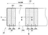
- FIG. 3 is a sectional view taken along line III-III in FIG. 2.
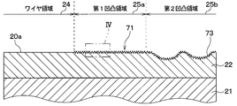
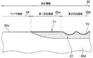
- FIG. 4 is an enlarged view of a region IV in FIG. 3. It is the top view seen from the arrow V direction in FIG. It is the top view seen from the arrow VI direction in FIG. It is a figure for demonstrating each area
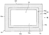
- the mold package 1 includes a mounting portion 10 and a plurality of terminal portions 20 arranged around the mounting portion 10. In FIG. 1, only one terminal portion 20 of the plurality of terminal portions 20 is illustrated.
- the mounting portion 10 and the terminal portion 20 are provided with a lead frame (not shown) in which the mounting portion 10 and the terminal portion 20 are integrated with a tie bar, an outer peripheral frame, etc., and the tie bar, the outer peripheral frame, etc. are appropriately removed. It is composed by being separated. That is, the mounting portion 10 and the terminal portion 20 are configured using a common lead frame.
- the mounting unit 10 includes a main metal part 11 made of a metal material and a metal thin film 12 formed so as to cover the main metal part 11.
- the terminal portion 20 includes a main metal portion 21 made of a metal material and a metal thin film 22 formed so as to cover the main metal portion 21.
- the main metal parts 11 and 21 are made of a metal material such as Cu (copper), Al (aluminum), Al alloy, Fe (iron), or Fe alloy.
- the metal thin films 12 and 22 are plating films, and are made of, for example, a metal material such as Ni (nickel), Pd (palladium), Ag (silver), or Au (gold). In the present embodiment, the metal thin films 12 and 22 are made of a Ni plating film.
- the mounting portion 10 has a plate shape, and has one surface 10a, the other surface 10b opposite to the one surface 10a, and four side surfaces 10c to 10f that connect the one surface 10a and the other surface 10b.
- side surfaces 10c and 10e among the side surfaces 10c to 10f are shown.
- the side surfaces 10d and 10f are side surfaces that connect the side surface 10c and the side surface 10e, respectively, as shown in FIG.
- the mounting portion 10 is configured such that the main metal portion 11 is covered with the metal thin film 12. For this reason, each surface 10a to 10f of the mounting portion 10 is constituted by a surface of the metal thin film 12 opposite to the main metal portion 11 side.
- the semiconductor chip 40 is mounted on the one surface 10 a of the mounting portion 10 via the bonding member 30.
- the semiconductor chip 40 for example, a silicon substrate on which a diode element or a MOSFET (that is, a Metal-Oxide-Semiconductor-Field-Effect-Transistor) element is formed is used.
- a diode element or a MOSFET that is, a Metal-Oxide-Semiconductor-Field-Effect-Transistor
- the joining member 30 for example, Ag paste, solder, or the like is used.
- the terminal portion 20 has a plate shape, and has one surface 20a, the other surface 20b opposite to the one surface 20a, and four side surfaces 20c to 20f connecting the one surface 20a and the other surface 20b.
- the plurality of terminal portions 20 are arranged around the mounting portion 10 so that the one surface 20a is substantially parallel to the one surface 10a of the mounting portion 10.
- a front side surface 20c on the mounting portion 10 side and a rear side surface 20e opposite to the mounting portion 10 side are shown.
- the side surfaces 20d and 20f are lateral side surfaces 20d and 20f that connect the front side surface 20c and the rear side surface 20e, respectively, as shown in FIG. 2 described later.
- the terminal portion 20 is configured such that the main metal portion 21 is covered with the metal thin film 22. For this reason, each surface 20a to 20f of the terminal portion 20 is constituted by a surface of the metal thin film 22 opposite to the main metal portion 21 side.
- the terminal portion 20 is electrically connected to the semiconductor chip 40 via the bonding wire 50 on the mounting portion 10 side on the one surface 20a.
- the bonding wire 50 is composed of, for example, an Al wire, an Au wire, or a Cu wire. In the present embodiment, the bonding wire 50 corresponds to a connection member.
- the mold resin 60 is arranged.
- the mold resin 60 is made of an epoxy resin. 1 shows the surface 10b of the mounting portion 10 exposed from the mold resin 60, but the surface 10b of the mounting portion 10 may also be sealed with the mold resin 60.
- the mounting portion 10 and the terminal portion 20 are configured to have a concavo-convex region having a concavo-convex shape in the sealing region sealed with the mold resin 60.
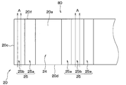
- the uneven area of the terminal portion 20 will be described with reference to FIGS.
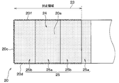
- the region sealed with the mold resin 60 in the terminal portion 20 will be described as the sealing region 23.
- the terminal unit 20 has a region on the mounting unit 10 side as a sealing region 23.
- the terminal part 20 has the wire area
- the terminal part 20 has the one surface uneven
- the wire region 24 corresponds to a connection region.
- the terminal portion 20 has a plate shape whose longitudinal direction is a direction from the front side surface 20c side to the rear side surface 20e side.
- the horizontal direction on the paper corresponds to the longitudinal direction.
- region 25 the wire area
- each one-side uneven region 25 the wire region 24 side is a first uneven region 25a, and the opposite side of the wire region 24 is the second uneven region 25b across the first uneven region 25a.
- the one-side uneven region 25 located on the opposite side to the front side surface 20c side of the two one-side uneven regions 25 has the first uneven region 25a on the opposite side to the wire region 24 side with the second uneven region 25b interposed therebetween.
- the sealing region 23 in the one surface 20a extends from the front side surface 20c side to the second uneven region 25b in the one surface uneven region 25 located on the opposite side of the front side surface 20c side.
- the first uneven region 25 a farthest from the front side surface 20 c is located outside the sealing region 23.
- region 23 may include all the one surface uneven
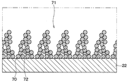
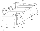
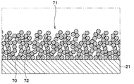
- the first uneven region 25 a has an uneven shape having a minute uneven portion 71 configured by laminating a plurality of metal particles 70 on the metal thin film 22.
- the fine uneven portion 71 has a plurality of metal particles 70 that taper from the metal thin film 22 side toward the opposite side of the metal thin film 22. It is comprised by laminating
- the gap 72 is configured in a state where the spaces between the adjacent metal particles 70 are connected to each other, and is connected to a space outside the region where the metal particles 70 are stacked.
- the metal particles 70 are stacked in a convex shape, it can be said that the void 72 is connected to a concave portion formed between adjacent convex portions, for example.
- the gap 72 has a cross-sectional size in the direction orthogonal to the one surface 20a of about several nm to 100 nm.
- the mold resin 60 is made of an epoxy resin, and the distance between molecular ends in a molten state is about 3 to 10 nm.
- the metal particles 70 are laminated so that a void 72 into which the molten resin constituting the mold resin 60 can enter is formed.
- the mold resin 60 enters the gap 72.
- the maximum unevenness 71 has a maximum height of 300 nm or less. In other words, the maximum length between the portion farthest from the metal thin film 22 and the metal thin film 22 is set to 300 nm or less.
- the metal particle 70 is made of an oxide made of the same material as that of the metal thin film 22. That is, in this embodiment, since the plating film is made of Ni, the fine uneven portion 71 is formed by stacking the metal particles 70 made of an oxide of Ni.
- the second uneven region 25 b As shown in FIG. 3, in the second uneven region 25 b, a plurality of groove portions 73 of about several ⁇ m are formed in the metal thin film 22, and the minute uneven portions 71 are formed on the metal thin film 22 including the groove portions 73. It is made the uneven shape. That is, the second uneven region 25b is formed with a groove 73 that is not formed in the first uneven region 25a, and has an uneven shape having a height difference larger than that of the first uneven region 25a.
- the above is the configuration of the one surface 20a of the terminal portion 20.
- gap 72 is formed in the micro uneven
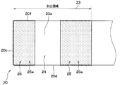
- the entire front surface 20 c of the terminal portion 20 is a sealing region 23.
- the front side surface 20 c has a region on the one surface 20 a side as a front side uneven region 26. That is, the front side surface 20 c has a front side uneven region 26 that is continuous with the second uneven region 25 b.
- the length of the front side uneven region 26 between the lateral side surface 20d and the lateral side surface 20f is substantially equal to the portion farthest from the one surface 20a.
- the front side uneven region 26 has the same configuration as that of the first uneven region 25a, and has an uneven shape formed by stacking a plurality of metal particles 70.
- the side surfaces 20 d and 20 f of the terminal portion 20 have a region on the mounting portion 10 side as a sealing region 23.
- the lateral side surface 20 d has a lateral side uneven region 27 on the one surface 20 a side in the sealing region 23.
- the lateral side uneven region 27 is configured as a region continuous with the first uneven region 25a and the second uneven region 25b in the region on the one surface 20a side of the lateral side surface 20d.
- region 27 has the short length from the area
- the lateral side surface uneven region 27 has the same configuration as the first uneven region 25a, and has an uneven shape formed by laminating a plurality of metal particles 70.
- the region connected to the first uneven region 25a in the lateral side surface 20d is, in other words, the region located immediately below the first uneven region 25a in the lateral side surface 20d.
- the region connected to the second uneven region 25b in the side surface 20d is, in other words, the region located immediately below the second uneven region 25b in the side surface 20d.
- the lateral side surface 20f has a lateral side uneven region 27 on the one surface 20a side in the same manner as the lateral side surface 20d.
- the above is the configuration of the terminal portion 20 in the present embodiment.
- a plurality of points indicating uneven shapes are shown in the one-surface uneven region 25 in FIG. 2, the front-side uneven region 26 in FIG. 5, and the lateral-side uneven region 27 in FIG. It is.
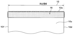
- the configuration of the mounting unit 10 will be described. In the following, a region sealed with the mold resin 60 in the mounting portion 10 will be described as a sealing region 13.
- the surface 10 a of the mounting portion 10 has a substantially central portion as a mounting region 14, and a region surrounding the mounting region 14 as a one-sided uneven region 15 having an uneven shape.
- the mounting region 14 is a region where the semiconductor chip 40 is disposed via the bonding member 30. Then, on the one surface 10 a of the mounting portion 10, as shown in FIG. 1, the one-surface uneven region 15 becomes a sealing region 13 that is sealed with the mold resin 60.
- the one-side uneven region 15 has a first uneven region 15a on the mounting region 14 side, and a second uneven region 15b on the opposite side of the first uneven region 15a. Similar to the first uneven region 25 a of the terminal portion 20, the first uneven region 15 a has an uneven shape in which a plurality of metal particles 70 are stacked to form a fine uneven portion 71. Further, in the second uneven region 15b, a plurality of groove portions 73 are formed as in the case of the second uneven region 25b of the terminal portion 20, and the minute uneven portion 71 is formed on the metal thin film 12 including the groove portion 73. The shape is uneven.
- the entire side surfaces 10c to 10f of the mounting portion 10 are sealed regions 13 respectively.
- region of the one surface 20a side is made into the side uneven
- the side uneven region 16 has an uneven shape in which a plurality of metal particles 70 are stacked to form a minute uneven portion 71.
- the length of the side uneven region 16 is substantially equal between the side surface 10d and the side surface 10f to the portion farthest from the one surface 10a.
- the region on the one surface 10a side is the side surface uneven region 16 as in the side surface 10c.
- a lead frame 80 in which the mounting portion 10 and the terminal portion 20 are integrated with a tie bar, an outer peripheral frame, or the like is prepared. 9 and 10, only one terminal portion 20 in the lead frame 80 is illustrated. In the present embodiment, the lead frame 80 corresponds to a base member.
- the one-side uneven region 15 and the side uneven region 16 are formed on the mounting portion 10. Further, the one-side uneven region 25, the front side uneven region 26, and the lateral side uneven region 27 are formed in the terminal portion 20.
- region 27 in the terminal part 20 is demonstrated concretely. Note that the process of forming the one-surface uneven area 15 and the side uneven area 16 on the mounting portion 10 is the same as the process of forming the one-surface uneven area 25, the front side uneven area 26, and the lateral side uneven area 27 on the terminal portion 20. .
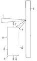
- a light source that oscillates the laser light L, a condenser lens, and the like are disposed as appropriate, and the region that becomes the second uneven region 25 b of the terminal portion 20 is irradiated with the laser light L.
- the laser is applied to a plurality of locations along the direction orthogonal to the longitudinal direction of the terminal portion 20. Irradiate light L.
- the light source is moved relative to the second uneven region 25b, and laser light is emitted to a plurality of positions along the arrow A.
- L is irradiated.
- the laser beam L may be irradiated using a so-called galvano scanner that arranges a mirror on the light source side and scans the laser beam L by rotating the mirror.
- the metal particles 70 float and a groove 73 having a size of about several ⁇ m is formed.
- the floating metal particles 70 are deposited around the area irradiated with the laser beam L.
- the floating metal particles 70 are stacked to form the minute uneven portion 71.
- the floating metal particles 70 are also deposited in a region around the region irradiated with the laser beam L. For this reason, on the one surface 20a, a plurality of metal particles 70 are laminated at a position adjacent to the second uneven region 25b to form the first uneven region 25a.
- a plurality of metal particles 70 are laminated on the one surface 20a side adjacent to the second uneven region 25b, and the front side uneven region 26 and the lateral surface uneven region 27 are configured. Is done. In this way, by forming the concavo-convex shape on the front side surface 20c and the lateral side surfaces 20d, 20f, it is not necessary to perform special processing on the side surfaces 20c, 20d, 20f, and the manufacturing process can be simplified. .
- the metal particles 70 are stacked so that the voids 72 are formed as described above. Further, on the lateral side surfaces 20d and 20f, the metal particles 70 are less likely to adhere as the distance from the second uneven region 25b increases. For this reason, as shown in FIG. 6, the length of the lateral side surface uneven region 27 to the portion farthest from the one surface 20a becomes shorter as the distance from the second uneven region 25b increases.
- the metal thin film 22 is formed of a Ni plating film as in this embodiment, the energy density is 300 J / cm 2 or less, the pulse width is 1 ⁇ m second or less, and the surface temperature of the metal thin film 22 is 1500. What is necessary is just to irradiate the laser beam L so that it may become about degreeC.
- the metal thin film 22 is comprised by Ni plating film
- the metal particle 70 when the laser beam L is irradiated on the said conditions, the metal particle 70 will be the said from the metal thin film 22 side, as FIG. 4 shows. It vapor-deposits so that it may become a taper shape toward the metal thin film 22 and an other side.
- the clear principle is not clear about this, when the floating metal particle 70 vapor-deposits, it is estimated that it is difficult to rearrange because the metal particle 70 has a small energy.
- the one-side uneven region 25, the front side uneven region 26, and the lateral side uneven region 27 are formed in the terminal portion 20.
- the laser beam L is irradiated to the second uneven region 15b also in the mounting portion 10.
- the second uneven region 15b is formed with the groove 73 and the metal particles 70 are laminated to form an uneven shape.
- region 15a is comprised by the circumference
- the side surface uneven region 16 is configured by laminating metal particles 70 in a region on the one surface 10a side adjacent to the second uneven region 15b.
- the semiconductor chip 40 is mounted on the mounting region 14 of the mounting unit 10 via the bonding member 30. And wire bonding is performed and the semiconductor chip 40 and the terminal part 20 are joined. Note that wire bonding is performed on the wire region 24 in the terminal portion 20.
- the product subjected to the above steps is placed in a mold (not shown), and a molten resin constituting the mold resin 60 is poured into the mold and solidified. At this time, the molten resin is solidified in such a state that the gap 72 is large enough to enter the molten resin. Thereafter, the mold package is configured by appropriately removing the outer peripheral frame and the like.
- the mounting unit 10 has the one surface uneven area 15 on the one surface 10a and the side surface uneven areas 16 on the side surfaces 10c to 10f. Therefore, it is possible to suppress the mold resin 60 from being peeled from the side surfaces 10c to 10f of the mounting portion 10.
- the terminal portion 20 includes a single-sided uneven region 25 on one surface 20a, and side-surface uneven regions 26 and 27 on the side surfaces 20c, 20d, and 20f. For this reason, it can suppress that the mold resin 60 peels from the side surfaces 20c, 20d, and 20f of the terminal part 20.
- a gap 72 is formed between the adjacent metal particles 70.
- the mold resin 60 is also in a state where it enters the gap 72. For this reason, compared with the case where the space
- the wire region 24 of the terminal portion 20 is also configured to have a concavo-convex shape with respect to the first embodiment, and the other aspects are the same as those in the first embodiment. Omitted.
- the terminal portion 20 is in a state where the wire region 24 is a first uneven region 25 a and the wire region 24 is sandwiched between two second uneven regions 25 b. Yes.
- the one surface 20 a of the terminal portion 20 is a single surface uneven region 25 in the sealing region 23.
- corrugated shape is shown.
- the periphery of the region to which the bonding wire 50 is actually connected is also made uneven. For this reason, the adhesion between the wire region 24 and the mold resin 60 can be improved.
- wire bonding when wire bonding is performed on the wire region 24, for example, it is performed by applying ultrasonic vibration in a state where the wire is pressed against the wire region 24.
- the present inventors have found that when the height difference of the unevenness is 300 nm or less, the bondability at the time of performing wire bonding does not deteriorate. And the 1st uneven
- the metal particles 70 suspended from the second uneven region 25 b may be deposited on the wire region 24.
- the metal particles 70 may be suspended from the second uneven region 25 b so that the metal particles 70 are deposited on the wire region 24.
- the second uneven region 25 b is located adjacent to the wire region 24.
- the lateral side surface 20d, 20f is also formed with the lateral side uneven region 27 in a portion connected to the wire region 24 in the region on the one surface 20a side.
- a region different from the wire region 24 in the sealing region 23 of the one surface 20 a is a first uneven region 25 a, and the second uneven region 25b is not formed.
- the front side surface 20 c has the entire region as a front side uneven region 26.
- the lateral side surfaces 20 d and 20 f are all lateral side uneven regions 27 that become the sealing region 23.
- the mounting portion 10 includes a first uneven region 15a in which the entire region different from the mounting region 14 is formed in the sealing region 23 of the one surface 10a, and the second uneven region 25b is formed. Absent. Although not particularly illustrated, the entire side surfaces 10c to 10f are the side surface uneven regions 16.
- a lead frame 80 in which the mounting portion 10 and the terminal portion 20 are integrated with a tie bar, an outer peripheral frame, or the like is prepared. Then, a mask (not shown) is arranged on the wire region 24 in the mounting unit 10. Next, the target member 90 is disposed in the vicinity of the region of the terminal portion 20 where the metal particles 70 are to be laminated.
- the target member 90 is made of Ni.
- the target member 90 is irradiated with the laser beam L, and the metal particles 70 are floated from the target member 90 and deposited on the terminal portion 20 to be laminated.
- the metal particle 70 is laminated
- region 25a is comprised.
- the mask formed in the wire region 24 is removed.
- the one surface 20 a of the terminal portion 20 has a configuration in which the first uneven region 25 a is formed in a region different from the wire region 24.
- a front side uneven region 26 and a lateral side uneven region 27 are formed, respectively.
- the metal particles 70 can be stacked at desired locations on the side surfaces 20c, 20d, and 20f by moving the target member 90 or the like. In other words, in the present embodiment, by moving the target member 90 or the like, the metal particles 70 are stacked on all the regions of the side surfaces 20c, 20d, and 20f to form an uneven shape.
- the metal particles 70 are 0.25 mm from the target member 90. Float to a certain height. For this reason, the metal particle 70 can be vapor-deposited on the terminal part 20 from the target member 90, and can be laminated
- the energy density or the like of the laser light L applied to the target member 90 is increased, the floating distance of the metal particles 70 floating from the target member 90 becomes longer. For this reason, if the metal particles 70 are vapor-deposited from the target member 90 to the terminal portion 20, the energy density of the laser light L and the interval between the target member 90 and the terminal portion 20 can be changed as appropriate. However, as described above, if the energy density of the laser light L is excessively increased, metal particles may be scattered from the target member 90. Therefore, the energy density of the laser light L should be 300 J / cm 2 or less. Is preferred.
- the metal particles 70 are suspended from the target member 90 and vapor-deposited on the mounting portion 10 even in the mounting portion 10.
- the mounting part 10 can be set as the structure by which the metal particle 70 is not vapor-deposited in the mounting area
- the uneven shape can be formed at a desired location.
- an uneven shape can be formed on the other surface 20b side of the side surfaces 20c, 20d, and 20f of the terminal portion 20. Therefore, the adhesion with the mold resin 60 can be further improved.
- the terminal portion 20 is an example in which the entire region of the front side surface 20 c is the front side uneven region 26 and the entire region that becomes the sealing region 23 of the side surfaces 20 d and 20 f is the side surface uneven region 27.
- the terminal portion 20 for example, only one surface 20a side of the front side surface 20c is the front side uneven region 26, and only one surface 20a side that becomes the sealing region 23 of the side surfaces 20d and 20f is the side surface uneven region 27. It may be. That is, in this embodiment, since the metal particles 70 are suspended from the target member 90 to form the uneven shape, the uneven shape can be formed at a desired location, and the range in which the uneven shape is configured can be changed as appropriate.
- a mask may not be formed in the wire region 24 of the terminal portion 20, and the wire region 24 may also be a first uneven region 25a as shown in FIG. That is, as for the terminal part 20, the whole area
- the first uneven region 25a is configured by the minute uneven portion 71 having a maximum height of 300 nm or less, so that the adhesion with the molding resin 60 is improved and the bonding wire 50 is connected. It is possible to suppress a decrease in bondability.
- the terminal portion 20 is composed of a main metal portion 21 composed of Al or an Al alloy, and the metal thin film 22 is not provided.
- region 25a is made into the uneven
- each surface 20 a to 20 f is composed of the main metal portion 21.
- the minute uneven portion 71 of the present embodiment is configured by laminating a plurality of metal particles 70, and the plurality of metal particles 70 are arranged in a substantially layer shape. That is, in the present embodiment, the plurality of metal particles 70 are regularly arranged from the metal particles 70 described with reference to FIG.
- grooved part 71 of this embodiment is comprised by the uneven
- the maximum unevenness 71 has a maximum height of 300 nm or less.
- a gap 72 is formed between adjacent metal particles 70.
- the gap 72 has a size that allows the molten resin constituting the mold resin 60 to enter, as in the first embodiment. Then, the mold resin 60 enters the gap 72.
- the second uneven region 25 b has an uneven shape in which the above-described substantially layered minute uneven portion 71 is formed on the metal thin film 22 including the groove portion 73.
- region 27 are made into the uneven
- the mounting portion 10 is composed of a main metal portion 11 composed of Al or an Al alloy, and the metal thin film 12 is not provided.
- region 15a is set as the structure similar to the 1st uneven
- the second uneven region 15 b has an uneven shape in which the substantially layered minute uneven portion 71 is formed on the metal thin film 12 including the groove 73.
- the side uneven region 16 has an uneven shape in which the substantially layered minute uneven portion 71 is formed, like the first uneven region 25a.
- each surface 10a to 10f is composed of the main metal portion 11.
- Such an uneven shape is formed by irradiating the laser beam L under the same conditions as in the first embodiment.
- the clear principle is not clear also about this, it estimates as follows. That is, Al or Al alloy has a melting point lower than Ni. For this reason, when the main metal portions 11 and 21 are made of Al or an Al alloy so that the laser beam L is irradiated, the metal thin films 12 and 22 are made of an Ni plating film so that the laser beam L is irradiated.
- the floating metal particle 70 has a larger energy than the case of the above. Therefore, when the laser beam L is irradiated under the same conditions as in the first embodiment, when the floating metal particles 70 are deposited, the energy lost until the metal particles 70 are fixed increases. It is presumed that it becomes possible to arrange regularly after the deposition.
- the concavo-convex shape may be substantially layered by laminating the metal particles 70. Further, such a concavo-convex shape has a larger proportion of the voids 72 than the concavo-convex shape of the first embodiment, and an amount of entering the voids 72 of the mold resin 60 is increased. For this reason, the adhesiveness of the mounting part 10 and the terminal part 20, and the mold resin 60 can be improved further.
- the mold resin 60 may contain a filler such as alumina or silica for adjusting the linear expansion coefficient in the epoxy resin.
- the metal thin film 22 has laminated
- a material for forming the bonding wire 50 and a bonding plating film having high bonding properties may be laminated.
- the metal particles 70 are laminated on the bonding plating film to form an uneven shape.
- the target member 90 may be configured by using a metal material different from that of the metal thin film 22, and may be configured by, for example, Fe, Al, Sn (tin), or the like. Even if such a target member 90 is used, it is possible to form a concavo-convex shape by laminating metal particles 70 at desired locations of the mounting portion 10 and the terminal portion 20. That is, in the said 3rd Embodiment, what is comprised with the material different from the material which comprises the metal thin film 22 can be used as the target member 90, and the freedom degree of design can be improved.
- stack can be changed suitably according to a use application, and the freedom degree of design can be improved.
- the fourth embodiment is performed by irradiating the laser beam L under the same conditions as in the third embodiment.
- the plurality of metal particles 70 are arranged in a substantially layered manner and stacked.
- a flexible substrate made of a resin may be used as a base material, and metal particles 70 may be laminated on a desired region of the flexible substrate to form an uneven shape.
- the groove 73 is formed and the metal particles 70 are floated, and the floating metal particles 70 are deposited and stacked. May be irradiated.
- the principle of sputtering may be applied to cause metal particles to collide.
- metal particles may collide with the target member 90 to float the metal particles 70 from the target member 90.
Landscapes
- Structures Or Materials For Encapsulating Or Coating Semiconductor Devices Or Solid State Devices (AREA)
- Encapsulation Of And Coatings For Semiconductor Or Solid State Devices (AREA)
- Lead Frames For Integrated Circuits (AREA)
- Engineering & Computer Science (AREA)
- Microelectronics & Electronic Packaging (AREA)
Priority Applications (3)
| Application Number | Priority Date | Filing Date | Title |
|---|---|---|---|
| CN201880024454.9A CN110520979B (zh) | 2017-04-14 | 2018-03-08 | 基材、利用该基材的模塑封装、基材的制造方法以及模塑封装的制造方法 |
| DE112018001998.5T DE112018001998B4 (de) | 2017-04-14 | 2018-03-08 | Basismaterial, formpackung, die dasselbe verwendet, basismaterialherstellungsverfahren und formpackungsherstellungsverfahren |
| US16/596,897 US11114368B2 (en) | 2017-04-14 | 2019-10-09 | Base material, mold package, base material manufacturing method, and mold package manufacturing method |
Applications Claiming Priority (2)
| Application Number | Priority Date | Filing Date | Title |
|---|---|---|---|
| JP2017080679A JP6724851B2 (ja) | 2017-04-14 | 2017-04-14 | 基材、それを用いたモールドパーケージ、基材の製造方法、およびモールドパッケージの製造方法 |
| JP2017-080679 | 2017-04-14 |
Related Child Applications (1)
| Application Number | Title | Priority Date | Filing Date |
|---|---|---|---|
| US16/596,897 Continuation US11114368B2 (en) | 2017-04-14 | 2019-10-09 | Base material, mold package, base material manufacturing method, and mold package manufacturing method |
Publications (1)
| Publication Number | Publication Date |
|---|---|
| WO2018190046A1 true WO2018190046A1 (ja) | 2018-10-18 |
Family
ID=63792333
Family Applications (1)
| Application Number | Title | Priority Date | Filing Date |
|---|---|---|---|
| PCT/JP2018/009056 Ceased WO2018190046A1 (ja) | 2017-04-14 | 2018-03-08 | 基材、それを用いたモールドパーケージ、基材の製造方法、およびモールドパッケージの製造方法 |
Country Status (5)
| Country | Link |
|---|---|
| US (1) | US11114368B2 (enExample) |
| JP (1) | JP6724851B2 (enExample) |
| CN (1) | CN110520979B (enExample) |
| DE (1) | DE112018001998B4 (enExample) |
| WO (1) | WO2018190046A1 (enExample) |
Cited By (2)
| Publication number | Priority date | Publication date | Assignee | Title |
|---|---|---|---|---|
| JP2021088092A (ja) * | 2019-12-03 | 2021-06-10 | いすゞ自動車株式会社 | 樹脂組成物との接合用の金属部材、金属樹脂接合体の製造方法、および金属樹脂接合体 |
| US20220068790A1 (en) * | 2018-03-26 | 2022-03-03 | Texas Instruments Incorporated | Electronic Device Having Inverted Lead Pins |
Families Citing this family (6)
| Publication number | Priority date | Publication date | Assignee | Title |
|---|---|---|---|---|
| JP6777063B2 (ja) | 2017-12-20 | 2020-10-28 | 株式会社デンソー | 電子装置およびその製造方法 |
| JP6784342B2 (ja) * | 2018-05-01 | 2020-11-11 | 株式会社村田製作所 | 電子デバイスおよびそれを搭載した指紋認証装置 |
| US12476169B2 (en) | 2020-03-11 | 2025-11-18 | Rohm Co., Ltd. | Semiconductor device |
| US11784050B2 (en) | 2021-04-27 | 2023-10-10 | Micron Technology, Inc. | Method of fabricating microelectronic devices and related microelectronic devices, tools, and apparatus |
| JP2023007028A (ja) * | 2021-07-01 | 2023-01-18 | ローム株式会社 | 半導体装置 |
| DE102023106492A1 (de) * | 2023-03-15 | 2024-09-19 | Ams-Osram International Gmbh | Leiterrahmen, bauteil mit einem leiterrahmen und verfahren zur herstellung eines leiterrahmens |
Citations (3)
| Publication number | Priority date | Publication date | Assignee | Title |
|---|---|---|---|---|
| JP2002280512A (ja) * | 2001-03-19 | 2002-09-27 | Denso Corp | リードフレームの製造方法 |
| JP2012243889A (ja) * | 2011-05-18 | 2012-12-10 | Denso Corp | 半導体装置およびその製造方法 |
| JP2016105432A (ja) * | 2014-12-01 | 2016-06-09 | Shマテリアル株式会社 | リードフレームの製造方法 |
Family Cites Families (13)
| Publication number | Priority date | Publication date | Assignee | Title |
|---|---|---|---|---|
| JPH0832006A (ja) | 1994-07-18 | 1996-02-02 | Daido Steel Co Ltd | Icパッケージ用リードフレーム材 |
| JP4641605B2 (ja) | 2000-09-27 | 2011-03-02 | イビデン株式会社 | 接着剤、セラミック構造体及びその製造方法 |
| JP4595505B2 (ja) | 2004-11-24 | 2010-12-08 | ソニー株式会社 | モールド及びその製造方法、パターンの形成方法 |
| KR100819800B1 (ko) | 2005-04-15 | 2008-04-07 | 삼성테크윈 주식회사 | 반도체 패키지용 리드 프레임 |
| JP4609172B2 (ja) | 2005-04-21 | 2011-01-12 | 株式会社デンソー | 樹脂封止型半導体装置 |
| JP2007258205A (ja) | 2006-03-20 | 2007-10-04 | Denso Corp | 電子装置およびその製造方法 |
| US20080001264A1 (en) * | 2006-07-03 | 2008-01-03 | Texas Instruments Incorporated | Exposed top side copper leadframe manufacturing |
| JP2014093425A (ja) | 2012-11-02 | 2014-05-19 | Sumitomo Metal Mining Co Ltd | Znを主成分とするはんだ合金との接合部を有する電子部品 |
| JP5983700B2 (ja) | 2013-12-09 | 2016-09-06 | 株式会社デンソー | 半導体装置およびその製造方法、複合成形体 |
| JP6578900B2 (ja) | 2014-12-10 | 2019-09-25 | 株式会社デンソー | 半導体装置及びその製造方法 |
| JP6459656B2 (ja) | 2015-03-10 | 2019-01-30 | 株式会社村田製作所 | 接合用部材およびそれを用いた電子部品の実装方法 |
| JP6618328B2 (ja) | 2015-10-28 | 2019-12-11 | 東亜建設工業株式会社 | 泥土の脱水処理方法 |
| US10211131B1 (en) * | 2017-10-06 | 2019-02-19 | Microchip Technology Incorporated | Systems and methods for improved adhesion between a leadframe and molding compound in a semiconductor device |
-
2017
- 2017-04-14 JP JP2017080679A patent/JP6724851B2/ja active Active
-
2018
- 2018-03-08 DE DE112018001998.5T patent/DE112018001998B4/de active Active
- 2018-03-08 CN CN201880024454.9A patent/CN110520979B/zh active Active
- 2018-03-08 WO PCT/JP2018/009056 patent/WO2018190046A1/ja not_active Ceased
-
2019
- 2019-10-09 US US16/596,897 patent/US11114368B2/en active Active
Patent Citations (3)
| Publication number | Priority date | Publication date | Assignee | Title |
|---|---|---|---|---|
| JP2002280512A (ja) * | 2001-03-19 | 2002-09-27 | Denso Corp | リードフレームの製造方法 |
| JP2012243889A (ja) * | 2011-05-18 | 2012-12-10 | Denso Corp | 半導体装置およびその製造方法 |
| JP2016105432A (ja) * | 2014-12-01 | 2016-06-09 | Shマテリアル株式会社 | リードフレームの製造方法 |
Cited By (4)
| Publication number | Priority date | Publication date | Assignee | Title |
|---|---|---|---|---|
| US20220068790A1 (en) * | 2018-03-26 | 2022-03-03 | Texas Instruments Incorporated | Electronic Device Having Inverted Lead Pins |
| US11699649B2 (en) * | 2018-03-26 | 2023-07-11 | Texas Instruments Incorporated | Electronic device having inverted lead pins |
| JP2021088092A (ja) * | 2019-12-03 | 2021-06-10 | いすゞ自動車株式会社 | 樹脂組成物との接合用の金属部材、金属樹脂接合体の製造方法、および金属樹脂接合体 |
| JP7255466B2 (ja) | 2019-12-03 | 2023-04-11 | いすゞ自動車株式会社 | 樹脂組成物との接合用の金属部材、金属樹脂接合体の製造方法、および金属樹脂接合体 |
Also Published As
| Publication number | Publication date |
|---|---|
| CN110520979B (zh) | 2023-11-10 |
| DE112018001998B4 (de) | 2022-02-03 |
| DE112018001998T5 (de) | 2019-12-24 |
| CN110520979A (zh) | 2019-11-29 |
| US11114368B2 (en) | 2021-09-07 |
| JP6724851B2 (ja) | 2020-07-15 |
| JP2018182101A (ja) | 2018-11-15 |
| US20200043835A1 (en) | 2020-02-06 |
Similar Documents
| Publication | Publication Date | Title |
|---|---|---|
| WO2018190046A1 (ja) | 基材、それを用いたモールドパーケージ、基材の製造方法、およびモールドパッケージの製造方法 | |
| CN109891575B (zh) | 电子装置及其制造方法 | |
| US10264677B2 (en) | Electronic component and manufacturing method therefor | |
| JP5565315B2 (ja) | 半導体装置の製造方法 | |
| TW538663B (en) | Multilayer wiring board and method of fabrication thereof | |
| JP6776801B2 (ja) | 電子装置及びその製造方法 | |
| CN1771767A (zh) | 制造电子模块的方法以及电子模块 | |
| JP2011512260A (ja) | Mems部品、mems部品の製造方法、及びmems部品の取り扱い方法 | |
| JP7037368B2 (ja) | 半導体装置および半導体装置の製造方法 | |
| JP2014154848A (ja) | 樹脂封止型半導体装置の製造方法およびリードフレーム | |
| JP2017028228A (ja) | マルチチップモジュールおよびその製造方法 | |
| US11517982B2 (en) | Electronic device and method for manufacturing the same | |
| WO2013054898A1 (ja) | チップ抵抗器、チップ抵抗器の実装構造、およびチップ抵抗器の製造方法 | |
| JP2011054889A (ja) | 樹脂封止型半導体装置およびその製造方法 | |
| US8623450B2 (en) | Method for producing a flexible circuit configuration | |
| CN111261647B (zh) | 一种透光盖板、光学传感器及其制造方法 | |
| JP6776800B2 (ja) | 電子装置及びその製造方法 | |
| US20220361333A1 (en) | Electronic element mounting substrate, electronic device, and electronic module | |
| CN204696104U (zh) | 一种系统级mems双载体芯片封装件 | |
| US11382218B2 (en) | Printed wiring board and method for manufacturing the same | |
| CN115064477A (zh) | 供体基板、转移设备与供体基板制备方法 | |
| TW200529383A (en) | Electrode package for semiconductor device | |
| JPS63304655A (ja) | 積層体の製造方法 | |
| CN111696928B (zh) | 半导体封装结构及其制造方法 | |
| EP4113590A1 (en) | Electronic component mounting package and electronic device |
Legal Events
| Date | Code | Title | Description |
|---|---|---|---|
| 121 | Ep: the epo has been informed by wipo that ep was designated in this application |
Ref document number: 18785131 Country of ref document: EP Kind code of ref document: A1 |
|
| 122 | Ep: pct application non-entry in european phase |
Ref document number: 18785131 Country of ref document: EP Kind code of ref document: A1 |