WO2018174019A1 - In-Cu焼結体スパッタリングターゲット及びIn-Cu焼結体スパッタリングターゲットの製造方法 - Google Patents
In-Cu焼結体スパッタリングターゲット及びIn-Cu焼結体スパッタリングターゲットの製造方法 Download PDFInfo
- Publication number
- WO2018174019A1 WO2018174019A1 PCT/JP2018/010847 JP2018010847W WO2018174019A1 WO 2018174019 A1 WO2018174019 A1 WO 2018174019A1 JP 2018010847 W JP2018010847 W JP 2018010847W WO 2018174019 A1 WO2018174019 A1 WO 2018174019A1
- Authority
- WO
- WIPO (PCT)
- Prior art keywords
- compound
- phase
- sputtering target
- sintered
- less
- Prior art date
- Legal status (The legal status is an assumption and is not a legal conclusion. Google has not performed a legal analysis and makes no representation as to the accuracy of the status listed.)
- Ceased
Links
Images

Classifications
-
- Y—GENERAL TAGGING OF NEW TECHNOLOGICAL DEVELOPMENTS; GENERAL TAGGING OF CROSS-SECTIONAL TECHNOLOGIES SPANNING OVER SEVERAL SECTIONS OF THE IPC; TECHNICAL SUBJECTS COVERED BY FORMER USPC CROSS-REFERENCE ART COLLECTIONS [XRACs] AND DIGESTS
- Y02—TECHNOLOGIES OR APPLICATIONS FOR MITIGATION OR ADAPTATION AGAINST CLIMATE CHANGE
- Y02E—REDUCTION OF GREENHOUSE GAS [GHG] EMISSIONS, RELATED TO ENERGY GENERATION, TRANSMISSION OR DISTRIBUTION
- Y02E10/00—Energy generation through renewable energy sources
- Y02E10/50—Photovoltaic [PV] energy
- Y02E10/541—CuInSe2 material PV cells
-
- Y—GENERAL TAGGING OF NEW TECHNOLOGICAL DEVELOPMENTS; GENERAL TAGGING OF CROSS-SECTIONAL TECHNOLOGIES SPANNING OVER SEVERAL SECTIONS OF THE IPC; TECHNICAL SUBJECTS COVERED BY FORMER USPC CROSS-REFERENCE ART COLLECTIONS [XRACs] AND DIGESTS
- Y02—TECHNOLOGIES OR APPLICATIONS FOR MITIGATION OR ADAPTATION AGAINST CLIMATE CHANGE
- Y02P—CLIMATE CHANGE MITIGATION TECHNOLOGIES IN THE PRODUCTION OR PROCESSING OF GOODS
- Y02P70/00—Climate change mitigation technologies in the production process for final industrial or consumer products
- Y02P70/50—Manufacturing or production processes characterised by the final manufactured product
Definitions
- the present invention relates to an In—Cu sintered sputtering target used for forming a thin film of In—Cu alloy, and a method of manufacturing the In—Cu sintered sputtering target.
- This application claims priority to Japanese Patent Application No. 2017-057334 filed in Japan on March 23, 2017 and Japanese Patent Application No. 2018-024509 filed in Japan on February 14, 2018. This is incorporated here.
- CIGS solar cells including a light absorption layer made of a Cu—In—Ga—Se alloy thin film have been widely provided as thin film solar cells made of a compound semiconductor.
- a method of forming a light absorption layer made of a Cu—In—Ga—Se alloy thin film a method of forming a film by vapor deposition is known.
- the solar cell provided with the light absorption layer formed by the vapor deposition method has an advantage that the energy exchange efficiency is high, there is a problem that the film formation rate is low and the production efficiency is low.
- a method of forming a light absorption layer made of a Cu—In—Ga—Se alloy thin film a thin film containing In, Cu and Ga or a thin film containing these elements is formed, and the thin film or the laminated film is formed.
- a method of heat-treating selenium in a Se atmosphere When forming a thin film containing In, Cu, and Ga or a laminated film of thin films containing these elements, a sputtering method using a sputtering target containing each element is applied.
- Patent Document 1 proposes an indium target containing 0.5 to 7.5 at% of Cu.
- Patent Document 1 discloses a casting method in which an indium alloy containing 0.5 to 7.5 at% Cu is melt-cast as a method for producing an indium target.
- Patent Document 2 proposes an In—Cu alloy sputtering target containing 30 to 80 atomic% of Cu.
- the In—Cu alloy film is formed by performing sputtering with a Cu chip chip-on a pure In target.
- Patent Document 3 discloses a method of forming a repaired target by cold isostatic pressing a powder having a first phase containing copper and indium on the surface of a sputtering target containing copper and indium. Yes.
- a powder containing copper, indium and gallium is used.
- Japanese Unexamined Patent Publication No. 2012-052190 A) Japanese Unexamined Patent Publication No. 2012-079997 (A) Japanese National Table 2014-503687 (A)
- the present invention has been made in view of the circumstances described above, and has an excellent workability and can suppress the occurrence of abnormal discharge during sputtering, and the In-Cu sputtering target. It aims at providing the manufacturing method of.
- an In—Cu sputtering target of one embodiment of the present invention is an In—Cu sintered sputtering target, and In In a range of 10 atomic% to 90 atomic%, with the balance being composed of Cu and inevitable impurities, a theoretical density ratio of 97% or more, and a variation in density within 2%. It is a feature.
- the n-Cu sintered sputtering target having the above-described structure contains relatively soft In at 10 atomic% or more, so that it is possible to suppress the occurrence of coarse chipping (chips) exceeding 1 mm and to result from chipping marks.
- the occurrence of abnormal discharge can be suppressed, and the density of the target is increased.
- the In content is 90 atomic% or less, the amount of processing waste generated by processing such as cutting is reduced, and the processing waste is less likely to adhere to the target surface. Therefore, the processability is excellent.
- the theoretical density ratio is as high as 97% or more, it is dense and has few vacancies, the occurrence of abnormal discharge and cracking during sputtering can be suppressed.
- the density variation is as low as 2% or less and the composition uniformity is high, the occurrence of abnormal discharge during sputtering can be further suppressed, and the film formation rate is stabilized.
- the Cu alloy thin film tends to have a uniform composition and film thickness.
- the variation in the In content is preferably within 3%.
- the variation in the In content is as small as 3% or less, the occurrence of abnormal discharge during sputtering is further suppressed, and the composition of the formed In—Cu alloy thin film is more likely to be uniform.
- an In single phase and a CuIn compound phase are present, and the In single phase preferably has a maximum particle diameter of 1 mm or less.
- the maximum particle diameter of the In single phase is relatively small, 1 mm or less, even when the sputter surface is consumed by sputtering, unevenness of the sputter surface is suppressed, and abnormal discharge during sputtering is generated. Can be suppressed.
- the In—Cu sintered sputtering target of the present invention further contains one or more of NaF, NaCl, Na 2 S, and Na 2 Se as the Na compound, and the maximum particle size of this Na compound is 15 ⁇ m or less. It is preferable that In this case, since the Na compound is contained, an In—Cu alloy thin film containing Na which is an alkali metal can be formed. In addition, since the maximum particle size of the Na compound is 15 ⁇ m or less, the occurrence of abnormal discharge during sputtering can be suppressed.
- the In—Cu sintered sputtering target of the present invention further contains one or more of KF, KCl, K2S, and K2Se as the K compound, and the maximum particle size of the K compound is 15 ⁇ m.
- KF KF
- KCl KCl
- K2S K2Se
- the maximum particle size of the K compound is 15 ⁇ m. The following is preferable.
- the K compound is contained, an In—Cu alloy thin film containing K which is an alkali metal can be formed.
- the maximum particle size of the K compound is 15 ⁇ m or less, the occurrence of abnormal discharge during sputtering can be suppressed.
- the method for producing an In—Cu sputtering target according to another aspect of the present invention (hereinafter referred to as “the method for producing an In—Cu sputtering target of the present invention”) is the above-described method for producing an In—Cu sintered sputtering target.
- the In powder of the In single phase is relatively uniform in the sintering process. Easy to diffuse into. When In diffuses throughout the raw material powder, it is possible to obtain a dense In—Cu sintered sputtering target with small variations in density.
- an In—Cu sintered sputtering target having excellent workability and capable of suppressing the occurrence of abnormal discharge during sputtering, and a method for producing the In—Cu sintered sputtering target. can do.
- the In—Cu sintered sputtering target according to the present embodiment contains In in a range of 10 atomic% to 90 atomic%, and the balance is composed of Cu and inevitable impurities.
- the variation of the In content is assumed to be within 3%.
- the theoretical density ratio (relative density with respect to the theoretical density calculated from the above composition ratio) is 97% or more, and the density variation is within 2%.
- FIG. 1 is an example of an element distribution diagram of an In—Cu sintered sputtering target according to an embodiment of the present invention.
- the white region in the left figure is a CuIn compound phase
- the black region in the left figure is an In single phase.
- the In single phase means a region where In is detected but Cu is not detected
- the CuIn compound phase means a region where In and Cu are detected.
- CuIn compounds constituting the CuIn compound phase are Cu7In3, Cu1In1, Cu11In9, and the like.
- the maximum particle size of the In single phase is 1 mm or less.
- the maximum particle diameter of the CuIn compound phase is 150 ⁇ m or less.
- the Na compound may further contain one or more of NaF, NaCl, Na2S, and Na2Se, and the maximum particle size of the Na compound may be 15 ⁇ m or less.
- the maximum particle size of the Na compound is preferably 10 ⁇ m or less, more preferably 5 ⁇ m or less.
- KF, KCl, K2S, and K2Se may be contained as the K compound, and the maximum particle size of the K compound may be 15 ⁇ m or less. From the viewpoint of suppressing abnormal discharge, the maximum particle size of the K compound is preferably 10 ⁇ m or less, more preferably 5 ⁇ m or less.
- the In content and its variation, the theoretical density ratio, the variation in density, the maximum particle size of the In single phase and the CuIn compound phase, Na compound and K The reason why the compound is defined as described above will be described.
- the In content is set within a range of 10 atomic% to 90 atomic%.
- the In content is preferably 20 atomic percent or more and 80 atomic percent or less.
- an In—Cu alloy thin film having a uniform film composition By reducing variation in the In content, an In—Cu alloy thin film having a uniform film composition can be formed. Here, if the variation in the In content exceeds 3%, the variation in the composition of the In—Cu alloy thin film to be formed may increase.
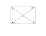
- the variation in the In content is measured as follows when the sputtering surface of the In—Cu sintered sputtering target is rectangular as shown in FIG. 2, for example. . (2), (3), (4), (5) located at the intersection (1) where the diagonal lines connecting the opposite corners of the sputtering surface intersect with each other and within 10% of the total length of the diagonal lines from the corners on each diagonal line ) Are cut into a square shape so that the length of one side is 5% of the length of the short side of the sputtering surface, and a cubic target piece is cut out. The cut-out cubic target pieces are divided into three equal parts in the thickness direction to obtain a total of 15 thin cubic target pieces.
- the In content is measured by the ICP-AES method.
- the average value of the measured In content is calculated, and the maximum value and the minimum value of the measured In content are extracted.
- the variation of the In content is a value obtained by the following formula.
- Variation of In content (%) ⁇ (maximum value of In content ⁇ minimum value of In content) / average value of In content ⁇ ⁇ 100
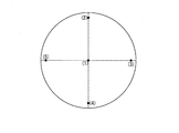
- a thin cubic target piece used as an analysis sample is produced as follows. (2), (3), (4) located at a position within 10% of the total length of the diagonal line from the center (1) of the sputter surface and the outer peripheral portions on two straight lines that pass through the center of the sputter surface and are orthogonal to each other ) And (5), the target is cut into a square shape so that the length of one side is 5% of the length of the diameter of the sputtering surface, and a cubic target piece is cut out. The cut-out cubic target pieces are divided into three equal parts in the thickness direction to obtain a total of 15 thin cubic target pieces.
- Theoretical density ratio 97% or more If the theoretical density ratio of the In—Cu sintered sputtering target is less than 97%, there are many vacancies, and abnormal discharge and cracking may occur easily during sputtering. Therefore, in this embodiment, the theoretical density ratio is defined to be 97% or more. The theoretical density ratio is usually 100% or less.
- the theoretical density is a value obtained by the following equation.
- Theoretical density ratio (%) (measured density / theoretical density) ⁇ 100
- the “measurement density” is measured using the Archimedes method. The theoretical density varies depending on the content ratio of In, Cu, and CuIn compounds. For this reason, in this embodiment, a molten metal having the same content ratio of In and Cu as that of the In—Cu sintered sputtering target is melted and cast and slowly cooled (cooling rate 5 ° C./min. The density of a defect-free ingot (10 cm ⁇ 10 cm ⁇ 10 cm) obtained by the following is measured, and the value is defined as “theoretical density”. It is visually confirmed whether or not it is a defect-free ingot.
- the theoretical density of an In—Cu sintered body sputtering target contains a Na compound or a K compound
- the theoretical density varies depending on the content of these.
- a theoretical density is calculated from each theoretical density and content of InCu, Na compound, and K compound.
- the theoretical density of an In—Cu sintered sputtering target containing NaF as a Na compound and KF as a K compound can be calculated by the following method. First, the theoretical density of InCu (InCu having a content ratio of In and Cu excluding Na compound and K compound) is measured by the above method, and the value is defined as Da (g / cm3).
- the theoretical density of NaF is 2.79 (g / cm 3), and the theoretical density of KF is 2.48 (g / cm 3).
- the variation in density of the In—Cu sintered sputtering target is set to 2% or less.
- the density variation is preferably 1.5% or less, more preferably 1% or less.
- the density variation is measured as follows when the sputtering surface of the In—Cu sintered sputtering target is rectangular as shown in FIG. 2, for example. (2), (3), (4), (5) located at the intersection (1) where the diagonal lines connecting the opposite corners of the sputtering surface intersect with each other and within 10% of the total length of the diagonal lines from the corners on each diagonal line ),
- the cube-shaped target piece was cut out in the same manner as in the measurement of the variation in the In content, and the cut-out cubic target piece was divided into three equal parts in the thickness direction, for a total of 15 pieces.
- a thin cubic target piece is obtained. Using the obtained thin cubic target pieces as analysis samples, the density is measured using the Archimedes method.
- the average value of the measured density is calculated, and the maximum value and the minimum value of the measured density are extracted.
- the center (1) of the sputtering surface is the same as in the case of measuring the variation in the In content.
- 5 points (2), (3), (4), and (5) that are located within 10% of the total length of the diagonal line from the outer periphery of two straight lines that pass through the center of the sputtering surface and are orthogonal to each other.
- a cubic target piece is cut out, and the cut out cubic target piece is divided into three equal parts in the thickness direction to obtain a total of 15 thin cubic target pieces.
- the In single phase exists between the CuIn compound phase and the CuIn compound phase, and has a function of joining the two.
- the presence of the In single phase increases the density of the target. If the maximum particle size of the In single phase exceeds 1 mm and becomes coarse, abnormal discharge may occur during sputtering. For this reason, in this embodiment, the maximum particle diameter of the In single phase is set to 1 mm or less. In order to reliably suppress the occurrence of abnormal discharge, the maximum particle diameter of the In single phase is preferably 0.5 mm or less.
- the lower limit of the maximum particle size of the In single phase is not particularly limited, but is preferably 0.010 mm or more.
- the maximum particle size of the CuIn compound phase is set to 150 ⁇ m or less.
- the maximum particle size of the CuIn compound phase is preferably 100 ⁇ m or less, more preferably 50 ⁇ m or less.
- Na compound and K compound maximum particle size of 15 ⁇ m or less
- an alkali metal can be contained in the formed In film.
- the conversion efficiency is greatly improved by adding an alkali metal to the Cu—In—Ga—Se alloy thin film. become.
- content of Na compound and K compound it is preferable to make content of Na and K into the range of 0.1 atomic% or more and 10 atomic% as content of all the metal elements, respectively.
- the maximum particle size of Na compound or K compound exceeds 15 ⁇ m, abnormal discharge may occur during sputtering. For this reason, in this embodiment, when Na compound and K compound are contained, these maximum particle diameters are limited to 15 ⁇ m or less.
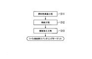
- the manufacturing method of the In—Cu sintered body sputtering target of this embodiment includes a raw material powder preparation step S11, a sintering step S12, and a machining step S13.
- the abundance of the In single phase is the peak intensity attributed to the (110) plane of the In single phase in the X-ray diffraction pattern, I (In), and the peak intensity attributed to the (111) plane of the Cu single phase, I ( Cu), the peak intensity attributed to the ( ⁇ 232) plane of the Cu7In3 phase is I (Cu7In3), the peak intensity attributed to the (200) plane of the Cu1In1 phase is I (Cu1In1), and the (313) plane of the Cu11In9 phase.
- the assigned peak intensity is I (Cu11In9)
- I (K compound) attributed to the K compound phase the following formula (1) Is a value calculated by.
- the maximum peak intensity I (Na compound) due to the Na compound is the (100) plane of the NaF phase when the Na compound is NaF, the (110) plane of the NaCl phase when NaCl is NaF, and the Na2S phase when Na2S is Na2S.
- the peak intensity is attributed to the (111) plane of the Na2Se phase.
- the maximum peak intensity I (K compound) due to the K compound phase is the (200) plane of the KF phase when the K compound is KF, the (110) plane of the KCl phase when K compound is KF, and the K2S when it is K2S.
- the (220) plane of the phase and in the case of K2Se, it is the peak intensity attributed to the (220) plane of the K2Se phase.
- the raw material powder is preferably either the following powder (1) or (2).
- In simple substance phase-containing In—Cu alloy powder or In powder the In content is less than 45 atomic%, the balance is composed of Cu and inevitable impurities, and there is an In simple substance phase.
- the In single-phase-containing In—Cu alloy powder (1) can be produced, for example, by a gas atomizing method. Specifically, it can be manufactured by preparing a Cu raw material and an In raw material, blending them so as to have the above-mentioned composition, dissolving them, pulverizing them by a gas atomizing method, and classifying them using a sieve having a pore diameter of 1000 ⁇ m. .
- the Cu raw material and the In raw material preferably have a purity of 99.99% by mass or more.
- the obtained In simple substance phase containing alloy powder it confirms that an In simple substance phase and a CuIn compound phase exist.
- a Cu raw material a Cu metal lump and Cu powder can be used.
- the In raw material In metal lump and In powder can be used.
- the ultimate vacuum at the time of Ar substitution is 10 Pa or less
- the melting temperature is 1100 ° C. or more and 1200 ° C. or less
- the injection temperature is 700 ° C. or more and 900 ° C. or less
- the injection gas pressure is 1.5 MPa or more. 9 MPa or less and the nozzle diameter are set to 0.5 mm or more and 3 mm or less.
- the gas atomization injection temperature is lower than 700 ° C., the ratio of CuIn compound phase generation increases, and the amount of In generated may decrease. For this reason, special attention is required when the In content is relatively low, 45 to 55 atomic%.
- the crucible is easily closed during atomization.
- the gas atomization injection temperature is set in the range of 700 ° C. or higher and 900 ° C. or lower.
- the gas atomization injection temperature is preferably set in the range of 750 ° C. or higher and 850 ° C. or lower, more preferably set in the range of 750 ° C. or higher and 800 ° C.
- the amount of oxygen in the manufactured In—Cu alloy powder can be set to 500 mass ppm or less.
- the ultimate vacuum at the time of Ar substitution is preferably 0.1 Pa or more and 5 Pa or less, and more preferably 0.5 Pa or more and 1 Pa or less, but is not limited thereto.
- the In simple substance phase-free In—Cu alloy powder used as the raw material of the powder mixture of the above (2) is prepared by preparing a Cu raw material and an In raw material, blending them to have the above-mentioned composition, It can be manufactured by pulverizing by a gas atomizing method and classifying using a sieve having a pore diameter of 1000 ⁇ m.
- the obtained In single-phase phase-free alloy powder it is confirmed that the In single-phase does not exist or even if it exists, its abundance is less than 5%. It can be confirmed by measuring the X-ray diffraction pattern of the alloy powder containing no In single phase that the In single phase does not exist or is less than 5%.
- the peak of the In single phase is not detected or the amount of the In single phase calculated by the equation (1) is less than 5%.
- that the peak of the In single phase is not detected means that the peak attributed to the (110) plane of the In single phase is not detected.
- the conditions for gas atomization are the same as those for producing the In single-phase-containing In—Cu alloy powder described above.
- the purity of the Cu powder and In powder used as the raw material of the powder mixture of the above (2) is 99.99 mass% or more.
- Cu powder and In powder are preferably classified using a sieve having a pore size of 1000 ⁇ m.
- the powder mixture of the above (2) comprises at least one of an In single-phase-containing In—Cu alloy powder or In powder, at least one of an In single-phase-free In—Cu alloy powder or Cu powder, and 10% In. It is prepared by mixing so that it is contained in the range of atomic% to 90 atomic% and the balance is composed of Cu and inevitable impurities.
- a mixing method a normal mixing apparatus used for mixing metal powders such as a ball mill and a rocking mixer can be used.
- the raw material powder prepared in the raw material powder preparation step S11 is hydrostatically pressurized at a temperature of 90 ° C. or higher and 140 ° C. or lower to form a sintered body.
- a method of forming the sintered body it is also possible to use hot press (uniaxial pressing) or HIP (hot isostatic pressing).
- HIP hot isostatic pressing
- the width of the pressure distribution at the time of pressing is large, and this width of the pressure distribution is reflected as a variation in the density of the obtained sintered body.
- a method of applying hydrostatic pressure at a temperature of 90 ° C. or higher and 140 ° C. or lower is employed.
- heating is performed at a relatively low temperature of 90 ° C. or more and 140 ° C. or less, In penetrates into the sintered body relatively uniformly, and a dense sintered body having a small density variation is obtained. It becomes possible.
- the pressure applied by hydrostatic pressure is preferably in the range of 100 MPa to 250 MPa, particularly preferably in the range of 150 MPa to 200 MPa.
- the In—Cu sintered sputtering target configured as described above, since relatively soft In is contained at 10 atomic% or more, generation of coarse chipping (chips) can be suppressed. The occurrence of abnormal discharge due to chipping traces can be suppressed.
- the In content is set to 90 atomic% or less, the amount of processing waste generated during processing such as cutting processing is reduced, and processing waste is less likely to adhere to the target surface after processing. Therefore, the processability is excellent.
- the theoretical density ratio is as high as 97% or more and is dense, it is possible to suppress the generation of cracks and chips during sputtering and processing, and to improve the workability with certainty. Furthermore, since the density variation is as low as 2% or less and the composition uniformity is high, the occurrence of abnormal discharge during sputtering can be suppressed.
- the variation of the In content is as small as 3% or less, the occurrence of abnormal discharge during sputtering is further suppressed, and the composition of the formed In—Cu alloy thin film becomes uniform. It becomes easy.
- the maximum particle size of the In single phase is relatively fine, 1 mm or less.
- the unevenness of the sputtering surface can be suppressed, and the occurrence of abnormal discharge during sputtering can be suppressed.
- the CuIn compound phase is harder than the In single phase, the presence of the CuIn compound phase improves the cutting workability.
- the maximum particle diameter of the CuIn compound phase is 150 ⁇ m or less, the occurrence of abnormal discharge due to chipping marks can be suppressed.
- the Na compound when the Na compound further contains one or more of NaF, NaCl, Na2S, and Na2Se, or as the K compound, one of KF, KCl, K2S, and K2Se Alternatively, when two or more types are contained, an In film containing an alkali metal can be formed. By forming a Cu—In—Ga—Se alloy thin film using this In film, it is possible to improve the conversion efficiency of the CIGS solar cell. Furthermore, since the maximum particle size of Na compound and K compound is limited to 15 ⁇ m or less, the occurrence of abnormal discharge during sputtering can be suppressed.
- the raw material powder includes the In single phase or In powder
- the In single phase or In powder In is It is easy to diffuse in the whole raw material powder relatively uniformly.
- In diffuses throughout the raw material powder it is possible to obtain a dense In—Cu sintered sputtering target with small variations in density.
- the In—Cu sintered sputtering target has been described as including an In single phase, but the present invention is not limited to this.
- the entire amount of In single phase or In powder contained in the raw material powder may be reacted with Cu to form a CuIn compound when the raw material powder is sintered into an In—Cu sintered body sputtering target.
- the maximum particle size of the CuIn compound phase may exceed 150 ⁇ m.
- the manufacturing method of the In—Cu sintered sputtering target is not limited to this embodiment, and may be manufactured by other manufacturing methods.
- the In—Cu alloy powder was manufactured as follows. A Cu metal mass having a purity of 99.99% by mass or more and an In metal mass having a purity of 99.99% by mass or more were weighed so that the contents of In and Cu were as shown in Table 1. The weighed raw materials were filled in a carbon crucible and dissolved, and then an In—Cu alloy powder was produced by a gas atomization method under the conditions of an injection temperature of 800 ° C., an injection gas pressure of 2.5 MPa, and a nozzle diameter of 1.5 mm. The amount of In single phase present in the produced In—Cu alloy powder was measured as follows. The results are shown in Table 1.
- the peak intensity I (In) attributed to the (110) plane of the In single phase and the peak intensity I (Cu) attributed to the (111) plane of the Cu single phase The peak intensity I (Cu7In3) attributed to the ( ⁇ 232) plane of the Cu7In3 phase, the peak intensity I (Cu1In1) attributed to the (200) plane of the Cu1In1 phase, and the (313) plane of the Cu11In9 phase.
- the peak intensity I (Cu11In9) was measured, and the abundance (%) of the In single phase was calculated by the above formula (1).
- Inventive Examples 1, 2, 3, 6, 7, 10 and Comparative Examples 1, 2, 3, 6, 9, 10 use In—Cu alloy powder as raw material powder.
- Invention Examples 4, 5, 8, and 9 and Comparative Examples 4, 5, 7, and 8 are such that the blending ratio when the total amount of the prepared powder is 100% by mass is the charging ratio in Table 1.
- Table 1 shows the composition of the raw material powder and the abundance of the In single phase.
- the composition of the raw material powder was calculated from the composition and blending ratio of the prepared powder.
- the amount of In single phase in the raw material powder was calculated from the X-ray diffraction pattern of the raw material powder.
- composition of In-Cu sintered sputtering target After fragments of the obtained In—Cu sintered sputtering target were pretreated with acid, composition analysis of In, Na, and K was performed by ICP-AES method. About Cu and other components, it described as a remainder. Since the measurement result was almost the same as the raw material powder of Table 1, the same numerical values as the composition ratio of the raw material powder of Table 1 are shown in Table 3.
- the cut-out cubic target pieces were equally divided into three in the thickness direction to obtain a total of 15 thin cubic target pieces (6.3 mm ⁇ 6.3 mm ⁇ 2 mmt).
- the size and weight were measured, and the measurement density was calculated. Table 3 shows the average values of the measured densities.
- the molten metal was melted by heating a powder having the same composition as that of the raw material powder used for the production of the In—Cu sintered sputtering target.
- the molten metal was cast and slowly cooled (cooling rate 5 ° C./min or less) to obtain an ingot (10 cm ⁇ 10 cm ⁇ 10 cm).
- the size and weight of the resulting ingot were measured to calculate the density, and this value was taken as the theoretical density.
- the In—Cu sintered body sputtering target contains NaF and KF
- the theoretical density was calculated from the respective theoretical densities and contents of InCu, NaF and KF as follows. The contents of InCu, NaF, and KF were calculated from the blending ratio of the raw materials.
- the theoretical density of InCu (InCu with a content ratio of In and Cu excluding NaF and KF) was measured by the above method, and the value was defined as Da (g / cm 3).
- the theoretical density of NaF was 2.79 (g / cm3), and the theoretical density of KF was 2.48 (g / cm3).
- the InCu content in the In—Cu sintered sputtering target is Wa (wt%), the NaF content is Wb (wt%), the KF content is Wc (wt%), and the theoretical density Db ( g / cm3) was calculated from the following formula.
- Db 100 / ⁇ (Wa / Da) + (Wb / 2.79) + (Wc / 2.48) ⁇
- Table 3 The results are shown in Table 3.
- Theoretical density ratio (%) ⁇ (measured density (average value)) / theoretical density ⁇ ⁇ 100
- Density variation (%) ⁇ (maximum value of density ⁇ minimum value of density) / average value of density ⁇ ⁇ 100
- CP processing is performed on the processed surface of the In—Cu sintered body sputtering target, and using a probe microanalyzer (EPMA) device (manufactured by JEOL Ltd.), Cu and In are magnified 1000 times.
- EMA probe microanalyzer
- Five element mapping images were taken, and from the element mapping images of Cu and In, a region where only In was present was defined as an In single phase. The diameter of the inscribed circle of the In single phase was measured, and this was used as the particle size of the In single phase.
- Comparative Example 6 in which the content of In exceeded the range of the present invention, the adhesion of the machining waste was observed during the lathe machining, and it took time for the machining. In Comparative Example 6, since the processing waste adhered, the number of abnormal discharges and the deviation of the In composition of the target during the sputter digging test were not measured. On the other hand, in Comparative Example 7 in which the In content is less than the range of the present invention, the theoretical density ratio was small, and coarse chipping occurred during lathe processing. In Comparative Example 7, since rough chipping occurred, the number of abnormal discharges and the deviation of the In composition of the target during the sputter digging test were not measured.
- Comparative Example 4 in which the maximum particle size of the Na compound was large, the number of abnormal discharges during sputtering was large, and sputtering could not be continued under high power conditions. Further, Comparative Example 5 having a large maximum particle size of the K compound was the same as that of Comparative Example 4.
- Example 10 of the present invention in which the In content, the theoretical density ratio, and the density variation are within the scope of the present invention, no adhesion of work scraps or generation of coarse chipping was observed during lathe processing, Excellent workability. In addition, it was confirmed that the number of abnormal discharges during sputtering was small and that stable sputtering film formation was possible. In Example 10 of the present invention in which the maximum particle size of the CuIn compound phase exceeds 150 ⁇ m, fine chipping of 0.5 mm occurs, but the number of abnormal discharges during sputtering is as small as 4 times, so this fine The occurrence of chipping is considered to be at a level that causes no problem in practical use. Furthermore, in Examples 8 and 9 of the present invention in which the maximum particle diameters of the Na compound and K compound were within the scope of the present invention, the number of abnormal discharges was reduced while containing the Na compound and K compound.
Landscapes
- Powder Metallurgy (AREA)
- Physical Vapour Deposition (AREA)
Abstract
Inを10原子%以上90原子%以下の範囲で含有し、残部がCu及び不可避不純物からなる組成を有し、理論密度比が97%以上であって、密度のばらつきが2%以内であることを特徴とするIn-Cu焼結体スパッタリングターゲット。
Description
本発明は、In-Cu合金の薄膜を成膜する際に用いられるIn-Cu焼結体スパッタリングターゲット、及びこのIn-Cu焼結体スパッタリングターゲットの製造方法に関するものである。
本願は、2017年3月23日に日本に出願された特願2017-057334号及び2018年2月14日に日本に出願された特願2018-024509号について優先権を主張し、その内容をここに援用する。
本願は、2017年3月23日に日本に出願された特願2017-057334号及び2018年2月14日に日本に出願された特願2018-024509号について優先権を主張し、その内容をここに援用する。
従来、化合物半導体からなる薄膜太陽電池として、Cu-In-Ga-Se系合金薄膜からなる光吸収層を備えたCIGS系太陽電池が広く提供されている。
ここで、Cu-In-Ga-Se系合金薄膜からなる光吸収層を形成する方法として、蒸着法により成膜する方法が知られている。蒸着法によって成膜された光吸収層を備えた太陽電池は、エネルギー交換効率が高いといった利点を有しているものの、成膜速度が遅く、生産効率が低いといった問題があった。
ここで、Cu-In-Ga-Se系合金薄膜からなる光吸収層を形成する方法として、蒸着法により成膜する方法が知られている。蒸着法によって成膜された光吸収層を備えた太陽電池は、エネルギー交換効率が高いといった利点を有しているものの、成膜速度が遅く、生産効率が低いといった問題があった。
そこで、Cu-In-Ga-Se系合金薄膜からなる光吸収層を形成する方法として、InとCuとGaを含む薄膜又はこれらの元素を含む薄膜の積層膜を形成し、この薄膜又は積層膜をSe雰囲気中で熱処理してセレン化する方法が提供されている。InとCuとGaを含む薄膜又はこれらの元素を含む薄膜の積層膜を形成する際には、各元素を含有したスパッタリングターゲットを用いたスパッタ法が適用される。
ここで、特許文献1には、0.5~7.5at%のCuを含むインジウムターゲットが提案されている。特許文献1には、インジウムターゲットの製造方法として、0.5~7.5at%のCuを含むインジウム合金を溶解鋳造する鋳造法が開示されている。
特許文献2には、30~80原子%のCuを含むIn-Cu合金スパッタリングターゲットが提案されている。この特許文献2の実施例では、純InターゲットにCuチップをチップオンしたスパッタリングを行ってIn-Cu合金膜を成膜している。
特許文献2には、30~80原子%のCuを含むIn-Cu合金スパッタリングターゲットが提案されている。この特許文献2の実施例では、純InターゲットにCuチップをチップオンしたスパッタリングを行ってIn-Cu合金膜を成膜している。
特許文献3には、銅とインジウムを含むスパッタリングターゲットの表面に、銅とインジウムを含む第1の相を有する粉末を冷間静水圧プレスして、修復されたターゲットを形成する方法が開示されている。この特許文献3の実施例では、銅とインジウムとガリウムを含む粉末が用いられている。
ところで、特許文献1に記載されたインジウムターゲットにおいては、Cuの含有量が少なく、In単体相が多く存在している。インジウムは、常温で非常に柔らかいことから、切削加工した際に、加工屑がターゲット表面に付着してしまう。このため、切削時に切削油を多量に供給したり、加工速度を遅くしたりする必要があった。
しかしながら、切削油を多量に供給した場合には、切削油成分が不純物として成膜した膜に混入するおそれがあった。切削油を除去するために洗浄工程を追加した場合には、工程が増え、生産コストが増大してしまう。また、加工速度を遅くした場合には、生産効率が低下してしまうといった問題があった。
しかしながら、切削油を多量に供給した場合には、切削油成分が不純物として成膜した膜に混入するおそれがあった。切削油を除去するために洗浄工程を追加した場合には、工程が増え、生産コストが増大してしまう。また、加工速度を遅くした場合には、生産効率が低下してしまうといった問題があった。
また、In-Cuスパッタリングターゲットの製造方法として、特許文献1に記載されている鋳造法では、Cuの一部が溶け残って異相となり易く、得られるインジウムターゲットに組成の偏析が生じ、密度のばらつきが大きくなるおそれがある。In-Cuスパッタリングターゲットに組成の偏析が生じ、密度のばらつきが大きいと、スパッタ時に異常放電が発生し易くなり、また成膜されたIn-Cu合金薄膜の組成ずれが生じる原因となるおそれがある。
特許文献2に記載されている純InターゲットにCuチップをチップオンしたスパッタリングでは、純Inターゲットの部分とCuチップの部分とでは導電性や密度が異なる。このため、スパッタ時に異常放電が発生し易くなり、また成膜レートが不安定となるので、成膜されたIn-Cu合金薄膜の組成ずれや膜厚のばらつきが生じる原因となるおそれがある。
特許文献3に記載されているCuとInを含む第1の相を有する粉末は、その粉末の組成によっては粉末単独では焼結しにくく、ターゲットの密度のばらつきが大きくなる場合があった。密度のばらつきが大きくなると、スパッタ時に異常放電が発生しやすくなり、また成膜レートが不安定となるので、成膜されたIn-Cu合金薄膜の組成ずれや膜厚のばらつきが生じる原因となるおそれがある。
特許文献3に記載されているCuとInを含む第1の相を有する粉末は、その粉末の組成によっては粉末単独では焼結しにくく、ターゲットの密度のばらつきが大きくなる場合があった。密度のばらつきが大きくなると、スパッタ時に異常放電が発生しやすくなり、また成膜レートが不安定となるので、成膜されたIn-Cu合金薄膜の組成ずれや膜厚のばらつきが生じる原因となるおそれがある。
この発明は、前述した事情に鑑みてなされたものであって、加工性に優れるとともに、スパッタ時の異常放電の発生を抑制することが可能なIn-Cuスパッタリングターゲット、及びこのIn-Cuスパッタリングターゲットの製造方法を提供することを目的とする。
上記課題を解決するために、本発明の一態様のIn-Cuスパッタリングターゲット(以下、「本発明のIn-Cuスパッタリングターゲット」と称します)は、In-Cu焼結体スパッタリングターゲットであり、Inを10原子%以上90原子%以下の範囲で含有し、残部がCuおよび不可避不純物からなる組成を有し、理論密度比が97%以上であって、密度のばらつきが2%以内であることを特徴としている。
上述の構成のn-Cu焼結体スパッタリングターゲットによれば、比較的柔らかいInを10原子%以上含有するので、1mmを超える粗大なチッピング(欠け)の発生を抑制できるとともに、チッピング跡に起因する異常放電の発生を抑制することができ、またターゲットの密度が高くなる。一方、Inの含有量が90原子%以下とされているので、切削加工などの加工によって発生する加工屑の発生量が少なくなり、ターゲット表面に加工屑が付着しにくくなる。よって、加工性が優れたものとなる。
さらに、理論密度比が97%以上と高く、緻密で、空孔が少ないためスパッタ時の異常放電や割れの発生を抑制することができる。またさらに、密度のばらつきが2%以内と低く、組成の均一性が高いので、スパッタ時の異常放電の発生をより抑制することができるとともに、成膜レートが安定するので、成膜されたIn-Cu合金薄膜は組成や膜厚が均一となり易くなる。
さらに、理論密度比が97%以上と高く、緻密で、空孔が少ないためスパッタ時の異常放電や割れの発生を抑制することができる。またさらに、密度のばらつきが2%以内と低く、組成の均一性が高いので、スパッタ時の異常放電の発生をより抑制することができるとともに、成膜レートが安定するので、成膜されたIn-Cu合金薄膜は組成や膜厚が均一となり易くなる。
ここで、本発明のIn-Cu焼結体スパッタリングターゲットにおいては、Inの含有量のばらつきが3%以内とされていることが好ましい。
この場合は、Inの含有量のばらつきが3%以内と少ないので、スパッタ時の異常放電の発生がさらに抑制されるとともに、成膜したIn-Cu合金薄膜の組成がより均一になり易くなる。
この場合は、Inの含有量のばらつきが3%以内と少ないので、スパッタ時の異常放電の発生がさらに抑制されるとともに、成膜したIn-Cu合金薄膜の組成がより均一になり易くなる。
また、本発明のIn-Cu焼結体スパッタリングターゲットにおいては、In単体相と、CuIn化合物相とが存在し、前記In単体相は最大粒子径が1mm以下であることが好ましい。
この場合、In単体相の最大粒子径が1mm以下と比較的微細とされているので、スパッタによってスパッタ面が消費された場合でも、スパッタ面の凹凸が抑えられ、スパッタ時の異常放電の発生を抑制することができる。
この場合、In単体相の最大粒子径が1mm以下と比較的微細とされているので、スパッタによってスパッタ面が消費された場合でも、スパッタ面の凹凸が抑えられ、スパッタ時の異常放電の発生を抑制することができる。
さらに、本発明のIn-Cu焼結体スパッタリングターゲットにおいては、さらにNa化合物としてNaF、NaCl、Na2S、Na2Seのうちの1種又は2種以上を含有し、このNa化合物の最大粒子径が15μm以下とされていることが好ましい。
この場合、上述のNa化合物を含有しているので、アルカリ金属であるNaを含むIn-Cu合金薄膜を成膜することができる。また、Na化合物の最大粒子径が15μm以下とされているので、スパッタ時の異常放電の発生を抑制できる。
この場合、上述のNa化合物を含有しているので、アルカリ金属であるNaを含むIn-Cu合金薄膜を成膜することができる。また、Na化合物の最大粒子径が15μm以下とされているので、スパッタ時の異常放電の発生を抑制できる。
またさらに、本発明のIn-Cu焼結体スパッタリングターゲットにおいては、さらにK化合物としてKF、KCl、K2S、K2Seのうちの1種又は2種以上を含有し、このK化合物の最大粒子径が15μm以下とされていることが好ましい。
この場合、上述のK化合物を含有しているので、アルカリ金属であるKを含むIn-Cu合金薄膜を成膜することができる。また、K化合物の最大粒子径が15μm以下とされているので、スパッタ時の異常放電の発生を抑制できる。
この場合、上述のK化合物を含有しているので、アルカリ金属であるKを含むIn-Cu合金薄膜を成膜することができる。また、K化合物の最大粒子径が15μm以下とされているので、スパッタ時の異常放電の発生を抑制できる。
本発明の他態様のIn-Cuスパッタリングターゲットの製造方法(以下、「本発明のIn-Cuスパッタリングターゲットの製造方法」と称する)は、上述のIn-Cu焼結体スパッタリングターゲットの製造方法であって、Inを10原子%以上90原子%以下の範囲で含有し、残部がCu及び不可避不純物からなる組成を有し、X線回折パターンにおけるIn単体相の(110)面に帰属されるピーク強度をI(In)、Cu単体相の(111)面に帰属されるピーク強度をI(Cu)、Cu7In3相の(-232)面に帰属されるピーク強度をI(Cu7In3)、Cu1In1相の(200)面に帰属されるピーク強度をI(Cu1In1)、Cu11In9相の(313)面に帰属されるピーク強度をI(Cu11In9)、Na化合物に起因する最大ピーク強度I(Na化合物)、K化合物相に起因する最大ピーク強度I(K化合物)とした場合に、下記の式(1)によって算出されるIn単体相の存在量が5%以上85%以下である原料粉を準備する原料粉準備工程と、
In単体相の存在量(%)=[I(In)/{I(Cu7In3)+I(Cu1In1)+I(Cu11In9)+I(In)+I(Cu)+I(Na化合物)+I(K化合物)}]×100・・・(1)
前記原料粉を90℃以上140℃以下の温度で静水圧加圧して、焼結させる焼結工程と、を備えていることを特徴としている。
In単体相の存在量(%)=[I(In)/{I(Cu7In3)+I(Cu1In1)+I(Cu11In9)+I(In)+I(Cu)+I(Na化合物)+I(K化合物)}]×100・・・(1)
前記原料粉を90℃以上140℃以下の温度で静水圧加圧して、焼結させる焼結工程と、を備えていることを特徴としている。
この構成のIn-Cu焼結体スパッタリングターゲットの製造方法によれば、原料粉が、融点が低いIn単体相を含むので、焼結工程において、In単体相のInが比較的均一に原料粉全体に拡散しやすい。このInが原料粉全体に拡散することによって、緻密でかつ密度のばらつきが小さいIn-Cu焼結体スパッタリングターゲットを得ることが可能となる。
本発明によれば、加工性に優れるとともに、スパッタ時の異常放電の発生を抑制することが可能なIn-Cu焼結体スパッタリングターゲット、及びこのIn-Cu焼結体スパッタリングターゲットの製造方法を提供することができる。
以下に、本発明の実施形態であるIn-Cu焼結体スパッタリングターゲット、及び、In-Cu焼結体スパッタリングターゲットの製造方法について、添付した図面を参照して説明する。
本実施形態に係るIn-Cu焼結体スパッタリングターゲットは、Inを10原子%以上90原子%以下の範囲で含有し、残部がCu及び不可避不純物からなる組成を有する。Inの含有量のばらつきは3%以内とされている。
さらに、理論密度比(上述の組成比から算出される理論密度に対する相対密度)が97%以上であって、密度のばらつきが2%以内とされている。
さらに、理論密度比(上述の組成比から算出される理論密度に対する相対密度)が97%以上であって、密度のばらつきが2%以内とされている。
そして、本実施形態に係るIn-Cu焼結体スパッタリングターゲットにおいては、In単体相とCuIn化合物相とが存在している。図1は、本発明の一実施形態に係るIn-Cu焼結体スパッタリングターゲットの元素分布図の一例であり、左図の白色の領域はCuIn化合物相、左図の黒色の領域はIn単体相を表している。図1に示すように、In単体相は、Inは検出されるが、Cuが検出されない領域を意味し、CuIn化合物相は、InとCuとが検出される領域を意味する。CuIn化合物相を構成するCuIn化合物は、Cu7In3、Cu1In1、Cu11In9等である。
ここで、In単体相の最大粒子径は1mm以下とされている。また、CuIn化合物相の最大粒子径は150μm以下とされている。
ここで、In単体相の最大粒子径は1mm以下とされている。また、CuIn化合物相の最大粒子径は150μm以下とされている。
また、本実施形態においては、さらにNa化合物としてNaF、NaCl、Na2S、Na2Seのうちの1種又は2種以上を含有し、このNa化合物の最大粒子径が15μm以下とされていてもよい。異常放電の抑制から、Na化合物の最大粒子径は、好ましくは10μm以下、より好ましくは5μm以下である。
また、さらにK化合物としてKF、KCl、K2S、K2Seのうちの1種又は2種以上を含有し、このK化合物の最大粒子径が15μm以下とされていてもよい。異常放電の抑制から、K化合物の最大粒子径は、好ましくは10μm以下、より好ましくは5μm以下である。
また、さらにK化合物としてKF、KCl、K2S、K2Seのうちの1種又は2種以上を含有し、このK化合物の最大粒子径が15μm以下とされていてもよい。異常放電の抑制から、K化合物の最大粒子径は、好ましくは10μm以下、より好ましくは5μm以下である。
以下に、本実施形態であるIn-Cu焼結体スパッタリングターゲットにおいて、Inの含有量とそのばらつき、理論密度比、密度のばらつき、In単体相とCuIn化合物相の最大粒子径、Na化合物およびK化合物について、上述のように規定した理由について説明する。
(Inの含有量:10原子%以上90原子%以下)
InにCuを添加することにより、Inよりも硬いCuIn化合物相が形成され、切削加工性を大幅に向上させることが可能となる。また、結晶粒径を微細化させることが可能となる。
ここで、Inの含有量が10原子%未満であると、In単体相が少なくなり、ターゲットの高密度が困難となるおそれがある。また、ターゲットが硬くなりすぎて、切削加工時に粗大なチッピングが発生する原因となる。また、このチッピング跡に起因する異常放電が発生するおそれがある。
一方、Inの含有量が90原子%を超えると、CuIn化合物相が十分に形成されず、切削加工性を向上させることができないおそれがある。
このような理由から、本実施形態においては、Inの含有量を10原子%以上90原子%以下の範囲内に設定している。異常放電発生の抑制の理由から、Inの含有量は、好ましくは20原子%以上80原子%以下である。
InにCuを添加することにより、Inよりも硬いCuIn化合物相が形成され、切削加工性を大幅に向上させることが可能となる。また、結晶粒径を微細化させることが可能となる。
ここで、Inの含有量が10原子%未満であると、In単体相が少なくなり、ターゲットの高密度が困難となるおそれがある。また、ターゲットが硬くなりすぎて、切削加工時に粗大なチッピングが発生する原因となる。また、このチッピング跡に起因する異常放電が発生するおそれがある。
一方、Inの含有量が90原子%を超えると、CuIn化合物相が十分に形成されず、切削加工性を向上させることができないおそれがある。
このような理由から、本実施形態においては、Inの含有量を10原子%以上90原子%以下の範囲内に設定している。異常放電発生の抑制の理由から、Inの含有量は、好ましくは20原子%以上80原子%以下である。
(Inの含有量のばらつき:3%以内)
Inの含有量のばらつきを小さくすることによって、膜組成が均一なIn-Cu合金薄膜を成膜することができる。
ここで、Inの含有量のばらつきが3%を超えると、成膜されるIn-Cu合金薄膜の組成のばらつきが大きくなるおそれがある。
Inの含有量のばらつきを小さくすることによって、膜組成が均一なIn-Cu合金薄膜を成膜することができる。
ここで、Inの含有量のばらつきが3%を超えると、成膜されるIn-Cu合金薄膜の組成のばらつきが大きくなるおそれがある。
ここで、本実施形態においては、In含有量のばらつきは、例えば、In-Cu焼結体スパッタリングターゲットのスパッタ面が図2に示すように、矩形の場合には、次のようにして測定する。スパッタ面の向かい合う角部を結ぶ対角線が交差する交点(1)と、各対角線上の角部から対角線の全長の10%以内の位置にある(2)、(3)、(4)、(5)の5点において、一辺の長さがスパッタ面の短辺の長さの5%となるように正方形状に切断して、立方体状のターゲット片を切り出す。切り出した立方体状のターゲット片を厚さ方向に3等分して、合計15個の薄型立方体状のターゲット片を得る。得られた薄型立方体状のターゲット片をそれぞれ分析試料として、In含有量をICP-AES法により測定する。測定したIn含有量の平均値を算出し、また測定したIn含有量の最大値と最小値をそれぞれ抽出する。In含有量のばらつきは、下記の式により求めた値とする。
In含有量のばらつき(%)={(In含有量の最大値-In含有量の最小値)/In含有量の平均値}×100
In含有量のばらつき(%)={(In含有量の最大値-In含有量の最小値)/In含有量の平均値}×100
なお、In-Cu焼結体スパッタリングターゲットのスパッタ面が図3に示すように、円形の場合には、分析試料として用いる薄型立方体状のターゲット片は次のようにして作製する。スパッタ面の中心(1)と、スパッタ面の中心を通過するとともに互いに直交する2本の直線上の外周部分から対角線の全長の10%以内の位置にある(2)、(3)、(4)、(5)の5点において、一辺の長さが、スパッタ面の直径の長さに対して5%となるように正方形状に切断して、立方体状のターゲット片を切り出す。切り出した立方体状のターゲット片を厚さ方向に3等分して、合計15個の薄型立方体状のターゲット片を得る。
(理論密度比:97%以上)
In-Cu焼結体スパッタリングターゲットの理論密度比が97%未満であると、空孔が多く存在することになり、スパッタ時に異常放電や割れが発生しやすくなるおそれがある。そこのため、本実施形態においては、理論密度比を97%以上に規定している。理論密度比は、通常100%以下である。
In-Cu焼結体スパッタリングターゲットの理論密度比が97%未満であると、空孔が多く存在することになり、スパッタ時に異常放電や割れが発生しやすくなるおそれがある。そこのため、本実施形態においては、理論密度比を97%以上に規定している。理論密度比は、通常100%以下である。
ここで、本実施形態において、理論密度は、下記の式により求めた値である。
理論密度比(%)=(測定密度/理論密度)×100
理論密度比(%)=(測定密度/理論密度)×100
なお、「測定密度」は、アルキメデス法を用いて測定する。
理論密度は、In、Cu、CuIn化合物の含有量比によって変動する。このため、本実施形態においては、InとCuの含有量比が、In-Cu焼結体スパッタリングターゲットと同じ割合の溶湯を溶製し、これを鋳造して徐冷(冷却速度5℃/min以下)することで得られた無欠陥の鋳塊(10cm×10cm×10cm)の密度を測定し、その値を「理論密度」とする。無欠陥の鋳塊であるか否かの確認は目視で行う。
理論密度は、In、Cu、CuIn化合物の含有量比によって変動する。このため、本実施形態においては、InとCuの含有量比が、In-Cu焼結体スパッタリングターゲットと同じ割合の溶湯を溶製し、これを鋳造して徐冷(冷却速度5℃/min以下)することで得られた無欠陥の鋳塊(10cm×10cm×10cm)の密度を測定し、その値を「理論密度」とする。無欠陥の鋳塊であるか否かの確認は目視で行う。
In-Cu焼結体スパッタリングターゲットがNa化合物、K化合物を含む場合は、これらの含有量によって、理論密度は変動する。このため、本実施形態においては、Na化合物、K化合物を含む場合は、InCu、Na化合物、K化合物のそれぞれの理論密度と含有量から理論密度を算出する。例えば、Na化合物としてNaF、K化合物としてKFを含むIn-Cu焼結体スパッタリングターゲットの理論密度は、下記の方法により算出できる。
まず、InCu(Na化合物とK化合物を除いたInとCuの含有量比のInCu)の理論密度を上記の方法で測定し、その値をDa(g/cm3)とする。また、NaFの理論密度を2.79(g/cm3)、KFの理論密度を2.48(g/cm3)とする。そして、In-Cu焼結体スパッタリングターゲット中のInCuの含有量をWa(wt%)、NaFの含有量をWb(wt%)、KFの含有量をWc(wt%)とし理論密度Db(g/cm3)を下記の計算式より算出する。
Db=100/{(Wa/Da)+(Wb/2.79)+(Wc/2.48)}
まず、InCu(Na化合物とK化合物を除いたInとCuの含有量比のInCu)の理論密度を上記の方法で測定し、その値をDa(g/cm3)とする。また、NaFの理論密度を2.79(g/cm3)、KFの理論密度を2.48(g/cm3)とする。そして、In-Cu焼結体スパッタリングターゲット中のInCuの含有量をWa(wt%)、NaFの含有量をWb(wt%)、KFの含有量をWc(wt%)とし理論密度Db(g/cm3)を下記の計算式より算出する。
Db=100/{(Wa/Da)+(Wb/2.79)+(Wc/2.48)}
(密度のばらつき:2%以下)
In-Cu焼結体スパッタリングターゲットの密度のばらつきを小さくすることによって、スパッタ時の異常放電の発生がより抑制され、またスパッタ時の成膜レートが安定する。
密度のばらつきが大きくなりすぎると、スパッタ時に異常放電が発生し易くなり、またスパッタ時の成膜レートが不安定となり、成膜されたIn-Cu合金薄膜は組成や膜厚が不均一となるおそれがある。このため、本実施形態においては、In-Cu焼結体スパッタリングターゲットの密度のばらつきを2%以下と設定している。異常放電発生の抑制の理由から、密度のばらつきは、好ましくは1.5%以下、より好ましくは1%以下である。
In-Cu焼結体スパッタリングターゲットの密度のばらつきを小さくすることによって、スパッタ時の異常放電の発生がより抑制され、またスパッタ時の成膜レートが安定する。
密度のばらつきが大きくなりすぎると、スパッタ時に異常放電が発生し易くなり、またスパッタ時の成膜レートが不安定となり、成膜されたIn-Cu合金薄膜は組成や膜厚が不均一となるおそれがある。このため、本実施形態においては、In-Cu焼結体スパッタリングターゲットの密度のばらつきを2%以下と設定している。異常放電発生の抑制の理由から、密度のばらつきは、好ましくは1.5%以下、より好ましくは1%以下である。
ここで、本実施形態において、密度のばらつきは、例えば、In-Cu焼結体スパッタリングターゲットのスパッタ面が図2に示すように、矩形の場合には、次のように測定する。スパッタ面の向かい合う角部を結ぶ対角線が交差する交点(1)と、各対角線上の角部から対角線の全長の10%以内の位置にある(2)、(3)、(4)、(5)の5点から、上記Inの含有量のばらつきの測定の場合と同様に、立方体状のターゲット片を切り出し、切り出した立方体状のターゲット片を厚さ方向に3等分して、合計15個の薄型立方体状のターゲット片を得る。得られた薄型立方体状のターゲット片をそれぞれ分析試料として、密度を、アルキメデス法を用いて測定する。測定した密度の平均値を算出し、また測定した密度の最大値と最小値をそれぞれ抽出する。密度のばらつきは、下記の式により求めた値とする。
密度のばらつき(%)={(密度の最大値-密度の最小値)/密度の平均値}×100
密度のばらつき(%)={(密度の最大値-密度の最小値)/密度の平均値}×100
なお、In-Cu焼結体スパッタリングターゲットのスパッタ面が図3に示すように、円形の場合には、上記Inの含有量のばらつきの測定の場合と同様に、スパッタ面の中心(1)と、スパッタ面の中心を通過するとともに互いに直交する2本の直線上の外周部分から対角線の全長の10%以内の位置にある(2)、(3)、(4)、(5)の5点から、立方体状のターゲット片を切り出し、切り出した立方体状のターゲット片を厚さ方向に3等分して、合計15個の薄型立方体状のターゲット片を得る。
(In単体相の最大粒子径:1mm以下)
本実施形態のIn-Cu焼結体スパッタリングターゲットにおいて、In単体相はCuIn化合物相とCuIn化合物相との間に存在し、両者を接合する作用を有する。In単体相が存在することによって、ターゲットの密度が高くなる。
このIn単体相の最大粒子径が1mmを超えて粗大になると、スパッタ時に異常放電が発生するおそれがある。このため、本実施形態においては、In単体相の最大粒子径を1mm以下と設定している。
なお、異常放電の発生を確実に抑制するためには、In単体相の最大粒子径を0.5mm以下とすることが好ましい。また、In単体相の最大粒子径の下限には特に制限はないが、0.010mm以上とすることが好ましい。
本実施形態のIn-Cu焼結体スパッタリングターゲットにおいて、In単体相はCuIn化合物相とCuIn化合物相との間に存在し、両者を接合する作用を有する。In単体相が存在することによって、ターゲットの密度が高くなる。
このIn単体相の最大粒子径が1mmを超えて粗大になると、スパッタ時に異常放電が発生するおそれがある。このため、本実施形態においては、In単体相の最大粒子径を1mm以下と設定している。
なお、異常放電の発生を確実に抑制するためには、In単体相の最大粒子径を0.5mm以下とすることが好ましい。また、In単体相の最大粒子径の下限には特に制限はないが、0.010mm以上とすることが好ましい。
(CuIn化合物相の最大粒子径:150μm以下)
CuIn化合物相は、In単体相よりも硬い。このためCuIn化合物相が存在することにより、切削加工性が向上することになる。
このCuIn化合物相の最大粒子径が150μmを超えて粗大になると、切削加工時に粗大なチッピングが発生する原因となる。また、このチッピング跡に起因する異常放電が発生するおそれがある。このような理由から、本実施形態においては、CuIn化合物相の最大粒子径を150μm以下と設定している。
なお、チッピングの発生を確実に抑制するためには、CuIn化合物相の最大粒子径を100μm以下とすることが好ましく、50μm以下とするとさらに好ましい。また、CuIn化合物相の最大粒子径の下限には特に制限はないが、切削加工性を確実に向上させるためには、1μm以上とすることが好ましい。
CuIn化合物相は、In単体相よりも硬い。このためCuIn化合物相が存在することにより、切削加工性が向上することになる。
このCuIn化合物相の最大粒子径が150μmを超えて粗大になると、切削加工時に粗大なチッピングが発生する原因となる。また、このチッピング跡に起因する異常放電が発生するおそれがある。このような理由から、本実施形態においては、CuIn化合物相の最大粒子径を150μm以下と設定している。
なお、チッピングの発生を確実に抑制するためには、CuIn化合物相の最大粒子径を100μm以下とすることが好ましく、50μm以下とするとさらに好ましい。また、CuIn化合物相の最大粒子径の下限には特に制限はないが、切削加工性を確実に向上させるためには、1μm以上とすることが好ましい。
(Na化合物及びK化合物:最大粒子径15μm以下)
スパッタリングターゲットに、Na化合物あるいはK化合物を含有させることにより、成膜されたIn膜中にアルカリ金属を含有させることができる。ここで、Cu-In-Ga-Se系合金薄膜を光吸収層として有する太陽電池においては、Cu-In-Ga-Se系合金薄膜にアルカリ金属を添加することにより、変換効率が大きく向上することになる。このため、本実施形態であるスパッタリングターゲットに、Na化合物あるいはK化合物を含有させてもよい。なお、Na化合物及びK化合物の含有量については、全ての金属元素の含有量としてそれぞれNa及びKの含有量が0.1原子%以上10原子%の範囲内とすることが好ましく、0.1原子%以上5原子%の範囲内とすることがさらに好ましい。0.1原子%未満の場合には添加による変換効率の向上効果が得られにくくなり、10原子%を超える場合にはNa化合物あるいはK化合物に起因する異常放電が多発し、スパッタが困難となるおそれがある。
ここで、Na化合物あるいはK化合物の最大粒子径が15μmを超えると、スパッタ時に異常放電が発生するおそれがある。このため、本実施形態では、Na化合物及びK化合物を含有させる場合には、これらの最大粒子径を15μm以下に制限している。
スパッタリングターゲットに、Na化合物あるいはK化合物を含有させることにより、成膜されたIn膜中にアルカリ金属を含有させることができる。ここで、Cu-In-Ga-Se系合金薄膜を光吸収層として有する太陽電池においては、Cu-In-Ga-Se系合金薄膜にアルカリ金属を添加することにより、変換効率が大きく向上することになる。このため、本実施形態であるスパッタリングターゲットに、Na化合物あるいはK化合物を含有させてもよい。なお、Na化合物及びK化合物の含有量については、全ての金属元素の含有量としてそれぞれNa及びKの含有量が0.1原子%以上10原子%の範囲内とすることが好ましく、0.1原子%以上5原子%の範囲内とすることがさらに好ましい。0.1原子%未満の場合には添加による変換効率の向上効果が得られにくくなり、10原子%を超える場合にはNa化合物あるいはK化合物に起因する異常放電が多発し、スパッタが困難となるおそれがある。
ここで、Na化合物あるいはK化合物の最大粒子径が15μmを超えると、スパッタ時に異常放電が発生するおそれがある。このため、本実施形態では、Na化合物及びK化合物を含有させる場合には、これらの最大粒子径を15μm以下に制限している。
次に、本実施形態に係るIn-Cu焼結体スパッタリングターゲットの製造方法について、図4のフロー図を参照して説明する。本実施形態のIn-Cu焼結体スパッタリングターゲットの製造方法は、原料粉準備工程S11、焼結工程S12、機械加工工程S13を備える。
(原料粉準備工程S11)
原料粉準備工程S11では、Inを10原子%以上90原子%以下の範囲で含有し、残部がCu及び不可避不純物からなる組成を有し、In単体相の存在量が5%以上85%以下である原料粉を準備する。
原料粉準備工程S11では、Inを10原子%以上90原子%以下の範囲で含有し、残部がCu及び不可避不純物からなる組成を有し、In単体相の存在量が5%以上85%以下である原料粉を準備する。
In単体相の存在量は、X線回折パターンにおけるIn単体相の(110)面に帰属されるピーク強度をI(In)、Cu単体相の(111)面に帰属されるピーク強度をI(Cu)、Cu7In3相の(-232)面に帰属されるピーク強度をI(Cu7In3)、Cu1In1相の(200)面に帰属されるピーク強度をI(Cu1In1)、Cu11In9相の(313)面に帰属されるピーク強度をI(Cu11In9)、Na化合物に起因する最大ピーク強度I(Na化合物)、K化合物相に起因する最大ピーク強度I(K化合物)とした場合に、下記の式(1)によって算出される値である。
In単体相の存在量(%)=[I(In)/{I(Cu7In3)+I(Cu1In1)+I(Cu11In9)+I(In)+I(Cu)+I(Na化合物)+I(K化合物)}]×100・・・(1)
In単体相の存在量(%)=[I(In)/{I(Cu7In3)+I(Cu1In1)+I(Cu11In9)+I(In)+I(Cu)+I(Na化合物)+I(K化合物)}]×100・・・(1)
なお、Na化合物に起因する最大ピーク強度I(Na化合物)は、Na化合物がNaFの場合はNaF相の(100)面、NaClの場合はNaCl相の(110)面、Na2Sの場合はNa2S相の(220)面、Na2Seの場合はNa2Se相の(111)面にそれぞれ帰属されるピーク強度である。また、K化合物相に起因する最大ピーク強度I(K化合物)は、K化合物がKFの場合はKF相の(200)面、KClの場合はKCl相の(110)面、K2Sの場合はK2S相の(220)面、K2Seの場合はK2Se相の(220)面にそれぞれ帰属されるピーク強度である。
原料粉は、以下の粉末(1)もしくは(2)のいずれかであることが好ましい。
(1)Inを45原子%以上90原子%以下の範囲で含有し、残部がCu及び不可避不純物からなる組成を有し、In単体相の存在量が5%以上85%以下であるIn-Cu合金粉末(In単体相含有In-Cu合金粉末)
(2)In単体相含有In-Cu合金粉末またはIn粉末のうち少なくとも一方と、Inの含有量が45原子%未満で、残部がCuおよび不可避不純物からなる組成を有し、In単体相が存在しないか、あるいは存在しているとしてもその存在量が5%未満であるIn-Cu合金粉末(In単体相不含有In-Cu合金粉末)またはCu粉末のうち少なくとも一方とを、Inを10原子%以上90原子%以下の範囲で含有し、残部がCuおよび不可避不純物からなる組成となるように含む粉末混合物
(1)Inを45原子%以上90原子%以下の範囲で含有し、残部がCu及び不可避不純物からなる組成を有し、In単体相の存在量が5%以上85%以下であるIn-Cu合金粉末(In単体相含有In-Cu合金粉末)
(2)In単体相含有In-Cu合金粉末またはIn粉末のうち少なくとも一方と、Inの含有量が45原子%未満で、残部がCuおよび不可避不純物からなる組成を有し、In単体相が存在しないか、あるいは存在しているとしてもその存在量が5%未満であるIn-Cu合金粉末(In単体相不含有In-Cu合金粉末)またはCu粉末のうち少なくとも一方とを、Inを10原子%以上90原子%以下の範囲で含有し、残部がCuおよび不可避不純物からなる組成となるように含む粉末混合物
上記(1)のIn単体相含有In-Cu合金粉末は、例えば、ガスアトマイズ法によって製造することができる。具体的には、Cu原料とIn原料を準備し、上述の組成となるように配合して溶解後、ガスアトマイズ法によって粉状化し、孔径1000μmの篩を用いて分級することによって製造することができる。Cu原料およびIn原料は、純度が99.99質量%以上であることが好ましい。なお、得られたIn単体相含有合金粉末については、In単体相およびCuIn化合物相が存在することを確認する。Cu原料としては、Cu金属塊およびCu粉を使用できる。また、In原料としては、In金属塊およびIn粉を使用できる。
ガスアトマイズの条件としては、Ar置換の際の到達真空度を10Pa以下、溶解時の温度を1100℃以上1200℃以下、噴射温度を700℃以上900℃以下、噴射ガス圧を1.5MPa以上3.9MPa以下、ノズル径を0.5mm以上3mm以下と設定する。ここで、ガスアトマイズの噴射温度が700℃未満の場合、CuIn化合物相の生成の割合が増加し、Inの生成量が低下するおそれがある。このため、Inの含有量が45~55原子%と比較的少ない場合には、特に注意が必要である。また、アトマイズ時にるつぼが閉塞しやすくなる。一方、噴射温度が900℃を超えると、得られる原料粉のInの割合がIn-Cu状態図から得られる割合に比べて多くなり、CuIn化合物相が不足し、切削加工性が向上しないおそれがある。また、アトマイズ時にチャンバー内に粉が付着し、粉の収率が低下するおそれがある。以上のことから、本実施形態では、ガスアトマイズの噴射温度を700℃以上900℃以下の範囲内に設定している。ガスアトマイズの噴射温度は、750℃以上850℃以下の範囲内に設定することが好ましく、750℃以上800℃以下の範囲内に設定することがより好ましいが、これに限定されることはない。また、Ar置換の際の到達真空度を10Pa以下とすることで、製造されたIn-Cu合金粉中の酸素量を500質量ppm以下にすることが可能となる。Ar置換の際の到達真空度は、0.1Pa以上5Pa以下にすることが好ましく、0.5Pa以上1Pa以下にすることがより好ましいが、これに限定されることはない。
上記(2)の粉末混合物の原料として用いるIn単体相不含有In-Cu合金粉末は、具体的には、Cu原料とIn原料を準備し、上述の組成となるように配合して溶解後、ガスアトマイズ法によって粉状化し、孔径1000μmの篩を用いて分級することによって製造することができる。なお、得られたIn単体相不含有合金粉末については、In単体相が存在しないか、あるいは存在しているとしてもその存在量が5%未満であることを確認する。In単体相が存在しないか、あるいはその存在量が5%未満であることは、In単体相不含有合金粉末のX線回折パターンを測定することによって確認することができる。すなわち、X線回折パターンにおいて、In単体相のピークが検出されないか、上記(1)の式で算出されるIn単体相の存在量が5%未満であることを確認する。ここで、In単体相のピークが検出されないとは、In単体相の(110)面に帰属されるピークが検出されないことを意味する。
ガスアトマイズの条件は、上述のIn単体相含有In-Cu合金粉末を製造する場合の条件と同じである。
ガスアトマイズの条件は、上述のIn単体相含有In-Cu合金粉末を製造する場合の条件と同じである。
上記(2)の粉末混合物の原料として用いるCu粉末およびIn粉末は、純度が99.99質量%以上であることが好ましい。Cu粉末およびIn粉末は、孔径1000μmの篩を用いて分級することが好ましい。
上記(2)の粉末混合物は、In単体相含有In-Cu合金粉末またはIn粉末のうち少なくとも一方と、In単体相不含有In-Cu合金粉末またはCu粉末のうち少なくとも一方とを、Inを10原子%以上90原子%以下の範囲で含有し、残部がCuおよび不可避不純物からなる組成となるように混合することによって調製する。混合方法としては、ボールミルおよびロッキングミキサーなどの金属粉末の混合に用いられる通常の混合装置を用いることができる。
(焼結工程)
焼結工程S12では、上記原料粉準備工程S11にて準備した原料粉を、90℃以上140℃以下の温度で静水圧加圧を行って、焼結体を形成する。
ここで、焼結体を形成する方法として、ホットプレス(一軸加圧)やHIP(熱間等方圧加圧)を利用することも考えられる。しかし、ホットプレスでは、プレス時の圧力分布の幅が大きく、この圧力分布の幅が、得られる焼結体の密度のばらつきとして反映され、特にスパッタ面の面積が600cm2以上の大型の焼結体(In-Cu焼結体スパッタリングターゲット)では密度のばらつきが大きくなるおそれがある。また、密度のばらつきを抑えるため、200MPaの高圧力を付与することが考えられるが、例えば、ターゲットの面積が600cm2以上の大型の焼結体を製造する場合には、約1200tonプレス機が必要となり、装置が大掛かりになり、工業的に不利になる。
焼結工程S12では、上記原料粉準備工程S11にて準備した原料粉を、90℃以上140℃以下の温度で静水圧加圧を行って、焼結体を形成する。
ここで、焼結体を形成する方法として、ホットプレス(一軸加圧)やHIP(熱間等方圧加圧)を利用することも考えられる。しかし、ホットプレスでは、プレス時の圧力分布の幅が大きく、この圧力分布の幅が、得られる焼結体の密度のばらつきとして反映され、特にスパッタ面の面積が600cm2以上の大型の焼結体(In-Cu焼結体スパッタリングターゲット)では密度のばらつきが大きくなるおそれがある。また、密度のばらつきを抑えるため、200MPaの高圧力を付与することが考えられるが、例えば、ターゲットの面積が600cm2以上の大型の焼結体を製造する場合には、約1200tonプレス機が必要となり、装置が大掛かりになり、工業的に不利になる。
一方、HIPでは、通常のオイル等の媒体がガス化することで加熱と加圧を同時に行っているため、比較的低温での温度制御が困難である。これに対して、Inは、軟化点が90℃で融点が156.4℃と比較的低温である。このため、HIPでは温度のむらによって、Inが溶出したり、Inが偏在することによって、得られる焼結体の密度のばらつきが大きくなるおそれがある。
以上のような理由から、本実施形態では、90℃以上140℃以下の温度で静水圧加圧する方法を採用している。本実施形態では90℃以上140℃以下と比較的低い温度で加熱しているので、Inが比較的均一に焼結体の内部に浸透し、緻密でかつ密度のばらつきが小さい焼結体を得ることが可能となる。静水圧加圧による加圧の圧力は、好ましくは100MPa以上250MPa以下の範囲にあり、特に好ましくは150MPa以上200MPa以下の範囲である。
(機械加工工程)
機械加工工程S13では、上記焼結工程S12で得られた焼結体に対して、旋盤加工、フライス加工等を行う。これにより、所定形状のIn-Cu焼結体スパッタリングターゲットを得る。
機械加工工程S13では、上記焼結工程S12で得られた焼結体に対して、旋盤加工、フライス加工等を行う。これにより、所定形状のIn-Cu焼結体スパッタリングターゲットを得る。
以上のような構成とされた本実施形態に係るIn-Cu焼結体スパッタリングターゲットによれば、比較的柔らかいInを10原子%以上含有するので、粗大なチッピング(欠け)の発生を抑制できるとともに、チッピング跡に起因する異常放電の発生を抑制することができる。また、Inの含有量が90原子%以下とされているので、切削加工などの加工時に発生する加工屑の発生量が少なくなり、加工後のターゲット表面に加工屑が付着しにくくなる。よって、加工性が優れたものとなる。
また、理論密度比が97%以上と高く、緻密であるため、スパッタ時および加工時での割れや欠けの発生を抑制できるとともに、加工性を確実に向上させることが可能となる。さらに、密度のばらつきが2%以内と低く、組成の均一性が高いので、スパッタ時の異常放電の発生を抑制することができる。
また、理論密度比が97%以上と高く、緻密であるため、スパッタ時および加工時での割れや欠けの発生を抑制できるとともに、加工性を確実に向上させることが可能となる。さらに、密度のばらつきが2%以内と低く、組成の均一性が高いので、スパッタ時の異常放電の発生を抑制することができる。
また、本実施形態においては、Inの含有量のばらつきが3%以内と少ないので、スパッタ時の異常放電の発生がさらに抑制されるとともに、成膜したIn-Cu合金薄膜の組成が均一になり易くなる。
さらに、本実施形態においては、In単体相とCuIn化合物相とが存在し、前記In単体相の最大粒子径が1mm以下と比較的微細とされているので、スパッタによってスパッタ面が消費された場合でも、スパッタ面の凹凸が抑えられ、スパッタ時の異常放電の発生を抑制することができる。また、CuIn化合物相は、In単体相よりも硬いので、CuIn化合物相が存在することにより、切削加工性が向上することになる。さらにCuIn化合物相の最大粒子径が150μm以下とされているので、チッピング跡に起因する異常放電の発生を抑制することができる。
またさらに、本実施形態において、さらにNa化合物としてNaF、NaCl、Na2S、Na2Seのうちの1種又は2種以上を含有する場合、あるいはさらにK化合物としてKF、KCl、K2S、K2Seのうちの1種又は2種以上を含有する場合には、アルカリ金属を含むIn膜を成膜することができる。このIn膜を用いてCu-In-Ga-Se系合金薄膜を成膜することで、CIGS系太陽電池の変換効率を向上させることが可能となる。
さらに、Na化合物及びK化合物の最大粒子径が15μm以下に制限されているので、スパッタ時の異常放電の発生を抑制することができる。
さらに、Na化合物及びK化合物の最大粒子径が15μm以下に制限されているので、スパッタ時の異常放電の発生を抑制することができる。
また、本実施形態のIn-Cu焼結体スパッタリングターゲットの製造方法によれば、原料粉がIn単体相もしくはIn粉末を含むので、焼結工程S12において、In単体相もしくはIn粉末のInが、比較的均一に原料粉全体に拡散しやすい。このInが原料粉全体に拡散することによって、緻密でかつ密度のばらつきが小さいIn-Cu焼結体スパッタリングターゲットを得ることが可能となる。
以上、本発明の実施形態について説明したが、本発明はこれに限定されることはなく、その発明の技術的思想を逸脱しない範囲で適宜変更可能である。
例えば、本実施形態では、In-Cu焼結体スパッタリングターゲットは、In単体相を含むものとして説明したが、これに限定されることはない。例えば、原料粉に含まれているIn単体相あるいはIn粉末の全量を、原料粉を焼結させてIn-Cu焼結体スパッタリングターゲットとする際に、Cuと反応させてCuIn化合物としてもよい。また、CuIn化合物相の最大粒子径は、150μmを超えていてもよい。
例えば、本実施形態では、In-Cu焼結体スパッタリングターゲットは、In単体相を含むものとして説明したが、これに限定されることはない。例えば、原料粉に含まれているIn単体相あるいはIn粉末の全量を、原料粉を焼結させてIn-Cu焼結体スパッタリングターゲットとする際に、Cuと反応させてCuIn化合物としてもよい。また、CuIn化合物相の最大粒子径は、150μmを超えていてもよい。
さらに、In-Cu焼結体スパッタリングターゲットの製造方法については、本実施形態に限定されることはなく、他の製造方法によって製造されたものであってもよい。
[本発明例1~10、比較例1~10]
(1)原料粉準備工程
表1に示すように、In-Cu合金粉末(本発明例1~4、6~10、比較例1~6、8~10)、In粉末(本発明例5、比較例7)、Cu粉末(本発明例4、5、比較例7、8)、Na化合物粉末(本発明例8、比較例4)、K化合物粉末(本発明例9、比較例5)を用意した。In粉末は、純度99.99質量%以上である。Cu粉末は、純度99.99質量%以上である。
(1)原料粉準備工程
表1に示すように、In-Cu合金粉末(本発明例1~4、6~10、比較例1~6、8~10)、In粉末(本発明例5、比較例7)、Cu粉末(本発明例4、5、比較例7、8)、Na化合物粉末(本発明例8、比較例4)、K化合物粉末(本発明例9、比較例5)を用意した。In粉末は、純度99.99質量%以上である。Cu粉末は、純度99.99質量%以上である。
In-Cu合金粉末は、次のようにして製造した。
純度99.99質量%以上のCu金属塊と、純度99.99質量%以上のIn金属塊を、InとCuの含有量が表1に示す組成となるように秤量した。秤量した原料を、カーボン坩堝に充填して溶解した後、噴射温度800℃、噴射ガス圧2.5MPa、ノズル径1.5mmの条件にてガスアトマイズ法により、In-Cu合金粉末を作製した。作製したIn-Cu合金粉末のIn単体相の存在量を、下記のようにして測定した。その結果を表1に示す。
純度99.99質量%以上のCu金属塊と、純度99.99質量%以上のIn金属塊を、InとCuの含有量が表1に示す組成となるように秤量した。秤量した原料を、カーボン坩堝に充填して溶解した後、噴射温度800℃、噴射ガス圧2.5MPa、ノズル径1.5mmの条件にてガスアトマイズ法により、In-Cu合金粉末を作製した。作製したIn-Cu合金粉末のIn単体相の存在量を、下記のようにして測定した。その結果を表1に示す。
(In単体相の存在量)
In-Cu合金粉末のX線回折パターンを以下の条件で測定した。
装置:理学電気社製(RINT-Ultima/PC)
管球:Cu
管電圧:40kV
管電流:40mA
走査範囲(2θ):10°~80°
スリットサイズ:発散(DS)2/3度、散乱(SS)2/3度、受光(RS)0.8mm
測定ステップ幅:2θで0.02度
スキャンスピード:毎分2度
試料台回転スピード:30rpm
In-Cu合金粉末のX線回折パターンを以下の条件で測定した。
装置:理学電気社製(RINT-Ultima/PC)
管球:Cu
管電圧:40kV
管電流:40mA
走査範囲(2θ):10°~80°
スリットサイズ:発散(DS)2/3度、散乱(SS)2/3度、受光(RS)0.8mm
測定ステップ幅:2θで0.02度
スキャンスピード:毎分2度
試料台回転スピード:30rpm
以上の条件で測定したX線回折パターンにおけるIn単体相の(110)面に帰属されるピーク強度I(In)と、Cu単体相の(111)面に帰属されるピーク強度I(Cu)と、Cu7In3相の(-232)面に帰属されるピーク強度I(Cu7In3)と、Cu1In1相の(200)面に帰属されるピーク強度I(Cu1In1)と、Cu11In9相の(313)面に帰属されるピーク強度I(Cu11In9)をそれぞれ計測し、In単体相の存在量(%)を前記の式(1)にて算出した。
本発明例1、2、3、6、7、10および比較例1、2、3、6、9、10は、In-Cu合金粉末を原料粉とした。
本発明例4、5、8、9および比較例4、5、7、8は、用意した粉末を、全体量を100質量%としたときの配合割合が、表1の投入割合となるように秤量し、秤量した各粉末を混合し、得られた粉末混合物を原料粉とした。粉末の混合は、ボールミルを用いた。
原料粉の組成とIn単体相の存在量を表1に示す。なお、原料粉の組成は、用意した粉末の組成と配合割合から算出した。原料粉のIn単体相の存在量は、原料粉のX線回折パターンから算出した。
本発明例4、5、8、9および比較例4、5、7、8は、用意した粉末を、全体量を100質量%としたときの配合割合が、表1の投入割合となるように秤量し、秤量した各粉末を混合し、得られた粉末混合物を原料粉とした。粉末の混合は、ボールミルを用いた。
原料粉の組成とIn単体相の存在量を表1に示す。なお、原料粉の組成は、用意した粉末の組成と配合割合から算出した。原料粉のIn単体相の存在量は、原料粉のX線回折パターンから算出した。
(2)焼結工程
上記(1)原料粉準備工程で調製した原料粉を、モールドに充填して、表2に示す焼結条件にて加熱して、焼結させた。
上記(1)原料粉準備工程で調製した原料粉を、モールドに充填して、表2に示す焼結条件にて加熱して、焼結させた。
(3)機械加工工程
上記(2)焼結工程で得られた焼結体を、旋盤とフライス盤とを用いて126mm×178mm×6mmtサイズのIn-Cu焼結体スパッタリングターゲットに加工した。
上記(2)焼結工程で得られた焼結体を、旋盤とフライス盤とを用いて126mm×178mm×6mmtサイズのIn-Cu焼結体スパッタリングターゲットに加工した。
(In-Cu焼結体スパッタリングターゲットの組成)
得られたIn-Cu焼結体スパッタリングターゲットの破片を酸で前処理した後、ICP-AES法によりIn、Na、Kの組成分析を行った。Cu及びその他の成分については、残部として記載した。測定結果は表1の原料粉とほぼ同じであった為、表1の原料粉の組成比と同じ数値を表3に記載した。
得られたIn-Cu焼結体スパッタリングターゲットの破片を酸で前処理した後、ICP-AES法によりIn、Na、Kの組成分析を行った。Cu及びその他の成分については、残部として記載した。測定結果は表1の原料粉とほぼ同じであった為、表1の原料粉の組成比と同じ数値を表3に記載した。
(密度)
図2に示すように、In-Cu焼結体スパッタリングターゲットのスパッタ面の向かい合う角部を結ぶ対角線が交差する交点(1)と、各対角線上の角部から対角線の全長の10%以内の位置にある(2)、(3)、(4)、(5)の5点において、一辺の長さが6.3mm(=126mm×5%)の正方形状に切断して、立方体状のターゲット片を切り出した。切り出した立方体状のターゲット片を厚さ方向に3等分して、合計15個の薄型立方体状のターゲット片(6.3mm×6.3mm×2mmt)を得た。得られた薄型立方体状のターゲット片をそれぞれ分析試料として、サイズと重量を測定し、測定密度を算出した。測定密度の平均値を表3に示す。
図2に示すように、In-Cu焼結体スパッタリングターゲットのスパッタ面の向かい合う角部を結ぶ対角線が交差する交点(1)と、各対角線上の角部から対角線の全長の10%以内の位置にある(2)、(3)、(4)、(5)の5点において、一辺の長さが6.3mm(=126mm×5%)の正方形状に切断して、立方体状のターゲット片を切り出した。切り出した立方体状のターゲット片を厚さ方向に3等分して、合計15個の薄型立方体状のターゲット片(6.3mm×6.3mm×2mmt)を得た。得られた薄型立方体状のターゲット片をそれぞれ分析試料として、サイズと重量を測定し、測定密度を算出した。測定密度の平均値を表3に示す。
また、In-Cu焼結体スパッタリングターゲットの製造に用いた原料粉と同じ組成の粉末を加熱して、溶湯を溶製した。次いで溶製した溶湯を鋳造し、徐冷(冷却速度5℃/min以下)して鋳塊(10cm×10cm×10cm)を得た。得られた鋳塊のサイズと重量を測定して、密度を算出し、この値を理論密度とした。なお、In-Cu焼結体スパッタリングターゲットがNaF、KFを含む場合は、InCu、NaF、KFのそれぞれの理論密度と含有量から次のようにして理論密度を算出した。なお、InCu、NaF、KFの含有量は、原料の配合割合から算出した。
まず、InCu(NaFとKFを除いたInとCuの含有量比のInCu)の理論密度を上記の方法で測定し、その値をDa(g/cm3)とした。NaFの理論密度を2.79(g/cm3)、KFの理論密度を2.48(g/cm3)とした。そして、In-Cu焼結体スパッタリングターゲット中のInCuの含有量をWa(wt%)、NaFの含有量をWb(wt%)、KFの含有量をWc(wt%)とし、理論密度Db(g/cm3)を下記の計算式より算出した。
Db=100/{(Wa/Da)+(Wb/2.79)+(Wc/2.48)}
その結果を表3に示す。
まず、InCu(NaFとKFを除いたInとCuの含有量比のInCu)の理論密度を上記の方法で測定し、その値をDa(g/cm3)とした。NaFの理論密度を2.79(g/cm3)、KFの理論密度を2.48(g/cm3)とした。そして、In-Cu焼結体スパッタリングターゲット中のInCuの含有量をWa(wt%)、NaFの含有量をWb(wt%)、KFの含有量をWc(wt%)とし、理論密度Db(g/cm3)を下記の計算式より算出した。
Db=100/{(Wa/Da)+(Wb/2.79)+(Wc/2.48)}
その結果を表3に示す。
上記の測定密度の平均値と理論密度とを用いて、下記の式より理論密度比を算出した。その結果を表3に示す。
理論密度比(%)={(測定密度(平均値))/理論密度}×100
理論密度比(%)={(測定密度(平均値))/理論密度}×100
さらに、測定密度の最大値と最小値とを抽出し、下記の式より密度のばらつきを算出した。その結果を表3に示す。
密度のばらつき(%)={(密度の最大値-密度の最小値)/密度の平均値}×100
密度のばらつき(%)={(密度の最大値-密度の最小値)/密度の平均値}×100
(In含有量のばらつき)
上記の密度の測定で得られた薄型立方体状のターゲット片を分析試料としてそれぞれ酸で前処理した後、ICP-AES法によりInの含有量を測定した。次いで、測定したIn含有量の最大値と最小値をそれぞれ抽出し、また全てのIn含有量の平均値を算出した。そして、In含有量のばらつきを、下記の式により算出した。その結果を表3に示す。
In含有量のばらつき(%)={(In含有量の最大値-In含有量の最小値)/In含有量の平均値}×100
上記の密度の測定で得られた薄型立方体状のターゲット片を分析試料としてそれぞれ酸で前処理した後、ICP-AES法によりInの含有量を測定した。次いで、測定したIn含有量の最大値と最小値をそれぞれ抽出し、また全てのIn含有量の平均値を算出した。そして、In含有量のばらつきを、下記の式により算出した。その結果を表3に示す。
In含有量のばらつき(%)={(In含有量の最大値-In含有量の最小値)/In含有量の平均値}×100
(In単体相、CuIn化合物相、Na化合物、K化合物の最大粒子径)
In-Cu焼結体スパッタリングターゲットの加工表面に対してクロスセッションポリッシャ加工(CP加工)を行い、プローブマイクロアナライザ(EPMA)装置(日本電子株式会社製)を用いて、1000倍でCu、Inの元素マッピング像(図1参照)をそれぞれ5枚撮影し、CuとInの元素マッピング像から、Inのみが存在している領域をIn単体相と定義した。In単体相の内接円の直径を測定し、これをIn単体相の粒子径とした。さらにこれらの操作を任意の5箇所について実施し、その中で最も大きいものを、得られた焼結体のIn単体相の最大粒子径とした。
また、CuIn化合物相、Na化合物とK化合物についても、上述と同様の方法により、最大粒子径を測定した。その結果を表3に示す。
In-Cu焼結体スパッタリングターゲットの加工表面に対してクロスセッションポリッシャ加工(CP加工)を行い、プローブマイクロアナライザ(EPMA)装置(日本電子株式会社製)を用いて、1000倍でCu、Inの元素マッピング像(図1参照)をそれぞれ5枚撮影し、CuとInの元素マッピング像から、Inのみが存在している領域をIn単体相と定義した。In単体相の内接円の直径を測定し、これをIn単体相の粒子径とした。さらにこれらの操作を任意の5箇所について実施し、その中で最も大きいものを、得られた焼結体のIn単体相の最大粒子径とした。
また、CuIn化合物相、Na化合物とK化合物についても、上述と同様の方法により、最大粒子径を測定した。その結果を表3に示す。
(異常放電回数)
得られたIn-Cu焼結体スパッタリングターゲットを用いて、次のような条件でスパッタによる成膜を行った。DCマグネトロンスパッタ装置により、スパッタガスとしてArガスを用いて、流量50sccm、圧力0.67Paとし、投入電力として、6W/cm2の電力にて、それぞれ1時間のスパッタを行い、DC電源装置(京三製作所社製HPK06Z-SW6)に備えられているアークカウント機能により、異常放電の回数をカウントした。その結果を表4に示す。
得られたIn-Cu焼結体スパッタリングターゲットを用いて、次のような条件でスパッタによる成膜を行った。DCマグネトロンスパッタ装置により、スパッタガスとしてArガスを用いて、流量50sccm、圧力0.67Paとし、投入電力として、6W/cm2の電力にて、それぞれ1時間のスパッタを行い、DC電源装置(京三製作所社製HPK06Z-SW6)に備えられているアークカウント機能により、異常放電の回数をカウントした。その結果を表4に示す。
(スパッタ掘り込み試験時のターゲットのIn組成ずれ(バルク/表面))
XRFを用いて、In-Cu焼結体スパッタリングターゲットの表面のIn組成比率[a(原子%)]を測定する。次に、以下のような条件でスパッタを行う。
DCマグネトロンスパッタ装置により、スパッタガスとしてArガスを用いて、流量50sccm、圧力0.67Paとし、投入電力として、6W/cm2の電力にてスパッタを行う。エロージョン箇所が3mmの深さになるまでスパッタを行った後、エロージョン箇所(バルク)のIn組成比率[b(原子%)]をXRFにて測定する。
そして、下記の式より、スパッタ掘り込み試験時のターゲットのIn組成ずれ(バルク/表面)を算出した。その結果を表4に示す。
In組成ずれ(%)={(a-b)の絶対値/a}×100
XRFを用いて、In-Cu焼結体スパッタリングターゲットの表面のIn組成比率[a(原子%)]を測定する。次に、以下のような条件でスパッタを行う。
DCマグネトロンスパッタ装置により、スパッタガスとしてArガスを用いて、流量50sccm、圧力0.67Paとし、投入電力として、6W/cm2の電力にてスパッタを行う。エロージョン箇所が3mmの深さになるまでスパッタを行った後、エロージョン箇所(バルク)のIn組成比率[b(原子%)]をXRFにて測定する。
そして、下記の式より、スパッタ掘り込み試験時のターゲットのIn組成ずれ(バルク/表面)を算出した。その結果を表4に示す。
In組成ずれ(%)={(a-b)の絶対値/a}×100
(スパッタ膜のIn組成ずれ)
DCマグネトロンスパッタ装置により、スパッタガスとしてArガスを用いて、流量50sccm、圧力0.67Paとし、投入電力として、6W/cm2の電力にて未使用のターゲットのスパッタを行い、500nm成膜する。得られたスパッタ膜中の銅とインジウムの含有量を、ICP発光分光分析法を用いて測定し、スパッタ膜のIn組成比率[c(原子%)]を測定する。次に、上記のような条件でスパッタを行う。エロージョン箇所が3mmの深さになるまでスパッタを行った後、再度500nm成膜を行い、スパッタ膜のIn組成比率[d(原子%)]をICP発光分光分析法にて測定する。
そして、下記の式より、スパッタ膜のIn組成ずれを算出した。その結果を表4に示す。
In組成ずれ(%)={(c-d)の絶対値/c}×100
DCマグネトロンスパッタ装置により、スパッタガスとしてArガスを用いて、流量50sccm、圧力0.67Paとし、投入電力として、6W/cm2の電力にて未使用のターゲットのスパッタを行い、500nm成膜する。得られたスパッタ膜中の銅とインジウムの含有量を、ICP発光分光分析法を用いて測定し、スパッタ膜のIn組成比率[c(原子%)]を測定する。次に、上記のような条件でスパッタを行う。エロージョン箇所が3mmの深さになるまでスパッタを行った後、再度500nm成膜を行い、スパッタ膜のIn組成比率[d(原子%)]をICP発光分光分析法にて測定する。
そして、下記の式より、スパッタ膜のIn組成ずれを算出した。その結果を表4に示す。
In組成ずれ(%)={(c-d)の絶対値/c}×100
(スパッタ時のターゲットの割れ)
上記の異常放電回数の測定終了後、ターゲットの外観を観察し、目視で割れの有無を評価した。その結果を表4に示す。
上記の異常放電回数の測定終了後、ターゲットの外観を観察し、目視で割れの有無を評価した。その結果を表4に示す。
(加工性:加工屑の付着)
In-Cu焼結体スパッタリングターゲットに旋盤加工を行い、加工後の加工屑の付着の有無を目視観察した。その結果を表4に示す。なお、加工条件は以下の通りとした。
工具:超硬インサート(三菱マテリアル株式会社製TNMG160404-MJ VP05RT)
送り:0.7~1mm/rpm
1回の切り込み量:1~2mm
切削環境:乾式
In-Cu焼結体スパッタリングターゲットに旋盤加工を行い、加工後の加工屑の付着の有無を目視観察した。その結果を表4に示す。なお、加工条件は以下の通りとした。
工具:超硬インサート(三菱マテリアル株式会社製TNMG160404-MJ VP05RT)
送り:0.7~1mm/rpm
1回の切り込み量:1~2mm
切削環境:乾式
(加工性:チッピングの発生)
上記の加工後のIn-Cu焼結体スパッタリングターゲットについて、チッピングの有無を目視で確認した。チッピングが発生した場合には、In-Cu焼結体スパッタリングターゲットの端面から欠けた部分の最大距離をデジタルノギスで測定した。このとき、チッピングが面している面のうち、欠けた部分が最も大きい面に対して測定を行った。その結果を表4に示す。
上記の加工後のIn-Cu焼結体スパッタリングターゲットについて、チッピングの有無を目視で確認した。チッピングが発生した場合には、In-Cu焼結体スパッタリングターゲットの端面から欠けた部分の最大距離をデジタルノギスで測定した。このとき、チッピングが面している面のうち、欠けた部分が最も大きい面に対して測定を行った。その結果を表4に示す。


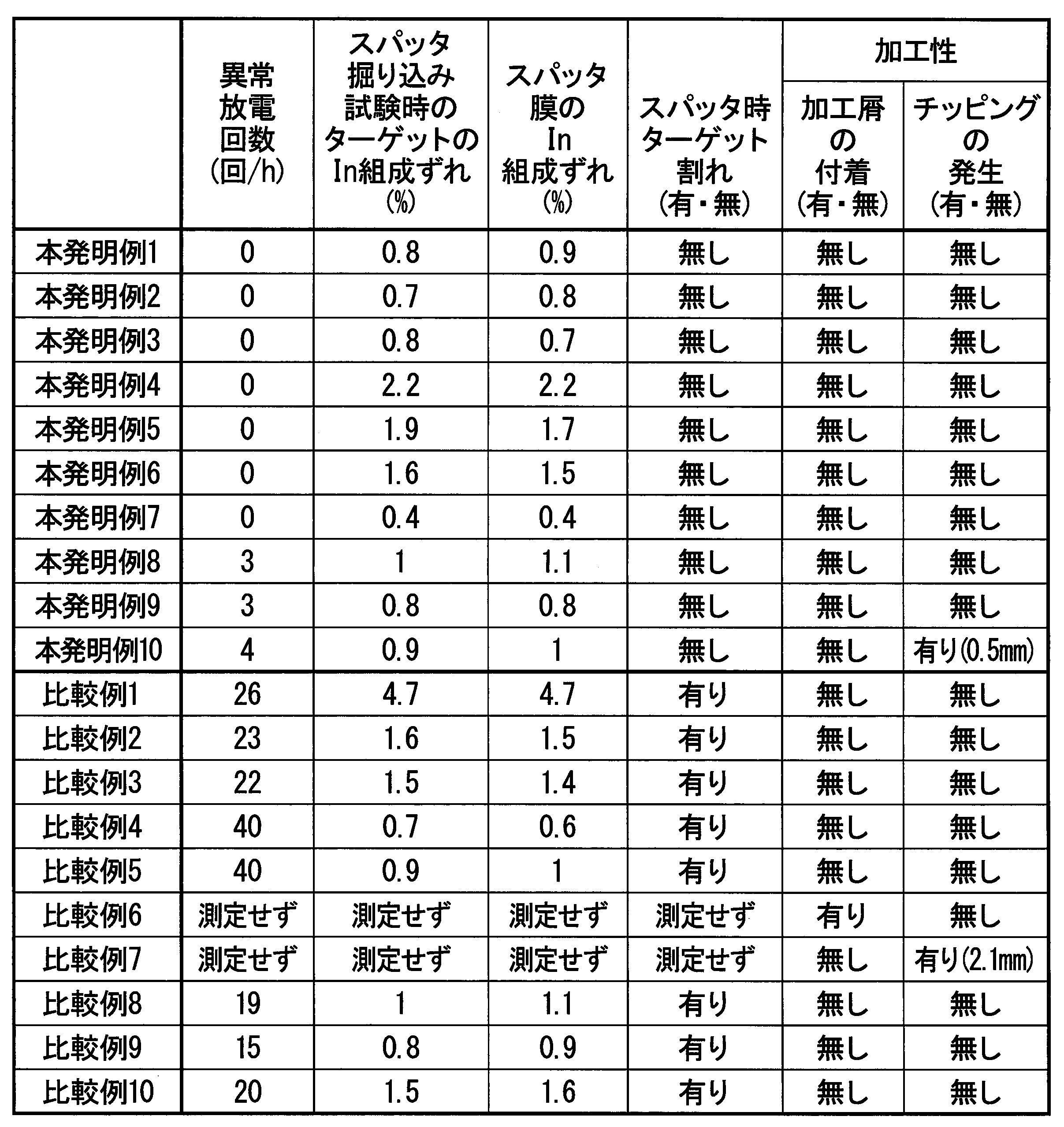
理論密度比が本発明の範囲よりも低い比較例1、2、3、8、9においては、異常放電回数が多くなった。理論密度比は本発明の範囲にあるが、密度のばらつきが本発明の範囲を超える比較例10においても異常放電回数が多くなった。
また、Inの含有量が本発明の範囲を超える比較例6は、旋盤加工時に加工屑の付着が観察され、切削加工に時間を要した。なお、比較例6は、加工屑が付着したため、異常放電回数およびスパッタ掘り込み試験時のターゲットのIn組成ずれは測定しなかった。一方、In含有量が本発明の範囲よりも少ない比較例7については、理論密度比が小さくなり、旋盤加工時に粗大なチッピングが発生した。なお、比較例7は、粗大なチッピングが発生したため、異常放電回数およびスパッタ掘り込み試験時のターゲットのIn組成ずれは測定しなかった。
Na化合物の最大粒子径が大きい比較例4においては、スパッタ時の異常放電回数が多く、高電力条件ではスパッタを継続することができなかった。また、K化合物の最大粒子径が大きい比較例5についても比較例4と同様の結果となった。
これに対して、In含有量、理論密度比および密度のばらつきが本発明の範囲にある本発明例1~10においては、旋盤加工時に加工屑の付着や粗大なチッピングの発生が認められず、加工性に優れていた。また、スパッタ時の異常放電回数も少なく、安定してスパッタ成膜が可能であることが確認された。なお、CuIn化合物相の最大粒子径が150μmを超える本発明例10では、0.5mmの微細なチッピングが発生しているが、スパッタ時の異常放電回数は4回と少ないことから、この微細なチッピングの発生は実用上問題ないレベルであると考えられる。さらに、Na化合物、K化合物の最大粒子径が本発明の範囲にある本発明例8、9においては、Na化合物、K化合物を含有しながらも異常放電の回数が少なくなった。
加工性に優れるとともに、スパッタ時の異常放電の発生を抑制することが可能なIn-Cu焼結体スパッタリングターゲット、及びこのIn-Cu焼結体スパッタリングターゲットの製造方法を提供することができる。
Claims (6)
- Inを10原子%以上90原子%以下の範囲で含有し、残部がCu及び不可避不純物からなる組成を有し、
理論密度比が97%以上であって、密度のばらつきが2%以内であることを特徴とするIn-Cu焼結体スパッタリングターゲット。 - Inの含有量のばらつきが3%以内である請求項1に記載のIn-Cu焼結体スパッタリングターゲット。
- In単体相と、CuIn化合物相とが存在し、前記In単体相は最大粒子径が1mm以下であることを特徴とする請求項1または2に記載のIn-Cu焼結体スパッタリングターゲット。
- さらにNa化合物としてNaF、NaCl、Na2S、Na2Seのうちの1種又は2種以上を含有し、このNa化合物の最大粒子径が15μm以下とされていることを特徴とする請求項1~3のいずれか一項に記載のIn-Cu焼結体スパッタリングターゲット。
- さらにK化合物としてKF、KCl、K2S、K2Seのうちの1種又は2種以上を含有し、このK化合物の最大粒子径が15μm以下とされていることを特徴とする請求項1~3のいずれか一項に記載のIn-Cu焼結体スパッタリングターゲット。
- 請求項1~5のいずれか一項に記載のIn-Cu焼結体スパッタリングターゲットの製造方法であって、
Inを10原子%以上90原子%以下の範囲で含有し、残部がCu及び不可避不純物からなる組成を有し、X線回折パターンにおけるIn単体相の(110)面に帰属されるピーク強度をI(In)、Cu単体相の(111)面に帰属されるピーク強度をI(Cu)、Cu7In3相の(-232)面に帰属されるピーク強度をI(Cu7In3)、Cu1In1相の(200)面に帰属されるピーク強度をI(Cu1In1)、Cu11In9相の(313)面に帰属されるピーク強度をI(Cu11In9)、Na化合物に起因する最大ピーク強度I(Na化合物)、K化合物相に起因する最大ピーク強度I(K化合物)とした場合に、下記の式(1)によって算出されるIn単体相の存在量が5%以上85%以下である原料粉を準備する原料粉準備工程と、
In単体相の存在量(%)=[I(In)/{I(Cu7In3)+I(Cu1In1)+I(Cu11In9)+I(In)+I(Cu)+I(Na化合物)+I(K化合物)}]×100・・・(1)
前記原料粉を90℃以上140℃以下の温度で静水圧加圧して、焼結させる焼結工程と、
を備えていることを特徴とするIn-Cu焼結体スパッタリングターゲットの製造方法。
Applications Claiming Priority (4)
| Application Number | Priority Date | Filing Date | Title |
|---|---|---|---|
| JP2017-057334 | 2017-03-23 | ||
| JP2017057334 | 2017-03-23 | ||
| JP2018-024509 | 2018-02-14 | ||
| JP2018024509A JP2018159127A (ja) | 2017-03-23 | 2018-02-14 | In−Cu焼結体スパッタリングターゲット及びIn−Cu焼結体スパッタリングターゲットの製造方法 |
Publications (1)
| Publication Number | Publication Date |
|---|---|
| WO2018174019A1 true WO2018174019A1 (ja) | 2018-09-27 |
Family
ID=63585395
Family Applications (1)
| Application Number | Title | Priority Date | Filing Date |
|---|---|---|---|
| PCT/JP2018/010847 Ceased WO2018174019A1 (ja) | 2017-03-23 | 2018-03-19 | In-Cu焼結体スパッタリングターゲット及びIn-Cu焼結体スパッタリングターゲットの製造方法 |
Country Status (1)
| Country | Link |
|---|---|
| WO (1) | WO2018174019A1 (ja) |
Citations (5)
| Publication number | Priority date | Publication date | Assignee | Title |
|---|---|---|---|---|
| KR20110109455A (ko) * | 2010-03-31 | 2011-10-06 | (주)창성 | 진공용해 분사법을 이용한 고순도 분말 제조 방법, 고순도 분말을 이용한 고순도 타겟의 제조 방법 및 고순도 타겟 |
| CN103114264A (zh) * | 2012-12-28 | 2013-05-22 | 中国神华能源股份有限公司 | 一种溅射用铜铟合金靶材及其制备方法 |
| CN103421967A (zh) * | 2012-05-17 | 2013-12-04 | 广东先导稀材股份有限公司 | 铜铟合金的制备方法 |
| JP2016513171A (ja) * | 2013-01-31 | 2016-05-12 | プランゼー エスエー | Cu−Ga−In−Naターゲット |
| JP2017082326A (ja) * | 2015-10-26 | 2017-05-18 | 三菱マテリアル株式会社 | スパッタリングターゲット及びスパッタリングターゲットの製造方法 |
-
2018
- 2018-03-19 WO PCT/JP2018/010847 patent/WO2018174019A1/ja not_active Ceased
Patent Citations (5)
| Publication number | Priority date | Publication date | Assignee | Title |
|---|---|---|---|---|
| KR20110109455A (ko) * | 2010-03-31 | 2011-10-06 | (주)창성 | 진공용해 분사법을 이용한 고순도 분말 제조 방법, 고순도 분말을 이용한 고순도 타겟의 제조 방법 및 고순도 타겟 |
| CN103421967A (zh) * | 2012-05-17 | 2013-12-04 | 广东先导稀材股份有限公司 | 铜铟合金的制备方法 |
| CN103114264A (zh) * | 2012-12-28 | 2013-05-22 | 中国神华能源股份有限公司 | 一种溅射用铜铟合金靶材及其制备方法 |
| JP2016513171A (ja) * | 2013-01-31 | 2016-05-12 | プランゼー エスエー | Cu−Ga−In−Naターゲット |
| JP2017082326A (ja) * | 2015-10-26 | 2017-05-18 | 三菱マテリアル株式会社 | スパッタリングターゲット及びスパッタリングターゲットの製造方法 |
Similar Documents
| Publication | Publication Date | Title |
|---|---|---|
| KR101249153B1 (ko) | 소결체 타겟 및 소결체의 제조 방법 | |
| JP6798852B2 (ja) | スパッタリングターゲット及びスパッタリングターゲットの製造方法 | |
| KR101337484B1 (ko) | 스퍼터링 타겟 및 그 제조방법 | |
| US20120205242A1 (en) | Cu-In-Ga-Se QUATERNARY ALLOY SPUTTERING TARGET | |
| JP6665428B2 (ja) | Cu−Ga合金スパッタリングターゲット及びその製造方法 | |
| JP2015208807A (ja) | 表面被覆窒化硼素焼結体工具 | |
| WO2019187329A1 (ja) | タングステンシリサイドターゲット部材及びその製造方法、並びにタングステンシリサイド膜の製造方法 | |
| KR101419665B1 (ko) | Cu-Ga 타겟 및 그 제조 방법 그리고 Cu-Ga 계 합금막으로 이루어지는 광흡수층 및 동 광흡수층을 이용한 CIGS 계 태양 전지 | |
| JP5153911B2 (ja) | スパッタリングターゲット及びその製造方法 | |
| JP2019044222A (ja) | In−Cu合金粉末、In−Cu合金粉末の製造方法、In−Cu合金スパッタリングターゲット及びIn−Cu合金スパッタリングターゲットの製造方法 | |
| WO2015163060A9 (ja) | 複合焼結体および表面被覆窒化硼素焼結体工具 | |
| CN104858458B (zh) | 耐异常损伤性和耐磨损性优异的表面包覆切削工具 | |
| JP2018159127A (ja) | In−Cu焼結体スパッタリングターゲット及びIn−Cu焼結体スパッタリングターゲットの製造方法 | |
| WO2018174019A1 (ja) | In-Cu焼結体スパッタリングターゲット及びIn-Cu焼結体スパッタリングターゲットの製造方法 | |
| WO2022009548A1 (ja) | 酸化モリブデンスパッタリングターゲット、および、酸化モリブデンスパッタリングターゲットの製造方法 | |
| WO2017073514A1 (ja) | スパッタリングターゲット及びスパッタリングターゲットの製造方法 | |
| WO2019202909A1 (ja) | Sn-Zn-O系酸化物焼結体とその製造方法 | |
| JP6800405B2 (ja) | 酸化物焼結体、その製造方法及びスパッタリングターゲット | |
| JP7178707B2 (ja) | MgO-TiO系スパッタリングターゲットの製造方法 | |
| US10176974B2 (en) | Tungsten sputtering target and method for producing same | |
| JP2017095781A (ja) | Cu−Ga合金スパッタリングターゲットおよびその製造方法 | |
| JP2021066957A (ja) | スパッタリングターゲット、及び、スパッタリングターゲットの製造方法 | |
| JP2021091944A (ja) | スパッタリングターゲット、及び、スパッタリングターゲットの製造方法 | |
| JP2016222971A (ja) | 金属Bi−Bi酸化物複合スパッタリングターゲット、及び、金属Bi−Bi酸化物複合スパッタリングターゲットの製造方法 | |
| TW201619402A (zh) | 由Al-Te-Cu-Zr系合金組成之濺鍍靶及其製造方法 |
Legal Events
| Date | Code | Title | Description |
|---|---|---|---|
| 121 | Ep: the epo has been informed by wipo that ep was designated in this application |
Ref document number: 18772340 Country of ref document: EP Kind code of ref document: A1 |
|
| NENP | Non-entry into the national phase |
Ref country code: DE |
|
| 122 | Ep: pct application non-entry in european phase |
Ref document number: 18772340 Country of ref document: EP Kind code of ref document: A1 |