WO2018168703A1 - 光学素子の製造装置、光学素子の製造方法および光学素子の製造装置の設定方法 - Google Patents
光学素子の製造装置、光学素子の製造方法および光学素子の製造装置の設定方法 Download PDFInfo
- Publication number
- WO2018168703A1 WO2018168703A1 PCT/JP2018/009264 JP2018009264W WO2018168703A1 WO 2018168703 A1 WO2018168703 A1 WO 2018168703A1 JP 2018009264 W JP2018009264 W JP 2018009264W WO 2018168703 A1 WO2018168703 A1 WO 2018168703A1
- Authority
- WO
- WIPO (PCT)
- Prior art keywords
- mold
- correction member
- optical element
- upper plate
- molding material
- Prior art date
- Legal status (The legal status is an assumption and is not a legal conclusion. Google has not performed a legal analysis and makes no representation as to the accuracy of the status listed.)
- Ceased
Links
- 0 CCC(CCC1)C1*(CC)=C Chemical compound CCC(CCC1)C1*(CC)=C 0.000 description 1
- OJMKUNLMAJOBBX-UHFFFAOYSA-N CCCCCCC(CCC)CC(CC)(CC(C)C(C)CC=C)CC1CCCCC1 Chemical compound CCCCCCC(CCC)CC(CC)(CC(C)C(C)CC=C)CC1CCCCC1 OJMKUNLMAJOBBX-UHFFFAOYSA-N 0.000 description 1
Images



Classifications
-
- C—CHEMISTRY; METALLURGY
- C03—GLASS; MINERAL OR SLAG WOOL
- C03B—MANUFACTURE, SHAPING, OR SUPPLEMENTARY PROCESSES
- C03B11/00—Pressing molten glass or performed glass reheated to equivalent low viscosity without blowing
-
- G—PHYSICS
- G02—OPTICS
- G02B—OPTICAL ELEMENTS, SYSTEMS OR APPARATUS
- G02B3/00—Simple or compound lenses
Definitions
- the present invention relates to an optical element manufacturing apparatus, an optical element manufacturing method, and an optical element manufacturing apparatus setting method.
- a molding die is arranged between flat plates that are arranged to face each other and at least one of which is movable, and the molding material is heated, pressed, and cooled by the die. By doing so, an optical element is manufactured.
- Patent Document 1 proposes a manufacturing apparatus provided with an adjustment mechanism that adjusts the parallelism between the plates.
- the present invention has been made in view of the above, and it is possible to set an optical element manufacturing apparatus, an optical element manufacturing method, and an optical element manufacturing apparatus having high decentering accuracy without adjusting the parallelism between the plates. It aims to provide a method.
- an optical element manufacturing apparatus is an optical element manufacturing apparatus that molds an optical element by pressing and deforming a molding material disposed in a mold. And an upper plate and a lower plate each having a pressing surface for applying a pressing force to an upper die and a lower die constituting the mold, and the upper plate has a relative relationship between the pressing surfaces of the upper plate and the lower plate. And a connecting member that can be mounted on the press surface.
- the optical element manufacturing apparatus includes the correction member in the above invention, and the correction member has an inclination transferred to the correction member so that the inclination between the press surfaces coincides.
- the connecting member is attached to the press surface of the upper plate.
- the optical element manufacturing apparatus is characterized in that, in the above invention, the correction member is made of a material that does not deform in a manufacturing temperature range of the molding material.
- the method of manufacturing an optical element according to the present invention applies a pressing force to the mold by the press surfaces of the upper plate and the lower plate, and enters the mold.
- the upper plate and the lower plate are disposed in a correction member die composed of an upper die and a lower die, and a pressing force is applied to the correction member die by the upper plate and the lower plate.
- the molding material is arranged in the mold composed of an upper mold and a lower mold having a transfer surface for creating a desired optical functional surface, and the upper plate and the lower plate are used to pass the correction member through the correction member. And a manufacturing process of applying a pressing force to the mold and transferring the optical functional surface to the molding material.
- a method for setting an optical element manufacturing apparatus applies a pressing force to a mold by the press surfaces of an upper plate and a lower plate, and A method for setting a manufacturing apparatus for molding an optical element from a molding material arranged in a mold, wherein each of the molding materials for a correction member made of a material that does not deform in the manufacturing temperature zone of the molding material has a planar transfer surface.
- correction member mold composed of an upper mold and a lower mold, and a pressing force is applied to the correction member mold by the upper plate and the lower plate, so that the upper plate and the lower plate After forming a correction member that has transferred the relative inclination between the press surfaces, the correction member is mounted on the press surface of the upper plate.
- the relative inclination between the press surfaces can be offset by pressing the molding material via the correction member that has transferred the relative inclination between the press surfaces in the upper plate and the lower plate. Therefore, it is possible to manufacture an optical element having high eccentricity accuracy without adjusting the parallelism between the plates.
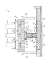
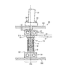
- FIG. 1 is a cross-sectional view showing a configuration of an optical element manufacturing apparatus according to an embodiment of the present invention.
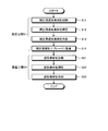
- FIG. 2 is a flowchart showing a method for manufacturing an optical element according to an embodiment of the present invention.
- FIG. 3 is a cross-sectional view for explaining a setting method of the optical element manufacturing apparatus according to the embodiment of the present invention.
- FIG. 4 is a cross-sectional view for explaining an optical element manufacturing apparatus and an optical element manufacturing method using the same according to an embodiment of the present invention.
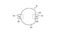
- FIG. 5 is a plan view showing an example of a correction member in the optical element manufacturing apparatus according to the embodiment of the present invention.
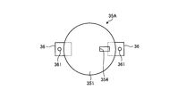
- FIG. 6 is a plan view showing another example of the correction member in the optical element manufacturing apparatus according to the embodiment of the present invention.
- FIG. 7 is a cross-sectional view showing a configuration of a modification of the optical element manufacturing apparatus according to the embodiment of the present invention.
- FIG. 8 is a cross-sectional view showing a conventional optical element manufacturing apparatus and
- the optical element manufacturing apparatus presses and deforms a molding material (glass material) placed in a mold to mold an optical element (glass lens). Yes, as shown in FIG. 1, a molding apparatus 1 and a mold set (mold) 10 are provided.
- the molding apparatus 1 is a circulation type molding apparatus that continuously circulates the mold set 10 conveyed into the molding chamber 30 and molds optical elements.
- the molding apparatus 1 includes a molding chamber 30 including a heating stage 30a, a press stage 30b, and a cooling stage 30c, and a transport arm (not shown) that transports the mold set 10 into the molding chamber 30.
- the molding chamber 30 includes a molding chamber upper plate 301, a molding chamber lower plate 302, an inlet shutter 303 that opens and closes when the mold set 10 is introduced into the molding chamber 30, and when the mold set 10 is discharged from the molding chamber 30. And an exit shutter 304 that opens and closes.
- the molding chamber 30 is filled with an inert gas (for example, nitrogen gas).
- Each stage (heating stage 30a, press stage 30b and cooling stage 30c) of the molding chamber 30 is provided with an upper plate 31 on the upper side and a lower plate 32 on the lower side.
- the upper plate 31 and the lower plate 32 of each stage have press surfaces 311 and 321 for applying a pressing force to the upper die 11 and the lower die 12 constituting the die set 10.
- the upper plate 31 and the lower plate 32 of each stage are each provided with a heater, and the molding material M in the mold set 10 is heated or cooled via the heater.
- the upper plate 31 of each stage is provided with a drive unit 33 on the upper side, and the drive unit 33 can perform vertical movement and press on the mold set 10.
- the driving unit 33 is fixed to the upper plate 301 of the molding chamber by a fixing screw 34.
- the upper plate 31 of the press stage 30b includes an attachment (connecting member) 36 that can be removed by screwing and that can attach (lock) the correction member 35 to the press surface 311.
- the correction member 35 has a relative inclination between the press surfaces 311 and 321 of the upper plate 31 and the lower plate 32 transferred thereto, and is attached to the press surface 311 by an attachment 36.
- the attachment 36 has an L-shaped cross section.
- the mold set 10 includes an upper mold 11, a lower mold 12, and a sleeve 13.
- the upper mold 11 and the lower mold 12 are each formed in a stepped cylindrical shape, and are arranged so that the transfer surfaces 11a and 12a face each other.
- the transfer surface 11a of the upper mold 11 is for creating a concave optical functional surface in the optical element. That is, the upper mold 11 has a spherical convex portion formed on the end surface facing the lower mold 12, and the convex portion constitutes the transfer surface 11a.
- the transfer surface 12a of the lower mold 12 is for creating a convex optical functional surface on the optical element. That is, the lower mold 12 has a spherical recess formed on the end surface facing the upper mold 11, and the recess constitutes the transfer surface 12a.
- the sleeve 13 is for supporting the upper die 11 and the lower die 12 and positioning them.
- the sleeve 13 is formed in a cylindrical shape and is disposed around the upper mold 11 and the lower mold 12.
- the press surface 311 of the upper plate 31 and the press surface 321 of the lower plate 32 have a relative inclination ⁇ that is not 0 due to various processing errors, mounting errors, and the like. .
- This inclination ⁇ is affected by the thermal expansion and thermal deformation of the members constituting the molding apparatus 1 or the bending due to the pressing force of the molding chamber 30 fixing the press stage 30b when the optical element is actually molded. Change in response. Note that the inclination ⁇ is actually assumed to be a minute value of about 1/60 degrees, for example, and FIG. 8 exaggerates the value of the inclination ⁇ for convenience of explanation (FIG. 3 to be described later). The inclination ⁇ shown in FIGS. 4 and 7 is also the same).
- the inclination ⁇ is also transferred to the optical element after molding.
- the gap between the upper mold 11 and the lower mold 12 and the sleeve 13 is sufficiently large, the inclination ⁇ is directly transferred to the optical element after molding.
- the inclination ⁇ is regulated by the sleeve 13, so that the upper mold 11 and the lower mold 12 are the optical elements after molding.
- the maximum possible inclination ( ⁇ inclination ⁇ ) is transferred.
- the conventional molding apparatus has a problem that an inclination that is not at least 0 is transferred to the optical element after molding.
- the correction member 35 to which the relative inclination ⁇ between the upper and lower press surfaces 311 and 321 is previously transferred is manufactured, and the gap between the upper plate 31 and the mold set 10 is manufactured. Further, the inclination ⁇ is offset by pressing the correction member 35 with the correction member 35 interposed therebetween.
- the manufacturing method of the optical element according to the present embodiment includes a manufacturing device setting step (manufacturing device setting method) S1 and an optical element manufacturing step S2.
- a correction member molding material Mc made of a material that does not deform in the manufacturing temperature zone of the molding material M is placed in a correction member mold set (correction member mold) 40.
- the correction member 35 is formed by applying the pressing force to the correction member mold set 40 by the upper plate 31 and the lower plate 32 and then mounting the correction member 35 on the upper plate 31.
- a glass material “L-LAH53” is used as the correction member molding material Mc.
- the correction member molding material Mc is not limited to the L-LAH 53, but is composed of a material that does not deform in the manufacturing temperature range of the molding material M, as will be described later.
- the shape of the correction member molding material Mc is, for example, a cylindrical shape having a thickness of 5 mm, and the upper surface and the lower surface are polished.
- the correction member mold set 40 includes an upper mold 41, a lower mold 42, and a sleeve 43.
- Each of the upper mold 41 and the lower mold 42 has planar transfer surfaces 41a and 42a that are plane processed with high precision, and transfers the planar upper and lower surfaces to the correction member molding material Mc.
- a sufficiently large gap of, for example, about 0.1 mm is formed between the upper die 41 and the lower die 42 and the sleeve 43, and the relative inclination ⁇ between the upper and lower press surfaces 311 and 321 is set. It is configured not to regulate.
- the configurations other than the correction member mold set 40 and the correction member molding material Mc are the same as those in the optical element manufacturing step S2 described later, and the inclination ⁇ can be reproduced. Set the environment.
- the correction member molding material Mc is arranged in the correction member mold set 40, and the correction member mold set 40 is conveyed to the heating stage 30a of the molding chamber 30 by a conveyance arm (not shown). .
- the correction member mold set 40 is heated to 620 ° C. (see step S11 in FIG. 2), and the correction member molding material Mc is softened.
- the correction member mold set 40 is transported to the press stage 30b by a transport arm (not shown), and a pressure of 3 MPa is applied to the upper plate 31 by the drive unit 33 while maintaining 620 ° C. It gives and presses (refer step S12 of FIG. 2). Accordingly, the correction member molding material Mc is gradually deformed, and when the thickness reaches, for example, 4 mm, the upper plate 31 is retracted upward, and the pressing is finished.
- the correction member mold set 40 is transferred to the cooling stage 30c by a transfer arm (not shown), and the correction member mold set 40 is cooled to 100 ° C. (see step S13 in FIG. 2).
- the set 40 is discharged from the molding chamber 30.
- the correction member 35 is mounted on the upper plate 31 by the attachment 36 (see step S14 in FIG. 2). Specifically, the correction member 35 is attached to the press surface 311 of the upper plate 31 by the attachment 36 so that the inclination ⁇ transferred to the correction member 35 coincides with the inclination ⁇ between the upper and lower press surfaces 311 and 321. Installed.
- the correction member 35 when the correction member 35 is mounted, it is necessary to mount it with high accuracy with respect to the rotation direction around the optical axis (see the dashed line in FIG. 4). Accordingly, as shown in FIG. 5, for example, the correction member 35 is provided with a flat portion 353 for restricting the rotation direction in at least one direction and the pressing step of the correction member molding material Mc described above (see FIG. 3). ) And the upper plate 31 is mounted on the press surface 311 of the upper plate 31 while maintaining the positional relationship in the rotational direction around the optical axis.
- Reference numeral 361 denotes a fixing screw (not shown) for fixing the attachment 36 to the press surface 311 of the upper plate 31. ) Is a screw hole to be inserted.
- the flat surface portion 353 of the correction member 35 as shown in the figure is, for example, a restriction member having a shape formed by an arc and a straight line at a position corresponding to the flat surface portion 353 in the pressing process of the correction member molding material Mc described above. It can be formed by pressing in the arranged state.
- a marking 354 made of a linear groove or the like is provided on the upper surface 351 of the cylindrical correction member 35A, and the marking 354 and the press surface 311 of the upper plate 31 are provided in advance.
- the correction member 35A may be attached to the press surface 311 by the attachment 36 so that the shape marking (for example, a linear mark) matches.
- the correction member 35A is held while maintaining the positional relationship in the rotation direction around the optical axis with the upper plate 31 in the pressing step of the correction member molding material Mc (see FIG. 3).
- the marking 354 shown in the figure is pressed by using the upper die 41 provided with a linear protrusion corresponding to the marking 354 on the transfer surface in the pressing step of the correction member molding material Mc described above, for example. Can be formed.
- the molding material M is arranged in the mold set 10, and a pressing force is applied to the mold set 10 via the correction member 35 by the upper plate 31 and the lower plate 32. In this process, the optical functional surface is transferred to the molding material M.
- a glass material “S-FPL51” is used as the molding material M.
- the shape of the molding material M is a ball shape (spherical shape), and the surface is polished.
- the relative inclination ⁇ between the upper and lower press surfaces 311 and 321 has the same inclination ⁇ . It is offset by the correction member 35. Accordingly, the relative inclination between the lower surface 352 of the correction member 35 and the press surface 321 of the lower plate 32 becomes zero.
- a gap is formed between the lower surface 352 of the correction member 35 and the attachment 36 on the right side of the paper.
- the actual inclination ⁇ is a minute value of about 1/60 degrees. Therefore, the gap described above is actually very small.
- the correction member 35 is sandwiched between the upper plate 31 and the upper mold 11 without a gap, so the presence or absence of the gap does not cause a problem during molding. .
- the molding material M is placed in the mold set 10, and the mold set 10 is transported to the heating stage 30 a of the molding chamber 30 by a transport arm (not shown). And in the heating stage 30a, the type
- the mold set 10 is transported to the press stage 30 b by a transport arm (not shown), and a pressing force of 3 MPa is applied to the upper plate 31 by the drive unit 33 while maintaining 500 ° C. Pressing is performed (see step S22 in FIG. 2).
- the pressing force by the upper plate 31 acts on the upper mold 11 via the correction member 35.
- the correction member 35 is not deformed during pressing, and it is possible to apply a pressing force to the upper die 11 while maintaining a state in which the relative inclination ⁇ between the upper and lower press surfaces 311 and 321 is offset. It becomes.
- the pressing step the molding material M is gradually deformed by such a pressing force, and when the desired thickness is reached, the upper plate 31 is retracted upward and the pressing ends.
- the mold set 10 is transported to the cooling stage 30c by a transport arm (not shown), the mold set 10 is cooled to 100 ° C. (see step S23 in FIG. 2), and the cooled mold set 10 is discharged from the molding chamber 30. .
- a transport arm not shown
- the mold set 10 is cooled to 100 ° C. (see step S23 in FIG. 2)
- the cooled mold set 10 is discharged from the molding chamber 30. .
- the press surfaces 311 and 321 of the upper plate 31 and the lower plate 32 are relatively relative to each other.
- the relative inclination between the press surfaces 311 and 321 can be canceled out, so that it is high without adjusting the parallelism between the plates. It becomes possible to manufacture an optical element having decentration accuracy.
- the molding apparatus according to the modified example does not include the attachment 36, and a suction portion 37 that performs intake is provided inside the upper plate 31A.
- the suction unit 37 is connected to a suction device (not shown).
- the correction member 35 is attracted to and held on the press surface 311 of the upper plate 31A by the suction portion 37.
- the correction member 35 is attracted to the press surface 311 while pressing the correction member 35 against the press surface 311 using a jig for adjusting the rotational direction.
- optical element manufacturing apparatus the optical element manufacturing method, and the optical element manufacturing apparatus setting method according to the present invention have been specifically described above by the embodiments for carrying out the invention. It is not limited to the description, but should be interpreted broadly based on the description of the claims. Needless to say, various changes and modifications based on these descriptions are also included in the spirit of the present invention.
- the present invention may be applied to a mold-fixing molding apparatus.
- the correction member 35 is attached only to the upper plate 31 of the press stage 30b. However, the correction member 35 is attached to the upper plate 31 of the heating stage 30a or the cooling stage 30c as necessary. You may wear it.
Landscapes
- Physics & Mathematics (AREA)
- Engineering & Computer Science (AREA)
- Chemical & Material Sciences (AREA)
- General Physics & Mathematics (AREA)
- Optics & Photonics (AREA)
- Manufacturing & Machinery (AREA)
- Materials Engineering (AREA)
- Organic Chemistry (AREA)
- Casting Or Compression Moulding Of Plastics Or The Like (AREA)
Abstract
光学素子の製造装置は、型セット10内に配置した成形素材Mを押圧変形して光学素子を成形するものであり、型セット10を構成する上型11および下型12に押圧力を付与するプレス面311,321をそれぞれ有する上部プレート31および下部プレート32を備え、上部プレート31が、上部プレート31および下部プレート32におけるプレス面311,321同士の相対的な傾きを転写した補正部材35を、プレス面311に装着可能なアタッチメント36を備えている。
Description
本発明は、光学素子の製造装置、光学素子の製造方法および光学素子の製造装置の設定方法に関する。
一般に、光学素子の製造装置では、互いに対向して配置され、少なくとも一方が可動する平板状のプレートの間に成形用の金型を配置し、当該金型によって成形素材を加熱、押圧成形および冷却することにより、光学素子を製造する。
このような方法によって製造される光学素子は、金型を押圧する2つのプレートのプレス面が互いに平行になっていないと、製造された光学素子の偏心精度が悪化するという問題がある。このような問題に対して、例えば特許文献1では、プレート間の平行度を調整する調整機構を設けた製造装置が提案されている。
特許文献1で提案された調整機構を用いたプレート間の平行度の調整は、きわめて精密な調整作業であることや、作業の安全性等を考慮すると、製造装置に熱や圧力がかからない状態で行う必要がある。しかしながら、実際に光学素子を製造する加熱および押圧成形の工程では、製造装置の熱変形やプレートの押圧力による製造装置の撓み等の影響を必然的に受けてしまうため、仮に調整機構によって平行度を調整したとしても、製造中に平行度が変化してしまう。
また、特許文献1で提案されたような調整機構では、当該調整機構を製造装置に取り付けるネジの締め込み具合等にばらつきがあることが通常であるため、このような調整機構によってプレート間の平行度を正確に調整するには困難を伴う。しかも、平行度の調整は、光学素子の偏心精度を向上させようとすればするほど精密さが必要となり、その調整が困難となる。また、そもそもプレート間の平行度を調整しようとすると複雑な調整機構が必要となり、コストも増加する。
本発明は、上記に鑑みてなされたものであって、プレート間の平行度を調整することなく、高い偏心精度を持つ光学素子の製造装置、光学素子の製造方法および光学素子の製造装置の設定方法を提供することを目的とする。
上述した課題を解決し、目的を達成するために、本発明に係る光学素子の製造装置は、金型内に配置した成形素材を押圧変形して光学素子を成形する光学素子の製造装置であって、前記金型を構成する上型および下型に押圧力を付与するプレス面をそれぞれ有する上部プレートおよび下部プレートを備え、前記上部プレートは、前記上部プレートおよび前記下部プレートにおけるプレス面同士の相対的な傾きを転写した補正部材を、前記プレス面に装着可能な接続部材を備えることを特徴とする。
また、本発明に係る光学素子の製造装置は、上記発明において、前記補正部材を備え、前記補正部材は、前記補正部材に転写された傾きが、前記プレス面同士の傾きと一致するように、前記接続部材によって前記上部プレートのプレス面に装着されていることを特徴とする。
また、本発明に係る光学素子の製造装置は、上記発明において、前記補正部材は、前記成形素材の製造温度帯では変形しない材料からなることを特徴とする。
上述した課題を解決し、目的を達成するために、本発明に係る光学素子の製造方法は、上部プレートおよび下部プレートのそれぞれのプレス面により金型に押圧力を付与し、前記金型内に配置した成形素材から光学素子を成形する製造装置を用いた光学素子の製造方法であって、前記成形素材の製造温度帯では変形しない材料からなる補正部材用成形素材を、それぞれ平面状の転写面を有する上型および下型から構成された補正部材用金型内に配置し、前記上部プレートおよび前記下部プレートによって前記補正部材用金型に押圧力を付与することにより、前記上部プレートおよび前記下部プレートにおけるプレス面同士の相対的な傾きを転写した補正部材を成形した後、前記上部プレートのプレス面に前記補正部材を装着する設定工程と、所望の光学機能面を創生する転写面を有する上型および下型から構成された前記金型内に前記成形素材を配置し、前記上部プレートおよび前記下部プレートによって、前記補正部材を介して前記金型に押圧力を付与し、前記成形素材に前記光学機能面を転写する製造工程と、を含むことを特徴とする。
上述した課題を解決し、目的を達成するために、本発明に係る光学素子の製造装置の設定方法は、上部プレートおよび下部プレートのそれぞれのプレス面により金型に押圧力を付与し、前記金型内に配置した成形素材から光学素子を成形する製造装置の設定方法であって、前記成形素材の製造温度帯では変形しない材料からなる補正部材用成形素材を、それぞれ平面状の転写面を有する上型および下型から構成された補正部材用金型内に配置し、前記上部プレートおよび前記下部プレートによって前記補正部材用金型に押圧力を付与することにより、前記上部プレートおよび前記下部プレートにおけるプレス面同士の相対的な傾きを転写した補正部材を成形した後、前記上部プレートのプレス面に前記補正部材を装着することを特徴とする。
本発明によれば、上部プレートおよび下部プレートにおけるプレス面同士の相対的な傾きを転写した補正部材を介して成形素材を押圧することにより、プレス面同士の相対的な傾きを相殺することができるため、プレート間の平行度を調整することなく、高い偏心精度を持つ光学素子を製造することが可能となる。
以下、本発明に係る光学素子の製造装置、光学素子の製造方法および光学素子の製造装置の設定方法の実施の形態について、図面を参照しながら説明する。なお、本発明は以下の実施の形態に限定されるものではなく、以下の実施の形態における構成要素には、当業者が置換可能かつ容易なもの、あるいは実質的に同一のものも含まれる。
[光学素子の製造装置]
本実施の形態に係る光学素子の製造装置(以下、「製造装置」という)は、金型内に配置した成形素材(ガラス素材)を押圧変形して光学素子(ガラスレンズ)を成形するものであり、図1に示すように、成形装置1と、型セット(金型)10と、を備えている。
本実施の形態に係る光学素子の製造装置(以下、「製造装置」という)は、金型内に配置した成形素材(ガラス素材)を押圧変形して光学素子(ガラスレンズ)を成形するものであり、図1に示すように、成形装置1と、型セット(金型)10と、を備えている。
成形装置1は、成形室30内に搬送された型セット10を連続的に循環させて光学素子の成形を行う循環式の成形装置である。成形装置1は、加熱ステージ30a、プレスステージ30bおよび冷却ステージ30cを備える成形室30と、成形室30内に型セット10を搬送する図示しない搬送アームと、を備えている。
成形室30は、成形室上板301と、成形室下板302と、型セット10を成形室30に導入する際に開閉する入口シャッター303と、型セット10を成形室30から排出する際に開閉する出口シャッター304と、を備えている。また、成形室30内は、不活性ガス(例えば窒素ガス)で満たされている。
成形室30の各ステージ(加熱ステージ30a、プレスステージ30bおよび冷却ステージ30c)は、上側に上部プレート31が、下側に下部プレート32が設けられている。各ステージの上部プレート31および下部プレート32は、型セット10を構成する上型11および下型12に押圧力を付与するプレス面311,321を有している。また、各ステージの上部プレート31および下部プレート32は、内部にそれぞれヒータを備えており、当該ヒータを介して型セット10内の成形素材Mを加熱または冷却する。また、各ステージの上部プレート31は、上側に駆動部33が設けられており、当該駆動部33により、上下動作と型セット10への押圧が可能となっている。
駆動部33は、固定ネジ34によって成形室上板301に固定されている。また、プレスステージ30bの上部プレート31は、ネジ止めにより取り外し可能であり、かつ補正部材35をプレス面311に装着(係止)可能なアタッチメント(接続部材)36を備えている。補正部材35は、後記するように、上部プレート31および下部プレート32におけるプレス面311,321同士の相対的な傾きが転写されており、アタッチメント36によってプレス面311に装着されている。なお、アタッチメント36は、断面がL字状に形成されている。
型セット10は、上型11と、下型12と、スリーブ13と、を備えている。上型11および下型12は、それぞれ段付きの円柱形状に形成されており、それぞれの転写面11a,12aが対向するように配置されている。
上型11の転写面11aは、光学素子に凹形状の光学機能面を創生するためのものである。すなわち、上型11は、下型12と対向する端面に球面状の凸部が形成されており、その凸部が転写面11aを構成している。
下型12の転写面12aは、光学素子に凸形状の光学機能面を創生するためのものである。すなわち、下型12は、上型11と対向する端面に、球面状の凹部が形成されており、その凹部が転写面12aを構成している。
スリーブ13は、上型11および下型12を支持し、かつ両者の位置決めを行うためのものである。スリーブ13は、円筒状に形成されており、上型11および下型12の周囲に配置されている。
ここで、本発明が解決すべき課題である上部プレート31と下部プレート32との間の傾きについて、図8を参照しながら説明する。同図に示すように上部プレート31のプレス面311と、下部プレート32のプレス面321とは、様々な加工誤差や取付誤差等に起因して、0ではない相対的な傾きαを持っている。
この傾きαは、実際に光学素子を成形する際には、成形装置1を構成する部材の熱膨張や熱変形、あるいはプレスステージ30bを固定している成形室30の押圧力による撓みの影響を受けて変化する。なお、傾きαは、実際には例えば1/60度程度の微小な値を想定しており、図8では説明の便宜上、この傾きαの値を誇張して図示している(後記する図3、図4および図7に示した傾きαも同様)。
図8に示すように、上下のプレス面311,321同士に相対的な傾きαを持った状態で成形素材Mを押圧すると、成形後の光学素子にも傾きαが転写される。なお、同図に示すように、上型11および下型12と、スリーブ13との間の隙間が十分大きい場合、成形後の光学素子には、傾きαがそのまま転写される。一方、例えば上型11および下型12と、スリーブ13との間の隙間が小さい場合、傾きαがスリーブ13によって規制されるため、成形後の光学素子には、上型11および下型12が取り得る最大の傾き(<傾きα)が転写される。このように、従来の成形装置では、少なくとも0ではない傾きが成形後の光学素子に転写されるという問題がある。
そこで、本実施の形態では、図1に示すように、予め上下のプレス面311,321同士の相対的な傾きαを転写した補正部材35を製作し、上部プレート31と型セット10との間にこの補正部材35を挟んだ状態で押圧することにより、前記した傾きαを相殺する構成としている。
[光学素子の製造方法]
以下、製造装置を利用した本実施の形態に係る光学素子の製造方法について、図1~図7を参照しながら説明する。本実施の形態に係る光学素子の製造方法は、図2に示すように、製造装置の設定工程(製造装置の設定方法)S1と、光学素子の製造工程S2と、を行う。
以下、製造装置を利用した本実施の形態に係る光学素子の製造方法について、図1~図7を参照しながら説明する。本実施の形態に係る光学素子の製造方法は、図2に示すように、製造装置の設定工程(製造装置の設定方法)S1と、光学素子の製造工程S2と、を行う。
製造装置の設定工程S1は、図3に示すように、成形素材Mの製造温度帯では変形しない材料からなる補正部材用成形素材Mcを補正部材用型セット(補正部材用金型)40内に配置し、上部プレート31および下部プレート32によって補正部材用型セット40に押圧力を付与することにより補正部材35を成形した後、上部プレート31に補正部材35を装着する工程である。
製造装置の設定工程S1では、補正部材用成形素材Mcとして、例えばガラス素材「L-LAH53」を使用する。L-LAH53は、屈服点At=607℃、転移点Tg=574℃の材料であり、607℃付近では成形しやすく、574℃以下では変形しない性質を有している。なお、補正部材用成形素材Mcは、L-LAH53に限定されないが、後記するように、成形素材Mの製造温度帯では変形しない素材で構成される。また、補正部材用成形素材Mcの形状は、例えば厚み5mmの円筒形状であり、上面および下面は研磨されている。
補正部材用型セット40は、上型41と、下型42と、スリーブ43と、を備えている。上型41および下型42は、それぞれ精度良く平面加工された平面状の転写面41a,42aを有しており、補正部材用成形素材Mcに平面状の上面および下面を転写する。なお、上型41および下型42と、スリーブ43との間には、例えば0.1mm程度の十分に大きい隙間が形成されており、上下のプレス面311,321同士の相対的な傾きαを規制しないように構成されている。また、製造装置の設定工程S1において、補正部材用型セット40および補正部材用成形素材Mc以外の構成は、全て後記する光学素子の製造工程S2と同じものを用い、傾きαを再現できるような環境に設定する。
(加熱工程)
製造装置の設定工程S1では、まず補正部材用型セット40内に補正部材用成形素材Mcを配置し、図示しない搬送アームによって当該補正部材用型セット40を成形室30の加熱ステージ30aに搬送する。そして、加熱ステージ30aにおいて、補正部材用型セット40を620℃まで加熱し(図2のステップS11参照)、補正部材用成形素材Mcを軟化させる。
製造装置の設定工程S1では、まず補正部材用型セット40内に補正部材用成形素材Mcを配置し、図示しない搬送アームによって当該補正部材用型セット40を成形室30の加熱ステージ30aに搬送する。そして、加熱ステージ30aにおいて、補正部材用型セット40を620℃まで加熱し(図2のステップS11参照)、補正部材用成形素材Mcを軟化させる。
(押圧工程)
続いて、図3に示すように、図示しない搬送アームによって補正部材用型セット40をプレスステージ30bに搬送し、620℃を維持した状態で、駆動部33によって上部プレート31に3MPaの押圧力を付与して押圧を行う(図2のステップS12参照)。これにより、補正部材用成形素材Mcを徐々に変形させ、厚さが例えば4mmとなった時点で上部プレート31を上方に退避させて押圧を終了する。
続いて、図3に示すように、図示しない搬送アームによって補正部材用型セット40をプレスステージ30bに搬送し、620℃を維持した状態で、駆動部33によって上部プレート31に3MPaの押圧力を付与して押圧を行う(図2のステップS12参照)。これにより、補正部材用成形素材Mcを徐々に変形させ、厚さが例えば4mmとなった時点で上部プレート31を上方に退避させて押圧を終了する。
(冷却工程)
続いて、図示しない搬送アームによって補正部材用型セット40を冷却ステージ30cに搬送し、補正部材用型セット40を100℃まで冷却し(図2のステップS13参照)、冷却後の補正部材用型セット40を成形室30から排出する。以上の手順により、上下のプレス面311,321同士の相対的な傾きαが転写された補正部材35を成形する。
続いて、図示しない搬送アームによって補正部材用型セット40を冷却ステージ30cに搬送し、補正部材用型セット40を100℃まで冷却し(図2のステップS13参照)、冷却後の補正部材用型セット40を成形室30から排出する。以上の手順により、上下のプレス面311,321同士の相対的な傾きαが転写された補正部材35を成形する。
(装着工程)
そして最後に、図4に示すように、アタッチメント36により、上部プレート31に補正部材35を装着する(図2のステップS14参照)。補正部材35は、具体的には、当該補正部材35に転写された傾きαが、上下のプレス面311,321同士の傾きαと一致するように、アタッチメント36によって上部プレート31のプレス面311に装着される。
そして最後に、図4に示すように、アタッチメント36により、上部プレート31に補正部材35を装着する(図2のステップS14参照)。補正部材35は、具体的には、当該補正部材35に転写された傾きαが、上下のプレス面311,321同士の傾きαと一致するように、アタッチメント36によって上部プレート31のプレス面311に装着される。
また、補正部材35の装着する際は、光軸(図4の一点鎖線参照)を中心とした回転方向に対して、精度良く装着する必要がある。従って、補正部材35には、例えば図5に示すように、回転方向を規制するための平面部353を少なくとも一方向以上に設け、かつ前記した補正部材用成形素材Mcの押圧工程(図3参照)における上部プレート31との間の光軸を中心とした回転方向の位置関係を保持しつつ、上部プレート31のプレス面311に装着する。
なお、図5は、図4における補正部材35およびアタッチメント36を上から見た状態を示しており、符号361は、アタッチメント36を上部プレート31のプレス面311に固定する際の固定ネジ(図示省略)が挿入されるネジ孔である。また、同図に示すような補正部材35の平面部353は、例えば前記した補正部材用成形素材Mcの押圧工程において、平面部353に相当する位置に、円弧および直線からなる形状の規制部材を配置した状態で押圧を行うことにより、形成することが可能である。
またその他に、例えば図6に示すように、円筒形状の補正部材35Aの上面351に直線状の溝等からなるマーキング354を設け、そのマーキング354と上部プレート31のプレス面311に予め設けた同形状のマーキング(例えば直線状の印)とが一致するように、アタッチメント36によって補正部材35Aをプレス面311に装着してもよい。なお、この場合も、前記した補正部材用成形素材Mcの押圧工程(図3参照)における上部プレート31との間の光軸を中心とした回転方向の位置関係を保持しつつ、補正部材35Aをプレス面311に装着する。なお、同図に示すマーキング354は、例えば前記した補正部材用成形素材Mcの押圧工程において、マーキング354に対応する直線状の突起部が転写面に設けられた上型41を用いて押圧することにより、形成することが可能である。
光学素子の製造工程S2は、図4に示すように、型セット10内に成形素材Mを配置し、上部プレート31および下部プレート32によって、補正部材35を介して型セット10に押圧力を付与し、成形素材Mに光学機能面を転写する工程である。
光学素子の製造工程S2では、成形素材Mとして、例えばガラス素材「S-FPL51」を使用する。S-FPL51は、屈服点At=489℃、転移点Tg=458℃の材料であり、489℃付近では成形しやすく、458℃以下では変形しない性質を有している。また、成形素材Mの形状は、ボール形状(球形状)であり、表面は研磨されている。
光学素子の製造工程S2では、前記したように、補正部材35が上部プレート31に装着されたプレスステージ30bにおいて、上下のプレス面311,321同士の相対的な傾きαが、同じ傾きαを有する補正部材35によって相殺されている。従って、補正部材35の下面352と下部プレート32のプレス面321との間の相対的な傾きは0になる。なお、図4では、補正部材35の下面352と、紙面右側のアタッチメント36との間に隙間が形成されているが、前記したように、実際の傾きαは1/60度程度の微小な値であるため、前記した隙間も実際には非常に小さなものである。さらに、後記する成形素材Mの押圧工程では、上部プレート31と上型11とによって補正部材35が隙間なく挟まれている状態となるため、前記した隙間の有無は成形の際の問題とはならない。
(加熱工程)
光学素子の製造工程S2では、まず型セット10内に成形素材Mを配置し、図示しない搬送アームによって当該型セット10を成形室30の加熱ステージ30aに搬送する。そして、加熱ステージ30aにおいて、型セット10を500℃まで加熱し(図2のステップS21参照)、成形素材Mを軟化させる。
光学素子の製造工程S2では、まず型セット10内に成形素材Mを配置し、図示しない搬送アームによって当該型セット10を成形室30の加熱ステージ30aに搬送する。そして、加熱ステージ30aにおいて、型セット10を500℃まで加熱し(図2のステップS21参照)、成形素材Mを軟化させる。
(押圧工程)
続いて、図3に示すように、図示しない搬送アームによって型セット10をプレスステージ30bに搬送し、500℃を維持した状態で、駆動部33によって上部プレート31に3MPaの押圧力を付与して押圧を行う(図2のステップS22参照)。その際、上部プレート31による押圧力は、補正部材35を介して上型11に作用する。また、押圧の際の補正部材35の温度は500℃近傍であるため、補正部材35が変形する温度である574℃(L-LAH53の転移点Tg=574℃)よりも十分に低い。従って、押圧中に補正部材35が変形することはなく、上下のプレス面311,321同士の相対的な傾きαが相殺された状態を維持しつつ、上型11に押圧力を加えることが可能となる。押圧工程では、このような押圧力によって成形素材Mを徐々に変形させ、所望の厚さとなった時点で上部プレート31を上方に退避させて押圧を終了する。
続いて、図3に示すように、図示しない搬送アームによって型セット10をプレスステージ30bに搬送し、500℃を維持した状態で、駆動部33によって上部プレート31に3MPaの押圧力を付与して押圧を行う(図2のステップS22参照)。その際、上部プレート31による押圧力は、補正部材35を介して上型11に作用する。また、押圧の際の補正部材35の温度は500℃近傍であるため、補正部材35が変形する温度である574℃(L-LAH53の転移点Tg=574℃)よりも十分に低い。従って、押圧中に補正部材35が変形することはなく、上下のプレス面311,321同士の相対的な傾きαが相殺された状態を維持しつつ、上型11に押圧力を加えることが可能となる。押圧工程では、このような押圧力によって成形素材Mを徐々に変形させ、所望の厚さとなった時点で上部プレート31を上方に退避させて押圧を終了する。
(冷却工程)
続いて、図示しない搬送アームによって型セット10を冷却ステージ30cに搬送し、型セット10を100℃まで冷却し(図2のステップS23参照)、冷却後の型セット10を成形室30から排出する。以上の手順により、上下のプレス面311,321同士の相対的な傾きαが転写されていない、高い偏心精度を持つ光学素子を得ることができる。
続いて、図示しない搬送アームによって型セット10を冷却ステージ30cに搬送し、型セット10を100℃まで冷却し(図2のステップS23参照)、冷却後の型セット10を成形室30から排出する。以上の手順により、上下のプレス面311,321同士の相対的な傾きαが転写されていない、高い偏心精度を持つ光学素子を得ることができる。
以上説明した実施の形態に係る光学素子の製造装置、光学素子の製造方法および光学素子の製造装置の設定方法によれば、上部プレート31および下部プレート32におけるプレス面311,321同士の相対的な傾きを転写した補正部材35を介して成形素材Mを押圧することにより、プレス面311,321同士の相対的な傾きを相殺することができるため、プレート間の平行度を調整することなく、高い偏心精度を持つ光学素子を製造することが可能となる。
[変形例]
例えば光学素子を成形する際の成形素材Mを別の温度域のものに変更する場合や、成形装置1のメンテナンスを行う場合、補正部材35を上部プレート31から取り外す必要がある。この場合、前記した実施の形態では、アタッチメント36を取り外さなければ補正部材35を取り外すことができないが、例えば図7に示すような構成であれば、補正部材35をより容易に取り外すことが可能である。
例えば光学素子を成形する際の成形素材Mを別の温度域のものに変更する場合や、成形装置1のメンテナンスを行う場合、補正部材35を上部プレート31から取り外す必要がある。この場合、前記した実施の形態では、アタッチメント36を取り外さなければ補正部材35を取り外すことができないが、例えば図7に示すような構成であれば、補正部材35をより容易に取り外すことが可能である。
変形例に係る成形装置は、アタッチメント36を備えておらず、上部プレート31Aの内部に、吸気を行う吸引部37が設けられている。この吸引部37は、図示しない吸引装置に接続されている。このような構成を備える変形例に係る成形装置では、吸引部37によって補正部材35を上部プレート31Aのプレス面311に吸着して保持する。なおその際、補正部材35と、補正部材用成形素材Mcの押圧工程(図3参照)における上部プレート31Aとの間の光軸を中心とした回転方向の位置関係を保持するために、例えば図示しない回転方向合わせ用の治具を用いて補正部材35をプレス面311に押し当てながら補正部材35をプレス面311に吸着させることが好ましい。
以上、本発明に係る光学素子の製造装置、光学素子の製造方法および光学素子の製造装置の設定方法について、発明を実施するための形態により具体的に説明したが、本発明の趣旨はこれらの記載に限定されるものではなく、請求の範囲の記載に基づいて広く解釈されなければならない。また、これらの記載に基づいて種々変更、改変等したものも本発明の趣旨に含まれることはいうまでもない。
例えば、前記した実施の形態では、本発明を循環式の成形装置1に適用した例について説明したが、金型固定式の成形装置に適用してもよい。
また、前記した実施の形態では、補正部材35をプレスステージ30bの上部プレート31にのみに装着していたが、必要に応じて、補正部材35を加熱ステージ30aや冷却ステージ30cの上部プレート31に装着してもよい。
1 成形装置
10 型セット
11 上型
11a 転写面
12 下型
12a 転写面
13 スリーブ
30 成形室
301 成形室上板
302 成形室下板
303 入口シャッター
304 出口シャッター
30a 加熱ステージ
30b プレスステージ
30c 冷却ステージ
31,31A 上部プレート
311 プレス面
32 下部プレート
321 プレス面
33 駆動部
34 固定ネジ
35,35A 補正部材
351 上面
352 下面
353 平面部
354 マーキング
36 アタッチメント(接続部材)
361 ネジ孔
37 吸引部
40 補正部材用型セット
41 上型
41a 転写面
42 下型
42a 転写面
43 スリーブ
M 成形素材
Mc 補正部材用成形素材
10 型セット
11 上型
11a 転写面
12 下型
12a 転写面
13 スリーブ
30 成形室
301 成形室上板
302 成形室下板
303 入口シャッター
304 出口シャッター
30a 加熱ステージ
30b プレスステージ
30c 冷却ステージ
31,31A 上部プレート
311 プレス面
32 下部プレート
321 プレス面
33 駆動部
34 固定ネジ
35,35A 補正部材
351 上面
352 下面
353 平面部
354 マーキング
36 アタッチメント(接続部材)
361 ネジ孔
37 吸引部
40 補正部材用型セット
41 上型
41a 転写面
42 下型
42a 転写面
43 スリーブ
M 成形素材
Mc 補正部材用成形素材
Claims (5)
- 金型内に配置した成形素材を押圧変形して光学素子を成形する光学素子の製造装置であって、
前記金型を構成する上型および下型に押圧力を付与するプレス面をそれぞれ有する上部プレートおよび下部プレートを備え、
前記上部プレートは、前記上部プレートおよび前記下部プレートにおけるプレス面同士の相対的な傾きを転写した補正部材を、前記プレス面に装着可能な接続部材を備えることを特徴とする光学素子の製造装置。 - 前記補正部材を備え、
前記補正部材は、前記補正部材に転写された傾きが、前記プレス面同士の傾きと一致するように、前記接続部材によって前記上部プレートのプレス面に装着されていることを特徴とする請求項1に記載の光学素子の製造装置。 - 前記補正部材は、前記成形素材の製造温度帯では変形しない材料からなることを特徴とする請求項1または請求項2に記載の光学素子の製造装置。
- 上部プレートおよび下部プレートのそれぞれのプレス面により金型に押圧力を付与し、前記金型内に配置した成形素材から光学素子を成形する製造装置を用いた光学素子の製造方法であって、
前記成形素材の製造温度帯では変形しない材料からなる補正部材用成形素材を、それぞれ平面状の転写面を有する上型および下型から構成された補正部材用金型内に配置し、前記上部プレートおよび前記下部プレートによって前記補正部材用金型に押圧力を付与することにより、前記上部プレートおよび前記下部プレートにおけるプレス面同士の相対的な傾きを転写した補正部材を成形した後、前記上部プレートのプレス面に前記補正部材を装着する設定工程と、
所望の光学機能面を創生する転写面を有する上型および下型から構成された前記金型内に前記成形素材を配置し、前記上部プレートおよび前記下部プレートによって、前記補正部材を介して前記金型に押圧力を付与し、前記成形素材に前記光学機能面を転写する製造工程と、
を含むことを特徴とする光学素子の製造方法。 - 上部プレートおよび下部プレートのそれぞれのプレス面により金型に押圧力を付与し、前記金型内に配置した成形素材から光学素子を成形する製造装置の設定方法であって、
前記成形素材の製造温度帯では変形しない材料からなる補正部材用成形素材を、それぞれ平面状の転写面を有する上型および下型から構成された補正部材用金型内に配置し、前記上部プレートおよび前記下部プレートによって前記補正部材用金型に押圧力を付与することにより、前記上部プレートおよび前記下部プレートにおけるプレス面同士の相対的な傾きを転写した補正部材を成形した後、前記上部プレートのプレス面に前記補正部材を装着することを特徴とする光学素子の製造装置の設定方法。
Applications Claiming Priority (2)
| Application Number | Priority Date | Filing Date | Title |
|---|---|---|---|
| JP2017-050139 | 2017-03-15 | ||
| JP2017050139A JP6735246B2 (ja) | 2017-03-15 | 2017-03-15 | 光学素子の製造装置、光学素子の製造方法および光学素子の製造装置の設定方法 |
Publications (1)
| Publication Number | Publication Date |
|---|---|
| WO2018168703A1 true WO2018168703A1 (ja) | 2018-09-20 |
Family
ID=63522329
Family Applications (1)
| Application Number | Title | Priority Date | Filing Date |
|---|---|---|---|
| PCT/JP2018/009264 Ceased WO2018168703A1 (ja) | 2017-03-15 | 2018-03-09 | 光学素子の製造装置、光学素子の製造方法および光学素子の製造装置の設定方法 |
Country Status (2)
| Country | Link |
|---|---|
| JP (1) | JP6735246B2 (ja) |
| WO (1) | WO2018168703A1 (ja) |
Citations (4)
| Publication number | Priority date | Publication date | Assignee | Title |
|---|---|---|---|---|
| JPH11130450A (ja) * | 1997-11-04 | 1999-05-18 | Matsushita Electric Ind Co Ltd | 光学素子の製造方法および光学素子成形用型 |
| JP2005179141A (ja) * | 2003-12-22 | 2005-07-07 | Sumitomo Heavy Ind Ltd | プレス成形装置 |
| JP2009023868A (ja) * | 2007-07-19 | 2009-02-05 | Panasonic Corp | 光学素子の成形方法 |
| JP2017019671A (ja) * | 2015-07-07 | 2017-01-26 | オリンパス株式会社 | 光学素子の製造装置 |
-
2017
- 2017-03-15 JP JP2017050139A patent/JP6735246B2/ja active Active
-
2018
- 2018-03-09 WO PCT/JP2018/009264 patent/WO2018168703A1/ja not_active Ceased
Patent Citations (4)
| Publication number | Priority date | Publication date | Assignee | Title |
|---|---|---|---|---|
| JPH11130450A (ja) * | 1997-11-04 | 1999-05-18 | Matsushita Electric Ind Co Ltd | 光学素子の製造方法および光学素子成形用型 |
| JP2005179141A (ja) * | 2003-12-22 | 2005-07-07 | Sumitomo Heavy Ind Ltd | プレス成形装置 |
| JP2009023868A (ja) * | 2007-07-19 | 2009-02-05 | Panasonic Corp | 光学素子の成形方法 |
| JP2017019671A (ja) * | 2015-07-07 | 2017-01-26 | オリンパス株式会社 | 光学素子の製造装置 |
Also Published As
| Publication number | Publication date |
|---|---|
| JP6735246B2 (ja) | 2020-08-05 |
| JP2018154507A (ja) | 2018-10-04 |
Similar Documents
| Publication | Publication Date | Title |
|---|---|---|
| US20140283555A1 (en) | Molding apparatus and molding method of glass casings | |
| KR20130125307A (ko) | 임프린트 장치 및 물품 제조 방법 | |
| US20080072626A1 (en) | Method for press molding a glass optical element | |
| US20170210036A1 (en) | Mold replicating method, imprint apparatus, and article manufacturing method | |
| WO2018168703A1 (ja) | 光学素子の製造装置、光学素子の製造方法および光学素子の製造装置の設定方法 | |
| JP4818685B2 (ja) | ガラス光学素子成形方法 | |
| JP6374951B2 (ja) | 光学素子成形用型セット、及び、光学素子の製造方法 | |
| CN108137366A (zh) | 光学元件制造装置的控制方法、光学元件的制造方法和光学元件制造装置 | |
| JP5297769B2 (ja) | 光学素子の製造装置 | |
| JP4409985B2 (ja) | プレス成形装置、プレス成形方法及び成形品 | |
| US20240343629A1 (en) | Silicon mold for high temperature compression molding and preparation method thereof | |
| JP2016138008A (ja) | ガラス光学素子成形用型セット、及び、ガラス光学素子の製造方法 | |
| JP3618983B2 (ja) | 光学素子の成形方法及びその装置 | |
| US10315945B2 (en) | Optical element manufacturing apparatus | |
| JP2010208873A (ja) | 光学素子の成形用型及び光学素子の製造方法 | |
| JP4708958B2 (ja) | 光学素子の成形用型 | |
| JP4686928B2 (ja) | プレス成形装置 | |
| JP4373278B2 (ja) | 光学素子の成形方法 | |
| JP3049103B2 (ja) | 光学素子の成形装置 | |
| JP7421278B2 (ja) | インプリント装置、および物品製造方法 | |
| JP4477518B2 (ja) | 光学素子の製造方法及び装置 | |
| JP2009023868A (ja) | 光学素子の成形方法 | |
| JP4686932B2 (ja) | プレス成形装置 | |
| JP6667358B2 (ja) | ガラス基板生成装置 | |
| JP2006298668A (ja) | 光学素子の成形方法とその装置、及び光学素子 |
Legal Events
| Date | Code | Title | Description |
|---|---|---|---|
| 121 | Ep: the epo has been informed by wipo that ep was designated in this application |
Ref document number: 18768280 Country of ref document: EP Kind code of ref document: A1 |
|
| NENP | Non-entry into the national phase |
Ref country code: DE |
|
| 122 | Ep: pct application non-entry in european phase |
Ref document number: 18768280 Country of ref document: EP Kind code of ref document: A1 |