WO2018150809A1 - 半導体装置、チップ状半導体素子、半導体装置を備えた電子機器、及び、半導体装置の製造方法 - Google Patents
半導体装置、チップ状半導体素子、半導体装置を備えた電子機器、及び、半導体装置の製造方法 Download PDFInfo
- Publication number
- WO2018150809A1 WO2018150809A1 PCT/JP2018/001566 JP2018001566W WO2018150809A1 WO 2018150809 A1 WO2018150809 A1 WO 2018150809A1 JP 2018001566 W JP2018001566 W JP 2018001566W WO 2018150809 A1 WO2018150809 A1 WO 2018150809A1
- Authority
- WO
- WIPO (PCT)
- Prior art keywords
- chip
- semiconductor element
- protrusions
- wiring board
- underfill material
- Prior art date
- Legal status (The legal status is an assumption and is not a legal conclusion. Google has not performed a legal analysis and makes no representation as to the accuracy of the status listed.)
- Ceased
Links
Images









Classifications
-
- H—ELECTRICITY
- H05—ELECTRIC TECHNIQUES NOT OTHERWISE PROVIDED FOR
- H05K—PRINTED CIRCUITS; CASINGS OR CONSTRUCTIONAL DETAILS OF ELECTRIC APPARATUS; MANUFACTURE OF ASSEMBLAGES OF ELECTRICAL COMPONENTS
- H05K3/00—Apparatus or processes for manufacturing printed circuits
- H05K3/22—Secondary treatment of printed circuits
- H05K3/28—Applying non-metallic protective coatings
-
- H—ELECTRICITY
- H10—SEMICONDUCTOR DEVICES; ELECTRIC SOLID-STATE DEVICES NOT OTHERWISE PROVIDED FOR
- H10W—GENERIC PACKAGES, INTERCONNECTIONS, CONNECTORS OR OTHER CONSTRUCTIONAL DETAILS OF DEVICES COVERED BY CLASS H10
- H10W72/00—Interconnections or connectors in packages
- H10W72/20—Bump connectors, e.g. solder bumps or copper pillars; Dummy bumps; Thermal bumps
-
- H—ELECTRICITY
- H10—SEMICONDUCTOR DEVICES; ELECTRIC SOLID-STATE DEVICES NOT OTHERWISE PROVIDED FOR
- H10W—GENERIC PACKAGES, INTERCONNECTIONS, CONNECTORS OR OTHER CONSTRUCTIONAL DETAILS OF DEVICES COVERED BY CLASS H10
- H10W74/00—Encapsulations, e.g. protective coatings
- H10W74/01—Manufacture or treatment
- H10W74/012—Manufacture or treatment of encapsulations on active surfaces of flip-chip devices, e.g. forming underfills
-
- H—ELECTRICITY
- H10—SEMICONDUCTOR DEVICES; ELECTRIC SOLID-STATE DEVICES NOT OTHERWISE PROVIDED FOR
- H10W—GENERIC PACKAGES, INTERCONNECTIONS, CONNECTORS OR OTHER CONSTRUCTIONAL DETAILS OF DEVICES COVERED BY CLASS H10
- H10W74/00—Encapsulations, e.g. protective coatings
- H10W74/10—Encapsulations, e.g. protective coatings characterised by their shape or disposition
- H10W74/15—Encapsulations, e.g. protective coatings characterised by their shape or disposition on active surfaces of flip-chip devices, e.g. underfills
-
- H—ELECTRICITY
- H10—SEMICONDUCTOR DEVICES; ELECTRIC SOLID-STATE DEVICES NOT OTHERWISE PROVIDED FOR
- H10W—GENERIC PACKAGES, INTERCONNECTIONS, CONNECTORS OR OTHER CONSTRUCTIONAL DETAILS OF DEVICES COVERED BY CLASS H10
- H10W76/00—Containers; Fillings or auxiliary members therefor; Seals
- H10W76/40—Fillings or auxiliary members in containers, e.g. centering rings
-
- H—ELECTRICITY
- H10—SEMICONDUCTOR DEVICES; ELECTRIC SOLID-STATE DEVICES NOT OTHERWISE PROVIDED FOR
- H10W—GENERIC PACKAGES, INTERCONNECTIONS, CONNECTORS OR OTHER CONSTRUCTIONAL DETAILS OF DEVICES COVERED BY CLASS H10
- H10W99/00—Subject matter not provided for in other groups of this subclass
-
- H—ELECTRICITY
- H10—SEMICONDUCTOR DEVICES; ELECTRIC SOLID-STATE DEVICES NOT OTHERWISE PROVIDED FOR
- H10W—GENERIC PACKAGES, INTERCONNECTIONS, CONNECTORS OR OTHER CONSTRUCTIONAL DETAILS OF DEVICES COVERED BY CLASS H10
- H10W70/00—Package substrates; Interposers; Redistribution layers [RDL]
- H10W70/60—Insulating or insulated package substrates; Interposers; Redistribution layers
- H10W70/62—Insulating or insulated package substrates; Interposers; Redistribution layers characterised by their interconnections
- H10W70/65—Shapes or dispositions of interconnections
-
- H—ELECTRICITY
- H10—SEMICONDUCTOR DEVICES; ELECTRIC SOLID-STATE DEVICES NOT OTHERWISE PROVIDED FOR
- H10W—GENERIC PACKAGES, INTERCONNECTIONS, CONNECTORS OR OTHER CONSTRUCTIONAL DETAILS OF DEVICES COVERED BY CLASS H10
- H10W72/00—Interconnections or connectors in packages
- H10W72/071—Connecting or disconnecting
- H10W72/072—Connecting or disconnecting of bump connectors
-
- H—ELECTRICITY
- H10—SEMICONDUCTOR DEVICES; ELECTRIC SOLID-STATE DEVICES NOT OTHERWISE PROVIDED FOR
- H10W—GENERIC PACKAGES, INTERCONNECTIONS, CONNECTORS OR OTHER CONSTRUCTIONAL DETAILS OF DEVICES COVERED BY CLASS H10
- H10W72/00—Interconnections or connectors in packages
- H10W72/071—Connecting or disconnecting
- H10W72/072—Connecting or disconnecting of bump connectors
- H10W72/07221—Aligning
-
- H—ELECTRICITY
- H10—SEMICONDUCTOR DEVICES; ELECTRIC SOLID-STATE DEVICES NOT OTHERWISE PROVIDED FOR
- H10W—GENERIC PACKAGES, INTERCONNECTIONS, CONNECTORS OR OTHER CONSTRUCTIONAL DETAILS OF DEVICES COVERED BY CLASS H10
- H10W72/00—Interconnections or connectors in packages
- H10W72/071—Connecting or disconnecting
- H10W72/072—Connecting or disconnecting of bump connectors
- H10W72/07231—Techniques
- H10W72/07236—Soldering or alloying
-
- H—ELECTRICITY
- H10—SEMICONDUCTOR DEVICES; ELECTRIC SOLID-STATE DEVICES NOT OTHERWISE PROVIDED FOR
- H10W—GENERIC PACKAGES, INTERCONNECTIONS, CONNECTORS OR OTHER CONSTRUCTIONAL DETAILS OF DEVICES COVERED BY CLASS H10
- H10W72/00—Interconnections or connectors in packages
- H10W72/071—Connecting or disconnecting
- H10W72/073—Connecting or disconnecting of die-attach connectors
-
- H—ELECTRICITY
- H10—SEMICONDUCTOR DEVICES; ELECTRIC SOLID-STATE DEVICES NOT OTHERWISE PROVIDED FOR
- H10W—GENERIC PACKAGES, INTERCONNECTIONS, CONNECTORS OR OTHER CONSTRUCTIONAL DETAILS OF DEVICES COVERED BY CLASS H10
- H10W72/00—Interconnections or connectors in packages
- H10W72/071—Connecting or disconnecting
- H10W72/073—Connecting or disconnecting of die-attach connectors
- H10W72/07302—Connecting or disconnecting of die-attach connectors using an auxiliary member
-
- H—ELECTRICITY
- H10—SEMICONDUCTOR DEVICES; ELECTRIC SOLID-STATE DEVICES NOT OTHERWISE PROVIDED FOR
- H10W—GENERIC PACKAGES, INTERCONNECTIONS, CONNECTORS OR OTHER CONSTRUCTIONAL DETAILS OF DEVICES COVERED BY CLASS H10
- H10W72/00—Interconnections or connectors in packages
- H10W72/071—Connecting or disconnecting
- H10W72/073—Connecting or disconnecting of die-attach connectors
- H10W72/07321—Aligning
-
- H—ELECTRICITY
- H10—SEMICONDUCTOR DEVICES; ELECTRIC SOLID-STATE DEVICES NOT OTHERWISE PROVIDED FOR
- H10W—GENERIC PACKAGES, INTERCONNECTIONS, CONNECTORS OR OTHER CONSTRUCTIONAL DETAILS OF DEVICES COVERED BY CLASS H10
- H10W72/00—Interconnections or connectors in packages
- H10W72/071—Connecting or disconnecting
- H10W72/073—Connecting or disconnecting of die-attach connectors
- H10W72/07331—Connecting techniques
- H10W72/07337—Connecting techniques using a polymer adhesive, e.g. an adhesive based on silicone or epoxy
- H10W72/07338—Connecting techniques using a polymer adhesive, e.g. an adhesive based on silicone or epoxy hardening the adhesive by curing, e.g. thermosetting
-
- H—ELECTRICITY
- H10—SEMICONDUCTOR DEVICES; ELECTRIC SOLID-STATE DEVICES NOT OTHERWISE PROVIDED FOR
- H10W—GENERIC PACKAGES, INTERCONNECTIONS, CONNECTORS OR OTHER CONSTRUCTIONAL DETAILS OF DEVICES COVERED BY CLASS H10
- H10W72/00—Interconnections or connectors in packages
- H10W72/071—Connecting or disconnecting
- H10W72/073—Connecting or disconnecting of die-attach connectors
- H10W72/07351—Connecting or disconnecting of die-attach connectors characterised by changes in properties of the die-attach connectors during connecting
- H10W72/07353—Connecting or disconnecting of die-attach connectors characterised by changes in properties of the die-attach connectors during connecting changes in shapes
-
- H—ELECTRICITY
- H10—SEMICONDUCTOR DEVICES; ELECTRIC SOLID-STATE DEVICES NOT OTHERWISE PROVIDED FOR
- H10W—GENERIC PACKAGES, INTERCONNECTIONS, CONNECTORS OR OTHER CONSTRUCTIONAL DETAILS OF DEVICES COVERED BY CLASS H10
- H10W72/00—Interconnections or connectors in packages
- H10W72/20—Bump connectors, e.g. solder bumps or copper pillars; Dummy bumps; Thermal bumps
- H10W72/241—Dispositions, e.g. layouts
-
- H—ELECTRICITY
- H10—SEMICONDUCTOR DEVICES; ELECTRIC SOLID-STATE DEVICES NOT OTHERWISE PROVIDED FOR
- H10W—GENERIC PACKAGES, INTERCONNECTIONS, CONNECTORS OR OTHER CONSTRUCTIONAL DETAILS OF DEVICES COVERED BY CLASS H10
- H10W72/00—Interconnections or connectors in packages
- H10W72/20—Bump connectors, e.g. solder bumps or copper pillars; Dummy bumps; Thermal bumps
- H10W72/241—Dispositions, e.g. layouts
- H10W72/247—Dispositions of multiple bumps
- H10W72/248—Top-view layouts, e.g. mirror arrays
-
- H—ELECTRICITY
- H10—SEMICONDUCTOR DEVICES; ELECTRIC SOLID-STATE DEVICES NOT OTHERWISE PROVIDED FOR
- H10W—GENERIC PACKAGES, INTERCONNECTIONS, CONNECTORS OR OTHER CONSTRUCTIONAL DETAILS OF DEVICES COVERED BY CLASS H10
- H10W72/00—Interconnections or connectors in packages
- H10W72/30—Die-attach connectors
- H10W72/331—Shapes of die-attach connectors
-
- H—ELECTRICITY
- H10—SEMICONDUCTOR DEVICES; ELECTRIC SOLID-STATE DEVICES NOT OTHERWISE PROVIDED FOR
- H10W—GENERIC PACKAGES, INTERCONNECTIONS, CONNECTORS OR OTHER CONSTRUCTIONAL DETAILS OF DEVICES COVERED BY CLASS H10
- H10W72/00—Interconnections or connectors in packages
- H10W72/30—Die-attach connectors
- H10W72/351—Materials of die-attach connectors
- H10W72/353—Materials of die-attach connectors not comprising solid metals or solid metalloids, e.g. ceramics
- H10W72/354—Materials of die-attach connectors not comprising solid metals or solid metalloids, e.g. ceramics comprising polymers
-
- H—ELECTRICITY
- H10—SEMICONDUCTOR DEVICES; ELECTRIC SOLID-STATE DEVICES NOT OTHERWISE PROVIDED FOR
- H10W—GENERIC PACKAGES, INTERCONNECTIONS, CONNECTORS OR OTHER CONSTRUCTIONAL DETAILS OF DEVICES COVERED BY CLASS H10
- H10W72/00—Interconnections or connectors in packages
- H10W72/30—Die-attach connectors
- H10W72/381—Auxiliary members
-
- H—ELECTRICITY
- H10—SEMICONDUCTOR DEVICES; ELECTRIC SOLID-STATE DEVICES NOT OTHERWISE PROVIDED FOR
- H10W—GENERIC PACKAGES, INTERCONNECTIONS, CONNECTORS OR OTHER CONSTRUCTIONAL DETAILS OF DEVICES COVERED BY CLASS H10
- H10W72/00—Interconnections or connectors in packages
- H10W72/30—Die-attach connectors
- H10W72/381—Auxiliary members
- H10W72/385—Alignment aids, e.g. alignment marks
-
- H—ELECTRICITY
- H10—SEMICONDUCTOR DEVICES; ELECTRIC SOLID-STATE DEVICES NOT OTHERWISE PROVIDED FOR
- H10W—GENERIC PACKAGES, INTERCONNECTIONS, CONNECTORS OR OTHER CONSTRUCTIONAL DETAILS OF DEVICES COVERED BY CLASS H10
- H10W72/00—Interconnections or connectors in packages
- H10W72/851—Dispositions of multiple connectors or interconnections
- H10W72/874—On different surfaces
- H10W72/884—Die-attach connectors and bond wires
-
- H—ELECTRICITY
- H10—SEMICONDUCTOR DEVICES; ELECTRIC SOLID-STATE DEVICES NOT OTHERWISE PROVIDED FOR
- H10W—GENERIC PACKAGES, INTERCONNECTIONS, CONNECTORS OR OTHER CONSTRUCTIONAL DETAILS OF DEVICES COVERED BY CLASS H10
- H10W72/00—Interconnections or connectors in packages
- H10W72/90—Bond pads, in general
- H10W72/931—Shapes of bond pads
-
- H—ELECTRICITY
- H10—SEMICONDUCTOR DEVICES; ELECTRIC SOLID-STATE DEVICES NOT OTHERWISE PROVIDED FOR
- H10W—GENERIC PACKAGES, INTERCONNECTIONS, CONNECTORS OR OTHER CONSTRUCTIONAL DETAILS OF DEVICES COVERED BY CLASS H10
- H10W90/00—Package configurations
- H10W90/701—Package configurations characterised by the relative positions of pads or connectors relative to package parts
- H10W90/731—Package configurations characterised by the relative positions of pads or connectors relative to package parts of die-attach connectors
- H10W90/732—Package configurations characterised by the relative positions of pads or connectors relative to package parts of die-attach connectors between stacked chips
-
- H—ELECTRICITY
- H10—SEMICONDUCTOR DEVICES; ELECTRIC SOLID-STATE DEVICES NOT OTHERWISE PROVIDED FOR
- H10W—GENERIC PACKAGES, INTERCONNECTIONS, CONNECTORS OR OTHER CONSTRUCTIONAL DETAILS OF DEVICES COVERED BY CLASS H10
- H10W90/00—Package configurations
- H10W90/701—Package configurations characterised by the relative positions of pads or connectors relative to package parts
- H10W90/731—Package configurations characterised by the relative positions of pads or connectors relative to package parts of die-attach connectors
- H10W90/734—Package configurations characterised by the relative positions of pads or connectors relative to package parts of die-attach connectors between a chip and a stacked insulating package substrate, interposer or RDL
Definitions
- the present disclosure relates to a semiconductor device, a chip-like semiconductor element, an electronic device including the semiconductor device, and a method for manufacturing the semiconductor device.
- a flip chip mounting method has been proposed in which a chip-like semiconductor element (hereinafter sometimes simply referred to as a chip) is bonded to a wiring substrate such as an interposer substrate using solder bumps.
- FIG. 28A shows a basic process in this mounting method.
- 2007-324418 discloses that protrusions different from electrodes are formed on a chip for the purpose of preventing short-circuiting between electrodes and improving fluidity of an underfill material by a capillary underfill method. This is disclosed in Japanese Patent Application Laid-Open No. 2008-270257.
- the capillary underfill method In the capillary underfill method, a capillary phenomenon is used to infiltrate the underfill material into the gap between the wiring board and the chip. For this reason, if the gap is narrowed or the pitch of the joint portion between the wiring board and the chip is narrowed, the wettability of the underfill material deteriorates due to residues such as flux, and the penetration of the underfill material is hindered. Therefore, there is a limit to narrowing the pitch when using the capillary underfill method. In addition, the sealing process using the capillary underfill method requires a relatively long time, and a process such as flux cleaning is also required. The mounting method using the capillary underfill method has a tact time of the production process. There is a problem that it is difficult to improve productivity by shortening.
- FIG. 28B shows a basic process in this mounting method.
- the underfill material pre-coating method does not require a residual flux cleaning process, and sealing is performed even if the gap between the wiring board and the chip is narrowed or the pitch between the wiring board and the chip is reduced. It has the advantage of being able to.
- a chip is formed by selectively applying an underfill material or positioning it with high precision between a wiring board and a chip and then applying pressure under heating. It is necessary to implement. However, from the viewpoint of improving productivity, it is preferable that chip mounting can be performed without requiring selective application of an underfill material or high-accuracy positioning.
- an object of the present disclosure is not to require selective application of an underfill material or high-accuracy positioning, and furthermore, a semiconductor device capable of reducing voids in the underfill material during chip mounting.
- Another object of the present invention is to provide an electronic apparatus including the semiconductor device, a chip-like semiconductor element used in the semiconductor device, and a method for manufacturing the semiconductor device.
- a semiconductor device includes: A wiring board; A chip-like semiconductor element flip-chip mounted on a wiring board; With On the surface of the chip-like semiconductor element facing the wiring substrate, a plurality of solder bumps and a plurality of protrusions made of an insulating material are provided, The chip-like semiconductor element is subjected to a reflow process after being disposed so as to face the wiring substrate through the underfill material in a state where the underfill material having a characteristic that the viscosity decreases as the temperature rises is applied on the wiring substrate.
- the underfill material having a characteristic that the viscosity decreases as the temperature rises is applied on the wiring substrate.
- a chip-shaped semiconductor element includes: A chip-like semiconductor element that is flip-chip mounted on a wiring board to which an underfill material is applied, On the surface of the chip-like semiconductor element facing the wiring board, a plurality of solder bumps and a plurality of protrusions made of an insulating material are provided. It is a chip-like semiconductor element.
- the electronic device for achieving the above-described object is: An electronic device comprising a semiconductor device comprising a wiring substrate and a chip-like semiconductor element flip-chip mounted on the wiring substrate, On the surface of the chip-like semiconductor element facing the wiring substrate, a plurality of solder bumps and a plurality of protrusions made of an insulating material are provided, The chip-like semiconductor element is subjected to a reflow process after being disposed so as to face the wiring board through the underfill material in a state in which the underfill material having a characteristic that the viscosity decreases as the temperature rises is applied on the wiring board. By being flip-chip mounted on the wiring board, It is an electronic device.
- a method for manufacturing a semiconductor device for achieving the above object is as follows.
- a chip-like semiconductor element in which a plurality of solder bumps and a plurality of protrusions made of an insulating material are provided on the surface facing the wiring board is wired with an underfill material having a characteristic that the viscosity decreases as the temperature rises.
- the chip-like semiconductor element used in the semiconductor device of the present disclosure is provided with a plurality of solder bumps and a plurality of protrusions made of an insulating material on the surface facing the wiring board. Then, the chip-like semiconductor element is reflowed after being disposed so as to face the wiring substrate through the underfill material in a state where the underfill material having the characteristic that the viscosity decreases as the temperature rises is applied on the wiring substrate.
- Implemented by processing Because it is possible to correct the position by self-alignment without the need for heating and pressurizing processes on individual chips, chip mounting is possible without the need for selective application of underfill material or high-precision positioning. Can do. In addition, since the gap between the protrusions of the chip-like semiconductor element becomes a gas flow path during the reflow process, voids in the underfill material during chip mounting can be reduced.
- FIG. 1 is a schematic exploded perspective view for explaining the semiconductor device according to the first aspect of the present disclosure.
- FIG. 2 is a process diagram for describing a basic manufacturing process of the semiconductor device according to the first aspect of the present disclosure.
- 3A and 3B are schematic perspective views for explaining the arrangement of the electrodes and protrusions of the chip-like semiconductor element.
- FIG. 3A shows a state before the projection is formed
- FIG. 3B shows a state after the projection is formed.
- FIG. 4 is a schematic perspective view for explaining the electrode arrangement of the wiring board.
- FIG. 5 is a schematic perspective view for explaining the arrangement of the electrodes of the wiring board and the pre-painted underfill material layer.
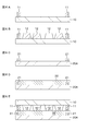
- 6A to 6E are schematic partial cross-sectional views for explaining a manufacturing process of a semiconductor device.
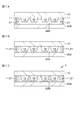
- FIG. 7A to 7C are schematic partial cross-sectional views for explaining the manufacturing process of the semiconductor device, following FIG. 6E. 8A to 8D are schematic partial cross-sectional views for explaining the manufacturing process of the semiconductor device.
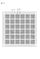
- FIG. 9 is a schematic plan view for explaining the structure of the chip-shaped semiconductor element according to the second embodiment.
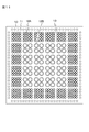
- FIG. 10 is a schematic plan view for explaining the structure of the chip-like semiconductor element according to the third embodiment.
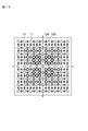
- FIG. 11 is a schematic plan view for explaining the structure of the chip-like semiconductor element according to the fourth embodiment.
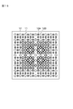
- 12A and 12B are schematic plan views for explaining the structure of the chip-like semiconductor element according to the fifth embodiment.
- FIG. 12A shows the arrangement relationship of the electrodes, and FIG. The arrangement relationship is shown.
- FIG. 12A shows the arrangement relationship of the electrodes, and FIG. The arrangement relationship is shown.
- FIG. 13 is a schematic plan view for explaining the structure of the chip-like semiconductor element according to the fifth embodiment, and shows the positional relationship between electrodes and protrusions.
- 14A and 14B are schematic plan views for explaining the structure of the chip-like semiconductor element according to the sixth embodiment.
- FIG. 14A shows the arrangement relationship of the electrodes
- FIG. 14B shows the protrusions. The arrangement relationship is shown.
- FIG. 15 is a schematic plan view for explaining the structure of the chip-shaped semiconductor element according to the sixth embodiment, and shows the positional relationship between electrodes and protrusions.
- 16A and 16B are schematic plan views for explaining the structure of the chip-shaped semiconductor element according to the seventh embodiment.
- FIG. 16A shows an arrangement relationship of electrodes, and FIG. The arrangement relationship is shown.
- FIG. 16A shows an arrangement relationship of electrodes, and FIG. The arrangement relationship is shown.
- FIG. 17 is a schematic plan view for explaining the structure of the chip-like semiconductor element according to the seventh embodiment, and shows the positional relationship between electrodes and protrusions.
- 18A and 18B are schematic plan views for explaining the structure of the chip-like semiconductor element according to the eighth embodiment.
- FIG. 18A shows the arrangement relationship of the electrodes
- FIG. 18B shows the protrusions. The arrangement relationship is shown.
- FIG. 19 is a schematic plan view for explaining the structure of the chip-shaped semiconductor element according to the eighth embodiment, and shows the positional relationship between electrodes and protrusions.
- FIG. 20 is a schematic plan view for explaining the structure of the semiconductor device according to the ninth embodiment provided with a pair of chip-like semiconductor elements.
- FIG. 21A and 21B are schematic plan views for explaining the structure of one of the pair of chip-like semiconductor elements according to the ninth embodiment, and FIG. 21A shows the arrangement relationship of the electrodes, FIG. 21B shows the arrangement relationship of the protrusions.
- 22A and 22B are schematic plan views for explaining the other structure of the pair of chip-like semiconductor elements according to the ninth embodiment, and FIG. 22A shows the arrangement relationship of the electrodes.
- FIG. 22B shows the arrangement relationship of the protrusions.
- 23A and 23B are schematic partial cross-sectional views for explaining a manufacturing process of the semiconductor device according to the tenth embodiment.
- FIG. 24 is a schematic diagram for explaining the structure of the protrusions of the chip-like semiconductor element according to the eleventh embodiment.
- FIG. 25B are schematic diagrams for explaining the function of the protrusions of the chip-like semiconductor element according to the eleventh embodiment.
- FIG. 26 is a diagram of the twelfth embodiment, and is a schematic perspective view of an electronic apparatus in which the semiconductor device of the present disclosure is used.
- FIG. 27 is a schematic block diagram illustrating a circuit configuration of the electronic device illustrated in FIG. 28A and 28B are process diagrams for explaining a manufacturing process of a semiconductor device.
- a semiconductor device according to the present disclosure, a semiconductor device used in an electronic apparatus according to the present disclosure, and a semiconductor device manufactured by the method for manufacturing a semiconductor device according to the present disclosure (hereinafter, simply referred to as a semiconductor device according to the present disclosure).
- the chip-like semiconductor element may have a protrusion formed so that the tip does not reach the wiring board in a state where the chip-like semiconductor element is flip-chip mounted.
- the chip-like semiconductor element is bonded to the wiring board by fusing the solder bump provided on the wiring board and the solder bump provided on the chip-like semiconductor element by a reflow process.
- the chip-like semiconductor element can be configured to be mounted in a state where the positioning is performed.
- the underfill material may be selectively applied on the wiring substrate or may be applied collectively. From the viewpoint of improving productivity, it is preferable that the coating is applied onto the wiring substrate at once.
- the underfill material preferably has a flux function. According to this configuration, since the oxide on the metal surface in contact with the underfill material is removed, the solder bumps can be well fused by the reflow process.
- the chip-shaped semiconductor element according to the present disclosure is a chip-shaped semiconductor element that is flip-chip mounted on a wiring board on which an underfill material is applied.
- a plurality of solder bumps and a plurality of protrusions made of an insulating material are provided on the surface of the chip-like semiconductor element facing the wiring board. And it can be set as the structure which has the protrusion formed so that the front-end
- the chip-shaped semiconductor element according to the present disclosure and the chip-shaped semiconductor element used for the semiconductor chip of the present disclosure may be simply referred to as the chip-shaped semiconductor element of the present disclosure
- It may be a configuration having a protrusion formed higher than the solder bump provided, a configuration having a protrusion formed at the same height as the solder bump, or lower than the solder bump.
- the structure which has the protrusion currently formed may be sufficient.
- the chip-shaped semiconductor element of the present disclosure including the various preferable configurations described above, It can be set as the structure by which the protrusion is provided with the fixed density in the area
- the region where the protrusions are arranged on the surface of the chip-like semiconductor element can be configured such that the protrusions are provided at different densities depending on the position in the region.
- the gap between adjacent protrusions may be provided so as to cross the region where the protrusions are disposed.
- the density of the protrusions in the central region of the surface of the chip-like semiconductor element can be higher than the density of the protrusions in the peripheral region surrounding the central region.
- a protrusion having the same shape may be provided on the surface of the chip-shaped semiconductor element.
- a plurality of types of protrusions having different shapes can be provided on the surface of the chip-like semiconductor element.
- it can be set as the structure by which the multiple types of protrusion from which height differs is provided.
- the protrusion may be formed so that the shape becomes smaller as the distance from the surface of the chip-shaped semiconductor element increases.
- the protrusion may have a truncated pyramid shape in which the surface side of the chip-shaped semiconductor element is the bottom surface and the cross-sectional shape decreases as the distance from the surface of the chip-shaped semiconductor element increases.
- the protrusions may have a symmetric shape or an asymmetric shape.
- a semiconductor device, a chip-shaped semiconductor element, an electronic device including the semiconductor device, and a method for manufacturing a semiconductor device (hereinafter, these may be simply referred to as the present disclosure) according to the present disclosure, including the various preferable configurations described above.
- the configuration may be such that one chip-like semiconductor element is mounted on one wiring substrate, or the configuration may be such that a plurality of chip-like semiconductor elements are mounted on one wiring substrate.
- positioned the chip-shaped semiconductor element and the surface mounting component may be sufficient.
- the protrusions provided on the chip-like semiconductor element of the present disclosure are formed using, for example, a photosensitive resin such as PI, phenol, PBO, BCB, or acrylic, and using a photolithography technique such as exposure. can do.
- a photosensitive resin such as PI, phenol, PBO, BCB, or acrylic
- a photolithography technique such as exposure. can do.
- it can be formed using a 3D printer technique using a polyamide-based resin, an ABS-based resin, or the like.
- it can be formed by an etching technique using a glass-based material.
- the method of applying the underfill material on the wiring board is not particularly limited as long as the implementation of the present disclosure is not hindered.
- it can apply
- the material constituting the underfill material used in the present disclosure is not particularly limited as long as it does not hinder the implementation of the present disclosure. Specifically, any material may be used as long as the viscosity decreases to such an extent that self-alignment is not hindered during the reflow process and the curing process can be performed after the reflow process.
- a material constituting the underfill material for example, an epoxy-based material can be exemplified.
- a thermosetting underfill material is cured by a reaction of a curing agent by heating for a long time. The heating time during reflow is short, the curing reaction is slight, and the viscosity decreases with increasing temperature.
- the first embodiment relates to a semiconductor device, a chip-like semiconductor element, and a method for manufacturing a semiconductor device according to the first aspect of the present disclosure.
- FIG. 1 is a schematic exploded perspective view for explaining a semiconductor device according to a first aspect of the present disclosure.
- the semiconductor device 1 includes a wiring substrate 20 and a chip-like semiconductor element 10 flip-chip mounted on the wiring substrate 20.
- a plurality of solder bumps and a plurality of protrusions made of an insulating material are provided on the surface of the chip-like semiconductor element 10 facing the wiring substrate 20.
- the chip-like semiconductor element 10 is disposed so as to face the wiring substrate 20 through the underfill material 22 in a state where the underfill material 22 having a characteristic that the viscosity decreases as the temperature rises is applied on the wiring substrate 20. Then, the chip is flip-chip mounted on the wiring board 20 by performing a reflow process.
- the chip-like semiconductor element 10 has a protrusion formed so that the tip does not reach the wiring board 20 in a state where the chip-like semiconductor element 10 is flip-chip mounted.
- the chip-like semiconductor element 10 is positioned with respect to the wiring board 20 by fusing the solder bumps provided on the wiring board 20 and the solder bumps provided on the chip-like semiconductor element 10 by reflow processing. Implemented in.
- FIG. 2 is a process diagram for explaining a basic manufacturing process of the semiconductor device according to the first aspect of the present disclosure.
- the underfill material 22 is collectively applied onto the wiring board 20 (see, for example, FIG. 5 described later).
- the chip-like semiconductor element 10 is disposed so as to face the wiring board 20 with the underfill material 22 interposed therebetween. At this time, it is sufficient that the chip-like semiconductor element 10 is arranged with such an accuracy that self-alignment is effective. In other words, it is not necessary that the electrodes of the wiring board 20 and the electrodes of the chip-like semiconductor element 10 are positioned with high precision so as to face each other accurately.
- a batch reflow process is performed. As will be described later in detail with reference to FIGS.
- a plurality of solder bumps and a plurality of protrusions made of an insulating material are provided on the surface of the chip-like semiconductor element 10 facing the wiring substrate 20.
- the chip-like semiconductor element 10 before flip chip mounting will be described in detail.
- FIG. 3A and 3B are schematic perspective views for explaining the arrangement of the electrodes and protrusions of the chip-like semiconductor element 10.
- FIG. 3A shows a state before the projection is formed
- FIG. 3B shows a state after the projection is formed.
- solder bumps 11 are provided at predetermined intervals along each side of the rectangular chip-shaped semiconductor element 10 (see FIG. 3A).
- a plurality of protrusions 12 made of an insulating material are formed inside a region surrounded by the solder bumps 11 using, for example, a photolithography technique (see FIG. 3B).
- the protrusion 12 is formed to have a shape that becomes smaller as the distance from the surface of the chip-like semiconductor element 10 increases, and is a symmetrical shape.
- the protrusion 12 has a function of sucking and filling the underfill material 22 pre-coated on the wiring board 20 to the chip-like semiconductor element side by a capillary phenomenon.
- the protrusion 12 is formed higher than the solder bump 11.
- FIG. 4 is a schematic perspective view for explaining the electrode arrangement of the wiring board.
- FIG. 5 is a schematic perspective view for explaining the arrangement of the electrodes of the wiring board and the pre-painted underfill material layer.
- a portion of the wiring board 20 that faces the chip-like semiconductor element 10 is denoted by reference numeral 20A.
- the portion represented by reference numeral 20A may be simply referred to as the facing portion 20A.
- 20 A of opposing parts are substantially rectangular, and the solder bump 21 is formed so that it may correspond with the chip-shaped semiconductor element 10 along each edge
- the underfill material 22 is collectively applied to the wiring board 20 in this state (see FIG. 5).
- a method for manufacturing a semiconductor device includes: A chip-like semiconductor element 10 in which a plurality of solder bumps 11 and a plurality of protrusions 12 made of an insulating material are provided on the surface facing the wiring board 20 is an underlayer having a characteristic that the viscosity decreases as the temperature rises.
- 6A to 6E are schematic partial cross-sectional views for explaining a manufacturing process of a semiconductor device.
- 7A to 7C are schematic partial cross-sectional views for explaining the manufacturing process of the semiconductor device, following FIG. 6E.
- FIG. 6E For the convenience of illustration, in these drawings, only the portion of the facing portion 20A is shown in the wiring board. The shape of each component is shown in a simplified manner.
- Step-100 A chip-like semiconductor element 10 is prepared, and solder bumps 11 serving as electrodes are formed thereon (see FIG. 6A). Next, a plurality of protrusions 12 made of an insulating material are formed inside a region surrounded by the solder bumps 11 using, for example, a photolithography technique (see FIG. 6B).
- Step-110 (see FIGS. 6C and 6D) A wiring board 20 is prepared, and solder bumps 21 serving as electrodes are formed on the facing portion 20A (see FIG. 6C). Next, the underfill material 22 is collectively applied over the entire surface including the facing portion 20A (see FIG. 6D).
- the underfill material 22 is collectively applied onto the wiring board 20. There is no need to selectively apply the facing portion 20A. Moreover, the underfill material 22 which has a flux function is used for application
- Step-120 (see FIG. 6E) Thereafter, the chip-like semiconductor element 10 is disposed so as to face the wiring substrate 20 with the underfill material 22 interposed therebetween.
- Step-130 (see FIGS. 7A and 7B) Next, reflow processing is performed.
- the underfill material in a fluid state is represented by reference numeral 22A.
- the chip-like semiconductor element 10 is further submerged by the fusion of the solder bumps 11 and 21, filling of the underfill material 22A between the chip-like semiconductor element 10 and the wiring board 20 is promoted.
- the gap between the protrusions of the chip-like semiconductor element 10 becomes a gas flow path in the filling process of the underfill material 22A. Accordingly, voids in the underfill material 22 during chip mounting can be reduced.
- the amount of suction and the reaching height of the underfill material 22 ⁇ / b> A during the reflow process can be controlled by the design of the protrusion 12.
- the protrusion 12 is formed so that the tip does not reach the wiring substrate 20 in a state where the chip-like semiconductor element 10 is flip-chip mounted.
- it may further include a protrusion such as a gap interval setting application in which the tip reaches the wiring board 20 within a range not inhibiting the self-alignment effect.
- Step-140 (see FIG. 7C) Next, the underfill material 22A is cured.
- the curing process may be appropriately selected according to the type of the underfill material.
- the underfill material after curing is represented by reference numeral 22B. As a result, the semiconductor device 1 in which the chip-like semiconductor element 10 is mounted on the wiring board 20 can be obtained.
- the manufacturing method of the present disclosure is a method of pre-coating an underfill material, and the tact time required for sealing is shorter than that of the capillary underfill method. Furthermore, the manufacturing method of the present disclosure does not require pressure heating for each chip when mounting the chip. And since the self-alignment by solder bonding is exhibited, the positioning accuracy at the time of disposing the chip-like semiconductor element is eased. Therefore, according to the manufacturing method of this indication, a process can be simplified and tact time and lead time can be shortened significantly.
- the protrusions 12 are formed higher than the solder bumps 11.
- the present invention is not limited to this.
- the protrusion 12 may be the same height as the solder bump 11, or the protrusion 12 may be lower than the solder bump 11.
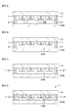
- FIG. 8 shows a process chart when the protrusion 12 is made lower than the solder bump 11.
- FIG. 8A corresponds to FIG. 6E. Since the protrusion 12 is lower than the solder bump 11, the solder bump 11 contacts the underfill material 22 before the protrusion 12.
- FIG. 8B is a diagram corresponding to FIG. 7A
- FIG. 8C is a diagram corresponding to FIG. 7B.
- FIG. 8D corresponds to FIG. 7C.
- the second embodiment relates to a chip-shaped semiconductor element according to the first aspect of the present disclosure.
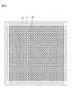
- FIG. 9 is a schematic plan view for explaining the structure of the chip-like semiconductor element according to the second embodiment.
- the solder bumps 11 are continuously arranged along each side of the outer peripheral portion of the chip-like semiconductor element 10.
- the protrusions 12 are provided at a constant density in a region where the protrusions are disposed on the surface of the chip-like semiconductor element 10 (more specifically, a region surrounded by the solder bumps).
- the protrusions 12 having the same shape are uniformly arranged at the same pitch on the surface of the chip-like semiconductor element 10.
- the protrusions 12 can be formed by using a photolithography technique in which, for example, a photosensitive insulating resin material is applied, then exposed using a photomask on which a necessary pattern is drawn, and then developed. it can.
- the third embodiment also relates to a chip-shaped semiconductor element according to the first aspect of the present disclosure.
- the protrusions are provided at a constant density in the region where the protrusions are arranged.
- the protrusions are provided with different densities according to the positions in the region.
- FIG. 10 is a schematic plan view for explaining the structure of the chip-like semiconductor element according to the third embodiment.
- the solder bumps 11 are continuously arranged along each side of the outer peripheral portion of the chip-like semiconductor element 10, and the protrusions 12 are formed in the region where the protrusions are arranged on the surface of the chip-like semiconductor element 10. Is provided.
- the region surrounded by the solder bumps 11 is divided into a plurality of blocks.
- a gap 13 is provided between the blocks.
- protrusions 12 having the same shape are uniformly arranged at the same pitch.
- the gap 13 is set wider than the interval between the protrusions in the block. In this structure, it arrange
- the fourth embodiment is a modification of the third embodiment.
- protrusions having the same shape are uniformly arranged at the same pitch in each block.
- the fourth embodiment is mainly different in that a plurality of types of protrusions having different shapes are provided.
- FIG. 11 is a schematic plan view for explaining the structure of the chip-like semiconductor element according to the fourth embodiment.
- the solder bumps 11 are continuously arranged along each side of the outer peripheral portion of the chip-shaped semiconductor element 10, and the protrusions are formed in the region where the protrusions are disposed on the surface of the chip-shaped semiconductor element 10. Is provided.
- the area surrounded by the solder bumps 11 is divided into a plurality of blocks. A gap 13 is provided between the blocks.
- a protrusion 12B having a larger diameter is arranged in the block near the center of the chip-like semiconductor element 10.
- the protrusions 12 ⁇ / b> B are also formed so as to become smaller in shape as they move away from the surface of the chip-like semiconductor element 10, and have a symmetrical shape.
- the heights of the protrusions 12A and the protrusions 12B may be the same or different.
- the gap 13 is set wider than the interval between the protrusions in the block. Similar to the third embodiment, these gaps 13 serve as a gas flow path when the chip-shaped semiconductor element is mounted, so that voids of the underfill material when mounting the chip-shaped semiconductor element are efficiently reduced. be able to.
- the fifth embodiment also relates to a chip-shaped semiconductor element according to the first aspect of the present disclosure.
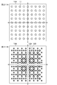
- FIG. 12A and 12B are schematic plan views for explaining the structure of the chip-like semiconductor element according to the fifth embodiment.
- FIG. 12A shows the arrangement relationship of the electrodes
- FIG. The arrangement relationship is shown.
- FIG. 13 is a schematic plan view for explaining the structure of the chip-like semiconductor element according to the fifth embodiment, and shows the positional relationship between electrodes and protrusions.
- the solder bumps are continuously arranged along each side of the outer peripheral portion of the chip-like semiconductor element.
- the solder bumps 11 are arranged in a matrix on the surface of the chip-like semiconductor element 10. And in the area
- the protrusions are provided with different densities according to the positions in the region.
- the surface of the chip-like semiconductor element 10 is provided with a plurality of types of protrusions having different shapes, and the density of the protrusions in the central region of the surface of the chip-like semiconductor element 10 is in the peripheral region surrounding the central region. It is higher than the density of protrusions.
- the surface of the chip-like semiconductor element 10 is divided into four blocks. Basically, the projections 12B having a large size are arranged with high density in the region close to the center of the chip-shaped semiconductor element 10, and the projections 12A having a small size are discarded when the chip-shaped semiconductor element 10 is separated from the center. In addition, the density is reduced.
- the sixth embodiment is a modification of the fifth embodiment.
- the solder bumps are arranged in a matrix on the surface of the chip-like semiconductor element.
- the sixth embodiment is different in that a solder bump is not disposed in part and a protrusion is formed instead.
- FIG. 14A and 14B are schematic plan views for explaining the structure of the chip-like semiconductor element according to the sixth embodiment.
- FIG. 14A shows the arrangement relationship of the electrodes
- FIG. 14B shows the protrusions. The arrangement relationship is shown.
- FIG. 15 is a schematic plan view for explaining the structure of the chip-shaped semiconductor element according to the sixth embodiment, and shows the positional relationship between electrodes and protrusions.
- solder bumps 11 are not arranged in the region indicated by reference numeral 13.
- the projections 12A and 12B are arranged so as to fill the region 13.
- the seventh embodiment is a modification of the sixth embodiment.
- FIG. 16A and 16B are schematic plan views for explaining the structure of the chip-shaped semiconductor element according to the seventh embodiment.
- FIG. 16A shows an arrangement relationship of electrodes
- FIG. The arrangement relationship is shown.
- FIG. 17 is a schematic plan view for explaining the structure of the chip-like semiconductor element according to the seventh embodiment, and shows the positional relationship between electrodes and protrusions.
- a protrusion 12C formed so as to follow the planar shape is formed.
- the eighth embodiment also relates to a chip-shaped semiconductor element according to the first aspect of the present disclosure.
- FIG. 18A and 18B are schematic plan views for explaining the structure of the chip-like semiconductor element according to the eighth embodiment.
- FIG. 18A shows the arrangement relationship of the electrodes
- FIG. 18B shows the protrusions. The arrangement relationship is shown.
- FIG. 19 is a schematic plan view for explaining the structure of the chip-shaped semiconductor element according to the eighth embodiment, and shows the positional relationship between electrodes and protrusions.
- the process when the protrusion is lower than the solder bump has been described with reference to FIGS. 8A to 8D.
- the solder bump comes into contact with the underfill material prior to the protrusion, it is preferable to arrange the solder bump or the like so as to secure a passage communicating with the outside of the chip.
- the solder bumps 11 are arranged along each side of the outer peripheral portion of the chip-like semiconductor element 10. However, the solder bumps 11 are arranged at intervals in these portions so as to secure passages that lead to the outside of the chip at the center of each of the four corners and the left and right sides of the chip-like semiconductor element 10.
- the protrusions 12C are provided so as to secure a flow path that leads to the outside of the chip.
- 12D, 12E are arranged.
- the ninth embodiment relates to a semiconductor device and a chip-like semiconductor element according to the first aspect of the present disclosure.
- the semiconductor device is configured by mounting one chip-like semiconductor element on the wiring board.
- the semiconductor device of the ninth embodiment has a so-called multichip configuration.
- FIG. 20 is a schematic plan view for explaining the structure of the semiconductor device according to the ninth embodiment provided with a pair of chip-like semiconductor elements.
- a semiconductor device 1A according to the ninth embodiment is a semiconductor device having a multi-chip configuration, and chip-like semiconductor elements 10A and 10B are mounted on a wiring board. In FIG. 20, the wiring board is not shown.
- FIG. 21A and 21B are schematic plan views for explaining the structure of one of the pair of chip-like semiconductor elements according to the ninth embodiment, and FIG. 21A shows the arrangement relationship of the electrodes, FIG. 21B shows the arrangement relationship of the protrusions.
- the solder bumps 11 are arranged in a matrix on the surface of the chip-like semiconductor element 10A.
- the protrusions 12A and 12B are disposed so as to fill the space between the solder bumps in the region where the protrusions are disposed on the surface of the chip-like semiconductor element 10A (more specifically, the region where the solder bumps are not disposed). Has been.
- FIG. 22A and 22B are schematic plan views for explaining the other structure of the pair of chip-like semiconductor elements according to the ninth embodiment, and FIG. 22A shows the arrangement relationship of the electrodes. FIG. 22B shows the arrangement relationship of the protrusions.
- solder bumps 11 are not partially arranged, and instead, protrusions are formed.
- the surface of the chip-like semiconductor element is divided into four blocks. And it is the structure which made the size of the protrusion of the area
- the tenth embodiment relates to a semiconductor device according to the first aspect of the present disclosure.
- the semiconductor device according to the tenth embodiment is a semiconductor device in which a connection by flip chip mounting and a connection by wire bonding are mixed.
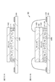
- 23A and 23B are schematic partial cross-sectional views for explaining a manufacturing process of the semiconductor device according to the tenth embodiment.
- FIG. 23A shows a state during the reflow process.
- the semiconductor device 1B is wired by wiring to the electrode 23 by the wire bonding 40. Can be obtained (see FIG. 23B).
- the eleventh embodiment relates to a chip-shaped semiconductor element according to the first aspect of the present disclosure.
- the underfill material is basically pushed out isotropically around the protrusions.
- the underfill material has a non-uniform filling property, it is possible to take measures such as adjusting the arrangement density of the protrusions on the surface of the chip-like semiconductor element and making the shape of the protrusions asymmetric.
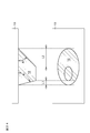
- FIG. 24 is a schematic diagram for explaining the structure of the protrusions of the chip-like semiconductor element according to the tenth embodiment.
- the protrusion 12 shown in the figure differs from the chip-like semiconductor element surface in the angle formed by the left slope (indicated by reference symbol A1) and the angle formed by the right slope (indicated by reference symbol A2).
- 12 has an asymmetric shape in which the center position is different between the surface of the tip end 12 and the surface on the chip-like semiconductor element side.
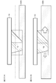
- FIG. 25A and FIG. 25B are schematic diagrams for explaining the function of the protrusions of the chip-like semiconductor element according to the eleventh embodiment.
- the fluidized underfill material 22A is pushed out more to the right side of the protrusion 12. Thereby, the degree of filling of the underfill material 22 can be adjusted.
- the asymmetric shape of the protrusion 12 may be selected as appropriate based on the specifications of the chip-like semiconductor element.
- the asymmetric protrusion can be formed using, for example, 3D printer technology.
- the twelfth embodiment according to the present disclosure is an electronic apparatus in which the semiconductor device obtained by each of the above-described embodiments is mounted.
- FIG. 26 illustrates a schematic configuration of the electronic device.
- the electronic device 1100 includes, for example, necessary parts disposed inside and outside an outer casing 1101 formed in a horizontally long flat shape, and is used as, for example, a game device.
- a display panel 1102 is provided in the center in the left-right direction on the front surface of the outer casing 1101, and four operation keys 1103 and four operations arranged on the left and right sides of the display panel 1102 are spaced apart from each other in the circumferential direction.
- a key 1104 is provided.
- four operation keys 1105 are provided at the lower end of the front surface of the outer casing 1101.
- the operation keys 1103, the operation keys 1104, and the operation keys 1105 function as direction keys and determination keys used for selection of menu items displayed on the display panel 1102, game progress, and the like.
- connection terminal 1106 for connecting an external device, a supply terminal 1107 for supplying power, a light receiving window 1108 for performing infrared communication with the external device, and the like are provided.
- FIG. 27 is a schematic block diagram showing a circuit configuration of the electronic device shown in FIG.
- the electronic device 1100 includes a main CPU (Central Processing Unit) 1110 and a system controller 1120. For example, power is supplied to the main CPU 1110 and the system controller 1120 from different systems from a battery (not shown).
- the electronic device 1100 further includes a setting information holding unit 1130 including a memory that holds various types of information set by the user.
- the main CPU 1110, the system controller 1120, and the setting information holding unit 1130 are configured as an integrated semiconductor device according to the present disclosure.
- the main CPU 1110 includes a menu processing unit 111 that generates a menu screen for allowing a user to set various information and select an application, and an application processing unit 112 that executes an application.
- the set information is sent to the setting information holding unit 1130 by the main CPU 1110 and held in the setting information holding unit 1130.
- the system controller 1120 includes an operation input receiving unit 121, a communication processing unit 122, and a power control unit 123.
- the operation input receiving unit 121 detects the state of the operation key 1103, the operation key 1104, and the operation key 1105, the communication processing unit 122 performs communication processing with an external device, and the power control unit 123 The supplied power is controlled.
- Semiconductor device By being flip-chip mounted on the wiring board, Semiconductor device.
- the chip-like semiconductor element has a protrusion formed so that the tip does not reach the wiring board in a state where the chip-like semiconductor element is flip-chip mounted.
- [A3] The chip-like semiconductor element is mounted in a state where the solder bump provided on the wiring board and the solder bump provided on the chip-like semiconductor element are fused with each other by reflow processing.
- [A4] Underfill material is applied all over the circuit board.
- [A5] Underfill material has a flux function, The semiconductor device according to any one of [A1] to [A4].
- the protrusions are provided with a constant density.
- the protrusions are provided with different densities according to the positions in the area.
- the gap between adjacent protrusions on the surface of the chip-like semiconductor element is provided so as to cross the region where the protrusions are disposed. The semiconductor device according to [A7] above.
- the density of the protrusions in the central region of the surface of the chip-like semiconductor element is higher than the density of the protrusions in the peripheral region surrounding the central region.
- [A10] Projections having the same shape are provided on the surface of the chip-like semiconductor element.
- [A12] Plural kinds of protrusions having different heights are provided on the surface of the chip-like semiconductor element.
- the protrusion on the surface of the chip-shaped semiconductor element is formed so that the shape becomes smaller as it is away from the surface of the chip-shaped semiconductor element.
- the protrusions on the surface of the chip-like semiconductor element are symmetrical.
- the protrusion on the surface of the chip-like semiconductor element has an asymmetric shape.
- the chip-like semiconductor element has a protrusion formed so that the tip does not reach the wiring board in a state where the chip-like semiconductor element is flip-chip mounted.
- the chip-shaped semiconductor element as described in [B1] above.
- the protrusions are provided with a constant density.
- the protrusions are provided with different densities according to the positions in the area.
- the gap between adjacent protrusions is provided so as to cross the region where the protrusions are disposed.
- the density of the protrusions in the central region of the surface of the chip-like semiconductor element is higher than the density of the protrusions in the peripheral region surrounding the central region.
- [B7] Projections having the same shape are provided on the surface of the chip-like semiconductor element.
- a plurality of types of protrusions having different shapes are provided on the surface of the chip-like semiconductor element.
- Plural types of protrusions with different heights are provided, The chip-shaped semiconductor element as described in [B8] above.
- the protrusion is formed such that the shape becomes smaller as the distance from the surface of the chip-like semiconductor element increases.
- the projection is symmetrical.
- the protrusion has an asymmetric shape, The chip-shaped semiconductor element according to any one of [B1] to [B10].
- An electronic device comprising a semiconductor device comprising a wiring substrate and a chip-like semiconductor element flip-chip mounted on the wiring substrate, On the surface of the chip-like semiconductor element facing the wiring substrate, a plurality of solder bumps and a plurality of protrusions made of an insulating material are provided, The chip-like semiconductor element is subjected to a reflow process after being disposed so as to face the wiring board through the underfill material in a state in which the underfill material having a characteristic that the viscosity decreases as the temperature rises is applied on the wiring board.
- the underfill material having a characteristic that the viscosity decreases as the temperature rises is applied on the wiring board.
- the chip-like semiconductor element has a protrusion formed so that the tip does not reach the wiring board in a state where the chip-like semiconductor element is flip-chip mounted.
- [C3] The chip-like semiconductor element is mounted in a state where the solder bump provided on the wiring board and the solder bump provided on the chip-like semiconductor element are fused with each other by reflow processing.
- [C4] Underfill material is applied all over the circuit board.
- [C5] Underfill material has a flux function, The electronic device according to any one of [C1] to [C4].
- the protrusions are provided with a constant density.
- the protrusions are provided with different densities according to the positions in the area.
- the gap between adjacent protrusions on the surface of the chip-like semiconductor element is provided so as to cross the region where the protrusions are disposed. The electronic device according to [C7] above.
- the density of the protrusions in the central region of the surface of the chip-like semiconductor element is higher than the density of the protrusions in the peripheral region surrounding the central region.
- [C10] Projections having the same shape are provided on the surface of the chip-like semiconductor element.
- [C12] Plural kinds of protrusions having different heights are provided on the surface of the chip-like semiconductor element.
- the protrusion on the surface of the chip-shaped semiconductor element is formed so that the shape becomes smaller as it is away from the surface of the chip-shaped semiconductor element.
- the protrusions on the surface of the chip-like semiconductor element are symmetrical.
- [C15] The protrusion on the surface of the chip-like semiconductor element has an asymmetric shape.
- a chip-like semiconductor element in which a plurality of solder bumps and a plurality of protrusions made of an insulating material are provided on the surface facing the wiring board is wired with an underfill material having a characteristic that the viscosity decreases as the temperature rises.
- Including a step of flip-chip mounting on the wiring board by performing a reflow process after being arranged so as to face the wiring board through the underfill material in a state of being applied on the board A manufacturing method of a manufacturing method of a semiconductor device.
- the chip-like semiconductor element has a protrusion formed so that the tip does not reach the wiring board in a state where the chip-like semiconductor element is flip-chip mounted.
- the protrusions are provided with a constant density.
- [D7] In the area where the protrusions are arranged on the surface of the chip-like semiconductor element, the protrusions are provided with different densities according to the positions in the area.
- [D8] The gap between adjacent protrusions on the surface of the chip-like semiconductor element is provided so as to cross the region where the protrusions are disposed. The manufacturing method of the semiconductor device as described in said [D7].
- [D12] Plural kinds of protrusions having different heights are provided on the surface of the chip-like semiconductor element.
- [D13] The protrusion on the surface of the chip-shaped semiconductor element is formed so that the shape becomes smaller as it is away from the surface of the chip-shaped semiconductor element.
- the protrusions on the surface of the chip-like semiconductor element are symmetrical.
- [D15] The protrusion on the surface of the chip-like semiconductor element has an asymmetric shape.
- operation keys 1106 ... terminals, 1107 ... supply terminals for power supply, 1108 ... light receiving window, 1110 ... main CPU, 111 ... Menu processing unit, 1112 ... Application processing unit, 1120 ... System controller, 1121 ... Operation input receiving unit, 1122 ... Communication processing unit, 1123 ... Power control unit, 1130 ..Setting information holding unit
Landscapes
- Engineering & Computer Science (AREA)
- Manufacturing & Machinery (AREA)
- Microelectronics & Electronic Packaging (AREA)
- Wire Bonding (AREA)
- Structures Or Materials For Encapsulating Or Coating Semiconductor Devices Or Solid State Devices (AREA)
Abstract
Description
配線基板と、
配線基板上にフリップチップ実装されたチップ状半導体素子と、
を備えており、
配線基板と対向する側のチップ状半導体素子の面には、複数のハンダバンプと、絶縁性材料から成る複数の突起物とが設けられており、
チップ状半導体素子は、温度上昇に伴い粘度が低下する特性を有するアンダーフィル材が配線基板上に塗布された状態でアンダーフィル材を介して配線基板と対向するように配置された後にリフロー処理が施されることによって、配線基板上にフリップチップ実装されている、
半導体装置である。
アンダーフィル材が塗布されている配線基板上にフリップチップ実装されるチップ状半導体素子であって、
配線基板と対向する側のチップ状半導体素子の面には、複数のハンダバンプと、絶縁性材料から成る複数の突起物とが設けられている、
チップ状半導体素子である。
配線基板と配線基板上にフリップチップ実装されたチップ状半導体素子とから成る半導体装置を備えた電子機器であって、
配線基板と対向する側のチップ状半導体素子の面には、複数のハンダバンプと、絶縁性材料から成る複数の突起物とが設けられており、
チップ状半導体素子は、温度上昇に伴い粘度が低下する特性を有するアンダーフィル材が配線基板上に塗布された状態でアンダーフィル材を介して配線基板と対向するように配置された後にリフロー処理が施されることによって、配線基板上にフリップチップ実装されている、
電子機器である。
配線基板と対向する側の面に複数のハンダバンプと絶縁性材料から成る複数の突起物とが設けられているチップ状半導体素子を、温度上昇に伴い粘度が低下する特性を有するアンダーフィル材が配線基板上に塗布された状態でアンダーフィル材を介して配線基板と対向するように配置した後、リフロー処理を施すことによって配線基板上にフリップチップ実装する工程を含む、
半導体装置の製造方法である。
1.本開示に係る、半導体装置、チップ状半導体素子、半導体装置を備えた電子機器、及び、半導体装置の製造方法、全般に関する説明
2. 第1の実施形態
3. 第2の実施形態
4. 第3の実施形態
5. 第4の実施形態
6. 第5の実施形態
7. 第6の実施形態
8. 第7の実施形態
9. 第8の実施形態
10. 第9の実施形態
11.第10の実施形態
12.第11の実施形態
13.第12の実施形態
14.その他
本開示に係る半導体装置、本開示に係る電子機器に用いられる半導体装置、及び、本開示に係る半導体装置の製造方法により製造される半導体装置(以下、これらを単に、本開示の半導体装置と呼ぶ場合がある)において、チップ状半導体素子は、チップ状半導体素子がフリップチップ実装された状態において先端が配線基板に達しないように形成されている突起物を有する構成とすることができる。
チップ状半導体素子の面における突起物が配置される領域には、一定の密度で突起物が設けられている構成とすることができる。
第1の実施形態は、本開示の第1の態様に係る、半導体装置、チップ状半導体素子、及び、半導体装置の製造方法に関する。
配線基板20と対向する側の面に複数のハンダバンプ11と絶縁性材料から成る複数の突起物12とが設けられているチップ状半導体素子10を、温度上昇に伴い粘度が低下する特性を有するアンダーフィル材22が配線基板20上に塗布された状態でアンダーフィル材22を介して配線基板20と対向するように配置した後、リフロー処理を施すことによって配線基板20上にフリップチップ実装する工程を含む。
チップ状半導体素子10を準備し、その上に、電極となるハンダバンプ11を形成する(図6A参照)。次いで、例えばフォトリソグラフィー技術を用いて、ハンダバンプ11で囲まれた領域の内側に、絶縁性材料から成る複数の突起物12を形成する(図6B参照)。
配線基板20を準備し、対向部20A上に、電極となるハンダバンプ21を形成する(図6C参照)。次いで、対向部20A上を含む全面に、アンダーフィル材22を一括して塗布する(図6D参照)。
その後、チップ状半導体素子10を、アンダーフィル材22を介して配線基板20と対向するように配置する。
次いで、リフロー処理を行う。
次いで、アンダーフィル材22Aの硬化処理を行う。硬化処理は、アンダーフィル材の種類に応じて、適宜好適な方法を選択すればよい。硬化後のアンダーフィル材を符号22Bで表す。これによって、配線基板20にチップ状半導体素子10が実装されて成る半導体装置1を得ることができる。
第2の実施形態は、本開示の第1の態様に係るチップ状半導体素子に関する。
第3の実施形態も、本開示の第1の態様に係るチップ状半導体素子に関する。第2の実施形態では、突起物が配置される領域には、一定の密度で突起物が設けられいた。これに対し、第3の実施形態では、領域内の位置に応じた異なる密度で突起物が設けられている。
第4の実施形態は、第3の実施形態の変形例である。第3の実施形態にあっては、各ブロック内には、同一形状の突起物が、一様に同一ピッチで配置されていた。これに対して、第4の実施形態では、形状の異なる複数種の突起物が設けられている点が主に相違する。
第5の実施形態も、本開示の第1の態様に係るチップ状半導体素子に関する。
第6の実施形態は、第5の実施形態の変形例である。第5の実施形態にあっては、ハンダバンプがチップ状半導体素子の面にマトリクス状に配置されていた。これに対し、第6の実施形態にあっては、一部にハンダバンプが配置されておらず、代わりに、突起物が形成されているといった点が相違する。
第7の実施形態は、第6の実施形態の変形例である。
第8の実施形態も、本開示の第1の態様に係るチップ状半導体素子に関する。
第9の実施形態は、本開示の第1の態様に係る半導体装置やチップ状半導体素子に関する。
第10の実施形態は、本開示の第1の態様に係る半導体装置に関する。
第11の実施形態は、本開示の第1の態様に係るチップ状半導体素子に関する。
本開示に係る第12の実施形態は、上述した各実施形態によって得られる半導体装置を搭載した電子機器である。電子機器の概略構成を図26に示す。
以上、本開示の実施形態について具体的に説明したが、本開示は、上述の実施形態に限定されるものではなく、本開示の技術的思想に基づく各種の変形が可能である。例えば、上述の実施形態において挙げた数値、構造、基板、原料、プロセスなどはあくまでも例に過ぎず、必要に応じて、これらと異なる数値、構造、基板、原料、プロセスなどを用いてもよい。
配線基板と、
配線基板上にフリップチップ実装されたチップ状半導体素子と、
を備えており、
配線基板と対向する側のチップ状半導体素子の面には、複数のハンダバンプと、絶縁性材料から成る複数の突起物とが設けられており、
チップ状半導体素子は、温度上昇に伴い粘度が低下する特性を有するアンダーフィル材が配線基板上に塗布された状態でアンダーフィル材を介して配線基板と対向するように配置された後にリフロー処理が施されることによって、配線基板上にフリップチップ実装されている、
半導体装置。
[A2]
チップ状半導体素子は、チップ状半導体素子がフリップチップ実装された状態において先端が配線基板に達しないように形成されている突起物を有する、
上記[A1]に記載の半導体装置。
[A3]
チップ状半導体素子は、配線基板に設けられたハンダバンプとチップ状半導体素子に設けられたハンダバンプとがリフロー処理によって融合することによって、配線基板に対して位置出しがされた状態で実装される、
上記[A1]または[A2]に記載の半導体装置。
[A4]
アンダーフィル材は配線基板上に一括塗布される、
上記[A1]ないし[A3]のいずれかに記載の半導体装置。
[A5]
アンダーフィル材はフラックス機能を有する、
上記[A1]ないし[A4]のいずれかに記載の半導体装置。
[A6]
チップ状半導体素子の面における突起物が配置される領域には、一定の密度で突起物が設けられている、
上記[A1]ないし[A5]のいずれかに記載の半導体装置。
[A7]
チップ状半導体素子の面における突起物が配置される領域には、領域内の位置に応じた異なる密度で突起物が設けられている、
上記[A1]ないし[A5]のいずれかに記載の半導体装置。
[A8]
チップ状半導体素子の面の隣接する突起物間の間隙が突起物が配置される領域を横切るように設けられている、
上記[A7]に記載の半導体装置。
[A9]
チップ状半導体素子の面の中央領域における突起物の密度は、中央領域を囲む周辺領域における突起物の密度よりも高い、
上記[A7]または[A8]に記載の半導体装置。
[A10]
チップ状半導体素子の面には、同一形状の突起物が設けられている、
上記[A1]ないし[A9]のいずれかに記載の半導体装置。
[A11]
チップ状半導体素子の面には、形状の異なる複数種の突起物が設けられている、
上記[A1]ないし[A9]のいずれかに記載の半導体装置。
[A12]
チップ状半導体素子の面には、高さの異なる複数種の突起物が設けられている、
上記[A11]に記載の半導体装置。
[A13]
チップ状半導体素子の面の突起物は、チップ状半導体素子の面から離れるほど形状が小さくなるように形成されている、
上記[A1]ないし[A12]のいずれかに記載の半導体装置。
[A14]
チップ状半導体素子の面の突起物は対称形状である、
上記[A1]ないし[A13]のいずれかに記載の半導体装置。
[A15]
チップ状半導体素子の面の突起物は非対称形状である、
上記[A1]ないし[A13]のいずれかに記載の半導体装置。
アンダーフィル材が塗布されている配線基板上にフリップチップ実装されるチップ状半導体素子であって、
配線基板と対向する側のチップ状半導体素子の面には、複数のハンダバンプと、絶縁性材料から成る複数の突起物とが設けられている、
チップ状半導体素子。
[B2]
チップ状半導体素子は、チップ状半導体素子がフリップチップ実装された状態において先端が配線基板に達しないように形成されている突起物を有する、
上記[B1]に記載のチップ状半導体素子。
[B3]
チップ状半導体素子の面における突起物が配置される領域には、一定の密度で突起物が設けられている、
上記[B1]または[B2]に記載のチップ状半導体素子。
[B4]
チップ状半導体素子の面における突起物が配置される領域には、領域内の位置に応じた異なる密度で突起物が設けられている、
上記[B1]ないし[B3]のいずれかに記載のチップ状半導体素子。
[B5]
隣接する突起物間の間隙が突起物が配置される領域を横切るように設けられている、
上記[B4]に記載のチップ状半導体素子。
[B6]
チップ状半導体素子の面の中央領域における突起物の密度は、中央領域を囲む周辺領域における突起物の密度よりも高い、
上記[B4]または[B5]に記載のチップ状半導体素子。
[B7]
チップ状半導体素子の面には、同一形状の突起物が設けられている、
上記[B1]ないし[B6]のいずれかに記載のチップ状半導体素子。
[B8]
チップ状半導体素子の面には、形状の異なる複数種の突起物が設けられている、
上記[B1]ないし[B6]のいずれかに記載のチップ状半導体素子。
[B9]
高さの異なる複数種の突起物が設けられている、
上記[B8]に記載のチップ状半導体素子。
[B10]
突起物は、チップ状半導体素子の面から離れるほど形状が小さくなるように形成されている、
上記[B1]ないし[B9]のいずれかに記載のチップ状半導体素子。
[B11]
突起物は対称形状である、
上記[B1]ないし[B10]のいずれかに記載のチップ状半導体素子。
[B12]
突起物は非対称形状である、
上記[B1]ないし[B10]のいずれかに記載のチップ状半導体素子。
配線基板と配線基板上にフリップチップ実装されたチップ状半導体素子とから成る半導体装置を備えた電子機器であって、
配線基板と対向する側のチップ状半導体素子の面には、複数のハンダバンプと、絶縁性材料から成る複数の突起物とが設けられており、
チップ状半導体素子は、温度上昇に伴い粘度が低下する特性を有するアンダーフィル材が配線基板上に塗布された状態でアンダーフィル材を介して配線基板と対向するように配置された後にリフロー処理が施されることによって、配線基板上にフリップチップ実装されている、
電子機器。
[C2]
チップ状半導体素子は、チップ状半導体素子がフリップチップ実装された状態において先端が配線基板に達しないように形成されている突起物を有する、
上記[C1]に記載の電子機器。
[C3]
チップ状半導体素子は、配線基板に設けられたハンダバンプとチップ状半導体素子に設けられたハンダバンプとがリフロー処理によって融合することによって、配線基板に対して位置出しがされた状態で実装される、
上記[C1]または[C2]に記載の電子機器。
[C4]
アンダーフィル材は配線基板上に一括塗布される、
上記[C1]ないし[C3]のいずれかに記載の電子機器。
[C5]
アンダーフィル材はフラックス機能を有する、
上記[C1]ないし[C4]のいずれかに記載の電子機器。
[C6]
チップ状半導体素子の面における突起物が配置される領域には、一定の密度で突起物が設けられている、
上記[C1]ないし[C5]のいずれかに記載の電子機器。
[C7]
チップ状半導体素子の面における突起物が配置される領域には、領域内の位置に応じた異なる密度で突起物が設けられている、
上記[C1]ないし[C5]のいずれかに記載の電子機器。
[C8]
チップ状半導体素子の面の隣接する突起物間の間隙が突起物が配置される領域を横切るように設けられている、
上記[C7]に記載の電子機器。
[C9]
チップ状半導体素子の面の中央領域における突起物の密度は、中央領域を囲む周辺領域における突起物の密度よりも高い、
上記[C7]または[C8]に記載の電子機器。
[C10]
チップ状半導体素子の面には、同一形状の突起物が設けられている、
上記[C1]ないし[C9]のいずれかに記載の電子機器。
[C11]
チップ状半導体素子の面には、形状の異なる複数種の突起物が設けられている、
上記[C1]ないし[C9]のいずれかに記載の電子機器。
[C12]
チップ状半導体素子の面には、高さの異なる複数種の突起物が設けられている、
上記[C11]に記載の電子機器。
[C13]
チップ状半導体素子の面の突起物は、チップ状半導体素子の面から離れるほど形状が小さくなるように形成されている、
上記[C1]ないし[C12]のいずれかに記載の電子機器。
[C14]
チップ状半導体素子の面の突起物は対称形状である、
上記[C1]ないし[C13]のいずれかに記載の電子機器。
[C15]
チップ状半導体素子の面の突起物は非対称形状である、
上記[C1]ないし[C13]のいずれかに記載の電子機器。
配線基板と対向する側の面に複数のハンダバンプと絶縁性材料から成る複数の突起物とが設けられているチップ状半導体素子を、温度上昇に伴い粘度が低下する特性を有するアンダーフィル材が配線基板上に塗布された状態でアンダーフィル材を介して配線基板と対向するように配置した後、リフロー処理を施すことによって配線基板上にフリップチップ実装する工程を含む、
半導体装置の製造方法の製造方法。
[D2]
チップ状半導体素子は、チップ状半導体素子がフリップチップ実装された状態において先端が配線基板に達しないように形成されている突起物を有する、
上記[D1]に記載の半導体装置の製造方法。
[D3]
チップ状半導体素子は、配線基板に設けられたハンダバンプとチップ状半導体素子に設けられたハンダバンプとがリフロー処理によって融合することによって、配線基板に対して位置出しがされた状態で実装される、
上記[D1]または[D2]に記載の半導体装置の製造方法。
[D4]
アンダーフィル材を配線基板上に一括塗布する、
上記[D1]ないし[D3]のいずれかに記載の半導体装置の製造方法。
[D5]
アンダーフィル材はフラックス機能を有する、
上記[D1]ないし[D4]のいずれかに記載の半導体装置の製造方法。
[D6]
チップ状半導体素子の面における突起物が配置される領域には、一定の密度で突起物が設けられている、
上記[D1]ないし[D5]のいずれかに記載の半導体装置の製造方法。
[D7]
チップ状半導体素子の面における突起物が配置される領域には、領域内の位置に応じた異なる密度で突起物が設けられている、
上記[D1]ないし[D5]のいずれかに記載の半導体装置の製造方法。
[D8]
チップ状半導体素子の面の隣接する突起物間の間隙が突起物が配置される領域を横切るように設けられている、
上記[D7]に記載の半導体装置の製造方法。
[D9]
チップ状半導体素子の面の中央領域における突起物の密度は、中央領域を囲む周辺領域における突起物の密度よりも高い、
上記[D7]または[D8]に記載の半導体装置の製造方法。
[D10]
チップ状半導体素子の面には、同一形状の突起物が設けられている、
上記[D1]ないし[D9]のいずれかに記載の半導体装置の製造方法。
[D11]
チップ状半導体素子の面には、形状の異なる複数種の突起物が設けられている、
上記[D1]ないし[D9]のいずれかに記載の半導体装置の製造方法。
[D12]
チップ状半導体素子の面には、高さの異なる複数種の突起物が設けられている、
上記[D11]に記載の半導体装置の製造方法。
[D13]
チップ状半導体素子の面の突起物は、チップ状半導体素子の面から離れるほど形状が小さくなるように形成されている、
上記[D1]ないし[D12]のいずれかに記載の半導体装置の製造方法。
[D14]
チップ状半導体素子の面の突起物は対称形状である、
上記[D1]ないし[D13]のいずれかに記載の半導体装置の製造方法。
[D15]
チップ状半導体素子の面の突起物は非対称形状である、
上記[D1]ないし[D13]のいずれかに記載の半導体装置の製造方法。
Claims (19)
- 配線基板と、
配線基板上にフリップチップ実装されたチップ状半導体素子と、
を備えており、
配線基板と対向する側のチップ状半導体素子の面には、複数のハンダバンプと、絶縁性材料から成る複数の突起物とが設けられており、
チップ状半導体素子は、温度上昇に伴い粘度が低下する特性を有するアンダーフィル材が配線基板上に塗布された状態でアンダーフィル材を介して配線基板と対向するように配置された後にリフロー処理が施されることによって、配線基板上にフリップチップ実装されている、
半導体装置。 - チップ状半導体素子は、チップ状半導体素子がフリップチップ実装された状態において先端が配線基板に達しないように形成されている突起物を有する、
請求項1に記載の半導体装置。 - チップ状半導体素子は、配線基板に設けられたハンダバンプとチップ状半導体素子に設けられたハンダバンプとがリフロー処理によって融合することによって、配線基板に対して位置出しがされた状態で実装される、
請求項1に記載の半導体装置。 - アンダーフィル材は配線基板上に一括塗布される、
請求項1に記載の半導体装置。 - アンダーフィル材はフラックス機能を有する、
請求項1に記載の半導体装置。 - アンダーフィル材が塗布されている配線基板上にフリップチップ実装されるチップ状半導体素子であって、
配線基板と対向する側のチップ状半導体素子の面には、複数のハンダバンプと、絶縁性材料から成る複数の突起物とが設けられている、
チップ状半導体素子。 - チップ状半導体素子は、チップ状半導体素子がフリップチップ実装された状態において先端が配線基板に達しないように形成されている突起物を有する、
請求項6に記載のチップ状半導体素子。 - チップ状半導体素子の面における突起物が配置される領域には、一定の密度で突起物が設けられている、
請求項6に記載のチップ状半導体素子。 - チップ状半導体素子の面における突起物が配置される領域には、領域内の位置に応じた異なる密度で突起物が設けられている、
請求項6に記載のチップ状半導体素子。 - 隣接する突起物間の間隙が突起物が配置される領域を横切るように設けられている、
請求項9に記載のチップ状半導体素子。 - チップ状半導体素子の面の中央領域における突起物の密度は、中央領域を囲む周辺領域における突起物の密度よりも高い、
請求項9に記載のチップ状半導体素子。 - チップ状半導体素子の面には、同一形状の突起物が設けられている、
請求項6に記載のチップ状半導体素子。 - チップ状半導体素子の面には、形状の異なる複数種の突起物が設けられている、
請求項6に記載のチップ状半導体素子。 - 高さの異なる複数種の突起物が設けられている、
請求項13に記載のチップ状半導体素子。 - 突起物は、チップ状半導体素子の面から離れるほど形状が小さくなるように形成されている、
請求項6に記載のチップ状半導体素子。 - 突起物は対称形状である、
請求項6に記載のチップ状半導体素子。 - 突起物は非対称形状である、
請求項6に記載のチップ状半導体素子。 - 配線基板と配線基板上にフリップチップ実装されたチップ状半導体素子とから成る半導体装置を備えた電子機器であって、
配線基板と対向する側のチップ状半導体素子の面には、複数のハンダバンプと、絶縁性材料から成る複数の突起物とが設けられており、
チップ状半導体素子は、温度上昇に伴い粘度が低下する特性を有するアンダーフィル材が配線基板上に塗布された状態でアンダーフィル材を介して配線基板と対向するように配置された後にリフロー処理が施されることによって、配線基板上にフリップチップ実装されている、
電子機器。 - 配線基板と対向する側の面に複数のハンダバンプと絶縁性材料から成る複数の突起物とが設けられているチップ状半導体素子を、温度上昇に伴い粘度が低下する特性を有するアンダーフィル材が配線基板上に塗布された状態でアンダーフィル材を介して配線基板と対向するように配置した後、リフロー処理を施すことによって配線基板上にフリップチップ実装する工程を含む、
半導体装置の製造方法。
Priority Applications (4)
| Application Number | Priority Date | Filing Date | Title |
|---|---|---|---|
| CN201880011114.2A CN110383440A (zh) | 2017-02-17 | 2018-01-19 | 半导体装置、芯片状半导体元件、配备有半导体装置的电子设备以及制造半导体装置的方法 |
| US16/484,581 US20200006207A1 (en) | 2017-02-17 | 2018-01-19 | Semiconductor device, chip-shaped semiconductor element, electronic device provided with semiconductor device, and method of manufacturing semiconductor device |
| KR1020197022975A KR20190117514A (ko) | 2017-02-17 | 2018-01-19 | 반도체 장치, 칩형상 반도체 소자, 반도체 장치를 구비한 전자 기기 및 반도체 장치의 제조 방법 |
| JP2018568057A JPWO2018150809A1 (ja) | 2017-02-17 | 2018-01-19 | 半導体装置、チップ状半導体素子、半導体装置を備えた電子機器、及び、半導体装置の製造方法 |
Applications Claiming Priority (2)
| Application Number | Priority Date | Filing Date | Title |
|---|---|---|---|
| JP2017-027830 | 2017-02-17 | ||
| JP2017027830 | 2017-02-17 |
Publications (1)
| Publication Number | Publication Date |
|---|---|
| WO2018150809A1 true WO2018150809A1 (ja) | 2018-08-23 |
Family
ID=63170137
Family Applications (1)
| Application Number | Title | Priority Date | Filing Date |
|---|---|---|---|
| PCT/JP2018/001566 Ceased WO2018150809A1 (ja) | 2017-02-17 | 2018-01-19 | 半導体装置、チップ状半導体素子、半導体装置を備えた電子機器、及び、半導体装置の製造方法 |
Country Status (6)
| Country | Link |
|---|---|
| US (1) | US20200006207A1 (ja) |
| JP (1) | JPWO2018150809A1 (ja) |
| KR (1) | KR20190117514A (ja) |
| CN (1) | CN110383440A (ja) |
| TW (1) | TWI759413B (ja) |
| WO (1) | WO2018150809A1 (ja) |
Families Citing this family (2)
| Publication number | Priority date | Publication date | Assignee | Title |
|---|---|---|---|---|
| US11562952B2 (en) | 2021-01-29 | 2023-01-24 | Cirrus Logic, Inc. | Chip scale package |
| TWI847060B (zh) * | 2021-01-29 | 2024-07-01 | 英商思睿邏輯國際半導體股份有限公司 | 晶片級封裝體、用於接收其的基板與印刷電路板配置、包含其的電子模組及裝置 |
Citations (8)
| Publication number | Priority date | Publication date | Assignee | Title |
|---|---|---|---|---|
| JP2004134653A (ja) * | 2002-10-11 | 2004-04-30 | Sharp Corp | 基板接続構造およびその基板接続構造を有する電子部品の製造方法 |
| JP2006100552A (ja) * | 2004-09-29 | 2006-04-13 | Rohm Co Ltd | 配線基板および半導体装置 |
| JP2007324418A (ja) * | 2006-06-01 | 2007-12-13 | Fujitsu Ltd | 半導体装置、はんだバンプ接続用基板の製造方法及び半導体装置の製造方法 |
| WO2010146884A1 (ja) * | 2009-06-16 | 2010-12-23 | シャープ株式会社 | 半導体チップおよびその実装構造 |
| US20120212918A1 (en) * | 2011-02-22 | 2012-08-23 | Micro Systems Engineering Gmbh | Electrical Component Having an Electrical Connection Arrangement and Method for the Manufacture Thereof |
| JP2012243947A (ja) * | 2011-05-19 | 2012-12-10 | Powertech Technology Inc | 非アレイバンプのフリップチップモールドの構造体及び方法 |
| JP2013243333A (ja) * | 2012-04-24 | 2013-12-05 | Tadatomo Suga | チップオンウエハ接合方法及び接合装置並びにチップとウエハとを含む構造体 |
| JP2014130993A (ja) * | 2012-11-28 | 2014-07-10 | Waseda Univ | 積層構造体の製造方法 |
Family Cites Families (12)
| Publication number | Priority date | Publication date | Assignee | Title |
|---|---|---|---|---|
| JPH09275162A (ja) * | 1996-04-02 | 1997-10-21 | Nippon Motorola Ltd | 半導体装置 |
| JPH11111768A (ja) * | 1997-09-30 | 1999-04-23 | Nec Corp | 半導体装置の製造方法 |
| US7138653B1 (en) * | 2000-06-08 | 2006-11-21 | Micron Technology, Inc. | Structures for stabilizing semiconductor devices relative to test substrates and methods for fabricating the stabilizers |
| TW456008B (en) * | 2000-09-28 | 2001-09-21 | Siliconware Precision Industries Co Ltd | Flip chip packaging process with no-flow underfill method |
| US6632704B2 (en) * | 2000-12-19 | 2003-10-14 | Intel Corporation | Molded flip chip package |
| JP3922882B2 (ja) | 2000-12-28 | 2007-05-30 | 東レエンジニアリング株式会社 | チップの実装方法 |
| JP2004288785A (ja) * | 2003-03-20 | 2004-10-14 | Sony Corp | 導電突起の接合構造及び接合方法 |
| US7652374B2 (en) * | 2006-07-31 | 2010-01-26 | Chi Wah Kok | Substrate and process for semiconductor flip chip package |
| JP4888650B2 (ja) * | 2007-01-11 | 2012-02-29 | セイコーエプソン株式会社 | 半導体装置及び電子デバイスの製造方法 |
| JP2008270257A (ja) | 2007-04-16 | 2008-11-06 | Denso Corp | 半導体装置およびその製造方法 |
| TWI422068B (zh) * | 2011-02-18 | 2014-01-01 | Univ Nat Cheng Kung | 粗化方法及具粗化表面之發光二極體製備方法 |
| US8710654B2 (en) * | 2011-05-26 | 2014-04-29 | Kabushiki Kaisha Toshiba | Semiconductor device and manufacturing method thereof |
-
2018
- 2018-01-19 KR KR1020197022975A patent/KR20190117514A/ko not_active Ceased
- 2018-01-19 CN CN201880011114.2A patent/CN110383440A/zh active Pending
- 2018-01-19 JP JP2018568057A patent/JPWO2018150809A1/ja active Pending
- 2018-01-19 WO PCT/JP2018/001566 patent/WO2018150809A1/ja not_active Ceased
- 2018-01-19 US US16/484,581 patent/US20200006207A1/en not_active Abandoned
- 2018-01-30 TW TW107103153A patent/TWI759413B/zh active
Patent Citations (8)
| Publication number | Priority date | Publication date | Assignee | Title |
|---|---|---|---|---|
| JP2004134653A (ja) * | 2002-10-11 | 2004-04-30 | Sharp Corp | 基板接続構造およびその基板接続構造を有する電子部品の製造方法 |
| JP2006100552A (ja) * | 2004-09-29 | 2006-04-13 | Rohm Co Ltd | 配線基板および半導体装置 |
| JP2007324418A (ja) * | 2006-06-01 | 2007-12-13 | Fujitsu Ltd | 半導体装置、はんだバンプ接続用基板の製造方法及び半導体装置の製造方法 |
| WO2010146884A1 (ja) * | 2009-06-16 | 2010-12-23 | シャープ株式会社 | 半導体チップおよびその実装構造 |
| US20120212918A1 (en) * | 2011-02-22 | 2012-08-23 | Micro Systems Engineering Gmbh | Electrical Component Having an Electrical Connection Arrangement and Method for the Manufacture Thereof |
| JP2012243947A (ja) * | 2011-05-19 | 2012-12-10 | Powertech Technology Inc | 非アレイバンプのフリップチップモールドの構造体及び方法 |
| JP2013243333A (ja) * | 2012-04-24 | 2013-12-05 | Tadatomo Suga | チップオンウエハ接合方法及び接合装置並びにチップとウエハとを含む構造体 |
| JP2014130993A (ja) * | 2012-11-28 | 2014-07-10 | Waseda Univ | 積層構造体の製造方法 |
Also Published As
| Publication number | Publication date |
|---|---|
| KR20190117514A (ko) | 2019-10-16 |
| TW201832335A (zh) | 2018-09-01 |
| CN110383440A (zh) | 2019-10-25 |
| TWI759413B (zh) | 2022-04-01 |
| US20200006207A1 (en) | 2020-01-02 |
| JPWO2018150809A1 (ja) | 2019-12-12 |
Similar Documents
| Publication | Publication Date | Title |
|---|---|---|
| US6046077A (en) | Semiconductor device assembly method and semiconductor device produced by the method | |
| CN101335253B (zh) | 半导体封装体以及使用半导体封装体的半导体器件 | |
| EP1589570A1 (en) | Semiconductor device and process for producing the same | |
| US20170047296A1 (en) | Semiconductor device and manufacturing method thereof | |
| JP5453678B2 (ja) | 半導体パッケージおよびその製造方法 | |
| CN106206329A (zh) | 半导体装置 | |
| JP2000323624A (ja) | 半導体装置およびその製造方法 | |
| JP5569676B2 (ja) | 電子部品の実装方法 | |
| JP2000260819A (ja) | 半導体装置の製造方法 | |
| TWI759413B (zh) | 半導體裝置、晶片狀半導體元件、包含半導體裝置之電子機器、及半導體裝置之製造方法 | |
| JPH10335527A (ja) | 半導体装置、半導体装置の実装方法、および半導体装置の製造方法 | |
| JP7189672B2 (ja) | 半導体装置及びその製造方法 | |
| JP5022756B2 (ja) | 半導体チップの実装方法 | |
| JP2009188275A (ja) | 半導体チップ、半導体装置、半導体装置の製造方法、および液晶モジュール | |
| KR20120062434A (ko) | 반도체 패키지 및 그 제조방법 | |
| JP4976673B2 (ja) | 半導体装置、基板及び半導体装置の製造方法 | |
| JP2015220291A (ja) | 半導体装置及びその製造方法 | |
| JPH1098077A (ja) | 半導体装置の製造方法 | |
| JP5577734B2 (ja) | 電子装置および電子装置の製造方法 | |
| TW201306197A (zh) | 以金屬柱銲接為晶片連接之半導體封裝構造 | |
| JP2011199208A (ja) | 回路基板およびこれを用いた半導体装置 | |
| JP5104149B2 (ja) | 半導体装置およびその製造方法 | |
| KR101156175B1 (ko) | 돌기 형상의 젖음층을 이용한 웨이퍼 솔더범프 형성방법, 이를 이용하여 생산된 솔더범프가 형성된 웨이퍼 및 이를 이용한 플립 칩 접합방법 | |
| KR20080044518A (ko) | 반도체 패키지 및 이의 제조 방법 | |
| TW201537713A (zh) | 薄膜覆晶封裝結構 |
Legal Events
| Date | Code | Title | Description |
|---|---|---|---|
| 121 | Ep: the epo has been informed by wipo that ep was designated in this application |
Ref document number: 18753790 Country of ref document: EP Kind code of ref document: A1 |
|
| ENP | Entry into the national phase |
Ref document number: 20197022975 Country of ref document: KR Kind code of ref document: A |
|
| ENP | Entry into the national phase |
Ref document number: 2018568057 Country of ref document: JP Kind code of ref document: A |
|
| NENP | Non-entry into the national phase |
Ref country code: DE |
|
| 122 | Ep: pct application non-entry in european phase |
Ref document number: 18753790 Country of ref document: EP Kind code of ref document: A1 |