WO2018150802A1 - 電流センサ - Google Patents
電流センサ Download PDFInfo
- Publication number
- WO2018150802A1 WO2018150802A1 PCT/JP2018/001427 JP2018001427W WO2018150802A1 WO 2018150802 A1 WO2018150802 A1 WO 2018150802A1 JP 2018001427 W JP2018001427 W JP 2018001427W WO 2018150802 A1 WO2018150802 A1 WO 2018150802A1
- Authority
- WO
- WIPO (PCT)
- Prior art keywords
- unit group
- current
- distance
- magnetic shield
- sub
- Prior art date
Links
Images


Classifications
-
- G—PHYSICS
- G01—MEASURING; TESTING
- G01R—MEASURING ELECTRIC VARIABLES; MEASURING MAGNETIC VARIABLES
- G01R19/00—Arrangements for measuring currents or voltages or for indicating presence or sign thereof
- G01R19/0092—Arrangements for measuring currents or voltages or for indicating presence or sign thereof measuring current only
-
- G—PHYSICS
- G01—MEASURING; TESTING
- G01R—MEASURING ELECTRIC VARIABLES; MEASURING MAGNETIC VARIABLES
- G01R15/00—Details of measuring arrangements of the types provided for in groups G01R17/00 - G01R29/00, G01R33/00 - G01R33/26 or G01R35/00
- G01R15/14—Adaptations providing voltage or current isolation, e.g. for high-voltage or high-current networks
- G01R15/20—Adaptations providing voltage or current isolation, e.g. for high-voltage or high-current networks using galvano-magnetic devices, e.g. Hall-effect devices, i.e. measuring a magnetic field via the interaction between a current and a magnetic field, e.g. magneto resistive or Hall effect devices
- G01R15/207—Constructional details independent of the type of device used
-
- G—PHYSICS
- G01—MEASURING; TESTING
- G01R—MEASURING ELECTRIC VARIABLES; MEASURING MAGNETIC VARIABLES
- G01R15/00—Details of measuring arrangements of the types provided for in groups G01R17/00 - G01R29/00, G01R33/00 - G01R33/26 or G01R35/00
- G01R15/14—Adaptations providing voltage or current isolation, e.g. for high-voltage or high-current networks
- G01R15/20—Adaptations providing voltage or current isolation, e.g. for high-voltage or high-current networks using galvano-magnetic devices, e.g. Hall-effect devices, i.e. measuring a magnetic field via the interaction between a current and a magnetic field, e.g. magneto resistive or Hall effect devices
- G01R15/205—Adaptations providing voltage or current isolation, e.g. for high-voltage or high-current networks using galvano-magnetic devices, e.g. Hall-effect devices, i.e. measuring a magnetic field via the interaction between a current and a magnetic field, e.g. magneto resistive or Hall effect devices using magneto-resistance devices, e.g. field plates
-
- G—PHYSICS
- G01—MEASURING; TESTING
- G01R—MEASURING ELECTRIC VARIABLES; MEASURING MAGNETIC VARIABLES
- G01R31/00—Arrangements for testing electric properties; Arrangements for locating electric faults; Arrangements for electrical testing characterised by what is being tested not provided for elsewhere
- G01R31/40—Testing power supplies
- G01R31/42—AC power supplies
Definitions
- one of the plurality of unit groups is a large current unit group
- the other one of the plurality of unit groups is a small current unit group.
- the large current unit group and the small current unit The group is adjacent to each other, and all the first magnetic shields include plate-like portions extending along the plane including the second direction, and all the plate-like portions included in the large current unit group are substantially in the same plane. All the plate-like portions included in the small current unit group extend along substantially the same plane, and the current path and the second magnetic shield included in the common measurement unit are the first direction in the first direction.
- the first magnetic shield closest to the small current unit group in the large current unit group and the first magnetic shield closest to the large current unit group in the small current unit group are seen.
- the first magnetic shield of the large current unit group is located farther from the second facing portion than the first magnetic shield of the small current unit group. Therefore, when there is no first small current protrusion, most of the induced magnetic field diffuses from the edge on the small current unit group side of the plate-like portion in the first magnetic shield of the large current unit group to the small current unit group.
- the sensitivity of the measurement unit closest to the small current unit group in the large current unit group decreases.
- the tip of the first small current protrusion in the first direction on the second facing portion side is located farther from the second facing portion than the center of the current path in the first direction.
- the first magnetic shield and the first small current protrusion form an obtuse angle.
- This configuration makes it easy to design with reduced sensitivity difference between measurement units included in the small current unit group. Moreover, parts can be made common and manufacturing management cost can be suppressed.
- each of the one or more first magnetic shields including the first small current protrusion has a second small current protrusion extending from the second edge toward the second opposing portion. .
- each of the plurality of unit groups includes the same number of measurement units
- the second facing portion includes a plurality of second sub-facing portions having substantially the same shape
- the substrates are substantially the same.
- a plurality of sub-substrates are included, the second sub-opposing portion and the sub-substrate correspond to each of the plurality of unit groups, and the second sub-opposing portion and sub-substrate corresponding to the same unit group are fixed to each other
- Each second sub-opposing portion mounts all the second magnetic shields included in the corresponding unit group, and each sub-board mounts all the magnetoelectric conversion elements included in the corresponding unit group.
- the parts assembled with the second sub-opposing portion and the sub-board can be shared by a plurality of unit groups, thereby reducing the manufacturing cost.
- all current paths are located on substantially the same plane, and all first magnetic shields are located on substantially the same plane.
- all the current paths are located on substantially the same plane
- all the first magnetic shields are located on substantially the same plane
- the substrate is on the first facing portion side.
- the first mounting surface and the second mounting surface on the second facing portion side, all the magnetoelectric transducers included in one or more unit groups are mounted on the first mounting surface, and the other one or more All the magnetoelectric conversion elements included in the unit group are mounted on the second mounting surface.
- the second opposing portion can be easily manufactured in addition to the first opposing portion. Furthermore, since the distance between the magnetoelectric conversion element and the current path can be changed depending on whether the magnetoelectric conversion element is mounted on the first mounting surface or the second mounting surface, the first mounting surface and the second mounting surface Compared with the case where a magnetoelectric conversion element is mounted on any one of the above, it is possible to prevent the distance between the second magnetic shield and the magnetoelectric conversion element from being too close or too far in some unit groups. As a result, it is easy to achieve the sensitivity required for each unit group.
- the magnetoelectric conversion element and the current path when the distance between the magnetoelectric conversion element and the current path is changed depending on whether the magnetoelectric conversion element is mounted on the first mounting surface or the second mounting surface, the magnetoelectric conversion element and the second magnetism are further changed.
- the distance to the shield By adjusting the distance to the shield, the sensitivity of each unit group can be easily adjusted.
- the sensitivity in the small current unit group can be made higher than the sensitivity in the large current unit group.
- one of the plurality of unit groups is a large current unit group, and the other one of the plurality of unit groups is a small current unit group, and is included in a common measurement unit.
- the two magnetic shields and the magnetoelectric transducer are located a third distance apart in the first direction, and the third distance in the large current unit group is larger than the third distance in the small current unit group.
- the x direction, the y direction, and the z direction orthogonal to each other are defined.
- the x direction is expressed without distinguishing the x1 direction and the x2 direction that are opposite to each other.
- the y direction represents the y1 direction and the y2 direction that are opposite to each other without distinction.
- the z direction represents the z1 direction and the z2 direction that are opposite to each other without distinction.
- the x1 side may be expressed as left and the x2 side may be expressed as right.
- the z1 side may be expressed as “up” and the z2 side may be expressed as “down”.
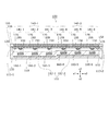
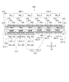
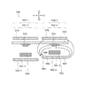
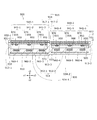
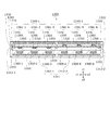
- FIG. 1 is a cross-sectional view of the current sensor 100 in a cross section parallel to the zx plane of the present embodiment.
- the y1 direction is perpendicular to the cross section shown in FIG.
- the y2 direction is a direction perpendicular to the cross section shown in FIG.
- the current sensor 100 includes a first housing 110 made of resin, a second housing 115 made of resin, a substrate 130 made of an insulating material mounted on the second housing 115, and the substrate 130 as the second housing 115. And a large current unit group 140-1 and a small current unit group 140-2 that are mounted on the first housing 110 and the second housing 115 and measure an induced magnetic field.
- the thickness in the z direction is substantially constant at any position. That is, the thickness in the z direction is substantially constant for the entire first facing portion 111.
- the first facing portion 111 may include a plurality of first sub facing portions 112 other than two.
- the first casing 110 includes a first support portion 113-1 extending in the z1 direction from the x1 side end portion of the first facing portion 111, and a second support portion 11x extending from the x2 side end portion of the first facing portion 111 in the z1 direction. And a support portion 113-2.
- the first housing 110 extends over a predetermined length in the y direction with the cross section shown in FIG.
- the second housing 115 includes a second facing portion 116.
- the entire second housing 115 is the second facing portion 116.
- the second housing 115 may include other components.
- the second facing portion 116 has a substantially flat plate shape having two surfaces substantially parallel to the xy plane and extending substantially parallel to the xy plane. The thickness of the second facing portion 116 in the z direction is substantially constant at any position.
- the x1 side end portion of the second facing portion 116 is fixed to the z1 side end portion of the first support portion 113-1.
- the x2 side end portion of the second facing portion 116 is fixed to the z1 side end portion of the second support portion 113-2.
- the first facing portion 111 and the second facing portion 116 are positioned to partially face each other in the z direction. A space exists between the first facing portion 111 and the second facing portion 116.
- the second housing 115 extends over a predetermined length in the y direction with the cross section shown in FIG.
- the substrate 130 is located between the first facing portion 111 and the second facing portion 116 in the z direction.
- the substrate 130 is located between the first support portion 113-1 and the second support portion 113-2 in the x direction.
- the substrate 130 is fixed to the second facing portion 116 by a plurality of fixing members 133.
- the substrate 130 has a substantially flat plate shape that extends substantially parallel to the xy plane.
- the thickness of the substrate 130 in the z direction is substantially constant.
- the substrate 130 has a first mounting surface 131 on the first facing portion 111 side and a second mounting surface 132 on the second facing portion 116 side.
- the first mounting surface 131 and the second mounting surface 132 are both substantially parallel to the xy plane.
- the substrate 130 is fixed to the other part of the second casing 115 or the first casing 110. That is, the substrate 130 is preferably fixed to at least one of the first housing 110 and the second housing 115. The substrate 130 spreads over a predetermined length in the y direction with the cross section shown in FIG.
- the large current unit group 140-1 and the small current unit group 140-2 (hereinafter sometimes referred to as the unit group 140 without distinction) are arranged adjacent to each other in the x direction (also referred to as the second direction).
- the large current unit group 140-1 measures a larger current than the small current unit group 140-2.
- the current sensor 100 may include three or more unit groups 140.
- the unit group 140 that measures a relatively large current among the adjacent unit groups 140 corresponds to the large current unit group 140-1, and the relative The unit group 140 that measures a small current corresponds to the small current unit group 140-2.
- the direction in which the two unit groups 140 are arranged may be another direction that intersects the z direction.
- Each of the two first sub-opposing portions 112 corresponds to a different unit group 140. That is, the left first sub-opposing portion 112-1 corresponds to the large current unit group 140-1. That is, as will be described later, a component that measures a relatively large current is located in the left first sub-opposing portion 112-1.
- the right first sub-opposing portion 112-2 corresponds to the small current unit group 140-2. That is, as will be described later, a component for measuring a relatively small current is located in the right first sub-opposing portion 112-2.
- the large current unit group 140-1 includes a first measurement unit 141-1 to a third measurement unit 141-3 arranged from the x1 side to the x2 side.
- the small current unit group 140-2 includes the fourth measurement unit 141-4 to the sixth measurement unit 141-6 arranged from the x1 side to the x2 side.
- the first measurement unit 141-1 to the sixth measurement unit 141-6 may be referred to as the measurement unit 141 without being distinguished from each other.
- each of the plurality of unit groups 140 may include two or less or four or more measurement units 141.
- each of the plurality of unit groups 140 includes the same number of measurement units 141, but in another example, each of the plurality of unit groups 140 may include a different number of measurement units 141.
- the current path 150 is made of metal and is integrally formed in the first facing portion 111.
- the cross section of the current path 150 is a substantially rectangular shape having two sides parallel to the x direction and two sides parallel to the z direction.
- the current path 150 extends over a predetermined length in the y direction with the cross section shown in FIG.
- the current path 150 extends to the outside of the first housing 110 and allows a current supplied from the outside to flow in the y direction.
- the current paths 150 have substantially the same shape within a predetermined length range in the y direction.
- the current path 150 included in each of the two unit groups 140 is located in the corresponding first sub-facing portion 112.
- the three current paths 150 included in the large current unit group 140-1 are located in the left first sub-opposing portion 112-1, and are on the z1 side surface of the left first sub-opposing portion 112-1 in the z direction. Is substantially constant, and the distance from the z2 side surface of the left first sub-facing portion 112-1 in the z direction is substantially constant.
- the three current paths 150 included in the large current unit group 140-1 are arranged at equal intervals in the x direction along substantially the same plane parallel to the xy plane.
- the three current paths 150 included in the small current unit group 140-2 are located in the right first sub-opposing portion 112-2 and extend from the z1 side surface of the right first sub-facing portion 112-2 in the z direction. The distance is substantially constant, and the distance from the z2 side surface of the right first sub-facing portion 112-2 in the z direction is substantially constant.
- the three current paths 150 included in the small current unit group 140-2 are arranged at equal intervals in the x direction along substantially the same plane parallel to the xy plane.
- the intervals in the x direction of the six current paths 150 are substantially the same.
- the three current paths 150 included in the small current unit group 140-2 are shifted in the z1 direction from the three current paths 150 included in the large current unit group 140-1.
- the deviation amount of the current path 150 in the z direction is smaller than the thickness of the current path 150 in the z direction, and is substantially the same as the predetermined deviation amount of the first sub-facing portion 112.
- All the magnetoelectric conversion elements 155 are mounted on one substantially flat substrate 130.
- the magnetoelectric conversion element 155 is mounted on the first mounting surface 131 of the substrate 130.
- the magnetoelectric conversion element 155 is, for example, a magnetoresistive effect element or a Hall element.
- the magnetoelectric conversion element 155 measures an induced magnetic field generated by a current flowing through the current path 150 in the common measurement unit 141.
- the magnetoelectric conversion element 155 sets the x direction as the sensitivity direction. That is, the magnetoelectric conversion element 155 detects the x-direction component in the magnetoelectric conversion element 155 from the induced magnetic field generated around the current path 150.
- the first magnetic shield 160 is made of a magnetic material and is integrally formed in the first facing portion 111.
- the cross section of the first magnetic shield 160 is a substantially rectangular shape having two sides parallel to the x direction and two sides parallel to the z direction.
- the first magnetic shield 160 extends over a predetermined length in the y direction with the cross section shown in FIG.
- the first magnetic shield 160 as a whole is a substantially rectangular parallelepiped having two surfaces substantially parallel to the xy plane, two surfaces substantially parallel to the yz plane, and two surfaces substantially parallel to the zx plane.
- the first magnetic shield 160 has a plate shape that extends along a plane substantially orthogonal to the z direction. All the first magnetic shields 160 have substantially the same shape.
- the first magnetic shield 160 included in each of the two unit groups 140 is located in the corresponding first sub-facing portion 112.
- the three first magnetic shields 160 included in the large current unit group 140-1 are located in the left first sub-opposing portion 112-1, and from the surface on the z1 side of the left first sub-opposing portion 112-1. Is substantially constant, and the distance from the z2 side surface of the left first sub-facing portion 112-1 is substantially constant.
- the three first magnetic shields 160 included in the large current unit group 140-1 extend along substantially the same plane parallel to the xy plane, and are arranged at equal intervals in the x direction.
- the three first magnetic shields 160 included in the small current unit group 140-2 are located in the right first sub-facing portion 112-2, and the distance from the z1 side surface of the right first sub-facing portion 112-2. Is substantially constant, and the distance from the z2 side surface of the right first sub-facing portion 112-2 is substantially constant.
- the three first magnetic shields 160 included in the small current unit group 140-2 extend along substantially the same plane parallel to the xy plane, and are arranged at equal intervals in the x direction.
- the intervals in the x direction of the six first magnetic shields 160 are substantially the same.
- the three first magnetic shields 160 included in the small current unit group 140-2 are shifted in the z1 direction from the three first magnetic shields 160 included in the large current unit group 140-1.
- the shift amount of the first magnetic shield 160 in the z direction is substantially the same as the thickness of the first magnetic shield 160 in the z direction, and is approximately the same as the predetermined shift amount of the first sub-facing portion 112.
- the predetermined shift amount of the first sub-facing portion 112, the shift amount of the first magnetic shield 160, and the shift amount of the current path 150 are not limited to the amounts given in this embodiment.
- the second magnetic shield 170 is made of a magnetic material and is integrally formed in the second facing portion 116.
- the cross section of the second magnetic shield 170 is a substantially rectangular shape having two sides parallel to the x direction and two sides parallel to the z direction.
- the second magnetic shield 170 extends over a predetermined length in the y direction with the cross section shown in FIG.
- the second magnetic shield 170 as a whole is a substantially rectangular parallelepiped having two surfaces substantially parallel to the xy plane, two surfaces substantially parallel to the yz plane, and two surfaces substantially parallel to the zx plane.
- the second magnetic shield 170 has a plate shape that extends along a plane substantially orthogonal to the z direction. All the second magnetic shields 170 have substantially the same shape.
- the six second magnetic shields 170 extend along substantially the same plane parallel to the xy plane, and are arranged at equal intervals in the x direction.
- the second magnetic shield 170 is located approximately at the center of the second facing portion 116 in the z direction.
- the second magnetic shield 170 has substantially the same shape as the first magnetic shield 160.
- the current path 150 is located between the first magnetic shield 160 and the second magnetic shield 170.
- the magnetoelectric conversion element 155 is mounted on the substrate 130 between the current path 150 and the second magnetic shield 170.
- the current path 150, the magnetoelectric conversion element 155, the first magnetic shield 160, and the second magnetic shield 170 are in overlapping positions when viewed from the z direction.
- the centers of the current path 150, the magnetoelectric transducer 155, the first magnetic shield 160, and the second magnetic shield 170 in the x direction are generally positioned in a straight line parallel to the z direction.
- the second magnetic shield 170 is at a position obtained by translating the first magnetic shield 160 in the z1 direction.
- the width of the magnetoelectric conversion element 155 in the x direction is smaller than the width of the current path 150 in the x direction.
- the widths of the first magnetic shield 160 and the second magnetic shield 170 in the x direction are both larger than the width of the current path 150 in the x direction.
- the centers in the y direction of the magnetoelectric transducer 155, the first magnetic shield 160, and the second magnetic shield 170 are generally positioned in a straight line parallel to the z direction.
- the widths in the y direction of the first magnetic shield 160 and the second magnetic shield 170 are both larger than the width in the y direction of the magnetoelectric transducer 155.
- the region of the current path 150 that extends linearly in the y direction is longer than the width of the magnetoelectric conversion element 155 in the y direction.
- the current path 150 and the first magnetic shield 160 included in the common measurement unit 141 are positioned a first distance apart in the z direction.
- all the first distances are substantially the same. That is, the first distance of the large current unit group 140-1 and the first distance of the small current unit group 140-2 are substantially the same.
- the current path 150 and the magnetoelectric conversion element 155 included in the common measurement unit 141 are located a second distance apart in the z direction.
- the second distance is substantially the same. That is, all the second distances in the large current unit group 140-1 are substantially the same. All the second distances in the small current unit group 140-2 are substantially the same. The second distance is different for each unit group 140. Specifically, the second distance of the small current unit group 140-2 is smaller than the second distance of the large current unit group 140-1.
- the magnetoelectric conversion element 155 and the second magnetic shield 170 included in the common measurement unit 141 are located a third distance apart in the z direction. In all measurement units 141, the third distance is shorter than the second distance. In all the measurement units 141, the third distance is substantially the same.
- the current path 150 and the second magnetic shield 170 included in the common measurement unit 141 are located a fourth distance apart in the first direction.
- the fourth distance in the large current unit group 140-1 is larger than the fourth distance in the small current unit group 140-2.
- the first magnetic shield 160 and the second magnetic shield 170 included in the common measurement unit 141 are located at a distance of a fifth distance in the first direction.
- the fifth distance in the large current unit group 140-1 is larger than the fifth distance in the small current unit group 140-2.
- All the magnetoelectric transducers 155 are located on the same plane substantially parallel to the xy plane. Further, the three current paths 150 included in the small current unit group 140-2 are closer to the magnetoelectric conversion element 155 than the three current paths 150 included in the large current unit group 140-1. Therefore, a relatively small current can be measured with high accuracy in the small current unit group 140-2. Furthermore, the magnetoelectric transducer 155 of the fourth measurement unit 141-4 is located farther from the current path 150 of the third measurement unit 141-3 than when all the current paths 150 are located on the same plane. As a result, the magnetoelectric conversion element 155 of the fourth measurement unit 141-4 is less susceptible to noise from the current path 150 of the third measurement unit 141-3.
- the first resin housing 110 including the first facing portion 111
- the second resin housing 115 including the second facing portion 116
- a substrate 130 mounted on at least one of the body 115 and a plurality of unit groups 140 mounted on the first housing 110 and the second housing 115 and measuring an induced magnetic field, and the first facing portion 111.
- the second facing portion 116 are opposed to each other in the first direction
- the plurality of unit groups 140 are arranged in a second direction intersecting the first direction
- each of the plurality of unit groups 140 is in the second direction.
- Each of the one or more measurement units 141 is integrally formed with the first magnetic shield 160 integrally formed with the first facing portion 111 and the second facing portion 116.
- the second magnetic shield 170 and the first magnetic shield A current path 150 formed integrally with the first facing portion 111 between the magnetic field 160 and the second magnetic shield 170, and a magnetoelectric conversion element 155 for measuring an induced magnetic field generated by a current flowing through the current path 150,
- the magnetoelectric conversion element 155 is mounted on the substrate 130 between the current path 150 and the second magnetic shield 170 in the first direction, and the current path 150 and the first magnetic shield 160 included in the common measurement unit 141 are The first distance in one direction is far away, and in all the unit groups 140, all the first distances are substantially the same, and the current path 150 and the magnetoelectric transducer 155 included in the common measurement unit 141 are The second distance is substantially the same in all the measurement units 141 included in the common unit group 140 that are located at a distance of the second distance in one direction.
- the second distance is different for each unit group 140, the thickness of the first facing portion 111 in the first direction is substantially constant, and the thickness of the second facing portion 116 in the first direction is substantially constant. So it is easy to mold resin.
- the thickness of the first facing portion 111, the thickness of the second facing portion 116, and the first distance are substantially constant, so that the resin in the mold is manufactured at the time of manufacture. Is easy to flow. As a result, it is possible to provide the current sensor 100 capable of easily and integrally manufacturing the plurality of measurement units 141 even when the positional relationship between the components of the plurality of measurement units 141 that measure the induced magnetic field is not constant.
- the magnetoelectric conversion element 155 and the second magnetic shield 170 included in the common measurement unit 141 are located a third distance apart in the first direction, and the third measurement unit 141 includes the third Since the distance is shorter than the second distance and the third distance is substantially the same in all the measurement units 141, the measurement accuracy can be improved compared to other arrangements.
- the first facing portion 111 includes a plurality of first sub-facing portions 112 that are integrally formed with each other, and each of the plurality of first sub-facing portions 112 has a substantially flat plate shape, and the plurality of first sub-facing portions 112 The current paths included in each of the plurality of unit groups 140, each of the plurality of first sub-opposing portions 112 corresponding to one different unit group 140. Since the 150 and the first magnetic shield 160 are located in the corresponding first sub-facing portions 112, the first housing 110 can be easily manufactured.
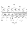
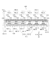
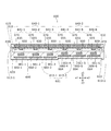
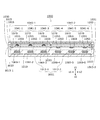
- FIG. 2 is a cross-sectional view of the current sensor 200 of the present embodiment in a cross section parallel to the zx plane.
- the difference between the current sensor 100 of the first embodiment (FIG. 1) and the current sensor 200 of the present embodiment will be mainly described.
- the hundreds of each component is represented by 1.
- the hundreds of each component is represented. It is represented by 2. Unless otherwise specified, components that differ only in the hundreds represent similar components.
- the first magnetic shields 260 of the first measurement unit 241-1 to the sixth measurement unit 241-6 are respectively arranged in order from the plate-like portion 261-1 to the plate-like portion 261-6 (hereinafter referred to as plate-like without distinction). Part 261).
- Each of the plate-like portions 261 has the same shape as the first magnetic shield 160 of the first embodiment (FIG. 1). That is, all the first magnetic shields 260 include the plate-like portion 261 that extends along a plane substantially orthogonal to the z direction. All the plate-like portions 261 included in the large current unit group 240-1 spread along substantially the same plane. All the plate-like portions 261 included in the small current unit group 240-2 spread along substantially the same plane.
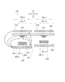
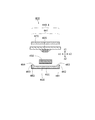
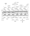
- FIG. 3 is a partially enlarged cross-sectional view of the current sensor 200 of the present embodiment in the vicinity of the third measurement unit 241-3 and the fourth measurement unit 241-4 shown in FIG.
- the first housing 210 and the second housing 215 are omitted.
- the plate-like portion 261-3 of the third measurement unit 241-3 included in the large current unit group 240-1 is close to the small current unit group 240-2 in the x direction.
- a second edge 282 far from the small current unit group 240-2 in the x direction.
- the first magnetic shield 260-3 of the third measurement unit 241-3 includes a first large current protrusion 262 extending from the first edge 281 toward the second facing portion 216 (FIG. 2).
- the first large current protrusion 262 is a substantially rectangular shape having two sides substantially parallel to the x direction and two sides substantially parallel to the z direction, and the entire plate-like portion 261 is arranged in the y direction. It extends along.
- a first tip 283 on the second facing portion 216 (FIG. 2) side ie, z1 side
- One surface 285 of the portion 216 (FIG. 2) side that is, the z1 side
- the magnetic flux generated by the current flowing through the current path 250 of the third measurement unit 241-3 of the present embodiment is further schematically shown by arrows.
- the magnetic flux passes through the first magnetic shield 260-3 from the second edge 282 in the x2 direction, passes through the first edge 281 of the plate-like part 261-3, and the first large current. Head toward the protrusion 262.
- a part of the magnetic flux emitted from the first large current protrusion 262 in the z1 direction passes between the current path 250 of the third measurement unit 241-3 and the magnetoelectric transducer 255, and passes through the second Return to edge 282.
- a part of the magnetic flux emitted from the first large current protrusion 262 in the z1 direction passes through the magnetoelectric conversion element 255 of the third measurement unit 241-3 in the x1 direction and returns to the second edge 282.
- a part of the magnetic flux emitted in the z1 direction from the first large current protrusion 262 enters the second magnetic shield 270 from the vicinity of the end of the second magnetic shield 270 of the third measurement unit 241-3 on the x2 side, and enters the second magnetic shield 270. It passes through 270 in the x1 direction and returns to the second edge 282 from the x1 side end of the second magnetic shield 270.
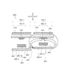
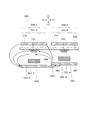
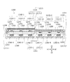
- FIG. 4 is a partially enlarged sectional view of the current sensor 200 of the present embodiment in the same range as FIG.
- the magnetic flux generated by the current flowing through the current path 250 of the fourth measurement unit 241-4 of the present embodiment is further schematically shown by arrows.
- the magnetic flux goes from the x1 side end of the first magnetic shield 260-4 in the x2 direction and exits from the x2 side end of the first magnetic shield 260-4 in the x2 direction.
- a part of the magnetic flux emitted from the x2 side end of the first magnetic shield 260-4 of the fourth measurement unit 241-4 is converted into the current path 250 and the magnetoelectric conversion of the fourth measurement unit 241-4.
- the element 255 Part of the magnetic flux emitted from the end on the x2 side of the first magnetic shield 260-4 passes through the magnetoelectric conversion element 255 of the fourth measurement unit 241-4 in the x1 direction, and is on the x1 side of the first magnetic shield 260-4. Return to the edge.
- FIG. 5 is a partially enlarged sectional view of a current sensor 2000 of a comparative example in the same range as FIG.
- the hundreds of each component is represented by 2.
- the current sensor 2000 of the comparative example shown in FIG. It is represented by Unless otherwise specified, components that differ by only a hundred or more represent similar components.
- the first magnetic shield 2060-3 of the third measurement unit 2041-3 in the comparative example shown in FIG. 5 does not include the first large current protrusion 262 (FIG. 3).
- the magnetic flux generated by the current flowing through the current path 2050 of the third measurement unit 2041-3 of the comparative example is further schematically shown by arrows.
- the magnetic flux emitted from the x2 side end of the first magnetic shield 2060-3 in the third measurement unit 2041-3 is fourth from the surface on the z2 side of the first magnetic shield 2060-4 in the fourth measurement unit 2041-4.
- the first magnetic shield 2060-4 of the measurement unit 2041-4 is entered.
- the magnetic flux that has entered the first magnetic shield 2060-4 of the fourth measurement unit 2041-4 exits in the z1 direction from the entire surface on the z1 side of the first magnetic shield 2060-4 in the fourth measurement unit 2041-4.
- a part of the magnetic flux emitted from the first magnetic shield 2060-4 of the fourth measurement unit 2041-4 is the end portion on the x2 side of the second magnetic shield 2070 in the third measurement unit 2041-3. And the other part enters the second magnetic shield 2070 of the fourth measuring unit 2041-4.
- the magnetic flux that has entered the second magnetic shield 2070 of the fourth measurement unit 2041-4 is transmitted from the x1 side end of the second magnetic shield 2070 of the fourth measurement unit 2041-4 to the second magnetic shield of the third measurement unit 2041-3. Enter the end of the shield 2070 on the x2 side.
- the magnetic flux that has entered the second magnetic shield 2070 of the third measurement unit 2041-3 exits in the x1 direction from the x1 side end portion of the second magnetic shield 2070 of the third measurement unit 2041-3, and the third measurement unit 2041- 3 returns to the x1-side end of the first magnetic shield 2060-3.
- the magnetic flux generated by the current flowing through the current path 2050 of the fourth measurement unit 2041-4 of the comparative example is the same as that of the present embodiment shown in FIG.
- the magnetic flux generated by the current path 2050 of the third measurement unit 2041-3 spreads to the fourth measurement unit 2041-4. Therefore, the sensitivity of the third measurement unit 2041-3 in the magnetoelectric conversion element 2055 is lowered.
- the magnetic flux generated by the current path 250 of the third measurement unit 241-3 is transferred to the fourth measurement unit 241-4. Since it is difficult to spread, the sensitivity in the magnetoelectric transducer 255 of the third measurement unit 241-3 can be maintained.
- the magnetic field in the fourth measurement unit 241-4 does not change greatly. Therefore, regardless of the presence or absence of the first large current protrusion 262, the difference from the sensitivity between the measurement units 241 in the small current unit group 240-2 can be suppressed small.
- the first tip 283 of the first large current protrusion 262 is arranged in the small current unit group 240-2 in the z direction so as not to disturb the induced magnetic field that is the measurement target of the small current unit group 240-2 itself shown in FIG. It is preferable to be located at the same position as the one surface 285 of the plate-like portion 261 or at the z2 side from the one surface 285. Considering the balance between the sensitivity improvement in the large current unit group 240-1 and the sensitivity maintenance in the small current unit group 240-2, the first tip 283 of the first large current protrusion 262, the small current unit group 240-2, It is preferable that the one surface 285 of the plate-like portion 261 is located on substantially the same plane orthogonal to the z direction.
- one of the plurality of unit groups 240 is a large current unit group 240-1, and the other one of the plurality of unit groups 240 is induced by a smaller current than the large current unit group 240-1.
- a small current unit group 240-2 for measuring a magnetic field wherein the large current unit group 240-1 and the small current unit group 240-2 are adjacent to each other, and all the first magnetic shields 260 include the second direction.
- All plate-like portions 261 included in the large current unit group 240-1 including the plate-like portion 261 extending along the plane extend along substantially the same plane and all included in the small current unit group 240-2
- the plate-like portion 261 extends along substantially the same plane, and the current path 250 and the second magnetic shield 270 included in the common measurement unit 241 are separated by a fourth distance in the first direction.
- the fourth distance in the large current unit group 240-1 is larger than the fourth distance in the small current unit group 240-2, and the first magnetic shield 260 and the second magnetic shield 270 included in the common measurement unit 241.
- the fifth distance in the large current unit group 240-1 is greater than the fifth distance in the small current unit group 240-2, and the large current unit group 240- 1 includes a first edge portion 281 that is close to the small current unit group 240-2 in the second direction and a second edge portion 282 that is far from the small current unit group 240-2 in the second direction.
- the first magnetic shield 260 closest to the small current unit group 240-2.
- the first magnetic shield 260 closest to the small current unit group 240-2 in the large current unit group 240-1 and the large current unit group in the small current unit group 240-2 When viewed with the first magnetic shield 260 closest to 240-1, the first magnetic shield 260 of the large current unit group 240-1 is second opposite to the first magnetic shield 260 of the small current unit group 240-2. Located far from the part 216. Therefore, when there is no first large current protrusion 262, most of the induced magnetic field from the edge on the small current unit group 240-2 side of the plate-like portion 261 in the first magnetic shield 260 of the large current unit group 240-1 It diffuses to the first magnetic shield 260 of the small current unit group 240-2.
- the sensitivity of the measurement unit 241 closest to the small current unit group 240-2 in the large current unit group 240-1 decreases.
- most of the induced magnetic field is generated from the edge on the small current unit group 240-2 side of the plate-like portion 261 in the first magnetic shield 260 of the large current unit group 240-1. It is directed to the second facing portion 216 via the large current protrusion 262. As a result, unwanted diffusion of the induced magnetic field from the large current unit group 240-1 toward the small current unit group 240-2 can be prevented.
- the first tip 283 on the second facing portion 216 side of the first large current protrusion 262 in the first direction and the plate-like portion 261 in the first magnetic shield 260 of the small current unit group 240-2 Since the one surface 285 on the second facing portion 216 side is located on substantially the same plane orthogonal to the first direction, diffusion of the induced magnetic field from the large current unit group 240-1 toward the small current unit group 240-2 And diffusion of the induced magnetic field from the small current unit group 240-2 to the large current unit group 240-1 can be kept to a minimum, and between the large current unit group 240-1 and the small current unit group 240-2, The sensitivity in the measurement unit 241 adjacent to the boundary can be made equal to the sensitivity in the other measurement units 241.
- FIG. 6 is a cross-sectional view of the current sensor 300 of the present embodiment in a cross section parallel to the zx plane.
- FIG. 2 the hundreds of each component is represented by 2.
- the hundreds of each component is shown. It is represented by 3. Unless otherwise specified, components that differ only in the hundreds represent similar components.
- each of the first measurement unit 341-1 to the third measurement unit 341-3 includes a first large current protrusion 362.
- the shapes of all the first magnetic shields 360 included in the large current unit group 340-1 are substantially the same, the sensitivity between the measurement units 341 included in the large current unit group 340-1. Design that suppresses the difference is easy. Moreover, parts can be made common and manufacturing management cost can be suppressed.
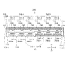
- FIG. 7 is a cross-sectional view of the current sensor 400 of the present embodiment in a cross section parallel to the zx plane.
- FIG. 6 the hundreds of each component is represented by 3.
- the hundreds of each component is represented. It is represented by 4. Unless otherwise specified, components that differ only in the hundreds represent similar components.
- FIG. 8 is a partially enlarged sectional view of one measurement unit 441 and the substrate 430 included in the large current unit group 440-1 shown in FIG.
- the first magnetic shield 460 of the large current unit group 440-1 includes the second large edge 482 to the second facing portion 416 in addition to the first large current protrusion 462 similar to that of the third embodiment.
- a second large current protrusion 463 extending toward (FIG. 7) is included. That is, each of the first magnetic shields 460 (FIG. 7) including the first large current protrusion 462 (FIG. 8) has the second large current protrusion 463 (FIG. 8).
- the second large current protrusion 463 has a substantially rectangular shape having two sides substantially parallel to the x direction and two sides substantially parallel to the z direction, and the entire plate-like portion 461 in the y direction. It extends along.
- the first magnetic shield 460 has a two-fold symmetrical shape that overlaps when rotated by 180 degrees around an axis extending in the z direction. That is, when the first large current protrusion 462 is rotated 180 degrees, it overlaps the second large current protrusion 463.
- the first magnetic shield 460 included in the first magnetic shield 460 is positioned on the substantially same plane perpendicular to the z direction.
- the distance between the current path 450 and the magnetoelectric conversion element 455 in the large current unit group 440-1 shown in FIG. 7 is the same as that of the small current unit group 440-2 to avoid saturation of the magnetoelectric conversion element 455. Generally, the distance is larger than the distance from the conversion element 455.
- the first magnetic shield 460 of the large current unit group 440-1 includes both the first large current protrusion 462 and the second large current protrusion 463, so that 2 Magnetic flux toward the magnetic shield 470 increases. As a result, the magnetic flux passing through the magnetoelectric conversion element 455 is reduced.
- the distance between the current path 450 and the magnetoelectric conversion element 455 in the large current unit group 440-1 is reduced.
- the distance between the current path 450 and the magnetoelectric conversion element 455 in the current unit group 440-2 can be made closer. As a result, it is possible to increase the strength of the first housing 410 by reducing the deviation between the left first sub-opposing portion 412-1 and the right first sub-opposing portion 412-2.
- each of the one or more first magnetic shields 460 including the first large current protrusion 462 extends from the second edge 482 toward the second opposing portion 416. Therefore, it is easy to align the direction of the first magnetic shield 460 by using both the first large current protrusion 462 and the second large current protrusion 463 during manufacturing, and the structure of the component supply portion of the manufacturing apparatus is simplified.
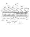
- FIG. 9 is a cross-sectional view of the current sensor 500 of the present embodiment in a cross section parallel to the zx plane.
- the difference between the current sensor 100 of the first embodiment (FIG. 1) and the current sensor 500 of the present embodiment will be mainly described.
- the hundreds of each component is represented by 1.
- the hundreds of each component is shown. It is represented by 5. Unless otherwise specified, components that differ only in the hundreds represent similar components.
- the first magnetic shields 560 of the first measurement unit 541-1 to the sixth measurement unit 541-6 are respectively arranged in order from the plate-like portion 561-1 to the plate-like portion 561-6 (hereinafter referred to as plate-like without distinction). Part 561).
- Each of the plate-like portions 561 has substantially the same shape as the first magnetic shield 160 of the first embodiment.
- All the first magnetic shields 560 include a plate-like portion 561 that extends along a plane substantially orthogonal to the z direction.
- All the plate-like portions 561 included in the large current unit group 540-1 spread along substantially the same plane. All the plate-like portions 561 included in the small current unit group 540-2 spread along substantially the same plane. However, the width in the x direction of the plate-like portion 561 included in the small current unit group 540-2 is slightly smaller than the width in the x direction of the plate-like portion 561 included in the large current unit group 540-1.
- FIG. 10 is a partially enlarged cross-sectional view of the current sensor 500 of the present embodiment in the vicinity of the third measurement unit 541-3 and the fourth measurement unit 541-4 shown in FIG.
- the first housing 510 and the second housing 515 are omitted.
- the plate-like portion 561-4 of the fourth measurement unit 541-4 included in the small current unit group 540-2 is close to the large current unit group 540-1 in the x direction.
- the first magnetic shield 560-4 of the fourth measurement unit 541-4 includes a first small current protrusion 564 extending from the first edge 586 toward the second facing portion 516 (FIG. 9).
- the first small current protrusion 564 extends in the direction between the z1 direction and the x1 direction in the cross section shown in FIG. In the cross section shown in FIG. 10, the first magnetic shield 560-4 and the first small current protrusion 564 form an obtuse angle.
- the width of the entire first magnetic shield 560-4 in the x direction is substantially the same as the width of the second magnetic shield 570 in the x direction.
- the first small current protrusion 564 extends along the entire plate-like portion 561 in the y direction.
- the first tip 588 on the second facing portion 516 (FIG. 9) side (ie, z1 side) of the first small current protrusion 564 in the z direction is , At a position far away from the second facing portion 516 (FIG. 9) from the center of the current path 550 in the z direction (ie, on the z2 side).
- FIG. 10 further schematically shows the magnetic flux generated by the current flowing in the current path 550 of the third measurement unit 541-3 of the present embodiment with arrows.
- the magnetic flux entering from the x1 side end of the first magnetic shield 560-3 of the third measurement unit 541-3 exits from the x2 side end of the first magnetic shield 560-3 in the x2 direction, and from the z2 side surface.
- the first magnetic shield 560-4 of the fourth measurement unit 541-4 is entered.
- the magnetic flux that has entered the first magnetic shield 560-4 of the fourth measurement unit 541-4 exits from the first small current protrusion 564 in the z1 direction.
- a part of the magnetic flux emitted from the first small current protrusion 564 passes between the current path 550 and the magnetoelectric transducer 555 in the third measurement unit 541-3, and passes through the third measurement unit 541. -3 returns to the x1 side end of the first magnetic shield 560-3.
- Part of the magnetic flux emitted from the first small current protrusion 564 passes through the magnetoelectric conversion element 555 in the x1 direction in the third measurement unit 541-3 and returns to the x1 side end of the first magnetic shield 560-3.
- FIG. 11 is a partially enlarged view of the current sensor 500 of the present embodiment in the same range as FIG.
- the magnetic flux generated by the current flowing in the current path 550 of the fourth measurement unit 541-4 of the present embodiment is further schematically shown by arrows.
- the magnetic flux travels in the x2 direction from the x1 end of the first magnetic shield 560-4 and exits in the x2 direction from the x2 end of the first magnetic shield 560-4.
- a part of the magnetic flux emitted from the first magnetic shield 560-4 passes between the current path 550 and the magnetoelectric transducer 555 and returns to the first small current protrusion 564.
- Part of the magnetic flux emitted from the first magnetic shield 560-4 passes through the magnetoelectric conversion element 555 in the x1 direction and returns to the first small current protrusion 564.
- Part of the magnetic flux emitted from the first magnetic shield 560-4 enters the second magnetic shield 570 from the x2 side end of the second magnetic shield 570, passes through the second magnetic shield 570 in the x1 direction, and passes through the second magnetic shield 570. It returns to the first small current protrusion 564 from the x1 side end of 570.
- the magnetic flux generated by the current path 2050 of the third measurement unit 2041-3 is Since it extends to the four measurement units 2041-4, the sensitivity of the third measurement unit 2041-3 in the magnetoelectric transducer 2055 decreases.
- the magnetic flux generated by the current path 550 of the third measurement unit 541-3 is applied to the fourth measurement unit 541-4. Since it is difficult to spread, the sensitivity in the magnetoelectric conversion element 555 of the third measurement unit 541-3 can be maintained.
- the magnetic field in the fourth measurement unit 541-4 does not change significantly. Therefore, regardless of the presence or absence of the first small current protrusion 564, the difference with the sensitivity between the measurement units 541 in the small current unit group 540-2 can be suppressed small.
- one of the plurality of unit groups 540 is a large current unit group 540-1
- the other one of the plurality of unit groups 540 is a small current unit group 540-2.
- the group 540-1 and the small current unit group 540-2 are adjacent to each other, and all the first magnetic shields 160 include plate-like portions 561 that extend along a plane including the second direction, and the large current unit group 540 -1 includes all the plate-like portions 561 extending along substantially the same plane, and all the plate-like portions 561 included in the small current unit group 540-2 extend along substantially the same plane, and are common.
- the current path 550 and the second magnetic shield 570 included in the measurement unit 541 are located at a distance of a fourth distance in the first direction, and the fourth distance in the large current unit group 540-1 is the small current unit.
- the first magnetic shield 560 and the second magnetic shield 570 which are larger than the fourth distance in the group G 540-2 and are included in the common measurement unit 541 are located at a distance of the fifth distance in the first direction, and have a large current.
- the fifth distance in the unit group 540-1 is larger than the fifth distance in the small current unit group 540-2, and the plate-like portion 561 included in the small current unit group 540-2 is connected to the large current unit group in the second direction.
- One or more first magnetic shields 560 including the first magnetic shield 560 closest to the high-current unit group 540-1 among the first current shields 560 are connected to the second pair from the first edge 586. Since having a first small current projection 564 extending toward the section 516, it is possible to prevent diffusion of unwanted induced magnetic field directed from the high current unit group 540-1 to the small current unit group 540-2.
- the first magnetic shield 560 closest to the small current unit group 540-2 in the large current unit group 540-1 and the large current unit group in the small current unit group 540-2 When viewed with the first magnetic shield 560 closest to 540-1, the first magnetic shield 560 of the large current unit group 540-1 is second opposite to the first magnetic shield 560 of the small current unit group 540-2. Located far from the part 516. Therefore, when there is no first small current protrusion 564, most of the induced magnetic field is generated from the edge on the small current unit group 540-2 side of the plate-like portion 561 in the first magnetic shield 560 of the large current unit group 540-1. It diffuses into the small current unit group 540-2.
- the sensitivity of the measurement unit 541 closest to the small current unit group 540-2 in the large current unit group 540-1 decreases.
- the first magnetic shield 560 of the small current unit group 540-2 is formed from the edge of the first magnetic shield 560 of the large current unit group 540-1 on the small current unit group 540-2 side.
- Most of the induced magnetic field diffused in the direction is directed to the second facing portion 516 via the first small current protrusion 564, and easily returns to the large current unit group 540-1 side.
- undesired diffusion of the induced magnetic field from the large current unit group 540-1 toward the small current unit group 540-2 can be prevented.
- the induced magnetic field to be measured by the small current unit group 540-2 is also concentrated on the first small current protrusion 564.
- the induced magnetic field to be measured in the small current unit group 540-2 is concentrated on the end of the first magnetic shield 560 regardless of the presence or absence of the first small current protrusion 564, the small current unit group 540-2.
- the sensitivity at is less affected by the presence or absence of the first small current protrusion 564.
- the protrusion amount of the first small current protrusion 564 is preferably about the first distance that is the distance between the current path 550 and the first magnetic shield 560.
- the first tip 588 on the second facing portion 516 side of the first small current protrusion 564 in the first direction is the current in the first direction. Since the first magnetic shield 560 and the first small current protrusion 564 form an obtuse angle at a position farther from the second opposing portion 516 than the center of the path 550, the small current due to the provision of the first small current protrusion 564 The influence of the sensitivity difference in the unit group 540-2 can be suppressed.
- FIG. 12 is a cross-sectional view of the current sensor 600 of the present embodiment in a cross section parallel to the zx plane.
- FIG. 9 the hundreds of each component is represented by 5.
- the hundreds of each component is represented. It is represented by 6. Unless otherwise specified, components that differ only in the hundreds represent similar components.
- all the first magnetic shields 660 included in the small current unit group 640-2 of the present embodiment are substantially the same. That is, all the first magnetic shields 660 included in the small current unit group 640-2 of the present embodiment are the first magnetic shields 560- included in the fourth measurement unit 541-4 of the fifth embodiment (FIG. 9). Same as 4. As shown in FIG. 12, all the first magnetic shields 660 included in the small current unit group 640-2 have the same first small current protrusions 664 as the first small current protrusions 564 of the fifth embodiment (FIG. 9). Including.
- the sensitivity between the measurement units 641 included in the small current unit group 640-2 since all the first magnetic shields 660 included in the small current unit group 640-2 have substantially the same shape, the sensitivity between the measurement units 641 included in the small current unit group 640-2. Design that suppresses the difference is easy. Moreover, parts can be made common and manufacturing management cost can be suppressed.
- FIG. 13 is a cross-sectional view of the current sensor 700 of the present embodiment in a cross section parallel to the zx plane.
- the difference between the current sensor 500 (FIG. 9) of the fifth embodiment and the current sensor 700 of the present embodiment will be mainly described.
- the hundreds of each component is represented by 5.
- the hundreds of each component is represented. 7.
- components that differ only in the hundreds represent similar components.
- the width in the x direction of the plate-like portion 761-4 in the fourth measurement unit 741-4 is slightly narrower than the plate-like portion 561-4 (FIG. 12) of the fifth embodiment.
- the first magnetic shield 760-4 has a two-fold symmetrical shape that overlaps when rotated by 180 degrees about an axis parallel to the z direction. That is, when the first small current protrusion 764 is rotated 180 degrees, it overlaps the second small current protrusion 765.
- the second tip 789 on the z1 side of the second small current protrusion 765 and the first tip 788 on the z1 side of the first small current protrusion 764 are located on the same plane parallel to the xy plane.
- all the first magnetic shields 760 included in the small current unit group 740-2 have substantially the same shape.
- the first magnetic shield 760-3 of the third measurement unit 741-3 has a shape obtained by rotating the first magnetic shield 760-4 of the fourth measurement unit 741-4 by 180 degrees about an axis parallel to the z direction. is there. That is, the shapes of the plate-like portion 761-3, the first large current protrusion 762, and the second large current protrusion 763 of the third measurement unit 741-3 are the plate-like portions 761- of the fourth measurement unit 741-4, respectively. 4 corresponds to the shapes of the first small current protrusion 764 and the second small current protrusion 765.
- the first large current protrusion 762 of the third measurement unit 741-3 in the present embodiment functions in the same manner as the first large current protrusion 262 in the second embodiment (FIG. 2). As shown in FIG. 13, the shapes of all the first magnetic shields 760 included in the large current unit group 740-1 are substantially the same.
- the first housing 810 includes a third support portion 813-3 extending in the z1 direction from between the left first sub-facing portion 812-1 and the right first sub-facing portion 812-2.
- the second facing portion 816 of the present embodiment is a left second sub-facing portion 817-1 and a right second sub-facing portion 817-2 (hereinafter, the second sub-facing portion without distinction). It may be called 817). In another example, the second facing portion 816 may include three or more second sub-facing portions 817.
- the right first sub-facing portion 912-2 of the present embodiment is displaced in the z1 direction to the same extent as the first embodiment with respect to the left first sub-facing portion 912-1. Further, the three current paths 950 included in the small current unit group 940-2 are shifted in the z1 direction to the same extent as the first embodiment with respect to the three current paths 950 included in the large current unit group 940-1. ing. The three first magnetic shields 960 included in the small current unit group 940-2 are in the z1 direction to the same degree as in the first embodiment with respect to the three first magnetic shields 960 included in the large current unit group 940-1. It is shifted to.
- the first housing 1110 includes a third support portion 1113-3 that extends in the z1 direction from between the left first sub-facing portion 1112-1 and the right first sub-facing portion 111-2.
- the third support portion 1113-3 partially penetrates the substrate 1130.
- the second facing portion 1116 of the present embodiment is a left second sub-facing portion 1117-1 and a right second sub-facing portion 1117-2 (hereinafter, the second sub-facing portion without distinction). 1117).
- the second facing portion 1116 may include three or more second sub-facing portions 1117.
- one of the plurality of unit groups 1140 is the large current unit group 1140-1, and the other one of the plurality of unit groups 1140 is the small current unit group 1140-2, and the common measurement
- the current path 1150 and the second magnetic shield 1170 included in the unit 1141 are located a fourth distance apart in the first direction, and the fourth distance in the large current unit group 1140-1 is the small current unit group 1140-2.
- the right second sub-opposing portion 1217-2 is at a position shifted in the z2 direction from the left second sub-facing portion 1217-1.
- the three second magnetic shields 1270 included in the small current unit group 1240-2 are shifted to the z2 side from the three second magnetic shields 1270 included in the large current unit group 1240-1.
- the distance in the z direction between the current path 1250 and the second magnetic shield 1270 included in the common measurement unit 1241 is referred to as a fourth distance.
- the fourth distance in the large current unit group 1240-1 is different from the fourth distance in the small current unit group 1240-2 and is larger than the fourth distance in the small current unit group 1240-2.
- all current paths 1250 are located on substantially the same plane
- all first magnetic shields 1260 are located on substantially the same plane
- the substrate 1230 is the first facing portion 1211.
- the first mounting surface 1231 on the side and the second mounting surface 1232 on the second facing portion 1216 side, and all the magnetoelectric conversion elements 1255 included in one or more unit groups 1240 are mounted on the first mounting surface 1231. Since all the magnetoelectric conversion elements 1255 included in the one or more other unit groups 1240 are mounted on the second mounting surface 1232, either the first mounting surface 1231 or the second mounting surface 1232 is magnetoelectrically mounted at the time of manufacture. Depending on whether the conversion element 1255 is mounted, the distance between the magnetoelectric conversion element 1255 and the current path 1250 can be changed, and manufacturing is easy.
- the sensitivity of each unit group 1240 can be increased. It may simply be adjusted.
- 1st magnetic shield (260, 360, 460, 560, 660, 760, 860, 960, 1060, 1160, 1260, 1360) 170 ... 2nd magnetic shield (270, 370, 470, 570, 670, 770, 870, 970, 1070, 1170, 1270, 1370) 261 ... Plate-shaped part (361, 461, 561, 661, 761) 262: First large current protrusion (362, 462, 762) 281 ... 1st edge (381, 481, 781) 282 ... 2nd edge (381, 481, 781) 283 ... 1st front-end
- tip part (383, 483, 783) 285 ... one side (385, 485) 463 ...
Landscapes
- Physics & Mathematics (AREA)
- General Physics & Mathematics (AREA)
- Measuring Instrument Details And Bridges, And Automatic Balancing Devices (AREA)
Abstract
複数のユニット群140の各々が、第2方向に並んだ1つ以上の測定ユニット141を含む。共に第1対向部111に一体成形された電流路150と第1磁気シールド160とが第1距離ぶん離れて位置し、すべてのユニット群140において、すべての第1距離が略同一である。電流路150と第2対向部116に一体成形された磁電変換素子155とが第2距離ぶん離れて位置し、共通のユニット群140に含まれるすべての測定ユニット141おいて、第2距離が略同一である。ユニット群140ごとに、第2距離が異なり、第1方向における第1対向部111の厚みが、略一定であり、第1方向における第2対向部116の厚みが、略一定である。
Description
本発明は、電流センサに関する。
従来、電流が流れる電流路と、電流路を流れる電流を測定する磁電変換素子と、電流路と磁電変換素子とを挟む磁性体で作られた磁気シールドとを備える電流センサが知られている。さらに、例えば、特許文献1と特許文献2と特許文献3とに開示されているように、電流路と磁気シールドとが、筐体に一体成形されている電流センサが知られている。
また、ハイブリッド車や電気自動車では、エンジンルーム内に、駆動用モーターのインバーター用の電流センサと、制動用発電機のインバーター用の電流センサとを設ける必要がある。用途が異なる場合、測定対象の電流の大きさが異なる場合がある。従来、大電流用の電流センサと小電流用のセンサは、別々に用意される。
しかしながら、エンジンルームなどの限られたスペースに測定対象の電流の大きさが異なる複数の電流センサを配置すると、スペースを有効に活用できないという不利益がある。また、電流路と磁電変換素子と1つ以上の磁気シールドとを構成要素に含む測定ユニットを考えるとき、測定対象の電流が大電流であるか小電流であるかに応じて、測定ユニットごとに構成要素の相互の位置関係が異なるため、簡単に一体化することはできず、仮に一体化したとしても製造が困難である。
本発明はかかる事情に鑑みてなされたものであり、その目的は、誘導磁界を測定する複数の測定ユニットの構成要素の位置関係が一定ではない場合でも、複数の測定ユニットを一体的に容易に製造できる電流センサを提供することにある。
本発明は、第1対向部を含む樹脂製の第1筐体と、第2対向部を含む樹脂製の第2筐体と、第1筐体と第2筐体との少なくとも一方に搭載された基板と、第1筐体と第2筐体とに搭載されて誘導磁界を測定する複数のユニット群と、を備え、第1対向部と第2対向部とが、第1方向において対向して位置し、複数のユニット群が、第1方向に交差する第2方向に並び、複数のユニット群の各々が、第2方向に並んだ1つ以上の測定ユニットを含み、1つ以上の測定ユニットの各々が、第1対向部に一体成形された第1磁気シールドと、第2対向部に一体成形された第2磁気シールドと、第1磁気シールドと第2磁気シールドとの間において第1対向部に一体成形された電流路と、電流路に流れる電流により発生する誘導磁界を測定する磁電変換素子と、を含み、磁電変換素子が、第1方向において電流路と第2磁気シールドとの間で基板に搭載され、共通の測定ユニットに含まれる電流路と第1磁気シールドとが、第1方向において第1距離ぶん離れて位置し、すべてのユニット群において、すべての第1距離が略同一であり、共通の測定ユニットに含まれる電流路と磁電変換素子とが、第1方向において第2距離ぶん離れて位置し、共通のユニット群に含まれるすべての測定ユニットおいて、第2距離が略同一であり、ユニット群ごとに、第2距離が異なり、第1方向における第1対向部の厚みが、略一定であり、第1方向における第2対向部の厚みが、略一定である、電流センサである。
この構成によれば、樹脂成形しやすい。ユニット群ごとに第2距離が異なる構造において、第1対向部の厚みと、第2対向部の厚みと、第1距離とが、それぞれ略一定であるので、製造時に型内で樹脂が流れやすい。その結果、誘導電流を測定する複数の測定ユニットの構成要素の位置関係が一定ではない場合でも、複数の測定ユニットを一体的に容易に製造できる電流センサを提供できる。
好適には本発明の電流センサにおいて、共通の測定ユニットに含まれる磁電変換素子と第2磁気シールドとが、第1方向において第3距離ぶん離れて位置し、すべての測定ユニットにおいて、第3距離が、第2距離より短く、すべての測定ユニットにおいて、第3距離が、略同一である。
この構成によれば、他の配置に比べて測定精度を高めることができる。
すべての第2磁気シールドが、略同一の平面上に位置し、すべての磁電変換素子が、1枚の略平面状の基板に搭載されており、第1対向部が、相互に一体成形された複数の第1サブ対向部を含み、複数の第1サブ対向部の各々が、略平板状であり、複数の第1サブ対向部が、相互に第1方向にずれた位置にあり、複数の第1サブ対向部の各々が、異なる1つのユニット群に対応し、複数のユニット群の各々に含まれる電流路と第1磁気シールドとが、対応する第1サブ対向部に位置する。
この構成によれば、すべての第2磁気シールドが、略同一の平面上に位置し、すべての磁電変換素子が、1枚の略平面状の基板に搭載されているので、第2筐体と基板とを容易に製造できる。さらに、第1対向部が、相互に一体成形された複数の第1サブ対向部を含み、複数の第1サブ対向部の各々が、略平板状であり、複数の第1サブ対向部が、相互に第1方向にずれた位置にあり、複数の第1サブ対向部の各々が、異なる1つのユニット群に対応し、複数のユニット群の各々に含まれる電流路と第1磁気シールドとが、対応する第1サブ対向部に位置するので、第1筐体を容易に製造することができる。
好適には本発明の電流センサにおいて、複数のユニット群の1つが、大電流ユニット群であり、複数のユニット群の他の1つが、大電流ユニット群よりも小さな電流による誘導磁界を測定する小電流ユニット群であり、大電流ユニット群と小電流ユニット群とが隣接しており、すべての第1磁気シールドが、第2方向を含む平面に沿って広がる板状部を含み、大電流ユニット群に含まれるすべての板状部が、略同一の平面に沿って広がり、小電流ユニット群に含まれるすべての板状部が、略同一の平面に沿って広がり、共通の測定ユニットに含まれる電流路と第2磁気シールドとが、第1方向において第4距離ぶん離れて位置し、大電流ユニット群における第4距離が、小電流ユニット群における第4距離よりも大きく、共通の測定ユニットに含まれる第1磁気シールドと第2磁気シールドとが、第1方向において第5距離ぶん離れて位置し、大電流ユニット群における第5距離が、小電流ユニット群における第5距離よりも大きく、大電流ユニット群に含まれる板状部が、第2方向において小電流ユニット群に近い第1縁部と、第2方向において小電流ユニット群から遠い第2縁部とをもち、大電流ユニット群に含まれるすべての第1磁気シールドのうち、小電流ユニット群に最も近い第1磁気シールドを含む1つ以上の第1磁気シールドが、第1縁部から第2対向部に向けて延びた第1大電流突起を含む。
この構成によれば、大電流ユニット群から小電流ユニット群に向かう誘導磁界の望まない拡散を防ぐことができる。
具体的に説明すると、第1方向において、大電流ユニット群内で小電流ユニット群に最も近い第1磁気シールドと、小電流ユニット群内で大電流ユニット群に最も近い第1磁気シールドとを見たとき、大電流ユニット群の第1磁気シールドが、小電流ユニット群の第1磁気シールドよりも第2対向部から遠くに位置する。そのため、第1大電流突起がない場合、大電流ユニット群の第1磁気シールドにおける板状部の小電流ユニット群側の縁部から、誘導磁界の大半が、小電流ユニット群の第1磁気シールドに拡散する。その結果、第1大電流突起がない場合、大電流ユニット群内で小電流ユニット群に最も近い測定ユニットの感度が低下する。第1大電流突起がある場合、誘導磁界の大半が、大電流ユニット群の第1磁気シールドにおける板状部の小電流ユニット群側の縁部から、第1大電流突起を介して、第2対向部に向けられる。その結果、大電流ユニット群から小電流ユニット群に向かう誘導磁界の望まない拡散を防ぐことができる。
好適には本発明の電流センサにおいて、第1方向における第1大電流突起の第2対向部側の先端部と、小電流ユニット群の第1磁気シールドにおける板状部の第2対向部側の一面とが、第1方向に直交する略同一の平面上に位置する。
この構成によれば、大電流ユニット群から小電流ユニット群に向かう誘導磁界の拡散と、小電流ユニット群から大電流ユニット群に向かう誘導磁界の拡散とを最小限度に留めることができ、大電流ユニット群と小電流ユニット群との境界に隣接する測定ユニットにおける感度を、他の測定ユニットにおける感度と同等にできる。
好適には本発明の電流センサにおいて、大電流ユニット群に含まれるすべての第1磁気シールドの形状が、略同一である。
この構成によれば、大電流ユニット群に含まれる測定ユニット間の感度差を抑えた設計が容易となる。また、部品を共通化して、製造管理コストを抑制できる。
好適には本発明の電流センサにおいて、第1大電流突起を含む1つ以上の第1磁気シールドの各々が、第2縁部から第2対向部に向けて延びた第2大電流突起をもつ。
この構成によれば、製造時に第1大電流突起と第2大電流突起との両方とを利用して、第1磁気シールドの向きを揃えやすくなり、製造装置の部品供給部分の構造を簡略化できる。
好適には本発明の電流センサにおいて、複数のユニット群の1つが、大電流ユニット群であり、複数のユニット群の他の1つが、小電流ユニット群であり、大電流ユニット群と小電流ユニット群とが隣接しており、すべての第1磁気シールドが、第2方向を含む平面に沿って広がる板状部を含み、大電流ユニット群に含まれるすべての板状部が、略同一の平面に沿って広がり、小電流ユニット群に含まれるすべての板状部が、略同一の平面に沿って広がり、共通の測定ユニットに含まれる電流路と第2磁気シールドとが、第1方向において第4距離ぶん離れて位置し、大電流ユニット群における第4距離が、小電流ユニット群における第4距離よりも大きく、共通の測定ユニットに含まれる第1磁気シールドと第2磁気シールドとが、第1方向において第5距離ぶん離れて位置し、大電流ユニット群における第5距離が、小電流ユニット群における第5距離よりも大きく、小電流ユニット群に含まれる板状部が、第2方向において大電流ユニット群に近い第1縁部と、第2方向において大電流ユニット群から遠い第2縁部とをもち、小電流ユニット群に含まれるすべての第1磁気シールドのうち、大電流ユニット群に最も近い第1磁気シールドを含む1つ以上の第1磁気シールドが、第1縁部から第2対向部に向けて延びた第1小電流突起をもつ。
この構成によれば、大電流ユニット群から小電流ユニット群に向かう誘導磁界の望まない拡散を防ぐことができる。
具体的に説明すると、第1方向において、大電流ユニット群内で小電流ユニット群に最も近い第1磁気シールドと、小電流ユニット群内で大電流ユニット群に最も近い第1磁気シールドとを見たとき、大電流ユニット群の第1磁気シールドが、小電流ユニット群の第1磁気シールドよりも第2対向部から遠くに位置する。そのため、第1小電流突起がない場合、大電流ユニット群の第1磁気シールドにおける板状部の小電流ユニット群側の縁部から、誘導磁界の大半が、小電流ユニット群に拡散する。その結果、第1小電流突起がない場合、大電流ユニット群内で小電流ユニット群に最も近い測定ユニットの感度が低下する。第1小電流突起がある場合、大電流ユニット群の第1磁気シールドの小電流ユニット群側の縁部から、小電流ユニット群の第1磁気シールドに拡散した誘導磁界の大半が、第1小電流突起を介して、第2対向部に向けられ、大電流ユニット群側に戻りやすくなる。その結果、大電流ユニット群から小電流ユニット群に向かう誘導磁界の望まない拡散を防ぐことができる。
なお、小電流ユニット群で測定対象とする誘導磁界も第1小電流突起に集中する。しかし、小電流ユニット群で測定対象とする誘導磁界は、第1小電流突起の有無にかかわらず、第1磁気シールドの端部に集中するため、小電流ユニット群における感度は、第1小電流突起の有無により影響を受けにくい。ただし、小電流ユニット群に含まれる測定ユニット間の感度差を小さくするには、第1方向における第1小電流突起の突出量を第1距離程度に小さくすることが好ましい。
第1小電流突起を含む測定ユニットにおいて、第1方向における第1小電流突起の第2対向部側の先端部は、第1方向における電流路の中心より、第2対向部から遠い位置にあり、第1磁気シールドと第1小電流突起とが鈍角を形成する。
この構成によれば、第1小電流突起を設けたことによる小電流ユニット群における感度差の影響を抑えられる。
好適には本発明の電流センサにおいて、小電流ユニット群に含まれるすべての第1磁気シールドの形状が、略同一である。
この構成によれば、小電流ユニット群に含まれる測定ユニット間の感度差を抑えた設計が容易となる。また、部品を共通化して、製造管理コストを抑制できる。
好適には本発明の電流センサにおいて、第1小電流突起を含む1つ以上の第1磁気シールドの各々が、第2縁部から第2対向部に向けて延びた第2小電流突起をもつ。
この構成によれば、製造時に第1小電流突起と第2小電流突起との両方とを利用して、第1磁気シールドの向きを揃えやすくなり、製造装置の部品供給部分の構造を簡略化できる。
好適には本発明の電流センサにおいて、すべての第1磁気シールドの形状が、略同一である。
この構成によれば、部品が共通化され、製造管理コストを抑制できる。
好適には本発明の電流センサにおいて、複数のユニット群の各々が、同数の測定ユニットを含み、第2対向部が、略同一形状の複数の第2サブ対向部を含み、基板が、略同一形状の複数のサブ基板を含み、複数のユニット群の各々に、第2サブ対向部とサブ基板とが対応し、同じユニット群に対応する第2サブ対向部とサブ基板とが、相互に固定されており、各第2サブ対向部が、対応するユニット群に含まれるすべての第2磁気シールドを搭載し、各サブ基板が、対応するユニット群に含まれるすべての磁電変換素子を搭載する。
この構成によれば、第2サブ対向部とサブ基板とを組み立てた部品を、複数のユニット群で共通化して、製造コストを減らせる。
好適には本発明の電流センサにおいて、すべての電流路が略同一の平面上に位置し、すべての第1磁気シールドが略同一の平面上に位置する。
この構成によれば、第1対向部の形状が簡略化され、樹脂成形しやすい。
好適には本発明の電流センサにおいて、すべての電流路が、略同一の平面上に位置し、すべての第1磁気シールドが、略同一の平面上に位置し、基板が、第1対向部側の第1搭載面と第2対向部側の第2搭載面とをもち、1つ以上のユニット群に含まれるすべての磁電変換素子が、第1搭載面に搭載され、他の1つ以上のユニット群に含まれるすべての磁電変換素子が、第2搭載面に搭載される。
この構成によれば、製造時に第1搭載面と第2搭載面とのいずれに磁電変換素子を搭載するかによって、磁電変換素子と電流路との距離を変えることができ、製造が容易である。
好適には本発明の電流センサにおいて、すべての第2磁気シールドが、略同一の平面上に位置する。
この構成によれば、すべての第2磁気シールドが、略同一の平面上に位置するので、第1対向部に加えて、第2対向部も容易に製造することができる。さらに、第1搭載面と第2搭載面とのいずれに磁電変換素子を搭載するかによって、磁電変換素子と電流路との距離を変えることができるので、第1搭載面と第2搭載面との何れか一方に磁電変換素子を搭載する場合に比べて、一部のユニット群において、第2磁気シールドと磁電変換素子との距離が近すぎること、または遠すぎることとを防止できる。その結果、各ユニット群に必要とされる感度を達成しやすい。
例えば、大電流を測定するユニット群では、磁電変換素子を第2搭載面に搭載することで、磁電変換素子を第2磁気シールドに近づけることで、あえて感度を抑えることができる。一方、小電流を測定するユニット群では、磁電変換素子を第1搭載面に搭載することで、磁電変換素子を第2磁気シールドから遠ざけ、感度を高めることができる。
好適には本発明の電流センサにおいて、複数のユニット群の1つが、大電流ユニット群であり、複数のユニット群の他の1つが、小電流ユニット群であり、共通の測定ユニットに含まれる電流路と第2磁気シールドとが、第1方向において第4距離ぶん離れて位置し、大電流ユニット群における第4距離が、小電流ユニット群における第4距離と異なる。
この構成によれば、第1搭載面と第2搭載面とのいずれに磁電変換素子を搭載するかによって磁電変換素子と電流路との距離を変える場合において、さらに、磁電変換素子と第2磁気シールドとの距離を調節することにより、ユニット群ごとの感度を簡単に調節することができる。
好適には本発明の電流センサにおいて、共通の測定ユニットに含まれる磁電変換素子と第2磁気シールドとが、第1方向において第3距離ぶん離れて位置し、すべての測定ユニットにおいて、第3距離が、略同一である。
この構成によれば、他の配置に比べて測定精度を高めることができる。
好適には本発明の電流センサにおいて、複数のユニット群の1つが、大電流ユニット群であり、複数のユニット群の他の1つが、小電流ユニット群であり、共通の測定ユニットに含まれる第2磁気シールドと磁電変換素子とが、第1方向において第3距離ぶん離れて位置し、大電流ユニット群における第3距離が、小電流ユニット群における第3距離より小さい。
この構成によれば、小電流ユニット群における感度を、大電流ユニット群における感度よりも高くすることができる。
好適には本発明の電流センサにおいて、複数のユニット群の1つが、大電流ユニット群であり、複数のユニット群の他の1つが、小電流ユニット群であり、共通の測定ユニットに含まれる第2磁気シールドと磁電変換素子とが、第1方向において第3距離ぶん離れて位置し、大電流ユニット群における第3距離が、小電流ユニット群における第3距離より大きい。
この構成によれば、小電流ユニット群における感度を、大電流ユニット群における感度よりも低くすることができる。
本発明によれば、誘導磁界を測定する複数の測定ユニットの構成要素の位置関係が一定ではない場合でも、複数の測定ユニットを一体的に容易に製造できる。
本明細書において、互いに直交するx方向、y方向、及びz方向を規定する。x方向は、互いに逆を向くx1方向とx2方向とを区別せずに表す。y方向は互いに逆を向くy1方向とy2方向とを区別せずに表す。z方向は互いに逆を向くz1方向とz2方向とを区別せずに表す。また、x1側を左と表現し、x2側を右と表現する場合がある。z1側を上と表現し、z2側を下と表現する場合がある。これらの方向は、相対的な位置関係を説明するために便宜上規定するのであって、実際の使用時の方向を限定するわけではない。構成要素の形状は、「略」という記載があるかないかにかかわらず、本明細書で開示された実施形態の技術思想が実現される限り、記載された表現に基づく厳密な幾何学的な形状に限定されない。
(第1実施形態)
以下、本発明の第1実施形態に係る電流センサについて説明する。図1は、本実施形態のzx平面に平行な断面における電流センサ100の断面図である。なお、y1方向は図1に示す断面に直交し、紙面手前に向かう方向である。y2方向は図1に示す断面に直交し、紙面を貫いて奥に向かう方向である。
以下、本発明の第1実施形態に係る電流センサについて説明する。図1は、本実施形態のzx平面に平行な断面における電流センサ100の断面図である。なお、y1方向は図1に示す断面に直交し、紙面手前に向かう方向である。y2方向は図1に示す断面に直交し、紙面を貫いて奥に向かう方向である。
(全体構成)
電流センサ100は、樹脂製の第1筐体110と、樹脂製の第2筐体115と、第2筐体115に搭載された絶縁材料製の基板130と、基板130を第2筐体115に固定する2つの固定部材133と、第1筐体110と第2筐体115とに搭載されて誘導磁界を測定する大電流ユニット群140-1と小電流ユニット群140-2とを含む。
電流センサ100は、樹脂製の第1筐体110と、樹脂製の第2筐体115と、第2筐体115に搭載された絶縁材料製の基板130と、基板130を第2筐体115に固定する2つの固定部材133と、第1筐体110と第2筐体115とに搭載されて誘導磁界を測定する大電流ユニット群140-1と小電流ユニット群140-2とを含む。
(第1筐体)
第1筐体110は、第1対向部111を含む。第1対向部111は、相互に一体成形された左第1サブ対向部112-1と右第1サブ対向部112-2と(以下、区別せずに第1サブ対向部112と呼ぶ場合がある)を含む。2つの第1サブ対向部112の各々は、xy平面に略平行な2面をもちxy平面に略平行に広がる略平板状である。左第1サブ対向部112-1のx2側端部と右第1サブ対向部112-2のx1側端部とがつながっている。2つの第1サブ対向部112は、相互にz方向(第1方向とも呼ばれる)において、所定のずれ量ぶんずれた位置にある。
第1筐体110は、第1対向部111を含む。第1対向部111は、相互に一体成形された左第1サブ対向部112-1と右第1サブ対向部112-2と(以下、区別せずに第1サブ対向部112と呼ぶ場合がある)を含む。2つの第1サブ対向部112の各々は、xy平面に略平行な2面をもちxy平面に略平行に広がる略平板状である。左第1サブ対向部112-1のx2側端部と右第1サブ対向部112-2のx1側端部とがつながっている。2つの第1サブ対向部112は、相互にz方向(第1方向とも呼ばれる)において、所定のずれ量ぶんずれた位置にある。
2つの第1サブ対向部112の各々において、z方向の厚みは、いずれの位置でも略一定である。すなわち、第1対向部111全体として、z方向における厚みは、略一定である。他の例において、第1対向部111は、2つ以外の複数の第1サブ対向部112を含んでもよい。
第1筐体110は、第1対向部111のx1側端部からz1方向に延びた第1支持部113-1と、第1対向部111のx2側端部からz1方向に延びた第2支持部113-2とをさらに含む。第1筐体110は、図1に示す断面を伴ってy方向に所定の長さにわたって広がる。
(第2筐体)
第2筐体115は、第2対向部116を含む。本実施形態では、第2筐体115の全体が、第2対向部116である。他の例において、第2筐体115に他の構成要素が含まれてもよい。第2対向部116は、xy平面に略平行な2面をもちxy平面に略平行に広がる略平板状である。z方向における第2対向部116の厚みは、いずれの位置でも略一定である。
第2筐体115は、第2対向部116を含む。本実施形態では、第2筐体115の全体が、第2対向部116である。他の例において、第2筐体115に他の構成要素が含まれてもよい。第2対向部116は、xy平面に略平行な2面をもちxy平面に略平行に広がる略平板状である。z方向における第2対向部116の厚みは、いずれの位置でも略一定である。
第2対向部116のx1側端部は、第1支持部113-1のz1側端部に固定されている。第2対向部116のx2側端部は、第2支持部113-2のz1側端部に固定されている。第1対向部111と第2対向部116とは、z方向において部分的に対向して位置する。第1対向部111と第2対向部116との間に、空間が存在する。第2筐体115は、図1に示す断面を伴ってy方向に所定の長さにわたって広がる。
(基板と固定部材)
基板130は、z方向において第1対向部111と第2対向部116との間に位置する。基板130は、x方向において第1支持部113-1と第2支持部113-2との間に位置する。基板130は、複数の固定部材133により第2対向部116に固定されている。基板130は、xy平面に略平行に広がる略平板状である。基板130のz方向における厚さは略一定である。基板130は、第1対向部111側の第1搭載面131と、第2対向部116側の第2搭載面132とをもつ。第1搭載面131と第2搭載面132とは、いずれもxy平面に略平行である。
基板130は、z方向において第1対向部111と第2対向部116との間に位置する。基板130は、x方向において第1支持部113-1と第2支持部113-2との間に位置する。基板130は、複数の固定部材133により第2対向部116に固定されている。基板130は、xy平面に略平行に広がる略平板状である。基板130のz方向における厚さは略一定である。基板130は、第1対向部111側の第1搭載面131と、第2対向部116側の第2搭載面132とをもつ。第1搭載面131と第2搭載面132とは、いずれもxy平面に略平行である。
基板130には、誘導磁界の測定に必要な各種の回路が搭載される。他の例において、基板130は、第2筐体115の他の部分、または、第1筐体110に固定される。すなわち、基板130は、第1筐体110と第2筐体115との少なくとも一方に固定されることが好ましい。基板130は、図1に示す断面を伴ってy方向に所定の長さにわたって広がる。
(ユニット群)
大電流ユニット群140-1と小電流ユニット群140-2と(以下、区別せずにユニット群140と呼ぶ場合がある)は、x方向(第2方向とも呼ばれる)に隣接して並ぶ。大電流ユニット群140-1は、小電流ユニット群140-2よりも大きな電流を測定する。
大電流ユニット群140-1と小電流ユニット群140-2と(以下、区別せずにユニット群140と呼ぶ場合がある)は、x方向(第2方向とも呼ばれる)に隣接して並ぶ。大電流ユニット群140-1は、小電流ユニット群140-2よりも大きな電流を測定する。
他の例において、電流センサ100は、3つ以上のユニット群140を含んでもよい。3つ以上のユニット群140が含まれる例の電流センサ100では、隣接するユニット群140のうち、相対的に大きな電流を測定するユニット群140が大電流ユニット群140-1に対応し、相対的に小さな電流を測定するユニット群140が小電流ユニット群140-2に対応する。他の例において、2つのユニット群140が並ぶ方向は、z方向に交差する他の方向であってもよい。
2つの第1サブ対向部112の各々が、異なる1つのユニット群140に対応する。すなわち、左第1サブ対向部112-1が、大電流ユニット群140-1に対応する。すなわち、後述のように、左第1サブ対向部112-1に、相対的に大きな電流を測定する構成要素が位置する。右第1サブ対向部112-2が、小電流ユニット群140-2に対応する。すなわち、後述のように、右第1サブ対向部112-2に、相対的に小さな電流を測定する構成要素が位置する。
(測定ユニット)
大電流ユニット群140-1は、x1側からx2側に並んだ第1測定ユニット141-1~第3測定ユニット141-3を含む。小電流ユニット群140-2は、x1側からx2側に並んだ第4測定ユニット141-4~第6測定ユニット141-6を含む。以下、第1測定ユニット141-1~第6測定ユニット141-6を区別せずに、測定ユニット141と呼ぶ場合がある。
大電流ユニット群140-1は、x1側からx2側に並んだ第1測定ユニット141-1~第3測定ユニット141-3を含む。小電流ユニット群140-2は、x1側からx2側に並んだ第4測定ユニット141-4~第6測定ユニット141-6を含む。以下、第1測定ユニット141-1~第6測定ユニット141-6を区別せずに、測定ユニット141と呼ぶ場合がある。
6つの測定ユニット141の各々が、第1対向部111に一体成形された電流路150と、基板130に搭載された磁電変換素子155と、第2対向部116に一体成形された第2磁気シールド170とを含む。さらに、第1測定ユニット141-1~第6測定ユニット141-6は、それぞれ、順に、第1磁気シールド160-1~第1磁気シールド160-6(以下、区別せずに第1磁気シールド160と呼ぶ場合がある)を含む。すなわち、6つの測定ユニット141の各々が、第1対向部111に一体成形された第1磁気シールド160を含む。
他の例において、複数のユニット群140の各々が、2つ以下または4つ以上の測定ユニット141を含んでもよい。本実施形態では、複数のユニット群140の各々が、同数の測定ユニット141を含むが、他の例において、複数のユニット群140の各々が、異なる数の測定ユニット141を含んでもよい。
(電流路)
電流路150は、金属製であり、第1対向部111内に一体成形されている。電流路150の断面は、x方向に平行な2辺とz方向に平行な2辺とをもつ略長方形である。電流路150は、図1に示す断面を伴ってy方向に所定の長さにわたって広がる。電流路150は、第1筐体110の外部まで延びており、外部から供給される電流をy方向に流す。電流路150は、y方向における所定の長さの範囲内では、略同一の形状をもつ。
電流路150は、金属製であり、第1対向部111内に一体成形されている。電流路150の断面は、x方向に平行な2辺とz方向に平行な2辺とをもつ略長方形である。電流路150は、図1に示す断面を伴ってy方向に所定の長さにわたって広がる。電流路150は、第1筐体110の外部まで延びており、外部から供給される電流をy方向に流す。電流路150は、y方向における所定の長さの範囲内では、略同一の形状をもつ。
2つのユニット群140の各々に含まれる電流路150が、対応する第1サブ対向部112に位置する。
すなわち、大電流ユニット群140-1に含まれる3つの電流路150は、左第1サブ対向部112-1内に位置し、z方向において左第1サブ対向部112-1のz1側の面からの距離は略一定であり、z方向において左第1サブ対向部112-1のz2側の面からの距離は略一定である。大電流ユニット群140-1に含まれる3つの電流路150は、xy平面に平行な略同一の平面に沿って、x方向に等間隔に並ぶ。
小電流ユニット群140-2に含まれる3つの電流路150は、右第1サブ対向部112-2内に位置し、z方向において右第1サブ対向部112-2のz1側の面からの距離は略一定であり、z方向において右第1サブ対向部112-2のz2側の面からの距離は略一定である。小電流ユニット群140-2に含まれる3つの電流路150は、xy平面に平行な略同一の平面に沿って、x方向に等間隔に並ぶ。
6つの電流路150のx方向における間隔は、略同一である。小電流ユニット群140-2に含まれる3つの電流路150は、大電流ユニット群140-1に含まれる3つの電流路150よりもz1方向にずれている。z方向における電流路150のずれ量は、z方向における電流路150の厚みよりも小さく、第1サブ対向部112の所定のずれ量と略同一である。
(磁電変換素子)
すべての磁電変換素子155が、1枚の略平面状の基板130に搭載されている。磁電変換素子155は、基板130の第1搭載面131に搭載されている。磁電変換素子155は、例えば、磁気抵抗効果素子、ホール素子である。磁電変換素子155は、共通の測定ユニット141内の電流路150に流れる電流により発生する誘導磁界を測定する。磁電変換素子155は、x方向を感度方向とする。すなわち、磁電変換素子155は、電流路150の周りに発生する誘導磁界のうち、磁電変換素子155におけるx方向成分を検出する。
すべての磁電変換素子155が、1枚の略平面状の基板130に搭載されている。磁電変換素子155は、基板130の第1搭載面131に搭載されている。磁電変換素子155は、例えば、磁気抵抗効果素子、ホール素子である。磁電変換素子155は、共通の測定ユニット141内の電流路150に流れる電流により発生する誘導磁界を測定する。磁電変換素子155は、x方向を感度方向とする。すなわち、磁電変換素子155は、電流路150の周りに発生する誘導磁界のうち、磁電変換素子155におけるx方向成分を検出する。
(第1磁気シールド)
第1磁気シールド160は、磁性体で作られており、第1対向部111内に一体成形されている。第1磁気シールド160の断面は、x方向に平行な2辺とz方向に平行な2辺とをもつ略長方形である。第1磁気シールド160は、図1に示す断面を伴ってy方向に所定の長さにわたって広がる。第1磁気シールド160は、全体として、xy平面に略平行な2面とyz平面に略平行な2面とzx平面に略平行な2面とをもつ略直方体である。第1磁気シールド160は、z方向に略直交する平面に沿って広がる板状である。すべての第1磁気シールド160の形状が、略同一である。
第1磁気シールド160は、磁性体で作られており、第1対向部111内に一体成形されている。第1磁気シールド160の断面は、x方向に平行な2辺とz方向に平行な2辺とをもつ略長方形である。第1磁気シールド160は、図1に示す断面を伴ってy方向に所定の長さにわたって広がる。第1磁気シールド160は、全体として、xy平面に略平行な2面とyz平面に略平行な2面とzx平面に略平行な2面とをもつ略直方体である。第1磁気シールド160は、z方向に略直交する平面に沿って広がる板状である。すべての第1磁気シールド160の形状が、略同一である。
2つのユニット群140の各々に含まれる第1磁気シールド160が、対応する第1サブ対向部112に位置する。
すなわち、大電流ユニット群140-1に含まれる3つの第1磁気シールド160は、左第1サブ対向部112-1内に位置し、左第1サブ対向部112-1のz1側の面からの距離は略一定であり、左第1サブ対向部112-1のz2側の面からの距離は略一定である。大電流ユニット群140-1に含まれる3つの第1磁気シールド160は、xy平面に平行な略同一の平面に沿って広がり、x方向に等間隔に並ぶ。
小電流ユニット群140-2に含まれる3つの第1磁気シールド160は、右第1サブ対向部112-2内に位置し、右第1サブ対向部112-2のz1側の面からの距離は略一定であり、右第1サブ対向部112-2のz2側の面からの距離は略一定である。小電流ユニット群140-2に含まれる3つの第1磁気シールド160は、xy平面に平行な略同一の平面に沿って広がり、x方向に等間隔に並ぶ。
6つの第1磁気シールド160のx方向における間隔は、略同一である。小電流ユニット群140-2に含まれる3つの第1磁気シールド160は、大電流ユニット群140-1に含まれる3つの第1磁気シールド160よりもz1方向にずれている。z方向における第1磁気シールド160のずれ量は、z方向における第1磁気シールド160の厚みと略同一であり、第1サブ対向部112の所定のずれ量と略同一である。第1サブ対向部112の所定のずれ量と第1磁気シールド160のずれ量と、電流路150のずれ量とは、本実施形態に挙げる量に限るわけではない。
(第2磁気シールド)
第2磁気シールド170は、磁性体で作られており、第2対向部116内に一体成形されている。第2磁気シールド170の断面は、x方向に平行な2辺とz方向に平行な2辺とをもつ略長方形である。第2磁気シールド170は、図1に示す断面を伴ってy方向に所定の長さにわたって広がる。第2磁気シールド170は、全体として、xy平面に略平行な2面とyz平面に略平行な2面とzx平面に略平行な2面とをもつ略直方体である。第2磁気シールド170は、z方向に略直交する平面に沿って広がる板状である。すべての第2磁気シールド170の形状が、略同一である。
第2磁気シールド170は、磁性体で作られており、第2対向部116内に一体成形されている。第2磁気シールド170の断面は、x方向に平行な2辺とz方向に平行な2辺とをもつ略長方形である。第2磁気シールド170は、図1に示す断面を伴ってy方向に所定の長さにわたって広がる。第2磁気シールド170は、全体として、xy平面に略平行な2面とyz平面に略平行な2面とzx平面に略平行な2面とをもつ略直方体である。第2磁気シールド170は、z方向に略直交する平面に沿って広がる板状である。すべての第2磁気シールド170の形状が、略同一である。
6つの第2磁気シールド170は、xy平面に平行な略同一の平面に沿って広がり、x方向に等間隔に並ぶ。第2磁気シールド170は、z方向において第2対向部116の略中央に位置する。第2磁気シールド170は、第1磁気シールド160と略同一の形状をもつ。
(相互関係)
各測定ユニット141の構成要素の相互関係について説明する。電流路150は、第1磁気シールド160と第2磁気シールド170との間に位置する。磁電変換素子155は、電流路150と第2磁気シールド170との間で基板130に搭載されている。
各測定ユニット141の構成要素の相互関係について説明する。電流路150は、第1磁気シールド160と第2磁気シールド170との間に位置する。磁電変換素子155は、電流路150と第2磁気シールド170との間で基板130に搭載されている。
電流路150と磁電変換素子155と第1磁気シールド160と第2磁気シールド170とは、z方向から見たとき重なる位置にある。電流路150と磁電変換素子155と第1磁気シールド160と第2磁気シールド170とのx方向の中心は、概ね、z方向に平行な一直線状に位置する。第2磁気シールド170は、第1磁気シールド160をz1方向に平行移動した位置にある。磁電変換素子155のx方向における幅は、電流路150のx方向における幅よりも小さい。第1磁気シールド160と第2磁気シールド170のx方向における幅は、いずれも、電流路150のx方向における幅より大きい。
磁電変換素子155と第1磁気シールド160と第2磁気シールド170とのy方向の中心は、概ね、z方向に平行な一直線状に位置する。第1磁気シールド160と第2磁気シールド170のy方向における幅は、いずれも、磁電変換素子155のy方向における幅より大きい。電流路150のうちy方向に直線状に延びた領域は、磁電変換素子155のy方向の幅よりも長い。
共通の測定ユニット141に含まれる電流路150と第1磁気シールド160とが、z方向において第1距離ぶん離れて位置する。すべてのユニット群140において、すべての第1距離が略同一である。すなわち、大電流ユニット群140-1の第1距離と小電流ユニット群140-2の第1距離とが略同一である。
共通の測定ユニット141に含まれる電流路150と磁電変換素子155とが、z方向において第2距離ぶん離れて位置する。共通のユニット群140に含まれるすべての測定ユニット141おいて、第2距離が略同一である。すなわち、大電流ユニット群140-1内のすべての第2距離が略同一である。小電流ユニット群140-2内のすべての第2距離が略同一である。ユニット群140ごとに、第2距離が異なる。具体的には、小電流ユニット群140-2の第2距離は、大電流ユニット群140-1の第2距離より小さい。
共通の測定ユニット141に含まれる磁電変換素子155と第2磁気シールド170とが、z方向において第3距離ぶん離れて位置する。すべての測定ユニット141において、第3距離が、第2距離より短い。すべての測定ユニット141において、第3距離が、略同一である。
共通の測定ユニット141に含まれる電流路150と第2磁気シールド170とが、第1方向において第4距離ぶん離れて位置する。大電流ユニット群140-1における第4距離は、小電流ユニット群140-2における第4距離よりも大きい。
共通の測定ユニット141に含まれる第1磁気シールド160と第2磁気シールド170とが、第1方向において第5距離ぶん離れて位置する。大電流ユニット群140-1における第5距離は、小電流ユニット群140-2における第5距離よりも大きい。
すべての磁電変換素子155が、xy平面に略平行な同一の平面上に位置する。さらに、小電流ユニット群140-2に含まれる3つの電流路150は、大電流ユニット群140-1に含まれる3つの電流路150より磁電変換素子155に近い。そのため、小電流ユニット群140-2において、比較的小さな電流を高精度に測定できる。さらに、すべての電流路150が同一平面上に位置する場合に比べて、第4測定ユニット141-4の磁電変換素子155は、第3測定ユニット141-3の電流路150から遠くに位置する。その結果、第4測定ユニット141-4の磁電変換素子155は、第3測定ユニット141-3の電流路150からのノイズを受けにくい。
(まとめ)
本実施形態によれば、第1対向部111を含む樹脂製の第1筐体110と、第2対向部116を含む樹脂製の第2筐体115と、第1筐体110と第2筐体115との少なくとも一方に搭載された基板130と、第1筐体110と第2筐体115とに搭載されて誘導磁界を測定する複数のユニット群140と、を備え、第1対向部111と第2対向部116とが、第1方向において対向して位置し、複数のユニット群140が、第1方向に交差する第2方向に並び、複数のユニット群140の各々が、第2方向に並んだ1つ以上の測定ユニット141を含み、1つ以上の測定ユニット141の各々が、第1対向部111に一体成形された第1磁気シールド160と、第2対向部116に一体成形された第2磁気シールド170と、第1磁気シールド160と第2磁気シールド170との間において第1対向部111に一体成形された電流路150と、電流路150に流れる電流により発生する誘導磁界を測定する磁電変換素子155と、を含み、磁電変換素子155が、第1方向において電流路150と第2磁気シールド170との間で基板130に搭載され、共通の測定ユニット141に含まれる電流路150と第1磁気シールド160とが、第1方向において第1距離ぶん離れて位置し、すべてのユニット群140において、すべての第1距離が略同一であり、共通の測定ユニット141に含まれる電流路150と磁電変換素子155とが、第1方向において第2距離ぶん離れて位置し、共通のユニット群140に含まれるすべての測定ユニット141おいて、第2距離が略同一であり、ユニット群140ごとに、第2距離が異なり、第1方向における第1対向部111の厚みが、略一定であり、第1方向における第2対向部116の厚みが、略一定であるので、樹脂成形しやすい。ユニット群140ごとに第2距離が異なる構造において、第1対向部111の厚みと、第2対向部116の厚みと、第1距離とが、それぞれ略一定であるので、製造時に型内で樹脂が流れやすい。その結果、誘導磁界を測定する複数の測定ユニット141の構成要素の位置関係が一定ではない場合でも、複数の測定ユニット141を一体的に容易に製造できる電流センサ100を提供できる。
本実施形態によれば、第1対向部111を含む樹脂製の第1筐体110と、第2対向部116を含む樹脂製の第2筐体115と、第1筐体110と第2筐体115との少なくとも一方に搭載された基板130と、第1筐体110と第2筐体115とに搭載されて誘導磁界を測定する複数のユニット群140と、を備え、第1対向部111と第2対向部116とが、第1方向において対向して位置し、複数のユニット群140が、第1方向に交差する第2方向に並び、複数のユニット群140の各々が、第2方向に並んだ1つ以上の測定ユニット141を含み、1つ以上の測定ユニット141の各々が、第1対向部111に一体成形された第1磁気シールド160と、第2対向部116に一体成形された第2磁気シールド170と、第1磁気シールド160と第2磁気シールド170との間において第1対向部111に一体成形された電流路150と、電流路150に流れる電流により発生する誘導磁界を測定する磁電変換素子155と、を含み、磁電変換素子155が、第1方向において電流路150と第2磁気シールド170との間で基板130に搭載され、共通の測定ユニット141に含まれる電流路150と第1磁気シールド160とが、第1方向において第1距離ぶん離れて位置し、すべてのユニット群140において、すべての第1距離が略同一であり、共通の測定ユニット141に含まれる電流路150と磁電変換素子155とが、第1方向において第2距離ぶん離れて位置し、共通のユニット群140に含まれるすべての測定ユニット141おいて、第2距離が略同一であり、ユニット群140ごとに、第2距離が異なり、第1方向における第1対向部111の厚みが、略一定であり、第1方向における第2対向部116の厚みが、略一定であるので、樹脂成形しやすい。ユニット群140ごとに第2距離が異なる構造において、第1対向部111の厚みと、第2対向部116の厚みと、第1距離とが、それぞれ略一定であるので、製造時に型内で樹脂が流れやすい。その結果、誘導磁界を測定する複数の測定ユニット141の構成要素の位置関係が一定ではない場合でも、複数の測定ユニット141を一体的に容易に製造できる電流センサ100を提供できる。
本実施形態によれば、共通の測定ユニット141に含まれる磁電変換素子155と第2磁気シールド170とが、第1方向において第3距離ぶん離れて位置し、すべての測定ユニット141において、第3距離が、第2距離より短く、すべての測定ユニット141において、第3距離が、略同一であるので、他の配置に比べて測定精度を高めることができる。
本実施形態によれば、すべての第2磁気シールド170が、略同一の平面上に位置し、すべての磁電変換素子155が、1枚の略平面状の基板130に搭載されているので、第2筐体115と基板130とを容易に製造できる。さらに、第1対向部111が、相互に一体成形された複数の第1サブ対向部112を含み、複数の第1サブ対向部112の各々が、略平板状であり、複数の第1サブ対向部112が、相互に第1方向にずれた位置にあり、複数の第1サブ対向部112の各々が、異なる1つのユニット群140に対応し、複数のユニット群140の各々に含まれる電流路150と第1磁気シールド160とが、対応する第1サブ対向部112に位置するので、第1筐体110を容易に製造することができる。
(第2実施形態)
次に、第2実施形態の電流センサについて説明する。図2は、zx平面に平行な断面における本実施形態の電流センサ200の断面図である。以下、第1実施形態の電流センサ100(図1)と本実施形態の電流センサ200との相違点を中心に説明する。図1に示す第1実施形態の電流センサ100では、各構成要素の百の位が1で表されており、図2に示す本実施形態の電流センサ200では、各構成要素の百の位が2で表されている。別段断りのない限り、百の位のみが異なる構成要素は、それぞれ、同様の構成要素を表す。
次に、第2実施形態の電流センサについて説明する。図2は、zx平面に平行な断面における本実施形態の電流センサ200の断面図である。以下、第1実施形態の電流センサ100(図1)と本実施形態の電流センサ200との相違点を中心に説明する。図1に示す第1実施形態の電流センサ100では、各構成要素の百の位が1で表されており、図2に示す本実施形態の電流センサ200では、各構成要素の百の位が2で表されている。別段断りのない限り、百の位のみが異なる構成要素は、それぞれ、同様の構成要素を表す。
第1測定ユニット241-1~第6測定ユニット241-6の各第1磁気シールド260が、それぞれ、順に、板状部261-1~板状部261-6(以下、区別せずに板状部261と呼ぶ場合がある)を含む。板状部261は、いずれも、第1実施形態(図1)の第1磁気シールド160と同一形状である。すなわち、すべての第1磁気シールド260が、z方向に略直交する平面に沿って広がる板状部261を含む。大電流ユニット群240-1に含まれるすべての板状部261が、略同一の平面に沿って広がる。小電流ユニット群240-2に含まれるすべての板状部261が、略同一の平面に沿って広がる。
図3は、図2に示す第3測定ユニット241-3と第4測定ユニット241-4との付近における、本実施形態の電流センサ200の部分拡大断面図である。図3では、第1筐体210と第2筐体215とを省略している。図3に示すように、大電流ユニット群240-1に含まれる第3測定ユニット241-3の板状部261-3が、x方向において小電流ユニット群240-2に近い第1縁部281と、x方向において小電流ユニット群240-2から遠い第2縁部282とをもつ。
第3測定ユニット241-3の第1磁気シールド260-3は、第1縁部281から第2対向部216(図2)に向けて延びた第1大電流突起262を含む。第1大電流突起262は、図3に示す断面において、x方向に略平行な2辺とz方向に略平行な2辺とをもつ略長方形であり、y方向において、板状部261の全体に沿って延びている。
z方向における第1大電流突起262の第2対向部216(図2)側(すなわち、z1側)の第1先端部283と、小電流ユニット群240-2における板状部261の第2対向部216(図2)側(すなわち、z1側)の一面285とが、z方向に直交する略同一の平面上に位置する。
図3には、さらに、本実施形態の第3測定ユニット241-3の電流路250に流れる電流により発生する磁束を、矢印で概略的に示す。第3測定ユニット241-3では、磁束は、第2縁部282から第1磁気シールド260-3をx2方向に通り、板状部261-3の第1縁部281を通って第1大電流突起262に向かう。
図3に示すように、第1大電流突起262からz1方向に出た磁束の一部は、第3測定ユニット241-3の電流路250と磁電変換素子255との間を通って、第2縁部282に戻る。第1大電流突起262からz1方向に出た磁束の一部は、第3測定ユニット241-3の磁電変換素子255をx1方向に通って、第2縁部282に戻る。第1大電流突起262からz1方向に出た磁束の一部は、第3測定ユニット241-3の第2磁気シールド270のx2側端部付近から第2磁気シールド270に入り、第2磁気シールド270をx1方向に通り、第2磁気シールド270のx1側端部から第2縁部282に戻る。
図4は、図3と同じ範囲における本実施形態の電流センサ200の部分拡大断面図である。図4には、さらに、本実施形態の第4測定ユニット241-4の電流路250に流れる電流により発生する磁束を、矢印で概略的に示す。第4測定ユニット241-4では、磁束は、第1磁気シールド260-4のx1側端部からx2方向に向かい、第1磁気シールド260-4のx2側端部からx2方向に出る。
図4に示すように、第4測定ユニット241-4の第1磁気シールド260-4のx2側端部から出た磁束の一部は、第4測定ユニット241-4の電流路250と磁電変換素子255との間を通って、第1磁気シールド260-4のx1側端部に戻る。第1磁気シールド260-4のx2側端部から出た磁束の一部は、第4測定ユニット241-4の磁電変換素子255をx1方向に通って、第1磁気シールド260-4のx1側端部に戻る。第1磁気シールド260-4のx2側端部から出た磁束の一部は、第4測定ユニット241-4の第2磁気シールド270のx2側端部から第2磁気シールド270に入り、第2磁気シールド270をx1方向に通り、第2磁気シールド270のx1側端部から第1磁気シールド260-4のx1側端部に戻る。
図5は、図3と同じ範囲における比較例の電流センサ2000の部分拡大断面図である。図3に示す本実施形態の電流センサ200では、各構成要素の百の位が2で表されており、図5に示す比較例の電流センサ2000では、各構成要素の百の位以上が20で表されている。別段断りのない限り、百の位以上のみが異なる構成要素は、それぞれ、同様の構成要素を表す。図5に示す比較例における第3測定ユニット2041-3の第1磁気シールド2060-3は、第1大電流突起262(図3)を含まない。
図5には、さらに、比較例の第3測定ユニット2041-3の電流路2050に流れる電流により発生する磁束を、矢印で概略的に示す。第3測定ユニット2041-3における第1磁気シールド2060-3のx2側端部から出た磁束は、第4測定ユニット2041-4における第1磁気シールド2060-4のz2側の面から、第4測定ユニット2041-4の第1磁気シールド2060-4に入る。第4測定ユニット2041-4の第1磁気シールド2060-4に入った磁束は、第4測定ユニット2041-4における第1磁気シールド2060-4のz1側の一面の全体からz1方向に出る。
図5に示すように、第4測定ユニット2041-4の第1磁気シールド2060-4から出た磁束は、一部が、第3測定ユニット2041-3における第2磁気シールド2070のx2側端部に入り、他の一部が、第4測定ユニット2041-4の第2磁気シールド2070に入る。第4測定ユニット2041-4の第2磁気シールド2070に入った磁束は、第4測定ユニット2041-4の第2磁気シールド2070のx1側端部から、第3測定ユニット2041-3の第2磁気シールド2070のx2側端部に入る。第3測定ユニット2041-3の第2磁気シールド2070に入った磁束は、第3測定ユニット2041-3の第2磁気シールド2070のx1側端部からx1方向に出て、第3測定ユニット2041-3の第1磁気シールド2060-3のx1側端部に戻る。
比較例の第4測定ユニット2041-4の電流路2050に流れる電流により発生する磁束は、図4に示す本実施形態の場合と同様である。
図5からわかるように、第1大電流突起262(図3)を含まない比較例では、第3測定ユニット2041-3の電流路2050により発生した磁束が、第4測定ユニット2041-4に広がるため、第3測定ユニット2041-3の磁電変換素子2055における感度が低下する。これに対して、図3からわかるように、第1大電流突起262を含む本実施形態では、第3測定ユニット241-3の電流路250により発生した磁束が、第4測定ユニット241-4に広がりにくいため、第3測定ユニット241-3の磁電変換素子255における感度を維持できる。
図4に示すように、第1大電流突起262が存在しても、第4測定ユニット241-4における磁界は大きく変化しない。そのため、第1大電流突起262の有無にかかわらず、小電流ユニット群240-2における測定ユニット241間の感度との差が小さく抑えられる。
図3に示す小電流ユニット群240-2自体の測定対象である誘導磁界を阻害しないように、第1大電流突起262の第1先端部283は、z方向において小電流ユニット群240-2における板状部261の一面285と同じ位置にあるか、一面285よりz2側に位置することが好ましい。大電流ユニット群240-1における感度向上と、小電流ユニット群240-2における感度維持とのバランスを考えると、第1大電流突起262の第1先端部283と、小電流ユニット群240-2における板状部261の一面285とが、z方向に直交する略同一の平面上に位置することが好ましい。
(まとめ)
本実施形態によれば、相違点を除いて第1実施形態と同様の効果が得られる。
本実施形態によれば、相違点を除いて第1実施形態と同様の効果が得られる。
本実施形態によれば、複数のユニット群240の1つが、大電流ユニット群240-1であり、複数のユニット群240の他の1つが、大電流ユニット群240-1よりも小さな電流による誘導磁界を測定する小電流ユニット群240-2であり、大電流ユニット群240-1と小電流ユニット群240-2とが隣接しており、すべての第1磁気シールド260が、第2方向を含む平面に沿って広がる板状部261を含み、大電流ユニット群240-1に含まれるすべての板状部261が、略同一の平面に沿って広がり、小電流ユニット群240-2に含まれるすべての板状部261が、略同一の平面に沿って広がり、共通の測定ユニット241に含まれる電流路250と第2磁気シールド270とが、第1方向において第4距離ぶん離れて位置し、大電流ユニット群240-1における第4距離が、小電流ユニット群240-2における第4距離よりも大きく、共通の測定ユニット241に含まれる第1磁気シールド260と第2磁気シールド270とが、第1方向において第5距離ぶん離れて位置し、大電流ユニット群240-1における第5距離が、小電流ユニット群240-2における第5距離よりも大きく、大電流ユニット群240-1に含まれる板状部261が、第2方向において小電流ユニット群240-2に近い第1縁部281と、第2方向において小電流ユニット群240-2から遠い第2縁部282とをもち、大電流ユニット群240-1に含まれるすべての第1磁気シールド260のうち、小電流ユニット群240-2に最も近い第1磁気シールド260を含む1つ以上の第1磁気シールド260が、第1縁部281から第2対向部216に向けて延びた第1大電流突起262を含むので、大電流ユニット群240-1から小電流ユニット群240-2に向かう誘導磁界の望まない拡散を防ぐことができる。
具体的に説明すると、第1方向において、大電流ユニット群240-1内で小電流ユニット群240-2に最も近い第1磁気シールド260と、小電流ユニット群240-2内で大電流ユニット群240-1に最も近い第1磁気シールド260とを見たとき、大電流ユニット群240-1の第1磁気シールド260が、小電流ユニット群240-2の第1磁気シールド260よりも第2対向部216から遠くに位置する。そのため、第1大電流突起262がない場合、大電流ユニット群240-1の第1磁気シールド260における板状部261の小電流ユニット群240-2側の縁部から、誘導磁界の大半が、小電流ユニット群240-2の第1磁気シールド260に拡散する。その結果、第1大電流突起262がない場合、大電流ユニット群240-1内で小電流ユニット群240-2に最も近い測定ユニット241の感度が低下する。第1大電流突起262がある場合、誘導磁界の大半が、大電流ユニット群240-1の第1磁気シールド260における板状部261の小電流ユニット群240-2側の縁部から、第1大電流突起262を介して、第2対向部216に向けられる。その結果、大電流ユニット群240-1から小電流ユニット群240-2に向かう誘導磁界の望まない拡散を防ぐことができる。
本実施形態によれば、第1方向における第1大電流突起262の第2対向部216側の第1先端部283と、小電流ユニット群240-2の第1磁気シールド260における板状部261の第2対向部216側の一面285とが、第1方向に直交する略同一の平面上に位置するので、大電流ユニット群240-1から小電流ユニット群240-2に向かう誘導磁界の拡散と、小電流ユニット群240-2から大電流ユニット群240-1に向かう誘導磁界の拡散とを最小限度に留めることができ、大電流ユニット群240-1と小電流ユニット群240-2との境界に隣接する測定ユニット241における感度を、他の測定ユニット241における感度と同等にできる。
(第3実施形態)
次に、第3実施形態の電流センサについて説明する。図6は、zx平面に平行な断面における本実施形態の電流センサ300の断面図である。以下、第2実施形態の電流センサ200(図2)と本実施形態の電流センサ300との相違点を中心に説明する。図2に示す第2実施形態の電流センサ200では、各構成要素の百の位が2で表されており、図6に示す本実施形態の電流センサ300では、各構成要素の百の位が3で表されている。別段断りのない限り、百の位のみが異なる構成要素は、それぞれ、同様の構成要素を表す。
次に、第3実施形態の電流センサについて説明する。図6は、zx平面に平行な断面における本実施形態の電流センサ300の断面図である。以下、第2実施形態の電流センサ200(図2)と本実施形態の電流センサ300との相違点を中心に説明する。図2に示す第2実施形態の電流センサ200では、各構成要素の百の位が2で表されており、図6に示す本実施形態の電流センサ300では、各構成要素の百の位が3で表されている。別段断りのない限り、百の位のみが異なる構成要素は、それぞれ、同様の構成要素を表す。
本実施形態の大電流ユニット群340-1に含まれるすべての第1磁気シールド360の形状が、略同一である。すなわち、本実施形態の大電流ユニット群340-1に含まれるすべての第1磁気シールド360は、第2実施形態(図2)の第3測定ユニット241-3に含まれる第1磁気シールド260-3と同じである。図6に示すように、第1測定ユニット341-1~第3測定ユニット341-3が、それぞれ、第1大電流突起362を含む。
(まとめ)
本実施形態によれば、相違点を除いて第2実施形態と同様の効果が得られる。
本実施形態によれば、相違点を除いて第2実施形態と同様の効果が得られる。
本実施形態によれば、大電流ユニット群340-1に含まれるすべての第1磁気シールド360の形状が、略同一であるので、大電流ユニット群340-1に含まれる測定ユニット341間の感度差を抑えた設計が容易となる。また、部品を共通化して、製造管理コストを抑制できる。
(第4実施形態)
次に、第4実施形態の電流センサについて説明する。図7は、zx平面に平行な断面における本実施形態の電流センサ400の断面図である。以下、第3実施形態の電流センサ300(図6)と本実施形態の電流センサ400との相違点を中心に説明する。図6に示す第3実施形態の電流センサ300では、各構成要素の百の位が3で表されており、図7に示す本実施形態の電流センサ400では、各構成要素の百の位が4で表されている。別段断りのない限り、百の位のみが異なる構成要素は、それぞれ、同様の構成要素を表す。
次に、第4実施形態の電流センサについて説明する。図7は、zx平面に平行な断面における本実施形態の電流センサ400の断面図である。以下、第3実施形態の電流センサ300(図6)と本実施形態の電流センサ400との相違点を中心に説明する。図6に示す第3実施形態の電流センサ300では、各構成要素の百の位が3で表されており、図7に示す本実施形態の電流センサ400では、各構成要素の百の位が4で表されている。別段断りのない限り、百の位のみが異なる構成要素は、それぞれ、同様の構成要素を表す。
本実施形態の大電流ユニット群440-1に含まれるすべての第1磁気シールド460の形状は、略同一である。図8は、図7に示す大電流ユニット群440-1に含まれる1つの測定ユニット441と基板430との部分拡大断面図である。
図8に示すように、大電流ユニット群440-1の第1磁気シールド460は、第3実施形態と同様の第1大電流突起462に加えて、第2縁部482から第2対向部416(図7)に向けて延びた第2大電流突起463を含む。すなわち、第1大電流突起462(図8)を含む第1磁気シールド460(図7)の各々が、第2大電流突起463(図8)をもつ。第2大電流突起463は、図8に示す断面において、x方向に略平行な2辺とz方向に略平行な2辺とをもつ略長方形であり、y方向において、板状部461の全体に沿って延びている。
第1磁気シールド460は、z方向に延びる軸の周りで180度回転させると重なる2回対称な形状である。すなわち、第1大電流突起462を180度回転させると第2大電流突起463に重なる。z方向における第1大電流突起462のz1側の第1先端部483と、z方向における第2大電流突起463のz1側の第2先端部484と、図7に示す小電流ユニット群440-2に含まれる第1磁気シールド460のz1側の一面485とは、z方向に直交する略同一の平面上に位置する。
図7に示す大電流ユニット群440-1における電流路450と磁電変換素子455との距離は、磁電変換素子455の飽和を避けるためにも、小電流ユニット群440-2における電流路450と磁電変換素子455との距離より大きくすることが一般である。しかし、本実施形態では、大電流ユニット群440-1の第1磁気シールド460が、第1大電流突起462と第2大電流突起463との両方を含むことにより、第1磁気シールド460から第2磁気シールド470に向かう磁束が増える。その結果、磁電変換素子455を通る磁束が減る。
本実施形態では、第2大電流突起463がない場合に比べて磁電変換素子455を通る磁束が減るので、大電流ユニット群440-1における電流路450と磁電変換素子455との距離を、小電流ユニット群440-2における電流路450と磁電変換素子455との距離に近づけることができる。その結果、左第1サブ対向部412-1と右第1サブ対向部412-2とのずれを小さくして第1筐体410の強度を高めることができる。
(まとめ)
本実施形態によれば、相違点を除いて第3実施形態と同様の効果が得られる。
本実施形態によれば、相違点を除いて第3実施形態と同様の効果が得られる。
本実施形態によれば、第1大電流突起462を含む1つ以上の第1磁気シールド460の各々が、第2縁部482から第2対向部416に向けて延びた第2大電流突起463をもつので、製造時に第1大電流突起462と第2大電流突起463との両方とを利用して、第1磁気シールド460の向きを揃えやすくなり、製造装置の部品供給部分の構造を簡略化できる。
(第5実施形態)
次に、第5実施形態の電流センサについて説明する。図9は、zx平面に平行な断面における本実施形態の電流センサ500の断面図である。以下、第1実施形態の電流センサ100(図1)と本実施形態の電流センサ500との相違点を中心に説明する。図1に示す第1実施形態の電流センサ100では、各構成要素の百の位が1で表されており、図9に示す本実施形態の電流センサ500では、各構成要素の百の位が5で表されている。別段断りのない限り、百の位のみが異なる構成要素は、それぞれ、同様の構成要素を表す。
次に、第5実施形態の電流センサについて説明する。図9は、zx平面に平行な断面における本実施形態の電流センサ500の断面図である。以下、第1実施形態の電流センサ100(図1)と本実施形態の電流センサ500との相違点を中心に説明する。図1に示す第1実施形態の電流センサ100では、各構成要素の百の位が1で表されており、図9に示す本実施形態の電流センサ500では、各構成要素の百の位が5で表されている。別段断りのない限り、百の位のみが異なる構成要素は、それぞれ、同様の構成要素を表す。
第1測定ユニット541-1~第6測定ユニット541-6の各第1磁気シールド560が、それぞれ、順に、板状部561-1~板状部561-6(以下、区別せずに板状部561と呼ぶ場合がある)を含む。板状部561は、いずれも、第1実施形態の第1磁気シールド160と略同一形状である。すべての第1磁気シールド560が、z方向に略直交する平面に沿って広がる板状部561を含む。
大電流ユニット群540-1に含まれるすべての板状部561が、略同一の平面に沿って広がる。小電流ユニット群540-2に含まれるすべての板状部561が、略同一の平面に沿って広がる。ただし、小電流ユニット群540-2に含まれる板状部561のx方向における幅は、大電流ユニット群540-1に含まれる板状部561のx方向における幅よりもわずかに小さい。
図10は、図9に示す第3測定ユニット541-3と第4測定ユニット541-4との付近における、本実施形態の電流センサ500の部分拡大断面図である。図10では、第1筐体510と第2筐体515とを省略している。図10に示すように、小電流ユニット群540-2に含まれる第4測定ユニット541-4の板状部561-4が、x方向において大電流ユニット群540-1に近い第1縁部586と、x方向において大電流ユニット群540-1から遠い第2縁部587とをもつ。
第4測定ユニット541-4の第1磁気シールド560-4は、第1縁部586から第2対向部516(図9)に向けて延びた第1小電流突起564を含む。第1小電流突起564は、図10に示す断面において、z1方向とx1方向との間の方向に延びている。図10に示す断面において、第1磁気シールド560-4と第1小電流突起564とが鈍角を形成する。第4測定ユニット541-4において、第1磁気シールド560-4全体のx方向の幅は、第2磁気シールド570のx方向の幅と略同一である。第1小電流突起564は、y方向において、板状部561の全体に沿って延びている。
第1小電流突起564を含む第4測定ユニット541-4において、z方向における第1小電流突起564の第2対向部516(図9)側(すなわち、z1側)の第1先端部588は、z方向における電流路550の中心より、第2対向部516(図9)から遠い位置(すなわち、z2側)にある。
図10には、さらに、本実施形態の第3測定ユニット541-3の電流路550に流れる電流により発生する磁束を、矢印で概略的に示す。第3測定ユニット541-3の第1磁気シールド560-3のx1側端部から入った磁束は、第1磁気シールド560-3のx2側端部からx2方向に出て、z2側の面から第4測定ユニット541-4の第1磁気シールド560-4に入る。第4測定ユニット541-4の第1磁気シールド560-4に入った磁束は、第1小電流突起564からz1方向に出る。
図10に示すように、第1小電流突起564から出た磁束の一部は、第3測定ユニット541-3において電流路550と磁電変換素子555との間を通って、第3測定ユニット541-3の第1磁気シールド560-3のx1側端部に戻る。第1小電流突起564から出た磁束の一部は、第3測定ユニット541-3において、磁電変換素子555をx1方向に通って、第1磁気シールド560-3のx1側端部に戻る。第1小電流突起564から出た磁束の一部は、第3測定ユニット541-3において、第2磁気シールド570のx2側端部付近から第2磁気シールド570に入り、第2磁気シールド570をx1方向に通り、第2磁気シールド570のx1側端部から第1磁気シールド560-3のx1側端部に戻る。
図11は、図10と同じ範囲における本実施形態の電流センサ500の部分拡大図である。図11には、さらに、本実施形態の第4測定ユニット541-4の電流路550に流れる電流により発生する磁束を、矢印で概略的に示す。第4測定ユニット541-4では、磁束は、第1磁気シールド560-4のx1側端部からx2方向に向かい、第1磁気シールド560-4のx2側端部からx2方向に出る。
図11に示すように、第1磁気シールド560-4から出た磁束の一部は、電流路550と磁電変換素子555との間を通って、第1小電流突起564に戻る。第1磁気シールド560-4から出た磁束の一部は、磁電変換素子555をx1方向に通って、第1小電流突起564に戻る。第1磁気シールド560-4から出た磁束の一部は、第2磁気シールド570のx2側端部から第2磁気シールド570に入り、第2磁気シールド570をx1方向に通り、第2磁気シールド570のx1側端部から第1小電流突起564に戻る。
図5を参照して第2実施形態で説明したとおり、第1小電流突起564(図10)を含まない比較例では、第3測定ユニット2041-3の電流路2050により発生した磁束が、第4測定ユニット2041-4に広がるため、第3測定ユニット2041-3の磁電変換素子2055における感度が低下する。これに対して、図10からわかるように、第1小電流突起564を含む本実施形態では、第3測定ユニット541-3の電流路550により発生した磁束が、第4測定ユニット541-4に広がりにくいため、第3測定ユニット541-3の磁電変換素子555における感度を維持できる。
図11に示すように、第1小電流突起564が存在しても、第4測定ユニット541-4における磁界は大きく変化しない。そのため、第1小電流突起564の有無にかかわらず、小電流ユニット群540-2における測定ユニット541間の感度との差が小さく抑えられる。
(まとめ)
本実施形態によれば、相違点を除いて第1実施形態と同様の効果が得られる。
本実施形態によれば、相違点を除いて第1実施形態と同様の効果が得られる。
本実施形態によれば、複数のユニット群540の1つが、大電流ユニット群540-1であり、複数のユニット群540の他の1つが、小電流ユニット群540-2であり、大電流ユニット群540-1と小電流ユニット群540-2とが隣接しており、すべての第1磁気シールド160が、第2方向を含む平面に沿って広がる板状部561を含み、大電流ユニット群540-1に含まれるすべての板状部561が、略同一の平面に沿って広がり、小電流ユニット群540-2に含まれるすべての板状部561が、略同一の平面に沿って広がり、共通の測定ユニット541に含まれる電流路550と第2磁気シールド570とが、第1方向において第4距離ぶん離れて位置し、大電流ユニット群540-1における第4距離が、小電流ユニット群540-2における第4距離よりも大きく、共通の測定ユニット541に含まれる第1磁気シールド560と第2磁気シールド570とが、第1方向において第5距離ぶん離れて位置し、大電流ユニット群540-1における第5距離が、小電流ユニット群540-2における第5距離よりも大きく、小電流ユニット群540-2に含まれる板状部561が、第2方向において大電流ユニット群540-1に近い第1縁部586と、第2方向において大電流ユニット群540-1から遠い第2縁部587とをもち、小電流ユニット群540-2に含まれるすべての第1磁気シールド560のうち、大電流ユニット群540-1に最も近い第1磁気シールド560を含む1つ以上の第1磁気シールド560が、第1縁部586から第2対向部516に向けて延びた第1小電流突起564をもつので、大電流ユニット群540-1から小電流ユニット群540-2に向かう誘導磁界の望まない拡散を防ぐことができる。
具体的に説明すると、第1方向において、大電流ユニット群540-1内で小電流ユニット群540-2に最も近い第1磁気シールド560と、小電流ユニット群540-2内で大電流ユニット群540-1に最も近い第1磁気シールド560とを見たとき、大電流ユニット群540-1の第1磁気シールド560が、小電流ユニット群540-2の第1磁気シールド560よりも第2対向部516から遠くに位置する。そのため、第1小電流突起564がない場合、大電流ユニット群540-1の第1磁気シールド560における板状部561の小電流ユニット群540-2側の縁部から、誘導磁界の大半が、小電流ユニット群540-2に拡散する。その結果、第1小電流突起564がない場合、大電流ユニット群540-1内で小電流ユニット群540-2に最も近い測定ユニット541の感度が低下する。第1小電流突起564がある場合、大電流ユニット群540-1の第1磁気シールド560の小電流ユニット群540-2側の縁部から、小電流ユニット群540-2の第1磁気シールド560に拡散した誘導磁界の大半が、第1小電流突起564を介して、第2対向部516に向けられ、大電流ユニット群540-1側に戻りやすくなる。その結果、大電流ユニット群540-1から小電流ユニット群540-2に向かう誘導磁界の望まない拡散を防ぐことができる。
なお、小電流ユニット群540-2で測定対象とする誘導磁界も第1小電流突起564に集中する。しかし、小電流ユニット群540-2で測定対象とする誘導磁界は、第1小電流突起564の有無にかかわらず、第1磁気シールド560の端部に集中するため、小電流ユニット群540-2における感度は、第1小電流突起564の有無により影響を受けにくい。ただし、小電流ユニット群540-2に含まれる測定ユニット541間の感度差を小さくするには、第1方向における第1小電流突起564の突出量を小さくすることが好ましい。第1小電流突起564の突出量は、電流路550と、第1磁気シールド560との距離である第1距離程度が好ましい。
本実施形態によれば、第1小電流突起564を含む測定ユニット541において、第1方向における第1小電流突起564の第2対向部516側の第1先端部588は、第1方向における電流路550の中心より、第2対向部516から遠い位置にあり、第1磁気シールド560と第1小電流突起564とが鈍角を形成するので、第1小電流突起564を設けたことによる小電流ユニット群540-2における感度差の影響を抑えられる。
(第6実施形態)
次に、第6実施形態の電流センサについて説明する。図12は、zx平面に平行な断面における本実施形態の電流センサ600の断面図である。以下、第5実施形態の電流センサ500(図9)と本実施形態の電流センサ600との相違点を中心に説明する。図9に示す第5実施形態の電流センサ500では、各構成要素の百の位が5で表されており、図12に示す本実施形態の電流センサ600では、各構成要素の百の位が6で表されている。別段断りのない限り、百の位のみが異なる構成要素は、それぞれ、同様の構成要素を表す。
次に、第6実施形態の電流センサについて説明する。図12は、zx平面に平行な断面における本実施形態の電流センサ600の断面図である。以下、第5実施形態の電流センサ500(図9)と本実施形態の電流センサ600との相違点を中心に説明する。図9に示す第5実施形態の電流センサ500では、各構成要素の百の位が5で表されており、図12に示す本実施形態の電流センサ600では、各構成要素の百の位が6で表されている。別段断りのない限り、百の位のみが異なる構成要素は、それぞれ、同様の構成要素を表す。
本実施形態の小電流ユニット群640-2に含まれるすべての第1磁気シールド660の形状が、略同一である。すなわち、本実施形態の小電流ユニット群640-2に含まれるすべての第1磁気シールド660は、第5実施形態(図9)の第4測定ユニット541-4に含まれる第1磁気シールド560-4と同じである。図12に示すように、小電流ユニット群640-2に含まれるすべての第1磁気シールド660が、第5実施形態(図9)の第1小電流突起564と同じ第1小電流突起664を含む。
(まとめ)
本実施形態によれば、相違点を除いて第6実施形態と同様の効果が得られる。
本実施形態によれば、相違点を除いて第6実施形態と同様の効果が得られる。
本実施形態によれば、小電流ユニット群640-2に含まれるすべての第1磁気シールド660の形状が、略同一であるので、小電流ユニット群640-2に含まれる測定ユニット641間の感度差を抑えた設計が容易となる。また、部品を共通化して、製造管理コストを抑制できる。
(第7実施形態)
次に、第7実施形態の電流センサについて説明する。図13は、zx平面に平行な断面における本実施形態の電流センサ700の断面図である。以下、第5実施形態の電流センサ500(図9)と本実施形態の電流センサ700との相違点を中心に説明する。図9に示す第5実施形態の電流センサ500では、各構成要素の百の位が5で表されており、図13に示す本実施形態の電流センサ700では、各構成要素の百の位が7で表されている。別段断りのない限り、百の位のみが異なる構成要素は、それぞれ、同様の構成要素を表す。
次に、第7実施形態の電流センサについて説明する。図13は、zx平面に平行な断面における本実施形態の電流センサ700の断面図である。以下、第5実施形態の電流センサ500(図9)と本実施形態の電流センサ700との相違点を中心に説明する。図9に示す第5実施形態の電流センサ500では、各構成要素の百の位が5で表されており、図13に示す本実施形態の電流センサ700では、各構成要素の百の位が7で表されている。別段断りのない限り、百の位のみが異なる構成要素は、それぞれ、同様の構成要素を表す。
図14は、図13に示す第3測定ユニット741-3と第4測定ユニット741-4と基板730との部分拡大断面図である。図14に示すように、第4測定ユニット741-4の第1磁気シールド760-4は、第5実施形態と同様の板状部761-4と、第5実施形態と同様の第1小電流突起764とを含み、さらに、第2縁部787から第2対向部716(図13)に向けて延びた第2小電流突起765を含む。
第4測定ユニット741-4における板状部761-4のx方向の幅は、第5実施形態の板状部561-4(図12)よりもわずかに狭い。第4測定ユニット741-4において、第1磁気シールド760-4は、z方向に平行な軸を中心として180度回転させると重なる2回対称な形状である。すなわち、第1小電流突起764を180度回転させると第2小電流突起765に重なる。第2小電流突起765のz1側の第2先端部789と、第1小電流突起764のz1側の第1先端部788とは、xy平面に平行な同一平面上に位置する。
図13に示すように、小電流ユニット群740-2に含まれるすべての第1磁気シールド760の形状が、略同一である。
本実施形態の第第3測定ユニット741-3の第1磁気シールド760-3は、xy平面に略平行に広がる板状部761-3と、板状部761-3のx2側にある第1縁部781から延びた第1大電流突起762と、板状部761-3のx1側にある第2縁部782から延びた第2大電流突起763とを含む。
第3測定ユニット741-3の第1磁気シールド760-3は、第4測定ユニット741-4の第1磁気シールド760-4を、z方向に平行な軸を中心として180度回転させた形状である。すなわち、第3測定ユニット741-3の板状部761-3と第1大電流突起762と第2大電流突起763との形状は、それぞれ、第4測定ユニット741-4の板状部761-4と第1小電流突起764と第2小電流突起765との形状に対応する。
本実施形態における第3測定ユニット741-3の第1大電流突起762は、第2実施形態(図2)の第1大電流突起262と同様に機能する。図13に示すように、大電流ユニット群740-1に含まれるすべての第1磁気シールド760の形状が、略同一である。
(まとめ)
本実施形態によれば、相違点を除いて第1実施形態と同様の効果が得られる。
本実施形態によれば、相違点を除いて第1実施形態と同様の効果が得られる。
本実施形態によれば、第1小電流突起764を含む1つ以上の第1磁気シールド760の各々が、第2縁部787から第2対向部716に向けて延びた第2小電流突起765をもつので、製造時に第1小電流突起764と第2小電流突起765との両方とを利用して、第1磁気シールド760の向きを揃えやすくなり、製造装置の部品供給部分の構造を簡略化できる。
本実施形態によれば、すべての第1磁気シールド760の形状が、略同一であるので、部品が共通化され、製造管理コストを抑制できる。
(第8実施形態)
次に、第8実施形態の電流センサについて説明する。図15は、zx平面に平行な断面における本実施形態の電流センサ800の断面図である。以下、第1実施形態の電流センサ100(図1)と本実施形態の電流センサ800との相違点を中心に説明する。図1に示す第1実施形態の電流センサ100では、各構成要素の百の位が1で表されており、図15に示す本実施形態の電流センサ800では、各構成要素の百の位が8で表されている。別段断りのない限り、百の位のみが異なる構成要素は、それぞれ、同様の構成要素を表す。
次に、第8実施形態の電流センサについて説明する。図15は、zx平面に平行な断面における本実施形態の電流センサ800の断面図である。以下、第1実施形態の電流センサ100(図1)と本実施形態の電流センサ800との相違点を中心に説明する。図1に示す第1実施形態の電流センサ100では、各構成要素の百の位が1で表されており、図15に示す本実施形態の電流センサ800では、各構成要素の百の位が8で表されている。別段断りのない限り、百の位のみが異なる構成要素は、それぞれ、同様の構成要素を表す。
(第1筐体)
本実施形態の左第1サブ対向部812-1と右第1サブ対向部812-2とは、第1実施形態と異なり、z方向にずれていない。第1筐体810は、左第1サブ対向部812-1と右第1サブ対向部812-2との間からz1方向に延びた第3支持部813-3を含む。
本実施形態の左第1サブ対向部812-1と右第1サブ対向部812-2とは、第1実施形態と異なり、z方向にずれていない。第1筐体810は、左第1サブ対向部812-1と右第1サブ対向部812-2との間からz1方向に延びた第3支持部813-3を含む。
(第2筐体)
本実施形態の第2対向部816は、第1実施形態と異なり、左第2サブ対向部817-1と右第2サブ対向部817-2と(以下、区別せずに第2サブ対向部817と呼ぶ場合がある)に分かれている。他の例において、第2対向部816が、3つ以上の複数の第2サブ対向部817を含んでもよい。
本実施形態の第2対向部816は、第1実施形態と異なり、左第2サブ対向部817-1と右第2サブ対向部817-2と(以下、区別せずに第2サブ対向部817と呼ぶ場合がある)に分かれている。他の例において、第2対向部816が、3つ以上の複数の第2サブ対向部817を含んでもよい。
左第2サブ対向部817-1は、右第2サブ対向部817-2のx1側に位置する。左第2サブ対向部817-1は、第1支持部813-1と第3支持部813-3とにより第1筐体810に固定されている。右第2サブ対向部817-2は、第2支持部813-2と第3支持部813-3とにより第1筐体810に固定されている。
2つの第2サブ対向部817は、略同一形状で、いずれも、xy平面に略平行な2面をもちxy平面に略平行に広がる略平板状である。z方向における第2サブ対向部817の厚みは、x方向のいずれの位置でも略一定である。z方向において、右第2サブ対向部817-2は、左第2サブ対向部817-1よりz2方向にずれた位置にある。z方向において、左第2サブ対向部817-1と左第1サブ対向部812-1との間に空間が存在する。z方向において、右第2サブ対向部817-2と右第1サブ対向部812-2との間に空間が存在する。
(基板と固定部材)
本実施形態の基板830は、第1実施形態と異なり、第1サブ基板834-1と第2サブ基板834-2と(以下、区別せずにサブ基板834と呼ぶ場合がある)を含む。他の例において、基板830は、3つ以上の複数のサブ基板834を含んでもよい。
本実施形態の基板830は、第1実施形態と異なり、第1サブ基板834-1と第2サブ基板834-2と(以下、区別せずにサブ基板834と呼ぶ場合がある)を含む。他の例において、基板830は、3つ以上の複数のサブ基板834を含んでもよい。
第1サブ基板834-1は、z方向において左第1サブ対向部812-1と左第2サブ対向部817-1との間に位置する。複数の固定部材833により第1サブ基板834-1と左第2サブ対向部817-1とが相互に固定されている。第1サブ基板834-1は、絶縁材料製で、xy平面に略平行に広がる略平板状である。第1サブ基板834-1は、左第1サブ対向部812-1側の左第1搭載面831-1と、左第2サブ対向部817-1側の左第2搭載面832-1とをもつ。左第1搭載面831-1と左第2搭載面832-1とは、いずれもxy平面に略平行である。
第2サブ基板834-2は、z方向において右第1サブ対向部812-2と右第2サブ対向部817-2との間に位置する。複数の固定部材833により第2サブ基板834-2と右第2サブ対向部817-2とが相互に固定されている。第2サブ基板834-2は、絶縁材料製で、xy平面に略平行に広がる略平板状である。第2サブ基板834-2は、右第1サブ対向部812-2側の右第1搭載面831-2と、右第2サブ対向部817-2側の右第2搭載面832-2とをもつ。右第1搭載面831-2と右第2搭載面832-2とは、いずれもxy平面に略平行である。
(ユニット群)
複数のユニット群840の各々に、第1サブ対向部812と第2サブ対向部817とサブ基板834とが対応する。すなわち、大電流ユニット群840-1に、左第1サブ対向部812-1と左第2サブ対向部817-1と第1サブ基板834-1とが対応する。小電流ユニット群840-2に、右第1サブ対向部812-2と右第2サブ対向部817-2と第2サブ基板834-2とが対応する。
複数のユニット群840の各々に、第1サブ対向部812と第2サブ対向部817とサブ基板834とが対応する。すなわち、大電流ユニット群840-1に、左第1サブ対向部812-1と左第2サブ対向部817-1と第1サブ基板834-1とが対応する。小電流ユニット群840-2に、右第1サブ対向部812-2と右第2サブ対向部817-2と第2サブ基板834-2とが対応する。
大電流ユニット群840-1に含まれるすべての第2磁気シールド870が、対応する左第2サブ対向部817-1に搭載され、xy平面に略平行な平面上に並ぶ。小電流ユニット群840-2に含まれるすべての第2磁気シールド870が、対応する右第2サブ対向部817-2に搭載され、xy平面に略平行な平面上に並ぶ。小電流ユニット群840-2に含まれる3つの第2磁気シールド870は、大電流ユニット群840-1に含まれる3つの第2磁気シールド870よりもz2側にずれている。
大電流ユニット群840-1に含まれるすべての磁電変換素子855が、対応する第1サブ基板834-1の左第1搭載面831-1に搭載され、xy平面に略平行な平面に沿って広がる。小電流ユニット群840-2に含まれるすべての磁電変換素子855が、対応する第2サブ基板834-2の右第1搭載面831-2に搭載され、xy平面に略平行な平面に沿って広がる。
すべての電流路850が、xy平面に略平行な略同一の平面上に位置する。すべての第1磁気シールド860が、xy平面に略平行な略同一の平面上に位置する。
全体として、本実施形態の電流センサ800は、第1実施形態(図1)の小電流ユニット群840-2を大電流ユニット群840-1に対して、わずかにz2方向にずらした構成をとっている。
本実施形態では、第1サブ対向部812に対する第2サブ対向部817の取り付け位置を調節するだけで、構成要素間の距離を変更して、各ユニット群840における測定対象の定格電流を変更できる。第2サブ対向部817とサブ基板834との組み合わせを、異なる定格電流を対象とした複数のユニット群840で共用できる。
(まとめ)
本実施形態によれば、第1実施形態と同様に、樹脂成形しやすい。ユニット群840ごとに第2距離が異なる構造において、第1対向部811の厚みと、第2対向部816の厚みと、第1距離とが、それぞれ略一定であるので、製造時に型内で樹脂が流れやすい。その結果、誘導磁界を測定する複数の測定ユニット841の構成要素の位置関係が一定ではない場合でも、複数の測定ユニット841を一体的に容易に製造できる電流センサ800を提供できる。
本実施形態によれば、第1実施形態と同様に、樹脂成形しやすい。ユニット群840ごとに第2距離が異なる構造において、第1対向部811の厚みと、第2対向部816の厚みと、第1距離とが、それぞれ略一定であるので、製造時に型内で樹脂が流れやすい。その結果、誘導磁界を測定する複数の測定ユニット841の構成要素の位置関係が一定ではない場合でも、複数の測定ユニット841を一体的に容易に製造できる電流センサ800を提供できる。
本実施形態によれば、共通の測定ユニット841に含まれる磁電変換素子855と第2磁気シールド870とが、第1方向において第3距離ぶん離れて位置し、すべての測定ユニット841において、第3距離が、第2距離より短く、すべての測定ユニット841において、第3距離が、略同一であるので、他の配置に比べて測定精度を高めることができる。
本実施形態によれば、複数のユニット群840の各々が、同数の測定ユニット841を含み、第2対向部816が、略同一形状の複数の第2サブ対向部817を含み、基板830が、略同一形状の複数のサブ基板834を含み、複数のユニット群840の各々に、第2サブ対向部817とサブ基板834とが対応し、同じユニット群840に対応する第2サブ対向部817とサブ基板834とが、相互に固定されており、各第2サブ対向部817が、対応するユニット群840に含まれるすべての第2磁気シールド870を搭載し、各サブ基板834が、対応するユニット群840に含まれるすべての磁電変換素子855を搭載するので、第2サブ対向部817とサブ基板834とを組み立てた部品を、複数のユニット群840で共通化して、製造コストを減らせる。
本実施形態によれば、すべての電流路850が略同一の平面上に位置し、すべての第1磁気シールド860が略同一の平面上に位置するので、第1対向部811の形状が簡略化され、樹脂成形しやすい。
(第9実施形態)
次に、第9実施形態の電流センサについて説明する。図16は、zx平面に平行な断面における本実施形態の電流センサ900の断面図である。以下、第8実施形態の電流センサ800(図15)と本実施形態の電流センサ900との相違点を中心に説明する。図15に示す第8実施形態の電流センサ800では、各構成要素の百の位が8で表されており、図16に示す本実施形態の電流センサ900では、各構成要素の百の位が9で表されている。別段断りのない限り、百の位のみが異なる構成要素は、それぞれ、同様の構成要素を表す。また、第8実施形態の説明で参照したのと同様に、本実施形態でも第1実施形態を参照する。
次に、第9実施形態の電流センサについて説明する。図16は、zx平面に平行な断面における本実施形態の電流センサ900の断面図である。以下、第8実施形態の電流センサ800(図15)と本実施形態の電流センサ900との相違点を中心に説明する。図15に示す第8実施形態の電流センサ800では、各構成要素の百の位が8で表されており、図16に示す本実施形態の電流センサ900では、各構成要素の百の位が9で表されている。別段断りのない限り、百の位のみが異なる構成要素は、それぞれ、同様の構成要素を表す。また、第8実施形態の説明で参照したのと同様に、本実施形態でも第1実施形態を参照する。
本実施形態の右第1サブ対向部912-2は、左第1サブ対向部912-1に対して第1実施形態と同程度にz1方向にずれている。さらに、小電流ユニット群940-2に含まれる3つの電流路950は、大電流ユニット群940-1に含まれる3つの電流路950に対して、第1実施形態と同程度にz1方向にずれている。小電流ユニット群940-2に含まれる3つの第1磁気シールド960は、大電流ユニット群940-1に含まれる3つの第1磁気シールド960に対して、第1実施形態と同程度にz1方向にずれている。
小電流ユニット群940-2に含まれる3つの第2磁気シールド970は、大電流ユニット群940-1に含まれる3つの第2磁気シールド970に対して、z2方向にずれている。小電流ユニット群940-2に含まれる3つの磁電変換素子955は、大電流ユニット群940-1に含まれる3つの磁電変換素子955に対して、z2方向にずれている。
(まとめ)
本実施形態によれば、右第1サブ対向部912-2が左第1サブ対向部912-1に対してz1方向にずれている点を除いて、第8実施形態と同様の効果が得られる。
本実施形態によれば、右第1サブ対向部912-2が左第1サブ対向部912-1に対してz1方向にずれている点を除いて、第8実施形態と同様の効果が得られる。
(第10実施形態)
次に、第10実施形態の電流センサについて説明する。図17は、zx平面に平行な断面における本実施形態の電流センサ1000の断面図である。以下、第1実施形態の電流センサ100(図1)と本実施形態の電流センサ1000との相違点を中心に説明する。図1に示す第1実施形態の電流センサ100では、各構成要素の百の位が1で表されており、図17に示す本実施形態の電流センサ1000では、各構成要素の百の位以上が10で表されている。別段断りのない限り、百の位のみが異なる構成要素は、それぞれ、同様の構成要素を表す。
次に、第10実施形態の電流センサについて説明する。図17は、zx平面に平行な断面における本実施形態の電流センサ1000の断面図である。以下、第1実施形態の電流センサ100(図1)と本実施形態の電流センサ1000との相違点を中心に説明する。図1に示す第1実施形態の電流センサ100では、各構成要素の百の位が1で表されており、図17に示す本実施形態の電流センサ1000では、各構成要素の百の位以上が10で表されている。別段断りのない限り、百の位のみが異なる構成要素は、それぞれ、同様の構成要素を表す。
本実施形態の左第1サブ対向部1012-1と右第1サブ対向部1012-2とは、第1実施形態と異なり、z方向にずれていない。すべての電流路1050が、xy平面に略平行な略同一の平面上に位置する。すべての第1磁気シールド1060が、xy平面に略平行な略同一の平面上に位置する。すべての第2磁気シールド1070が、xy平面に略平行な略同一の平面上に位置する。
大電流ユニット群1040-1に含まれるすべての磁電変換素子1055が、基板1030の第2搭載面1032に搭載され、xy平面に略平行な平面に沿って位置する。小電流ユニット群1040-2に含まれるすべての磁電変換素子1055が、基板1030の第1搭載面1031に搭載され、xy平面に略平行な平面に沿って位置する。
3つ以上のユニット群1040を含む他の例において、1つ以上のユニット群1040に含まれるすべての磁電変換素子1055が、第1搭載面1031に搭載されてもよい。3つ以上のユニット群1040を含む同じ他の例において、他の1つ以上のユニット群1040に含まれるすべての磁電変換素子1055が、第2搭載面1032に搭載されてもよい。
第1実施形態と同様に、共通の測定ユニット1041に含まれる第2磁気シールド1070と磁電変換素子1055との、z方向における距離を第3距離と呼ぶ。大電流ユニット群1040-1における第3距離は、小電流ユニット群1040-2における第3距離より小さい。
(まとめ)
本実施形態によれば、第1実施形態と同様に、樹脂成形しやすい。ユニット群1040ごとに第2距離が異なる構造において、第1対向部1011の厚みと、第2対向部1016の厚みと、第1距離とが、それぞれ略一定であるので、製造時に型内で樹脂が流れやすい。その結果、誘導磁界を測定する複数の測定ユニット1041の構成要素の位置関係が一定ではない場合でも、複数の測定ユニット1041を一体的に容易に製造できる電流センサ1000を提供できる。
本実施形態によれば、第1実施形態と同様に、樹脂成形しやすい。ユニット群1040ごとに第2距離が異なる構造において、第1対向部1011の厚みと、第2対向部1016の厚みと、第1距離とが、それぞれ略一定であるので、製造時に型内で樹脂が流れやすい。その結果、誘導磁界を測定する複数の測定ユニット1041の構成要素の位置関係が一定ではない場合でも、複数の測定ユニット1041を一体的に容易に製造できる電流センサ1000を提供できる。
本実施形態によれば、すべての電流路1050が、略同一の平面上に位置し、すべての第1磁気シールド1060が、略同一の平面上に位置し、基板1030が、第1対向部1011側の第1搭載面1031と第2対向部1016側の第2搭載面1032とをもち、1つ以上のユニット群1040に含まれるすべての磁電変換素子1055が、第1搭載面1031に搭載され、他の1つ以上のユニット群1040に含まれるすべての磁電変換素子1055が、第2搭載面1032に搭載されるので、製造時に第1搭載面1031と第2搭載面1032とのいずれに磁電変換素子1055を搭載するかによって、磁電変換素子1055と電流路1050との距離を変えることができ、製造が容易である。
例えば、大電流を測定するユニット群1040では、磁電変換素子1055を第2搭載面1032に搭載することで、磁電変換素子1055を第2磁気シールド1070に近づけることで、あえて感度を抑えることができる。一方、小電流を測定するユニット群1040では、磁電変換素子1055を第1搭載面1031に搭載することで、磁電変換素子1055を第2磁気シールド1070から遠ざけ、感度を高めることができる。
本実施形態によれば、複数のユニット群1040の1つが、大電流ユニット群1040-1であり、複数のユニット群1040の他の1つが、小電流ユニット群1040-2であり、共通の測定ユニット1041に含まれる第2磁気シールド1070と磁電変換素子1055とが、第1方向において第3距離ぶん離れて位置し、大電流ユニット群1040-1における第3距離が、小電流ユニット群1040-2における第3距離より小さいので、小電流ユニット群1040-2における感度を、大電流ユニット群1040-1における感度よりも高くすることができる。
(第11実施形態)
次に、第11実施形態の電流センサについて説明する。図18は、zx平面に平行な断面における本実施形態の電流センサ1100の断面図である。以下、第10実施形態の電流センサ1000(図17)と本実施形態の電流センサ1100との相違点を中心に説明する。図17に示す第10実施形態の電流センサ1000では、各構成要素の百の位以上が10で表されており、図18に示す本実施形態の電流センサ1100では、各構成要素の百の位以上が11で表されている。別段断りのない限り、百の位以上のみが異なる構成要素は、それぞれ、同様の構成要素を表す。
次に、第11実施形態の電流センサについて説明する。図18は、zx平面に平行な断面における本実施形態の電流センサ1100の断面図である。以下、第10実施形態の電流センサ1000(図17)と本実施形態の電流センサ1100との相違点を中心に説明する。図17に示す第10実施形態の電流センサ1000では、各構成要素の百の位以上が10で表されており、図18に示す本実施形態の電流センサ1100では、各構成要素の百の位以上が11で表されている。別段断りのない限り、百の位以上のみが異なる構成要素は、それぞれ、同様の構成要素を表す。
第1筐体1110は、左第1サブ対向部1112-1と右第1サブ対向部1112-2との間からz1方向に延びた第3支持部1113-3を含む。第3支持部1113-3は、基板1130を部分的に貫いている。
本実施形態の第2対向部1116は、第1実施形態と異なり、左第2サブ対向部1117-1と右第2サブ対向部1117-2と(以下、区別せずに第2サブ対向部1117と呼ぶ場合がある)に分かれている。他の例において、第2対向部1116が、3つ以上の複数の第2サブ対向部1117を含んでもよい。
左第2サブ対向部1117-1は、右第2サブ対向部1117-2のx1側に位置する。左第2サブ対向部1117-1は、第1支持部1113-1と第3支持部1113-3とにより第1筐体1110に固定されている。右第2サブ対向部1117-2は、第2支持部1113-2と第3支持部1113-3とにより第1筐体1110に固定されている。
2つの第2サブ対向部1117は、略同一形状で、いずれも、xy平面に略平行な2面をもちxy平面に略平行に広がる略平板状である。z方向における第2サブ対向部1117の厚みは、x方向のいずれの位置でも略一定である。z方向において、右第2サブ対向部1117-2は、左第2サブ対向部1117-1よりz2方向にずれた位置にある。z方向において、左第2サブ対向部1117-1と左第1サブ対向部1112-1との間に空間が存在する。z方向において、右第2サブ対向部1117-2と右第1サブ対向部1112-2との間に空間が存在する。
大電流ユニット群1140-1に含まれるすべての第2磁気シールド1170が、左第2サブ対向部1117-1に搭載され、xy平面に略平行な平面上に並ぶ。小電流ユニット群1140-2に含まれるすべての第2磁気シールド1170が、右第2サブ対向部1117-2に搭載され、xy平面に略平行な平面上に並ぶ。小電流ユニット群1140-2に含まれる3つの第2磁気シールド1170は、大電流ユニット群1140-1に含まれる3つの第2磁気シールド1170よりもz1側にずれている。
第1実施形態と同様に、共通の測定ユニット1141に含まれる第2磁気シールド1170と磁電変換素子1155との、z方向における距離を第3距離と呼ぶ。大電流ユニット群1140-1における第3距離は、小電流ユニット群1140-2における第3距離より小さい。
第1実施形態と同様に、共通の測定ユニット1141に含まれる電流路1150と第2磁気シールド1170との、z方向における距離を第4距離と呼ぶ。大電流ユニット群1140-1における第4距離は、小電流ユニット群1140-2における第4距離と異なり、小電流ユニット群1140-2における第4距離より小さい。
(まとめ)
本実施形態によれば、第1実施形態と同様に、樹脂成形しやすい。ユニット群1140ごとに第2距離が異なる構造において、第1対向部1111の厚みと、第2対向部1116の厚みと、第1距離とが、それぞれ略一定であるので、製造時に型内で樹脂が流れやすい。その結果、誘導磁界を測定する複数の測定ユニット1141の構成要素の位置関係が一定ではない場合でも、複数の測定ユニット1141を一体的に容易に製造できる電流センサ1100を提供できる。
本実施形態によれば、第1実施形態と同様に、樹脂成形しやすい。ユニット群1140ごとに第2距離が異なる構造において、第1対向部1111の厚みと、第2対向部1116の厚みと、第1距離とが、それぞれ略一定であるので、製造時に型内で樹脂が流れやすい。その結果、誘導磁界を測定する複数の測定ユニット1141の構成要素の位置関係が一定ではない場合でも、複数の測定ユニット1141を一体的に容易に製造できる電流センサ1100を提供できる。
本実施形態によれば、すべての電流路1150が、略同一の平面上に位置し、すべての第1磁気シールド1160が、略同一の平面上に位置し、基板1130が、第1対向部1111側の第1搭載面1131と第2対向部1116側の第2搭載面1132とをもち、1つ以上のユニット群1140に含まれるすべての磁電変換素子1155が、第1搭載面1131に搭載され、他の1つ以上のユニット群1140に含まれるすべての磁電変換素子1155が、第2搭載面1132に搭載されるので、製造時に第1搭載面1131と第2搭載面1132とのいずれに磁電変換素子1155を搭載するかによって、磁電変換素子1155と電流路1150との距離を変えることができ、製造が容易である。
本実施形態によれば、複数のユニット群1140の1つが、大電流ユニット群1140-1であり、複数のユニット群1140の他の1つが、小電流ユニット群1140-2であり、共通の測定ユニット1141に含まれる電流路1150と第2磁気シールド1170とが、第1方向において第4距離ぶん離れて位置し、大電流ユニット群1140-1における第4距離が、小電流ユニット群1140-2における第4距離と異なるので、第1搭載面1131と第2搭載面1132とのいずれに磁電変換素子1155を搭載するかによって磁電変換素子1155と電流路1150との距離を変える場合において、さらに、磁電変換素子1155と第2磁気シールド1170との距離を調節することにより、ユニット群1140ごとの感度を簡単に調節することができる。
本実施形態によれば、複数のユニット群1140の1つが、大電流ユニット群1140-1であり、複数のユニット群1140の他の1つが、小電流ユニット群1140-2であり、共通の測定ユニット1141に含まれる第2磁気シールド1170と磁電変換素子1155とが、第1方向において第3距離ぶん離れて位置し、大電流ユニット群1140-1における第3距離が、小電流ユニット群1140-2における第3距離より小さいので、小電流ユニット群1140-2における感度を、大電流ユニット群1140-1における感度よりも高くすることができる。
(第12実施形態)
次に、第12実施形態の電流センサについて説明する。図19は、zx平面に平行な断面における本実施形態の電流センサ1200の断面図である。以下、第11実施形態の電流センサ1100(図18)と本実施形態の電流センサ1200との相違点を中心に説明する。図18に示す第11実施形態の電流センサ1100では、各構成要素の百の位以上が11で表されており、図19に示す本実施形態の電流センサ1200では、各構成要素の百の位以上が12で表されている。別段断りのない限り、百の位以上のみが異なる構成要素は、それぞれ、同様の構成要素を表す。
次に、第12実施形態の電流センサについて説明する。図19は、zx平面に平行な断面における本実施形態の電流センサ1200の断面図である。以下、第11実施形態の電流センサ1100(図18)と本実施形態の電流センサ1200との相違点を中心に説明する。図18に示す第11実施形態の電流センサ1100では、各構成要素の百の位以上が11で表されており、図19に示す本実施形態の電流センサ1200では、各構成要素の百の位以上が12で表されている。別段断りのない限り、百の位以上のみが異なる構成要素は、それぞれ、同様の構成要素を表す。
z方向において、右第2サブ対向部1217-2は、左第2サブ対向部1217-1よりz2方向にずれた位置にある。小電流ユニット群1240-2に含まれる3つの第2磁気シールド1270は、大電流ユニット群1240-1に含まれる3つの第2磁気シールド1270よりもz2側にずれている。
第1実施形態と同様に、共通の測定ユニット1241に含まれる電流路1250と磁電変換素子1255の、z方向における距離を第2距離と呼ぶ。また、第1実施形態と同様に、共通の測定ユニット1241に含まれる磁電変換素子1255と第2磁気シールド1270との、z方向における距離を第3距離と呼ぶ。すべての測定ユニット1241において、第3距離が、第2距離より短い。すべての測定ユニット1241において、第3距離が、略同一である。
第1実施形態と同様に、共通の測定ユニット1241に含まれる電流路1250と第2磁気シールド1270との、z方向における距離を第4距離と呼ぶ。大電流ユニット群1240-1における第4距離は、小電流ユニット群1240-2における第4距離と異なり、小電流ユニット群1240-2における第4距離より大きい。
(まとめ)
本実施形態によれば、第1実施形態と同様に樹脂成形しやすい。ユニット群1240ごとに第2距離が異なる構造において、第1対向部1211の厚みと、第2対向部1216の厚みと、第1距離とが、それぞれ略一定であるので、製造時に型内で樹脂が流れやすい。その結果、誘導磁界を測定する複数の測定ユニット1241の構成要素の位置関係が一定ではない場合でも、複数の測定ユニット1241を一体的に容易に製造できる電流センサ1200を提供できる。
本実施形態によれば、第1実施形態と同様に樹脂成形しやすい。ユニット群1240ごとに第2距離が異なる構造において、第1対向部1211の厚みと、第2対向部1216の厚みと、第1距離とが、それぞれ略一定であるので、製造時に型内で樹脂が流れやすい。その結果、誘導磁界を測定する複数の測定ユニット1241の構成要素の位置関係が一定ではない場合でも、複数の測定ユニット1241を一体的に容易に製造できる電流センサ1200を提供できる。
本実施形態によれば、共通の測定ユニット1241に含まれる磁電変換素子1255と第2磁気シールド1270とが、第1方向において第3距離ぶん離れて位置し、すべての測定ユニット1241において、第3距離が、第2距離より短く、すべての測定ユニット1241において、第3距離が、略同一であるので、他の配置に比べて測定精度を高めることができる。
本実施形態によれば、すべての電流路1250が、略同一の平面上に位置し、すべての第1磁気シールド1260が、略同一の平面上に位置し、基板1230が、第1対向部1211側の第1搭載面1231と第2対向部1216側の第2搭載面1232とをもち、1つ以上のユニット群1240に含まれるすべての磁電変換素子1255が、第1搭載面1231に搭載され、他の1つ以上のユニット群1240に含まれるすべての磁電変換素子1255が、第2搭載面1232に搭載されるので、製造時に第1搭載面1231と第2搭載面1232とのいずれに磁電変換素子1255を搭載するかによって、磁電変換素子1255と電流路1250との距離を変えることができ、製造が容易である。
本実施形態によれば、複数のユニット群1240の1つが、大電流ユニット群1240-1であり、複数のユニット群1240の他の1つが、小電流ユニット群1240-2であり、共通の測定ユニット1241に含まれる電流路1250と第2磁気シールド1270とが、第1方向において第4距離ぶん離れて位置し、大電流ユニット群1240-1における第4距離が、小電流ユニット群1240-2における第4距離と異なるので、第1搭載面1231と第2搭載面1232とのいずれに磁電変換素子1255を搭載するかによって磁電変換素子1255と電流路1250との距離を変える場合において、さらに、磁電変換素子1255と第2磁気シールド1270との距離を調節することにより、ユニット群1240ごとの感度を簡単に調節することができる。
本実施形態によれば、共通の測定ユニット1241に含まれる磁電変換素子1255と第2磁気シールド1270とが、第1方向において第3距離ぶん離れて位置し、すべての測定ユニット1241において、第3距離が、略同一であるので、他の配置に比べて測定精度を高めることができる。
(第13実施形態)
次に、第13実施形態の電流センサについて説明する。図20は、zx平面に平行な断面における本実施形態の電流センサ1300の断面図である。以下、第10実施形態の電流センサ1000(図17)と本実施形態の電流センサ1300との相違点を中心に説明する。図17に示す第10実施形態の電流センサ1000では、各構成要素の百の位以上が10で表されており、図20に示す本実施形態の電流センサ1300では、各構成要素の百の位以上が13で表されている。別段断りのない限り、百の位のみが異なる構成要素は、それぞれ、同様の構成要素を表す。
次に、第13実施形態の電流センサについて説明する。図20は、zx平面に平行な断面における本実施形態の電流センサ1300の断面図である。以下、第10実施形態の電流センサ1000(図17)と本実施形態の電流センサ1300との相違点を中心に説明する。図17に示す第10実施形態の電流センサ1000では、各構成要素の百の位以上が10で表されており、図20に示す本実施形態の電流センサ1300では、各構成要素の百の位以上が13で表されている。別段断りのない限り、百の位のみが異なる構成要素は、それぞれ、同様の構成要素を表す。
大電流ユニット群1340-1に含まれるすべての磁電変換素子1355が、基板1330の第1搭載面1331に搭載され、xy平面に略平行な平面に沿って位置する。小電流ユニット群1340-2に含まれるすべての磁電変換素子1355が、基板1330の第2搭載面1332に搭載され、xy平面に略平行な平面に沿って位置する。
第1実施形態と同様に、共通の測定ユニット1341に含まれる第2磁気シールド1370と磁電変換素子1355との、z方向における距離を第3距離と呼ぶ。大電流ユニット群1340-1における第3距離は、小電流ユニット群1340-2における第3距離より大きい。
(まとめ)
本実施形態によれば、第1実施形態と同様に樹脂成形しやすい。ユニット群1340ごとに第2距離が異なる構造において、第1対向部1311の厚みと、第2対向部1316の厚みと、第1距離とが、それぞれ略一定であるので、製造時に型内で樹脂が流れやすい。その結果、誘導磁界を測定する複数の測定ユニット1341の構成要素の位置関係が一定ではない場合でも、複数の測定ユニット1341を一体的に容易に製造できる電流センサ1300を提供できる。
本実施形態によれば、第1実施形態と同様に樹脂成形しやすい。ユニット群1340ごとに第2距離が異なる構造において、第1対向部1311の厚みと、第2対向部1316の厚みと、第1距離とが、それぞれ略一定であるので、製造時に型内で樹脂が流れやすい。その結果、誘導磁界を測定する複数の測定ユニット1341の構成要素の位置関係が一定ではない場合でも、複数の測定ユニット1341を一体的に容易に製造できる電流センサ1300を提供できる。
本実施形態によれば、複数のユニット群1340の1つが、大電流ユニット群1340-1であり、複数のユニット群1340の他の1つが、小電流ユニット群1340-2であり、共通の測定ユニット1341に含まれる第2磁気シールド1370と磁電変換素子1355とが、第1方向において第3距離ぶん離れて位置し、大電流ユニット群1340-1における第3距離が、小電流ユニット群1340-2における第3距離より大きい、ので、小電流ユニット群1340-2における感度を、大電流ユニット群1340-1における感度よりも低くすることができる。
本発明は上述した実施形態には限定されない。すなわち、当業者は、本発明の技術的範囲またはその均等の範囲内において、上述した実施形態の構成要素に関し、様々な変更、コンビネーション、サブコンビネーション、並びに代替を行ってもよい。
本発明は、誘導磁界を測定する複数の測定ユニットの構成要素の位置関係が一定ではない種々の電流センサに適用可能である。
100…電流センサ(200、300、400、500、600、700、800、900、1000、1100、1200、1300)
110…第1筐体(210、310、410、510、610、710、810、910、1010、1110、1210、1310)
111…第1対向部(211、311、411、511、611、711、811、911、1011、1111、1211、1311)
112…第1サブ対向部(212、312、412、512、612、712、812、912、1012、1112、1212、1312)
115…第2筐体(215、315、415、515、615、715、815、915、1015、1115、1215、1315)
116…第2対向部(216、316、416、516、616、716、816、916、1016、1116、1216、1316)
130…基板(230、330、430、530、630、730、830、930、1030、1130、1230、1330)
131…第1搭載面(231、331、431、531、631、731、831、931、1031、1131、1231、1331)
132…第2搭載面(232、332、432、532、632、732、832、932、1032、1132、1232、1332)
140…ユニット群(240、340、440、540、640、740、840、940、1040、1140、1240、1340)
140-1…大電流ユニット群(240-1、340-1、440-1、540-1、640-1、740-1、840-1、940-1、1040-1、1140-1、1240-1、1340-1)
140-2…小電流ユニット群(240-2、340-2、440-2、540-2、640-2、740-2、840-2、940-2、1040-2、1140-2、1240-2、1340-2)
141…測定ユニット(241、341、441、541、641、741、841、941、1041、1141、1241、1341)
150…電流路(250、350、450、550、650、750、850、950、1050、1150、1250、1350)
155…磁電変換素子(255、355、455、555、655、755、855、955、1055、1155、1255、1355)
160…第1磁気シールド(260、360、460、560、660、760、860、960、1060、1160、1260、1360)
170…第2磁気シールド(270、370、470、570、670、770、870、970、1070、1170、1270、1370)
261…板状部(361、461、561、661、761)
262…第1大電流突起(362、462、762)
281…第1縁部(381、481、781)
282…第2縁部(381、481、781)
283…第1先端部(383、483、783)
285…一面(385、485)
463…第2大電流突起(763)
484…第2先端部(784)
564…第1小電流突起(664、764)
586…第1縁部(686、786)
587…第2縁部(687、787)
588…第1先端部(688、788)
765…第2小電流突起
787…第2縁部
789…第2先端部
817…第2サブ対向部(917、1117、1217)
834…サブ基板(934)
Claims (20)
- 第1対向部を含む樹脂製の第1筐体と、
第2対向部を含む樹脂製の第2筐体と、
前記第1筐体と前記第2筐体との少なくとも一方に搭載された基板と、
前記第1筐体と前記第2筐体とに搭載されて誘導磁界を測定する複数のユニット群と、
を備え、
前記第1対向部と前記第2対向部とが、第1方向において対向して位置し、
前記複数のユニット群が、前記第1方向に交差する第2方向に並び、
前記複数のユニット群の各々が、前記第2方向に並んだ1つ以上の測定ユニットを含み、
前記1つ以上の測定ユニットの各々が、
前記第1対向部に一体成形された第1磁気シールドと、
前記第2対向部に一体成形された第2磁気シールドと、
前記第1磁気シールドと前記第2磁気シールドとの間において前記第1対向部に一体成形された電流路と、
前記電流路に流れる電流により発生する誘導磁界を測定する磁電変換素子と、
を含み、
前記磁電変換素子が、前記第1方向において前記電流路と前記第2磁気シールドとの間で前記基板に搭載され、
共通の前記測定ユニットに含まれる前記電流路と前記第1磁気シールドとが、第1方向において第1距離ぶん離れて位置し、
すべての前記ユニット群において、すべての前記第1距離が略同一であり、
共通の前記測定ユニットに含まれる前記電流路と前記磁電変換素子とが、前記第1方向において第2距離ぶん離れて位置し、
共通の前記ユニット群に含まれるすべての前記測定ユニットおいて、前記第2距離が略同一であり、
前記ユニット群ごとに、前記第2距離が異なり、
前記第1方向における前記第1対向部の厚みが、略一定であり、
前記第1方向における前記第2対向部の厚みが、略一定である、
電流センサ。 - 共通の前記測定ユニットに含まれる前記磁電変換素子と前記第2磁気シールドとが、前記第1方向において第3距離ぶん離れて位置し、
すべての前記測定ユニットにおいて、前記第3距離が、前記第2距離より短く、
すべての前記測定ユニットにおいて、前記第3距離が、略同一である、
請求項1に記載の電流センサ。 - すべての前記第2磁気シールドが、略同一の平面上に位置し、
すべての前記磁電変換素子が、1枚の略平面状の基板に搭載されており、
前記第1対向部が、相互に一体成形された複数の第1サブ対向部を含み、
前記複数の第1サブ対向部の各々が、略平板状であり、
前記複数の第1サブ対向部が、相互に前記第1方向にずれた位置にあり、
前記複数の第1サブ対向部の各々が、異なる1つの前記ユニット群に対応し、
前記複数のユニット群の各々に含まれる前記電流路と前記第1磁気シールドとが、対応する前記第1サブ対向部に位置する、
請求項2に記載の電流センサ。 - 前記複数のユニット群の1つが、大電流ユニット群であり、
前記複数のユニット群の他の1つが、前記大電流ユニット群よりも小さな電流による誘導磁界を測定する小電流ユニット群であり、
前記大電流ユニット群と前記小電流ユニット群とが隣接しており、
すべての前記第1磁気シールドが、前記第2方向を含む平面に沿って広がる板状部を含み、
前記大電流ユニット群に含まれるすべての前記板状部が、略同一の平面に沿って広がり、
前記小電流ユニット群に含まれるすべての前記板状部が、略同一の平面に沿って広がり、
共通の前記測定ユニットに含まれる前記電流路と前記第2磁気シールドとが、前記第1方向において第4距離ぶん離れて位置し、
前記大電流ユニット群における前記第4距離が、前記小電流ユニット群における前記第4距離よりも大きく、
共通の前記測定ユニットに含まれる前記第1磁気シールドと前記第2磁気シールドとが、前記第1方向において第5距離ぶん離れて位置し、
前記大電流ユニット群における前記第5距離が、前記小電流ユニット群における前記第5距離よりも大きく、
前記大電流ユニット群に含まれる前記板状部が、前記第2方向において前記小電流ユニット群に近い第1縁部と、前記第2方向において前記小電流ユニット群から遠い第2縁部とをもち、
前記大電流ユニット群に含まれるすべての前記第1磁気シールドのうち、小電流ユニット群に最も近い前記第1磁気シールドを含む1つ以上の前記第1磁気シールドが、前記第1縁部から前記第2対向部に向けて延びた第1大電流突起を含む、
請求項3に記載の電流センサ。 - 前記第1方向における前記第1大電流突起の前記第2対向部側の先端部と、小電流ユニット群の前記第1磁気シールドにおける前記板状部の前記第2対向部側の一面とが、前記第1方向に直交する略同一の平面上に位置する、
請求項4に記載の電流センサ。 - 前記大電流ユニット群に含まれるすべての前記第1磁気シールドの形状が、略同一である、
請求項5に記載の電流センサ。 - 前記第1大電流突起を含む前記1つ以上の第1磁気シールドの各々が、第2縁部から第2対向部に向けて延びた第2大電流突起をもつ、
請求項6に記載の電流センサ。 - 前記複数のユニット群の1つが、大電流ユニット群であり、
前記複数のユニット群の他の1つが、小電流ユニット群であり、
前記大電流ユニット群と小電流ユニット群とが隣接しており、
すべての前記第1磁気シールドが、前記第2方向を含む平面に沿って広がる板状部を含み、
前記大電流ユニット群に含まれるすべての前記板状部が、略同一の平面に沿って広がり、
前記小電流ユニット群に含まれるすべての前記板状部が、略同一の平面に沿って広がり、
共通の前記測定ユニットに含まれる前記電流路と前記第2磁気シールドとが、前記第1方向において第4距離ぶん離れて位置し、
前記大電流ユニット群における前記第4距離が、前記小電流ユニット群における前記第4距離よりも大きく、
共通の前記測定ユニットに含まれる前記第1磁気シールドと前記第2磁気シールドとが、前記第1方向において第5距離ぶん離れて位置し、
前記大電流ユニット群における前記第5距離が、前記小電流ユニット群における前記第5距離よりも大きく、
前記小電流ユニット群に含まれる前記板状部が、前記第2方向において前記大電流ユニット群に近い第1縁部と、前記第2方向において前記大電流ユニット群から遠い第2縁部とをもち、
前記小電流ユニット群に含まれるすべての前記第1磁気シールドのうち、大電流ユニット群に最も近い前記第1磁気シールドを含む1つ以上の前記第1磁気シールドが、前記第1縁部から前記第2対向部に向けて延びた第1小電流突起をもつ、
請求項3乃至請求項7の何れか一項に記載の電流センサ。 - 前記第1小電流突起を含む前記測定ユニットにおいて、前記第1方向における前記第1小電流突起の前記第2対向部側の先端部は、前記第1方向における前記電流路の中心より、前記第2対向部から遠い位置にあり、
前記第1磁気シールドと前記第1小電流突起とが鈍角を形成する、
請求項8に記載の電流センサ。 - 前記小電流ユニット群に含まれるすべての前記第1磁気シールドの形状が、略同一である、
請求項8または請求項9に記載の電流センサ。 - 前記第1小電流突起を含む前記1つ以上の第1磁気シールドの各々が、第2縁部から第2対向部に向けて延びた第2小電流突起をもつ、
請求項8乃至請求項10に記載の電流センサ。 - すべての前記第1磁気シールドの形状が、略同一である、
請求項3乃至請求項11の何れか一項に記載の電流センサ。 - 前記複数のユニット群の各々が、同数の前記測定ユニットを含み、
前記第2対向部が、略同一形状の複数の第2サブ対向部を含み、
前記基板が、略同一形状の複数のサブ基板を含み、
前記複数のユニット群の各々に、前記第2サブ対向部と前記サブ基板とが対応し、
同じ前記ユニット群に対応する前記第2サブ対向部と前記サブ基板とが、相互に固定されており、
各前記第2サブ対向部が、対応する前記ユニット群に含まれるすべての前記第2磁気シールドを搭載し、
各前記サブ基板が、対応する前記ユニット群に含まれるすべての前記磁電変換素子を搭載する、
請求項2に記載の電流センサ。 - すべての前記電流路が略同一の平面上に位置し、
すべての前記第1磁気シールドが略同一の平面上に位置する、
請求項13に記載の電流センサ。 - すべての前記電流路が、略同一の平面上に位置し、
すべての前記第1磁気シールドが、略同一の平面上に位置し、
前記基板が、前記第1対向部側の第1搭載面と前記第2対向部側の第2搭載面とをもち、
1つ以上のユニット群に含まれるすべての前記磁電変換素子が、前記第1搭載面に搭載され、
他の1つ以上のユニット群に含まれるすべての前記磁電変換素子が、前記第2搭載面に搭載される、
請求項1に記載の電流センサ。 - すべての前記第2磁気シールドが、略同一の平面上に位置する、
請求項15に記載の電流センサ。 - 前記複数のユニット群の1つが、大電流ユニット群であり、
前記複数のユニット群の他の1つが、小電流ユニット群であり、
共通の前記測定ユニットに含まれる前記電流路と前記第2磁気シールドとが、前記第1方向において第4距離ぶん離れて位置し、
前記大電流ユニット群における前記第4距離が、前記小電流ユニット群における前記第4距離と異なる、
請求項15記載の電流センサ。 - 共通の前記測定ユニットに含まれる前記磁電変換素子と前記第2磁気シールドとが、前記第1方向において第3距離ぶん離れて位置し、
すべての前記測定ユニットにおいて、前記第3距離が、略同一である、
請求項17に記載の電流センサ。 - 前記複数のユニット群の1つが、大電流ユニット群であり、
前記複数のユニット群の他の1つが、小電流ユニット群であり、
共通の前記測定ユニットに含まれる前記第2磁気シールドと前記磁電変換素子とが、前記第1方向において第3距離ぶん離れて位置し、
前記大電流ユニット群における前記第3距離が、前記小電流ユニット群における前記第3距離より小さい、
請求項15に記載の電流センサ。 - 前記複数のユニット群の1つが、大電流ユニット群であり、
前記複数のユニット群の他の1つが、小電流ユニット群であり、
共通の前記測定ユニットに含まれる前記第2磁気シールドと前記磁電変換素子とが、前記第1方向において第3距離ぶん離れて位置し、
前記大電流ユニット群における前記第3距離が、前記小電流ユニット群における前記第3距離より大きい、
請求項15に記載の電流センサ。
Priority Applications (4)
| Application Number | Priority Date | Filing Date | Title |
|---|---|---|---|
| CN201880008657.9A CN110226094B (zh) | 2017-02-17 | 2018-01-18 | 电流传感器 |
| JP2018568055A JP6690027B2 (ja) | 2017-02-17 | 2018-01-18 | 電流センサ |
| EP18754357.4A EP3584589B1 (en) | 2017-02-17 | 2018-01-18 | Current sensor |
| US16/519,332 US11209466B2 (en) | 2017-02-17 | 2019-07-23 | Current sensor |
Applications Claiming Priority (2)
| Application Number | Priority Date | Filing Date | Title |
|---|---|---|---|
| JP2017028542 | 2017-02-17 | ||
| JP2017-028542 | 2017-02-17 |
Related Child Applications (1)
| Application Number | Title | Priority Date | Filing Date |
|---|---|---|---|
| US16/519,332 Continuation US11209466B2 (en) | 2017-02-17 | 2019-07-23 | Current sensor |
Publications (1)
| Publication Number | Publication Date |
|---|---|
| WO2018150802A1 true WO2018150802A1 (ja) | 2018-08-23 |
Family
ID=63170623
Family Applications (1)
| Application Number | Title | Priority Date | Filing Date |
|---|---|---|---|
| PCT/JP2018/001427 WO2018150802A1 (ja) | 2017-02-17 | 2018-01-18 | 電流センサ |
Country Status (5)
| Country | Link |
|---|---|
| US (1) | US11209466B2 (ja) |
| EP (1) | EP3584589B1 (ja) |
| JP (1) | JP6690027B2 (ja) |
| CN (1) | CN110226094B (ja) |
| WO (1) | WO2018150802A1 (ja) |
Cited By (1)
| Publication number | Priority date | Publication date | Assignee | Title |
|---|---|---|---|---|
| WO2023149082A1 (ja) * | 2022-02-04 | 2023-08-10 | アルプスアルパイン株式会社 | 電流センサ |
Families Citing this family (2)
| Publication number | Priority date | Publication date | Assignee | Title |
|---|---|---|---|---|
| JP7172079B2 (ja) * | 2018-03-20 | 2022-11-16 | 株式会社デンソー | 電流センサ |
| CN114264859A (zh) * | 2021-12-21 | 2022-04-01 | 江苏多维科技有限公司 | 一种电流传感器 |
Citations (7)
| Publication number | Priority date | Publication date | Assignee | Title |
|---|---|---|---|---|
| JPH08233868A (ja) * | 1995-02-28 | 1996-09-13 | Kyushu Henatsuki Kk | 磁界影響係数の設定方法及び装置 |
| JP2006162309A (ja) * | 2004-12-03 | 2006-06-22 | Mitsubishi Electric Corp | 電流検出装置及び電動機制御装置 |
| WO2011011289A2 (en) * | 2009-07-18 | 2011-01-27 | Nexlent, Llc | Electrical power system sensor devices, electrical power system monitoring methods, and electrical power system monitoring systems |
| JP2014041049A (ja) * | 2012-08-22 | 2014-03-06 | Alps Green Devices Co Ltd | 電流センサ |
| JP2016001168A (ja) | 2014-05-23 | 2016-01-07 | 株式会社デンソー | 電流センサ付バスバーモジュール |
| JP2016173306A (ja) | 2015-03-17 | 2016-09-29 | 株式会社デンソー | バスバモジュール |
| WO2016190087A1 (ja) | 2015-05-22 | 2016-12-01 | アルプス・グリーンデバイス株式会社 | 電流センサ |
Family Cites Families (8)
| Publication number | Priority date | Publication date | Assignee | Title |
|---|---|---|---|---|
| CN1096585A (zh) * | 1994-04-01 | 1994-12-21 | 余永宽 | 自动控制电流互感器变比转换的高、低压电能计量装置 |
| JP5957706B2 (ja) | 2012-09-28 | 2016-07-27 | アルプス・グリーンデバイス株式会社 | 電流センサ |
| WO2016098511A1 (ja) * | 2014-12-15 | 2016-06-23 | 株式会社村田製作所 | 電流センサ |
| WO2016148022A1 (ja) * | 2015-03-17 | 2016-09-22 | アルプス・グリーンデバイス株式会社 | 電流センサ |
| WO2017010219A1 (ja) * | 2015-07-10 | 2017-01-19 | 株式会社村田製作所 | 電流センサ |
| WO2017018306A1 (ja) * | 2015-07-24 | 2017-02-02 | 株式会社村田製作所 | 電流センサ |
| US20170184635A1 (en) * | 2015-12-28 | 2017-06-29 | Everspin Technologies, Inc. | Sensing apparatus for sensing current through a conductor and methods therefor |
| CN106018917B (zh) * | 2016-05-18 | 2019-02-15 | 中国科学院电子学研究所 | 一种无源型电流电压集成传感器 |
-
2018
- 2018-01-18 EP EP18754357.4A patent/EP3584589B1/en active Active
- 2018-01-18 CN CN201880008657.9A patent/CN110226094B/zh active Active
- 2018-01-18 JP JP2018568055A patent/JP6690027B2/ja active Active
- 2018-01-18 WO PCT/JP2018/001427 patent/WO2018150802A1/ja unknown
-
2019
- 2019-07-23 US US16/519,332 patent/US11209466B2/en active Active
Patent Citations (7)
| Publication number | Priority date | Publication date | Assignee | Title |
|---|---|---|---|---|
| JPH08233868A (ja) * | 1995-02-28 | 1996-09-13 | Kyushu Henatsuki Kk | 磁界影響係数の設定方法及び装置 |
| JP2006162309A (ja) * | 2004-12-03 | 2006-06-22 | Mitsubishi Electric Corp | 電流検出装置及び電動機制御装置 |
| WO2011011289A2 (en) * | 2009-07-18 | 2011-01-27 | Nexlent, Llc | Electrical power system sensor devices, electrical power system monitoring methods, and electrical power system monitoring systems |
| JP2014041049A (ja) * | 2012-08-22 | 2014-03-06 | Alps Green Devices Co Ltd | 電流センサ |
| JP2016001168A (ja) | 2014-05-23 | 2016-01-07 | 株式会社デンソー | 電流センサ付バスバーモジュール |
| JP2016173306A (ja) | 2015-03-17 | 2016-09-29 | 株式会社デンソー | バスバモジュール |
| WO2016190087A1 (ja) | 2015-05-22 | 2016-12-01 | アルプス・グリーンデバイス株式会社 | 電流センサ |
Non-Patent Citations (1)
| Title |
|---|
| See also references of EP3584589A4 |
Cited By (1)
| Publication number | Priority date | Publication date | Assignee | Title |
|---|---|---|---|---|
| WO2023149082A1 (ja) * | 2022-02-04 | 2023-08-10 | アルプスアルパイン株式会社 | 電流センサ |
Also Published As
| Publication number | Publication date |
|---|---|
| EP3584589A1 (en) | 2019-12-25 |
| US11209466B2 (en) | 2021-12-28 |
| CN110226094B (zh) | 2021-04-20 |
| EP3584589B1 (en) | 2021-09-22 |
| CN110226094A (zh) | 2019-09-10 |
| EP3584589A4 (en) | 2021-01-06 |
| JP6690027B2 (ja) | 2020-04-28 |
| US20190346489A1 (en) | 2019-11-14 |
| JPWO2018150802A1 (ja) | 2019-07-04 |
Similar Documents
| Publication | Publication Date | Title |
|---|---|---|
| WO2018150802A1 (ja) | 電流センサ | |
| JP6362691B2 (ja) | 電流検出装置 | |
| EP3077832B1 (en) | Bus bar module | |
| US11958555B2 (en) | Torque sensor | |
| JP4768718B2 (ja) | 狭い間隔の列に横方向に配置可能な薄型秤量システム | |
| JP2015137894A (ja) | 電流検出構造 | |
| US9598034B2 (en) | Structure for joining resin parts and bumper cover structure | |
| US9335349B2 (en) | Current sensor | |
| CN207441252U (zh) | 基于菱形柔性机构的二级位移放大机构 | |
| JP6744432B2 (ja) | 電力変換装置 | |
| JPWO2016039191A1 (ja) | 導波管装置 | |
| JP2010223722A (ja) | 電流検出装置 | |
| KR20220069918A (ko) | 베젤 연결 구조 및 디스플레이 | |
| CN108109671A (zh) | 基于菱形柔性机构的二级位移放大机构 | |
| JP2019067533A (ja) | 照明装置及び表示装置 | |
| CN205554316U (zh) | 固定支架及具有其的车辆 | |
| JP2016197052A (ja) | 電流センサ | |
| JP2021072312A (ja) | 電子制御装置の筐体及び電子制御装置 | |
| WO2023218726A1 (ja) | 電流センサ | |
| CN110568728B (zh) | 连接元件与光刻系统的运动机构 | |
| JP2008021625A (ja) | 光遮断器の構造及び製造方法 | |
| JP2018072108A (ja) | 電流センサ | |
| CN202935269U (zh) | 汽车中央置物盒支架 | |
| JPWO2018008180A1 (ja) | 電流センサ | |
| KR20090119150A (ko) | 미세동축케이블 조립체 및 이를 구비한 슬라이드 휴대폰 |
Legal Events
| Date | Code | Title | Description |
|---|---|---|---|
| 121 | Ep: the epo has been informed by wipo that ep was designated in this application |
Ref document number: 18754357 Country of ref document: EP Kind code of ref document: A1 |
|
| ENP | Entry into the national phase |
Ref document number: 2018568055 Country of ref document: JP Kind code of ref document: A |
|
| NENP | Non-entry into the national phase |
Ref country code: DE |
|
| ENP | Entry into the national phase |
Ref document number: 2018754357 Country of ref document: EP Effective date: 20190917 |