WO2018088313A1 - 光電変換素子、それを有する撮像素子及び撮像装置 - Google Patents
光電変換素子、それを有する撮像素子及び撮像装置 Download PDFInfo
- Publication number
- WO2018088313A1 WO2018088313A1 PCT/JP2017/039669 JP2017039669W WO2018088313A1 WO 2018088313 A1 WO2018088313 A1 WO 2018088313A1 JP 2017039669 W JP2017039669 W JP 2017039669W WO 2018088313 A1 WO2018088313 A1 WO 2018088313A1
- Authority
- WO
- WIPO (PCT)
- Prior art keywords
- group
- substituted
- photoelectric conversion
- unsubstituted
- organic compound
- Prior art date
- Legal status (The legal status is an assumption and is not a legal conclusion. Google has not performed a legal analysis and makes no representation as to the accuracy of the status listed.)
- Ceased
Links
Images


Classifications
-
- H—ELECTRICITY
- H10—SEMICONDUCTOR DEVICES; ELECTRIC SOLID-STATE DEVICES NOT OTHERWISE PROVIDED FOR
- H10K—ORGANIC ELECTRIC SOLID-STATE DEVICES
- H10K85/00—Organic materials used in the body or electrodes of devices covered by this subclass
- H10K85/20—Carbon compounds, e.g. carbon nanotubes or fullerenes
- H10K85/211—Fullerenes, e.g. C60
-
- C—CHEMISTRY; METALLURGY
- C07—ORGANIC CHEMISTRY
- C07C—ACYCLIC OR CARBOCYCLIC COMPOUNDS
- C07C13/00—Cyclic hydrocarbons containing rings other than, or in addition to, six-membered aromatic rings
- C07C13/28—Polycyclic hydrocarbons or acyclic hydrocarbon derivatives thereof
- C07C13/32—Polycyclic hydrocarbons or acyclic hydrocarbon derivatives thereof with condensed rings
- C07C13/62—Polycyclic hydrocarbons or acyclic hydrocarbon derivatives thereof with condensed rings with more than three condensed rings
- C07C13/66—Polycyclic hydrocarbons or acyclic hydrocarbon derivatives thereof with condensed rings with more than three condensed rings the condensed ring system contains only four rings
-
- C—CHEMISTRY; METALLURGY
- C07—ORGANIC CHEMISTRY
- C07C—ACYCLIC OR CARBOCYCLIC COMPOUNDS
- C07C211/00—Compounds containing amino groups bound to a carbon skeleton
- C07C211/43—Compounds containing amino groups bound to a carbon skeleton having amino groups bound to carbon atoms of six-membered aromatic rings of the carbon skeleton
- C07C211/57—Compounds containing amino groups bound to a carbon skeleton having amino groups bound to carbon atoms of six-membered aromatic rings of the carbon skeleton having amino groups bound to carbon atoms of six-membered aromatic rings being part of condensed ring systems of the carbon skeleton
- C07C211/61—Compounds containing amino groups bound to a carbon skeleton having amino groups bound to carbon atoms of six-membered aromatic rings of the carbon skeleton having amino groups bound to carbon atoms of six-membered aromatic rings being part of condensed ring systems of the carbon skeleton with at least one of the condensed ring systems formed by three or more rings
-
- C—CHEMISTRY; METALLURGY
- C07—ORGANIC CHEMISTRY
- C07C—ACYCLIC OR CARBOCYCLIC COMPOUNDS
- C07C225/00—Compounds containing amino groups and doubly—bound oxygen atoms bound to the same carbon skeleton, at least one of the doubly—bound oxygen atoms not being part of a —CHO group, e.g. amino ketones
- C07C225/22—Compounds containing amino groups and doubly—bound oxygen atoms bound to the same carbon skeleton, at least one of the doubly—bound oxygen atoms not being part of a —CHO group, e.g. amino ketones having amino groups bound to carbon atoms of six-membered aromatic rings of the carbon skeleton
-
- C—CHEMISTRY; METALLURGY
- C07—ORGANIC CHEMISTRY
- C07C—ACYCLIC OR CARBOCYCLIC COMPOUNDS
- C07C225/00—Compounds containing amino groups and doubly—bound oxygen atoms bound to the same carbon skeleton, at least one of the doubly—bound oxygen atoms not being part of a —CHO group, e.g. amino ketones
- C07C225/24—Compounds containing amino groups and doubly—bound oxygen atoms bound to the same carbon skeleton, at least one of the doubly—bound oxygen atoms not being part of a —CHO group, e.g. amino ketones the carbon skeleton containing carbon atoms of quinone rings
-
- C—CHEMISTRY; METALLURGY
- C07—ORGANIC CHEMISTRY
- C07C—ACYCLIC OR CARBOCYCLIC COMPOUNDS
- C07C255/00—Carboxylic acid nitriles
- C07C255/01—Carboxylic acid nitriles having cyano groups bound to acyclic carbon atoms
- C07C255/32—Carboxylic acid nitriles having cyano groups bound to acyclic carbon atoms having cyano groups bound to acyclic carbon atoms of a carbon skeleton containing at least one six-membered aromatic ring
- C07C255/34—Carboxylic acid nitriles having cyano groups bound to acyclic carbon atoms having cyano groups bound to acyclic carbon atoms of a carbon skeleton containing at least one six-membered aromatic ring with cyano groups linked to the six-membered aromatic ring, or to the condensed ring system containing that ring, by unsaturated carbon chains
-
- C—CHEMISTRY; METALLURGY
- C07—ORGANIC CHEMISTRY
- C07C—ACYCLIC OR CARBOCYCLIC COMPOUNDS
- C07C255/00—Carboxylic acid nitriles
- C07C255/01—Carboxylic acid nitriles having cyano groups bound to acyclic carbon atoms
- C07C255/32—Carboxylic acid nitriles having cyano groups bound to acyclic carbon atoms having cyano groups bound to acyclic carbon atoms of a carbon skeleton containing at least one six-membered aromatic ring
- C07C255/42—Carboxylic acid nitriles having cyano groups bound to acyclic carbon atoms having cyano groups bound to acyclic carbon atoms of a carbon skeleton containing at least one six-membered aromatic ring the carbon skeleton being further substituted by singly-bound nitrogen atoms, not being further bound to other hetero atoms
-
- C—CHEMISTRY; METALLURGY
- C07—ORGANIC CHEMISTRY
- C07C—ACYCLIC OR CARBOCYCLIC COMPOUNDS
- C07C255/00—Carboxylic acid nitriles
- C07C255/49—Carboxylic acid nitriles having cyano groups bound to carbon atoms of six-membered aromatic rings of a carbon skeleton
- C07C255/50—Carboxylic acid nitriles having cyano groups bound to carbon atoms of six-membered aromatic rings of a carbon skeleton to carbon atoms of non-condensed six-membered aromatic rings
-
- C—CHEMISTRY; METALLURGY
- C07—ORGANIC CHEMISTRY
- C07C—ACYCLIC OR CARBOCYCLIC COMPOUNDS
- C07C255/00—Carboxylic acid nitriles
- C07C255/49—Carboxylic acid nitriles having cyano groups bound to carbon atoms of six-membered aromatic rings of a carbon skeleton
- C07C255/52—Carboxylic acid nitriles having cyano groups bound to carbon atoms of six-membered aromatic rings of a carbon skeleton to carbon atoms of six-membered aromatic rings being part of condensed ring systems
-
- C—CHEMISTRY; METALLURGY
- C07—ORGANIC CHEMISTRY
- C07C—ACYCLIC OR CARBOCYCLIC COMPOUNDS
- C07C255/00—Carboxylic acid nitriles
- C07C255/49—Carboxylic acid nitriles having cyano groups bound to carbon atoms of six-membered aromatic rings of a carbon skeleton
- C07C255/58—Carboxylic acid nitriles having cyano groups bound to carbon atoms of six-membered aromatic rings of a carbon skeleton containing cyano groups and singly-bound nitrogen atoms, not being further bound to other hetero atoms, bound to the carbon skeleton
-
- C—CHEMISTRY; METALLURGY
- C07—ORGANIC CHEMISTRY
- C07D—HETEROCYCLIC COMPOUNDS
- C07D277/00—Heterocyclic compounds containing 1,3-thiazole or hydrogenated 1,3-thiazole rings
- C07D277/02—Heterocyclic compounds containing 1,3-thiazole or hydrogenated 1,3-thiazole rings not condensed with other rings
- C07D277/20—Heterocyclic compounds containing 1,3-thiazole or hydrogenated 1,3-thiazole rings not condensed with other rings having two or three double bonds between ring members or between ring members and non-ring members
- C07D277/22—Heterocyclic compounds containing 1,3-thiazole or hydrogenated 1,3-thiazole rings not condensed with other rings having two or three double bonds between ring members or between ring members and non-ring members with only hydrogen atoms, hydrocarbon or substituted hydrocarbon radicals, directly attached to ring carbon atoms
- C07D277/28—Radicals substituted by nitrogen atoms
-
- C—CHEMISTRY; METALLURGY
- C07—ORGANIC CHEMISTRY
- C07D—HETEROCYCLIC COMPOUNDS
- C07D333/00—Heterocyclic compounds containing five-membered rings having one sulfur atom as the only ring hetero atom
- C07D333/02—Heterocyclic compounds containing five-membered rings having one sulfur atom as the only ring hetero atom not condensed with other rings
- C07D333/04—Heterocyclic compounds containing five-membered rings having one sulfur atom as the only ring hetero atom not condensed with other rings not substituted on the ring sulphur atom
- C07D333/06—Heterocyclic compounds containing five-membered rings having one sulfur atom as the only ring hetero atom not condensed with other rings not substituted on the ring sulphur atom with only hydrogen atoms, hydrocarbon or substituted hydrocarbon radicals, directly attached to the ring carbon atoms
- C07D333/14—Radicals substituted by singly bound hetero atoms other than halogen
- C07D333/20—Radicals substituted by singly bound hetero atoms other than halogen by nitrogen atoms
-
- C—CHEMISTRY; METALLURGY
- C07—ORGANIC CHEMISTRY
- C07D—HETEROCYCLIC COMPOUNDS
- C07D333/00—Heterocyclic compounds containing five-membered rings having one sulfur atom as the only ring hetero atom
- C07D333/02—Heterocyclic compounds containing five-membered rings having one sulfur atom as the only ring hetero atom not condensed with other rings
- C07D333/04—Heterocyclic compounds containing five-membered rings having one sulfur atom as the only ring hetero atom not condensed with other rings not substituted on the ring sulphur atom
- C07D333/06—Heterocyclic compounds containing five-membered rings having one sulfur atom as the only ring hetero atom not condensed with other rings not substituted on the ring sulphur atom with only hydrogen atoms, hydrocarbon or substituted hydrocarbon radicals, directly attached to the ring carbon atoms
- C07D333/24—Radicals substituted by carbon atoms having three bonds to hetero atoms with at the most one bond to halogen, e.g. ester or nitrile radicals
-
- C—CHEMISTRY; METALLURGY
- C07—ORGANIC CHEMISTRY
- C07D—HETEROCYCLIC COMPOUNDS
- C07D333/00—Heterocyclic compounds containing five-membered rings having one sulfur atom as the only ring hetero atom
- C07D333/02—Heterocyclic compounds containing five-membered rings having one sulfur atom as the only ring hetero atom not condensed with other rings
- C07D333/04—Heterocyclic compounds containing five-membered rings having one sulfur atom as the only ring hetero atom not condensed with other rings not substituted on the ring sulphur atom
- C07D333/26—Heterocyclic compounds containing five-membered rings having one sulfur atom as the only ring hetero atom not condensed with other rings not substituted on the ring sulphur atom with hetero atoms or with carbon atoms having three bonds to hetero atoms with at the most one bond to halogen, e.g. ester or nitrile radicals, directly attached to ring carbon atoms
- C07D333/30—Hetero atoms other than halogen
- C07D333/36—Nitrogen atoms
-
- C—CHEMISTRY; METALLURGY
- C07—ORGANIC CHEMISTRY
- C07D—HETEROCYCLIC COMPOUNDS
- C07D333/00—Heterocyclic compounds containing five-membered rings having one sulfur atom as the only ring hetero atom
- C07D333/50—Heterocyclic compounds containing five-membered rings having one sulfur atom as the only ring hetero atom condensed with carbocyclic rings or ring systems
- C07D333/78—Heterocyclic compounds containing five-membered rings having one sulfur atom as the only ring hetero atom condensed with carbocyclic rings or ring systems condensed with rings other than six-membered or with ring systems containing such rings
-
- C—CHEMISTRY; METALLURGY
- C07—ORGANIC CHEMISTRY
- C07F—ACYCLIC, CARBOCYCLIC OR HETEROCYCLIC COMPOUNDS CONTAINING ELEMENTS OTHER THAN CARBON, HYDROGEN, HALOGEN, OXYGEN, NITROGEN, SULFUR, SELENIUM OR TELLURIUM
- C07F15/00—Compounds containing elements of Groups 8, 9, 10 or 18 of the Periodic Table
- C07F15/06—Cobalt compounds
-
- C—CHEMISTRY; METALLURGY
- C07—ORGANIC CHEMISTRY
- C07F—ACYCLIC, CARBOCYCLIC OR HETEROCYCLIC COMPOUNDS CONTAINING ELEMENTS OTHER THAN CARBON, HYDROGEN, HALOGEN, OXYGEN, NITROGEN, SULFUR, SELENIUM OR TELLURIUM
- C07F3/00—Compounds containing elements of Groups 2 or 12 of the Periodic Table
- C07F3/06—Zinc compounds
-
- C—CHEMISTRY; METALLURGY
- C07—ORGANIC CHEMISTRY
- C07F—ACYCLIC, CARBOCYCLIC OR HETEROCYCLIC COMPOUNDS CONTAINING ELEMENTS OTHER THAN CARBON, HYDROGEN, HALOGEN, OXYGEN, NITROGEN, SULFUR, SELENIUM OR TELLURIUM
- C07F5/00—Compounds containing elements of Groups 3 or 13 of the Periodic Table
-
- C—CHEMISTRY; METALLURGY
- C07—ORGANIC CHEMISTRY
- C07F—ACYCLIC, CARBOCYCLIC OR HETEROCYCLIC COMPOUNDS CONTAINING ELEMENTS OTHER THAN CARBON, HYDROGEN, HALOGEN, OXYGEN, NITROGEN, SULFUR, SELENIUM OR TELLURIUM
- C07F7/00—Compounds containing elements of Groups 4 or 14 of the Periodic Table
- C07F7/28—Titanium compounds
-
- C—CHEMISTRY; METALLURGY
- C07—ORGANIC CHEMISTRY
- C07F—ACYCLIC, CARBOCYCLIC OR HETEROCYCLIC COMPOUNDS CONTAINING ELEMENTS OTHER THAN CARBON, HYDROGEN, HALOGEN, OXYGEN, NITROGEN, SULFUR, SELENIUM OR TELLURIUM
- C07F9/00—Compounds containing elements of Groups 5 or 15 of the Periodic Table
-
- C—CHEMISTRY; METALLURGY
- C09—DYES; PAINTS; POLISHES; NATURAL RESINS; ADHESIVES; COMPOSITIONS NOT OTHERWISE PROVIDED FOR; APPLICATIONS OF MATERIALS NOT OTHERWISE PROVIDED FOR
- C09K—MATERIALS FOR MISCELLANEOUS APPLICATIONS, NOT PROVIDED FOR ELSEWHERE
- C09K11/00—Luminescent materials, e.g. electroluminescent or chemiluminescent
- C09K11/06—Luminescent materials, e.g. electroluminescent or chemiluminescent containing organic luminescent materials
-
- H—ELECTRICITY
- H10—SEMICONDUCTOR DEVICES; ELECTRIC SOLID-STATE DEVICES NOT OTHERWISE PROVIDED FOR
- H10F—INORGANIC SEMICONDUCTOR DEVICES SENSITIVE TO INFRARED RADIATION, LIGHT, ELECTROMAGNETIC RADIATION OF SHORTER WAVELENGTH OR CORPUSCULAR RADIATION
- H10F30/00—Individual radiation-sensitive semiconductor devices in which radiation controls the flow of current through the devices, e.g. photodetectors
- H10F30/20—Individual radiation-sensitive semiconductor devices in which radiation controls the flow of current through the devices, e.g. photodetectors the devices having potential barriers, e.g. phototransistors
-
- H—ELECTRICITY
- H10—SEMICONDUCTOR DEVICES; ELECTRIC SOLID-STATE DEVICES NOT OTHERWISE PROVIDED FOR
- H10F—INORGANIC SEMICONDUCTOR DEVICES SENSITIVE TO INFRARED RADIATION, LIGHT, ELECTROMAGNETIC RADIATION OF SHORTER WAVELENGTH OR CORPUSCULAR RADIATION
- H10F39/00—Integrated devices, or assemblies of multiple devices, comprising at least one element covered by group H10F30/00, e.g. radiation detectors comprising photodiode arrays
- H10F39/10—Integrated devices
- H10F39/12—Image sensors
-
- H—ELECTRICITY
- H10—SEMICONDUCTOR DEVICES; ELECTRIC SOLID-STATE DEVICES NOT OTHERWISE PROVIDED FOR
- H10K—ORGANIC ELECTRIC SOLID-STATE DEVICES
- H10K30/00—Organic devices sensitive to infrared radiation, light, electromagnetic radiation of shorter wavelength or corpuscular radiation
-
- H—ELECTRICITY
- H10—SEMICONDUCTOR DEVICES; ELECTRIC SOLID-STATE DEVICES NOT OTHERWISE PROVIDED FOR
- H10K—ORGANIC ELECTRIC SOLID-STATE DEVICES
- H10K30/00—Organic devices sensitive to infrared radiation, light, electromagnetic radiation of shorter wavelength or corpuscular radiation
- H10K30/80—Constructional details
- H10K30/88—Passivation; Containers; Encapsulations
-
- H—ELECTRICITY
- H10—SEMICONDUCTOR DEVICES; ELECTRIC SOLID-STATE DEVICES NOT OTHERWISE PROVIDED FOR
- H10K—ORGANIC ELECTRIC SOLID-STATE DEVICES
- H10K39/00—Integrated devices, or assemblies of multiple devices, comprising at least one organic radiation-sensitive element covered by group H10K30/00
- H10K39/30—Devices controlled by radiation
- H10K39/32—Organic image sensors
-
- H—ELECTRICITY
- H10—SEMICONDUCTOR DEVICES; ELECTRIC SOLID-STATE DEVICES NOT OTHERWISE PROVIDED FOR
- H10K—ORGANIC ELECTRIC SOLID-STATE DEVICES
- H10K85/00—Organic materials used in the body or electrodes of devices covered by this subclass
- H10K85/30—Coordination compounds
- H10K85/341—Transition metal complexes, e.g. Ru(II)polypyridine complexes
- H10K85/342—Transition metal complexes, e.g. Ru(II)polypyridine complexes comprising iridium
-
- H—ELECTRICITY
- H10—SEMICONDUCTOR DEVICES; ELECTRIC SOLID-STATE DEVICES NOT OTHERWISE PROVIDED FOR
- H10K—ORGANIC ELECTRIC SOLID-STATE DEVICES
- H10K85/00—Organic materials used in the body or electrodes of devices covered by this subclass
- H10K85/60—Organic compounds having low molecular weight
- H10K85/615—Polycyclic condensed aromatic hydrocarbons, e.g. anthracene
- H10K85/622—Polycyclic condensed aromatic hydrocarbons, e.g. anthracene containing four rings, e.g. pyrene
-
- H—ELECTRICITY
- H10—SEMICONDUCTOR DEVICES; ELECTRIC SOLID-STATE DEVICES NOT OTHERWISE PROVIDED FOR
- H10K—ORGANIC ELECTRIC SOLID-STATE DEVICES
- H10K85/00—Organic materials used in the body or electrodes of devices covered by this subclass
- H10K85/60—Organic compounds having low molecular weight
- H10K85/615—Polycyclic condensed aromatic hydrocarbons, e.g. anthracene
- H10K85/624—Polycyclic condensed aromatic hydrocarbons, e.g. anthracene containing six or more rings
-
- H—ELECTRICITY
- H10—SEMICONDUCTOR DEVICES; ELECTRIC SOLID-STATE DEVICES NOT OTHERWISE PROVIDED FOR
- H10K—ORGANIC ELECTRIC SOLID-STATE DEVICES
- H10K85/00—Organic materials used in the body or electrodes of devices covered by this subclass
- H10K85/60—Organic compounds having low molecular weight
- H10K85/615—Polycyclic condensed aromatic hydrocarbons, e.g. anthracene
- H10K85/626—Polycyclic condensed aromatic hydrocarbons, e.g. anthracene containing more than one polycyclic condensed aromatic rings, e.g. bis-anthracene
-
- H—ELECTRICITY
- H10—SEMICONDUCTOR DEVICES; ELECTRIC SOLID-STATE DEVICES NOT OTHERWISE PROVIDED FOR
- H10K—ORGANIC ELECTRIC SOLID-STATE DEVICES
- H10K85/00—Organic materials used in the body or electrodes of devices covered by this subclass
- H10K85/60—Organic compounds having low molecular weight
- H10K85/631—Amine compounds having at least two aryl rest on at least one amine-nitrogen atom, e.g. triphenylamine
- H10K85/633—Amine compounds having at least two aryl rest on at least one amine-nitrogen atom, e.g. triphenylamine comprising polycyclic condensed aromatic hydrocarbons as substituents on the nitrogen atom
-
- H—ELECTRICITY
- H10—SEMICONDUCTOR DEVICES; ELECTRIC SOLID-STATE DEVICES NOT OTHERWISE PROVIDED FOR
- H10K—ORGANIC ELECTRIC SOLID-STATE DEVICES
- H10K85/00—Organic materials used in the body or electrodes of devices covered by this subclass
- H10K85/60—Organic compounds having low molecular weight
- H10K85/631—Amine compounds having at least two aryl rest on at least one amine-nitrogen atom, e.g. triphenylamine
- H10K85/636—Amine compounds having at least two aryl rest on at least one amine-nitrogen atom, e.g. triphenylamine comprising heteroaromatic hydrocarbons as substituents on the nitrogen atom
-
- H—ELECTRICITY
- H10—SEMICONDUCTOR DEVICES; ELECTRIC SOLID-STATE DEVICES NOT OTHERWISE PROVIDED FOR
- H10K—ORGANIC ELECTRIC SOLID-STATE DEVICES
- H10K85/00—Organic materials used in the body or electrodes of devices covered by this subclass
- H10K85/60—Organic compounds having low molecular weight
- H10K85/649—Aromatic compounds comprising a hetero atom
- H10K85/655—Aromatic compounds comprising a hetero atom comprising only sulfur as heteroatom
-
- H—ELECTRICITY
- H10—SEMICONDUCTOR DEVICES; ELECTRIC SOLID-STATE DEVICES NOT OTHERWISE PROVIDED FOR
- H10K—ORGANIC ELECTRIC SOLID-STATE DEVICES
- H10K85/00—Organic materials used in the body or electrodes of devices covered by this subclass
- H10K85/60—Organic compounds having low molecular weight
- H10K85/649—Aromatic compounds comprising a hetero atom
- H10K85/657—Polycyclic condensed heteroaromatic hydrocarbons
- H10K85/6572—Polycyclic condensed heteroaromatic hydrocarbons comprising only nitrogen in the heteroaromatic polycondensed ring system, e.g. phenanthroline or carbazole
-
- H—ELECTRICITY
- H10—SEMICONDUCTOR DEVICES; ELECTRIC SOLID-STATE DEVICES NOT OTHERWISE PROVIDED FOR
- H10K—ORGANIC ELECTRIC SOLID-STATE DEVICES
- H10K85/00—Organic materials used in the body or electrodes of devices covered by this subclass
- H10K85/60—Organic compounds having low molecular weight
- H10K85/649—Aromatic compounds comprising a hetero atom
- H10K85/657—Polycyclic condensed heteroaromatic hydrocarbons
- H10K85/6576—Polycyclic condensed heteroaromatic hydrocarbons comprising only sulfur in the heteroaromatic polycondensed ring system, e.g. benzothiophene
-
- C—CHEMISTRY; METALLURGY
- C07—ORGANIC CHEMISTRY
- C07C—ACYCLIC OR CARBOCYCLIC COMPOUNDS
- C07C2602/00—Systems containing two condensed rings
- C07C2602/02—Systems containing two condensed rings the rings having only two atoms in common
- C07C2602/04—One of the condensed rings being a six-membered aromatic ring
- C07C2602/08—One of the condensed rings being a six-membered aromatic ring the other ring being five-membered, e.g. indane
-
- C—CHEMISTRY; METALLURGY
- C07—ORGANIC CHEMISTRY
- C07C—ACYCLIC OR CARBOCYCLIC COMPOUNDS
- C07C2603/00—Systems containing at least three condensed rings
- C07C2603/02—Ortho- or ortho- and peri-condensed systems
- C07C2603/04—Ortho- or ortho- and peri-condensed systems containing three rings
- C07C2603/06—Ortho- or ortho- and peri-condensed systems containing three rings containing at least one ring with less than six ring members
- C07C2603/10—Ortho- or ortho- and peri-condensed systems containing three rings containing at least one ring with less than six ring members containing five-membered rings
- C07C2603/12—Ortho- or ortho- and peri-condensed systems containing three rings containing at least one ring with less than six ring members containing five-membered rings only one five-membered ring
- C07C2603/18—Fluorenes; Hydrogenated fluorenes
-
- H—ELECTRICITY
- H10—SEMICONDUCTOR DEVICES; ELECTRIC SOLID-STATE DEVICES NOT OTHERWISE PROVIDED FOR
- H10K—ORGANIC ELECTRIC SOLID-STATE DEVICES
- H10K30/00—Organic devices sensitive to infrared radiation, light, electromagnetic radiation of shorter wavelength or corpuscular radiation
- H10K30/30—Organic devices sensitive to infrared radiation, light, electromagnetic radiation of shorter wavelength or corpuscular radiation comprising bulk heterojunctions, e.g. interpenetrating networks of donor and acceptor material domains
- H10K30/353—Organic devices sensitive to infrared radiation, light, electromagnetic radiation of shorter wavelength or corpuscular radiation comprising bulk heterojunctions, e.g. interpenetrating networks of donor and acceptor material domains comprising blocking layers, e.g. exciton blocking layers
-
- H—ELECTRICITY
- H10—SEMICONDUCTOR DEVICES; ELECTRIC SOLID-STATE DEVICES NOT OTHERWISE PROVIDED FOR
- H10K—ORGANIC ELECTRIC SOLID-STATE DEVICES
- H10K85/00—Organic materials used in the body or electrodes of devices covered by this subclass
- H10K85/60—Organic compounds having low molecular weight
- H10K85/615—Polycyclic condensed aromatic hydrocarbons, e.g. anthracene
-
- Y—GENERAL TAGGING OF NEW TECHNOLOGICAL DEVELOPMENTS; GENERAL TAGGING OF CROSS-SECTIONAL TECHNOLOGIES SPANNING OVER SEVERAL SECTIONS OF THE IPC; TECHNICAL SUBJECTS COVERED BY FORMER USPC CROSS-REFERENCE ART COLLECTIONS [XRACs] AND DIGESTS
- Y02—TECHNOLOGIES OR APPLICATIONS FOR MITIGATION OR ADAPTATION AGAINST CLIMATE CHANGE
- Y02E—REDUCTION OF GREENHOUSE GAS [GHG] EMISSIONS, RELATED TO ENERGY GENERATION, TRANSMISSION OR DISTRIBUTION
- Y02E10/00—Energy generation through renewable energy sources
- Y02E10/50—Photovoltaic [PV] energy
- Y02E10/549—Organic PV cells
Definitions
- the present invention relates to a photoelectric conversion element, an imaging element having the photoelectric conversion element, and an imaging apparatus.
- a photoelectric conversion element is an element having a pair of electrodes and an organic photoelectric conversion layer disposed therebetween.
- the photoelectric conversion element is an element that converts optical information into electrical information, and development of an image pickup element is being promoted by utilizing the property. Specifically, it is a solid-state imaging device having a structure formed on a signal readout substrate.
- Patent Document 1 describes a photoelectric conversion film having high photoelectric conversion efficiency because a photoelectric conversion film having a p-type semiconductor layer and an n-type semiconductor layer has fullerene or a fullerene derivative.
- An object of the present invention is to provide a photoelectric conversion element having high photoelectric conversion efficiency by setting the exciton lifetime of an organic compound in a photoelectric conversion layer to a certain level or more and having a specific organic compound.
- the present invention is a photoelectric conversion element having a lower electrode, a photoelectric conversion layer, and an upper electrode in this order, and the photoelectric conversion layer has a reduction potential higher than that of the first organic compound and the first organic compound.
- the first organic compound has a light emission lifetime in a chloroform solution of 1.1 nanoseconds or longer, and the first organic compound has the following general formulas [1] to [5]. ]
- a photoelectric conversion element characterized by being an organic compound represented by any of the above.
- R 1 is a hydrogen atom, a halogen atom, a substituted or unsubstituted alkyl group, a substituted or unsubstituted alkoxy group, a substituted or unsubstituted aryl group, a substituted or unsubstituted heterocyclic group, a substituted Alternatively, it represents an unsubstituted vinyl group, a substituted or unsubstituted amino group, or a cyano group.
- n 1 and n 2 each represents an integer of 0 to 4.
- X 1 to X 3 represent a nitrogen atom, a sulfur atom, an oxygen atom or a carbon atom, and the carbon atom may have a substituent.
- Ar 1 and Ar 2 are each independently selected from a substituted or unsubstituted aryl group or a substituted or unsubstituted heterocyclic group.
- Ar 1 and Ar 2 When there are a plurality of Ar 1 and Ar 2 , they may be the same or different, and Ar 1 and Ar 2 may be bonded to each other to form a ring when X 2 or X 3 is a carbon atom.
- Z 1 represents a halogen atom, a cyano group, a substituted or unsubstituted heteroaryl group, or a substituent represented by the following general formulas [1-1] to [1-9].
- R 521 to R 588 are a hydrogen atom, a halogen atom, a substituted or unsubstituted alkyl group, a substituted or unsubstituted alkoxy group, a substituted or unsubstituted aryl group. Each independently selected from a substituted or unsubstituted heterocyclic group, a substituted or unsubstituted vinyl group, a substituted or unsubstituted amino group, and a cyano group.
- R 20 to R 29 are a hydrogen atom, a halogen atom, a substituted or unsubstituted alkyl group, a substituted or unsubstituted alkoxy group, a substituted or unsubstituted aryl group, a substituted or unsubstituted heterocyclic group. Each independently selected from a substituted or unsubstituted vinyl group, a substituted or unsubstituted amino group, and a cyano group. Two adjacent ones of R 20 to R 29 may be bonded to each other to form a ring.
- M represents a metal atom.
- the metal atom may have an oxygen atom or a halogen atom as a substituent.
- L 1 to L 9 each represent a ligand coordinated to the metal M.
- the ligand comprises a substituted or unsubstituted aryl group or a substituted or unsubstituted heterocyclic group, and two adjacent ones of L 1 to L 9 may be bonded to each other to form a ring. .
- a photoelectric conversion element having high photoelectric conversion efficiency in the visible light region can be provided by setting the exciton lifetime of the first organic compound in the photoelectric conversion layer to a certain level or more.
- the photoelectric conversion element according to the present invention has high photoelectric conversion efficiency because excitons generated by light absorption in the p-type organic semiconductor material in the photoelectric conversion layer have a long lifetime. Furthermore, since the difference between the reduction potential of the p-type organic semiconductor material and the reduction potential of the n-type organic semiconductor material is large, the efficiency of electron transfer from the p-type organic semiconductor to the n-type organic semiconductor material is high, so photoelectric conversion Contributes to improved efficiency.
- the photoelectric conversion element according to the present invention is an element having a lower electrode, a photoelectric conversion layer, and an upper electrode in this order.
- the element may be used by applying a voltage between these electrodes.
- the photoelectric conversion layer has a first organic compound and a second organic compound, and the first organic compound is an electron donor material.
- the first organic compound is a p-type organic semiconductor included in the photoelectric conversion layer.
- the first organic compound has a property of easily donating electrons.
- the one with the smaller oxidation potential is the first organic compound. That is, the first organic compound is an electron donor material, and the second organic compound is an electron acceptor material.
- the photoelectric conversion layer preferably has a bulk hetero layer. Thereby, photoelectric conversion efficiency can be improved.
- the bulk hetero layer at an optimal mixing ratio, the electron mobility and hole mobility of the photoelectric conversion layer can be increased, and the photoresponse speed of the photoelectric conversion element can be increased.
- FIG. 1 is a diagram illustrating a photoexcited charge separation process in a photoelectric conversion layer.
- the first organic compound (D) becomes an excited state (D * ) by light irradiation.
- the generated D * interacts with the second organic compound (A) to be ionized to become a charge transfer exciton. From there, charge separation is immediately performed to D + and A ⁇ , and each charge moves to each electrode.
- the excited state of the first organic compound (D) lasts for a long time in order that the generation probability of charge transfer excitons is high. That is, it is preferable that the exciton lifetime of the first organic compound is long. In particular, a high photoelectric conversion efficiency can be obtained by 1.1 ns or more.
- An organic compound having a long exciton lifetime is an organic compound having a long emission lifetime.
- the emission lifetime is the ratio of 1 / e of molecules in the excited state compared to the number of fluorescent molecules initially in the excited state when light is emitted in the process of transition from the excited state to the ground state. Refers to the time to become. That is, it can be said that a molecule having a long emission lifetime is a molecule having a long exciton lifetime. Therefore, the first organic compound included in the photoelectric conversion element according to the present invention may have an exciton lifetime of 1.1 ns or longer. Note that e is the number of Napiers.
- the photoelectric conversion element according to the present invention has excellent characteristics because it has a structure represented by any one of the general formulas [1] to [5] in addition to the long exciton lifetime of the first organic compound. It plays.
- the first organic compound included in the photoelectric conversion layer is an organic compound represented by any one of the following general formulas [1] to [5].
- the first organic compound is particularly preferably an organic compound represented by the general formula [1].
- R 1 is a hydrogen atom, a halogen atom, a substituted or unsubstituted alkyl group, a substituted or unsubstituted alkoxy group, a substituted or unsubstituted aryl group, a substituted or unsubstituted heterocyclic group, a substituted Alternatively, it represents an unsubstituted vinyl group, a substituted or unsubstituted amino group, or a cyano group.
- n 1 and n 2 each represents an integer of 0 to 4.
- X 1 to X 3 represent a nitrogen atom, a sulfur atom, an oxygen atom or a carbon atom, and the carbon atom may have a substituent.
- Ar 1 and Ar 2 are each independently selected from a substituted or unsubstituted aryl group or a substituted or unsubstituted heterocyclic group. When there are a plurality of Ar 1 and Ar 2 , they may be the same or different, and Ar 1 and Ar 2 may be bonded to each other to form a ring when X 2 or X 3 is a carbon atom.
- Z 1 represents a halogen atom, a cyano group, a substituted or unsubstituted heteroaryl group, or a substituent represented by the following general formulas [1-1] to [1-9].
- R 521 to R 588 are a hydrogen atom, a halogen atom, a substituted or unsubstituted alkyl group, a substituted or unsubstituted alkoxy group, a substituted or unsubstituted aryl group. Each independently selected from a substituted or unsubstituted heterocyclic group, a substituted or unsubstituted vinyl group, a substituted or unsubstituted amino group, and a cyano group.
- Ar 1 is preferably a substituted or unsubstituted aryl group or a substituted or unsubstituted heterocyclic group.
- the hetero atom of the heterocyclic group is preferably nitrogen.
- X 1 is preferably a sulfur or oxygen atom.
- n 1 is preferably 1 and n 2 is preferably 0.
- Ar 2 represents a single bond because n 2 is 0.
- the first organic compound may be the following general formula [2].
- R 20 to R 29 are a hydrogen atom, a halogen atom, a substituted or unsubstituted alkyl group, a substituted or unsubstituted alkoxy group, a substituted or unsubstituted aryl group, a substituted or unsubstituted heterocyclic group. Each independently selected from a substituted or unsubstituted vinyl group, a substituted or unsubstituted amino group, and a cyano group. Two adjacent ones of R 20 to R 29 may be bonded to each other to form a ring.
- the first organic compound may be any of the following general formulas [3] to [5].
- M represents a metal atom.
- the metal atom may have an oxygen atom or a halogen atom as a substituent.
- L 1 to L 9 each represent a ligand coordinated to the metal M.
- the ligand comprises a substituted or unsubstituted aryl group or a substituted or unsubstituted heterocyclic group, and two adjacent ones of L 1 to L 9 may be bonded to each other to form a ring. .
- forming a ring does not limit the ring structure to be formed.
- a 5-membered ring may be condensed, a 6-membered ring may be condensed, or a 7-membered ring may be condensed.
- the condensed ring structure may be an aromatic ring or an alicyclic structure.
- “may form a ring” is used in the same meaning unless otherwise specified.
- M is iridium
- a hexacoordinate complex is preferable.
- M is platinum, vanadium, cobalt, gallium, or titanium
- a tetracoordinate complex is preferable. This is because the stability of the complex is high by setting the coordination number.
- general formula [2] can be represented by any of the following general formulas [11] to [27].
- R 31 to R 390 are hydrogen atoms, halogen atoms, substituted or unsubstituted alkyl groups, substituted or unsubstituted alkoxy groups, substituted or unsubstituted aryl groups, substituted or unsubstituted Each is independently selected from a substituted heterocyclic group, a substituted or unsubstituted vinyl group, a substituted or unsubstituted amino group, and a cyano group.
- halogen atom examples include a chlorine atom, a bromine atom, and an iodine atom, and a fluorine atom is preferable.
- the alkyl group is preferably an alkyl group having 1 to 10 carbon atoms. Examples thereof include a methyl group, an ethyl group, a normal propyl group, an isopropyl group, a normal butyl group, a tertiary butyl group, a secondary butyl group, an octyl group, a 1-adamantyl group, and a 2-adamantyl group.
- the alkyl group may be an alkyl group having 1 to 4 carbon atoms.
- the alkoxy group is preferably an alkoxy group having 1 to 10 carbon atoms. Examples thereof include a methoxy group, an ethoxy group, a normal propoxy group, an isopropyloxy group, a normal butoxy group, a tertiary riboxy group, a secondary butoxy group, and an octoxy group.
- the alkoxy group may be an alkoxy group having 1 to 4 carbon atoms.
- the aryl group is preferably an aryl group having 6 to 20 carbon atoms.
- Examples include a phenyl group, a naphthyl group, an indenyl group, a biphenyl group, a terphenyl group, a fluorenyl group, an anthracenyl group, a pyrenyl group, a fluoranthenyl group, and a perylenyl group.
- a phenyl group, a biphenyl group, a terphenyl group, a fluorenyl group, and a naphthyl group have a low molecular weight and are preferable in consideration of the sublimation property of the compound.
- the heterocyclic group is preferably a heterocyclic group having 3 to 15 carbon atoms.
- the hetero atom that the heterocyclic group has is preferably nitrogen.
- the amino group is preferably an amino group having an alkyl group or an aryl group as a substituent.
- halogen atom is fluorine, chlorine, bromine, iodine or the like, and a fluorine atom is preferable.
- the ligands L 1 to L 9 are ligands in which a substituted or unsubstituted aryl group and a plurality of substituents selected from a substituted or unsubstituted heterocyclic group are bonded.
- aryl group constituting the ligand examples include phenyl group, naphthyl group, indenyl group, biphenyl group, terphenyl group, fluorenyl group, anthracenyl group, pyrenyl group, fluoranthenyl group, perylenyl group, etc. It is not limited to.
- heterocyclic group constituting the ligand pyridyl group, pyrazyl group, triazyl group, thienyl group, furanyl group, pyrrolyl group, oxazolyl group, oxadiazolyl group, thiazolyl group, thiadiazolyl group, carbazolyl group, acridinyl group, phenanthroyl group, A benzothiophenyl group, a dibenzothiophenyl group, a benzothiazolyl group, a benzoazolyl group, a benzopyrrolyl group and the like can be mentioned, but of course not limited thereto.
- the substituents that the ligands in the general formulas [3] to [5] have that is, the substituents that the aryl group and heterocyclic group have have 1 to 4 carbon atoms such as methyl group, ethyl group, propyl group, and butyl group.
- Alkyl groups such as benzyl groups, aryl groups such as phenyl groups and biphenyl groups, heterocyclic groups having a nitrogen atom as a hetero atom, such as pyridyl groups and pyrrolyl groups, dimethylamino groups, diethylamino groups, dibenzylamino groups Amino groups such as diphenylamino group and ditolylamino group, alkoxyl groups such as methoxyl group, ethoxyl group, propoxyl group, phenoxyl group, 1,3-indandionyl group, 5, -fluoro-1,3-indandionyl group, 5 , 6-Difluoro-1,3-indandionyl group, 5,6-dicyano-1,3-indandionyl group, 5 Cyano-1,3-indandionyl group, cyclopenta [b] naphthalene-1,3 (2H)
- the ligand may have a hydroxy group, a carboxyl group or the like as a substituent, and may be bonded to a metal atom via a hydroxy group or a carboxyl group.
- the general formula [1] preferably has a structure represented by the following general formula [28].
- R 391 to R 396 are a hydrogen atom, halogen atom, substituted or unsubstituted alkyl group, substituted or unsubstituted alkoxy group, substituted or unsubstituted aryl group, substituted or unsubstituted heterocyclic group, substituted or unsubstituted Each is independently selected from a vinyl group, a substituted or unsubstituted amino group, and a cyano group.
- Two adjacent R 391 to R 396 may be bonded to each other to form a ring.
- R 394 and R 395 are preferably bonded to form a ring.
- the organic compound represented by the general formula [28] is a material having strong absorption at an absorption peak wavelength of 522 nm or more and 600 nm or less. Having an absorption peak in this wavelength region is preferable because the photoelectric conversion layer has panchromic properties as described above.
- the first organic compound preferably has an absorption wavelength in the visible range of 450 nm to 700 nm.
- the absorption peak wavelength is particularly preferably from 500 nm to 650 nm. Having an absorption peak wavelength in the region has absorption in a blue region of 450 nm or more and 470 nm or less and a red region of 600 nm or more and 630 nm or less, which are adjacent regions, so that panchromic properties are improved.
- the weight ratio of the first organic compound in the photoelectric conversion layer is preferably less than 35% by weight when the total of the first organic compound and the second organic compound is 100% by weight. More preferably, it is 27.5% by weight or less.
- FIG. 2 is an energy diagram showing the energy levels of the first organic compound (A) and the second organic compound (D).
- HOMO and LUMO in FIG. 2 are the highest occupied molecular orbital and the lowest unoccupied molecular orbital, respectively.
- a broken line between HOMO and LUMO in FIG. 2 represents an excitation level.
- Reduction potential is the potential at which a compound is reduced. In other words, it is chemically an anion radical state with one extra electron, and is potential energy for obtaining an unbound electron.
- the reduction potential of the first organic compound (D) corresponds to the LUMO of the first organic compound (D), and the reduction potential of the second organic compound (A) is the LUMO of the second organic compound (A). It corresponds to.
- Electrons are excited from the ground state to the excited state by irradiating the first organic compound (D) with light.
- the electrons move to the LUMO of the second organic compound (A), whereby charge separation is performed.
- the LUMO of the first organic compound (D) is low, the excitation level of the first organic compound (D) and the LUMO of the second organic compound (A) are close to each other.
- the LUMO of the first organic compound is preferably higher.
- the excitation level of the first organic compound (D) is lower than the LUMO of the second organic compound (A)
- electron transfer becomes extremely difficult.
- the LUMO of the first organic compound is high, the excitation level of the first organic compound tends to be high. It is preferable that the excitation level of the first organic compound is higher than the LUMO of the second organic compound because the LUMO of the first organic compound is high.
- ⁇ Ered is high in order to cause highly efficient charge separation. Furthermore, it is more preferable that it exists in a specific range. Specifically, ⁇ Ered preferably satisfies the formula (B), and more preferably satisfies the formula (C). A photoelectric conversion element with higher photoelectric conversion efficiency can be obtained.
- ⁇ Ebd and ⁇ Eba are the exciton binding energy of the first organic compound and the exciton binding energy of the second organic compound, respectively.
- the exciton binding energy is the difference between LUMO and the excited level.
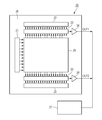
- FIG. 3 is a schematic cross-sectional view showing an example of the photoelectric conversion element according to this embodiment.
- a photoelectric conversion layer 1 for converting light into electric charge is disposed between an anode electrode 4 and a cathode electrode 5 which are a pair of electrodes.
- a protective layer 7, a wavelength selection unit 8, and a microlens 9 are disposed on the anode electrode.
- a readout circuit 6 is connected to the cathode electrode.
- an electrode close to the substrate may be called a lower electrode, and an electrode far from the substrate may be called an upper electrode.
- the lower electrode may be an anode electrode or a cathode electrode.
- the lower electrode may be an electrode having a high reflectance.
- the electrode may be made of a highly reflective material, or may have a reflective layer in addition to the electrode layer.
- the photoelectric conversion element according to the present invention may have a substrate.
- a substrate for example, a silicon substrate, a glass substrate, a flexible substrate, or the like can be used.
- the cathode electrode included in the photoelectric conversion element according to the present invention is an electrode that collects holes out of charges generated in the photoelectric conversion layer.
- the anode electrode is an electrode that collects electrons among the charges generated in the photoelectric conversion layer.
- the material constituting the cathode electrode and the anode electrode is not limited as long as it has high conductivity and transparency. The materials constituting the cathode electrode and the anode electrode may be the same or different.
- the electrode material include metals, metal oxides, metal nitrides, metal borides, organic conductive compounds, and mixtures thereof, and more specifically, doped with antimony or fluorine.
- Conductive metal oxides such as tin oxide (ATO, FTO), tin oxide, zinc oxide, indium oxide, indium tin oxide (ITO), indium zinc oxide (IZO), gold, silver, chromium, nickel, titanium, tungsten, Metals such as aluminum and conductive compounds such as oxides and nitrides of these metals (for example, titanium nitride (TiN)), and mixtures or laminates of these metals and conductive metal oxides, iodinated Examples include inorganic conductive materials such as copper and copper sulfide, organic conductive materials such as polyaniline, polythiophene, and polypyrrole, and laminates of these with ITO or titanium nitride. It is. Particularly preferable materials for the electrode include titanium nitride, molyb
- the hole or electron collection electrode of the photoelectric conversion element is an electrode that collects either the charge generated in the photoelectric conversion layer.
- the collecting electrode in the lower part may be a pixel electrode in the configuration of the imaging device. Whether the pixel electrode is a cathode or an anode depends on the element configuration and the underlying circuit configuration. For example, the order of substrate / anode electrode / photoelectric conversion layer / cathode electrode may be provided on the substrate, or the order of substrate / cathode electrode / photoelectric conversion layer / anode electrode may be used.
- the method for forming the electrode can be appropriately selected in consideration of suitability with the electrode material. Specifically, it can be formed by a wet method such as a printing method or a coating method, a physical method such as a vacuum deposition method, a sputtering method, or an ion plating method, or a chemical method such as CVD or plasma CVD method.
- the electrode When the electrode is ITO, it can be formed by a method such as an electron beam method, a sputtering method, a resistance heating vapor deposition method, a chemical reaction method (sol-gel method or the like), or a dispersion of indium tin oxide. Furthermore, the formed ITO can be subjected to UV-ozone treatment, plasma treatment, and the like. When the electrode is TiN, various methods such as a reactive sputtering method can be used, and annealing treatment, UV-ozone treatment, plasma treatment, and the like can be further performed.
- the photoelectric conversion layer may have an organic compound in addition to the general formulas [1] to [5].
- organic compound for example, triarylamine compounds, pyran compounds, quinacridone compounds, benzidine compounds, pyrazoline compounds, styrylamine compounds, hydrazone compounds, triphenylmethane compounds, carbazole compounds, polysilane compounds, thiophene compounds, phthalocyanine compounds, cyanine compounds, merocyanine compounds, oxonol Compound, polyamine compound, indole compound, pyrrole compound, pyrazole compound, polyarylene compound, condensed aromatic carbocyclic compound (naphthalene derivative, anthracene derivative, phenanthrene derivative, tetracene derivative, pyrene derivative, perylene derivative, fluoranthene derivative), nitrogen-containing hetero
- a metal complex having a ring compound as a ligand can be used.
- the fluoranthene derivative is a compound having a fluoranthene skeleton in the chemical structural formula. It also includes compounds in which a condensed ring is added to the fluoranthene skeleton. That is, it means a compound in which a fluoranthene skeleton is found from the chemical structural formula.
- naphthalene derivatives anthracene derivatives, phenanthrene derivatives, tetracene derivatives, pyrene derivatives, and perylene derivatives.
- the photoelectric conversion layer may have fullerene or a fullerene derivative as the second organic compound.
- Fullerene or a fullerene derivative may function as an n-type organic semiconductor.
- Fullerene or fullerene derivative molecules are connected in the photoelectric conversion layer, whereby an electron transport path is formed. Therefore, the electron transport property is improved, and the high-speed response of the photoelectric conversion element is improved.
- the weight ratio of fullerene or fullerene derivative is preferably 40% by weight or more and 85% by weight or less when the total of the first organic compound and the second organic compound is 100% by weight.
- fullerene or fullerene derivatives include fullerene C60, fullerene C70, fullerene C76, fullerene C78, fullerene C80, fullerene C82, fullerene C84, fullerene C90, fullerene C96, fullerene C240, fullerene 540, mixed fullerene, and fullerene nanotubes. It is done.
- the fullerene derivative may have a substituent.
- this substituent include an alkyl group, an aryl group, and a heterocyclic group.
- the fullerene derivative is preferably fullerene C60.
- the photoelectric conversion layer preferably does not emit light.
- the term “non-emission” means that the emission quantum efficiency is 1% or less, preferably 0.5% or less, more preferably 0.1% or less in the visible light region (wavelength 400 nm to 730 nm). If the light-emitting quantum efficiency of the photoelectric conversion layer is within 1%, it is preferable as an image sensor because it has little influence on sensing performance or image performance even when applied to a sensor or an image sensor.
- the photoelectric conversion element according to the present invention may further include a hole blocking layer between the anode electrode and the photoelectric conversion layer.
- the hole blocking layer is a layer that suppresses the flow of holes from the anode electrode to the photoelectric conversion layer, and preferably has a high ionization potential.
- the photoelectric conversion element according to the present invention may further have an electron blocking layer between the cathode electrode and the photoelectric conversion layer.
- the electron blocking layer is a layer that suppresses electrons from flowing from the cathode electrode to the photoelectric conversion layer, and preferably has a low electron affinity or LUMO (minimum unoccupied molecular orbital).
- silicon oxide, silicon nitride, silicon nitride oxide, aluminum oxide, and the like can be given. Silicon oxide, silicon nitride, and silicon nitride oxide can be formed by a sputtering method or a CVD method, and aluminum oxide can be formed by an ALD method (atomic layer deposition method).
- the sealing performance of the sealing layer may be such that the water permeability is 10 ⁇ 5 g / m 2 ⁇ day or less.
- the layer thickness of the sealing layer is not particularly limited, but is preferably 0.5 ⁇ m or more from the viewpoint of sealing performance. On the other hand, if the sealing performance can be maintained, the thinner one is preferable, and the thickness is particularly preferably 1 ⁇ m or less.
- the sealing layer is thin is that, when used as an image sensor, the effect of reducing color mixing is the shorter the distance from the photoelectric conversion layer to the color filter.
- the annealing temperature is not limited, the annealing temperature may be 150 ° C. or higher and 190 ° C. or lower. The annealing temperature is appropriately determined in view of the annealing time.
- Exemplified compounds 1-1 to 1-23 are a group of compounds mainly having a 5-membered heterocyclic group containing a sulfur atom. This is because the absorption intensity in the long wavelength region in the visible region is increased by the 5-membered heterocyclic group containing a sulfur atom. As a result, it can contribute to the panchromic property of the photoelectric conversion layer.
- the exemplary compounds 1-1 to 1-23 are preferable because they exhibit long-life light emission.
- Exemplified compounds 2-1 to 2-56 are a group of compounds having a fluoranthene skeleton as a center. Since the fluoranthene skeleton exhibits long-life luminescence and has a low reduction potential, it is preferable as the first organic compound.
- Exemplified compounds 3-1 to 3-14 are a metal complex compound group. These metal complex compounds are compounds that exhibit phosphorescence emission, and are preferable as the first organic compound because the exciton lifetime is longer than that of a fluorescent organic compound.
- the imaging device includes a plurality of pixels, and each pixel includes a photoelectric conversion device according to the present invention and a readout transistor connected to the photoelectric conversion device.
- the plurality of pixels may be arranged in a matrix including a plurality of rows and a plurality of columns.
- Each pixel may be connected to a signal processing circuit.
- the signal processing circuit can obtain an image by receiving a signal from each pixel.
- the readout transistor is a transistor that transfers a signal based on the electric charge generated in the photoelectric conversion element.
- the signal processing circuit may be a CMOS sensor or a CCD sensor.
- the image sensor may have an optical filter, for example, a color filter.
- a color filter When the photoelectric conversion element corresponds to light of a specific wavelength, it is preferable to have a color filter corresponding to the photoelectric conversion element.
- the color filter may be provided with one color filter for one light receiving pixel or one color filter for a plurality of light receiving pixels.
- optical filter examples include a color filter, a low-pass filter that transmits wavelengths of infrared rays or more, and a UV cut filter that transmits wavelengths of ultraviolet rays or less.
- the image sensor may have an optical member such as a microlens.
- the microlens is a lens that collects light from the outside onto the photoelectric conversion layer.
- one microlens may be provided for one light receiving pixel, or one microlens corresponding to a plurality of light receiving pixels may be provided. When a plurality of light receiving pixels are provided, it is preferable that one microlens is provided for each of the plurality of light receiving pixels.
- the imaging device can be used in an imaging device.
- the imaging apparatus includes an imaging optical system having a plurality of lenses, and an imaging element that receives light that has passed through the imaging optical system.
- the imaging device may include an imaging element and a housing that houses the imaging element, and the housing may include a joint that can be joined to the imaging optical system. More specifically, the imaging device is a digital camera or a digital still camera.
- the imaging apparatus may further include a receiving unit that performs an external signal.
- the signal received by the receiving unit is a signal that controls at least one of the imaging range of the imaging device, the start of imaging, and the end of imaging.
- the imaging device may further include a transmission unit that transmits the acquired image to the outside. Examples of the acquired image include a captured image and an image transmitted from another device.
- FIG. 4 is a circuit diagram showing an example of a pixel including the photoelectric conversion device according to the present invention.
- the photoelectric conversion device 10 is connected to the common wiring 19 at nodeA.
- the common wiring may be connected to the ground.
- the pixel 18 may include a photoelectric conversion element 10 and a read circuit for reading a signal generated in the photoelectric conversion unit.
- the readout circuit includes, for example, a transfer transistor 11 electrically connected to the photoelectric conversion element, an amplification transistor 13 having a gate electrode electrically connected to the photoelectric conversion element 10, a selection transistor 14 for selecting a pixel from which information is read, a photoelectric transistor A reset transistor 12 that supplies a reset voltage to the conversion element may be included.
- the transfer transistor 11 may be controlled to transfer by pTX.
- the reset transistor may be controlled in voltage supply by pRES.
- the selection transistor is selected or not selected by pSEL.
- the transfer transistor 11, the reset transistor 12, and the amplifying transistor 13 are connected by nodeB. Depending on the configuration, the transfer transistor may not be provided.
- the reset transistor is a transistor that supplies a voltage for resetting the potential of nodeB.
- the voltage supply can be controlled by applying pRES to the gate of the reset transistor. Depending on the configuration, the reset transistor may not be provided.
- the amplification transistor is a transistor that passes a current corresponding to the potential of nodeB.
- the amplification transistor is connected to a selection transistor 14 that selects a pixel that outputs a signal.
- the selection transistor is connected to the current source 16 and the column output unit 15, and the column output unit 15 may be connected to the signal processing unit.
- the selection transistor 14 is connected to the vertical output signal line 17.
- the vertical output signal line 17 is connected to the current source 16 and the column output unit 15.
- FIG. 5 is a schematic diagram showing the image sensor according to the present invention and its peripheral circuits.
- the imaging element 20 has an imaging region 25 in which a plurality of pixels are two-dimensionally arranged, and a peripheral region 26.
- the area other than the imaging area is a peripheral area.
- the peripheral area has a vertical scanning circuit 21, a readout circuit 22, a horizontal scanning circuit 23, and an output amplifier 24, and the output amplifier is connected to a signal processing unit 27.
- the signal processing unit is a signal processing unit that performs signal processing based on information read by the reading circuit, and examples thereof include a CCD circuit and a CMOS circuit.
- the readout circuit 22 includes, for example, a column amplifier, a CDS circuit, an addition circuit, and the like, and amplifies and adds signals read out from the pixels in the row selected by the vertical scanning circuit 21 through the vertical signal line.
- the column amplifier, the CDS circuit, the addition circuit, and the like are arranged for each pixel column or a plurality of pixel columns, for example.
- the horizontal scanning circuit 23 generates a signal for sequentially reading the signals of the reading circuit 22.
- the output amplifier 24 amplifies and outputs the signal of the column selected by the horizontal scanning circuit 23.
- the above configuration is only one configuration example of the photoelectric conversion device, and the present embodiment is not limited to this.
- the readout circuit 22, the horizontal scanning circuit 23, and the output amplifier 24 are arranged one above the other with the imaging region 25 interposed therebetween so as to constitute two systems of output paths. However, three or more output paths may be provided. Signals output from the output amplifiers are combined as image signals by the signal processing unit.
- Excitation light source Picosecond light pulser manufactured by Hamamatsu Photonics (emission wavelength: 442 nm)
- Spectrometer Hamamatsu Photonics Imaging Spectrograph C5094 Detector: Streak scope C4334 manufactured by Hamamatsu Photonics
- Example preparation Each compound was dissolved in chloroform, the concentration was adjusted so that the absorbance at a wavelength of 442 nm was about 0.05 to 0.2, and about 3 mL of the solution was put in a cell having an optical path length of 1 cm.
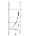
- FIG. 6 is a diagram illustrating an example of an attenuation curve of light emission intensity.
- the decay curve was analyzed with one-component decay to obtain the light emission lifetime.
- the light emission lifetime was defined as the time until the initial intensity reached 1 / e.
- Table 1 shows the light emission lifetimes of the exemplified compounds of the first organic compound.
- Example 1 a photoelectric conversion element having a first organic compound having a light emission lifetime in a chloroform solution of 1.1 nanoseconds or more and a second organic compound was produced. Element characteristics were evaluated using the produced elements.
- a photoelectric conversion element was formed on a Si substrate.
- a cathode electrode, an electron block layer, a photoelectric conversion layer, a hole block layer, and an anode electrode are sequentially formed.
- the photoelectric conversion element was manufactured by the following steps.
- a Si substrate was prepared in which a wiring layer and an insulating layer were laminated, and contact holes were formed in the insulating layer from the wiring layer at locations corresponding to the respective pixels so as to be conductive. This contact hole is connected to the pad portion at the end of the substrate by wiring.
- An IZO electrode was formed by a sputtering method so as to overlap this contact hole portion. Patterning was performed to form an IZO electrode (cathode electrode) of 3 mm 2 . At this time, the thickness of the IZO electrode was set to 100 nm.
- An organic compound layer was formed on the IZO electrode by a vacuum deposition method.
- the layer configuration and layer thickness are as shown in Table 3 below.
- IZO was formed by sputtering as an anode electrode.
- the thickness of the anode electrode was 30 nm.
- Table 3 shows the layer structure of the photoelectric conversion element.
- Table 3 shows the cathode as the lower electrode on the lower side of the table.
- the following compound (d-1) was used for the electron blocking layer.
- the first organic compound of the photoelectric conversion layer is exemplified compounds 1-1 to 3-14, and the hole blocking layer is fullerene C60 (d-2) and C70 (d-3) and the following organic compound (d- Any of 4) was used.
- hollow sealing was performed using a glass cap and an ultraviolet curable resin.
- the element thus obtained was annealed for about 1 hour on a hot plate at 170 ° C. with the sealing surface facing upward.
- the characteristics of the photoelectric conversion element were measured and evaluated for the obtained element. When the current when 5 V was applied to the device was confirmed, it was confirmed that the photoelectric conversion device was functioning because the current value in the light place was 100 times or more the current value in the dark place. .
- the external quantum efficiency of the obtained device is as follows. When a voltage of 5 V is applied between the cathode electrode and the anode electrode, the device that produced monochromatic light with 550 nm (green light) and intensity of 50 ⁇ W / cm 2 is irradiated. It was calculated by measuring the flowing photocurrent density.
- the photocurrent density was obtained by subtracting the dark current density during light shielding from the current density during light irradiation.
- the monochromatic light used for the measurement was monochromatic with white light emitted from a xenon lamp (device name: XB-50101AA-A, manufactured by USHIO INC.) Using a monochromator (device name: MC-10N, manufactured by Retsu Applied Optics). Voltage application to the element and current measurement were performed using a source meter (device name R6243, manufactured by Advantest). In addition, light was irradiated perpendicularly to the electrode from the upper electrode side of the produced photoelectric conversion element.
- the absorption rate was measured with a SolidSpec-3700UV-VIS-NIR-Spectrophotometer manufactured by Shimadzu Corporation. At the time of measurement, a sample in which a film having the same structure as the photoelectric conversion layer was formed on a quartz substrate was prepared, and the absorption rate of this film was obtained.
- Examples 2 to 22, Comparative Examples 1 to 9 A photoelectric conversion element was produced in the same manner as in Example 1 except that the combination of organic compounds contained in the photoelectric conversion layer was changed to the combination shown in Table 6, and the photoelectric conversion efficiency was evaluated. In Examples 17 to 22, a phosphorescent material was used as the first organic compound layer.
- Organic compounds e-1 to e-3 used in Comparative Examples 1 to 9 are organic compounds represented by the following structural formulas.
- Table 5 shows the luminescence lifetime of organic compounds e-1 to e-3 in a chloroform solution and the reduction potential in orthodichlorobenzene.
- Table 6 shows the results of Examples 1 to 22 and Comparative Examples 1 to 9.
- the evaluation criteria for photoelectric conversion efficiency were as follows. A: 75% or more B: 65% or more and less than 75% C: less than 65%
- B determination or more was judged good and C was judged as defective.
- the photoelectric conversion efficiency was equal to or higher than evaluation B for any combination of photoelectric conversion elements. Furthermore, when the emission lifetime of the first organic compound is 1.1 nanoseconds or more and ⁇ Ered ⁇ 0.32, higher photoelectric conversion efficiency is obtained.
- An organic compound having a ⁇ Ered greater than 0.65 is an organic compound having a low oxidation potential. As a result, the dark current of the photoelectric conversion element tends to increase.
Landscapes
- Chemical & Material Sciences (AREA)
- Organic Chemistry (AREA)
- Engineering & Computer Science (AREA)
- Materials Engineering (AREA)
- Physics & Mathematics (AREA)
- Spectroscopy & Molecular Physics (AREA)
- Nanotechnology (AREA)
- Electromagnetism (AREA)
- Inorganic Chemistry (AREA)
- Crystallography & Structural Chemistry (AREA)
- Light Receiving Elements (AREA)
- Solid State Image Pick-Up Elements (AREA)
- Thiazole And Isothizaole Compounds (AREA)
- Organic Low-Molecular-Weight Compounds And Preparation Thereof (AREA)
- Electroluminescent Light Sources (AREA)
- Heterocyclic Compounds Containing Sulfur Atoms (AREA)
Priority Applications (1)
| Application Number | Priority Date | Filing Date | Title |
|---|---|---|---|
| US16/405,874 US20190267545A1 (en) | 2016-11-11 | 2019-05-07 | Photoelectric conversion element, and imaging element and imaging apparatus including the same |
Applications Claiming Priority (2)
| Application Number | Priority Date | Filing Date | Title |
|---|---|---|---|
| JP2016220716A JP2018078242A (ja) | 2016-11-11 | 2016-11-11 | 光電変換素子、それを有する撮像素子及び撮像装置 |
| JP2016-220716 | 2016-11-11 |
Related Child Applications (1)
| Application Number | Title | Priority Date | Filing Date |
|---|---|---|---|
| US16/405,874 Continuation US20190267545A1 (en) | 2016-11-11 | 2019-05-07 | Photoelectric conversion element, and imaging element and imaging apparatus including the same |
Publications (1)
| Publication Number | Publication Date |
|---|---|
| WO2018088313A1 true WO2018088313A1 (ja) | 2018-05-17 |
Family
ID=62110668
Family Applications (1)
| Application Number | Title | Priority Date | Filing Date |
|---|---|---|---|
| PCT/JP2017/039669 Ceased WO2018088313A1 (ja) | 2016-11-11 | 2017-11-02 | 光電変換素子、それを有する撮像素子及び撮像装置 |
Country Status (3)
| Country | Link |
|---|---|
| US (1) | US20190267545A1 (https=) |
| JP (1) | JP2018078242A (https=) |
| WO (1) | WO2018088313A1 (https=) |
Cited By (2)
| Publication number | Priority date | Publication date | Assignee | Title |
|---|---|---|---|---|
| CN113498411A (zh) * | 2019-01-16 | 2021-10-12 | 香港科技大学 | 具有广泛颜色可调性以及聚集诱导发光特征的荧光化合物 |
| KR20250131481A (ko) * | 2024-02-27 | 2025-09-03 | 경상국립대학교산학협력단 | 로다닌기가 도입된 헤테로환 화합물, 이를 포함하는 유기 반도체 및 광전 변환 소자 |
Families Citing this family (4)
| Publication number | Priority date | Publication date | Assignee | Title |
|---|---|---|---|---|
| JP7433741B2 (ja) * | 2016-05-31 | 2024-02-20 | キヤノン株式会社 | 光電変換素子、二次元センサ、画像センサおよび撮像装置 |
| JP7325731B2 (ja) | 2018-08-23 | 2023-08-15 | 国立大学法人九州大学 | 有機エレクトロルミネッセンス素子 |
| GB2579416A (en) | 2018-11-30 | 2020-06-24 | Sumitomo Chemical Co | Photoactive compound |
| CN112174839A (zh) * | 2020-11-05 | 2021-01-05 | 四川大学华西医院 | 一种脂滴特异性标记的荧光探针及其合成方法和应用 |
Citations (8)
| Publication number | Priority date | Publication date | Assignee | Title |
|---|---|---|---|---|
| JP2007059517A (ja) * | 2005-08-23 | 2007-03-08 | Fujifilm Corp | 光電変換膜、光電変換素子、及び撮像素子、並びに、これらに電場を印加する方法 |
| JP2009132674A (ja) * | 2007-10-31 | 2009-06-18 | Idemitsu Kosan Co Ltd | アセナフトフルオランテン化合物からなる光電変換素子用材料及びそれを用いた光電変換素子 |
| JP2009290091A (ja) * | 2008-05-30 | 2009-12-10 | Idemitsu Kosan Co Ltd | 有機薄膜太陽電池用材料及びそれを用いた有機薄膜太陽電池 |
| JP2010093100A (ja) * | 2008-10-09 | 2010-04-22 | Konica Minolta Holdings Inc | 有機光電変換素子、太陽電池及び光センサアレイ |
| WO2011077198A1 (es) * | 2009-12-22 | 2011-06-30 | Ecopetrol S.A. | Sistema para deshidratacion y desalado de hidrocarburos |
| WO2012032990A1 (ja) * | 2010-09-08 | 2012-03-15 | 富士フイルム株式会社 | 光電変換材料、該材料を含む膜、光電変換素子、光電変換素子の製造方法、光電変換素子の使用方法、光センサ、撮像素子 |
| WO2012157110A1 (ja) * | 2011-05-19 | 2012-11-22 | Dic株式会社 | フタロシアニンナノロッド、及び光電変換素子 |
| FR3011548A1 (fr) * | 2013-10-07 | 2015-04-10 | Arkema France | Compose organique photoactif |
Family Cites Families (2)
| Publication number | Priority date | Publication date | Assignee | Title |
|---|---|---|---|---|
| JP5520560B2 (ja) * | 2009-09-29 | 2014-06-11 | 富士フイルム株式会社 | 光電変換素子、光電変換素子材料、光センサ、及び撮像素子 |
| WO2012170456A2 (en) * | 2011-06-06 | 2012-12-13 | University Of Florida Research Foundation, Inc. | Infrared imaging device integrating an ir up-conversion device with a cmos image sensor |
-
2016
- 2016-11-11 JP JP2016220716A patent/JP2018078242A/ja active Pending
-
2017
- 2017-11-02 WO PCT/JP2017/039669 patent/WO2018088313A1/ja not_active Ceased
-
2019
- 2019-05-07 US US16/405,874 patent/US20190267545A1/en not_active Abandoned
Patent Citations (8)
| Publication number | Priority date | Publication date | Assignee | Title |
|---|---|---|---|---|
| JP2007059517A (ja) * | 2005-08-23 | 2007-03-08 | Fujifilm Corp | 光電変換膜、光電変換素子、及び撮像素子、並びに、これらに電場を印加する方法 |
| JP2009132674A (ja) * | 2007-10-31 | 2009-06-18 | Idemitsu Kosan Co Ltd | アセナフトフルオランテン化合物からなる光電変換素子用材料及びそれを用いた光電変換素子 |
| JP2009290091A (ja) * | 2008-05-30 | 2009-12-10 | Idemitsu Kosan Co Ltd | 有機薄膜太陽電池用材料及びそれを用いた有機薄膜太陽電池 |
| JP2010093100A (ja) * | 2008-10-09 | 2010-04-22 | Konica Minolta Holdings Inc | 有機光電変換素子、太陽電池及び光センサアレイ |
| WO2011077198A1 (es) * | 2009-12-22 | 2011-06-30 | Ecopetrol S.A. | Sistema para deshidratacion y desalado de hidrocarburos |
| WO2012032990A1 (ja) * | 2010-09-08 | 2012-03-15 | 富士フイルム株式会社 | 光電変換材料、該材料を含む膜、光電変換素子、光電変換素子の製造方法、光電変換素子の使用方法、光センサ、撮像素子 |
| WO2012157110A1 (ja) * | 2011-05-19 | 2012-11-22 | Dic株式会社 | フタロシアニンナノロッド、及び光電変換素子 |
| FR3011548A1 (fr) * | 2013-10-07 | 2015-04-10 | Arkema France | Compose organique photoactif |
Cited By (4)
| Publication number | Priority date | Publication date | Assignee | Title |
|---|---|---|---|---|
| CN113498411A (zh) * | 2019-01-16 | 2021-10-12 | 香港科技大学 | 具有广泛颜色可调性以及聚集诱导发光特征的荧光化合物 |
| KR20250131481A (ko) * | 2024-02-27 | 2025-09-03 | 경상국립대학교산학협력단 | 로다닌기가 도입된 헤테로환 화합물, 이를 포함하는 유기 반도체 및 광전 변환 소자 |
| WO2025183456A1 (ko) * | 2024-02-27 | 2025-09-04 | 경상국립대학교산학협력단 | 로다닌기가 도입된 헤테로환 화합물, 이를 포함하는 유기 반도체 및 광전 변환 소자 |
| KR102868214B1 (ko) | 2024-02-27 | 2025-10-14 | 경상국립대학교산학협력단 | 로다닌기가 도입된 헤테로환 화합물, 이를 포함하는 유기 반도체 및 광전 변환 소자 |
Also Published As
| Publication number | Publication date |
|---|---|
| US20190267545A1 (en) | 2019-08-29 |
| JP2018078242A (ja) | 2018-05-17 |
Similar Documents
| Publication | Publication Date | Title |
|---|---|---|
| JP7102114B2 (ja) | 光電変換素子、撮像素子および撮像装置 | |
| WO2018088313A1 (ja) | 光電変換素子、それを有する撮像素子及び撮像装置 | |
| EP3961737B1 (en) | Composition for photoelectric device, and image sensor and electronic device including the same | |
| CN110301052B (zh) | 光电转换元件、和使用其的光学区域传感器、图像拾取元件和图像拾取设备 | |
| JP6645700B2 (ja) | 有機光電変換素子、二次元センサ、画像センサ及び撮像装置 | |
| JP6700825B2 (ja) | 有機光電変換素子、光エリアセンサ、撮像素子及び撮像装置 | |
| KR20210091064A (ko) | 화합물 및 이를 포함하는 광전 소자, 이미지 센서 및 전자 장치 | |
| JP2015233117A (ja) | 光電変換膜、固体撮像素子、および電子機器 | |
| JP7013163B2 (ja) | 有機化合物及び光電変換素子 | |
| JP6932564B2 (ja) | 有機光電変換素子、撮像素子及び撮像装置 | |
| KR20170104999A (ko) | 광전 변환 소자 및 이것을 사용한 이미지 센서 | |
| JP7051332B2 (ja) | 有機化合物及び光電変換素子 | |
| WO2018147202A1 (ja) | 光電変換素子、及びこれを用いた光エリアセンサ、撮像素子、撮像装置 | |
| JP7791700B2 (ja) | インドロカルバゾール環を有する化合物、受光素子用材料、有機薄膜、受光素子、及び撮像素子 | |
| JP7039285B2 (ja) | 光電変換素子、及びこれを用いた光エリアセンサ、撮像素子、撮像装置 | |
| JP2019055919A (ja) | 有機化合物及び光電変換素子 | |
| WO2018088325A1 (ja) | 光電変換素子、撮像素子および撮像装置 | |
| JP7086573B2 (ja) | 光電変換素子、及びこれを用いた光エリアセンサ、撮像素子、撮像装置 | |
| JP2018002690A (ja) | 有機化合物、有機光電変換素子、撮像素子および撮像装置 | |
| JP7516590B2 (ja) | 光電変換膜および光電変換素子 | |
| JP7016662B2 (ja) | 有機化合物、それを用いた光電変換素子および撮像装置 | |
| JP2018078240A (ja) | 光電変換素子、それを有する撮像素子及び撮像装置 | |
| JP2017174921A (ja) | 有機光電変換素子、二次元センサ、画像センサ及び撮像装置 | |
| JP7850964B2 (ja) | 有機受光素子及び受光装置 | |
| CN112645944B (zh) | 化合物以及包括其的光电器件、图像传感器和电子设备 |
Legal Events
| Date | Code | Title | Description |
|---|---|---|---|
| 121 | Ep: the epo has been informed by wipo that ep was designated in this application |
Ref document number: 17868527 Country of ref document: EP Kind code of ref document: A1 |
|
| NENP | Non-entry into the national phase |
Ref country code: DE |
|
| 122 | Ep: pct application non-entry in european phase |
Ref document number: 17868527 Country of ref document: EP Kind code of ref document: A1 |