WO2018088325A1 - 光電変換素子、撮像素子および撮像装置 - Google Patents
光電変換素子、撮像素子および撮像装置 Download PDFInfo
- Publication number
- WO2018088325A1 WO2018088325A1 PCT/JP2017/039722 JP2017039722W WO2018088325A1 WO 2018088325 A1 WO2018088325 A1 WO 2018088325A1 JP 2017039722 W JP2017039722 W JP 2017039722W WO 2018088325 A1 WO2018088325 A1 WO 2018088325A1
- Authority
- WO
- WIPO (PCT)
- Prior art keywords
- group
- substituted
- photoelectric conversion
- unsubstituted
- organic compound
- Prior art date
Links
- 238000006243 chemical reaction Methods 0.000 title claims abstract description 145
- 238000003384 imaging method Methods 0.000 title claims description 37
- 150000002894 organic compounds Chemical class 0.000 claims abstract description 101
- 125000001424 substituent group Chemical group 0.000 claims abstract description 25
- 230000003647 oxidation Effects 0.000 claims abstract description 24
- 238000007254 oxidation reaction Methods 0.000 claims abstract description 24
- 125000004435 hydrogen atom Chemical group [H]* 0.000 claims abstract description 13
- 229910052799 carbon Inorganic materials 0.000 claims abstract description 10
- 229910052757 nitrogen Inorganic materials 0.000 claims abstract description 9
- 125000004430 oxygen atom Chemical group O* 0.000 claims abstract description 9
- 229910052717 sulfur Inorganic materials 0.000 claims abstract description 7
- 125000004433 nitrogen atom Chemical group N* 0.000 claims abstract description 6
- 125000004434 sulfur atom Chemical group 0.000 claims abstract description 5
- 125000003118 aryl group Chemical group 0.000 claims description 34
- 125000000623 heterocyclic group Chemical group 0.000 claims description 33
- XMWRBQBLMFGWIX-UHFFFAOYSA-N C60 fullerene Chemical class C12=C3C(C4=C56)=C7C8=C5C5=C9C%10=C6C6=C4C1=C1C4=C6C6=C%10C%10=C9C9=C%11C5=C8C5=C8C7=C3C3=C7C2=C1C1=C2C4=C6C4=C%10C6=C9C9=C%11C5=C5C8=C3C3=C7C1=C1C2=C4C6=C2C9=C5C3=C12 XMWRBQBLMFGWIX-UHFFFAOYSA-N 0.000 claims description 27
- 230000004913 activation Effects 0.000 claims description 24
- 125000005843 halogen group Chemical group 0.000 claims description 23
- 238000010521 absorption reaction Methods 0.000 claims description 22
- 125000000217 alkyl group Chemical group 0.000 claims description 22
- 125000003545 alkoxy group Chemical group 0.000 claims description 18
- 229910052751 metal Inorganic materials 0.000 claims description 18
- 239000002184 metal Substances 0.000 claims description 18
- 125000003277 amino group Chemical group 0.000 claims description 17
- 125000004093 cyano group Chemical group *C#N 0.000 claims description 17
- 239000003446 ligand Substances 0.000 claims description 15
- 125000000391 vinyl group Chemical group [H]C([*])=C([H])[H] 0.000 claims description 13
- 238000007789 sealing Methods 0.000 claims description 12
- HEDRZPFGACZZDS-UHFFFAOYSA-N Chloroform Chemical compound ClC(Cl)Cl HEDRZPFGACZZDS-UHFFFAOYSA-N 0.000 claims description 10
- 238000012545 processing Methods 0.000 claims description 10
- 125000004429 atom Chemical group 0.000 claims description 9
- 150000001721 carbon Chemical group 0.000 claims description 9
- 230000003287 optical effect Effects 0.000 claims description 8
- BASFCYQUMIYNBI-UHFFFAOYSA-N platinum Chemical compound [Pt] BASFCYQUMIYNBI-UHFFFAOYSA-N 0.000 claims description 6
- RTAQQCXQSZGOHL-UHFFFAOYSA-N Titanium Chemical compound [Ti] RTAQQCXQSZGOHL-UHFFFAOYSA-N 0.000 claims description 3
- 125000001072 heteroaryl group Chemical group 0.000 claims description 3
- 229910052697 platinum Inorganic materials 0.000 claims description 3
- 239000010936 titanium Substances 0.000 claims description 3
- 229910052719 titanium Inorganic materials 0.000 claims description 3
- GYHNNYVSQQEPJS-UHFFFAOYSA-N Gallium Chemical compound [Ga] GYHNNYVSQQEPJS-UHFFFAOYSA-N 0.000 claims description 2
- 230000005540 biological transmission Effects 0.000 claims description 2
- 229910017052 cobalt Inorganic materials 0.000 claims description 2
- 239000010941 cobalt Substances 0.000 claims description 2
- GUTLYIVDDKVIGB-UHFFFAOYSA-N cobalt atom Chemical compound [Co] GUTLYIVDDKVIGB-UHFFFAOYSA-N 0.000 claims description 2
- 229910052733 gallium Inorganic materials 0.000 claims description 2
- 229910052741 iridium Inorganic materials 0.000 claims description 2
- GKOZUEZYRPOHIO-UHFFFAOYSA-N iridium atom Chemical compound [Ir] GKOZUEZYRPOHIO-UHFFFAOYSA-N 0.000 claims description 2
- 229910052720 vanadium Inorganic materials 0.000 claims description 2
- LEONUFNNVUYDNQ-UHFFFAOYSA-N vanadium atom Chemical compound [V] LEONUFNNVUYDNQ-UHFFFAOYSA-N 0.000 claims 1
- 150000001875 compounds Chemical class 0.000 abstract description 35
- 125000004432 carbon atom Chemical group C* 0.000 abstract description 9
- 230000009467 reduction Effects 0.000 abstract description 9
- 150000002219 fluoranthenes Chemical class 0.000 abstract description 2
- 150000004696 coordination complex Chemical class 0.000 abstract 1
- 239000010410 layer Substances 0.000 description 94
- -1 triarylamine compound Chemical class 0.000 description 64
- 239000000463 material Substances 0.000 description 19
- 238000000034 method Methods 0.000 description 15
- 229910003472 fullerene Inorganic materials 0.000 description 14
- 239000004065 semiconductor Substances 0.000 description 14
- 239000000758 substrate Substances 0.000 description 14
- 125000005842 heteroatom Chemical group 0.000 description 9
- 238000010586 diagram Methods 0.000 description 8
- 230000000903 blocking effect Effects 0.000 description 7
- 230000000052 comparative effect Effects 0.000 description 7
- 125000003914 fluoranthenyl group Chemical group C1(=CC=C2C=CC=C3C4=CC=CC=C4C1=C23)* 0.000 description 7
- IJGRMHOSHXDMSA-UHFFFAOYSA-N Atomic nitrogen Chemical compound N#N IJGRMHOSHXDMSA-UHFFFAOYSA-N 0.000 description 6
- 229910052581 Si3N4 Inorganic materials 0.000 description 6
- 238000000137 annealing Methods 0.000 description 6
- 238000002484 cyclic voltammetry Methods 0.000 description 6
- 238000011156 evaluation Methods 0.000 description 6
- 229910052731 fluorine Inorganic materials 0.000 description 6
- HQVNEWCFYHHQES-UHFFFAOYSA-N silicon nitride Chemical compound N12[Si]34N5[Si]62N3[Si]51N64 HQVNEWCFYHHQES-UHFFFAOYSA-N 0.000 description 6
- 238000012546 transfer Methods 0.000 description 6
- 125000006267 biphenyl group Chemical group 0.000 description 5
- 125000000484 butyl group Chemical group [H]C([*])([H])C([H])([H])C([H])([H])C([H])([H])[H] 0.000 description 5
- 230000005284 excitation Effects 0.000 description 5
- 125000001153 fluoro group Chemical group F* 0.000 description 5
- 238000005259 measurement Methods 0.000 description 5
- 125000001997 phenyl group Chemical group [H]C1=C([H])C([H])=C(*)C([H])=C1[H] 0.000 description 5
- 238000000926 separation method Methods 0.000 description 5
- 238000004544 sputter deposition Methods 0.000 description 5
- NRTOMJZYCJJWKI-UHFFFAOYSA-N Titanium nitride Chemical compound [Ti]#N NRTOMJZYCJJWKI-UHFFFAOYSA-N 0.000 description 4
- 150000002739 metals Chemical class 0.000 description 4
- 230000002093 peripheral effect Effects 0.000 description 4
- 125000002080 perylenyl group Chemical class C1(=CC=C2C=CC=C3C4=CC=CC5=CC=CC(C1=C23)=C45)* 0.000 description 4
- 125000004076 pyridyl group Chemical group 0.000 description 4
- 125000000168 pyrrolyl group Chemical group 0.000 description 4
- YJTKZCDBKVTVBY-UHFFFAOYSA-N 1,3-Diphenylbenzene Chemical group C1=CC=CC=C1C1=CC=CC(C=2C=CC=CC=2)=C1 YJTKZCDBKVTVBY-UHFFFAOYSA-N 0.000 description 3
- ZCYVEMRRCGMTRW-UHFFFAOYSA-N 7553-56-2 Chemical group [I] ZCYVEMRRCGMTRW-UHFFFAOYSA-N 0.000 description 3
- WKBOTKDWSSQWDR-UHFFFAOYSA-N Bromine atom Chemical group [Br] WKBOTKDWSSQWDR-UHFFFAOYSA-N 0.000 description 3
- 230000003321 amplification Effects 0.000 description 3
- 230000008033 biological extinction Effects 0.000 description 3
- 229910052801 chlorine Inorganic materials 0.000 description 3
- 125000001495 ethyl group Chemical group [H]C([H])([H])C([H])([H])* 0.000 description 3
- 125000003983 fluorenyl group Chemical group C1(=CC=CC=2C3=CC=CC=C3CC12)* 0.000 description 3
- 239000011737 fluorine Substances 0.000 description 3
- 239000011521 glass Substances 0.000 description 3
- 238000004770 highest occupied molecular orbital Methods 0.000 description 3
- 229910052740 iodine Inorganic materials 0.000 description 3
- 229910044991 metal oxide Inorganic materials 0.000 description 3
- 150000004706 metal oxides Chemical class 0.000 description 3
- 125000002496 methyl group Chemical group [H]C([H])([H])* 0.000 description 3
- 238000002156 mixing Methods 0.000 description 3
- 125000001624 naphthyl group Chemical group 0.000 description 3
- 238000003199 nucleic acid amplification method Methods 0.000 description 3
- 125000001436 propyl group Chemical group [H]C([*])([H])C([H])([H])C([H])([H])[H] 0.000 description 3
- 239000000126 substance Substances 0.000 description 3
- RFFLAFLAYFXFSW-UHFFFAOYSA-N 1,2-dichlorobenzene Chemical compound ClC1=CC=CC=C1Cl RFFLAFLAYFXFSW-UHFFFAOYSA-N 0.000 description 2
- ZAMOUSCENKQFHK-UHFFFAOYSA-N Chlorine atom Chemical compound [Cl] ZAMOUSCENKQFHK-UHFFFAOYSA-N 0.000 description 2
- PXHVJJICTQNCMI-UHFFFAOYSA-N Nickel Chemical compound [Ni] PXHVJJICTQNCMI-UHFFFAOYSA-N 0.000 description 2
- VYPSYNLAJGMNEJ-UHFFFAOYSA-N Silicium dioxide Chemical compound O=[Si]=O VYPSYNLAJGMNEJ-UHFFFAOYSA-N 0.000 description 2
- NINIDFKCEFEMDL-UHFFFAOYSA-N Sulfur Chemical compound [S] NINIDFKCEFEMDL-UHFFFAOYSA-N 0.000 description 2
- XLOMVQKBTHCTTD-UHFFFAOYSA-N Zinc monoxide Chemical compound [Zn]=O XLOMVQKBTHCTTD-UHFFFAOYSA-N 0.000 description 2
- 238000002835 absorbance Methods 0.000 description 2
- 238000000862 absorption spectrum Methods 0.000 description 2
- 125000000641 acridinyl group Chemical group C1(=CC=CC2=NC3=CC=CC=C3C=C12)* 0.000 description 2
- 150000001454 anthracenes Chemical class 0.000 description 2
- 125000002178 anthracenyl group Chemical group C1(=CC=CC2=CC3=CC=CC=C3C=C12)* 0.000 description 2
- 150000001601 aromatic carbocyclic compounds Chemical class 0.000 description 2
- 238000000231 atomic layer deposition Methods 0.000 description 2
- 125000001164 benzothiazolyl group Chemical group S1C(=NC2=C1C=CC=C2)* 0.000 description 2
- 125000004196 benzothienyl group Chemical group S1C(=CC2=C1C=CC=C2)* 0.000 description 2
- 125000001797 benzyl group Chemical group [H]C1=C([H])C([H])=C(C([H])=C1[H])C([H])([H])* 0.000 description 2
- GDTBXPJZTBHREO-UHFFFAOYSA-N bromine Substances BrBr GDTBXPJZTBHREO-UHFFFAOYSA-N 0.000 description 2
- 229910052794 bromium Inorganic materials 0.000 description 2
- 125000004106 butoxy group Chemical group [*]OC([H])([H])C([H])([H])C(C([H])([H])[H])([H])[H] 0.000 description 2
- 125000000609 carbazolyl group Chemical group C1(=CC=CC=2C3=CC=CC=C3NC12)* 0.000 description 2
- 125000003178 carboxy group Chemical group [H]OC(*)=O 0.000 description 2
- 238000005229 chemical vapour deposition Methods 0.000 description 2
- 239000000460 chlorine Substances 0.000 description 2
- 239000004020 conductor Substances 0.000 description 2
- 125000005509 dibenzothiophenyl group Chemical group 0.000 description 2
- 125000001664 diethylamino group Chemical group [H]C([H])([H])C([H])([H])N(*)C([H])([H])C([H])([H])[H] 0.000 description 2
- 125000002147 dimethylamino group Chemical group [H]C([H])([H])N(*)C([H])([H])[H] 0.000 description 2
- 230000000694 effects Effects 0.000 description 2
- 239000007772 electrode material Substances 0.000 description 2
- GVEPBJHOBDJJJI-UHFFFAOYSA-N fluoranthene Chemical class C1=CC(C2=CC=CC=C22)=C3C2=CC=CC3=C1 GVEPBJHOBDJJJI-UHFFFAOYSA-N 0.000 description 2
- 125000002541 furyl group Chemical group 0.000 description 2
- 125000002887 hydroxy group Chemical group [H]O* 0.000 description 2
- 125000003454 indenyl group Chemical group C1(C=CC2=CC=CC=C12)* 0.000 description 2
- AMGQUBHHOARCQH-UHFFFAOYSA-N indium;oxotin Chemical compound [In].[Sn]=O AMGQUBHHOARCQH-UHFFFAOYSA-N 0.000 description 2
- 239000011630 iodine Substances 0.000 description 2
- 238000004768 lowest unoccupied molecular orbital Methods 0.000 description 2
- DZVCFNFOPIZQKX-LTHRDKTGSA-M merocyanine Chemical class [Na+].O=C1N(CCCC)C(=O)N(CCCC)C(=O)C1=C\C=C\C=C/1N(CCCS([O-])(=O)=O)C2=CC=CC=C2O\1 DZVCFNFOPIZQKX-LTHRDKTGSA-M 0.000 description 2
- 239000000203 mixture Substances 0.000 description 2
- 150000002790 naphthalenes Chemical class 0.000 description 2
- 150000004767 nitrides Chemical class 0.000 description 2
- 125000001715 oxadiazolyl group Chemical group 0.000 description 2
- 125000002971 oxazolyl group Chemical group 0.000 description 2
- TWNQGVIAIRXVLR-UHFFFAOYSA-N oxo(oxoalumanyloxy)alumane Chemical compound O=[Al]O[Al]=O TWNQGVIAIRXVLR-UHFFFAOYSA-N 0.000 description 2
- 150000002987 phenanthrenes Chemical class 0.000 description 2
- 238000009832 plasma treatment Methods 0.000 description 2
- 125000005412 pyrazyl group Chemical group 0.000 description 2
- 150000003220 pyrenes Chemical class 0.000 description 2
- 125000001725 pyrenyl group Chemical group 0.000 description 2
- 150000003233 pyrroles Chemical class 0.000 description 2
- 239000000523 sample Substances 0.000 description 2
- 229910052814 silicon oxide Inorganic materials 0.000 description 2
- 239000011593 sulfur Substances 0.000 description 2
- 150000003518 tetracenes Chemical class 0.000 description 2
- 125000001113 thiadiazolyl group Chemical group 0.000 description 2
- 125000000335 thiazolyl group Chemical group 0.000 description 2
- 125000001544 thienyl group Chemical group 0.000 description 2
- 239000010409 thin film Substances 0.000 description 2
- XOLBLPGZBRYERU-UHFFFAOYSA-N tin dioxide Chemical compound O=[Sn]=O XOLBLPGZBRYERU-UHFFFAOYSA-N 0.000 description 2
- 229910001887 tin oxide Inorganic materials 0.000 description 2
- 229910052721 tungsten Inorganic materials 0.000 description 2
- 239000010937 tungsten Substances 0.000 description 2
- 238000001771 vacuum deposition Methods 0.000 description 2
- QGKMIGUHVLGJBR-UHFFFAOYSA-M (4z)-1-(3-methylbutyl)-4-[[1-(3-methylbutyl)quinolin-1-ium-4-yl]methylidene]quinoline;iodide Chemical class [I-].C12=CC=CC=C2N(CCC(C)C)C=CC1=CC1=CC=[N+](CCC(C)C)C2=CC=CC=C12 QGKMIGUHVLGJBR-UHFFFAOYSA-M 0.000 description 1
- HAEQAUJYNHQVHV-UHFFFAOYSA-N 3-[4-(aminomethyl)-6-(trifluoromethyl)pyridin-2-yl]oxy-N-phenylbenzamide Chemical compound NCC1=CC(=NC(=C1)C(F)(F)F)OC=1C=C(C(=O)NC2=CC=CC=C2)C=CC=1 HAEQAUJYNHQVHV-UHFFFAOYSA-N 0.000 description 1
- ATLMFJTZZPOKLC-UHFFFAOYSA-N C70 fullerene Chemical compound C12=C(C3=C4C5=C67)C8=C9C%10=C%11C%12=C%13C(C%14=C%15C%16=%17)=C%18C%19=C%20C%21=C%22C%23=C%24C%21=C%21C(C=%25%26)=C%20C%18=C%12C%26=C%10C8=C4C=%25C%21=C5C%24=C6C(C4=C56)=C%23C5=C5C%22=C%19C%14=C5C=%17C6=C5C6=C4C7=C3C1=C6C1=C5C%16=C3C%15=C%13C%11=C4C9=C2C1=C34 ATLMFJTZZPOKLC-UHFFFAOYSA-N 0.000 description 1
- UJOBWOGCFQCDNV-UHFFFAOYSA-N Carbazole Natural products C1=CC=C2C3=CC=CC=C3NC2=C1 UJOBWOGCFQCDNV-UHFFFAOYSA-N 0.000 description 1
- VYZAMTAEIAYCRO-UHFFFAOYSA-N Chromium Chemical compound [Cr] VYZAMTAEIAYCRO-UHFFFAOYSA-N 0.000 description 1
- RYGMFSIKBFXOCR-UHFFFAOYSA-N Copper Chemical compound [Cu] RYGMFSIKBFXOCR-UHFFFAOYSA-N 0.000 description 1
- YTPLMLYBLZKORZ-UHFFFAOYSA-N Divinylene sulfide Natural products C=1C=CSC=1 YTPLMLYBLZKORZ-UHFFFAOYSA-N 0.000 description 1
- 240000006829 Ficus sundaica Species 0.000 description 1
- PXGOKWXKJXAPGV-UHFFFAOYSA-N Fluorine Chemical compound FF PXGOKWXKJXAPGV-UHFFFAOYSA-N 0.000 description 1
- NRCMAYZCPIVABH-UHFFFAOYSA-N Quinacridone Chemical class N1C2=CC=CC=C2C(=O)C2=C1C=C1C(=O)C3=CC=CC=C3NC1=C2 NRCMAYZCPIVABH-UHFFFAOYSA-N 0.000 description 1
- 108091027981 Response element Proteins 0.000 description 1
- XUIMIQQOPSSXEZ-UHFFFAOYSA-N Silicon Chemical compound [Si] XUIMIQQOPSSXEZ-UHFFFAOYSA-N 0.000 description 1
- BQCADISMDOOEFD-UHFFFAOYSA-N Silver Chemical compound [Ag] BQCADISMDOOEFD-UHFFFAOYSA-N 0.000 description 1
- 125000003670 adamantan-2-yl group Chemical group [H]C1([H])C(C2([H])[H])([H])C([H])([H])C3([H])C([*])([H])C1([H])C([H])([H])C2([H])C3([H])[H] 0.000 description 1
- 125000002723 alicyclic group Chemical group 0.000 description 1
- 229910052782 aluminium Inorganic materials 0.000 description 1
- XAGFODPZIPBFFR-UHFFFAOYSA-N aluminium Chemical compound [Al] XAGFODPZIPBFFR-UHFFFAOYSA-N 0.000 description 1
- 125000002490 anilino group Chemical group [H]N(*)C1=C([H])C([H])=C([H])C([H])=C1[H] 0.000 description 1
- 229910052787 antimony Inorganic materials 0.000 description 1
- WATWJIUSRGPENY-UHFFFAOYSA-N antimony atom Chemical compound [Sb] WATWJIUSRGPENY-UHFFFAOYSA-N 0.000 description 1
- 238000013459 approach Methods 0.000 description 1
- 239000003125 aqueous solvent Substances 0.000 description 1
- 125000003710 aryl alkyl group Chemical group 0.000 description 1
- GPBUGPUPKAGMDK-UHFFFAOYSA-N azanylidynemolybdenum Chemical compound [Mo]#N GPBUGPUPKAGMDK-UHFFFAOYSA-N 0.000 description 1
- FQRWAZOLUJHNDT-UHFFFAOYSA-N c12c3c4c5c6c7c8c9c%10c%11c%12c%13c%14c%15c%16c%17c(c1c1c4c7c%10c%13c%161)c1c2c2c4c7c%10c%13c%16c%18c%19c%20c%21c%22c%23c%24c%25c%26c%27c%28c%29c(c7c7c%13c%19c%22c%25c%287)c4c1c1c%17c%15c(c%27c%291)c1c%14c%12c(c%24c%261)c1c%11c9c(c%21c%231)c1c8c6c(c%18c%201)c1c5c3c2c%10c%161 Chemical compound c12c3c4c5c6c7c8c9c%10c%11c%12c%13c%14c%15c%16c%17c(c1c1c4c7c%10c%13c%161)c1c2c2c4c7c%10c%13c%16c%18c%19c%20c%21c%22c%23c%24c%25c%26c%27c%28c%29c(c7c7c%13c%19c%22c%25c%287)c4c1c1c%17c%15c(c%27c%291)c1c%14c%12c(c%24c%261)c1c%11c9c(c%21c%231)c1c8c6c(c%18c%201)c1c5c3c2c%10c%161 FQRWAZOLUJHNDT-UHFFFAOYSA-N 0.000 description 1
- 230000008859 change Effects 0.000 description 1
- 125000001309 chloro group Chemical group Cl* 0.000 description 1
- 229910052804 chromium Inorganic materials 0.000 description 1
- 239000011651 chromium Substances 0.000 description 1
- 238000000576 coating method Methods 0.000 description 1
- 239000000470 constituent Substances 0.000 description 1
- 229910052802 copper Inorganic materials 0.000 description 1
- 239000010949 copper Substances 0.000 description 1
- OMZSGWSJDCOLKM-UHFFFAOYSA-N copper(II) sulfide Chemical compound [S-2].[Cu+2] OMZSGWSJDCOLKM-UHFFFAOYSA-N 0.000 description 1
- 230000007423 decrease Effects 0.000 description 1
- 238000011161 development Methods 0.000 description 1
- 239000006185 dispersion Substances 0.000 description 1
- 238000010894 electron beam technology Methods 0.000 description 1
- 125000001301 ethoxy group Chemical group [H]C([H])([H])C([H])([H])O* 0.000 description 1
- 238000011049 filling Methods 0.000 description 1
- 229910021397 glassy carbon Inorganic materials 0.000 description 1
- PCHJSUWPFVWCPO-UHFFFAOYSA-N gold Chemical compound [Au] PCHJSUWPFVWCPO-UHFFFAOYSA-N 0.000 description 1
- 229910052737 gold Inorganic materials 0.000 description 1
- 239000010931 gold Substances 0.000 description 1
- 238000010438 heat treatment Methods 0.000 description 1
- 150000002391 heterocyclic compounds Chemical class 0.000 description 1
- 229910003437 indium oxide Inorganic materials 0.000 description 1
- PJXISJQVUVHSOJ-UHFFFAOYSA-N indium(iii) oxide Chemical compound [O-2].[O-2].[O-2].[In+3].[In+3] PJXISJQVUVHSOJ-UHFFFAOYSA-N 0.000 description 1
- 150000002475 indoles Chemical class 0.000 description 1
- 229910010272 inorganic material Inorganic materials 0.000 description 1
- 239000011147 inorganic material Substances 0.000 description 1
- 238000007733 ion plating Methods 0.000 description 1
- 125000001449 isopropyl group Chemical group [H]C([H])([H])C([H])(*)C([H])([H])[H] 0.000 description 1
- 239000011159 matrix material Substances 0.000 description 1
- 238000000691 measurement method Methods 0.000 description 1
- 125000000956 methoxy group Chemical group [H]C([H])([H])O* 0.000 description 1
- 125000000250 methylamino group Chemical group [H]N(*)C([H])([H])[H] 0.000 description 1
- 238000012986 modification Methods 0.000 description 1
- 230000004048 modification Effects 0.000 description 1
- IUTZKZLVPUPHDA-UHFFFAOYSA-N n-(4-chlorophenyl)-2h-triazol-4-amine Chemical compound C1=CC(Cl)=CC=C1NC1=NNN=C1 IUTZKZLVPUPHDA-UHFFFAOYSA-N 0.000 description 1
- 239000002071 nanotube Substances 0.000 description 1
- 229910052759 nickel Inorganic materials 0.000 description 1
- 125000002347 octyl group Chemical group [H]C([*])([H])C([H])([H])C([H])([H])C([H])([H])C([H])([H])C([H])([H])C([H])([H])C([H])([H])[H] 0.000 description 1
- 230000033116 oxidation-reduction process Effects 0.000 description 1
- 150000004880 oxines Chemical class 0.000 description 1
- 238000000059 patterning Methods 0.000 description 1
- 230000035699 permeability Effects 0.000 description 1
- 125000005561 phenanthryl group Chemical group 0.000 description 1
- 230000001443 photoexcitation Effects 0.000 description 1
- IEQIEDJGQAUEQZ-UHFFFAOYSA-N phthalocyanine Chemical class N1C(N=C2C3=CC=CC=C3C(N=C3C4=CC=CC=C4C(=N4)N3)=N2)=C(C=CC=C2)C2=C1N=C1C2=CC=CC=C2C4=N1 IEQIEDJGQAUEQZ-UHFFFAOYSA-N 0.000 description 1
- 230000000704 physical effect Effects 0.000 description 1
- 238000000053 physical method Methods 0.000 description 1
- 238000005268 plasma chemical vapour deposition Methods 0.000 description 1
- 229920000548 poly(silane) polymer Polymers 0.000 description 1
- 229920000768 polyamine Chemical class 0.000 description 1
- 229920000767 polyaniline Polymers 0.000 description 1
- 229920000412 polyarylene Chemical class 0.000 description 1
- 229920000128 polypyrrole Polymers 0.000 description 1
- 229920000123 polythiophene Polymers 0.000 description 1
- 238000005381 potential energy Methods 0.000 description 1
- 125000002572 propoxy group Chemical group [*]OC([H])([H])C(C([H])([H])[H])([H])[H] 0.000 description 1
- 239000011241 protective layer Substances 0.000 description 1
- 150000003217 pyrazoles Chemical class 0.000 description 1
- 238000006862 quantum yield reaction Methods 0.000 description 1
- 238000005546 reactive sputtering Methods 0.000 description 1
- 239000011347 resin Substances 0.000 description 1
- 229920005989 resin Polymers 0.000 description 1
- 230000004044 response Effects 0.000 description 1
- 229910052710 silicon Inorganic materials 0.000 description 1
- 239000010703 silicon Substances 0.000 description 1
- 229910052709 silver Inorganic materials 0.000 description 1
- 239000004332 silver Substances 0.000 description 1
- 238000003980 solgel method Methods 0.000 description 1
- 238000000859 sublimation Methods 0.000 description 1
- 230000008022 sublimation Effects 0.000 description 1
- MZLGASXMSKOWSE-UHFFFAOYSA-N tantalum nitride Chemical compound [Ta]#N MZLGASXMSKOWSE-UHFFFAOYSA-N 0.000 description 1
- KBLZDCFTQSIIOH-UHFFFAOYSA-M tetrabutylazanium;perchlorate Chemical compound [O-]Cl(=O)(=O)=O.CCCC[N+](CCCC)(CCCC)CCCC KBLZDCFTQSIIOH-UHFFFAOYSA-M 0.000 description 1
- VELSFHQDWXAPNK-UHFFFAOYSA-N tetracontacyclo[25.6.5.516,28.44,32.35,11.321,34.28,10.212,15.222,35.229,31.113,20.124,38.02,6.014,19.017,25.018,23.030,37.033,36.547,54.446,53.448,58.126,51.150,52.03,45.07,42.09,61.039,40.041,43.044,63.049,76.055,78.056,62.057,68.059,64.060,67.065,69.066,71.070,73.072,75.074,77]octaheptaconta-1,3(45),4(48),5(61),6,8,10,12,14,16,18,20,22,24(39),25,27(38),28,30,32,34(42),35(40),36,41(43),44(63),46,49(76),50(77),51,53,55(78),56(62),57,59,64,66,68,70(73),71,74-nonatriacontaene Chemical compound c12c3c4c5c6c1c1c7c8c2c2c3c3c9c4c4c5c5c%10c%11c%12c%13c%14c%15c%12c%12c%16c%17c%18c%19c%20c%21c%17c%17c%22c%21c%21c%23c%20c%20c%19c%19c%24c%18c%16c%15c%15c%24c%16c(c7c%15c%14c1c6c5%13)c8c1c2c2c3c3c(c%21c5c%22c(c%11c%12%17)c%10c4c5c93)c%23c2c%20c1c%19%16 VELSFHQDWXAPNK-UHFFFAOYSA-N 0.000 description 1
- 229930192474 thiophene Natural products 0.000 description 1
- 125000005259 triarylamine group Chemical group 0.000 description 1
- WFKWXMTUELFFGS-UHFFFAOYSA-N tungsten Chemical compound [W] WFKWXMTUELFFGS-UHFFFAOYSA-N 0.000 description 1
- GPPXJZIENCGNKB-UHFFFAOYSA-N vanadium Chemical group [V]#[V] GPPXJZIENCGNKB-UHFFFAOYSA-N 0.000 description 1
- 238000007740 vapor deposition Methods 0.000 description 1
- XLYOFNOQVPJJNP-UHFFFAOYSA-N water Substances O XLYOFNOQVPJJNP-UHFFFAOYSA-N 0.000 description 1
- YVTHLONGBIQYBO-UHFFFAOYSA-N zinc indium(3+) oxygen(2-) Chemical compound [O--].[Zn++].[In+3] YVTHLONGBIQYBO-UHFFFAOYSA-N 0.000 description 1
- 239000011787 zinc oxide Substances 0.000 description 1
Images


Classifications
-
- H—ELECTRICITY
- H10—SEMICONDUCTOR DEVICES; ELECTRIC SOLID-STATE DEVICES NOT OTHERWISE PROVIDED FOR
- H10K—ORGANIC ELECTRIC SOLID-STATE DEVICES
- H10K30/00—Organic devices sensitive to infrared radiation, light, electromagnetic radiation of shorter wavelength or corpuscular radiation
-
- H—ELECTRICITY
- H01—ELECTRIC ELEMENTS
- H01L—SEMICONDUCTOR DEVICES NOT COVERED BY CLASS H10
- H01L27/00—Devices consisting of a plurality of semiconductor or other solid-state components formed in or on a common substrate
- H01L27/14—Devices consisting of a plurality of semiconductor or other solid-state components formed in or on a common substrate including semiconductor components sensitive to infrared radiation, light, electromagnetic radiation of shorter wavelength or corpuscular radiation and specially adapted either for the conversion of the energy of such radiation into electrical energy or for the control of electrical energy by such radiation
- H01L27/144—Devices controlled by radiation
- H01L27/146—Imager structures
-
- H—ELECTRICITY
- H04—ELECTRIC COMMUNICATION TECHNIQUE
- H04N—PICTORIAL COMMUNICATION, e.g. TELEVISION
- H04N25/00—Circuitry of solid-state image sensors [SSIS]; Control thereof
- H04N25/60—Noise processing, e.g. detecting, correcting, reducing or removing noise
- H04N25/63—Noise processing, e.g. detecting, correcting, reducing or removing noise applied to dark current
-
- H—ELECTRICITY
- H10—SEMICONDUCTOR DEVICES; ELECTRIC SOLID-STATE DEVICES NOT OTHERWISE PROVIDED FOR
- H10K—ORGANIC ELECTRIC SOLID-STATE DEVICES
- H10K39/00—Integrated devices, or assemblies of multiple devices, comprising at least one organic radiation-sensitive element covered by group H10K30/00
-
- Y—GENERAL TAGGING OF NEW TECHNOLOGICAL DEVELOPMENTS; GENERAL TAGGING OF CROSS-SECTIONAL TECHNOLOGIES SPANNING OVER SEVERAL SECTIONS OF THE IPC; TECHNICAL SUBJECTS COVERED BY FORMER USPC CROSS-REFERENCE ART COLLECTIONS [XRACs] AND DIGESTS
- Y02—TECHNOLOGIES OR APPLICATIONS FOR MITIGATION OR ADAPTATION AGAINST CLIMATE CHANGE
- Y02E—REDUCTION OF GREENHOUSE GAS [GHG] EMISSIONS, RELATED TO ENERGY GENERATION, TRANSMISSION OR DISTRIBUTION
- Y02E10/00—Energy generation through renewable energy sources
- Y02E10/50—Photovoltaic [PV] energy
- Y02E10/549—Organic PV cells
Definitions
- the present invention relates to a photoelectric conversion element, an imaging element, and an imaging apparatus.
- Patent Document 1 an electron block layer is provided between the photoelectric conversion layer and the anode, and the dark current is reduced by defining the energy level relationship between the photoelectric conversion layer and the electron block layer and the layer thickness of the electron block layer.
- the organic photoelectric conversion element to reduce is described.
- Patent Document 2 discloses an organic photoelectric conversion in which a hole blocking layer is provided between a photoelectric conversion layer and a cathode, and a dark current is reduced by defining an energy level relationship between the photoelectric conversion layer and the hole blocking layer. An element is described.
- the dark current in the photoelectric conversion element includes a dark current generated from the photoelectric conversion layer in addition to the current flowing from the anode and the cathode.
- Patent Documents 1 and 2 do not describe or suggest the dark current generated between the p-type organic semiconductor material and the n-type organic semiconductor material in the photoelectric conversion layer, and reduce the dark current of the photoelectric conversion element. It was insufficient.
- an object of the present invention is to provide an organic photoelectric conversion element in which dark current generated between the p-type organic semiconductor material and the n-type organic semiconductor material in the photoelectric conversion layer in the photoelectric conversion element is reduced.
- the first organic compound is any one of the following general formulas [1] to [5].
- R 1 is a hydrogen atom, a halogen atom, a substituted or unsubstituted alkyl group, a substituted or unsubstituted alkoxy group, a substituted or unsubstituted aryl group, a substituted or unsubstituted heterocyclic group, a substituted Alternatively, it represents an unsubstituted vinyl group, a substituted or unsubstituted amino group, or a cyano group.
- n 1 and n 2 each represents an integer of 0 to 4.
- X 1 to X 3 represent a nitrogen atom, a sulfur atom, an oxygen atom or a carbon atom, and the carbon atom may have a substituent.
- Ar 1 and Ar 2 are each independently selected from a substituted or unsubstituted aryl group or a substituted or unsubstituted heterocyclic group.
- Ar 1 and Ar 2 When there are a plurality of Ar 1 and Ar 2 , they may be the same or different, and Ar 1 and Ar 2 may be bonded to each other to form a ring when X 2 or X 3 is a carbon atom.
- Z 1 represents a halogen atom, a cyano group, a substituted or unsubstituted heteroaryl group, or a substituent represented by the following general formulas [1-1] to [1-9].
- R 521 to R 588 are a hydrogen atom, a halogen atom, a substituted or unsubstituted alkyl group, a substituted or unsubstituted alkoxy group, a substituted or unsubstituted aryl group. Each independently selected from a substituted or unsubstituted heterocyclic group, a substituted or unsubstituted vinyl group, a substituted or unsubstituted amino group, and a cyano group.
- R 20 to R 29 are a hydrogen atom, a halogen atom, a substituted or unsubstituted alkyl group, a substituted or unsubstituted alkoxy group, a substituted or unsubstituted aryl group, a substituted or unsubstituted heterocyclic group. Each independently selected from a substituted or unsubstituted vinyl group, a substituted or unsubstituted amino group, and a cyano group. Two adjacent ones of R 20 to R 29 may be bonded to each other to form a ring.
- M represents a metal atom.
- the metal atom may have an oxygen atom or a halogen atom as a substituent.
- L 1 to L 9 each represent a ligand coordinated to the metal M.
- the ligand comprises a substituted or unsubstituted aryl group or a substituted or unsubstituted heterocyclic group, and two adjacent ones of L 1 to L 9 may be bonded to each other to form a ring. .
- a photoelectric conversion element having an anode, a cathode, and a photoelectric conversion layer disposed between the anode and the cathode, and the activation energy of dark current is 0.
- a photoelectric conversion element characterized by having a voltage of 70 eV or more.
- a photoelectric conversion element with reduced dark current can be provided.
- the present invention relates to a reduction in dark current of a photoelectric conversion element having a photoelectric conversion layer made of an organic compound.
- the dark current can be reduced by setting the energy difference between the two types of organic compounds of the photoelectric conversion layer to a certain level or more.
- the dark current can be reduced by setting the activation energy of the dark current of the photoelectric conversion element to a certain level or more.
- the activation energy is a magnitude of energy for exciting the first organic compound and the second organic compound into a charge separated state. When thermal energy gives more energy than activation energy, it causes dark current.
- One embodiment of the present invention is a photoelectric conversion element in which dark current is reduced by setting dark energy activation energy to 0.70 eV or more.
- the activation energy of dark current is more preferably 0.75 eV or more, and further preferably 0.80 eV or more.
- a photoelectric conversion element having a photoelectric conversion layer made of an organic compound between an anode and a cathode will be described as an example.
- the photoelectric conversion layer included in the photoelectric conversion element according to the present invention is a layer that receives light and generates a charge corresponding to the amount of light.
- the function of the photoelectric conversion layer is to perform charge separation into holes and electrons by absorbing light and convert light into an electrical signal.
- the photoelectric conversion layer may have a plurality of types of organic compounds.
- a layer in which a donor material carrying a positive charge and an acceptor material carrying a negative charge are randomly mixed in a photoelectric conversion layer is called a bulk heterojunction.
- the photoelectric conversion layer has a plurality of types of organic compounds
- a plurality of types of organic compounds may be mixed in one layer, or a plurality of types of organic compounds may be included in a plurality of layers.
- the photoelectric conversion layer is preferably a layer containing a p-type organic semiconductor or an n-type organic semiconductor, and at least partially includes a bulk hetero layer in which an organic p-type compound and an organic n-type compound are mixed. More preferred.
- the hetero layer can also be referred to as a mixed layer.
- a photoelectric conversion layer having a bulk hetero layer has high photoelectric conversion efficiency. Furthermore, in a bulk hetero layer with an appropriate mixing ratio, the photoelectric conversion layer has high electron mobility and hole mobility, and thus the photoelectric response element has a high photoresponse speed. Therefore, it is preferable to have a bulk hetero layer with an optimal mixing ratio.
- FIG. 1 is an energy diagram showing ⁇ E.
- the oxidation potential of the first organic compound corresponds to HOMO of the first organic compound.
- the reduction potential of the second organic compound corresponds to LUMO of the second organic compound.
- the oxidation-reduction potential is a potential energy difference between a molecule in solution and an electrode, and is a physical property value of the molecule alone.
- Dark current may be generated by thermal charge separation from a p-type organic semiconductor material to an n-type organic semiconductor material.
- ⁇ E means energy necessary for generating a dark current due to thermal charge separation.
- the photoelectric conversion layer has an organic compound in which contact with other molecules is suppressed or an organic compound that suppresses generation of thermoelectrons, thereby increasing activation energy and reducing dark current. it can.
- the photoelectric conversion layer has the first organic compound and the second organic compound, and the first organic compound has the property of suppressing contact with other molecules or the generation of thermoelectrons. Therefore, the photoelectric conversion element has a reduced dark current.
- the photoelectric conversion layer has a first organic compound and a second organic compound, and the first organic compound is an electron donor material.
- the first organic compound is a p-type organic semiconductor included in the photoelectric conversion layer.
- the first organic compound is a donor organic semiconductor and has a property of easily donating electrons.
- the one with the smaller oxidation potential is the first organic compound. That is, the first organic compound is an electron donor material, and the second organic compound is an electron acceptor material.
- the first organic compound is, for example, a triarylamine compound, pyran compound, quinacridone compound, benzidine compound, pyrazoline compound, styrylamine compound, hydrazone compound, triphenylmethane compound, carbazole compound, polysilane compound, thiophene compound, phthalocyanine compound, Cyanine compounds, merocyanine compounds, oxonol compounds, polyamine compounds, indole compounds, pyrrole compounds, pyrazole compounds, polyarylene compounds, condensed aromatic carbocyclic compounds (naphthalene derivatives, anthracene derivatives, phenanthrene derivatives, tetracene derivatives, pyrene derivatives, perylene derivatives, Fluoranthene derivatives), metal complexes having nitrogen-containing heterocyclic compounds as ligands, and the like can be used.
- the fluoranthene derivative is a compound having a fluoranthene skeleton in the chemical structural formula. It also includes compounds in which a condensed ring is added to the fluoranthene skeleton. That is, it means a compound in which a fluoranthene skeleton is found from the chemical structural formula.
- naphthalene derivatives anthracene derivatives, phenanthrene derivatives, tetracene derivatives, pyrene derivatives, and perylene derivatives.
- the first organic compound preferably has an absorption wavelength in the visible range of 450 nm to 700 nm.
- the absorption peak wavelength is preferably 500 nm or more.
- it is preferably 530 nm or more, and more preferably 530 nm or more and 650 nm or less.
- Having an absorption peak wavelength in the region has absorption in a blue region of 450 nm or more and 470 nm or less and a red region of 600 nm or more and 630 nm or less, which are adjacent regions, so that panchromatic properties are improved.
- the absorption peak wavelength can be obtained by measuring an absorption spectrum in a chloroform solution.
- satisfying the formula (B) and the dark energy activation energy being more than a certain value are particularly preferable when the absorption peak wavelength of the first organic compound is 530 nm or more.
- An organic compound having an absorption peak wavelength of 530 nm or more is an organic compound having a relatively small band gap.
- An organic compound having a small band gap tends to have a HOMO close to that of the second organic compound. That is, dark current is likely to occur. In that case, satisfying the formula (B) or satisfying that the activation energy of the dark current is not less than a certain value is particularly effective.
- the concentration of the first organic compound in the photoelectric conversion layer is preferably less than 35% by weight when the total of the first organic compound and the second organic compound is 100% by weight. More preferably, it is 27.5% by weight or less. It is preferable that the concentration of the first organic compound is in a preferable range because dark current can be further reduced.
- the first organic compound is one of the following general formulas [1] to [5].
- the first organic compound is particularly preferably an organic compound represented by the general formula [1].
- R 1 is a hydrogen atom, a halogen atom, a substituted or unsubstituted alkyl group, a substituted or unsubstituted alkoxy group, a substituted or unsubstituted aryl group, a substituted or unsubstituted heterocyclic group, a substituted Alternatively, it represents an unsubstituted vinyl group, a substituted or unsubstituted amino group, or a cyano group.
- n 1 and n 2 each represents an integer of 0 to 4.
- X 1 to X 3 represent a nitrogen atom, a sulfur atom, an oxygen atom or a carbon atom, and the carbon atom may have a substituent.
- Ar 1 and Ar 2 are each independently selected from a substituted or unsubstituted aryl group or a substituted or unsubstituted heterocyclic group. When there are a plurality of Ar 1 and Ar 2 , they may be the same or different, and Ar 1 and Ar 2 may be bonded to each other to form a ring when X 2 or X 3 is a carbon atom.
- Z 1 represents a halogen atom, a cyano group, a substituted or unsubstituted heteroaryl group, or a substituent represented by the following general formulas [1-1] to [1-9].
- R 521 to R 588 are a hydrogen atom, a halogen atom, a substituted or unsubstituted alkyl group, a substituted or unsubstituted alkoxy group, a substituted or unsubstituted aryl group. Each independently selected from a substituted or unsubstituted heterocyclic group, a substituted or unsubstituted vinyl group, a substituted or unsubstituted amino group, and a cyano group.
- Ar 1 is preferably a substituted or unsubstituted aryl group or a substituted or unsubstituted heterocyclic group.
- the hetero atom of the heterocyclic group is preferably nitrogen.
- X 1 is preferably a sulfur or oxygen atom.
- n 1 is preferably 1 and n 2 is preferably 0.
- Ar 2 represents a single bond because n 2 is 0.
- the first organic compound may be the following general formula [2].
- R 20 to R 29 are a hydrogen atom, a halogen atom, a substituted or unsubstituted alkyl group, a substituted or unsubstituted alkoxy group, a substituted or unsubstituted aryl group, a substituted or unsubstituted heterocyclic group. Each independently selected from a substituted or unsubstituted vinyl group, a substituted or unsubstituted amino group, and a cyano group. Two adjacent ones of R 20 to R 29 may be bonded to each other to form a ring.
- the first organic compound may be any of the following general formulas [3] to [5].
- M represents a metal atom.
- the metal atom may have an oxygen atom or a halogen atom as a substituent.
- L 1 to L 9 each represent a ligand coordinated to the metal M.
- the ligand comprises a substituted or unsubstituted aryl group or a substituted or unsubstituted heterocyclic group, and two adjacent ones of L 1 to L 9 may be bonded to each other to form a ring. .
- forming a ring does not limit the ring structure to be formed.
- a 5-membered ring may be condensed, a 6-membered ring may be condensed, or a 7-membered ring may be condensed.
- the condensed ring structure may be an aromatic ring or an alicyclic structure.
- “may form a ring” is used in the same meaning unless otherwise specified.
- M is iridium
- a hexacoordinate complex is preferable.
- M is platinum, vanadium, cobalt, gallium, or titanium
- a tetracoordinate complex is preferable. This is because the stability of the complex is high by setting the coordination number.
- general formula [2] can be represented by any of the following general formulas [11] to [27].
- R 31 to R 390 are hydrogen atoms, halogen atoms, substituted or unsubstituted alkyl groups, substituted or unsubstituted alkoxy groups, substituted or unsubstituted aryl groups, substituted or unsubstituted Each is independently selected from a substituted heterocyclic group, a substituted or unsubstituted vinyl group, a substituted or unsubstituted amino group, and a cyano group.
- halogen atom examples include a chlorine atom, a bromine atom, and an iodine atom, and a fluorine atom is preferable.
- the alkyl group is preferably an alkyl group having 1 to 10 carbon atoms. Examples thereof include a methyl group, an ethyl group, a normal propyl group, an isopropyl group, a normal butyl group, a tertiary butyl group, a secondary butyl group, an octyl group, a 1-adamantyl group, and a 2-adamantyl group.
- the alkyl group may be an alkyl group having 1 to 4 carbon atoms.
- the alkoxy group is preferably an alkoxy group having 1 to 10 carbon atoms. Examples thereof include a methoxy group, an ethoxy group, a normal propoxy group, an isopropyloxy group, a normal butoxy group, a tertiary riboxy group, a secondary butoxy group, and an octoxy group.
- the alkoxy group may be an alkoxy group having 1 to 4 carbon atoms.
- the aryl group is preferably an aryl group having 6 to 20 carbon atoms.
- Examples include a phenyl group, a naphthyl group, an indenyl group, a biphenyl group, a terphenyl group, a fluorenyl group, an anthracenyl group, a pyrenyl group, a fluoranthenyl group, and a perylenyl group.
- a phenyl group, a biphenyl group, a terphenyl group, a fluorenyl group, and a naphthyl group have a low molecular weight and are preferable in consideration of the sublimation property of the compound.
- the heterocyclic group is preferably a heterocyclic group having 3 to 15 carbon atoms.
- the hetero atom that the heterocyclic group has is preferably nitrogen.
- the amino group is preferably an amino group having an alkyl group or an aryl group as a substituent.
- halogen atom is fluorine, chlorine, bromine, iodine or the like, and a fluorine atom is preferable.
- the ligands L 1 to L 9 are ligands in which a substituted or unsubstituted aryl group and a plurality of substituents selected from a substituted or unsubstituted heterocyclic group are bonded.
- aryl group constituting the ligand examples include phenyl group, naphthyl group, indenyl group, biphenyl group, terphenyl group, fluorenyl group, anthracenyl group, pyrenyl group, fluoranthenyl group, perylenyl group, etc. It is not limited to.
- heterocyclic group constituting the ligand pyridyl group, pyrazyl group, triazyl group, thienyl group, furanyl group, pyrrolyl group, oxazolyl group, oxadiazolyl group, thiazolyl group, thiadiazolyl group, carbazolyl group, acridinyl group, phenanthroyl group, A benzothiophenyl group, a dibenzothiophenyl group, a benzothiazolyl group, a benzoazolyl group, a benzopyrrolyl group and the like can be mentioned, but of course not limited thereto.
- the substituents that the ligands in the general formulas [3] to [5] have that is, the substituents that the aryl group and heterocyclic group have have 1 to 4 carbon atoms such as methyl group, ethyl group, propyl group, and butyl group.
- Alkyl groups such as benzyl groups, aryl groups such as phenyl groups and biphenyl groups, heterocyclic groups having a nitrogen atom as a hetero atom, such as pyridyl groups and pyrrolyl groups, dimethylamino groups, diethylamino groups, dibenzylamino groups Amino groups such as diphenylamino group and ditolylamino group, alkoxyl groups such as methoxyl group, ethoxyl group, propoxyl group, phenoxyl group, 1,3-indandionyl group, 5, -fluoro-1,3-indandionyl group, 5 , 6-Difluoro-1,3-indandionyl group, 5,6-dicyano-1,3-indandionyl group, 5 Cyano-1,3-indandionyl group, cyclopenta [b] naphthalene-1,3 (2H)
- the ligand may have a hydroxy group, a carboxyl group or the like as a substituent, and may be bonded to a metal atom via a hydroxy group or a carboxyl group.
- the general formula [1] preferably has a structure represented by the following general formula [28].
- R 391 to R 396 are a hydrogen atom, halogen atom, substituted or unsubstituted alkyl group, substituted or unsubstituted alkoxy group, substituted or unsubstituted aryl group, substituted or unsubstituted heterocyclic group, substituted or unsubstituted Each is independently selected from a vinyl group, a substituted or unsubstituted amino group, and a cyano group.
- Two adjacent R 391 to R 396 may be bonded to each other to form a ring.
- R 394 and R 395 are preferably bonded to form a ring.
- the organic compound represented by the general formula [28] is a material having strong absorption at an absorption peak wavelength of 522 nm or more and 600 nm or less. Having an absorption peak in this wavelength region is preferable because the photoelectric conversion layer has panchromatic properties as described above.
- Exemplary compounds 1-1 to 1-24 are a group of compounds having a 5-membered ring heterocyclic group containing a sulfur-containing atom as a center.
- the compound having the heterocyclic group and Z 1 being an electron-withdrawing substituent is a compound having a low HOMO level of the compound.
- the organic compound having Ar1 or Ar2 has a large excluded volume, and therefore has a low probability of contact with other molecules. For this reason, it becomes difficult for the acceptor material to approach and it is difficult for electrons to be transferred by thermal excitation. For this reason, dark current can be reduced.
- Exemplified compounds 2-1 to 2-56 are a group of compounds having a fluoranthene skeleton as a center. Since the fluoranthene skeleton is electron withdrawing, the generation of thermionic electrons that cause dark current is suppressed, so that it is preferable as the first organic compound.
- Exemplified compounds 3-1 to 3-14 are a group of complex compounds centered on metal atoms. Since each ligand contains a heterocyclic compound as a site having an electron withdrawing property, generation of thermoelectrons that cause dark current is suppressed, and therefore, it is preferable as the first organic compound.
- the first organic compound preferably has an oxidation potential of 0.65 V or higher.
- the photoelectric conversion layer may have fullerene or a fullerene derivative as the second organic compound.
- Fullerene or a fullerene derivative may function as an n-type organic semiconductor.
- Fullerene or fullerene derivative molecules are connected in the photoelectric conversion layer, whereby an electron transport path is formed. Therefore, the electron transport property is improved, and the high-speed response of the photoelectric conversion element is improved.
- the content of the fullerene or fullerene derivative may be 40% by weight or more and 85% by weight or less in consideration of photoelectric conversion efficiency when the total of the first organic compound and the second organic compound is 100% by weight. .
- fullerene or fullerene derivatives include fullerene C60, fullerene C70, fullerene C76, fullerene C78, fullerene C80, fullerene C82, fullerene C84, fullerene C90, fullerene C96, fullerene C240, fullerene 540, mixed fullerene, and fullerene nanotubes. It is done.
- the fullerene derivative may have a substituent.
- this substituent include an alkyl group, an aryl group, and a heterocyclic group.
- the fullerene derivative is preferably fullerene C60.
- the photoelectric conversion layer preferably does not emit light.
- the term “non-emission” means that the emission quantum efficiency is 1% or less, preferably 0.5% or less, more preferably 0.1% or less in the visible light region (wavelength 400 nm to 730 nm). If the light-emitting quantum efficiency of the photoelectric conversion layer is within 1%, it is preferable as an image sensor because it has little influence on sensing performance or image performance even when applied to a sensor or an image sensor.
- the photoelectric conversion element according to the present invention may further have a hole blocking layer between the anode electrode and the photoelectric conversion layer.
- the hole blocking layer is a layer that suppresses the flow of holes from the anode electrode to the photoelectric conversion layer, and preferably has a high ionization potential.
- the photoelectric conversion element according to the present invention may further have an electron block layer between the cathode electrode and the photoelectric conversion layer.
- the electron blocking layer is a layer that suppresses the flow of electrons from the cathode electrode to the photoelectric conversion layer, and preferably has a low electron affinity or LUMO (minimum unoccupied orbital energy).
- FIG. 2 is a schematic cross-sectional view showing an example of the photoelectric conversion element according to this embodiment.
- a photoelectric conversion layer 1 for converting light into electric charge is disposed between an anode electrode 4 and a cathode electrode 5 which are a pair of electrodes.
- a protective layer 7, a wavelength selection unit 8, and a microlens 9 are disposed on the anode electrode.
- a readout circuit 6 is connected to the cathode electrode.
- an electrode close to the substrate may be called a lower electrode, and an electrode far from the substrate may be called an upper electrode.
- the lower electrode may be an anode electrode or a cathode electrode.
- the lower electrode may be an electrode having a high reflectance.
- the electrode may be made of a highly reflective material, or may have a reflective layer in addition to the electrode layer.
- the photoelectric conversion element according to the present invention may have a substrate.
- a substrate for example, a silicon substrate, a glass substrate, a flexible substrate, or the like can be used.
- the cathode electrode included in the photoelectric conversion element according to the present invention is an electrode that collects holes out of charges generated in the photoelectric conversion layer.
- the anode electrode is an electrode that collects electrons among the charges generated in the photoelectric conversion layer.
- the material constituting the cathode electrode and the anode electrode is not limited as long as it has high conductivity and transparency. The materials constituting the cathode electrode and the anode electrode may be the same or different.
- the electrode material include metals, metal oxides, metal nitrides, metal borides, organic conductive compounds, and mixtures thereof, and more specifically, doped with antimony or fluorine.
- Conductive metal oxides such as tin oxide (ATO, FTO), tin oxide, zinc oxide, indium oxide, indium tin oxide (ITO), indium zinc oxide (IZO), gold, silver, chromium, nickel, titanium, tungsten, Metals such as aluminum and conductive compounds such as oxides and nitrides of these metals (for example, titanium nitride (TiN)), and mixtures or laminates of these metals and conductive metal oxides, iodinated Examples include inorganic conductive materials such as copper and copper sulfide, organic conductive materials such as polyaniline, polythiophene, and polypyrrole, and laminates of these with ITO or titanium nitride. It is. Particularly preferable materials for the electrode include titanium nitride, molyb
- the hole or electron collection electrode of the photoelectric conversion element according to the present invention is an electrode that collects any of the charges generated in the photoelectric conversion layer.
- the collecting electrode in the lower part may be a pixel electrode in the configuration of the imaging device. Whether the pixel electrode is a cathode or an anode depends on the element configuration and the underlying circuit configuration. For example, the order of substrate / anode electrode / photoelectric conversion layer / cathode electrode may be provided on the substrate, or the order of substrate / cathode electrode / photoelectric conversion layer / anode electrode may be used.
- the method for forming the electrode can be appropriately selected in consideration of suitability with the electrode material. Specifically, it can be formed by a wet method such as a printing method or a coating method, a physical method such as a vacuum deposition method, a sputtering method, or an ion plating method, or a chemical method such as CVD or plasma CVD method.
- the electrode When the electrode is ITO, it can be formed by a method such as an electron beam method, a sputtering method, a resistance heating vapor deposition method, a chemical reaction method (sol-gel method or the like), or a dispersion of indium tin oxide. Furthermore, the formed ITO can be subjected to UV-ozone treatment, plasma treatment, and the like. When the electrode is TiN, various methods such as a reactive sputtering method can be used, and annealing treatment, UV-ozone treatment, plasma treatment, and the like can be further performed.
- the thin film sealing layer is not particularly limited, but is composed of an inorganic material. Specifically, silicon oxide, silicon nitride, silicon nitride oxide, aluminum oxide, and the like can be given. Silicon oxide, silicon nitride, and silicon nitride oxide can be formed by a sputtering method or a CVD method, and aluminum oxide can be formed by an ALD method (atomic layer deposition method).
- the sealing performance of the sealing layer may be such that the water permeability is 10 ⁇ 5 g / m 2 ⁇ day or less.
- the layer thickness of the sealing layer is not particularly limited, but is preferably 0.5 ⁇ m or more from the viewpoint of sealing performance. On the other hand, if the sealing performance can be maintained, the thinner one is preferable, and the thickness is particularly preferably 1 ⁇ m or less.
- the thin-film sealing layer is thin is that, when used as an imaging device, there is an effect of reducing color mixing as the distance from the photoelectric conversion layer to the color filter is shorter.
- the annealing temperature is not limited, the annealing temperature may be 150 ° C. or higher and 190 ° C. or lower. The annealing temperature is appropriately determined in view of the annealing time.
- the imaging device includes a plurality of pixels, and each pixel includes a photoelectric conversion device according to the present invention and a readout transistor connected to the photoelectric conversion device.
- the plurality of pixels may be arranged in a matrix including a plurality of rows and a plurality of columns.
- Each pixel may be connected to a signal processing circuit.
- the signal processing circuit can obtain an image by receiving a signal from each pixel.
- the readout transistor is a transistor that transfers a signal based on the electric charge generated in the photoelectric conversion element.
- the signal processing circuit may be a CMOS sensor or a CCD sensor.
- the image sensor may have an optical filter, for example, a color filter.
- a color filter When the photoelectric conversion element corresponds to light of a specific wavelength, it is preferable to have a color filter corresponding to the photoelectric conversion element.
- the color filter may be provided with one color filter for one light receiving pixel or one color filter for a plurality of light receiving pixels.
- optical filter examples include a color filter, a low-pass filter that transmits wavelengths of infrared rays or more, and a UV cut filter that transmits wavelengths of ultraviolet rays or less.
- the image sensor may have an optical member such as a microlens.
- the microlens is a lens that collects light from the outside onto the photoelectric conversion unit.
- one microlens may be provided for one light receiving pixel, or one microlens corresponding to a plurality of light receiving pixels may be provided. When a plurality of light receiving pixels are provided, it is preferable that one microlens is provided for each of the plurality of light receiving pixels.
- the imaging device can be used in an imaging device.
- the imaging apparatus includes an imaging optical system having a plurality of lenses, and an imaging element that receives light that has passed through the imaging optical system.
- the imaging device may include an imaging element and a housing that houses the imaging element, and the housing may include a joint that can be joined to the imaging optical system. More specifically, the imaging device is a digital camera or a digital still camera.
- the imaging apparatus may further include a receiving unit that performs an external signal.
- the signal received by the receiving unit is a signal that controls at least one of the imaging range of the imaging device, the start of imaging, and the end of imaging.
- the imaging device may further include a transmission unit that transmits the acquired image to the outside. Examples of the acquired image include a captured image and an image transmitted from another device.
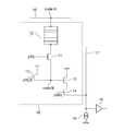
- FIG. 3 is a circuit diagram of a pixel including the photoelectric conversion device according to the present invention.
- the photoelectric conversion device 10 is connected to the common wiring 19 at nodeA.
- the common wiring may be connected to the ground.
- the pixel 18 may include a photoelectric conversion element 10 and a read circuit for reading a signal generated in the photoelectric conversion unit.
- the readout circuit includes, for example, a transfer transistor 11 electrically connected to the photoelectric conversion element, an amplification transistor 13 having a gate electrode electrically connected to the photoelectric conversion element 10, a selection transistor 14 for selecting a pixel from which information is read, a photoelectric transistor A reset transistor 12 that supplies a reset voltage to the conversion element may be included.
- the transfer transistor 11 may be controlled to transfer by pTX.
- the reset transistor may be controlled in voltage supply by pRES.
- the selection transistor is selected or not selected by pSEL.
- the transfer transistor 11, the reset transistor 12, and the amplifying transistor 13 are connected by nodeB. Depending on the configuration, the transfer transistor may not be provided.
- the reset transistor is a transistor that supplies a voltage for resetting the potential of nodeB.
- the voltage supply can be controlled by applying pRES to the gate of the reset transistor. Depending on the configuration, the reset transistor may not be provided.
- the amplification transistor is a transistor that passes a current corresponding to the potential of nodeB.
- the amplification transistor is connected to a selection transistor 14 that selects a pixel that outputs a signal.
- the selection transistor is connected to the current source 16 and the column output unit 15, and the column output unit 15 may be connected to the signal processing unit.
- the selection transistor 14 is connected to the vertical output signal line 17.
- the vertical output signal line 17 is connected to the current source 16 and the column output unit 15.
- FIG. 4 is a diagram showing an image sensor according to the present invention.
- the imaging element 20 has an imaging region 25 in which a plurality of pixels are two-dimensionally arranged, and a peripheral region 26.
- the area other than the imaging area is a peripheral area.
- the peripheral area has a vertical scanning circuit 21, a readout circuit 22, a horizontal scanning circuit 23, and an output amplifier 24, and the output amplifier is connected to a signal processing unit 27.
- the signal processing unit is a signal processing unit that performs signal processing based on information read by the reading circuit, and examples thereof include a CCD circuit and a CMOS circuit.
- the readout circuit 22 includes, for example, a column amplifier, a CDS circuit, an addition circuit, and the like, and amplifies and adds signals read out from the pixels in the row selected by the vertical scanning circuit 21 through the vertical signal line.
- the column amplifier, the CDS circuit, the addition circuit, and the like are arranged for each pixel column or a plurality of pixel columns, for example.
- the horizontal scanning circuit 23 generates a signal for sequentially reading the signals of the reading circuit 22.
- the output amplifier 24 amplifies and outputs the signal of the column selected by the horizontal scanning circuit 23.
- the above configuration is only one configuration example of the photoelectric conversion device, and the present embodiment is not limited to this.
- the readout circuit 22, the horizontal scanning circuit 23, and the output amplifier 24 are arranged one above the other with the imaging region 25 interposed therebetween so as to constitute two systems of output paths. However, three or more output paths may be provided. Signals output from the output amplifiers are combined as image signals by the signal processing unit.
- the CV measurement sample was prepared by dissolving about 1 mg of the first organic compound in 10 mL of an orthodichlorobenzene solution of 0.1 M tetrabutylammonium perchlorate and performing a deaeration treatment with nitrogen.
- the three-electrode method is used for CV measurement, and each electrode includes a non-aqueous solvent type Ag / Ag + reference electrode, a platinum counter electrode having a diameter of 0.5 mm and a length of 5 cm, and a glassy carbon working electrode having an inner diameter of 3 mm (all BAS Co., Ltd.) was used.
- a model 660C manufactured by ALS, an electrochemical analyzer was used as the electrochemical measuring apparatus. The measurement pulling speed was 0.1 V / s.
- oxidation potential and reduction potential can be estimated from the peak value of the cyclic voltammogram.
- Eox the oxidation potential
- Ered the reduction potential
- Table 1 shows oxidation potentials of exemplary compounds of the first organic compound.
- Example 1 In this example, a photoelectric conversion element was manufactured using a combination of a first organic compound and a second organic compound that satisfy ⁇ E ⁇ 1.5V. Dark current was measured using the produced photoelectric conversion element.
- a photoelectric conversion element was formed on a Si substrate.
- a cathode electrode, an electron block layer, a photoelectric conversion layer, a hole block layer, and an anode electrode are sequentially formed.
- the photoelectric conversion element was manufactured by the following steps.
- a Si substrate was prepared in which a wiring layer and an insulating layer were laminated, and contact holes were formed in the insulating layer from the wiring layer at locations corresponding to the respective pixels so as to be conductive. This contact hole is connected to the pad portion at the end of the substrate by wiring.
- An IZO electrode was formed by a sputtering method so as to overlap this contact hole portion. Patterning was performed to form an IZO electrode (cathode electrode) of 3 mm 2 . At this time, the thickness of the IZO electrode was set to 100 nm.
- An organic compound layer was formed on the IZO electrode by a vacuum deposition method.
- the layer configuration and the layer thickness are as shown in Table 2 below.
- IZO was formed by sputtering as an anode electrode.
- the thickness of the anode electrode was 30 nm.
- Table 2 shows the layer structure of the photoelectric conversion element.
- Table 2 shows the cathode as the lower electrode on the lower side of the table.
- the following compound (d-1) was used for the electron blocking layer.
- the first organic compound of the photoelectric conversion layer is exemplified compounds 1-1 to 3-14, and the hole blocking layer is fullerene C60 (d-2) and C70 (d-3) and the following organic compound (d- Any of 4) was used.
- the characteristics of the photoelectric conversion element were measured and evaluated for the obtained element. When the current when 5 V was applied to the element was confirmed, it was confirmed that the photoelectric conversion element was functioning because the current value in the light place was 10 times or more the current value in the dark place. .
- the probe was held in a constant temperature bath at 60 ° C. and wired to a semiconductor parameter analyzer (Agilent 4155C) and contacted with the electrode.
- a semiconductor parameter analyzer Alignment 4155C
- the criteria for dark current evaluation were as follows. A: 100pA / cm 2 less B: 100pA / cm 2 or more 1000 pA / cm 2 less than C: 1000pA / cm 2 or more 2000 Pa / cm 2 less than D: 2nA / cm 2 or more 10 nA / cm 2 less than E: 10nA / cm 2 or more A to C were good and D and E were bad.
- the dark current evaluation of the photoelectric conversion element of Example 1 was C.
- the area of a 10 ⁇ m square pixel is 1.0 ⁇ 10 ⁇ 6 cm 2 .
- this photoelectric conversion element is used for an image sensor, an image sensor with a low dark current can be obtained. This low dark current characteristic leads to a reduction in noise of the image sensor.
- Examples 2 to 47 A photoelectric conversion element was produced in the same manner as in Example 1 except that the combination of the first organic compound and the second organic compound was the combination shown in Table 4. The results of Examples 1 to 47 are shown in Table 4 below.
- a photoelectric conversion element was produced in the same manner as in Example 1 except that the combination of the first organic compound and the second organic compound was changed to the combination shown in Table 5.
- the combination of the compounds in Table 5 is a combination of ⁇ E ⁇ 1.5V.
- the produced photoelectric conversion element was evaluated for dark current by the same measurement method as in Example 1.
- a photoelectric conversion element having ⁇ E of 1.5 V or higher was a result of evaluation C or higher for the dark current of any combination of elements, and low dark current characteristics were obtained.
- Example 48 Table 6 shows the changes in dark current when the compound concentration of Example Compound 1-7 used in Example 2 was changed from 20 wt% to 30 wt% by 2.5 wt%.
- the concentration of the first organic compound is preferably less than 35% by weight and more preferably 27.5% by weight or less.
- the lower limit concentration is not limited in the present invention, and may be a concentration at which a necessary absorption rate can be obtained, for example.
- Examples 49-52, Comparative Example 17 A photoelectric conversion element was produced in the same manner as in Example 1 except that the constituent materials and the layer thicknesses were changed to Table 7.
- the exemplified compounds shown in Table 8 and the following comparative compound (e-1) were used as the first organic compound.
- Table 7 it is described as the first organic compound.
- the dark current of each element was measured and relative evaluation was performed.
- the structure of comparative compound (e-1) is as follows. The oxidation potential of compound e-1 was 0.92V.
- Example 53 Comparative Example 18
- the maximum absorption peak wavelength refers to the wavelength of the peak having the largest absorption coefficient.
- a chloroform solution containing the first organic compound in mol / L was prepared, and the absorption spectrum was measured with a spectrophotometer (JASCO Ubest-550). From the measurement results, obtain the maximum absorption peak wavelength and absorbance.
- the molar extinction coefficient was determined from the absorbance according to the Lambert-Beer rule.
- the compound represented by the general formula [28] can obtain an absorption peak suitable for obtaining a panchromatic absorption band in the visible region and a strong absorption having a molar extinction coefficient of 40000 or more. I understand. Strong absorption is an important factor for a photoelectric conversion element because it leads to a high external quantum yield.
- Example 54 A photoelectric conversion element was produced in the same manner as in Example 1 except that a silicon nitride layer formed by CVD was used as the sealing layer.
- the silicon nitride layer was formed with a layer thickness of 1 ⁇ m.
- the device was irradiated with 365 nm LED light at an intensity of 1 W / cm 2 for 24 hours to evaluate durability.
- the absorption rate of 365 nm of the formed SiN (1 ⁇ m) was 75%.
- the dark current value of this element did not change even after 24 hours.
- the dark current of the photoelectric conversion element produced in Example 1 increased by about 10% after 24 hours of light irradiation. This is because the glass cap absorbs ultraviolet rays smaller than SiN. Considering this, it is preferable to provide the sealing layer with a material capable of absorbing ultraviolet rays.
- FIG. 6 is an Arrhenius plot of the photoelectric conversion element of Example 1.
- the vertical axis represents the dark current value normalized by the dark current value at 60 ° C.
- the scale on the vertical axis is the common logarithm.
- the horizontal axis is the reciprocal of absolute temperature.
- the absolute value of the inclination increases from around 60 ° C. toward the high temperature side.
- the activation energy was determined from this slope according to the following equation (5).
- T absolute temperature
- k B Boltzmann constant
- E a activation energy
- J current value at temperature T
- J 0 frequency factor. From this slope, the activation energy of the dark current was determined to be 0.84 eV.
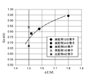
- FIG. 7 shows the activation energy obtained for the photoelectric conversion elements fabricated in Examples 2, 6, 12, 34, and Comparative Example 6 in the same manner as in Example 55, and plotted against the corresponding ⁇ E. is there. It can be seen that the activation energy increases as ⁇ E increases. FIG. 7 shows that the activation energy is large when ⁇ E is 1.5 V or more. This means that when ⁇ E is 1.5 V or more, the charge generation probability due to thermal excitation decreases.
- Table 10 shows the relationship between activation energy and dark current evaluation. As shown in the table, when the activation energy is 0.70 eV or more, the dark current is evaluated as C or more.
- the dark current activation energy is preferably 0.70 eV or more in order to reduce the dark current.
- the photoelectric conversion element according to the present invention is a photoelectric conversion element with reduced dark current.
- An image pickup device having this is preferable because there is little dark current noise derived from the photoelectric conversion element portion.
Landscapes
- Engineering & Computer Science (AREA)
- Physics & Mathematics (AREA)
- Electromagnetism (AREA)
- Power Engineering (AREA)
- Multimedia (AREA)
- Signal Processing (AREA)
- Condensed Matter Physics & Semiconductors (AREA)
- General Physics & Mathematics (AREA)
- Computer Hardware Design (AREA)
- Microelectronics & Electronic Packaging (AREA)
- Light Receiving Elements (AREA)
- Solid State Image Pick-Up Elements (AREA)
Abstract
アノードと、カソードと、前記アノードと前記カソードとの間に配置されている光電変換層と、を有する光電変換素子であって、前記光電変換層は第一の有機化合物と第二の有機化合物とを有し、前記第一の有機化合物の酸化電位は、前記第二の有機化合物の酸化電位よりも小さく、下記式(A)であらわされるΔEが、下記式(B)を満たし、ΔE=第一の有機化合物の酸化電位-第二の有機化合物の還元電位(A) ΔE≧1.5 [V](B)前記第一の有機化合物は、下記一般式[1]、フルオランテン誘導体、金属錯体のいずれかであることを特徴とする光電変換素子を提供する。R1は水素原子または置換基を表す。Ar1、Ar2、Z1は置換基を表す。n1及びn2は0乃至4までの整数を表す。X1乃至X3は窒素原子、硫黄原子、酸素原子または炭素原子を表す。
Description
本発明は、光電変換素子、撮像素子および撮像装置に関する。
近年、有機化合物を光電変換層に用い、信号読み出し用基板上に形成した構造を有する固体撮像素子の開発が進んでいる。
光電変換素子における暗電流を改善するために、様々な構成が知られている。特許文献1には、光電変換層とアノードとの間に電子ブロック層を設け、光電変換層と電子ブロック層とのエネルギー準位の関係および電子ブロック層の層厚を規定することで暗電流を低減する有機光電変換素子が記載されている。
特許文献2には、光電変換層とカソードとの間に正孔ブロック層を設け、光電変換層と正孔ブロック層とのエネルギー準位の関係を規定することで暗電流を低減する有機光電変換素子が記載されている。
光電変換素子における暗電流には、アノードやカソードから流れ込む電流のほかに、光電変換層内から発生する暗電流が存在する。
特許文献1および2には、光電変換層内のp型有機半導体材料とn型有機半導体材料の間で発生する暗電流は記載も示唆もされておらず、光電変換素子の暗電流の低減が不十分であった。
そこで本発明は、光電変換素子における光電変換層内のp型有機半導体材料とn型有機半導体材料の間で発生する暗電流を低減した有機光電変換素子を提供することを目的とする。
本発明の一態様は、アノードと、カソードと、前記アノードと前記カソードとの間に配置されている光電変換層とを有する光電変換素子であって、前記光電変換層は第一の有機化合物と第二の有機化合物とを有し、前記第一の有機化合物の酸化電位は、前記第二の有機化合物の酸化電位よりも小さく、下記式(A)であらわされるΔEが、下記式(B)を満たし、
ΔE=第一の有機化合物の酸化電位-第二の有機化合物の還元電位 (A)
ΔE≧1.5 [V] (B)
前記第一の有機化合物が下記一般式[1]乃至[5]のいずれかであることを特徴とする光電変換素子を提供する。
ΔE=第一の有機化合物の酸化電位-第二の有機化合物の還元電位 (A)
ΔE≧1.5 [V] (B)
前記第一の有機化合物が下記一般式[1]乃至[5]のいずれかであることを特徴とする光電変換素子を提供する。

一般式[1]において、R1は水素原子、ハロゲン原子、置換あるいは無置換のアルキル基、置換あるいは無置換のアルコキシ基、置換あるいは無置換のアリール基、置換あるいは無置換の複素環基、置換あるいは無置換のビニル基、置換あるいは無置換のアミノ基、シアノ基を表す。
n1及びn2は0乃至4までの整数を表す。X1乃至X3は窒素原子、硫黄原子、酸素原子または炭素原子を表わし、当該炭素原子は、置換基を有してもよい。
Ar1及びAr2は置換あるいは無置換のアリール基、または置換あるいは無置換の複素環基からそれぞれ独立に選ばれる。
Ar1及びAr2が複数ある場合はそれぞれ同じでも異なってもよく、Ar1及びAr2はX2あるいはX3が炭素原子の場合、互いに結合して環を形成してもよい。
Z1はハロゲン原子、シアノ基、置換あるいは無置換のヘテロアリール基または以下の一般式[1-1]乃至[1-9]で表される置換基のいずれかを表す。
一般式[1-1]乃至[1-9]において、R521乃至R588は水素原子、ハロゲン原子、置換あるいは無置換のアルキル基、置換あるいは無置換のアルコキシ基、置換あるいは無置換のアリール基、置換あるいは無置換の複素環基、置換あるいは無置換のビニル基、置換あるいは無置換のアミノ基、シアノ基からそれぞれ独立に選ばれる。

一般式[2]においてR20乃至R29は水素原子、ハロゲン原子、置換あるいは無置換のアルキル基、置換あるいは無置換のアルコキシ基、置換あるいは無置換のアリール基、置換あるいは無置換の複素環基、置換あるいは無置換のビニル基、置換あるいは無置換のアミノ基、シアノ基からそれぞれ独立に選ばれる。R20乃至R29のうちの隣り合う2つは互いに結合して環を形成してもよい。

一般式[3]乃至[5]において、Mは金属原子を表す。当該金属原子は酸素原子またはハロゲン原子を置換基として有してもよい。
L1乃至L9は金属Mに配位する配位子を表す。当該配位子は、置換あるいは無置換のアリール基、置換あるいは無置換の複素環基からなり、それぞれL1乃至L9のうちの隣り合う2つは互いに結合して環を形成してもよい。
また、本発明の別の態様では、アノードと、カソードと、前記アノードと前記カソードとの間に配置されている光電変換層とを有する光電変換素子であって、暗電流の活性化エネルギーが0.70eV以上であることを特徴とする光電変換素子を提供する。
本発明によれば、暗電流が低減された光電変換素子を提供することができる。
本発明は、有機化合物からなる光電変換層を有する光電変換素子の暗電流の低減に関する。光電変換層が有する2種類の有機化合物のエネルギー差を一定以上とすることで暗電流を低減することができる。
また、光電変換素子の暗電流の活性化エネルギーを一定以上とすることで、暗電流を低減することができる。
熱的な電荷分離による暗電流は、活性化エネルギーが高いほど発生しにくくなる。活性化エネルギーは、第一の有機化合物と、第二の有機化合物とが電荷分離した状態に励起されるためのエネルギーの大きさである。活性化エネルギー以上のエネルギーを熱エネルギーが与えた場合、暗電流の原因となる。
本発明の一態様は、暗電流の活性化エネルギーを0.70eV以上とすることで、暗電流が低減された光電変換素子である。暗電流の活性化エネルギーは、0.75eV以上がより好ましく、0.80eV以上がさらに好ましい。
[光電変換素子の構成]
本実施形態においては、アノードとカソードとの間に有機化合物からなる光電変換層を有する光電変換素子を例に挙げて説明する。
本実施形態においては、アノードとカソードとの間に有機化合物からなる光電変換層を有する光電変換素子を例に挙げて説明する。
本発明に係る光電変換素子が有する光電変換層は、光を受け、その光量に応じた電荷を発生する層である。光電変換層の機能は、光を吸収することで正孔と電子に電荷分離を行い、光を電気信号に変換することである。光電変換層は、複数種類の有機化合物を有してもよい。光電変換層内に正の電荷を運ぶドナー材料と負の電荷を運ぶアクセプター材料がランダムに混ざった層はバルクヘテロジャンクションと呼ばれる。
光電変換層が複数種類の有機化合物を有する場合、複数種類の有機化合物が1つの層に混合されてもよいし、複数種類の有機化合物が、複数の層に含まれてもよい。
光電変換層は、p型有機半導体又はn型有機半導体を含有した層であることが好ましく、有機p型化合物と、有機n型化合物とを混合したバルクへテロ層を少なくとも一部に含むことがより好ましい。ヘテロ層は混合層と言い換えることもできる。
バルクへテロ層を有する光電変換層は、光電変換効率が高い。さらに、混合比率が適切なバルクへテロ層においては、光電変換層の電子移動度および正孔移動度が高いので、光電変換素子の光応答速度が高い。したがって、最適な混合比率のバルクヘテロ層を有することが好ましい。
[ΔEについて]
ΔEは下記式(A)にて定義されるエネルギーギャップである。
ΔE=第一の有機化合物の酸化電位-第二の有機化合物の還元電位 (A)
またΔEは、下記式(B)を満たす。
ΔE≧1.5 [V] (B)
ΔEは下記式(A)にて定義されるエネルギーギャップである。
ΔE=第一の有機化合物の酸化電位-第二の有機化合物の還元電位 (A)
またΔEは、下記式(B)を満たす。
ΔE≧1.5 [V] (B)
図1は、ΔEを表すエネルギー図である。第一の有機化合物の酸化電位は第一の有機化合物のHOMOに相当する。また第二の有機化合物の還元電位は第二の有機化合物のLUMOに相当する。酸化還元電位は溶液中の分子と電極間でのポテンシャルエネルギー差であり、分子単独の物性値である。
暗電流は、p型有機半導体材料からn型有機半導体材料へ熱的な電荷分離により発生する場合がある。ΔEは、熱的な電荷分離による暗電流が発生するために必要なエネルギーという意味がある。
式(B)を満たすことで、光励起ではなく、熱励起による電荷分離による、暗電流が発生することを抑制することができる。
それは、ΔEの大きさが、暗電流発生の活性化エネルギーに相関している、より具体的には、ΔEが大きいほど、暗電流の活性化エネルギーが大きくなる傾向があるからである。式(B)を満たすことで、暗電流発生の活性化エネルギーを大きくし、熱励起による暗電流発生を抑えることで暗電流が低減された光電変換素子を得ることができる。
また熱励起による暗電流においては、バルクヘテロジャンクションを形成するp型有機半導体とn型有機半導体の分子同士が接触していることが原因である。
式(B)に加えて、光電変換層が他の分子との接触が抑制された有機化合物または熱電子の発生を抑制する有機化合物を有することで、活性化エネルギーを大きくし、暗電流を低減できる。
本発明に係る光電変換素子は、光電変換層が第一の有機化合物と第二の有機化合物を有し、第一の有機化合物が他分子との接触を抑制する性質または熱電子の発生を抑制する性質を有するため、暗電流が低減された光電変換素子である。
光電変換層は、第一の有機化合物と第二の有機化合物とを有し、第一の有機化合物は電子ドナー材料である。
第一の有機化合物は、光電変換層が有するp型有機半導体である。第一の有機化合物は、ドナー性有機半導体であり、電子を供与しやすい性質がある。具体的には2つの有機化合物のうち酸化電位が小さい方が第一の有機化合物である。つまり第一の有機化合物は電子ドナー材料、第二の有機化合物は電子アクセプター材料である。
第一の有機化合物は、例えば、トリアリールアミン化合物、ピラン化合物、キナクリドン化合物、ベンジジン化合物、ピラゾリン化合物、スチリルアミン化合物、ヒドラゾン化合物、トリフェニルメタン化合物、カルバゾール化合物、ポリシラン化合物、チオフェン化合物、フタロシアニン化合物、シアニン化合物、メロシアニン化合物、オキソノール化合物、ポリアミン化合物、インドール化合物、ピロール化合物、ピラゾール化合物、ポリアリーレン化合物、縮合芳香族炭素環化合物(ナフタレン誘導体、アントラセン誘導体、フェナントレン誘導体、テトラセン誘導体、ピレン誘導体、ペリレン誘導体、フルオランテン誘導体)、含窒素ヘテロ環化合物を配位子として有する金属錯体等を用いることができる。中でも、トリアリールアミン化合物、ピラン化合物、キナクリドン化合物、ピロール化合物、フタロシアニン化合物、メロシアニン化合物、縮合芳香族炭素環化合物が好ましい。
フルオランテン誘導体とは、化学構造式中にフルオランテン骨格を有する化合物である。フルオランテン骨格に縮環が付加された化合物も含むものである。すなわち、化学構造式からフルオランテン骨格が見出される化合物を意味する。他のナフタレン誘導体、アントラセン誘導体、フェナントレン誘導体、テトラセン誘導体、ピレン誘導体、ペリレン誘導体についても同様である。
第一の有機化合物は、吸収波長が450nm以上700nm以下の可視域にあることが好ましい。光電変換層がパンクロマティックな吸収帯を得るためには、吸収ピーク波長が、500nm以上であることが好ましい。特に530nm以上であることが好ましく、530nm以上650nm以下であることがさらに好ましい。当該領域に吸収ピーク波長を有することは、近接する領域である、450nm以上470nm以下の青領域や600nm以上630nm以下の赤領域にも吸収を有するので、パンクロマティック性が向上する。
吸収ピーク波長は、クロロホルム溶液中の吸収スペクトルを測定する等で得ることができる。
また、式(B)を満たすことや暗電流の活性化エネルギーが一定以上であることは、第一の有機化合物の吸収ピーク波長が530nm以上である場合に、特に好ましい。
吸収ピーク波長が530nm以上である有機化合物は、バンドギャップが比較的小さい有機化合物である。バンドギャップが小さい有機化合物は、そのHOMOが第二の有機化合物のLUMOと近くなってしまう傾向がある。すなわち、暗電流が発生しやすくなる。その場合に、式(B)を満たすことや暗電流の活性化エネルギーが一定以上であることを満たすことで特に大きな効果を奏するものである。
光電変換層内における第一の有機化合物の濃度は、第一の有機化合物と第二の有機化合物との合計を100重量%とした場合に、35重量%未満であることが好ましい。より好ましくは27.5重量%以下であることが好ましい。第一の有機化合物の濃度が好ましい範囲にある場合、暗電流をさらに低減できるので好ましい。
第一の有機化合物は、下記一般式[1]乃至[5]のいずれかである。第一の有機化合物は一般式[1]で表される有機化合物であることが特に好ましい。

一般式[1]において、R1は水素原子、ハロゲン原子、置換あるいは無置換のアルキル基、置換あるいは無置換のアルコキシ基、置換あるいは無置換のアリール基、置換あるいは無置換の複素環基、置換あるいは無置換のビニル基、置換あるいは無置換のアミノ基、シアノ基を表す。
n1及びn2は0乃至4までの整数を表す。
X1乃至X3は窒素原子、硫黄原子、酸素原子または炭素原子を表し、当該炭素原子は、置換基を有してもよい。
Ar1及びAr2は置換あるいは無置換のアリール基、または置換あるいは無置換の複素環基からそれぞれ独立に選ばれる。Ar1及びAr2が複数ある場合はそれぞれ同じでも異なってもよく、Ar1及びAr2はX2あるいはX3が炭素原子の場合、互いに結合して環を形成してもよい。
Z1はハロゲン原子、シアノ基、置換あるいは無置換のヘテロアリール基または以下の一般式[1-1]乃至[1-9]で表される置換基のいずれかを表す。
一般式[1-1]乃至[1-9]において、R521乃至R588は水素原子、ハロゲン原子、置換あるいは無置換のアルキル基、置換あるいは無置換のアルコキシ基、置換あるいは無置換のアリール基、置換あるいは無置換の複素環基、置換あるいは無置換のビニル基、置換あるいは無置換のアミノ基、シアノ基からそれぞれ独立に選ばれる。

一般式[1]で表される有機化合物の中でも、Ar1が置換あるいは無置換のアリール基、または置換あるいは無置換の複素環基であることが好ましい。当該複素環基の複素原子は窒素であることが好ましい。X1が硫黄または酸素原子であることが好ましい。n1は1であり、n2は0であることが好ましい。Ar2はn2が0であるため、単結合を表す。
第一の有機化合物は、下記一般式[2]であってもよい。
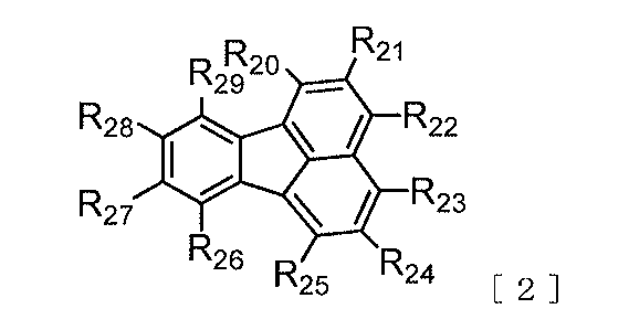
一般式[2]においてR20乃至R29は水素原子、ハロゲン原子、置換あるいは無置換のアルキル基、置換あるいは無置換のアルコキシ基、置換あるいは無置換のアリール基、置換あるいは無置換の複素環基、置換あるいは無置換のビニル基、置換あるいは無置換のアミノ基、シアノ基からそれぞれ独立に選ばれる。R20乃至R29のうちの隣り合う2つは互いに結合して環を形成してもよい。
第一の有機化合物は、下記一般式[3]乃至[5]のいずれかであってもよい。

一般式[3]乃至[5]において、Mは金属原子を表す。当該金属原子は酸素原子またはハロゲン原子を置換基として有してもよい。
L1乃至L9は金属Mに配位する配位子を表す。当該配位子は、置換あるいは無置換のアリール基、置換あるいは無置換の複素環基からなり、それぞれL1乃至L9のうちの隣り合う2つは互いに結合して環を形成してもよい。
ここで環を形成するとは、形成する環構造を限定しない。例えば、5員環を縮環させても、6員環を縮環させても、7員環を縮環させてもよい。縮環する環構造は、芳香環であっても、脂環構造であってもよい。以下本明細書において、環を形成してよいとは、特に言及しない限り同じ意味で用いられる。
一般式[3]乃至[5]において、Mがイリジウムである場合は、6配位錯体であることが好ましい。Mがプラチナ、バナジウム、コバルト、ガリウム、チタンである場合は、4配位錯体であることが好ましい。当該配位数とすることで錯体の安定性が高いためである。
一般式[2]は、より具体的には以下の一般式[11]乃至[27]のいずれかで表すことができる。


一般式[11]乃至[27]において、R31乃至R390は水素原子、ハロゲン原子、置換あるいは無置換のアルキル基、置換あるいは無置換のアルコキシ基、置換あるいは無置換のアリール基、置換あるいは無置換の複素環基、置換あるいは無置換のビニル基、置換あるいは無置換のアミノ基、シアノ基からそれぞれ独立に選ばれる。
上記一般式[1]及び[2]、一般式[1-1]乃至[1-9]、一般式[11]乃至[27]の置換基の具体例を以下に示す。
ハロゲン原子としては、塩素原子、臭素原子、ヨウ素原子が挙げられ、フッ素原子であることが好ましい。
アルキル基は、炭素原子数1乃至10のアルキル基が好ましい。例えば、メチル基、エチル基、ノルマルプロピル基、イソプロピル基、ノルマルブチル基、ターシャリブチル基、セカンダリブチル基、オクチル基、1-アダマンチル基、2-アダマンチル基などが挙げられる。アルキル基は、炭素原子数1乃至4のアルキル基であってもよい。
アルコキシ基は、炭素原子数1乃至10のアルコキシ基が好ましい。例えば、メトキシ基、エトキシ基、ノルマルプロピオキシ基、イソプロピオキシ基、ノルマルブトキシ基、ターシャリブトキシ基、セカンダリブトキシ基、オクトキシ基などが挙げられる。アルコキシ基は炭素原子数1乃至4のアルコキシ基であってもよい。
アリール基は、炭素原子数6乃至20のアリール基が好ましい。例えば、フェニル基、ナフチル基、インデニル基、ビフェニル基、ターフェニル基、フルオレニル基、アントラセニル基、ピレニル基、フルオランテニル基、ペリレニル基などが挙げられ。特に、フェニル基、ビフェニル基、ターフェニル基、フルオレニル基、ナフチル基が分子量は低く、化合物の昇華性を考慮すると好ましい。
複素環基は、炭素原子数3乃至15の複素環基が好ましい。例えば、ピリジル基、ピラジル基、トリアジル基、チエニル基、フラニル基、ピロリル基、オキサゾリル基、オキサジアゾリル基、チアゾリル基、チアジアゾリル基、カルバゾリル基、アクリジニル基、フェナントロリル基、ベンゾチオフェニル基、ジベンゾチオフェニル基、ベンゾチアゾリル基、ベンゾアゾリル基、ベンゾピロリル基などが挙げられる。複素環基が有する複素原子は、窒素が好ましい。
アミノ基は、アルキル基、アリール基を置換基として有するアミノ基が好ましい。例えば、N-メチルアミノ基、N-エチルアミノ基、N,N-ジメチルアミノ基、N,N-ジエチルアミノ基、N-メチル-N-エチルアミノ基、N-ベンジルアミノ基、N-メチル-N-ベンジルアミノ基、N,N-ジベンジルアミノ基、アニリノ基、N,N-ジフェニルアミノ基、N,N-ジナフチルアミノ基、N,N-ジフルオレニルアミノ基、N-フェニル-N-トリルアミノ基、N,N-ジトリルアミノ基、N-メチル-N-フェニルアミノ基、N,N-ジアニソリルアミノ基、N-メシチル-N-フェニルアミノ基、N,N-ジメシチルアミノ基、N-フェニル-N-(4-ターシャリブチルフェニル)アミノ基、N-フェニル-N-(4-トリフルオロメチルフェニル)アミノ基等が挙げられる。アミノ基が置換基として有するアルキル基やアリール基は、上記の置換基の例示で示された通りである。
一般式[1]及び[2]、一般式[1-1]乃至[1-9]、一般式[11]乃至[27]におけるアルキル基、アリール基、複素環基、アミノ基、ビニル基、アリール基が有する置換基は以下の置換基が挙げられる。当該置換基は、メチル基、エチル基、プロピル基、ブチル基などの炭素原子数1乃至4のアルキル基、ベンジル基などのアラルキル基、フェニル基、ビフェニル基などのアリール基、ピリジル基、ピロリル基などの窒素原子を複素原子とする複素環基、ジメチルアミノ基、ジエチルアミノ基、ジベンジルアミノ基、ジフェニルアミノ基、ジトリルアミノ基などのアミノ基、メトキシル基、エトキシル基、プロポキシル基、フェノキシル基などのアルコキシル基、1,3-インダンジオニル基、5,-フルオロ-1,3-インダンジオニル基、5,6-ジフルオロ-1,3-インダンジオニル基、5,6-ジシアノ-1,3-インダンジオニル基、5-シアノ-1,3-インダンジオニル基、シクロペンタ[b]ナフタレン-1,3(2H)-ジオニル基、フェナレン-1,3(2H)-ジオニル基、1,3-ジフェニル-2,4,6(1H,3H,5H)-ピリミジントリオニル基などの環状ケトン基、シアノ基、ハロゲン原子などが挙げられる。ハロゲン原子はフッ素、塩素、臭素、ヨウ素などであり、フッ素原子が好ましい。
一般式[3]乃至[5]について配位子L1乃至L9の具体例を以下に示す。
配位子L1乃至L9は置換あるいは無置換のアリール基と置換あるいは無置換の複素環基から選ばれる置換基を複数結合させた配位子である。
配位子を構成するアリール基として、フェニル基、ナフチル基、インデニル基、ビフェニル基、ターフェニル基、フルオレニル基、アントラセニル基、ピレニル基、フルオランテニル基、ペリレニル基などが挙げられるが、もちろんこれらに限定されるものではない。
配位子を構成する複素環基として、ピリジル基、ピラジル基、トリアジル基、チエニル基、フラニル基、ピロリル基、オキサゾリル基、オキサジアゾリル基、チアゾリル基、チアジアゾリル基、カルバゾリル基、アクリジニル基、フェナントロリル基、ベンゾチオフェニル基、ジベンゾチオフェニル基、ベンゾチアゾリル基、ベンゾアゾリル基、ベンゾピロリル基などが挙げられるが、もちろんこれらに限定されるものではない。
一般式[3]乃至[5]における配位子が有する置換基、即ちアリール基及び複素環基が有する置換基は、メチル基、エチル基、プロピル基、ブチル基などの炭素原子数1乃至4のアルキル基、ベンジル基などのアラルキル基、フェニル基、ビフェニル基などのアリール基、ピリジル基、ピロリル基などの窒素原子を複素原子とする複素環基、ジメチルアミノ基、ジエチルアミノ基、ジベンジルアミノ基、ジフェニルアミノ基、ジトリルアミノ基などのアミノ基、メトキシル基、エトキシル基、プロポキシル基、フェノキシル基などのアルコキシル基、1,3-インダンジオニル基、5,-フルオロ-1,3-インダンジオニル基、5,6-ジフルオロ-1,3-インダンジオニル基、5,6-ジシアノ-1,3-インダンジオニル基、5-シアノ-1,3-インダンジオニル基、シクロペンタ[b]ナフタレン-1,3(2H)-ジオニル基、フェナレン-1,3(2H)-ジオニル基、1,3-ジフェニル-2,4,6(1H,3H,5H)-ピリミジントリオニル基などの環状ケトン基、シアノ基、ハロゲン原子などが挙げられる。ハロゲン原子はフッ素、塩素、臭素、ヨウ素などであり、フッ素原子が好ましい。
配位子は、ヒドロキシ基やカルボキシル基等を置換基として有し、ヒドロキシ基やカルボキシル基を介して金属原子結合してもよい。
一般式[1]は、下記の一般式[28]で表される構造を有することが好ましい。
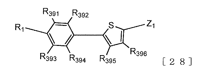
R391乃至R396は水素原子、ハロゲン原子、置換あるいは無置換のアルキル基、置換あるいは無置換のアルコキシ基、置換あるいは無置換のアリール基、置換あるいは無置換の複素環基、置換あるいは無置換のビニル基、置換あるいは無置換のアミノ基、シアノ基からそれぞれ独立に選ばれる。R391乃至R396のうちの隣接する2つは、互いに結合して環を形成してもよい。特にR394とR395とが結合して環を形成するのが好ましい。
また一般式[28]で表される有機化合物は、吸収ピーク波長が522nm以上600nm以下において強い吸収を持つ材料である。この波長領域に吸収ピークを有するとは、前述の通り、光電変換層がパンクロマティック性を有するために好ましい。
以下に第一の有機化合物の具体例を示す。


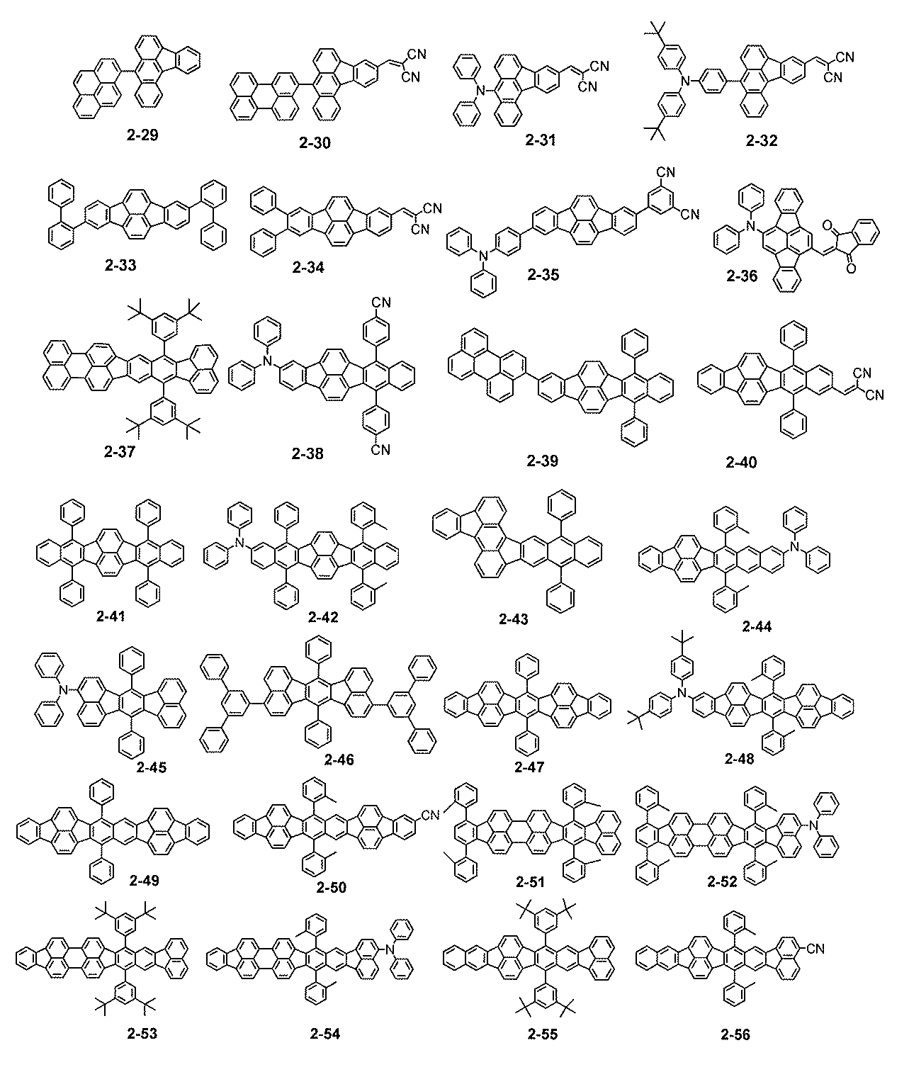
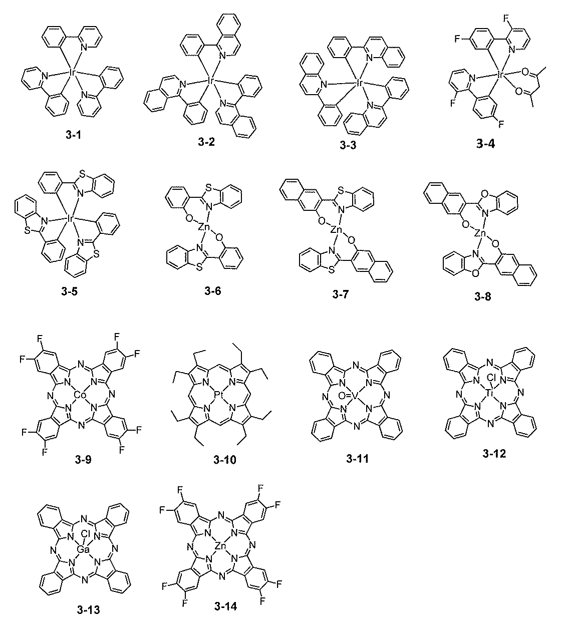
例示化合物1-1乃至1-24は、含硫黄原子を含む5員環複素環基を中心に持つ化合物群である。当該複素環基を有し、Z1が電子吸引性の置換基である化合物は、化合物のHOMO準位が低い化合物である。その結果、ΔEを大きくすることができ、暗電流の原因となる熱電子の発生が抑制される。
例示化合物1-1乃至1-24の中でも、Ar1またはAr2を有する有機化合物は、排除体積が大きくなるので、他の分子との接触の確率が低い。このためアクセプター材料が近づきづらくなり、熱励起による電子の受け渡しが発生しにくい。このため、暗電流を低減できる。
例示化合物2-1乃至2-56は、フルオランテン骨格を中心に持つ化合物群である。フルオランテン骨格は電子吸引性であるので暗電流の原因となる熱電子の発生が抑制されるため、第一の有機化合物として好ましい。
例示化合物3-1乃至3-14は、金属原子を中心とする錯体化合物群である。各配位子には電子吸引性を持つ部位として複素環化合物が含まれることで暗電流の原因となる熱電子の発生が抑制されるため、第一の有機化合物として好ましい。
第一の有機化合物は、酸化電位が0.65V以上であることが好ましい。
光電変換層は、第二の有機化合物としてフラーレンまたはフラーレン誘導体を有してよい。フラーレンまたはフラーレン誘導体はn型有機半導体として機能してよい。
フラーレンまたはフラーレン誘導体分子が光電変換層において連なることで、電子の輸送経路が形成される。そのため、電子輸送性が向上し、光電変換素子の高速応答性が向上する。
フラーレンまたはフラーレン誘導体の含有量は、第一の有機化合物と第二の有機化合物との合計を100重量%とした場合、光電変換効率を考慮すると、40重量%以上85重量%以下であってよい。
フラーレンまたはフラーレン誘導体は、例えば、フラーレンC60、フラーレンC70、フラーレンC76、フラーレンC78、フラーレンC80、フラーレンC82、フラーレンC84、フラーレンC90、フラーレンC96、フラーレンC240、フラーレン540、ミックスドフラーレン、フラーレンナノチューブ等が挙げられる。
フラーレン誘導体は、置換基を有してもよい。この置換基は、アルキル基、アリール基、複素環基があげられる。
フラーレン誘導体は、フラーレンC60が好ましい。
光電変換層は、非発光であることが好ましい。非発光とは、可視光領域(波長400nm~730nm)において発光量子効率が1%以下、好ましくは0.5%以下、より好ましくは0.1%以下である。光電変換層の発光量子効率が1%以内であれば、センサや撮像素子に適用した場合であっても、センシング性能又は撮像性能に与える影響が小さいため、撮像素子として好ましい。
本発明に係る光電変換素子は、アノード電極と光電変換層との間にさらに正孔ブロック層を有してもよい。正孔ブロック層は、アノード電極から光電変換層へ正孔が流れ込むことを抑制する層であり、イオン化ポテンシャルが高いことが好ましい。
本発明に係る光電変換素子は、カソード電極と光電変換層との間にさらに電子ブロック層を有してもよい。電子ブロック層は、カソード電極から光電変換層へ電子が流れ込むことを抑制する層であり、電子親和力あるいはLUMO(最低非占有軌道エネルギー)が小さいことが好ましい。
図2は、本実施形態に係る光電変換素子の一例を示す断面模式図である。光電変換素子には、光を電荷に変換する光電変換層1が、一対の電極である、アノード電極4とカソード電極5との間に配置されている。アノード電極の上には保護層7、波長選択部8、マイクロレンズ9が配置されている。カソード電極には、読み出し回路6が接続されている。
一対の電極のうち基板に近い電極を下部電極と呼び、基板から遠い電極を上部電極と呼ぶことがある。下部電極はアノード電極であっても、カソード電極であってもよい。下部電極は、反射率が高い電極であってよい。電極が反射率の高い材料で構成されてもよいし、電極層に加えて反射層を有してもよい。
本発明に係る光電変換素子は、基板を有してよい。基板は、例えば、シリコン基板、ガラス基板、フレキシブル基板等を用いることができる。
本発明に係る光電変換素子が有するカソード電極は、光電変換層で発生した電荷のうちの正孔を捕集する電極である。一方、アノード電極は、光電変換層で発生した電荷のうち電子を捕集する電極である。カソード電極およびアノード電極を構成する材料は導電性が高く、透明性を有していれば制限されない。カソード電極とアノード電極とを構成する材料は同じであっても異なってもよい。
電極の材料は、具体的には、金属、金属酸化物、金属窒化物、金属硼化物、有機導電性化合物、これらの混合物等が挙げられ、更に具体的には、アンチモンやフッ素等をドープした酸化錫(ATO、FTO)、酸化錫、酸化亜鉛、酸化インジウム、酸化インジウム錫(ITO)、酸化亜鉛インジウム(IZO)等の導電性金属酸化物、金、銀、クロム、ニッケル、チタン、タングステン、アルミ等の金属及びこれらの金属の酸化物や窒化物などの導電性化合物(一例として窒化チタン(TiN)を挙げる)、更にこれらの金属と導電性金属酸化物との混合物又は積層物、ヨウ化銅、硫化銅などの無機導電性物質、ポリアニリン、ポリチオフェン、ポリピロールなどの有機導電性材料、及びこれらとITO又は窒化チタンとの積層物などが挙げられる。電極として特に好ましい材料は、窒化チタン、窒化モリブデン、窒化タンタル、窒化タングステンが挙げられる。
本発明に係る光電変換素子が有する正孔または電子の捕集電極は、光電変換層で発生した電荷のいずれかを捕集する電極である。下部にある捕集電極は、撮像素子の構成においては画素電極であってよい。画素電極がカソードまたはアノードであることは、素子構成や下地の回路構成によって決められる。例えば基板上に基板/アノード電極/光電変換層/カソード電極の順でもよいし、基板/カソード電極/光電変換層/アノード電極の順でもよい。
電極を形成する方法は、電極材料との適正を考慮して適宜選択することができる。具体的には、印刷方式、コーティング方式等の湿式方式、真空蒸着法、スパッタリング法、イオンプレーティング法等の物理的方式、CVD、プラズマCVD法等の化学的方式等により形成することができる。
電極がITOの場合、電子ビーム法、スパッタリング法、抵抗加熱蒸着法、化学反応法(ゾルーゲル法など)、酸化インジウムスズの分散物の塗布などの方法で形成することができる。更に、形成されたITOに、UV-オゾン処理、プラズマ処理などを施すことができる。電極がTiNの場合、反応性スパッタリング法をはじめとする各種の方法が用いられ、更にアニール処理、UV-オゾン処理、プラズマ処理などを施すことができる。
薄膜封止層として特に限定されるものではないが、無機材料により構成される。具体的には、酸化シリコン、窒化シリコン、窒化酸化シリコン、アルミニウム酸化物などがあげられる。酸化シリコン、窒化シリコン、窒化酸化シリコンは、スパッタリング法、CVD法により形成することができ、アルミニウム酸化物は、ALD法(原子層堆積法)により形成することができる。
封止層の封止性能は、水透過率が、10-5g/m2・day以下であればよい。封止層の層厚は特に限定されるものではないが、封止性能の観点から0.5μm以上であることが好ましい。一方で封止性能を保てるならば薄い方がよく、1μm以下であることが特に好ましい。
薄膜封止層が薄い方が好ましい理由は、撮像素子として用いる場合に、光電変換層からのカラーフィルタまでの距離が短いほど混色を低減させる効果があるためである。
光電変換素子を作製する場合は、アニール工程を有することが好ましい。アニール温度は限定されないが、アニール温度の条件は150℃以上190℃以下であってよい。アニール温度は、アニール時間との兼ね合いで適宜決定してされる。
[実施形態に係る撮像素子]
本実施形態に係る撮像素子は、複数の画素を有し、画素は、本発明に係る光電変換素子と、光電変換素子に接続されている読み出しトランジスタを有する。
本実施形態に係る撮像素子は、複数の画素を有し、画素は、本発明に係る光電変換素子と、光電変換素子に接続されている読み出しトランジスタを有する。
複数の画素は、複数の行および複数の列を含む行列に配置されてよい。画素は、それぞれ信号処理回路に接続されてよい。信号処理回路は、各画素からの信号を受け取ることで、画像を得ることができる。
読み出しトランジスタは、光電変換素子において生じた電荷に基づく信号を転送するトランジスタである。
信号処理回路は、CMOSセンサやCCDセンサであってよい。
撮像素子は、光フィルタを、例えばカラーフィルタを有してもよい。光電変換素子が、特定の波長の光に対応している場合、光電変換素子に対応したカラーフィルタを有することが好ましい。カラーフィルタは、1つの受光画素に1つのカラーフィルタを設けても、複数の受光画素に1つのカラーフィルタを設けてもよい。
光フィルタは、カラーフィルタの他にも、赤外線以上の波長を透過するローパスフィルタ、紫外線以下の波長を透過するUVカットフィルタ等があげられる。
撮像素子は、マイクロレンズ等の光学部材を有してもよい。マイクロレンズは、外部からの光を光電変換部に集光するレンズである。マイクロレンズは、1つの受光画素に1つのマイクロレンズを設けてもよいし、複数の受光画素に対応する1つのマイクロレンズを設けてもよい。受光画素が複数設けられている場合は、複数の受光画素のそれぞれに1つずつマイクロレンズが設けられることが好ましい。
本発明に係る撮像素子は、撮像装置に用いることができる。撮像装置は、複数のレンズを有する撮像光学系と、撮像光学系を通過した光を受光する撮像素子と、を有する。また、撮像装置は、撮像素子と、撮像素子を収容する筐体と、を有し、筐体は撮像光学系と接合可能な接合部を有してよい。撮像装置はより具体的には、デジタルカメラまたはデジタルスチルカメラである。
また、撮像装置は、外部からの信号をする受信部をさらに有してもよい。受信部が受信する信号は、撮像装置の撮像範囲、撮像の開始、撮像の終了の少なくともいずれかを制御する信号である。また、撮像装置は、取得した画像を外部に送信する送信部をさらに有してもよい。取得した画像は例えば、撮像した画像、他の機器から送信された画像が挙げられる。
受信部や送信部を有することで、ネットワークカメラとして用いることができる。
図3は、本発明に係る光電変換装置を含む画素の回路図である。光電変換装置10は、nodeAで共通配線19に接続される。共通配線はグランドに接続されてよい。
画素18は、光電変換素子10と、光電変換部で生じた信号を読み出すための読み出し回路を含んでよい。読み出し回路は、例えば光電変換素子と電気的に接続した転送トランジスタ11、光電変換素子10と電気的に接続されたゲート電極を有する増幅トランジスタ13、情報が読み出される画素を選択する選択トランジスタ14、光電変換素子にリセット電圧を供給するリセットトランジスタ12を含んでよい。
転送トランジスタ11は、pTXでその転送を制御されてよい。リセットトランジスタは、pRESで電圧の供給を制御されてよい。選択トランジスタはpSELで選択または非選択の状態となる。
転送トランジスタ11、リセットトランジスタ12、増幅トランジスタ13は、nodeBで接続されている。構成によっては転送トランジスタを有さなくてもよい。
リセットトランジスタはnodeBの電位をリセットする電圧を供給するトランジスタである。リセットトランジスタのゲートにpRESを印加することで電圧の供給を制御できる。構成によってはリセットトランジスタを有さなくてもよい。
増幅トランジスタは、nodeBの電位に応じた電流を流すトランジスタである。増幅トランジスタは信号を出力する画素を選択する選択トランジスタ14に接続されている。選択トランジスタは、電流源16、列出力部15に接続されており、列出力部15は信号処理部に接続されてよい。
選択トランジスタ14は、垂直出力信号線17に接続されている。垂直出力信号線17は、電流源16、列出力部15に接続されている。
図4は、本発明に係る撮像素子を表わす図である。撮像素子20は、複数の画素が2次元に配置されている撮像領域25と、周辺領域26とを有する。撮像領域以外領域は周辺領域である。周辺領域には、垂直走査回路21、読み出し回路22、水平走査回路23、出力アンプ24を有し、出力アンプは信号処理部27に接続されている。信号処理部は、読み出し回路に読みだされた情報により信号処理を行う信号処理部であり、CCD回路、CMOS回路等があげられる。
読み出し回路22は、例えば、列アンプ、CDS回路、加算回路等を含み、垂直走査回路21によって選択された行の画素から垂直信号線を介して読み出された信号に対して増幅、加算等を行う。列アンプ、CDS回路、加算回路等は、例えば、画素列又は複数の画素列毎に配置される。水平走査回路23は、読み出し回路22の信号を順番に読み出すための信号を生成する。出力アンプ24は、水平走査回路23によって選択された列の信号を増幅して出力する。
以上の構成は、光電変換装置の一つの構成例に過ぎず、本実施形態は、これに限定されるものではない。読み出し回路22と水平走査回路23と出力アンプ24とは、2系統の出力経路を構成するため、撮像領域25を挟んで上下に1つずつ配置されている。しかし、出力経路は3つ以上設けられていてもよい。各出力アンプから出力された信号は信号処理部で画像信号として合成される。
[第一の有機化合物の酸化電位の測定]
酸化電位などの電気化学特性の評価は、サイクリックボルタンメトリー(CV)によって行うことができる。
酸化電位などの電気化学特性の評価は、サイクリックボルタンメトリー(CV)によって行うことができる。
CV測定サンプルは、0.1Mテトラブチルアンモニウム過塩素酸塩のオルトジクロロベンゼン溶液10mLに第一の有機化合物を1mg程度溶解させ、窒素による脱気処理を行うことにより調製した。CV測定には三電極法を用い、各電極には、非水溶媒系Ag/Ag+参照電極、直径0.5mm、長さ5cmの白金カウンター電極、内径3mmのガラス状カーボン作用電極(いずれもビー・エー・エス株式会社製)を用いた。電気化学測定装置にはALS社製のモデル660C、電気化学アナライザーを用いた。測定の挿引速度は、0.1V/sとした。図5は、化合物の酸化電位および還元電位を決定するサイクリックボルタモグラムの一例である。サイクリックボルタモグラムのピーク値から酸化電位および還元電位を見積もることができる。本明細書においては、酸化電位はEox、還元電位はEredと記す。
表1は、第一の有機化合物の例示化合物の酸化電位である。

[実施例1]
本実施例では、ΔE≧1.5Vとなる第一の有機化合物と第二の有機化合物との組み合わせを用いて光電変換素子を作製した。作製した光電変換素子を用いて暗電流を測定した。
本実施例では、ΔE≧1.5Vとなる第一の有機化合物と第二の有機化合物との組み合わせを用いて光電変換素子を作製した。作製した光電変換素子を用いて暗電流を測定した。
本実施例において、Si基板の上に光電変換素子を形成した。光電変換素子は、カソード電極、電子ブロック層、光電変換層、正孔ブロック層、アノード電極が順次形成されている。
本実施例において、光電変換素子は以下の工程により作製した。
まず、配線層、絶縁層、が積層されており各画素に対応する箇所に配線層からコンタクトホールが絶縁層に開口を設けて導通可能なように形成されているSi基板を準備した。このコンタクトホールは、基板端のパッド部と配線によって接続されている。このコンタクトホール部に重なるようにIZO電極をスパッタリング法で形成した。パターニングを行い3mm2となるIZO電極(カソード電極)を形成した。このときIZO電極の膜厚を100nmとした。
上記IZO電極上に、有機化合物層を真空蒸着法で形成した。層構成、層厚は下記表2の通りである。次にアノード電極として、IZOをスパッタリング法で形成した。アノード電極の厚さは30nmとした。
光電変換素子の層構成を表2に示す。

なお、表2は、下部電極であるカソードが表の下側になるよう記載したものである。
電子ブロック層には以下の化合物(d-1)を用いた。
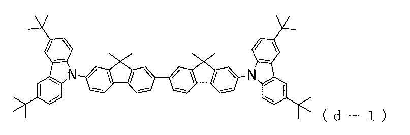
光電変換層の第一の有機化合物には例示化合物1-1乃至3-14、正孔ブロック層にはフラーレンC60(d-2)、およびC70(d-3)と下記の有機化合物(d-4)のいずれかを用いた。

なお、d-2,d-3、d-4の還元電位は表3の通りである。

上部電極を形成後、ガラスキャップと紫外線効果樹脂を使って中空封止を行った。このようにして得られた素子は170℃のホットプレート上で封止面を上向きとして1時間程度アニールした。
得られた素子について、光電変換素子の特性を測定・評価した。素子に5V印加時の電流を確認したところ、いずれの素子でも明所での電流値が暗所での電流値の10倍以上の値であるため光電変換素子が機能していることを確認した。
光電変換素子の暗電流の測定においては、60℃の恒温槽内に保持し半導体パラメータアナライザー(Agilent社4155C)に配線されたプロバーを電極にコンタクトさせて測定した。
暗電流評価の基準は以下の通りとした。
A:100pA/cm2未満
B:100pA/cm2以上1000pA/cm2未満
C:1000pA/cm2以上2000pA/cm2未満
D:2nA/cm2以上10nA/cm2未満
E:10nA/cm2以上
A~Cは良好、D,Eは不良とした。
A:100pA/cm2未満
B:100pA/cm2以上1000pA/cm2未満
C:1000pA/cm2以上2000pA/cm2未満
D:2nA/cm2以上10nA/cm2未満
E:10nA/cm2以上
A~Cは良好、D,Eは不良とした。
実施例1の光電変換素子の暗電流評価はCであった。例えば、10μm角の画素とした場合の面積は1.0×10⁻⁶cm2である。この光電変換素子を撮像素子に用いた場合、低暗電流の撮像素子を得ることができる。この低暗電流特性が撮像素子のノイズの低減につながる。
[実施例2乃至47]
第一の有機化合物及び第二の有機化合物の組み合わせを表4に示す組み合わせとする以外は、実施例1と同様に光電変換素子を作製した。実施例1乃至47の結果を下記表4に示す。
第一の有機化合物及び第二の有機化合物の組み合わせを表4に示す組み合わせとする以外は、実施例1と同様に光電変換素子を作製した。実施例1乃至47の結果を下記表4に示す。

[比較例1乃至16]
第一の有機化合物と第二の有機化合物の組み合わせを表5の組み合わせとする以外は実施例1と同様に光電変換素子を作製した。表5の化合物の組み合わせは、ΔE<1.5Vの組み合わせである。作製した光電変換素子を実施例1と同様の測定法で暗電流評価を行った。
第一の有機化合物と第二の有機化合物の組み合わせを表5の組み合わせとする以外は実施例1と同様に光電変換素子を作製した。表5の化合物の組み合わせは、ΔE<1.5Vの組み合わせである。作製した光電変換素子を実施例1と同様の測定法で暗電流評価を行った。
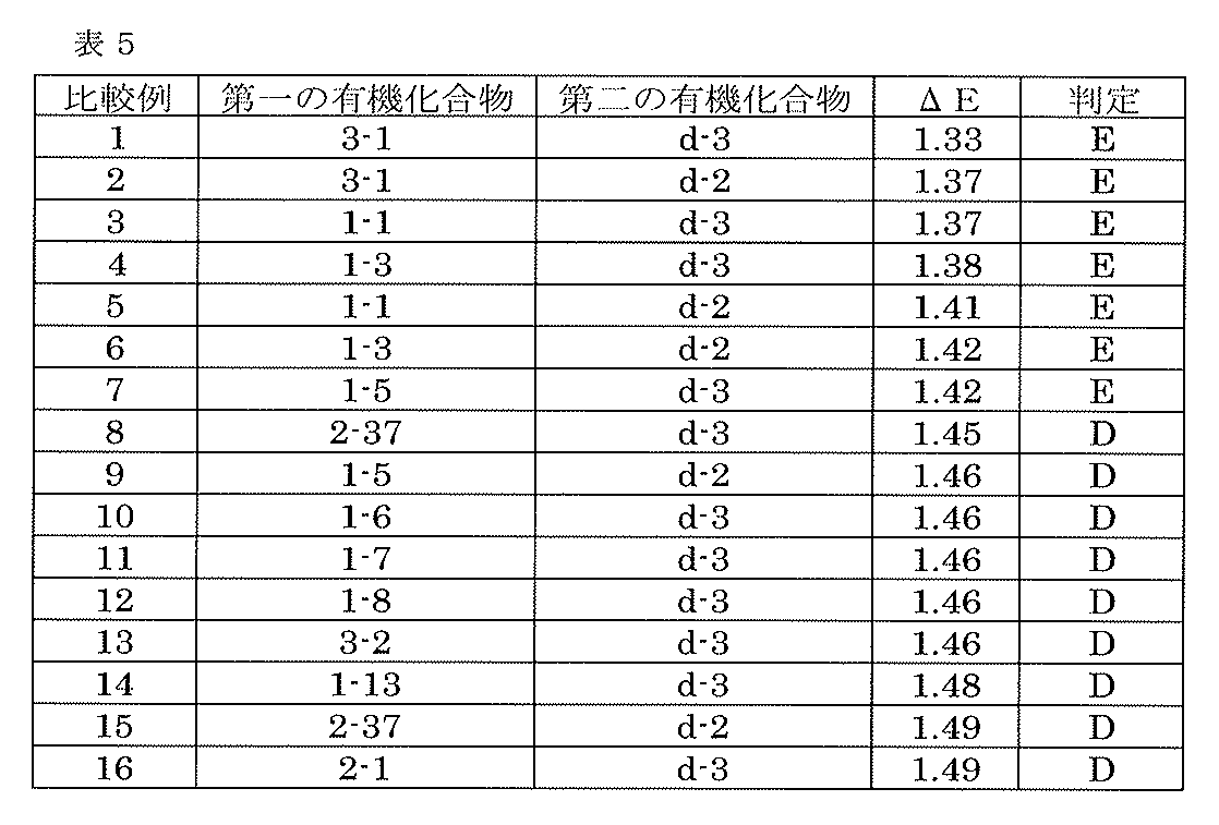
ΔEが1.5V以上の光電変換素子はいずれの組み合わせの素子の暗電流でも評価C以上結果であり低い暗電流特性が得られた。
[実施例48]
実施例2に用いた例示化合物1-7について、混合濃度を20重量%から30重量%まで2.5重量%ずつ変化させた際の暗電流の変化を表6に示す。
実施例2に用いた例示化合物1-7について、混合濃度を20重量%から30重量%まで2.5重量%ずつ変化させた際の暗電流の変化を表6に示す。
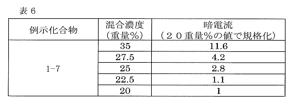
表6より、第一の有機化合物の濃度は、35重量%未満が好ましく、27.5重量%以下であることより好ましい。下限濃度については、本発明において限定されるものではなく、たとえば必要な吸収率が得られる濃度であればよい。
[実施例49-52、比較例17]
構成材料および層厚を表7とした以外は、実施例1と同様にして光電変換素子を作製した。第一の有機化合物は、表8に記載の例示化合物、下記の比較化合物(e-1)を用いた。表7では、第一の有機化合物と記載している。それぞれの素子の暗電流を測定し、相対評価を行った。比較化合物(e-1)の構造は下記の通りである。化合物e-1の酸化電位は0.92Vであった。
構成材料および層厚を表7とした以外は、実施例1と同様にして光電変換素子を作製した。第一の有機化合物は、表8に記載の例示化合物、下記の比較化合物(e-1)を用いた。表7では、第一の有機化合物と記載している。それぞれの素子の暗電流を測定し、相対評価を行った。比較化合物(e-1)の構造は下記の通りである。化合物e-1の酸化電位は0.92Vであった。


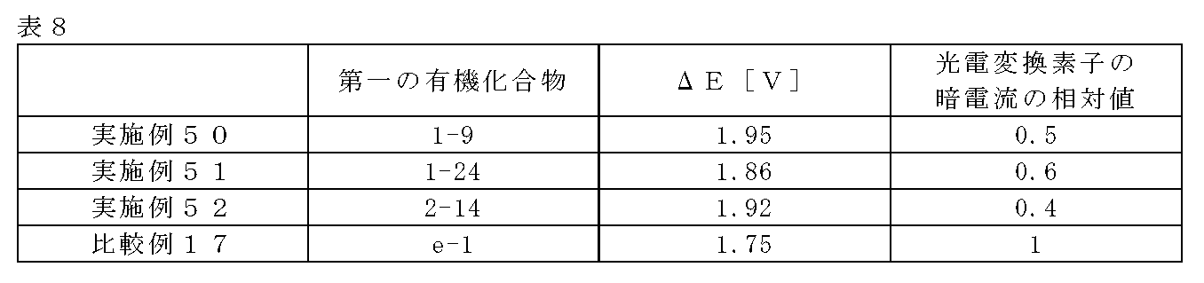
ΔE≧1.5Vとするのみならず、一般式[1]で表される有機化合物を第一の有機化合物として用いることで暗電流を低減することができる。
[実施例53、比較例18]
一般式[28]で記載の部分構造を有する第一の有機化合物について、下記例示化合物の最大吸収ピーク波長とモル吸光係数を示す。最大吸収ピーク波長は、吸収係数が最も大きいピークの波長を指す。測定は、第一の有機化合物がmol/Lのクロロホルム溶液を作製し、分光光度計(日本分光Ubest-550)にて吸収スペクトルを測定した。測定結果より、最大吸収ピーク波長と吸光度を求め。その吸光度からランベールト・ベール則に従ってモル吸光係数を求めた。
一般式[28]で記載の部分構造を有する第一の有機化合物について、下記例示化合物の最大吸収ピーク波長とモル吸光係数を示す。最大吸収ピーク波長は、吸収係数が最も大きいピークの波長を指す。測定は、第一の有機化合物がmol/Lのクロロホルム溶液を作製し、分光光度計(日本分光Ubest-550)にて吸収スペクトルを測定した。測定結果より、最大吸収ピーク波長と吸光度を求め。その吸光度からランベールト・ベール則に従ってモル吸光係数を求めた。

実施例53と比較例18より、一般式[28]で示される化合物は、可視域においてパンクロマティックな吸収帯を得るのに適した吸収ピークと、モル吸光係数40000以上の強い吸収が得られることが分かる。強い吸収は、高い外部量子収率につながるため光電変換素子として重要な因子である。
[実施例54]
封止層にCVD法による窒化珪素層を用いた以外は、実施例1と同様にして光電変換素子を作製した。窒化珪素層は1μmの層厚で形成した。この素子に365nmのLED光を1W/cm2の強度で24h照射して耐久性を評価した。
封止層にCVD法による窒化珪素層を用いた以外は、実施例1と同様にして光電変換素子を作製した。窒化珪素層は1μmの層厚で形成した。この素子に365nmのLED光を1W/cm2の強度で24h照射して耐久性を評価した。
形成したSiN(1μm)の365nmの吸収率は75%であった。この素子は24h後においても、暗電流の値は変化しなかった。
一方、実施例1で作製した光電変換素子は、24時間の光照射後に約10%程度暗電流が上昇した。ガラスキャップは紫外線を吸収率がSiNよりも小さいためである。これを考慮すると、紫外線の吸収可能な材質により封止層を設けることが好ましい。
[実施例55]
実施例1において作製した光電変換素子を用いて、暗電流の温度依存性を測定した。図6は、実施例1の光電変換素子のアレニウスプロットである。縦軸は、60℃における暗電流値で規格化した暗電流値である。縦軸の目盛は常用対数である。横軸は絶対温度の逆数である。60℃付近から高温側に向かって傾きの絶対値が大きくなる。この傾きから次式(5)に従い活性化エネルギーを求めた。
実施例1において作製した光電変換素子を用いて、暗電流の温度依存性を測定した。図6は、実施例1の光電変換素子のアレニウスプロットである。縦軸は、60℃における暗電流値で規格化した暗電流値である。縦軸の目盛は常用対数である。横軸は絶対温度の逆数である。60℃付近から高温側に向かって傾きの絶対値が大きくなる。この傾きから次式(5)に従い活性化エネルギーを求めた。

ここで、T:絶対温度、kB:ボルツマン定数、Ea:活性化エネルギー、J:温度Tでの電流値、J0:頻度因子である。この傾きから暗電流の活性化エネルギーは0.84eVと求めた。
[実施例56]
実施例55の方法と同様にして、実施例2、6、12、34、比較例6において作製した光電変換素子について活性化エネルギーを求めて、対応するΔEに対してプロットしたのが図7である。ΔEが大きいほど、活性化エネルギーが大きくなる傾向がわかる。図7より、ΔEが1.5V以上となることで、活性化エネルギーが大きいことがわかる。これは、ΔEが1.5V以上である場合、熱励起による電荷発生確率が低下することを指す。ここで、活性化エネルギーと暗電流の評価との関係を表10に示す。表に示す通り、活性化エネルギーが、0.70eV以上の場合、暗電流の評価がC以上となる。
実施例55の方法と同様にして、実施例2、6、12、34、比較例6において作製した光電変換素子について活性化エネルギーを求めて、対応するΔEに対してプロットしたのが図7である。ΔEが大きいほど、活性化エネルギーが大きくなる傾向がわかる。図7より、ΔEが1.5V以上となることで、活性化エネルギーが大きいことがわかる。これは、ΔEが1.5V以上である場合、熱励起による電荷発生確率が低下することを指す。ここで、活性化エネルギーと暗電流の評価との関係を表10に示す。表に示す通り、活性化エネルギーが、0.70eV以上の場合、暗電流の評価がC以上となる。
すなわち、暗電流の活性化エネルギーが0.70eV以上であることが暗電流を低減するために好ましい。

以上のことから本発明に係る光電変換素子は、暗電流が低減された光電変換素子である。これを有する撮像素子は、光電変換素子部に由来する暗電流ノイズが少ないので好ましい。
本発明は上記実施の形態に制限されるものではなく、本発明の精神及び範囲から離脱することなく、様々な変更及び変形が可能である。従って、本発明の範囲を公にするために以下の請求項を添付する。
本願は、2016年11月11日提出の日本国特許出願特願2016-220717と2017年9月15日提出の日本国特許出願特願2017-177880を基礎として優先権を主張するものであり、その記載内容の全てをここに援用する。
Claims (16)
- アノードと、カソードと、前記アノードと前記カソードとの間に配置されている光電変換層と、を有する光電変換素子であって、
前記光電変換層は第一の有機化合物と第二の有機化合物とを有し、前記第一の有機化合物の酸化電位は、前記第二の有機化合物の酸化電位よりも小さく、下記式(A)であらわされるΔEが、下記式(B)を満たし、
ΔE=第一の有機化合物の酸化電位-第二の有機化合物の還元電位 (A)
ΔE≧1.5 [V] (B)
前記第一の有機化合物が下記一般式[1]乃至[5]のいずれかであることを特徴とする光電変換素子。

一般式[1]において、R1は水素原子、ハロゲン原子、置換あるいは無置換のアルキル基、置換あるいは無置換のアルコキシ基、置換あるいは無置換のアリール基、置換あるいは無置換の複素環基、置換あるいは無置換のビニル基、置換あるいは無置換のアミノ基、シアノ基を表す。
n1及びn2は0乃至4までの整数を表す。X1乃至X3は窒素原子、硫黄原子、酸素原子または炭素原子を表わし、当該炭素原子は、置換基を有してもよい。
Ar1及びAr2は置換あるいは無置換のアリール基、または置換あるいは無置換の複素環基からそれぞれ独立に選ばれる。
Ar1及びAr2が複数ある場合はそれぞれ同じでも異なってもよく、Ar1及びAr2はX2あるいはX3が炭素原子の場合、互いに結合して環を形成してもよい。
Z1はハロゲン原子、シアノ基、置換あるいは無置換のヘテロアリール基または以下の一般式[1-1]乃至[1-9]で表される置換基のいずれかを表す。
一般式[1-1]乃至[1-9]において、R521乃至R588は水素原子、ハロゲン原子、置換あるいは無置換のアルキル基、置換あるいは無置換のアルコキシ基、置換あるいは無置換のアリール基、置換あるいは無置換の複素環基、置換あるいは無置換のビニル基、置換あるいは無置換のアミノ基、シアノ基からそれぞれ独立に選ばれる。

一般式[2]においてR20乃至R29は水素原子、ハロゲン原子、置換あるいは無置換のアルキル基、置換あるいは無置換のアルコキシ基、置換あるいは無置換のアリール基、置換あるいは無置換の複素環基、置換あるいは無置換のビニル基、置換あるいは無置換のアミノ基、シアノ基からそれぞれ独立に選ばれる。R20乃至R29のうちの隣り合う2つは互いに結合して環を形成してもよい。
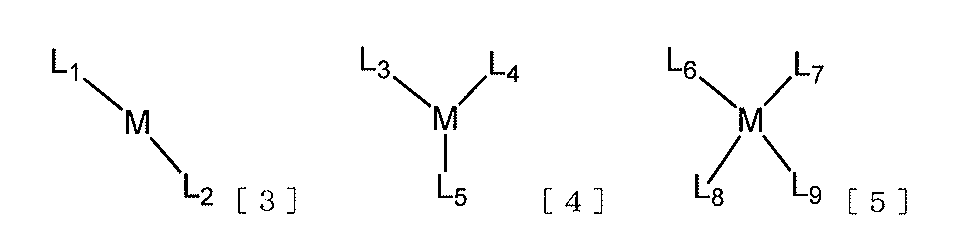
一般式[3]乃至[5]において、Mは金属原子を表す。当該金属原子は酸素原子またはハロゲン原子を置換基として有してもよい。
L1乃至L9は金属Mに配位する配位子を表す。当該配位子は、置換あるいは無置換のアリール基、置換あるいは無置換の複素環基からなり、それぞれL1乃至L9のうちの隣り合う2つは互いに結合して環を形成してもよい。 - 前記一般式[1]において、Ar1が前記アリール基または前記複素環基であり、X1が硫黄原子または酸素原子であり、n1が1であり、n2が0であることを特徴とする請求項1に記載の光電変換素子。
- 前記一般式[2]が以下に示す一般式[11]乃至[27]であることを特徴とする請求項1または2に記載の光電変換素子。


式[11]乃至[27]において、R31乃至R390は、水素原子、ハロゲン原子、置換あるいは無置換のアルキル基、置換あるいは無置換のアルコキシ基、置換あるいは無置換のアリール基、置換あるいは無置換の複素環基、置換あるいは無置換のビニル基、置換あるいは無置換のアミノ基、シアノ基からそれぞれ独立に選ばれる。 - 前記一般式[3]乃至[5]において、Mがイリジウム、プラチナ、バナジウム、コバルト、ガリウム、チタンのいずれかであることを特徴とする請求項1乃至3のいずれか一項に記載の光電変換素子。
- アノードと、カソードと、前記アノードと前記カソードとの間に配置されている光電変換層と、を有する光電変換素子であって、
暗電流の活性化エネルギーが、0.70eV以上であることを特徴とする光電変換素子。 - 前記光電変換層は、第一の有機化合物と、第二の有機化合物とを有し、
前記第一の有機化合物の酸化電位は、前記第二の有機化合物の酸化電位よりも小さいことを特徴とする請求項5に記載の光電変換素子。 - 前記第一の有機化合物の吸収ピーク波長は、530nm以上であることを特徴とする請求項1乃至6のいずれか一項に記載の光電変換素子。
- 前記第一の有機化合物の酸化電位が、0.65V以上であることを特徴とする請求項1乃至7のいずれか一項に記載の光電変換素子。
- 前記第二の有機化合物がフラーレン誘導体であることを特徴とする請求項1乃至8のいずれか一項に記載の光電変換素子。
- 前記フラーレン誘導体が、フラーレンC60であることを特徴とする請求項9に記載の光電変換素子。
- 前記上部電極の上に封止層を有することを特徴とする請求項1乃至10のいずれか一項に記載の光電変換素子。
- 複数の画素と、前記画素に接続されている信号処理回路と、を有する撮像素子であって、
前記画素は、請求項1乃至11のいずれか一項に記載の光電変換素子と、前記光電変換素子に接続されている読み出し回路とを有することを特徴とする撮像素子。 - 複数のレンズを有する光学部と、前記光学部を透過した光を受光する撮像素子とを有し、
前記撮像素子は、請求項12に記載の撮像素子であることを特徴とする撮像装置。 - 外部からの信号を受信する受信部をさらに有することを特徴とする請求項13に記載の撮像装置。
- 前記信号は、前記撮像装置の撮像範囲、撮像の開始、撮像の終了の少なくともいずれかを制御する信号であることを特徴とする請求項14に記載の撮像装置。
- 取得した画像を外部に送信する送信部をさらに有することを特徴とする請求項13乃至15のいずれか一項に記載の撮像装置。
Priority Applications (3)
| Application Number | Priority Date | Filing Date | Title |
|---|---|---|---|
| EP17870234.6A EP3540804A4 (en) | 2016-11-11 | 2017-11-02 | PHOTOELECTRIC CONVERSION ELEMENT, IMAGING ELEMENT, AND IMAGING DEVICE |
| CN201780069863.6A CN109937489B (zh) | 2016-11-11 | 2017-11-02 | 光电转换元件、摄像元件和摄像设备 |
| US16/407,012 US20190267411A1 (en) | 2016-11-11 | 2019-05-08 | Photoelectric conversion element, image pickup element, and image pickup apparatus |
Applications Claiming Priority (4)
| Application Number | Priority Date | Filing Date | Title |
|---|---|---|---|
| JP2016220717 | 2016-11-11 | ||
| JP2016-220717 | 2016-11-11 | ||
| JP2017-177880 | 2017-09-15 | ||
| JP2017177880A JP7102114B2 (ja) | 2016-11-11 | 2017-09-15 | 光電変換素子、撮像素子および撮像装置 |
Related Child Applications (1)
| Application Number | Title | Priority Date | Filing Date |
|---|---|---|---|
| US16/407,012 Continuation US20190267411A1 (en) | 2016-11-11 | 2019-05-08 | Photoelectric conversion element, image pickup element, and image pickup apparatus |
Publications (1)
| Publication Number | Publication Date |
|---|---|
| WO2018088325A1 true WO2018088325A1 (ja) | 2018-05-17 |
Family
ID=62109779
Family Applications (1)
| Application Number | Title | Priority Date | Filing Date |
|---|---|---|---|
| PCT/JP2017/039722 WO2018088325A1 (ja) | 2016-11-11 | 2017-11-02 | 光電変換素子、撮像素子および撮像装置 |
Country Status (1)
| Country | Link |
|---|---|
| WO (1) | WO2018088325A1 (ja) |
Citations (10)
| Publication number | Priority date | Publication date | Assignee | Title |
|---|---|---|---|---|
| JP2001064640A (ja) * | 1999-08-30 | 2001-03-13 | Toyo Ink Mfg Co Ltd | 有機エレクトロルミネッセンス素子用材料およびそれを使用した有機エレクトロルミネッセンス素子 |
| US20050110007A1 (en) * | 2003-11-26 | 2005-05-26 | Forrest Stephen R. | Multilayer organic photodetectors with improved performance |
| JP2010147158A (ja) * | 2008-12-17 | 2010-07-01 | Mitsubishi Electric Corp | 半導体受光素子および半導体受光素子の製造方法 |
| JP2010183060A (ja) * | 2008-10-15 | 2010-08-19 | Fujifilm Corp | 光電変換素子及び撮像素子 |
| JP2010219212A (ja) * | 2009-03-16 | 2010-09-30 | Konica Minolta Holdings Inc | 有機エレクトロニクス素子、有機光電変換素子、及び有機エレクトロルミネッセンス素子 |
| JP2011077198A (ja) * | 2009-09-29 | 2011-04-14 | Fujifilm Corp | 光電変換素子、光電変換素子材料、光センサ、及び撮像素子 |
| JP2012188355A (ja) * | 2011-03-08 | 2012-10-04 | Canon Inc | 新規有機化合物およびそれを有する有機発光素子 |
| FR3011548A1 (fr) * | 2013-10-07 | 2015-04-10 | Arkema France | Compose organique photoactif |
| JP2017143133A (ja) * | 2016-02-09 | 2017-08-17 | キヤノン株式会社 | 有機光電変換素子、光エリアセンサ、撮像素子及び撮像装置 |
| JP2017214353A (ja) * | 2016-05-31 | 2017-12-07 | キヤノン株式会社 | 光電変換素子、二次元センサ、画像センサおよび撮像装置 |
-
2017
- 2017-11-02 WO PCT/JP2017/039722 patent/WO2018088325A1/ja unknown
Patent Citations (10)
| Publication number | Priority date | Publication date | Assignee | Title |
|---|---|---|---|---|
| JP2001064640A (ja) * | 1999-08-30 | 2001-03-13 | Toyo Ink Mfg Co Ltd | 有機エレクトロルミネッセンス素子用材料およびそれを使用した有機エレクトロルミネッセンス素子 |
| US20050110007A1 (en) * | 2003-11-26 | 2005-05-26 | Forrest Stephen R. | Multilayer organic photodetectors with improved performance |
| JP2010183060A (ja) * | 2008-10-15 | 2010-08-19 | Fujifilm Corp | 光電変換素子及び撮像素子 |
| JP2010147158A (ja) * | 2008-12-17 | 2010-07-01 | Mitsubishi Electric Corp | 半導体受光素子および半導体受光素子の製造方法 |
| JP2010219212A (ja) * | 2009-03-16 | 2010-09-30 | Konica Minolta Holdings Inc | 有機エレクトロニクス素子、有機光電変換素子、及び有機エレクトロルミネッセンス素子 |
| JP2011077198A (ja) * | 2009-09-29 | 2011-04-14 | Fujifilm Corp | 光電変換素子、光電変換素子材料、光センサ、及び撮像素子 |
| JP2012188355A (ja) * | 2011-03-08 | 2012-10-04 | Canon Inc | 新規有機化合物およびそれを有する有機発光素子 |
| FR3011548A1 (fr) * | 2013-10-07 | 2015-04-10 | Arkema France | Compose organique photoactif |
| JP2017143133A (ja) * | 2016-02-09 | 2017-08-17 | キヤノン株式会社 | 有機光電変換素子、光エリアセンサ、撮像素子及び撮像装置 |
| JP2017214353A (ja) * | 2016-05-31 | 2017-12-07 | キヤノン株式会社 | 光電変換素子、二次元センサ、画像センサおよび撮像装置 |
Similar Documents
| Publication | Publication Date | Title |
|---|---|---|
| JP7102114B2 (ja) | 光電変換素子、撮像素子および撮像装置 | |
| US11128791B2 (en) | Photoelectric conversion element | |
| WO2018088313A1 (ja) | 光電変換素子、それを有する撮像素子及び撮像装置 | |
| JP6645700B2 (ja) | 有機光電変換素子、二次元センサ、画像センサ及び撮像装置 | |
| WO2017138363A1 (ja) | 有機光電変換素子、光エリアセンサ、撮像素子及び撮像装置 | |
| JP6833351B2 (ja) | 有機光電変換素子、光エリアセンサ、撮像素子および撮像装置 | |
| JP2022021347A (ja) | 有機化合物及び有機光電変換素子 | |
| JP7013163B2 (ja) | 有機化合物及び光電変換素子 | |
| JP6932564B2 (ja) | 有機光電変換素子、撮像素子及び撮像装置 | |
| WO2018147202A1 (ja) | 光電変換素子、及びこれを用いた光エリアセンサ、撮像素子、撮像装置 | |
| JP2019055919A (ja) | 有機化合物及び光電変換素子 | |
| US11895910B2 (en) | Organic compound and photoelectric conversion element | |
| WO2018088325A1 (ja) | 光電変換素子、撮像素子および撮像装置 | |
| JP7086573B2 (ja) | 光電変換素子、及びこれを用いた光エリアセンサ、撮像素子、撮像装置 | |
| JP7016662B2 (ja) | 有機化合物、それを用いた光電変換素子および撮像装置 | |
| JP2017137264A (ja) | 有機化合物、赤外光吸収材料及びその利用 | |
| JP2018078240A (ja) | 光電変換素子、それを有する撮像素子及び撮像装置 | |
| JP7039285B2 (ja) | 光電変換素子、及びこれを用いた光エリアセンサ、撮像素子、撮像装置 | |
| US10468614B2 (en) | Photoelectric conversion element, image pick-up element, and image pick-up apparatus | |
| JP7367050B2 (ja) | 光電変換素子、撮像素子、光センサ、光電変換素子用材料、化合物 | |
| JP2017174921A (ja) | 有機光電変換素子、二次元センサ、画像センサ及び撮像装置 | |
| CN115700059A (zh) | 光电转换元件、摄像元件、光传感器及化合物 |
Legal Events
| Date | Code | Title | Description |
|---|---|---|---|
| 121 | Ep: the epo has been informed by wipo that ep was designated in this application |
Ref document number: 17870234 Country of ref document: EP Kind code of ref document: A1 |
|
| NENP | Non-entry into the national phase |
Ref country code: DE |
|
| ENP | Entry into the national phase |
Ref document number: 2017870234 Country of ref document: EP Effective date: 20190611 |