WO2018087943A1 - Mosfet及び電力変換回路 - Google Patents
Mosfet及び電力変換回路 Download PDFInfo
- Publication number
- WO2018087943A1 WO2018087943A1 PCT/JP2017/011066 JP2017011066W WO2018087943A1 WO 2018087943 A1 WO2018087943 A1 WO 2018087943A1 JP 2017011066 W JP2017011066 W JP 2017011066W WO 2018087943 A1 WO2018087943 A1 WO 2018087943A1
- Authority
- WO
- WIPO (PCT)
- Prior art keywords
- mosfet
- type column
- column region
- depth position
- region
- Prior art date
- Legal status (The legal status is an assumption and is not a legal conclusion. Google has not performed a legal analysis and makes no representation as to the accuracy of the status listed.)
- Ceased
Links
Images








Classifications
-
- H—ELECTRICITY
- H10—SEMICONDUCTOR DEVICES; ELECTRIC SOLID-STATE DEVICES NOT OTHERWISE PROVIDED FOR
- H10D—INORGANIC ELECTRIC SEMICONDUCTOR DEVICES
- H10D30/00—Field-effect transistors [FET]
- H10D30/60—Insulated-gate field-effect transistors [IGFET]
- H10D30/64—Double-diffused metal-oxide semiconductor [DMOS] FETs
- H10D30/66—Vertical DMOS [VDMOS] FETs
- H10D30/668—Vertical DMOS [VDMOS] FETs having trench gate electrodes, e.g. UMOS transistors
-
- H—ELECTRICITY
- H02—GENERATION; CONVERSION OR DISTRIBUTION OF ELECTRIC POWER
- H02M—APPARATUS FOR CONVERSION BETWEEN AC AND AC, BETWEEN AC AND DC, OR BETWEEN DC AND DC, AND FOR USE WITH MAINS OR SIMILAR POWER SUPPLY SYSTEMS; CONVERSION OF DC OR AC INPUT POWER INTO SURGE OUTPUT POWER; CONTROL OR REGULATION THEREOF
- H02M3/00—Conversion of DC power input into DC power output
- H02M3/02—Conversion of DC power input into DC power output without intermediate conversion into AC
- H02M3/04—Conversion of DC power input into DC power output without intermediate conversion into AC by static converters
- H02M3/10—Conversion of DC power input into DC power output without intermediate conversion into AC by static converters using discharge tubes with control electrode or semiconductor devices with control electrode
- H02M3/145—Conversion of DC power input into DC power output without intermediate conversion into AC by static converters using discharge tubes with control electrode or semiconductor devices with control electrode using devices of a triode or transistor type requiring continuous application of a control signal
- H02M3/155—Conversion of DC power input into DC power output without intermediate conversion into AC by static converters using discharge tubes with control electrode or semiconductor devices with control electrode using devices of a triode or transistor type requiring continuous application of a control signal using semiconductor devices only
-
- H—ELECTRICITY
- H10—SEMICONDUCTOR DEVICES; ELECTRIC SOLID-STATE DEVICES NOT OTHERWISE PROVIDED FOR
- H10D—INORGANIC ELECTRIC SEMICONDUCTOR DEVICES
- H10D30/00—Field-effect transistors [FET]
-
- H—ELECTRICITY
- H10—SEMICONDUCTOR DEVICES; ELECTRIC SOLID-STATE DEVICES NOT OTHERWISE PROVIDED FOR
- H10D—INORGANIC ELECTRIC SEMICONDUCTOR DEVICES
- H10D30/00—Field-effect transistors [FET]
- H10D30/60—Insulated-gate field-effect transistors [IGFET]
- H10D30/64—Double-diffused metal-oxide semiconductor [DMOS] FETs
- H10D30/66—Vertical DMOS [VDMOS] FETs
-
- H—ELECTRICITY
- H10—SEMICONDUCTOR DEVICES; ELECTRIC SOLID-STATE DEVICES NOT OTHERWISE PROVIDED FOR
- H10D—INORGANIC ELECTRIC SEMICONDUCTOR DEVICES
- H10D30/00—Field-effect transistors [FET]
- H10D30/60—Insulated-gate field-effect transistors [IGFET]
- H10D30/64—Double-diffused metal-oxide semiconductor [DMOS] FETs
- H10D30/66—Vertical DMOS [VDMOS] FETs
- H10D30/667—Vertical DMOS [VDMOS] FETs having substrates comprising insulating layers, e.g. SOI-VDMOS transistors
-
- H—ELECTRICITY
- H10—SEMICONDUCTOR DEVICES; ELECTRIC SOLID-STATE DEVICES NOT OTHERWISE PROVIDED FOR
- H10D—INORGANIC ELECTRIC SEMICONDUCTOR DEVICES
- H10D62/00—Semiconductor bodies, or regions thereof, of devices having potential barriers
- H10D62/10—Shapes, relative sizes or dispositions of the regions of the semiconductor bodies; Shapes of the semiconductor bodies
- H10D62/102—Constructional design considerations for preventing surface leakage or controlling electric field concentration
- H10D62/103—Constructional design considerations for preventing surface leakage or controlling electric field concentration for increasing or controlling the breakdown voltage of reverse-biased devices
- H10D62/105—Constructional design considerations for preventing surface leakage or controlling electric field concentration for increasing or controlling the breakdown voltage of reverse-biased devices by having particular doping profiles, shapes or arrangements of PN junctions; by having supplementary regions, e.g. junction termination extension [JTE]
- H10D62/109—Reduced surface field [RESURF] PN junction structures
- H10D62/111—Multiple RESURF structures, e.g. double RESURF or 3D-RESURF structures
-
- H—ELECTRICITY
- H10—SEMICONDUCTOR DEVICES; ELECTRIC SOLID-STATE DEVICES NOT OTHERWISE PROVIDED FOR
- H10D—INORGANIC ELECTRIC SEMICONDUCTOR DEVICES
- H10D62/00—Semiconductor bodies, or regions thereof, of devices having potential barriers
- H10D62/10—Shapes, relative sizes or dispositions of the regions of the semiconductor bodies; Shapes of the semiconductor bodies
- H10D62/13—Semiconductor regions connected to electrodes carrying current to be rectified, amplified or switched, e.g. source or drain regions
- H10D62/149—Source or drain regions of field-effect devices
- H10D62/151—Source or drain regions of field-effect devices of IGFETs
- H10D62/152—Source regions of DMOS transistors
-
- H—ELECTRICITY
- H10—SEMICONDUCTOR DEVICES; ELECTRIC SOLID-STATE DEVICES NOT OTHERWISE PROVIDED FOR
- H10D—INORGANIC ELECTRIC SEMICONDUCTOR DEVICES
- H10D62/00—Semiconductor bodies, or regions thereof, of devices having potential barriers
- H10D62/10—Shapes, relative sizes or dispositions of the regions of the semiconductor bodies; Shapes of the semiconductor bodies
- H10D62/13—Semiconductor regions connected to electrodes carrying current to be rectified, amplified or switched, e.g. source or drain regions
- H10D62/149—Source or drain regions of field-effect devices
- H10D62/151—Source or drain regions of field-effect devices of IGFETs
- H10D62/156—Drain regions of DMOS transistors
-
- H—ELECTRICITY
- H10—SEMICONDUCTOR DEVICES; ELECTRIC SOLID-STATE DEVICES NOT OTHERWISE PROVIDED FOR
- H10D—INORGANIC ELECTRIC SEMICONDUCTOR DEVICES
- H10D62/00—Semiconductor bodies, or regions thereof, of devices having potential barriers
- H10D62/10—Shapes, relative sizes or dispositions of the regions of the semiconductor bodies; Shapes of the semiconductor bodies
- H10D62/13—Semiconductor regions connected to electrodes carrying current to be rectified, amplified or switched, e.g. source or drain regions
- H10D62/149—Source or drain regions of field-effect devices
- H10D62/151—Source or drain regions of field-effect devices of IGFETs
- H10D62/156—Drain regions of DMOS transistors
- H10D62/157—Impurity concentrations or distributions
-
- H—ELECTRICITY
- H10—SEMICONDUCTOR DEVICES; ELECTRIC SOLID-STATE DEVICES NOT OTHERWISE PROVIDED FOR
- H10D—INORGANIC ELECTRIC SEMICONDUCTOR DEVICES
- H10D62/00—Semiconductor bodies, or regions thereof, of devices having potential barriers
- H10D62/10—Shapes, relative sizes or dispositions of the regions of the semiconductor bodies; Shapes of the semiconductor bodies
- H10D62/13—Semiconductor regions connected to electrodes carrying current to be rectified, amplified or switched, e.g. source or drain regions
- H10D62/149—Source or drain regions of field-effect devices
- H10D62/151—Source or drain regions of field-effect devices of IGFETs
- H10D62/156—Drain regions of DMOS transistors
- H10D62/159—Shapes
-
- H—ELECTRICITY
- H10—SEMICONDUCTOR DEVICES; ELECTRIC SOLID-STATE DEVICES NOT OTHERWISE PROVIDED FOR
- H10D—INORGANIC ELECTRIC SEMICONDUCTOR DEVICES
- H10D62/00—Semiconductor bodies, or regions thereof, of devices having potential barriers
- H10D62/80—Semiconductor bodies, or regions thereof, of devices having potential barriers characterised by the materials
- H10D62/83—Semiconductor bodies, or regions thereof, of devices having potential barriers characterised by the materials being Group IV materials, e.g. B-doped Si or undoped Ge
- H10D62/832—Semiconductor bodies, or regions thereof, of devices having potential barriers characterised by the materials being Group IV materials, e.g. B-doped Si or undoped Ge being Group IV materials comprising two or more elements, e.g. SiGe
- H10D62/8325—Silicon carbide
-
- H—ELECTRICITY
- H10—SEMICONDUCTOR DEVICES; ELECTRIC SOLID-STATE DEVICES NOT OTHERWISE PROVIDED FOR
- H10D—INORGANIC ELECTRIC SEMICONDUCTOR DEVICES
- H10D8/00—Diodes
- H10D8/60—Schottky-barrier diodes
Definitions
- the present invention relates to a MOSFET and a power conversion circuit.
- MOSFET including a semiconductor substrate having a super junction structure composed of an n-type column region and a p-type column region is known (see, for example, Patent Document 1).
- the super junction structure refers to a structure in which n-type column regions and p-type column regions are alternately arranged when viewed in a predetermined cross section.
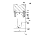
- a conventional MOSFET 900 includes a super junction structure 917 composed of an n-type column region 914 and a p-type column region 916, a surface of a first main surface, and a surface of the p-type column region 916. And a base region 918 formed on a part of the surface of the n-type column region 914 and a surface of the first main surface and on the surface of the n-type column region 914 so as to be adjacent to the base region 918.
- N-type surface high-concentration region 919 and n-type source region 920 formed on the surface of base region 918, and sandwiched between source region 920 and n-type surface high-concentration region 919
- This is a planar gate type MOSFET including a gate electrode 936 formed on the surface of the base region 918 via a gate insulating film 934.
- the n-type column region 914 and the p-type column region 916 are formed so that the total amount of impurities in the n-type column region 914 is equal to the total amount of impurities in the p-type column region 916. That is, the n-type column region 914 and the p-type column region 916 are in charge balance. Further, the impurity concentration of the n-type column region 914 and the impurity concentration of the p-type column region 916 are both constant regardless of the depth. Furthermore, the sidewall of the n-type column region 914 has a tapered shape with a narrow first main surface, and the sidewall of the p-type column region 916 has a tapered shape with a narrow bottom.
- total amount of impurities refers to the total amount of impurities in the components (n-type column region or p-type column region) in the MOSFET.
- the conventional MOSFET 900 includes the semiconductor substrate 910 having the super junction structure 917 composed of the n-type column region 914 and the p-type column region 916, it becomes a low on-resistance and high breakdown voltage switching element.
- the conventional MOSFET 900 has a problem that if the charge balance around the gate varies, the variation in switching characteristics when turned off increases.
- the present invention has been made to solve the above-described problems, and even if there is a variation in charge balance around the gate, a MOSFET capable of reducing variation in switching characteristics when turned off as compared with the conventional MOSFET, and this An object of the present invention is to provide a power conversion circuit using the.
- a MOSFET of the present invention is formed on a semiconductor substrate having a super junction structure composed of an n-type column region and a p-type column region, and on the first main surface side of the semiconductor substrate via a gate insulating film.
- the horizontal axis is a depth x at a predetermined depth position in the super junction structure, and the MOSFET is turned off and the super junction structure is depleted.
- the average positive charge density ⁇ (x) at the predetermined depth position is the vertical axis
- the average positive charge density ⁇ (x) is represented by an upwardly convex curve
- the MOSFET is turned off with reference to the deepest depth position of the surface of the depletion layer on the first main surface side when the depletion layer spreads most in the super junction structure after being turned off, and the super junction structure is depleted.
- the average positive charge density ⁇ (0) of x 0
- w n (x) represents the width of the n-type column region at the predetermined depth position
- N d (x) represents depletion of the super junction structure by turning off the MOSFET.
- the average density of positive charges at the predetermined depth position of the n-type column region is shown
- w p (x) indicates the width of the p-type column region at the predetermined depth position
- N a ( x) represents an average density of negative charges at the predetermined depth position of the p-type column region when the MOSFET is turned off and the super junction structure is depleted
- q represents an elementary electric quantity
- the depth at a predetermined depth position in the super junction structure means the surface of the depletion layer on the first main surface side when the MOSFET is turned off and the depletion layer spreads most in the super junction structure.
- the depth of a predetermined depth position in the super junction structure based on the deepest depth position. Therefore, the depth x is 0 at the deepest depth position in the surface of the depletion layer on the first main surface side when the MOSFET is turned off and the depletion layer spreads most in the super junction structure.
- the “second main surface” refers to a main surface opposite to the first main surface.
- the “average density of positive charges in the n-type column region” is an average density of positive charges caused by donors in the n-type column region when the MOSFET is turned off and the n-type column region is depleted.
- Average density of negative charges in the p-type column region is an average density of negative charges caused by acceptors in the p-type column region when the MOSFET is turned off and the p-type column region is depleted. Show.
- the average positive charge density ⁇ (x) at a predetermined depth position of the super junction structure is represented by an upward convex curve” means that the average positive charge density is a monotonous convex upward.
- the average positive charge density is a stepped shape (however, the line connecting the corners of the steps (envelope) is a monotonous curve rising upward) And the case where the average positive charge density is expressed by a curved line in which irregularities are repeated (however, the envelope becomes a monotonically rising curve that is convex upward).
- the deepest depth position of the surface of the depletion layer on the first main surface side when the MOSFET is turned off and the depletion layer spreads most in the super junction structure is used as a reference.
- the depth of the shallowest depth position of the surface of the depletion layer on the second main surface side when the depletion layer spreads most in the super junction structure by turning off the MOSFET is defined as a, and in the super junction structure It is preferable that 0 ⁇ d ⁇ a / 2 is satisfied, where d is the depth at which the average positive charge density ⁇ (x) becomes 0.
- the horizontal axis is the depth x of the predetermined depth position in the super junction structure, and the width w n (x) of the n-type column region at the predetermined depth position or the p
- the width w n (x) at the predetermined depth position of the type column region is the vertical axis
- the width w n (x) at the predetermined depth position of the n-type column region is raised upward to the right
- the width w p (x) at the predetermined depth position of the p-type column region is represented by a downwardly convex right-down curve.
- the average density N d (x) of positive charges at the predetermined depth position or the average density N a (x) of negative charges at the predetermined depth position of the p-type column region is the vertical axis.
- the average density N d (x) of positive charges at the predetermined depth position of the n-type column region when the super junction structure is depleted by turning off is expressed by an upward convex curve
- the p-type column region is at the predetermined depth position.
- Takes the average density N a negative charge (x) is preferably represented by the convex curve downward-sloping down.
- the semiconductor substrate includes a p-type base region formed on the surfaces of the n-type column region and the p-type column region, and an n-type formed on the surface of the base region.
- the MOSFET further includes a source region of a type, and the MOSFET is located in a region where the n-type column region is located in plan view from a surface of the first main surface of the semiconductor substrate to a deepest portion of the base region. It further comprises a trench formed so that a part of the source region is exposed to the inner peripheral surface up to a deep depth position, and the gate insulating film is formed on the inner peripheral surface of the trench,
- the gate electrode is preferably embedded in the trench via the gate insulating film.
- the semiconductor substrate is a surface of the first main surface of the semiconductor substrate, a whole surface of the p-type column region, and a surface of the n-type column region.
- a base region formed in a portion, a surface of the first main surface of the semiconductor substrate, and an n-type surface high concentration region formed on the surface of the n-type column region so as to be adjacent to the base region;
- An n-type source region formed on the surface of the base region, and the gate electrode is formed on the surface of the base region sandwiched between the source region and the n-type surface high concentration region. It is preferably formed through a gate insulating film.
- the deepest depth position of the surface of the depletion layer on the first main surface side when the MOSFET is turned off and the depletion layer spreads most in the super junction structure is used as a reference.
- the axis along the depth direction is the x axis
- the x coordinate of the depth position of the lowermost surface of the base region is -t
- the x coordinate of the depth position of the lowermost portion of the p-type column region is b
- the power conversion circuit according to any one of [1] to [7], wherein the power conversion circuit according to the present invention controls a reactor, a power source that supplies current to the reactor, and a current that is supplied from the power source to the reactor. It comprises at least a MOSFET and a rectifying element that performs a rectifying operation of a current supplied from the power source to the reactor or a current from the reactor.
- the rectifying element is preferably a fast recovery diode.
- the rectifying element is preferably a built-in diode of the MOSFET.
- the rectifying element is preferably a silicon carbide Schottky barrier diode.
- the average positive charge density ⁇ (x) at a predetermined depth position of the super junction structure is convex upward. Since it is represented by a curve rising to the right, the average positive charge density ⁇ (x) is smaller (larger on the negative side) than the conventional MOSFET 900 at the depth position around the gate (region where x is close to 0). The difference between the negative charge amount of the p-type column region and the positive charge amount of the n-type column region is larger than that of the conventional MOSFET 900.
- the n-type column region around the gate is more easily depleted than the conventional MOSFET 900, the potential of the n-type column region around the gate is hardly increased even if the drain voltage is increased.
- the distance between the non-depleted region in the n-type column region and the gate electrode is longer than that of the conventional MOSFET 900, and the feedback capacitance Crss (equal to the gate-drain capacitance Cgd) is higher than that of the conventional MOSFET 900.
- the gate electrode becomes n It becomes difficult to be affected by the potential change in the mold column region. As a result, even if there is a variation in charge balance around the gate, the variation in switching characteristics when turned off can be made smaller than before.
- the average positive charge density ⁇ (x) at a predetermined depth position of the superjunction structure rises upward to the right Therefore, in the depth position around the gate, the average positive charge density ⁇ (x) is small (large on the negative side), and the negative charge amount in the p-type column region is n-type column region. It becomes larger than the positive charge amount. Therefore, it becomes easy to draw holes around the gate of the p-type column region due to the negative charge of the p-type column region, and as a result, the L load avalanche breakdown resistance can be made larger than before.
- the semiconductor substrate having a super junction structure composed of the n-type column region and the p-type column region is provided, as in the case of the conventional MOSFET 900, low on-resistance and high It becomes a withstand voltage switching element.
- Patent Document 2 describes a MOSFET 902 in which the width of the p-type column region 816 extends from the center in the depth direction to the bottom of the p-type column region 816 (see FIG. 18).
- the MOSFET 902 according to Patent Document 2 has an average positive charge density ⁇ ( This is different from the MOSFET of the present invention in which x) is represented by an upward convex curve.
- FIG. 1 is a circuit diagram showing a power conversion circuit 1 according to Embodiment 1.
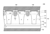
- FIG. 1 is a cross-sectional view showing a MOSFET 100 according to Embodiment 1.
- FIG. It is a schematic diagram shown in order to demonstrate average positive charge density (rho) (x) in the predetermined depth position of a super junction structure when MOSFET is turned off and a super junction structure is depleted.
- rho average positive charge density
- the left x-axis indicates the depth with reference to the deepest depth position of the surface of the depletion layer on the first main surface side when the MOSFET is turned off and the depletion layer spreads most in the super junction structure.
- a position along the direction where the x coordinate is -t is the depth position of the bottom surface of the base region 118, and a position where the x coordinate is b is the depth position of the bottom portion of the p-type column region 116.
- the position where the x coordinate is a is the shallowest depth position of the surface of the depletion layer on the second main surface side when the MOSFET is turned off and the depletion layer spreads most in the super junction structure (FIGS. 4 and 5). The same).
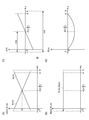
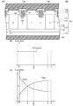
- FIG. 4A is a graph showing changes with respect to the depth of the width w n (x) at a predetermined depth position of the n- type column region and the width w p (x) at a predetermined depth position of the p-type column region
- FIG. 4B shows the depth of the average density N d (x) of positive charges at a predetermined depth position in the n-type column region and the average density N a (x) of negative charges at a predetermined depth position in the p-type column region.
- FIG. 4C is a graph showing a change with respect to the depth x of the average positive charge density ⁇ (x) at a predetermined depth position of the super junction structure
- the position where the x coordinate is d is a depth position where the average positive charge density ⁇ (x) is zero.
- the width w p (x) at the vertical position, the average density N d (x) of positive charges at a predetermined depth position of the n-type column region 114, and the average density N a of negative charges at a predetermined depth position of the p-type column region 116 (X) is a graph showing the change of the average positive charge density ⁇ (x) and the electric field E (x) with respect to the depth x at a predetermined depth position of the super junction structure 117.
- FIG. 5A is a graph showing changes of the width w n (x) at a predetermined depth position of the n-type column region 114 and the depth w of the width w p (x) at a predetermined depth position of the p-type column region 116.
- FIG. 5B shows an average density N d (x) of positive charges at a predetermined depth position in the n-type column region 114 and an average density N a (negative charge density at a predetermined depth position in the p-type column region 116.
- FIG. 5C is a graph showing a change with respect to the depth x of the average positive charge density ⁇ (x) at a predetermined depth position of the super junction structure 117.
- FIG. 5D is a graph showing the change of the electric field E (x) with respect to the depth x at a predetermined depth position of the super junction structure 117.
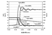
- FIG. 6 shows the time transition simulation result of the drain-source voltage Vds, drain current Id, and gate-source voltage Vgs when MOSFET is turned off.
- p-excess indicates that the total amount of impurities in the p-type column region is 10% larger than the total amount of impurities in the n-type column region
- n-excess indicates that the total amount of impurities in the n-type column region is p-type column region.
- “Just” indicates a case where the total impurity amount in the n-type column region is equal to the total impurity amount in the p-type column region (same in FIG. 7).
- the power supply voltage is 300V (the same in FIG. 7).
- 6 is a graph showing simulation results of time transitions of a drain-source voltage Vds, a drain current Id, and a gate-source voltage Vgs when a MOSFET is turned off in the power conversion circuit 1 according to the first embodiment.
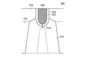
- MOSFET800 which concerns on the comparative example 1, it is a schematic diagram which shows the mode of the depletion layer of a certain moment in a turn-off period. In FIG. 8, the source region is not shown (the same is true in FIG. 9).
- MOSFET100 which concerns on Embodiment 1, it is a schematic diagram which shows the mode of the depletion layer of the moment when MOSFET is turned off.
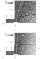
- FIG. 10A is a cross-sectional view showing a MOSFET 700 according to Comparative Example 2
- FIG. 10B is a cross-sectional view showing a MOSFET 100A according to the example.
- FIG. 10 is a schematic diagram, and does not strictly reflect the size and shape of the structure used in the simulation result of FIG.
- FIG. 10 is a diagram showing simulation results of equipotential lines when a MOSFET is turned off in MOSFET 700 according to Comparative Example 2 and MOSFET 100A according to an example.
- FIG. 10 is a schematic diagram, and does not strictly reflect the size and shape of the structure used in the simulation result of FIG.
- FIG. 11A is a diagram showing a simulation result of equipotential lines when the MOSFET is turned off in the MOSFET 700 according to the comparative example 2.
- FIG. 11B is a diagram when the MOSFET is turned off in the MOSFET 100A according to the embodiment. It is a figure which shows the simulation result of this equipotential line.
- FIG. 11A is a diagram corresponding to the region surrounded by the alternate long and short dash line in FIG. 10A
- FIG. 11B is the region surrounded by the alternate long and short dash line in FIG. It is a corresponding figure.
- FIG. 11A is a diagram corresponding to the region surrounded by the alternate long and short dash line in FIG. 10A
- FIG. 11B is the region surrounded by the alternate long and short dash line in FIG. It is a corresponding figure.
- FIG. 11A is a diagram showing a simulation result of equipotential lines when the MOSFET is turned off in the MOSFET 700 according to the comparative example 2.
- FIG. 5 is a diagram for explaining a MOSFET 102 according to a second embodiment.
- 12A is a cross-sectional view showing the MOSFET 102 according to the second embodiment.
- FIG. 12B is a predetermined depth of the n-type column region 114 when the super junction structure 117 is depleted by turning off the MOSFET.
- FIG. 12A is a cross-sectional view showing the MOSFET 102 according to the second embodiment.
- FIG. 12B is a predetermined depth of the n-type column region 114 when the super junction structure 117 is depleted by turning off the MOSFET.
- FIG. 12C is a graph showing a change of the width w n (x) at the position and the width w p (x) at the predetermined depth position of the p-type column region 116 with respect to the depth x
- FIG. is a graph showing a change with respect to the average density N depth x of a (x) of the negative charge in a predetermined depth position of the average density N d (x) and p-type column regions of positive charges at the depth position.
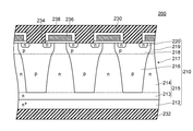
- 6 is a cross-sectional view showing a MOSFET 200 according to Embodiment 3.
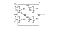
- FIG. FIG. 6 is a circuit diagram illustrating a power conversion circuit 2 according to a fourth embodiment.
- 10 is a cross-sectional view showing a MOSFET 104 according to Modification 1.
- FIG. 12 is a cross-sectional view showing a MOSFET 106 according to Modification 2.
- FIG. It is sectional drawing which shows the conventional MOSFET900.
- Reference numeral 912 indicates a low-resistance semiconductor layer
- reference numeral 913 indicates a buffer layer
- reference numeral 915 indicates an n-type semiconductor layer
- reference numeral 930 indicates a source electrode
- reference numeral 932 indicates a drain electrode.
- 10 is a cross-sectional view showing a MOSFET 902 according to Patent Document 2.
- the power conversion circuit 1 according to Embodiment 1 is a chopper circuit that is a component such as a DC-DC converter or an inverter. As shown in FIG. 1, the power conversion circuit 1 according to the first embodiment includes a reactor 10, a power supply 20, a MOSFET 100 according to the first embodiment, and a rectifying element 30.
- the reactor 10 is a passive element that can store energy in a magnetic field formed by a flowing current.
- the power source 20 is a DC power source that supplies current to the reactor 10.
- MOSFET 100 controls a current supplied from power supply 20 to reactor 10. Specifically, MOSFET 100 switches in response to a clock signal applied to the gate electrode of MOSFET 100 from a drive circuit (not shown), and when turned on, it conducts between reactor 10 and the negative electrode of power supply 20. Let me. A specific configuration of the MOSFET 100 will be described later.
- the rectifying element 30 is a fast recovery diode that performs a rectifying operation of a current supplied from the power supply 20 to the reactor 10. Specifically, the rectifying element 30 is a lifetime-controlled pin diode.
- the anode (+) of the power source 20 is electrically connected to one end 12 of the reactor 10 and the cathode electrode of the rectifying element 30, and the negative electrode ( ⁇ ) of the power source 20 is electrically connected to the source electrode of the MOSFET 100. ing.
- the drain electrode of the MOSFET 100 is electrically connected to the other end 14 of the reactor 10 and the anode electrode of the rectifying element 30.
- the current generated by the electromotive force of the reactor 10 is directed to the rectifying element 30, and a forward current flows through the rectifying element 30.
- the sum of the amount of current flowing through the MOSFET 100 and the amount of current flowing through the rectifying element 30 is equal to the amount of current flowing through the reactor 10. Since the switching period of MOSFET 100 is short (100 nsec even if estimated long), the amount of current flowing through reactor 10 hardly changes during that period. Therefore, the sum of the amount of current flowing through the MOSFET 100 and the amount of current flowing through the rectifying element 30 hardly changes in any of the on state, the turn-off period, and the off state.
- the side wall of the n-type column region 914 has a narrow tapered shape on the first main surface side, and the side wall of the p-type column region 916 has a narrow bottom.
- a MOSFET having a tapered shape for example, a conventional MOSFET 900
- the MOSFET 100 according to the first embodiment is used as the MOSFET.
- the MOSFET 100 according to Embodiment 1 includes a semiconductor substrate 110, a trench 122, a gate electrode 126, an interlayer insulating film 128, a source electrode 130, and a drain electrode.
- 132 is a trench gate type MOSFET.
- the drain-source breakdown voltage of the MOSFET 100 is 300V or more, for example, 600V.
- the semiconductor substrate 110 is formed on the n-type low-resistance semiconductor layer 112, the low-resistance semiconductor layer 112, the n-type buffer layer 113 having a lower impurity concentration than the low-resistance semiconductor layer 112, and the buffer layer 113 along the horizontal direction. And the p-type base region 118 formed on the surface of the n-type column region 114 and the p-type column region 116. And an n-type source region 120 formed on the surface of the base region 118. Note that the buffer layer 113 and the n-type column region 114 are integrally formed, and the buffer layer 113 and the n-type column region 114 constitute an n-type semiconductor layer 115.
- the total amount of impurities in the n-type column region 114 is equal to the total amount of impurities in the p-type column region 116, but may be larger than the total amount of impurities in the p-type column region 116 or less than the total amount of impurities in the p-type column region 116. Also good.
- the n-type column region 114 and the p-type column region 116 have a horizontal axis at the depth x at a predetermined depth position in the super junction structure, and the width w n (x) at the predetermined depth position in the n-type column region or the p-type column.
- the width w p (x) at a predetermined depth position of the region is taken as the vertical axis
- the width w n (x) is represented by an upward convex curve
- the width w p (x) is
- And is represented by a downwardly convex right-down curve (see FIG. 5A).
- the n-type column region 114 has a shape like a glass when viewed in cross section
- the p-type column region 116 has a shape like a trumpet when viewed in cross section.
- the impurity concentration of the n-type column region 114 and the impurity concentration of the p-type column region 116 are both constant regardless of the depth (see FIG. 5B).
- n-type column region 114, the p-type column region 116, the source region 120, the trench 122, and the gate electrode 126 are all formed in a stripe shape when seen in a plan view.
- the thickness of the low resistance semiconductor layer 112 is, for example, in the range of 100 ⁇ m to 400 ⁇ m, and the impurity concentration of the low resistance semiconductor layer 112 is, for example, in the range of 1 ⁇ 10 19 cm ⁇ 3 to 1 ⁇ 10 20 cm ⁇ 3. is there.
- the n-type semiconductor layer 115 has a thickness in the range of 5 ⁇ m to 120 ⁇ m, for example.
- the impurity concentration of the n-type semiconductor layer 115 is in the range of, for example, 5 ⁇ 10 13 cm ⁇ 3 to 1 ⁇ 10 16 cm ⁇ 3 .
- the impurity concentration of the p-type column region 116 is in the range of, for example, 5 ⁇ 10 13 cm ⁇ 3 to 1 ⁇ 10 16 cm ⁇ 3 .
- the depth position of the deepest part of the base region 118 is in the range of 0.5 ⁇ m to 4.0 ⁇ m, for example, and the impurity concentration of the base region 118 is, for example, 5 ⁇ 10 16 cm ⁇ 3 to 1 ⁇ 10 18 cm ⁇ 3. It is in the range.
- the depth position of the deepest part of the source region 120 is in the range of 0.1 ⁇ m to 0.4 ⁇ m, for example, and the impurity concentration of the source region 120 is, for example, 5 ⁇ 10 19 cm ⁇ 3 to 2 ⁇ 10 20 cm ⁇ 3. It is in the range.
- the trench 122 extends from the surface of the first main surface of the semiconductor substrate 110 to a depth deeper than the deepest part of the base region 118 in a region where the n-type column region 114 is located in plan view. A part is formed to be exposed on the inner peripheral surface.
- the depth of the trench 122 is, for example, 5 ⁇ m.
- the gate electrode 126 is embedded in the trench 122 via a gate insulating film 124 formed on the inner peripheral surface of the trench 122.
- the gate insulating film 124 is formed of a silicon dioxide film having a thickness of, for example, 100 nm formed by a thermal oxidation method.
- the gate electrode 126 is made of low resistance polysilicon formed by a CVD method and an ion implantation method.
- the interlayer insulating film 128 is formed so as to cover a part of the source region 120, the gate insulating film 124 and the gate electrode 126.
- the interlayer insulating film 128 is made of a PSG film having a thickness of, for example, 1000 nm formed by a CVD method.
- the source electrode 130 is formed so as to cover the base region 118, a part of the source region 120, and the interlayer insulating film 128, and is electrically connected to the source region 120.
- the drain electrode 132 is formed on the surface of the low resistance semiconductor layer 112.
- the source electrode 130 is made of an aluminum-based metal (for example, an Al—Cu-based alloy) having a thickness of, for example, 4 ⁇ m formed by a sputtering method.
- the drain electrode 132 is formed of a multilayer metal film such as Ti—Ni—Au. The total thickness of the multilayer metal film is, for example, 0.5 ⁇ m.
- Depth of a predetermined depth position in the super junction structure 117 with reference to the deepest depth position of the surface of the depletion layer on the first main surface side when the MOSFET is turned off and the depletion layer spreads most in the super junction structure.
- x hereinafter simply referred to as depth x
- the average positive charge density ⁇ (x) is expressed by the following equation (1).
- w n (x) indicates the width of the n-type column region 114 at a predetermined depth position
- N d (x) indicates that when the MOSFET is turned off and the super junction structure 117 is depleted.
- the average density of positive charges at a predetermined depth position of the n-type column region 114, w p (x) indicates the width at the predetermined depth position of the p-type column region, and N a (x) indicates the MOSFET Is turned off and the super junction structure 117 is depleted, the average density of negative charges at a predetermined depth position of the p-type column region 116, q indicates the amount of electric charge, and w indicates w n (x ) + W p (x) a positive constant that satisfies 2w (see FIG. 3)
- an electric field E (x) at a predetermined depth position of the super junction structure 117 turns the MOSFET off.
- an electric field generated from a positive charge (donor) at a predetermined depth position of the n-type column region 114 and a negative charge (acceptor) at a predetermined depth position of the p-type column region 116 Is represented by the following formula (3).
- ⁇ represents the dielectric constant of the semiconductor substrate material (eg, silicon).
- MOSFET 800 (see FIG. 8) according to Comparative Example 1 basically has the same configuration as MOSFET 100 according to the first embodiment, but the sidewall of n-type column region 814 is the same as that of conventional MOSFET 900.
- the main surface side has a narrow tapered shape, and the side wall of the p-type column region 816 differs from the MOSFET 100 according to the first embodiment in that the bottom has a narrow tapered shape.
- the depth x is the horizontal axis, and the width w n (x) at the predetermined depth position of the n-type column region 814 or the width w p (at the predetermined depth position of the p-type column region 816).
- x is the vertical axis
- the width w p (x) is represented by a straight line that descends to the right
- the width w n (x) is represented by a straight line that rises to the right (FIG. 4A). reference.).
- the impurity concentration in the n-type column region 814 and the impurity concentration in the p-type column region 816 are constant regardless of the depth (FIG. 4). (See (b).)
- average positive charge density (rho) (x) is represented by the straight line going up to the right (refer FIG.4 (c)). Looking at the straight line representing the average positive charge density ⁇ (x) in detail, the deepest depth position of the surface of the depletion layer on the first main surface side when the MOSFET is turned off and the depletion layer spreads most in the super junction structure.
- the axis along the depth direction is the x axis
- the x coordinate of the depth position of the bottom surface of the base region is -t
- the x coordinate of the depth position of the bottom portion of the p-type column region is b
- the surface of the depletion layer on the second main surface side when the x coordinate of the depth position where the average positive charge density ⁇ (x) becomes 0 is d, the MOSFET is turned off and the depletion layer spreads most in the super junction structure
- the x coordinate of the shallowest depth position is a, the following (1) to (3) hold.
- (1) Satisfy d a / 2.
- the depth at which the average positive charge density ⁇ (x) becomes 0 is the surface of the depletion layer on the first main surface side when the MOSFET is turned off and the depletion layer spreads most in the super junction structure.
- the depth d at a predetermined depth position when the average positive charge density ⁇ (x) is 0 when the deepest depth position is used as a reference is determined by turning off the MOSFET and providing a depletion layer in the super junction structure.
- the width x at the predetermined depth position of the n- type column region or the width at the predetermined depth position of the p-type column region with the depth x as the horizontal axis When w p (x) is the vertical axis, the width w n (x) is represented by a monotonically rising curve that is convex upward, and the width w p (x) is monotonous that is convex downward. It is represented by a straight downward curve (see FIG. 5A).
- the impurity concentration of the n-type column region 114 and the impurity concentration of the p-type column region 116 are constant regardless of the depth (see FIG. 5B).
- the average positive charge density ⁇ (x) is represented by a monotonically rising curve that is convex upward (see FIG. 5C). Looking at the curve representing the average positive charge density ⁇ (x) in detail, the deepest depth position of the surface of the depletion layer on the first main surface side when the MOSFET is turned off and the depletion layer spreads most in the super junction structure.
- the axis along the depth direction is the x axis
- the x coordinate of the depth position of the bottom surface of the base region is -t
- the x coordinate of the depth position of the bottom portion of the p-type column region is b
- the surface of the depletion layer on the second main surface side when the x coordinate of the depth position where the average positive charge density ⁇ (x) becomes 0 is d, the MOSFET is turned off and the depletion layer spreads most in the super junction structure If the x coordinate of the shallowest depth position is a, the following (1) to (4) hold. (1) 0 ⁇ d ⁇ a / 2 is satisfied.
- the average positive charge density ⁇ (x The depth d at a predetermined depth position when the) becomes 0 is the shallowest depth of the surface of the depletion layer on the second main surface side when the MOSFET is turned off and the depletion layer spreads most in the super junction structure. It is shallower than half the depth a of the position. (That is, the depth position where charge balance is achieved is shallower than the depth position where charge balance is achieved in MOSFET 800 according to Comparative Example 1).
- the MOSFET 800 according to the comparative example 1 operates as follows. .
- Drain current Id When the total amount of impurities in the n-type column region is equal to the total amount of impurities in the p-type column region (hereinafter referred to as Just), the drain current Id starts to decrease until the drain current Id first becomes zero. It operates so that the period during which the drain current Id rises temporarily appears slightly (operates so that the bump waveform appears slightly in the waveform of the drain current Id. See Id (Just) in FIG. 6).
- the period from when the drain current Id starts to decrease until the drain current Id first becomes 0 is about 0.02 usec (20 nsec).
- excessive n the drain current Id starts after the drain current Id starts to decrease. 6 is operated so that a period in which the drain current Id rises temporarily appears until the first becomes 0 (the operation is such that a large bump waveform appears in the waveform of the drain current Id. (Refer to n excess).
- the drain current Id increases to a higher current value than in the case of Just, and the period until the drain current Id becomes 0 is significantly longer than in Just (the case of Just is about (In contrast to 0.02 usec (20 nsec), it is about 0.04 usec (40 nsec) when n is excessive).
- the drain current Id operates so as to monotonously decrease (in the waveform of the drain current Id). The operation is performed so that the bump waveform does not appear (see Id (excessive p) in FIG. 6).
- drain-source voltage Vds Drain-source voltage Vds
- the time required for the drain-source voltage Vds to rise and stabilize is about 0.05 usec (50 nsec) longer than Just (see Vds (n excess) in FIG. 6).
- the drain-source voltage Vds increases to about 370 V more rapidly than in the case of Just, and then operates to stabilize at the power supply voltage (300 V) (see Vds (excessive p) in FIG. 6).
- the time required for the drain-source voltage Vds to rise and stabilize is about 0.02 usec (20 nsec).
- Gate-source voltage Vgs When n is excessive, the gate-source voltage Vgs operates so that a period of temporary increase after the end of the mirror period appears slightly (see Vgs (n excessive) in FIG. 6). On the other hand, in the case of Just and excessive p, the gate-source voltage Vgs hardly changes and operates so as to decrease monotonously (see Vgs (excessive p) and Vgs (Just) in FIG. 6).
- the MOSFET 100 operates as follows. (1) Drain current Id In the case of Just, in all cases of n excess and p excess, the turn-off period is shortened, and the operation is performed so that a similar waveform is obtained in any case (see each Id in FIG. 7). In particular, when n is excessive, the bump waveform hardly appears in the waveform of the drain current Id, and operates so as to be close to the waveforms in the case of Just and excessive p.
- Drain-source voltage Vds In the case of Just, in all cases of n excess and p excess, the turn-off period is shortened, and the operation is performed so that a similar waveform is obtained in any case (see each Vds in FIG. 7). When p is excessive, ringing occurs. This ringing can be reduced by providing a mechanism for removing ringing such as a snubber circuit.
- Gate-source voltage Vgs In the case of Just, the operation is performed so that there is almost no difference in the waveform of the gate-source voltage Vgs in all cases of excessive n and excessive p (see Vgs in FIG. 7).
- the reason why the waveforms of the MOSFET 100 according to the first embodiment and the MOSFET 800 according to the comparative example 1 are as described above when the MOSFET is turned off will be described.
- the depletion layer from the pn junction between the p-type column region 816 (and the base region 818) and the n-type column region 814 becomes the n-type column region 814 and the p-type.
- the column area 816 extends.
- MOSFET 800 according to Comparative Example 1 since the depletion layer is difficult to spread to the drain electrode side (although the depletion layer extends just below the trench), the distance between the non-depleted region in n-type column region 814 and gate electrode 826 Is difficult to lengthen, and it is difficult to reduce the feedback capacitance Crss (see FIG. 8). Therefore, the gate electrode 826 is easily affected by the potential change in the n-type column region 814, and when there is a variation in charge balance around the gate, it is difficult to reduce the variation in switching characteristics when the gate is turned off.
- the depletion layer easily spreads to the drain electrode side, the interval between the non-depleted region in the n-type column region 114 and the gate electrode 126 can be easily increased. It becomes easy to reduce the feedback capacitance Crss (see FIG. 9). For this reason, the gate electrode 126 can be hardly affected by the potential change of the n-type column region 114, and when there is a variation in charge balance around the gate, the variation in switching characteristics when turned off can be reduced. it can.
- the MOSFET 700 according to the comparative example 2 is a MOSFET having the same configuration as that of the MOSFET 800 according to the comparative example 1 except that a portion in contact with the source electrode is dug up to the lowest depth position of the source region. (See FIG. 10A.)
- the MOSFET 100A according to the example is the same as the MOSFET 100 according to the first embodiment except that the portion in contact with the source electrode is dug up to the lowest depth of the source region. This is a MOSFET having a similar configuration (see FIG. 10B).
- the MOSFET 700 according to the comparative example 2 when the MOSFET is turned off, the interval between the equipotential lines at the bottom of the trench is in a narrow state (see FIG. 11A). This is because the distance between the non-depleted region in the n-type column region 714 and the gate electrode 726 is short. Therefore, the potential gradient in the vicinity of the bottom of the trench is increased, and the gate electrode 726 is easily affected by the potential change in the n-type column region 714. Therefore, when there is a variation in charge balance around the gate, it is difficult to reduce the variation in switching characteristics when turned off.
- the interval between the equipotential lines near the bottom of the trench 122 is wide (see FIG. 11B). This is because the distance between the non-depleted region in the n-type column region 114 and the gate electrode 126 is long. As a result, the potential gradient near the bottom of the trench 122 is reduced, and the gate electrode 126 is less susceptible to the potential change of the n-type column region 114. Therefore, even if there is a variation in charge balance around the gate, the variation in switching characteristics when turned off can be reduced.
- ⁇ (x) is smaller than the conventional MOSFET 900 (larger in the negative side), and the difference between the negative charge amount of the p-type column region 116 and the positive charge amount of the n-type column region 114 is larger than that of the conventional MOSFET 900. growing. Therefore, (1) since the n-type column region 114 around the gate is more easily depleted than the conventional MOSFET 900, the potential of the n-type column region 114 around the gate is hardly increased even if the drain voltage is increased.
- the distance between the non-depleted region in the n-type column region 114 and the gate electrode 126 is longer than that of the conventional MOSFET 900, and the feedback capacitance Crss (equal to the gate-drain capacitance Cgd) is increased. Therefore, even when the potential of the n-type column region 114 (the non-depleted region of the n-type column region 114) increases as the drain voltage increases when the MOSFET is turned off, The gate electrode 126 is not easily affected by the potential change in the n-type column region 114. As a result, even if there is a variation in charge balance around the gate, the variation in switching characteristics when turned off can be made smaller than before.
- the average positive charge density ⁇ (x) at a predetermined depth position of the super junction structure 117 when the MOSFET is turned off and the super junction structure 117 is depleted is Since it is represented by a convex upward curve, the average positive charge density ⁇ (x) is small (large on the negative side) at the depth position around the gate, and the negative charge amount of the p-type column region 116 is small. It becomes larger than the positive charge amount of the n-type column region. Therefore, the holes around the gate can be easily pulled out by the negative charge of the p-type column region 116, and as a result, the L load avalanche breakdown resistance can be increased.
- the MOSFET 100 includes the semiconductor substrate 110 having the super junction structure 117 composed of the n-type column region 114 and the p-type column region 116. Therefore, as in the case of the conventional MOSFET 900, the low-power The switching element has an on-resistance and a high breakdown voltage.
- the deepest depth position of the surface of the depletion layer on the first main surface side when the MOSFET is turned off and the depletion layer spreads most in super junction structure 117 is used as a reference.
- the depth of the shallowest depth position of the surface of the depletion layer on the second main surface side is defined as a, and the average in the super junction structure 117 In order to satisfy 0 ⁇ d ⁇ a / 2, where d is the depth at which the positive charge density ⁇ (x) becomes 0, the negative charge of the p-type column region 116 at the depth around the gate.
- the difference between the amount of charges in the n-type column region 114 and the amount of positive charges in the n-type column region 114 increases, and the n-type column region 114 around the gate tends to be depleted. Even if there is variation in the charge balance of the peripheral bets can be further reduced the variance of the switching characteristic when turned off.
- the horizontal axis is the depth x at the predetermined depth position in the super junction structure 117, and the width w n (x) at the predetermined depth position in the n-type column region 114 or the p-type.
- the width w p (x) at a predetermined depth position of the column region 116 is the vertical axis
- the width w p (x) is represented by a downwardly convex right-down curve
- the width w n (x ) Is represented by an upwardly convex upward curve
- the MOSFET 100 according to the first embodiment is a trench gate type MOSFET. With such a configuration, even when a trench gate type MOSFET is turned off, the gate electrode and the drain electrode are closer than the planar gate type MOSFET and the potential of the n-type column region 114 around the gate is likely to rise. The variation in the switching characteristics can be made smaller than in the conventional case.
- the deepest depth position of the surface of the depletion layer on the first main surface side when the MOSFET is turned off and the depletion layer spreads most in super junction structure 117 is used as a reference.
- the axis along the depth direction is the x axis
- the x coordinate of the depth position of the bottom surface of the base region 11 is -t
- the x coordinate of the depth position of the bottom portion of the p-type column region 116 is b
- the gate periphery is also obtained by such a configuration.
- the difference between the negative charge amount of the p-type column region 116 and the positive charge amount of the n-type column region 114 becomes large at the depth position, and the n-type column region 114 around the gate tends to be depleted. As a result, even if there is a variation in charge balance around the gate, the variation in switching characteristics when turned off can be further reduced.
- the rectifying element is a fast recovery diode
- the turn-off period is short, and when the MOSFET is turned off, the potential of the n-type column region 114 increases with the drain voltage. Is difficult to rise. Therefore, it is difficult for the potential of the gate electrode to rise, and as a result, even if there is a variation in the charge balance around the gate, the variation in switching characteristics when turned off can be made smaller than in the prior art.
- the MOSFET 102 according to the second embodiment basically has the same configuration as the MOSFET 100 according to the first embodiment, but the width w n (x) at a predetermined depth position of the n-type column region and the predetermined depth of the p-type column region. Instead of the width w p (x) at the vertical position, the average density N d (x) of positive charges at a predetermined depth position of the n-type column region when the MOSFET is turned off and the super junction structure is depleted, and This is different from the MOSFET 100 according to the first embodiment in that the negative charge average density N a (x) at a predetermined depth position in the p-type column region is changed.
- the average density N d (x) of positive charges at the predetermined depth position of the n-type column region 114 and the p-type with the depth x as the horizontal axis is taken as the vertical axis
- the average density N d (x) of the positive charges is a monotonically rising curve that is convex upward.
- the average density N a (x) of the negative charge is represented by a monotonous downwardly convex curve (see FIG. 12C). Note that the width of the n-type column region 114 and the width of the p-type column region 116 are both constant regardless of the depth (see FIG. 12B).
- the MOSFET 102 according to the second embodiment is different from the width w p (x) at the predetermined depth position of the p- type column region and the width w n (x) at the predetermined depth position of the n-type column region.
- the MOSFET 100 according to the first embodiment differs from the MOSFET 100 according to the first embodiment in that the density N a (x) is changed, like the MOSFET 100 according to the first embodiment, the MOSFET is turned off and the super junction structure 117 is depleted.
- the average positive charge density ⁇ (x) at a predetermined depth position of the super junction structure 117 rises upward to the right Therefore, in the depth position around the gate (region where x is close to 0), the average positive charge density ⁇ (x) is smaller than that of the conventional MOSFET 900 (larger on the negative side), and is p-type.
- the difference between the negative charge amount of the column region 116 and the positive charge amount of the n-type column region 114 is larger than that of the conventional MOSFET 900. Therefore, (1) since the n-type column region 114 around the gate is more easily depleted than the conventional MOSFET 900, the potential of the n-type column region 114 around the gate is hardly increased even if the drain voltage is increased.
- the distance between the non-depleted region in the n-type column region 114 and the gate electrode 126 becomes longer, and the feedback capacitance Crss becomes smaller than that of the conventional MOSFET 900, so that the drain voltage is reduced when the MOSFET is turned off.
- the gate electrode 126 is affected by the potential change of the n-type column region 114. It becomes difficult. Therefore, even if there is a variation in charge balance around the gate, the variation in switching characteristics when turned off can be made smaller than in the prior art.
- the MOSFET 102 turns off the MOSFET, not the width w n (x) at the predetermined depth position of the n- type column region and the width w p (x) at the predetermined depth position of the p-type column region.
- the average density N d (x) of positive charges at a predetermined depth position of the n-type column region and the average density N of negative charges at a predetermined depth position of the p-type column region Since it has the same configuration as the MOSFET 100 according to the first embodiment except for the point where a (x) is changed, the corresponding effect among the effects of the MOSFET 100 according to the first embodiment is obtained.
- the MOSFET 200 according to the third embodiment basically has the same configuration as the MOSFET 100 according to the first embodiment.
- the MOSFET 200 according to the first embodiment is not a trench gate type MOSFET but a planar gate type MOSFET. Is different. That is, in the MOSFET 200 according to the third embodiment, as shown in FIG. 13, the semiconductor substrate 210 includes the entire surface of the first main surface of the semiconductor substrate 210 and the surface of the p-type column region 216 and the n-type column region.
- the gate insulating film 234 is formed on the surface of the region 218.
- the depth position of the n-type surface high concentration region 219 is in the range of 1.0 ⁇ m to 4.0 ⁇ m, and the impurity concentration of the n-type surface high concentration region 219 is 1 ⁇ 10 14 cm ⁇ 3 to 1 ⁇ . It is in the range of 10 16 cm ⁇ 3 .
- the MOSFET 200 according to the third embodiment is different from the MOSFET 100 according to the first embodiment in that it is not a trench gate type MOSFET but a planar gate type MOSFET.
- the MOSFET is turned off and the super junction structure 217 is depleted, the average positive charge density ⁇ (x) at a predetermined depth position of the super junction structure 217 is expressed by an upwardly convex upward curve.
- the average positive charge density ⁇ (x) is smaller (larger on the negative side) than the conventional MOSFET 900, and the p-type column region 216
- the difference between the negative charge amount and the positive charge amount of the n-type column region 214 is the conventional MOSFE. It becomes larger than T900. Therefore, (1) the n-type column region 214 around the gate is more easily depleted than in the conventional MOSFET, so that the potential of the n-type column region 214 around the gate is not easily increased even if the drain voltage is increased.
- the distance between the non-depleted region in the n-type column region 214 and the gate electrode 236 becomes longer, and the feedback capacitance Crss becomes smaller than that of the conventional MOSFET, so that the drain voltage is reduced when the MOSFET is turned off.
- the gate electrode 236 is affected by the potential change of the n-type column region 214. It becomes difficult. Therefore, even if there is a variation in charge balance around the gate, the variation in switching characteristics when turned off can be made smaller than in the prior art.
- the MOSFET 200 according to the third embodiment has the same configuration as that of the MOSFET 100 according to the first embodiment except that the MOSFET 200 is not a trench gate type MOSFET but a planar gate type MOSFET. This has a corresponding effect among the effects of the MOSFET 100.
- the power conversion circuit 2 according to the fourth embodiment basically has the same configuration as that of the power conversion circuit 1 according to the first embodiment, but the MOSFET 100 according to the first embodiment is different in that the power conversion circuit is a full bridge circuit. Not the case. That is, as shown in FIG. 14, the power conversion circuit 2 according to the fourth embodiment includes four MOSFETs 100 (100a to 100d) as MOSFETs, and includes a built-in diode of each MOSFET as a rectifier.
- the power conversion circuit 2 according to the fourth embodiment is different from the power conversion circuit 1 according to the first embodiment in that the power conversion circuit is a full bridge circuit, but the power conversion circuit according to the first embodiment.
- the average positive charge density ⁇ (x) at a predetermined depth position of the superjunction structure 117 is an upward convex upward Since it is represented by a curve, the average positive charge density ⁇ (x) is smaller (larger on the negative side) than the conventional MOSFET 900 at the depth position around the gate (region where x is close to 0), and the p-type column
- the difference between the amount of negative charges in the region 116 and the amount of positive charges in the n-type column region 114 is larger than that of the conventional MOSFET 900.
- the n-type column region 114 around the gate is more easily depleted than in the conventional MOSFET, the potential of the n-type column region 114 around the gate is not easily increased even if the drain voltage is increased. Also, (2) the distance between the non-depleted region in the n-type column region 114 and the gate electrode 126 becomes longer, and the feedback capacitance Crss becomes smaller than that of the conventional MOSFET, so that the drain voltage is reduced when the MOSFET is turned off. Even if the potential of the n-type column region 114 (the non-depleted region of the n-type column region) increases with the increase, the gate electrode 126 is affected by the potential change of the n-type column region 114. It becomes difficult. Therefore, even if there is a variation in charge balance around the gate, the variation in switching characteristics when turned off can be made smaller than in the prior art.
- the power conversion circuit 2 when the superjunction structure 117 is depleted by turning off the MOSFET, the average positive charge density ⁇ (x) at a predetermined depth position of the superjunction structure 117 is Therefore, as described above, the n-type column region 114 (depletion in the n-type column region 114 is accompanied by an increase in drain voltage when the MOSFET is turned off. Even if the potential of the non-converted region) rises, the gate electrode 126 becomes difficult to be affected by the potential change of the n-type column region 114. For this reason, a phenomenon called false turn-on (false ON) hardly occurs.
- false turn-on is that when one of the MOSFETs is turned on in a circuit in which two or more MOSFETs are connected, the other MOSFET is erroneously turned on due to a potential change. It is a phenomenon.
- the rectifying element is a MOSFET built-in diode, it is not necessary to prepare a rectifying element separately.
- the power conversion circuit 2 according to the fourth embodiment has the same configuration as that of the power conversion circuit 1 according to the first embodiment except that the power conversion circuit is a full bridge circuit. It has a corresponding effect among the effects which the power converter circuit 1 has.
- the width w n (x) at a predetermined depth position of the n-type column region is represented by a monotonically rising curve that is convex upward, and the predetermined width of the p-type column region
- the width w p (x) at the depth position is represented by a monotonous downwardly convex curve convex downward, the present invention is not limited to this.
- the width w n (x) at a predetermined depth position of the n-type column region is changed to a monotonically rising curve with a staircase shape (however, a line connecting the corner portions of the staircase (envelope) is convex upward)
- the width w p at a predetermined depth position of the p-type column region is a monotonous right-down step with a staircase shape (however, a line connecting the corners of the staircase (envelope) is convex downward)
- the width w n (x) at a predetermined depth position of the n-type column region is a curve that repeats unevenness (provided that the envelope is monotonous upward)
- the width w p at the predetermined depth position of the p-type column region is a curve that repeats unevenness (provided that the envelope curve is a monotonous downward curve with a downward convexity). ) (See FIG. 16).
- the average density N d (x) of positive charges at a predetermined depth position in the n-type column region is represented by a monotonically rising curve that is convex upward. It is not limited to.
- the average density N d (x) of positive charges at a predetermined depth position in the n-type column region is changed to a monotonous curve with a stepped shape (however, a line connecting the corners of the steps is convex upward). Or a curve that repeats unevenness (however, the envelope becomes a monotonically rising curve with a convex upward shape).
- the average density N a (x) of negative charges at a predetermined depth position of the p-type column region is represented by a monotonically downward-declining curve that protrudes downward. It is not limited to.
- the average density N a (x) of negative charges at a predetermined depth position in the p-type column region is changed to a stepwise shape (however, a line connecting the corners of the steps is a monotonous downward-sloping curve that protrudes downward). It may be expressed by a curve that repeats unevenness (however, the envelope becomes a monotonous, downward-sloping curve that protrudes downward).
- the n-type column region 114, the p-type column region 116, the trench 122, and the gate electrode 126 are formed in a stripe shape as viewed in plan, but the present invention is not limited to this. is not.
- the n-type column region 114, the p-type column region 116, the trench 122, and the gate electrode 126 are viewed in a plan view so as to have a circular shape (a columnar shape when viewed three-dimensionally), a quadrangular frame shape, a circular frame shape, or a lattice shape. It may be formed.
- a DC power source is used as the power source, but the present invention is not limited to this.
- An AC power source may be used as the power source.
- a chopper circuit is used as the power conversion circuit.
- a full bridge circuit is used as the power conversion circuit.
- the present invention is not limited to this. Absent.
- a half bridge circuit a three-phase AC converter, a non-insulated full bridge circuit, a non-insulated half bridge circuit, a push-pull circuit, an RCC circuit, a forward converter, a flyback converter, or other circuits may be used.
- a pin diode is used as the rectifying element.
- a MOSFET built-in diode is used.
- the present invention is not limited to this.
- JBS, MPS or other fast recovery diode, silicon carbide Schottky barrier diode or other diode may be used.
- n-type semiconductor layer 116, 216, 716, 816, 916 ... p-type column region, 117, 217, 717, 917 ... super junction structure 118, 218, 718, 818, 918 ... base region, 219, 919 ... n-type surface high concentration 120, 220, 720, 920 ... source region, 122, 722, 822 ... trench, 124, 234, 724, 824, 934 ... gate insulating film, 126, 236, 726, 826, 936 ... gate electrode, 128, 238, 728 ... interlayer insulating film, 130, 230, 730, 930 ... source electrode, 132, 232, 732, 932 ... drain electrode
Landscapes
- Engineering & Computer Science (AREA)
- Power Engineering (AREA)
- Insulated Gate Type Field-Effect Transistor (AREA)
- Metal-Oxide And Bipolar Metal-Oxide Semiconductor Integrated Circuits (AREA)
- Dc-Dc Converters (AREA)
- Electrodes Of Semiconductors (AREA)
- Inverter Devices (AREA)
Abstract
本発明のMOSFET100は、スーパージャンクション構造117を有する半導体基体110と、半導体基体110の第1主面側にゲート絶縁膜124を介して形成されたゲート電極126とを備え、スーパージャンクション構造117における所定深さ位置の深さxを横軸とし、スーパージャンクション構造117の所定深さ位置における平均正電荷密度ρ(x)を縦軸としたときに、MOSFETをターンオフしてスーパージャンクション構造117が空乏化したときの、スーパージャンクション構造117の所定深さ位置における平均正電荷密度ρ(x)は、上に凸の右上がりの曲線で表されることを特徴とする。 本発明のMOSFET100によれば、ゲート周辺のチャージバランスのバラツキがあったとしても、ターンオフしたときのスイッチング特性のバラツキを従来よりも小さくすることができる。
Description
本発明は、MOSFET及び電力変換回路に関する。
従来、n型コラム領域及びp型コラム領域から構成されたスーパージャンクション構造を有する半導体基体を備えるMOSFETが知られている(例えば、特許文献1参照。)。
なお、本明細書中、スーパージャンクション構造とは、所定の断面で見たときにn型コラム領域とp型コラム領域とが交互に繰り返し配列されている構造をいう。
従来のMOSFET900は、図17に示すように、n型コラム領域914及びp型コラム領域916から構成されたスーパージャンクション構造917と、第1主面の表面、かつ、p型コラム領域916の表面上の全部及びn型コラム領域914の表面上の一部に形成されたベース領域918と、第1主面の表面、かつ、n型コラム領域914の表面上にベース領域918に隣接するように形成されたn型表面高濃度領域919と、ベース領域918の表面に形成されたn型のソース領域920とを有する半導体基体910と、ソース領域920とn型表面高濃度領域919とに挟まれたベース領域918の表面上にゲート絶縁膜934を介して形成されたゲート電極936とを備えるプレーナーゲート型のMOSFETである。
従来のMOSFET900において、n型コラム領域914及びp型コラム領域916は、n型コラム領域914の不純物総量とp型コラム領域916の不純物総量とが等しくなるように形成されている。すなわち、n型コラム領域914及びp型コラム領域916は、チャージバランスが取れている。また、n型コラム領域914の不純物濃度及びp型コラム領域916の不純物濃度はいずれも、深さによらず一定となっている。さらにまた、n型コラム領域914の側壁は、第1主面側が狭いテーパ形状となっており、p型コラム領域916の側壁は、底が狭いテーパ形状となっている。
なお、本明細書中、「不純物総量」とは、MOSFET内の構成要素(n型コラム領域又はp型コラム領域)の不純物の総量をいう。
従来のMOSFET900は、n型コラム領域914及びp型コラム領域916から構成されたスーパージャンクション構造917を有する半導体基体910を備えるため、低オン抵抗、かつ、高耐圧のスイッチング素子となる。
ところで、従来のMOSFET900においては、ゲート周辺のチャージバランスにバラツキがあると、ターンオフしたときのスイッチング特性のバラツキが大きくなる、という問題がある。
そこで、本発明は、上記した問題を解決するためになされたものであり、ゲート周辺のチャージバランスのバラツキがあったとしても、ターンオフしたときのスイッチング特性のバラツキを従来よりも小さくできるMOSFET及びこれを用いた電力変換回路を提供することを目的とする。
[1]本発明のMOSFETは、n型コラム領域及びp型コラム領域から構成されたスーパージャンクション構造を有する半導体基体と、前記半導体基体の第1主面側にゲート絶縁膜を介して形成されたゲート電極とを備えるMOSFETであって、前記MOSFETをターンオフして前記スーパージャンクション構造に空乏層が最も広がったときの前記第1主面側の空乏層の表面のうち最も深い深さ位置を基準として、前記MOSFETをターンオフしてスーパージャンクション構造が空乏化したときの、前記スーパージャンクション構造における所定深さ位置の深さxを横軸とし、前記MOSFETをターンオフして前記スーパージャンクション構造が空乏化したときの、以下の式(1)で表される、前記スーパージャンクション構造の前記所定深さ位置における平均正電荷密度ρ(x)を縦軸としたときに、当該平均正電荷密度ρ(x)は、上に凸の右上がりの曲線で表されており、前記MOSFETをターンオフして前記スーパージャンクション構造に空乏層が最も広がったときの前記第1主面側の空乏層の表面のうち最も深い深さ位置を基準として、前記MOSFETをターンオフして前記スーパージャンクション構造に空乏層が最も広がったときの第2主面側の空乏層の表面のうち最も浅い深さ位置の深さをaとしたときに、x=0のときの当該平均正電荷密度ρ(0)の値が負であり、かつ、x=aのときの当該平均正電荷密度ρ(a)の値が正であり、当該平均正電荷密度ρ(x)を表す曲線、x=0の直線及び前記横軸で囲まれた領域の面積は、当該平均正電荷密度ρ(x)を表す曲線、x=aの直線及び前記横軸で囲まれた領域の面積と等しいことを特徴とするMOSFET。

(式(1)中、wn(x)は、前記n型コラム領域の前記所定深さ位置における幅を示し、Nd(x)は、前記MOSFETをターンオフして前記スーパージャンクション構造が空乏化したときの、前記n型コラム領域の前記所定深さ位置における正電荷の平均密度を示し、wp(x)は、前記p型コラム領域の前記所定深さ位置における幅を示し、Na(x)は、前記MOSFETをターンオフして前記スーパージャンクション構造が空乏化したときの、前記p型コラム領域の前記所定深さ位置における負電荷の平均密度を示し、qは、電気素量を示し、wは、wn(x)+wp(x)=2wを満たす正の定数を示す。)
なお、本明細書中、「スーパージャンクション構造における所定深さ位置の深さ」とは、MOSFETをターンオフしてスーパージャンクション構造に空乏層が最も広がったときの第1主面側の空乏層の表面のうち最も深い深さ位置を基準としたスーパージャンクション構造内の所定の深さ位置の深さのことをいう。従って、MOSFETをターンオフしてスーパージャンクション構造に空乏層が最も広がったときの第1主面側の空乏層の表面のうち最も深い深さ位置においては、当該深さxは0になる。また、「第2主面」とは、第1主面とは反対側の主面のことをいう。また、「n型コラム領域の・・・正電荷の平均密度」は、MOSFETをターンオフしてn型コラム領域が空乏化したときの、n型コラム領域のドナーに起因した正電荷の平均密度を示し、「p型コラム領域の・・・負電荷の平均密度」は、MOSFETをターンオフしてp型コラム領域が空乏化したときの、p型コラム領域のアクセプタに起因した負電荷の平均密度を示す。さらにまた、「スーパージャンクション構造の所定深さ位置における平均正電荷密度ρ(x)は、上に凸の右上がりの曲線で表される」とは、当該平均正電荷密度が上に凸の単調な右上がりの曲線で表される場合のみならず、当該平均正電荷密度が階段状(但し、階段の角の部分を結んだ線(包絡線)が上に凸の単調な右上がりの曲線になる)で表される場合や、当該平均正電荷密度が凹凸を繰り返す曲線(但し、包絡線が上に凸の単調な右上がりの曲線になる)で表される場合を含むものとする。
[2]本発明のMOSFETにおいては、前記MOSFETをターンオフして前記スーパージャンクション構造に空乏層が最も広がったときの前記第1主面側の空乏層の表面のうち最も深い深さ位置を基準として、前記MOSFETをターンオフして前記スーパージャンクション構造に空乏層が最も広がったときの前記第2主面側の空乏層の表面のうち最も浅い深さ位置の深さをaとし、前記スーパージャンクション構造における、前記平均正電荷密度ρ(x)が0になる深さ位置の深さをdとしたときに、0<d<a/2を満たすことが好ましい。
[3]本発明のMOSFETにおいては、前記スーパージャンクション構造における前記所定深さ位置の深さxを横軸とし、前記n型コラム領域の前記所定深さ位置における幅wn(x)又は前記p型コラム領域の前記所定深さ位置における幅wp(x)を縦軸としたときに、前記n型コラム領域の前記所定深さ位置における幅wn(x)は、上に凸の右上がりの曲線で表され、前記p型コラム領域の前記所定深さ位置における幅wp(x)は、下に凸の右下がりの曲線で表されることが好ましい。
[4]本発明のMOSFETにおいては、前記スーパージャンクション構造における所定深さ位置の深さxを横軸とし、前記MOSFETをターンオフして前記スーパージャンクション構造が空乏化したときの、前記n型コラム領域の前記所定深さ位置における正電荷の平均密度Nd(x)又は前記p型コラム領域の前記所定深さ位置における負電荷の平均密度Na(x)を縦軸としたときに、前記MOSFETをターンオフして前記スーパージャンクション構造が空乏化したときの、前記n型コラム領域の前記所定深さ位置における正電荷の平均密度Nd(x)は、上に凸の右上がりの曲線で表され、前記MOSFETをターンオフして前記スーパージャンクション構造が空乏化したときの、前記p型コラム領域の前記所定深さ位置における負電荷の平均密度Na(x)は、下に凸の右下がりの曲線で表されることが好ましい。
[5]本発明のMOSFETにおいては、前記半導体基体は、前記n型コラム領域及び前記p型コラム領域の表面上に形成されたp型のベース領域と、前記ベース領域の表面に形成されたn型のソース領域とをさらに有し、前記MOSFETは、平面的に見て前記n型コラム領域が位置する領域内において、前記半導体基体の第1主面の表面から前記ベース領域の最深部よりも深い深さ位置まで、かつ、前記ソース領域の一部が内周面に露出するように形成されたトレンチをさらに備え、前記ゲート絶縁膜は、前記トレンチの内周面に形成されており、前記ゲート電極は、前記ゲート絶縁膜を介して前記トレンチの内部に埋め込まれてなることが好ましい。
[6]本発明のMOSFETにおいては、前記半導体基体は、前記半導体基体の前記第1主面の表面、かつ、前記p型コラム領域の表面上の全部及び前記n型コラム領域の表面上の一部に形成されたベース領域と、前記半導体基体の前記第1主面の表面、かつ、前記n型コラム領域の表面上に前記ベース領域に隣接するように形成されたn型表面高濃度領域と、前記ベース領域の表面に形成されたn型のソース領域とをさらに有し、前記ゲート電極は、前記ソース領域と前記n型表面高濃度領域とに挟まれた前記ベース領域の表面上に前記ゲート絶縁膜を介して形成されていることが好ましい。
[7]本発明のMOSFETにおいては、前記MOSFETをターンオフして前記スーパージャンクション構造に空乏層が最も広がったときの前記第1主面側の空乏層の表面のうち最も深い深さ位置を基準として、深さ方向に沿った軸をx軸とし、前記ベース領域の最下面の深さ位置のx座標を-tとし、前記p型コラム領域の最下部の深さ位置のx座標をbとし、前記平均正電荷密度ρ(x)が0になる深さ位置のx座標をdとしたときに、0<t+d<(t+b)/2を満たすことが好ましい。
[8]本発明の電力変換回路は、リアクトルと、前記リアクトルに電流を供給する電源と、前記電源から前記リアクトルに供給する電流を制御する上記[1]~[7]のいずれかに記載のMOSFETと、前記電源から前記リアクトルに供給する電流又は前記リアクトルからの電流の整流動作を行う整流素子とを少なくとも備えることを特徴とする。
[9]本発明の電力変換回路においては、前記整流素子は、ファスト・リカバリー・ダイオードであることが好ましい。
[10]本発明の電力変換回路においては、前記整流素子は、前記MOSFETの内蔵ダイオードであることが好ましい。
[11]本発明の電力変換回路においては、前記整流素子は、シリコンカーバイド・ショットキーバリアダイオードであることが好ましい。
本発明のMOSFET及び電力変換回路によれば、MOSFETをターンオフしてスーパージャンクション構造が空乏化したときの、スーパージャンクション構造の所定深さ位置における平均正電荷密度ρ(x)は、上に凸の右上がりの曲線で表されるため、ゲート周辺の深さ位置(xが0に近い領域)においては、当該平均正電荷密度ρ(x)が従来のMOSFET900よりも小さく(負側に大きく)、p型コラム領域の負電荷の電荷量とn型コラム領域の正電荷の電荷量との差が従来のMOSFET900よりも大きくなる。従って、(1)ゲート周辺のn型コラム領域が従来のMOSFET900よりも空乏化されやすくなるため、ドレイン電圧が上昇してもゲート周辺のn型コラム領域の電位が高くなり難くなる。また、(2)n型コラム領域における空乏化されていない領域とゲート電極との間隔が従来のMOSFET900よりも長くなり、帰還容量Crss(ゲート・ドレイン間容量Cgdと等しい)が従来のMOSFET900よりも小さくなるため、MOSFETをターンオフしたときにドレイン電圧が上昇するのに伴ってn型コラム領域(n型コラム領域のうちの空乏化されていない領域)の電位が上昇しても、ゲート電極がn型コラム領域の電位変化の影響を受け難くなる。その結果、ゲート周辺のチャージバランスのバラツキがあったとしても、ターンオフしたときのスイッチング特性のバラツキを従来よりも小さくすることができる。
また、本発明のMOSFETによれば、MOSFETをターンオフしてスーパージャンクション構造が空乏化したときの、スーパージャンクション構造の所定深さ位置における平均正電荷密度ρ(x)は、上に凸の右上がりの曲線で表されるため、ゲート周辺の深さ位置においては、当該平均正電荷密度ρ(x)が小さく(負側に大きく)、p型コラム領域の負電荷の電荷量がn型コラム領域の正電荷の電荷量よりも大きくなる。従って、当該p型コラム領域の負電荷によってp型コラム領域のゲート周辺のホールを引き抜き易くなり、その結果、L負荷アバランシェ破壊耐量を従来よりも大きくすることができる。
また、本発明のMOSFETによれば、n型コラム領域及びp型コラム領域から構成されたスーパージャンクション構造を有する半導体基体を備えるため、従来のMOSFET900の場合と同様に、低オン抵抗、かつ、高耐圧のスイッチング素子となる。
さらにまた、本発明のMOSFETによれば、x=0のときの当該平均正電荷密度ρ(0)の値が負であり、かつ、x=aのときの当該平均正電荷密度ρ(a)の値が正であるため、p型コラム領域の底部付近の深さ位置においては、p型コラム領域の不純物総量がn型コラム領域の不純物総量よりも少なくなる(n過多になる)。従って、MOSFETをターンオフしたときにp型コラム領域から発生した空乏層が第2主面側に向かって広がり難くなる。従って、リーチスルーモードのブレークダウンが発生し難く耐圧が低下し難いMOSFETとなる。
なお、特許文献2においては、p型コラム領域816の幅がp型コラム領域816の深さ方向中央部から底部において広がるMOSFET902が記載されています(図18参照。)。しかしながら、特許文献2に係るMOSFET902の平均正電荷密度ρ(x)は、下に凸の右上がりの曲線で表されることとなるため、特許文献2に係るMOSFET902は、平均正電荷密度ρ(x)が上に凸の右上がりの曲線で表されることとなる本願発明のMOSFETとは異なります。
以下、本発明のMOSFET及び電力変換回路について、図に示す実施形態に基づいて説明する。なお、各図面は模式図であり、必ずしも実際の寸法を厳密に反映したものではない。
[実施形態1]
1.実施形態1に係る電力変換回路1の構成及び動作
実施形態1に係る電力変換回路1は、DC-DCコンバータやインバータ等の構成要素であるチョッパ回路である。実施形態1に係る電力変換回路1は、図1に示すように、リアクトル10と、電源20と、実施形態1に係るMOSFET100と、整流素子30とを備える。
1.実施形態1に係る電力変換回路1の構成及び動作
実施形態1に係る電力変換回路1は、DC-DCコンバータやインバータ等の構成要素であるチョッパ回路である。実施形態1に係る電力変換回路1は、図1に示すように、リアクトル10と、電源20と、実施形態1に係るMOSFET100と、整流素子30とを備える。
リアクトル10は、流れる電流によって形成される磁場にエネルギーを蓄えることができる受動素子である。
電源20は、リアクトル10に電流を供給する直流電源である。MOSFET100は、電源20からリアクトル10に供給する電流を制御する。具体的には、MOSFET100は、ドライブ回路(図示せず)からMOSFET100のゲート電極に印加されるクロック信号に応答してスイッチングし、オン状態になると、リアクトル10と電源20の負極との間を導通させる。MOSFET100の具体的な構成については、後述する。
整流素子30は、電源20からリアクトル10に供給する電流の整流動作を行うファスト・リカバリー・ダイオードである。具体的には、整流素子30は、ライフタイムコントロールされたpinダイオードである。
電源20は、リアクトル10に電流を供給する直流電源である。MOSFET100は、電源20からリアクトル10に供給する電流を制御する。具体的には、MOSFET100は、ドライブ回路(図示せず)からMOSFET100のゲート電極に印加されるクロック信号に応答してスイッチングし、オン状態になると、リアクトル10と電源20の負極との間を導通させる。MOSFET100の具体的な構成については、後述する。
整流素子30は、電源20からリアクトル10に供給する電流の整流動作を行うファスト・リカバリー・ダイオードである。具体的には、整流素子30は、ライフタイムコントロールされたpinダイオードである。
電源20の陽極(+)は、リアクトル10の一方端12及び整流素子30のカソード電極と電気的に接続されており、電源20の負極(-)は、MOSFET100のソース電極と電気的に接続されている。また、MOSFET100のドレイン電極は、リアクトル10の他方端14及び整流素子30のアノード電極と電気的に接続されている。
このような電力変換回路1において、MOSFET100がオン状態のときは、電源20の正極(+)からリアクトル10及びMOSFET100を経由して負極(-)に至る電流経路が形成され、当該電流経路に電流が流れる。このとき、リアクトル10には電源20の電気エネルギーが蓄積される。
そして、MOSFET100をターンオフしたときには、電源20の正極(+)からリアクトル10及びMOSFET100を経由して負極(-)に至る電流経路を流れる電流が減少し、やがて0になる。一方、リアクトル10は、自己誘導作用により、電流変化を妨げる向きに起電力を発生させる(リアクトル10に蓄積された電気エネルギーが放出される)。リアクトル10の起電力により発生した電流は整流素子30に向かい、整流素子30に順方向電流が流れる。
なお、MOSFET100を流れる電流量と整流素子30を流れる電流量の和は、リアクトル10に流れる電流量に等しい。そして、MOSFET100のスイッチング期間は短い(長く見積もっても100nsec)ため、その期間内においてリアクトル10を流れる電流量はほとんど変化しない。従って、MOSFET100を流れる電流量と整流素子30を流れる電流量の和は、オン状態、ターンオフ期間、オフ状態のいずれの場合でもほとんど変化しない。
そして、MOSFET100をターンオフしたときには、電源20の正極(+)からリアクトル10及びMOSFET100を経由して負極(-)に至る電流経路を流れる電流が減少し、やがて0になる。一方、リアクトル10は、自己誘導作用により、電流変化を妨げる向きに起電力を発生させる(リアクトル10に蓄積された電気エネルギーが放出される)。リアクトル10の起電力により発生した電流は整流素子30に向かい、整流素子30に順方向電流が流れる。
なお、MOSFET100を流れる電流量と整流素子30を流れる電流量の和は、リアクトル10に流れる電流量に等しい。そして、MOSFET100のスイッチング期間は短い(長く見積もっても100nsec)ため、その期間内においてリアクトル10を流れる電流量はほとんど変化しない。従って、MOSFET100を流れる電流量と整流素子30を流れる電流量の和は、オン状態、ターンオフ期間、オフ状態のいずれの場合でもほとんど変化しない。
ところで、このような電力変換回路1において、MOSFETとして、n型コラム領域914の側壁が、第1主面側が狭いテーパ形状となっており、かつ、p型コラム領域916の側壁が、底が狭いテーパ形状となっているMOSFET(例えば、従来のMOSFET900)を用いた場合には、ゲート周辺のチャージバランスにバラツキがあると、ターンオフしたときのスイッチング特性のバラツキが大きくなるという問題がある(後述する図6参照。)。
そこで、本発明においては、MOSFETとして、下記の実施形態1に係るMOSFET100を用いる。
2.実施形態1に係るMOSFET100の構成
実施形態1に係るMOSFET100は、図2に示すように、半導体基体110と、トレンチ122と、ゲート電極126と、層間絶縁膜128と、ソース電極130と、ドレイン電極132とを備えるトレンチゲート型のMOSFETである。MOSFET100のドレイン・ソース間耐圧は、300V以上であり、例えば600Vである。
実施形態1に係るMOSFET100は、図2に示すように、半導体基体110と、トレンチ122と、ゲート電極126と、層間絶縁膜128と、ソース電極130と、ドレイン電極132とを備えるトレンチゲート型のMOSFETである。MOSFET100のドレイン・ソース間耐圧は、300V以上であり、例えば600Vである。
半導体基体110は、n型の低抵抗半導体層112、低抵抗半導体層112上に形成され低抵抗半導体層112よりも不純物濃度が低いn型のバッファ層113、バッファ層113上に水平方向に沿って交互に配列されたn型コラム領域114及びp型コラム領域116から構成されたスーパージャンクション構造117、n型コラム領域114及びp型コラム領域116の表面上に形成されたp型のベース領域118、並びに、ベース領域118の表面に形成されたn型のソース領域120を有する。なお、バッファ層113及びn型コラム領域114は一体的に形成されており、バッファ層113とn型コラム領域114とでn型半導体層115を構成している。
n型コラム領域114の不純物総量は、p型コラム領域116の不純物総量と等しいが、p型コラム領域116の不純物総量よりも多くてもよいし、p型コラム領域116の不純物総量よりも少なくてもよい。
n型コラム領域114及びp型コラム領域116は、スーパージャンクション構造における所定深さ位置の深さxを横軸とし、n型コラム領域の所定深さ位置における幅wn(x)又はp型コラム領域の所定深さ位置における幅wp(x)を縦軸としたときに、当該幅wn(x)は、上に凸の右上がりの曲線で表され、当該幅wp(x)は、下に凸の右下がりの曲線で表される(図5(a)参照。)。すなわち、n型コラム領域114は、断面で見ると伏せたグラスのような形状をしており、p型コラム領域116は、断面で見るとトランペットのような形状をしている。n型コラム領域114の不純物濃度及びp型コラム領域116の不純物濃度はいずれも深さによらず一定である(図5(b)参照。)。
n型コラム領域114、p型コラム領域116、ソース領域120、トレンチ122及びゲート電極126はいずれも、平面的に見てストライプ状に形成されている。
低抵抗半導体層112の厚さは、例えば100μm~400μmの範囲内にあり、低抵抗半導体層112の不純物濃度は、例えば1×1019cm-3~1×1020cm-3の範囲内にある。n型半導体層115の厚さは、例えば5μm~120μmの範囲内にある。n型半導体層115の不純物濃度は、例えば5×1013cm-3~1×1016cm-3の範囲内にある。p型コラム領域116の不純物濃度は、例えば5×1013cm-3~1×1016cm-3の範囲内にある。ベース領域118の最深部の深さ位置は、例えば0.5μm~4.0μmの範囲内にあり、ベース領域118の不純物濃度は、例えば5×1016cm-3~1×1018cm-3の範囲内にある。ソース領域120の最深部の深さ位置は、例えば0.1μm~0.4μmの範囲内にあり、ソース領域120の不純物濃度は、例えば5×1019cm-3~2×1020cm-3の範囲内にある。
トレンチ122は、平面的に見てn型コラム領域114が位置する領域内に、半導体基体110の第1主面の表面からベース領域118の最深部よりも深い深さ位置まで、ソース領域120の一部が内周面に露出するように形成されている。トレンチ122の深さは、例えば5μmである。
ゲート電極126は、トレンチ122の内周面に形成されたゲート絶縁膜124を介してトレンチ122の内部に埋め込まれてなる。ゲート絶縁膜124は、熱酸化法により形成された厚さが例えば100nmの二酸化珪素膜からなる。ゲート電極126は、CVD法及びイオン注入法により形成された低抵抗ポリシリコンからなる。
層間絶縁膜128は、ソース領域120の一部、ゲート絶縁膜124及びゲート電極126を覆うように形成されている。層間絶縁膜128は、CVD法により形成された厚さが例えば1000nmのPSG膜からなる。
ソース電極130は、ベース領域118、ソース領域120の一部、及び、層間絶縁膜128を覆うように形成され、ソース領域120と電気的に接続されている。ドレイン電極132は、低抵抗半導体層112の表面上に形成されている。ソース電極130は、スパッタ法により形成された厚さが例えば4μmのアルミニウム系の金属(例えば、Al-Cu系の合金)からなる。ドレイン電極132は、Ti-Ni-Auなどの多層金属膜により形成されている。多層金属膜全体の厚さは、例えば0.5μmである。
3.スーパージャンクション構造の所定深さ位置における平均正電荷密度ρ(x)について
MOSFETをターンオフしたときの、n型コラム領域114の正電荷の電荷量及びp型コラム領域116の負電荷の電荷量を評価するために、MOSFETをターンオフしてスーパージャンクション構造が空乏化したときの、スーパージャンクション構造の所定深さ位置における平均正電荷密度ρ(x)(以下、単に平均正電荷密度ρ(x)という。)を用いる。
MOSFETをターンオフしたときの、n型コラム領域114の正電荷の電荷量及びp型コラム領域116の負電荷の電荷量を評価するために、MOSFETをターンオフしてスーパージャンクション構造が空乏化したときの、スーパージャンクション構造の所定深さ位置における平均正電荷密度ρ(x)(以下、単に平均正電荷密度ρ(x)という。)を用いる。
MOSFETをターンオフしてスーパージャンクション構造に空乏層が最も広がったときの第1主面側の空乏層の表面のうち最も深い深さ位置を基準として、スーパージャンクション構造117における所定深さ位置の深さ(以下、単に深さxという)をxとすると、平均正電荷密度ρ(x)は、以下の式(1)で表される。

(式(1)中、wn(x)は、n型コラム領域114の所定深さ位置における幅を示し、Nd(x)は、MOSFETをターンオフしてスーパージャンクション構造117が空乏化したときの、n型コラム領域114の所定深さ位置における正電荷の平均密度を示し、wp(x)は、p型コラム領域の所定深さ位置における幅を示し、Na(x)は、MOSFETをターンオフしてスーパージャンクション構造117が空乏化したときの、p型コラム領域116の所定深さ位置における負電荷の平均密度を示し、qは、電気素量を示し、wは、wn(x)+wp(x)=2wを満たす正の定数を示す。図3参照。)
なお、実施形態1においては、MOSFETをターンオフしてスーパージャンクション構造に空乏層が最も広がったときの、第1主面側の空乏層の表面のうち最も深い深さ位置をx=0とし、第2主面側の空乏層の表面のうち最も浅い深さ位置の深さをaとしたときの、0≦x≦aの範囲内における平均正電荷密度ρ(x)を評価する。
ここで、n型コラム領域114の不純物濃度とp型コラム領域116の不純物濃度がそれぞれ深さによらず一定であるとすると、Na(x)=Nd(x)=N0となり、以下のような式(2)で表される。

また、MOSFETをターンオフしてスーパージャンクション構造117が空乏化したときの、スーパージャンクション構造117の所定深さ位置における電界E(x)(以下、単に電界E(x)という。)は、MOSFETをターンオフしてスーパージャンクション構造117が空乏化したときの、n型コラム領域114の所定深さ位置における正電荷(ドナー)及びp型コラム領域116の所定深さ位置における負電荷(アクセプタ)から発生する電界を表したものであり、以下の式(3)で表される。

(式(3)中、εは、半導体基体の材料(例えばシリコン)の誘電率を示す。)
次に、実施形態1に係るMOSFET100を説明するために、まず、比較例1に係るMOSFET800を説明する。
比較例1に係るMOSFET800(図8参照。)は、基本的には実施形態1に係るMOSFET100と同様の構成を有するが、従来のMOSFET900と同様に、n型コラム領域814の側壁は、第1主面側が狭いテーパ形状となっており、p型コラム領域816の側壁は、底が狭いテーパ形状となっている点で、実施形態1に係るMOSFET100とは異なる。
比較例1に係るMOSFET800(図8参照。)は、基本的には実施形態1に係るMOSFET100と同様の構成を有するが、従来のMOSFET900と同様に、n型コラム領域814の側壁は、第1主面側が狭いテーパ形状となっており、p型コラム領域816の側壁は、底が狭いテーパ形状となっている点で、実施形態1に係るMOSFET100とは異なる。
比較例1に係るMOSFET800においては、深さxを横軸とし、n型コラム領域814の所定深さ位置における幅wn(x)又はp型コラム領域816の所定深さ位置における幅wp(x)を縦軸としたときに、当該幅wp(x)は、右下がりの直線で表され、当該幅wn(x)は、右上がりの直線で表される(図4(a)参照。)。
また、比較例1に係るMOSFET800においては、実施形態1に係るMOSFET100と同様に、n型コラム領域814の不純物濃度及びp型コラム領域816の不純物濃度は深さによらず一定である(図4(b)参照。)。
また、比較例1に係るMOSFET800においては、実施形態1に係るMOSFET100と同様に、n型コラム領域814の不純物濃度及びp型コラム領域816の不純物濃度は深さによらず一定である(図4(b)参照。)。
これらのことから、比較例1に係るMOSFET800において、平均正電荷密度ρ(x)は、右上がりの直線で表される(図4(c)参照。)。
平均正電荷密度ρ(x)を表す直線について詳しく見ると、MOSFETをターンオフしてスーパージャンクション構造に空乏層が最も広がったときの第1主面側の空乏層の表面のうち最も深い深さ位置を基準として、深さ方向に沿った軸をx軸とし、ベース領域の最下面の深さ位置のx座標を-tとし、p型コラム領域の最下部の深さ位置のx座標をbとし、平均正電荷密度ρ(x)が0になる深さ位置のx座標をdとし、MOSFETをターンオフしてスーパージャンクション構造に空乏層が最も広がったときの第2主面側の空乏層の表面のうち最も浅い深さ位置のx座標をaとすると、以下の(1)~(3)が成り立つ。
(1)d=a/2を満たす。すなわち、当該平均正電荷密度ρ(x)が0になる深さ位置の深さは、MOSFETをターンオフしてスーパージャンクション構造に空乏層が最も広がったときの第1主面側の空乏層の表面のうち最も深い深さ位置を基準としたとき、当該平均正電荷密度ρ(x)が0になるときの所定深さ位置の深さdは、MOSFETをターンオフしてスーパージャンクション構造に空乏層が最も広がったときの第2主面側の空乏層の表面のうち最も浅い深さ位置の深さaの半分の深さとなる。(すなわち、x=a/2のときの深さ位置においてチャージバランスが取れている)。
(2)x=0のときの当該平均正電荷密度ρ(0)の値が負であり、かつ、x=aのときの当該平均正電荷密度ρ(a)の値が正である。
(3)当該平均正電荷密度ρ(x)を表す直線、x=0の直線及び横軸(x軸)で囲まれた領域の面積は、当該平均正電荷密度ρ(x)を表す直線、x=aの直線及び横軸(x軸)で囲まれた領域の面積と等しい。
平均正電荷密度ρ(x)を表す直線について詳しく見ると、MOSFETをターンオフしてスーパージャンクション構造に空乏層が最も広がったときの第1主面側の空乏層の表面のうち最も深い深さ位置を基準として、深さ方向に沿った軸をx軸とし、ベース領域の最下面の深さ位置のx座標を-tとし、p型コラム領域の最下部の深さ位置のx座標をbとし、平均正電荷密度ρ(x)が0になる深さ位置のx座標をdとし、MOSFETをターンオフしてスーパージャンクション構造に空乏層が最も広がったときの第2主面側の空乏層の表面のうち最も浅い深さ位置のx座標をaとすると、以下の(1)~(3)が成り立つ。
(1)d=a/2を満たす。すなわち、当該平均正電荷密度ρ(x)が0になる深さ位置の深さは、MOSFETをターンオフしてスーパージャンクション構造に空乏層が最も広がったときの第1主面側の空乏層の表面のうち最も深い深さ位置を基準としたとき、当該平均正電荷密度ρ(x)が0になるときの所定深さ位置の深さdは、MOSFETをターンオフしてスーパージャンクション構造に空乏層が最も広がったときの第2主面側の空乏層の表面のうち最も浅い深さ位置の深さaの半分の深さとなる。(すなわち、x=a/2のときの深さ位置においてチャージバランスが取れている)。
(2)x=0のときの当該平均正電荷密度ρ(0)の値が負であり、かつ、x=aのときの当該平均正電荷密度ρ(a)の値が正である。
(3)当該平均正電荷密度ρ(x)を表す直線、x=0の直線及び横軸(x軸)で囲まれた領域の面積は、当該平均正電荷密度ρ(x)を表す直線、x=aの直線及び横軸(x軸)で囲まれた領域の面積と等しい。
また、比較例1に係るMOSFET800において、電界E(x)は、x=a/2を頂点とする下に凸の二次関数となる(図4(d)参照。)。なお、電界E(x)が負になるということは、xが0に近づく向きに電界ベクトルが向いているということになる。
これに対して、実施形態1に係るMOSFET100においては、深さxを横軸とし、n型コラム領域の所定深さ位置における幅wn(x)又はp型コラム領域の所定深さ位置における幅wp(x)を縦軸としたときに、当該幅wn(x)は、上に凸の単調な右上がりの曲線で表され、当該幅wp(x)は、下に凸の単調な右下がりの曲線で表される(図5(a)参照。)。
また、実施形態1に係るMOSFET100においては、n型コラム領域114の不純物濃度及びp型コラム領域116の不純物濃度は深さによらず一定である(図5(b)参照。)。
また、実施形態1に係るMOSFET100においては、n型コラム領域114の不純物濃度及びp型コラム領域116の不純物濃度は深さによらず一定である(図5(b)参照。)。
これらのことから、実施形態1に係るMOSFET100において、平均正電荷密度ρ(x)は、上に凸の単調な右上がりの曲線で表される(図5(c)参照。)。
平均正電荷密度ρ(x)を表す曲線について詳しく見ると、MOSFETをターンオフしてスーパージャンクション構造に空乏層が最も広がったときの第1主面側の空乏層の表面のうち最も深い深さ位置を基準として、深さ方向に沿った軸をx軸とし、ベース領域の最下面の深さ位置のx座標を-tとし、p型コラム領域の最下部の深さ位置のx座標をbとし、平均正電荷密度ρ(x)が0になる深さ位置のx座標をdとし、MOSFETをターンオフしてスーパージャンクション構造に空乏層が最も広がったときの第2主面側の空乏層の表面のうち最も浅い深さ位置のx座標をaとすると、以下の(1)~(4)が成り立つ。
(1)0<d<a/2を満たす。すなわち、MOSFETをターンオフしてスーパージャンクション構造に空乏層が最も広がったときの第1主面側の空乏層の表面のうち最も深い深さ位置を基準としたとき、当該平均正電荷密度ρ(x)が0になるときの所定深さ位置の深さdは、MOSFETをターンオフしてスーパージャンクション構造に空乏層が最も広がったときの第2主面側の空乏層の表面のうち最も浅い深さ位置の深さaの半分の深さよりも浅い。(すなわち、チャージバランスが取れている深さ位置が比較例1に係るMOSFET800におけるチャージバランスが取れている深さ位置よりも浅い)。
(2)x=0のときの当該平均正電荷密度ρ(0)の値が負であり、かつ、x=aのときの当該平均正電荷密度ρ(a)の値が正である。
(3)当該平均正電荷密度ρ(x)を表す曲線、x=0の直線及び横軸(x軸)で囲まれた領域の面積は、当該平均正電荷密度ρ(x)を表す曲線、x=aの直線及び横軸(x軸)で囲まれた領域の面積と等しい。
(4)0<t+d<(t+b)/2を満たす。
平均正電荷密度ρ(x)を表す曲線について詳しく見ると、MOSFETをターンオフしてスーパージャンクション構造に空乏層が最も広がったときの第1主面側の空乏層の表面のうち最も深い深さ位置を基準として、深さ方向に沿った軸をx軸とし、ベース領域の最下面の深さ位置のx座標を-tとし、p型コラム領域の最下部の深さ位置のx座標をbとし、平均正電荷密度ρ(x)が0になる深さ位置のx座標をdとし、MOSFETをターンオフしてスーパージャンクション構造に空乏層が最も広がったときの第2主面側の空乏層の表面のうち最も浅い深さ位置のx座標をaとすると、以下の(1)~(4)が成り立つ。
(1)0<d<a/2を満たす。すなわち、MOSFETをターンオフしてスーパージャンクション構造に空乏層が最も広がったときの第1主面側の空乏層の表面のうち最も深い深さ位置を基準としたとき、当該平均正電荷密度ρ(x)が0になるときの所定深さ位置の深さdは、MOSFETをターンオフしてスーパージャンクション構造に空乏層が最も広がったときの第2主面側の空乏層の表面のうち最も浅い深さ位置の深さaの半分の深さよりも浅い。(すなわち、チャージバランスが取れている深さ位置が比較例1に係るMOSFET800におけるチャージバランスが取れている深さ位置よりも浅い)。
(2)x=0のときの当該平均正電荷密度ρ(0)の値が負であり、かつ、x=aのときの当該平均正電荷密度ρ(a)の値が正である。
(3)当該平均正電荷密度ρ(x)を表す曲線、x=0の直線及び横軸(x軸)で囲まれた領域の面積は、当該平均正電荷密度ρ(x)を表す曲線、x=aの直線及び横軸(x軸)で囲まれた領域の面積と等しい。
(4)0<t+d<(t+b)/2を満たす。
また、電界E(x)は、x=dを頂点とする下に凸の関数となる(図5(d)参照。)。このとき、x<dのとき、当該E(x)は急激に減少し、x>dのとき、当該E(x)は緩やかに増加する。
4.ターンオフしたときのMOSFET100の動作・波形について
実施形態1に係る電力変換回路1において、MOSFET100の代わりに比較例1に係るMOSFET800を用いた場合、比較例1に係るMOSFET800は、以下のように動作する。
(1)ドレイン電流Id
n型コラム領域の不純物総量とp型コラム領域の不純物総量とが等しい場合(以下、Justの場合という)、ドレイン電流Idが減少し始めてからドレイン電流Idが最初に0となるまでの間に、一時的にドレイン電流Idが上昇する期間がわずかに出現するように動作する(ドレイン電流Idの波形にコブ波形がわずかに出現するように動作する。図6のId(Just)参照。)。ドレイン電流Idが減少し始めてからドレイン電流Idが最初に0となるまでの間は約0.02usec(20nsec)である。
n型コラム領域の不純物総量がp型コラム領域の不純物総量よりも大きくなるようにチャージバランスのバラツキがあった場合(以下、n過多の場合という)、ドレイン電流Idが減少し始めてからドレイン電流Idが最初に0となるまでの間に、一時的にドレイン電流Idが上昇する期間が出現するように動作する(ドレイン電流Idの波形に大きなコブ波形が出現するように動作する。図6のId(n過多)参照。)。当該コブ波形においては、ドレイン電流IdがJustの場合よりも高い電流値まで増加し、かつ、ドレイン電流Idが0になるまでの期間がJustの場合よりも大幅に長くなる(Justの場合が約0.02usec(20nsec)であるのに対して、n過多の場合には約0.04usec(40nsec)である。)。
また、p型コラム領域の不純物総量がn型コラム領域の不純物総量よりも大きい場合(以下、p過多の場合という)、ドレイン電流Idは単調に減少するように動作する(ドレイン電流Idの波形にコブ波形が出現しないように動作する。図6のId(p過多)参照。)。
(2)ドレイン・ソース間電圧Vds
n過多の場合、ドレイン・ソース間電圧VdsはJustの場合よりも緩やかに約350Vまで上昇し、その後、緩やかに減少して電源電圧(300V)で安定するように動作する。ドレイン・ソース間電圧Vdsが上昇し始めてから安定するまでにかかる時間はJustの場合よりも長く約0.05usec(50nsec)である(図6のVds(n過多)参照。)。
p過多の場合、ドレイン・ソース間電圧VdsがJustの場合よりも急激に約370Vまで増加した後、電源電圧(300V)で安定するように動作する(図6のVds(p過多)参照。)。ドレイン・ソース間電圧Vdsが上昇してから安定するまでにかかる時間は約0.02usec(20nsec)である。
(3)ゲート・ソース間電圧Vgs
n過多の場合、ゲート・ソース間電圧Vgsは、ミラー期間終了後に一時的に上昇する期間がわずかに出現するように動作する(図6のVgs(n過多)参照。)。一方、Justの場合及びp過多の場合、ゲート・ソース間電圧Vgsは、ほとんど変化せず単調に減少するように動作する(図6のVgs(p過多)及びVgs(Just)参照。)。
実施形態1に係る電力変換回路1において、MOSFET100の代わりに比較例1に係るMOSFET800を用いた場合、比較例1に係るMOSFET800は、以下のように動作する。
(1)ドレイン電流Id
n型コラム領域の不純物総量とp型コラム領域の不純物総量とが等しい場合(以下、Justの場合という)、ドレイン電流Idが減少し始めてからドレイン電流Idが最初に0となるまでの間に、一時的にドレイン電流Idが上昇する期間がわずかに出現するように動作する(ドレイン電流Idの波形にコブ波形がわずかに出現するように動作する。図6のId(Just)参照。)。ドレイン電流Idが減少し始めてからドレイン電流Idが最初に0となるまでの間は約0.02usec(20nsec)である。
n型コラム領域の不純物総量がp型コラム領域の不純物総量よりも大きくなるようにチャージバランスのバラツキがあった場合(以下、n過多の場合という)、ドレイン電流Idが減少し始めてからドレイン電流Idが最初に0となるまでの間に、一時的にドレイン電流Idが上昇する期間が出現するように動作する(ドレイン電流Idの波形に大きなコブ波形が出現するように動作する。図6のId(n過多)参照。)。当該コブ波形においては、ドレイン電流IdがJustの場合よりも高い電流値まで増加し、かつ、ドレイン電流Idが0になるまでの期間がJustの場合よりも大幅に長くなる(Justの場合が約0.02usec(20nsec)であるのに対して、n過多の場合には約0.04usec(40nsec)である。)。
また、p型コラム領域の不純物総量がn型コラム領域の不純物総量よりも大きい場合(以下、p過多の場合という)、ドレイン電流Idは単調に減少するように動作する(ドレイン電流Idの波形にコブ波形が出現しないように動作する。図6のId(p過多)参照。)。
(2)ドレイン・ソース間電圧Vds
n過多の場合、ドレイン・ソース間電圧VdsはJustの場合よりも緩やかに約350Vまで上昇し、その後、緩やかに減少して電源電圧(300V)で安定するように動作する。ドレイン・ソース間電圧Vdsが上昇し始めてから安定するまでにかかる時間はJustの場合よりも長く約0.05usec(50nsec)である(図6のVds(n過多)参照。)。
p過多の場合、ドレイン・ソース間電圧VdsがJustの場合よりも急激に約370Vまで増加した後、電源電圧(300V)で安定するように動作する(図6のVds(p過多)参照。)。ドレイン・ソース間電圧Vdsが上昇してから安定するまでにかかる時間は約0.02usec(20nsec)である。
(3)ゲート・ソース間電圧Vgs
n過多の場合、ゲート・ソース間電圧Vgsは、ミラー期間終了後に一時的に上昇する期間がわずかに出現するように動作する(図6のVgs(n過多)参照。)。一方、Justの場合及びp過多の場合、ゲート・ソース間電圧Vgsは、ほとんど変化せず単調に減少するように動作する(図6のVgs(p過多)及びVgs(Just)参照。)。
上記(1)~(3)からわかるように、比較例1に係るMOSFET800においては、ゲート周辺のチャージバランスのバラツキがあった場合(Justがn過多になったり、p過多になったりする場合等)に、ターンオフしたときのスイッチング特性、特にドレイン電流Id及びドレイン・ソース間電圧Vdsのバラツキが大きくなる。チャージバランスがn過多にばらついた場合、スイッチング特性のバラツキは特に大きくなる。
これに対して、実施形態1に係る電力変換回路1において、実施形態1に係るMOSFET100は、以下のように動作する。
(1)ドレイン電流Id
Justの場合、n過多の場合及びp過多の場合の全ての場合において、ターンオフ期間が短くなり、どの場合においても似たような波形になるように動作する(図7の各Id参照。)。特に、n過多の場合には、ドレイン電流Idの波形にコブ波形がほとんど出現しなくなり、Justの場合及びp過多の場合の波形に近くなるように動作する。
(2)ドレイン・ソース間電圧Vds
Justの場合、n過多の場合及びp過多の場合の全ての場合において、ターンオフ期間が短くなり、どの場合においても似たような波形になるように動作する(図7の各Vds参照。)。p過多の場合にはリンギングが発生しているが、このリンギングはスナバ回路等のリンギングを除去する機構を設けることによって小さくすることができる。
(3)ゲート・ソース間電圧Vgs
Justの場合、n過多の場合及びp過多の場合の全ての場合において、ゲート・ソース間電圧Vgsの波形にほとんど違いがないように動作する(図7の各Vgs参照。)。
(1)ドレイン電流Id
Justの場合、n過多の場合及びp過多の場合の全ての場合において、ターンオフ期間が短くなり、どの場合においても似たような波形になるように動作する(図7の各Id参照。)。特に、n過多の場合には、ドレイン電流Idの波形にコブ波形がほとんど出現しなくなり、Justの場合及びp過多の場合の波形に近くなるように動作する。
(2)ドレイン・ソース間電圧Vds
Justの場合、n過多の場合及びp過多の場合の全ての場合において、ターンオフ期間が短くなり、どの場合においても似たような波形になるように動作する(図7の各Vds参照。)。p過多の場合にはリンギングが発生しているが、このリンギングはスナバ回路等のリンギングを除去する機構を設けることによって小さくすることができる。
(3)ゲート・ソース間電圧Vgs
Justの場合、n過多の場合及びp過多の場合の全ての場合において、ゲート・ソース間電圧Vgsの波形にほとんど違いがないように動作する(図7の各Vgs参照。)。
上記(1)~(3)からわかるように、実施形態1に係るMOSFET100においては、ゲート周辺のチャージバランスのバラツキ(Justからn過多になったり、p過多になったりする等)があったときしても、ターンオフしたときのスイッチング特性のバラツキを小さくすることができる。
次に、MOSFETをターンオフしたときに、実施形態1に係るMOSFET100及び比較例1に係るMOSFET800の波形が上記のような波形になる理由を説明する。
まず、比較例1に係るMOSFET800において、MOSFETをターンオフすると、p型コラム領域816(及びベース領域818)とn型コラム領域814との間のpn接合から空乏層がn型コラム領域814及びp型コラム領域816に広がる。しかしながら、比較例1に係るMOSFET800においては、(空乏層がトレンチ直下まで広がるものの)空乏層がドレイン電極側に広がり難いため、n型コラム領域814における空乏化されていない領域とゲート電極826の間隔を長くすることが難しく、帰還容量Crssを小さくすることが難しくなる(図8参照。)。このため、ゲート電極826がn型コラム領域814の電位変化の影響を受け易く、ゲート周辺のチャージバランスのバラツキがあったときには、ターンオフしたときのスイッチング特性のバラツキを小さくすることが難しい。
まず、比較例1に係るMOSFET800において、MOSFETをターンオフすると、p型コラム領域816(及びベース領域818)とn型コラム領域814との間のpn接合から空乏層がn型コラム領域814及びp型コラム領域816に広がる。しかしながら、比較例1に係るMOSFET800においては、(空乏層がトレンチ直下まで広がるものの)空乏層がドレイン電極側に広がり難いため、n型コラム領域814における空乏化されていない領域とゲート電極826の間隔を長くすることが難しく、帰還容量Crssを小さくすることが難しくなる(図8参照。)。このため、ゲート電極826がn型コラム領域814の電位変化の影響を受け易く、ゲート周辺のチャージバランスのバラツキがあったときには、ターンオフしたときのスイッチング特性のバラツキを小さくすることが難しい。
これに対して、実施形態1に係るMOSFET100においては、空乏層がドレイン電極側にも広がり易いため、n型コラム領域114における空乏化されていない領域とゲート電極126との間隔を長くし易く、帰還容量Crssを小さくすることが容易となる(図9参照。)。このため、ゲート電極126がn型コラム領域114の電位変化の影響を受け難くすることができ、ゲート周辺のチャージバランスのバラツキがあったときには、ターンオフしたときのスイッチング特性のバラツキを小さくすることができる。
次に、等電位線の面から上記理由を説明する。
なお、比較例2に係るMOSFET700は、ソース電極とコンタクトする部分がソース領域の最下部の深さ位置まで掘り込まれている点以外は比較例1に係るMOSFET800と同様の構成を有するMOSFETであり(図10(a)参照。)、実施例に係るMOSFET100Aは、ソース電極とコンタクトする部分がソース領域の最下部の深さ位置まで掘り込まれている点以外は、実施形態1に係るMOSFET100と同様の構成を有するMOSFETである(図10(b)参照。)。
なお、比較例2に係るMOSFET700は、ソース電極とコンタクトする部分がソース領域の最下部の深さ位置まで掘り込まれている点以外は比較例1に係るMOSFET800と同様の構成を有するMOSFETであり(図10(a)参照。)、実施例に係るMOSFET100Aは、ソース電極とコンタクトする部分がソース領域の最下部の深さ位置まで掘り込まれている点以外は、実施形態1に係るMOSFET100と同様の構成を有するMOSFETである(図10(b)参照。)。
比較例2に係るMOSFET700において、MOSFETをターンオフしたときには、トレンチの底部の等電位線の間隔が狭い状態となっている(図11(a)参照。)。これは、n型コラム領域714における空乏化されていない領域とゲート電極726との間隔が短いためである。従って、トレンチの底部付近の電位勾配が大きくなり、ゲート電極726がn型コラム領域714の電位変化の影響を受け易くなる。従って、ゲート周辺のチャージバランスのバラツキがあったときには、ターンオフしたときのスイッチング特性のバラツキを小さくすることが難しい。
これに対して、実施例に係るMOSFET100Aにおいて、MOSFETをターンオフしたときには、トレンチ122の底部付近の等電位線の間隔が広い状態となっている(図11(b)参照。)。これは、n型コラム領域114における空乏化されていない領域とゲート電極126との間隔が長いためである。これにより、トレンチ122の底部付近の電位勾配が小さくなり、ゲート電極126がn型コラム領域114の電位変化の影響を受け難くなる。従って、ゲート周辺のチャージバランスのバラツキがあったとしても、ターンオフしたときのスイッチング特性のバラツキを小さくすることができる。
5.実施形態1に係るMOSFET100及び電力変換回路1の効果
実施形態1に係るMOSFET100及び電力変換回路1によれば、MOSFETをターンオフしてスーパージャンクション構造117が空乏化したときの、スーパージャンクション構造117の所定深さ位置における平均正電荷密度ρ(x)は、上に凸の右上がりの曲線で表されるため、ゲート周辺の深さ位置(xが0に近い領域)においては、当該平均正電荷密度ρ(x)が従来のMOSFET900よりも小さく(負側に大きく)、p型コラム領域116の負電荷の電荷量とn型コラム領域114の正電荷の電荷量との差が従来のMOSFET900よりも大きくなる。従って、(1)ゲート周辺のn型コラム領域114が従来のMOSFET900よりも空乏化されやすくなるため、ドレイン電圧が上昇してもゲート周辺のn型コラム領域114の電位が高くなり難くなる。また、(2)n型コラム領域114における空乏化されていない領域とゲート電極126との間隔が従来のMOSFET900よりも長くなり、帰還容量Crss(ゲート・ドレイン間容量Cgdと等しい)が従来のMOSFET900よりも小さくなるため、MOSFETをターンオフしたときにドレイン電圧が上昇するのに伴ってn型コラム領域114(n型コラム領域114のうちの空乏化されていない領域)の電位が上昇しても、ゲート電極126がn型コラム領域114の電位変化の影響を受け難くなる。その結果、ゲート周辺のチャージバランスのバラツキがあったとしても、ターンオフしたときのスイッチング特性のバラツキを従来よりも小さくすることができる。
実施形態1に係るMOSFET100及び電力変換回路1によれば、MOSFETをターンオフしてスーパージャンクション構造117が空乏化したときの、スーパージャンクション構造117の所定深さ位置における平均正電荷密度ρ(x)は、上に凸の右上がりの曲線で表されるため、ゲート周辺の深さ位置(xが0に近い領域)においては、当該平均正電荷密度ρ(x)が従来のMOSFET900よりも小さく(負側に大きく)、p型コラム領域116の負電荷の電荷量とn型コラム領域114の正電荷の電荷量との差が従来のMOSFET900よりも大きくなる。従って、(1)ゲート周辺のn型コラム領域114が従来のMOSFET900よりも空乏化されやすくなるため、ドレイン電圧が上昇してもゲート周辺のn型コラム領域114の電位が高くなり難くなる。また、(2)n型コラム領域114における空乏化されていない領域とゲート電極126との間隔が従来のMOSFET900よりも長くなり、帰還容量Crss(ゲート・ドレイン間容量Cgdと等しい)が従来のMOSFET900よりも小さくなるため、MOSFETをターンオフしたときにドレイン電圧が上昇するのに伴ってn型コラム領域114(n型コラム領域114のうちの空乏化されていない領域)の電位が上昇しても、ゲート電極126がn型コラム領域114の電位変化の影響を受け難くなる。その結果、ゲート周辺のチャージバランスのバラツキがあったとしても、ターンオフしたときのスイッチング特性のバラツキを従来よりも小さくすることができる。
また、実施形態1に係るMOSFET100によれば、MOSFETをターンオフしてスーパージャンクション構造117が空乏化したときの、スーパージャンクション構造117の所定深さ位置における平均正電荷密度ρ(x)は、上に凸の右上がりの曲線で表されるため、ゲート周辺の深さ位置においては、平均正電荷密度ρ(x)が小さく(負側に大きく)、p型コラム領域116の負電荷の電荷量がn型コラム領域の正電荷の電荷量よりも大きくなる。従って、当該p型コラム領域116の負電荷によってゲート周辺のホールを引き抜きやすくなり、その結果、L負荷アバランシェ破壊耐量を大きくすることができる。
また、実施形態1に係るMOSFET100によれば、n型コラム領域114及びp型コラム領域116から構成されたスーパージャンクション構造117を有する半導体基体110を備えるため、従来のMOSFET900の場合と同様に、低オン抵抗、かつ、高耐圧のスイッチング素子となる。
また、実施形態1に係るMOSFET100によれば、x=0のときの当該平均正電荷密度ρ(0)の値が負であり、かつ、x=aのときの当該平均正電荷密度ρ(a)の値が正であるため、p型コラム領域116の底部付近の深さ位置においては、p型コラム領域116の不純物総量がn型コラム領域114の不純物総量よりも少なくなる(n過多になる)。従って、MOSFETをターンオフしたときにp型コラム領域116から発生した空乏層が第2主面側に向かって広がり難くなる。従って、リーチスルーモードのブレークダウンが発生し難く耐圧が低下し難いMOSFETとなる。
また、実施形態1に係るMOSFET100によれば、MOSFETをターンオフしてスーパージャンクション構造117に空乏層が最も広がったときの第1主面側の空乏層の表面のうち最も深い深さ位置を基準として、MOSFETをターンオフしてスーパージャンクション構造117に空乏層が最も広がったときの第2主面側の空乏層の表面のうち最も浅い深さ位置の深さをaとし、スーパージャンクション構造117における、平均正電荷密度ρ(x)が0になる深さ位置の深さをdとしたときに、0<d<a/2を満たすため、ゲート周辺の深さ位置においてp型コラム領域116の負電荷の電荷量とn型コラム領域114の正電荷の電荷量との差が大きくなり、ゲート周辺のn型コラム領域114が空乏化しやすくなるため、ゲート周辺のチャージバランスのバラツキがあったとしても、ターンオフしたときのスイッチング特性のバラツキをより一層小さくすることができる。
また、実施形態1に係るMOSFET100によれば、スーパージャンクション構造117における所定深さ位置の深さxを横軸とし、n型コラム領域114の所定深さ位置における幅wn(x)又はp型コラム領域116の所定深さ位置における幅wp(x)を縦軸としたときに、当該幅wp(x)は、下に凸の右下がりの曲線で表され、当該幅wn(x)は、上に凸の右上がりの曲線で表されるため、半導体装置を製造する過程において不純物を導入する際に、深さごとに導入する不純物濃度を変えるといった複雑な工程を実施しなくても済む。
実施形態1に係るMOSFET100はトレンチゲート型のMOSFETである。このような構成とすることにより、プレーナーゲート型のMOSFETよりもゲート電極とドレイン電極が近く、ゲート周辺のn型コラム領域114の電位が上がり易いトレンチゲート型のMOSFETであっても、ターンオフしたときのスイッチング特性のバラツキを従来よりも小さくすることができる。
また、実施形態1に係るMOSFET100によれば、MOSFETをターンオフしてスーパージャンクション構造117に空乏層が最も広がったときの第1主面側の空乏層の表面のうち最も深い深さ位置を基準として、深さ方向に沿った軸をx軸とし、ベース領域11の最下面の深さ位置のx座標を-tとし、p型コラム領域116の最下部の深さ位置のx座標をbとし、平均正電荷密度ρ(x)が0になる深さ位置のx座標をdとしたときに、0<t+d<(t+b)/2を満たすため、このような構成とすることによっても、ゲート周辺の深さ位置においてp型コラム領域116の負電荷の電荷量とn型コラム領域114の正電荷の電荷量との差が大きくなり、ゲート周辺のn型コラム領域114が空乏化しやすくなる。その結果、ゲート周辺のチャージバランスのバラツキがあったとしても、ターンオフしたときのスイッチング特性のバラツキをより一層小さくすることができる。
実施形態1に係る電力変換回路1によれば、整流素子が、ファスト・リカバリー・ダイオードであるため、ターンオフ期間が短く、MOSFETをターンオフしたときに、ドレイン電圧に伴ってn型コラム領域114の電位が上がり難くなる。従って、ゲート電極の電位も上がり難くなり、その結果、ゲート周辺のチャージバランスのバラツキがあったとしても、ターンオフしたときのスイッチング特性のバラツキを従来よりも小さくすることができる。
[実施形態2]
実施形態2に係るMOSFET102は、基本的には実施形態1に係るMOSFET100と同様の構成を有するが、n型コラム領域の所定深さ位置における幅wn(x)及びp型コラム領域の所定深さ位置における幅wp(x)ではなく、MOSFETをターンオフしてスーパージャンクション構造が空乏化したときの、n型コラム領域の所定深さ位置における正電荷の平均密度Nd(x)、及び、p型コラム領域の所定深さ位置における負電荷の平均密度Na(x)を変化させた点で実施形態1に係るMOSFET100の場合とは異なる。すなわち、実施形態2に係るMOSFET102においては、図12に示すように、深さxを横軸とし、n型コラム領域114の所定深さ位置における正電荷の平均密度Nd(x)及びp型コラム領域116の所定深さ位置における負電荷の平均密度Na(x)を縦軸としたときに、当該正電荷の平均密度Nd(x)は、上に凸の単調な右上がりの曲線で表され、当該負電荷の平均密度Na(x)は、下に凸の単調な右下がりの曲線で表される(図12(c)参照。)。なお、n型コラム領域114の幅及びp型コラム領域116の幅はいずれも、深さによらず一定である(図12(b)参照。)。
実施形態2に係るMOSFET102は、基本的には実施形態1に係るMOSFET100と同様の構成を有するが、n型コラム領域の所定深さ位置における幅wn(x)及びp型コラム領域の所定深さ位置における幅wp(x)ではなく、MOSFETをターンオフしてスーパージャンクション構造が空乏化したときの、n型コラム領域の所定深さ位置における正電荷の平均密度Nd(x)、及び、p型コラム領域の所定深さ位置における負電荷の平均密度Na(x)を変化させた点で実施形態1に係るMOSFET100の場合とは異なる。すなわち、実施形態2に係るMOSFET102においては、図12に示すように、深さxを横軸とし、n型コラム領域114の所定深さ位置における正電荷の平均密度Nd(x)及びp型コラム領域116の所定深さ位置における負電荷の平均密度Na(x)を縦軸としたときに、当該正電荷の平均密度Nd(x)は、上に凸の単調な右上がりの曲線で表され、当該負電荷の平均密度Na(x)は、下に凸の単調な右下がりの曲線で表される(図12(c)参照。)。なお、n型コラム領域114の幅及びp型コラム領域116の幅はいずれも、深さによらず一定である(図12(b)参照。)。
このように、実施形態2に係るMOSFET102は、p型コラム領域の所定深さ位置における幅wp(x)及びn型コラム領域の所定深さ位置における幅wn(x)ではなく、MOSFETをターンオフしてスーパージャンクション構造が空乏化したときの、n型コラム領域の所定深さ位置における正電荷の平均密度Nd(x)、及び、p型コラム領域の所定深さ位置における負電荷の平均密度Na(x)を変化させた点で実施形態1に係るMOSFET100の場合とは異なるが、実施形態1に係るMOSFET100の場合と同様に、MOSFETをターンオフしてスーパージャンクション構造117が空乏化したときの、スーパージャンクション構造117の所定深さ位置における平均正電荷密度ρ(x)は、上に凸の右上がりの曲線で表されるため、ゲート周辺の深さ位置(xが0に近い領域)においては、当該平均正電荷密度ρ(x)が従来のMOSFET900よりも小さく(負側に大きく)、p型コラム領域116の負電荷の電荷量とn型コラム領域114の正電荷の電荷量との差が従来のMOSFET900よりも大きくなる。従って、(1)従来のMOSFET900よりもゲート周辺のn型コラム領域114が空乏化されやすくなるため、ドレイン電圧が上昇してもゲート周辺のn型コラム領域114の電位が高くなり難くなる。また、(2)n型コラム領域114における空乏化されていない領域とゲート電極126との間隔が長くなり、帰還容量Crssが従来のMOSFET900よりも小さくなるため、MOSFETをターンオフしたときにドレイン電圧が上昇するのに伴ってn型コラム領域114(n型コラム領域のうちの空乏化されていない領域)の電位が上昇しても、ゲート電極126がn型コラム領域114の電位変化の影響を受け難くなる。従って、ゲート周辺のチャージバランスのバラツキがあったとしても、ターンオフしたときのスイッチング特性のバラツキを従来よりも小さくすることができる。
なお、実施形態2に係るMOSFET102は、n型コラム領域の所定深さ位置における幅wn(x)及びp型コラム領域の所定深さ位置における幅wp(x)ではなく、MOSFETをターンオフしてスーパージャンクション構造が空乏化したときの、n型コラム領域の所定深さ位置における正電荷の平均密度Nd(x)、及び、p型コラム領域の所定深さ位置における負電荷の平均密度Na(x)を変化させた点以外の点においては実施形態1に係るMOSFET100と同様の構成を有するため、実施形態1に係るMOSFET100が有する効果のうち該当する効果を有する。
[実施形態3]
実施形態3に係るMOSFET200は、基本的には実施形態1に係るMOSFET100と同様の構成を有するが、トレンチゲート型のMOSFETではなくプレーナーゲート型のMOSFETである点で実施形態1に係るMOSFET100の場合とは異なる。すなわち、実施形態3に係るMOSFET200において、半導体基体210は、図13に示すように、半導体基体210の第1主面の表面、かつ、p型コラム領域216の表面上の全部及びn型コラム領域214の表面上の一部に形成されたベース領域218と、半導体基体210の第1主面の表面、かつ、n型コラム領域214の表面上にベース領域218に隣接するように形成されたn型表面高濃度領域219と、ベース領域218の表面に形成されたn型のソース領域220とを有し、ゲート電極236は、ソース領域220とn型表面高濃度領域219とに挟まれたベース領域218の表面上にゲート絶縁膜234を介して形成されている。なお、n型表面高濃度領域219の深さ位置は、1.0μm~4.0μmの範囲内にあり、n型表面高濃度領域219の不純物濃度は、1×1014cm-3~1×1016cm-3の範囲内にある。
実施形態3に係るMOSFET200は、基本的には実施形態1に係るMOSFET100と同様の構成を有するが、トレンチゲート型のMOSFETではなくプレーナーゲート型のMOSFETである点で実施形態1に係るMOSFET100の場合とは異なる。すなわち、実施形態3に係るMOSFET200において、半導体基体210は、図13に示すように、半導体基体210の第1主面の表面、かつ、p型コラム領域216の表面上の全部及びn型コラム領域214の表面上の一部に形成されたベース領域218と、半導体基体210の第1主面の表面、かつ、n型コラム領域214の表面上にベース領域218に隣接するように形成されたn型表面高濃度領域219と、ベース領域218の表面に形成されたn型のソース領域220とを有し、ゲート電極236は、ソース領域220とn型表面高濃度領域219とに挟まれたベース領域218の表面上にゲート絶縁膜234を介して形成されている。なお、n型表面高濃度領域219の深さ位置は、1.0μm~4.0μmの範囲内にあり、n型表面高濃度領域219の不純物濃度は、1×1014cm-3~1×1016cm-3の範囲内にある。
このように、実施形態3に係るMOSFET200は、トレンチゲート型のMOSFETではなく、プレーナーゲート型のMOSFETである点で実施形態1に係るMOSFET100の場合とは異なるが、実施形態1に係るMOSFET100の場合と同様に、MOSFETをターンオフしてスーパージャンクション構造217が空乏化したときの、スーパージャンクション構造217の所定深さ位置における平均正電荷密度ρ(x)は、上に凸の右上がりの曲線で表されるため、ゲート周辺の深さ位置(xが0に近い領域)においては、当該平均正電荷密度ρ(x)が従来のMOSFET900よりも小さく(負側に大きく)、p型コラム領域216の負電荷の電荷量とn型コラム領域214の正電荷の電荷量との差が従来のMOSFET900よりも大きくなる。従って、(1)従来のMOSFETよりもゲート周辺のn型コラム領域214が空乏化されやすくなるため、ドレイン電圧が上昇してもゲート周辺のn型コラム領域214の電位が高くなり難くなる。また、(2)n型コラム領域214における空乏化されていない領域とゲート電極236との間隔が長くなり、帰還容量Crssが従来のMOSFETよりも小さくなるため、MOSFETをターンオフしたときにドレイン電圧が上昇するのに伴ってn型コラム領域214(n型コラム領域のうちの空乏化されていない領域)の電位が上昇しても、ゲート電極236がn型コラム領域214の電位変化の影響を受け難くなる。従って、ゲート周辺のチャージバランスのバラツキがあったとしても、ターンオフしたときのスイッチング特性のバラツキを従来よりも小さくすることができる。
なお、実施形態3に係るMOSFET200は、トレンチゲート型のMOSFETではなく、プレーナーゲート型のMOSFETである点以外の点においては実施形態1に係るMOSFET100と同様の構成を有するため、実施形態1に係るMOSFET100が有する効果のうち該当する効果を有する。
[実施形態4]
実施形態4に係る電力変換回路2は、基本的には実施形態1に係る電力変換回路1と同様の構成を有するが、電力変換回路がフルブリッジ回路である点で実施形態1に係るMOSFET100の場合とは異なる。すなわち、実施形態4に係る電力変換回路2は、図14に示すように、MOSFETとして、4つのMOSFET100(100a~100d)を備え、整流素子として、各MOSFETの内蔵ダイオードを備える。
実施形態4に係る電力変換回路2は、基本的には実施形態1に係る電力変換回路1と同様の構成を有するが、電力変換回路がフルブリッジ回路である点で実施形態1に係るMOSFET100の場合とは異なる。すなわち、実施形態4に係る電力変換回路2は、図14に示すように、MOSFETとして、4つのMOSFET100(100a~100d)を備え、整流素子として、各MOSFETの内蔵ダイオードを備える。
このように、実施形態4に係る電力変換回路2は、電力変換回路がフルブリッジ回路である点で実施形態1に係る電力変換回路1の場合とは異なるが、実施形態1に係る電力変換回路1の場合と同様に、MOSFETをターンオフしてスーパージャンクション構造117が空乏化したときの、スーパージャンクション構造117の所定深さ位置における平均正電荷密度ρ(x)は、上に凸の右上がりの曲線で表されるため、ゲート周辺の深さ位置(xが0に近い領域)においては、当該平均正電荷密度ρ(x)が従来のMOSFET900よりも小さく(負側に大きく)、p型コラム領域116の負電荷の電荷量とn型コラム領域114の正電荷の電荷量との差が従来のMOSFET900よりも大きくなる。従って、(1)従来のMOSFETよりもゲート周辺のn型コラム領域114が空乏化されやすくなるため、ドレイン電圧が上昇してもゲート周辺のn型コラム領域114の電位が高くなり難くなる。また、(2)n型コラム領域114における空乏化されていない領域とゲート電極126との間隔が長くなり、帰還容量Crssが従来のMOSFETよりも小さくなるため、MOSFETをターンオフしたときにドレイン電圧が上昇するのに伴ってn型コラム領域114(n型コラム領域のうちの空乏化されていない領域)の電位が上昇しても、ゲート電極126がn型コラム領域114の電位変化の影響を受け難くなる。従って、ゲート周辺のチャージバランスのバラツキがあったとしても、ターンオフしたときのスイッチング特性のバラツキを従来よりも小さくすることができる。
また、実施形態4に係る電力変換回路2によれば、MOSFETをターンオフしてスーパージャンクション構造117が空乏化したときの、スーパージャンクション構造117の所定深さ位置における平均正電荷密度ρ(x)は、上に凸の右上がりの曲線で表されるため、上記したように、MOSFETをターンオフしたときにドレイン電圧が上昇するのに伴ってn型コラム領域114(n型コラム領域114のうちの空乏化されていない領域)の電位が上昇しても、ゲート電極126がn型コラム領域114の電位変化の影響を受け難くなる。このため、フォールス・ターンオン(誤オン)と呼ばれる現象が発生し難くなる。
なお、フォールス・ターンオン(誤オン)と呼ばれる現象は、2個以上のMOSFETが接続されている回路において、どちらか一方のMOSFETがターンオンするとき、電位変化によって、もう一方のMOSFETも誤ってターンオンする現象である。
さらにまた、実施形態4に係る電力変換回路2によれば、整流素子が、MOSFETの内蔵ダイオードであるため、別途整流素子を準備する必要がない。
なお、実施形態4に係る電力変換回路2は、電力変換回路がフルブリッジ回路である点以外の点においては実施形態1に係る電力変換回路1と同様の構成を有するため、実施形態1に係る電力変換回路1が有する効果のうち該当する効果を有する。
以上、本発明を上記の実施形態に基づいて説明したが、本発明は上記の実施形態に限定されるものではない。その趣旨を逸脱しない範囲において種々の態様において実施することが可能であり、例えば、次のような変形も可能である。
(1)上記実施形態において記載した構成要素の数、材質、形状、位置、大きさ等は例示であり、本発明の効果を損なわない範囲において変更することが可能である。
(2)上記実施形態1及び3においては、n型コラム領域の所定深さ位置における幅wn(x)を上に凸の単調な右上がりの曲線で表し、かつ、p型コラム領域の所定深さ位置における幅wp(x)を下に凸の単調な右下がりの曲線で表したが、本発明はこれに限定されるものではない。例えば、n型コラム領域の所定深さ位置における幅wn(x)を、階段状(但し、階段の角の部分を結んだ線(包絡線)が上に凸の単調な右上がりの曲線になる)で表し、かつ、p型コラム領域の所定深さ位置における幅wpを、階段状(但し、階段の角の部分を結んだ線(包絡線)が下に凸の単調な右下がりの曲線になる)で表してもよいし(図15参照。)、n型コラム領域の所定深さ位置における幅wn(x)を、凹凸を繰り返す曲線(但し、包絡線が上に凸の単調な右上がりの曲線になる)で表し、かつ、p型コラム領域の所定深さ位置における幅wpを、凹凸を繰り返す曲線(但し、包絡線が下に凸の単調な右下がりの曲線になる)で表してもよい(図16参照。)。
(3)上記実施形態2においては、n型コラム領域の所定深さ位置における正電荷の平均密度Nd(x)を上に凸の単調な右上がりの曲線で表したが、本発明はこれに限定されるものではない。例えば、n型コラム領域の所定深さ位置における正電荷の平均密度Nd(x)を、階段状(但し、階段の角の部分を結んだ線が上に凸の単調な右上がりの曲線になる)で表してもよいし、凹凸を繰り返す曲線(但し、包絡線が上に凸の単調な右上がりの曲線になる)で表してもよい。
(4)上記実施形態2においては、p型コラム領域の所定深さ位置における負電荷の平均密度Na(x)を下に凸の単調な右下がりの曲線で表したが、本発明はこれに限定されるものではない。例えば、p型コラム領域の所定深さ位置における負電荷の平均密度Na(x)を、階段状(但し、階段の角の部分を結んだ線が下に凸の単調な右下がりの曲線になる)で表してもよいし、凹凸を繰り返す曲線(但し、包絡線が下に凸の単調な右下がりの曲線になる)で表してもよい。
(5)上記各実施形態においては、n型コラム領域114、p型コラム領域116、トレンチ122、ゲート電極126を平面的に見てストライプ状に形成したが、本発明はこれに限定されるものではない。n型コラム領域114、p型コラム領域116、トレンチ122、ゲート電極126を平面的に見て、円状(立体的に見て柱状)、四角形の枠状、円形の枠状又は格子状等に形成してもよい。
(6)上記各実施形態においては、電源として、直流電源を用いたが、本発明はこれに限定されるものではない。電源として、交流電源を用いてもよい。
(7)上記実施形態1~3においては、電力変換回路として、チョッパ回路を用い、実施形態4においては、電力変換回路としてフルブリッジ回路を用いたが、本発明はこれに限定されるものではない。電力変換回路として、ハーフブリッジ回路、三相交流コンバータ、非絶縁型フルブリッジ回路、非絶縁型ハーフブリッジ回路、プッシュプル回路、RCC回路、フォワードコンバータ、フライバックコンバータその他の回路を用いてもよい。
(8)上記実施形態1~3においては、整流素子として、pinダイオードを用い、実施形態4においては、MOSFETの内蔵ダイオードを用いたが、本発明はこれに限定されるものではない。整流素子として、JBS、MPSその他のファスト・リカバリー・ダイオード、シリコンカーバイド・ショットキーバリアダイオードその他のダイオードを用いてもよい。
(9)上記実施形態4においては、整流素子として、MOSFETの内蔵ダイオードのみを用いたが、本発明はこれに限定されるものではない。内蔵ダイオードのリカバリ損失が大きすぎる場合は、MOSFETと並列に別途整流素子を接続してもよい。
1,2…電力変換回路、10…リアクトル、12…第1端子、14…第2端子、20…電源、30…整流素子、100,100A,100a,100b,100c,100d,102,104,106,200,700,800,900…MOSFET、110,210,710,910…半導体基体、112,212,712,912…低抵抗半導体層、113,213,713,913…バッファ層、114,214,714,814,914…n型コラム領域、115,215,715,915…n型半導体層、116,216,716,816,916…p型コラム領域、117,217,717,917…スーパージャンクション構造、118,218,718,818,918…ベース領域、219,919…n型表面高濃度領域、120,220,720,920…ソース領域、122,722,822…トレンチ、124,234,724,824,934…ゲート絶縁膜、126,236,726,826,936…ゲート電極、128,238,728…層間絶縁膜、130,230,730,930…ソース電極、132,232,732,932…ドレイン電極
Claims (11)
- n型コラム領域及びp型コラム領域から構成されたスーパージャンクション構造を有する半導体基体と、
前記半導体基体の第1主面側にゲート絶縁膜を介して形成されたゲート電極とを備えるMOSFETであって、
前記MOSFETをターンオフして前記スーパージャンクション構造に空乏層が最も広がったときの前記第1主面側の空乏層の表面のうち最も深い深さ位置を基準として、前記MOSFETをターンオフしてスーパージャンクション構造が空乏化したときの、前記スーパージャンクション構造における所定深さ位置の深さxを横軸とし、前記MOSFETをターンオフして前記スーパージャンクション構造が空乏化したときの、以下の式(1)で表される、前記スーパージャンクション構造の前記所定深さ位置における平均正電荷密度ρ(x)を縦軸としたときに、
当該平均正電荷密度ρ(x)は、上に凸の右上がりの曲線で表されており、
前記MOSFETをターンオフして前記スーパージャンクション構造に空乏層が最も広がったときの前記第1主面側の空乏層の表面のうち最も深い深さ位置を基準として、前記MOSFETをターンオフして前記スーパージャンクション構造に空乏層が最も広がったときの第2主面側の空乏層の表面のうち最も浅い深さ位置の深さをaとしたときに、
x=0のときの当該平均正電荷密度ρ(0)の値が負であり、かつ、x=aのときの当該平均正電荷密度ρ(a)の値が正であり、
当該平均正電荷密度ρ(x)を表す曲線、x=0の直線及び前記横軸で囲まれた領域の面積は、当該平均正電荷密度ρ(x)を表す曲線、x=aの直線及び前記横軸で囲まれた領域の面積と等しいことを特徴とするMOSFET。

- 前記MOSFETをターンオフして前記スーパージャンクション構造に空乏層が最も広がったときの前記第1主面側の空乏層の表面のうち最も深い深さ位置を基準として、前記MOSFETをターンオフして前記スーパージャンクション構造に空乏層が最も広がったときの前記第2主面側の空乏層の表面のうち最も浅い深さ位置の深さをaとし、前記スーパージャンクション構造における、前記平均正電荷密度ρ(x)が0になる深さ位置の深さをdとしたときに、0<d<a/2を満たすことを特徴とする請求項1に記載のMOSFET。
- 前記スーパージャンクション構造における前記所定深さ位置の深さxを横軸とし、前記n型コラム領域の前記所定深さ位置における幅wn(x)又は前記p型コラム領域の前記所定深さ位置における幅wp(x)を縦軸としたときに、
前記n型コラム領域の前記所定深さ位置における幅wn(x)は、上に凸の右上がりの曲線で表され、
前記p型コラム領域の前記所定深さ位置における幅wp(x)は、下に凸の右下がりの曲線で表されることを特徴とする請求項1又は2に記載のMOSFET。 - 前記スーパージャンクション構造における所定深さ位置の深さxを横軸とし、前記MOSFETをターンオフして前記スーパージャンクション構造が空乏化したときの、前記n型コラム領域の前記所定深さ位置における正電荷の平均密度Nd(x)又は前記p型コラム領域の前記所定深さ位置における負電荷の平均密度Na(x)を縦軸としたときに、
前記MOSFETをターンオフして前記スーパージャンクション構造が空乏化したときの、前記n型コラム領域の前記所定深さ位置における正電荷の平均密度Nd(x)は、上に凸の右上がりの曲線で表され、
前記MOSFETをターンオフして前記スーパージャンクション構造が空乏化したときの、前記p型コラム領域の前記所定深さ位置における負電荷の平均密度Na(x)は、下に凸の右下がりの曲線で表されることを特徴とする請求項1又は2に記載のMOSFET。 - 前記半導体基体は、前記n型コラム領域及び前記p型コラム領域の表面上に形成されたp型のベース領域と、前記ベース領域の表面に形成されたn型のソース領域とをさらに有し、
前記MOSFETは、
平面的に見て前記n型コラム領域が位置する領域内において、前記半導体基体の第1主面の表面から前記ベース領域の最深部よりも深い深さ位置まで、かつ、前記ソース領域の一部が内周面に露出するように形成されたトレンチをさらに備え、
前記ゲート絶縁膜は、前記トレンチの内周面に形成されており、
前記ゲート電極は、前記ゲート絶縁膜を介して前記トレンチの内部に埋め込まれてなることを特徴とする請求項1~4のいずれかに記載のMOSFET。 - 前記半導体基体は、前記半導体基体の前記第1主面の表面、かつ、前記p型コラム領域の表面上の全部及び前記n型コラム領域の表面上の一部に形成されたベース領域と、前記半導体基体の前記第1主面の表面、かつ、前記n型コラム領域の表面上に前記ベース領域に隣接するように形成されたn型表面高濃度領域と、前記ベース領域の表面に形成されたn型のソース領域とをさらに有し、
前記ゲート電極は、前記ソース領域と前記n型表面高濃度領域とに挟まれた前記ベース領域の表面上に前記ゲート絶縁膜を介して形成されていることを特徴とする請求項1~4のいずれかに記載のMOSFET。 - 前記MOSFETをターンオフして前記スーパージャンクション構造に空乏層が最も広がったときの前記第1主面側の空乏層の表面のうち最も深い深さ位置を基準として、深さ方向に沿った軸をx軸とし、前記ベース領域の最下面の深さ位置のx座標を-tとし、前記p型コラム領域の最下部の深さ位置のx座標をbとし、前記平均正電荷密度ρ(x)が0になる深さ位置のx座標をdとしたときに、0<t+d<(t+b)/2を満たすことを特徴とする請求項5又は6に記載のMOSFET。
- リアクトルと、
前記リアクトルに電流を供給する電源と、
前記電源から前記リアクトルに供給する電流を制御する請求項1~7のいずれかに記載のMOSFETと、
前記電源から前記リアクトルに供給する電流又は前記リアクトルからの電流の整流動作を行う整流素子とを少なくとも備えることを特徴とする電力変換回路。 - 前記整流素子は、ファスト・リカバリー・ダイオードであることを特徴とする請求項8に記載の電力変換回路。
- 前記整流素子は、前記MOSFETの内蔵ダイオードであることを特徴とする請求項8に記載の電力変換回路。
- 前記整流素子は、シリコンカーバイド・ショットキーバリアダイオードであることを特徴とする請求項8に記載の電力変換回路。
Priority Applications (5)
| Application Number | Priority Date | Filing Date | Title |
|---|---|---|---|
| JP2017544801A JP6362153B1 (ja) | 2016-11-11 | 2017-03-17 | Mosfet及び電力変換回路 |
| US15/765,633 US10290734B2 (en) | 2016-11-11 | 2017-03-17 | MOSFET and power conversion circuit |
| CN201780052518.1A CN109643734B (zh) | 2016-11-11 | 2017-03-17 | Mosfet以及电力转换电路 |
| NL2019845A NL2019845B1 (en) | 2016-11-11 | 2017-11-02 | MOSFET and power conversion circuit |
| TW106138637A TWI647853B (zh) | 2016-11-11 | 2017-11-08 | 金氧半場效電晶體(mosfet)以及電力轉換電路 |
Applications Claiming Priority (2)
| Application Number | Priority Date | Filing Date | Title |
|---|---|---|---|
| PCT/JP2016/083604 WO2018087896A1 (ja) | 2016-11-11 | 2016-11-11 | Mosfet及び電力変換回路 |
| JPPCT/JP2016/083604 | 2016-11-11 |
Publications (1)
| Publication Number | Publication Date |
|---|---|
| WO2018087943A1 true WO2018087943A1 (ja) | 2018-05-17 |
Family
ID=62110414
Family Applications (2)
| Application Number | Title | Priority Date | Filing Date |
|---|---|---|---|
| PCT/JP2016/083604 Ceased WO2018087896A1 (ja) | 2016-11-11 | 2016-11-11 | Mosfet及び電力変換回路 |
| PCT/JP2017/011066 Ceased WO2018087943A1 (ja) | 2016-11-11 | 2017-03-17 | Mosfet及び電力変換回路 |
Family Applications Before (1)
| Application Number | Title | Priority Date | Filing Date |
|---|---|---|---|
| PCT/JP2016/083604 Ceased WO2018087896A1 (ja) | 2016-11-11 | 2016-11-11 | Mosfet及び電力変換回路 |
Country Status (6)
| Country | Link |
|---|---|
| US (1) | US10290734B2 (ja) |
| JP (3) | JP6362152B1 (ja) |
| CN (1) | CN109643734B (ja) |
| NL (1) | NL2019845B1 (ja) |
| TW (1) | TWI647853B (ja) |
| WO (2) | WO2018087896A1 (ja) |
Families Citing this family (7)
| Publication number | Priority date | Publication date | Assignee | Title |
|---|---|---|---|---|
| CN110739346A (zh) * | 2019-11-07 | 2020-01-31 | 苏州凤凰芯电子科技有限公司 | 具有屏蔽栅的sj mos器件终端结构及其制作方法 |
| CN110690272A (zh) * | 2019-11-07 | 2020-01-14 | 苏州凤凰芯电子科技有限公司 | 一种结合屏蔽栅的sj mos器件结构及其制作方法 |
| US12513950B2 (en) * | 2020-07-10 | 2025-12-30 | Sumitomo Electric Industries, Ltd. | Silicon carbide semiconductor device |
| DE102020215331A1 (de) * | 2020-12-04 | 2022-06-09 | Robert Bosch Gesellschaft mit beschränkter Haftung | Vertikaler Leistungstransistor |
| CN115513275B (zh) * | 2021-06-07 | 2025-06-03 | 华润微电子(重庆)有限公司 | 超结mosfet器件 |
| JP7807731B2 (ja) * | 2022-03-22 | 2026-01-28 | 国立研究開発法人産業技術総合研究所 | 炭化珪素半導体装置および炭化珪素半導体装置の製造方法 |
| CN119696561B (zh) * | 2024-12-03 | 2025-07-11 | 中晶新源(上海)半导体有限公司 | 一种mosfet单元、桥式电路及制备方法 |
Citations (5)
| Publication number | Priority date | Publication date | Assignee | Title |
|---|---|---|---|---|
| JP2010171221A (ja) * | 2009-01-23 | 2010-08-05 | Toshiba Corp | 半導体装置 |
| JP2012120362A (ja) * | 2010-12-02 | 2012-06-21 | Sanken Electric Co Ltd | Dc−dcコンバータ |
| JP2012234848A (ja) * | 2011-04-28 | 2012-11-29 | Sanken Electric Co Ltd | 半導体装置 |
| JP2013093560A (ja) * | 2011-10-06 | 2013-05-16 | Denso Corp | 縦型半導体素子を備えた半導体装置 |
| JP2015080321A (ja) * | 2013-10-16 | 2015-04-23 | 三菱電機株式会社 | 降圧チョッパ回路 |
Family Cites Families (18)
| Publication number | Priority date | Publication date | Assignee | Title |
|---|---|---|---|---|
| CN1019720B (zh) * | 1991-03-19 | 1992-12-30 | 电子科技大学 | 半导体功率器件 |
| US5352910A (en) * | 1992-04-07 | 1994-10-04 | Tokyo Denki Seizo Kabushiki Kaisha | Semiconductor device with a buffer structure |
| JPH08251914A (ja) * | 1995-03-03 | 1996-09-27 | Sanken Electric Co Ltd | 昇圧電源装置 |
| US6084264A (en) * | 1998-11-25 | 2000-07-04 | Siliconix Incorporated | Trench MOSFET having improved breakdown and on-resistance characteristics |
| US7291884B2 (en) * | 2001-07-03 | 2007-11-06 | Siliconix Incorporated | Trench MIS device having implanted drain-drift region and thick bottom oxide |
| JP4304433B2 (ja) * | 2002-06-14 | 2009-07-29 | 富士電機デバイステクノロジー株式会社 | 半導体素子 |
| JP3634830B2 (ja) | 2002-09-25 | 2005-03-30 | 株式会社東芝 | 電力用半導体素子 |
| KR20050084685A (ko) | 2002-11-25 | 2005-08-26 | 도꾸리쯔교세이호진 상교기쥬쯔 소고겡뀨죠 | 반도체장치 및 그 반도체장치를 이용한 전력변환기, 구동용인버터, 범용 인버터, 대전력 고주파 통신기기 |
| JP2005175220A (ja) * | 2003-12-11 | 2005-06-30 | Toyota Central Res & Dev Lab Inc | 半導体装置とその製造方法 |
| JP2007027193A (ja) | 2005-07-12 | 2007-02-01 | Renesas Technology Corp | 半導体装置およびその製造方法、ならびに非絶縁型dc/dcコンバータ |
| JP2010056510A (ja) | 2008-07-31 | 2010-03-11 | Nec Electronics Corp | 半導体装置 |
| JP2010251571A (ja) * | 2009-04-16 | 2010-11-04 | Toshiba Corp | 半導体装置 |
| JP2011176157A (ja) * | 2010-02-25 | 2011-09-08 | On Semiconductor Trading Ltd | 半導体装置の製造方法 |
| JP5901003B2 (ja) * | 2010-05-12 | 2016-04-06 | ルネサスエレクトロニクス株式会社 | パワー系半導体装置 |
| JP2012164707A (ja) * | 2011-02-03 | 2012-08-30 | Panasonic Corp | 半導体装置およびその製造方法 |
| JP5812029B2 (ja) * | 2012-06-13 | 2015-11-11 | 株式会社デンソー | 炭化珪素半導体装置およびその製造方法 |
| JP2015133380A (ja) * | 2014-01-10 | 2015-07-23 | 株式会社東芝 | 半導体装置 |
| CN105957896B (zh) * | 2016-06-24 | 2019-02-05 | 上海华虹宏力半导体制造有限公司 | 超结功率器件及其制造方法 |
-
2016
- 2016-11-11 WO PCT/JP2016/083604 patent/WO2018087896A1/ja not_active Ceased
- 2016-11-11 JP JP2017544800A patent/JP6362152B1/ja active Active
-
2017
- 2017-03-17 WO PCT/JP2017/011066 patent/WO2018087943A1/ja not_active Ceased
- 2017-03-17 CN CN201780052518.1A patent/CN109643734B/zh active Active
- 2017-03-17 US US15/765,633 patent/US10290734B2/en active Active
- 2017-03-17 JP JP2017544801A patent/JP6362153B1/ja active Active
- 2017-11-02 NL NL2019845A patent/NL2019845B1/en active
- 2017-11-08 TW TW106138637A patent/TWI647853B/zh active
-
2018
- 2018-06-08 JP JP2018110681A patent/JP2018164098A/ja active Pending
Patent Citations (5)
| Publication number | Priority date | Publication date | Assignee | Title |
|---|---|---|---|---|
| JP2010171221A (ja) * | 2009-01-23 | 2010-08-05 | Toshiba Corp | 半導体装置 |
| JP2012120362A (ja) * | 2010-12-02 | 2012-06-21 | Sanken Electric Co Ltd | Dc−dcコンバータ |
| JP2012234848A (ja) * | 2011-04-28 | 2012-11-29 | Sanken Electric Co Ltd | 半導体装置 |
| JP2013093560A (ja) * | 2011-10-06 | 2013-05-16 | Denso Corp | 縦型半導体素子を備えた半導体装置 |
| JP2015080321A (ja) * | 2013-10-16 | 2015-04-23 | 三菱電機株式会社 | 降圧チョッパ回路 |
Also Published As
| Publication number | Publication date |
|---|---|
| NL2019845B1 (en) | 2018-10-12 |
| JP2018164098A (ja) | 2018-10-18 |
| CN109643734B (zh) | 2021-11-16 |
| JP6362153B1 (ja) | 2018-07-25 |
| US20190081172A1 (en) | 2019-03-14 |
| WO2018087896A1 (ja) | 2018-05-17 |
| JPWO2018087943A1 (ja) | 2018-11-15 |
| JP6362152B1 (ja) | 2018-07-25 |
| TWI647853B (zh) | 2019-01-11 |
| US10290734B2 (en) | 2019-05-14 |
| JPWO2018087896A1 (ja) | 2018-11-15 |
| TW201818549A (zh) | 2018-05-16 |
| NL2019845A (en) | 2018-05-23 |
| CN109643734A (zh) | 2019-04-16 |
Similar Documents
| Publication | Publication Date | Title |
|---|---|---|
| JP6362153B1 (ja) | Mosfet及び電力変換回路 | |
| JP6215510B1 (ja) | Mosfet及び電力変換回路 | |
| JP6362154B1 (ja) | Mosfet及び電力変換回路 | |
| TWI692924B (zh) | 電力轉換電路 | |
| JP6254301B1 (ja) | Mosfet及び電力変換回路 | |
| CN109643731B (zh) | Mosfet以及电力转换电路 | |
| US10475917B2 (en) | Mosfet |
Legal Events
| Date | Code | Title | Description |
|---|---|---|---|
| WWE | Wipo information: entry into national phase |
Ref document number: 2017544801 Country of ref document: JP |
|
| 121 | Ep: the epo has been informed by wipo that ep was designated in this application |
Ref document number: 17870159 Country of ref document: EP Kind code of ref document: A1 |
|
| NENP | Non-entry into the national phase |
Ref country code: DE |
|
| 122 | Ep: pct application non-entry in european phase |
Ref document number: 17870159 Country of ref document: EP Kind code of ref document: A1 |