WO2018079655A1 - 異方導電性シート及びその製造方法 - Google Patents
異方導電性シート及びその製造方法 Download PDFInfo
- Publication number
- WO2018079655A1 WO2018079655A1 PCT/JP2017/038704 JP2017038704W WO2018079655A1 WO 2018079655 A1 WO2018079655 A1 WO 2018079655A1 JP 2017038704 W JP2017038704 W JP 2017038704W WO 2018079655 A1 WO2018079655 A1 WO 2018079655A1
- Authority
- WO
- WIPO (PCT)
- Prior art keywords
- conductive
- surface side
- sheet
- fibrous members
- members
- Prior art date
- Legal status (The legal status is an assumption and is not a legal conclusion. Google has not performed a legal analysis and makes no representation as to the accuracy of the status listed.)
- Ceased
Links
Images







Classifications
-
- H—ELECTRICITY
- H10—SEMICONDUCTOR DEVICES; ELECTRIC SOLID-STATE DEVICES NOT OTHERWISE PROVIDED FOR
- H10W—GENERIC PACKAGES, INTERCONNECTIONS, CONNECTORS OR OTHER CONSTRUCTIONAL DETAILS OF DEVICES COVERED BY CLASS H10
- H10W70/00—Package substrates; Interposers; Redistribution layers [RDL]
- H10W70/60—Insulating or insulated package substrates; Interposers; Redistribution layers
- H10W70/62—Insulating or insulated package substrates; Interposers; Redistribution layers characterised by their interconnections
- H10W70/63—Vias, e.g. via plugs
- H10W70/635—Through-vias
-
- H—ELECTRICITY
- H10—SEMICONDUCTOR DEVICES; ELECTRIC SOLID-STATE DEVICES NOT OTHERWISE PROVIDED FOR
- H10W—GENERIC PACKAGES, INTERCONNECTIONS, CONNECTORS OR OTHER CONSTRUCTIONAL DETAILS OF DEVICES COVERED BY CLASS H10
- H10W42/00—Arrangements for protection of devices
-
- H—ELECTRICITY
- H01—ELECTRIC ELEMENTS
- H01R—ELECTRICALLY-CONDUCTIVE CONNECTIONS; STRUCTURAL ASSOCIATIONS OF A PLURALITY OF MUTUALLY-INSULATED ELECTRICAL CONNECTING ELEMENTS; COUPLING DEVICES; CURRENT COLLECTORS
- H01R13/00—Details of coupling devices of the kinds covered by groups H01R12/70 or H01R24/00 - H01R33/00
- H01R13/02—Contact members
- H01R13/22—Contacts for co-operating by abutting
- H01R13/24—Contacts for co-operating by abutting resilient; resiliently-mounted
- H01R13/2407—Contacts for co-operating by abutting resilient; resiliently-mounted characterized by the resilient means
- H01R13/2414—Contacts for co-operating by abutting resilient; resiliently-mounted characterized by the resilient means conductive elastomers
-
- H—ELECTRICITY
- H01—ELECTRIC ELEMENTS
- H01R—ELECTRICALLY-CONDUCTIVE CONNECTIONS; STRUCTURAL ASSOCIATIONS OF A PLURALITY OF MUTUALLY-INSULATED ELECTRICAL CONNECTING ELEMENTS; COUPLING DEVICES; CURRENT COLLECTORS
- H01R43/00—Apparatus or processes specially adapted for manufacturing, assembling, maintaining, or repairing of line connectors or current collectors or for joining electric conductors
- H01R43/007—Apparatus or processes specially adapted for manufacturing, assembling, maintaining, or repairing of line connectors or current collectors or for joining electric conductors for elastomeric connecting elements
-
- H—ELECTRICITY
- H10—SEMICONDUCTOR DEVICES; ELECTRIC SOLID-STATE DEVICES NOT OTHERWISE PROVIDED FOR
- H10W—GENERIC PACKAGES, INTERCONNECTIONS, CONNECTORS OR OTHER CONSTRUCTIONAL DETAILS OF DEVICES COVERED BY CLASS H10
- H10W70/00—Package substrates; Interposers; Redistribution layers [RDL]
- H10W70/01—Manufacture or treatment
- H10W70/05—Manufacture or treatment of insulating or insulated package substrates, or of interposers, or of redistribution layers
- H10W70/095—Manufacture or treatment of insulating or insulated package substrates, or of interposers, or of redistribution layers of vias therein
-
- H—ELECTRICITY
- H10—SEMICONDUCTOR DEVICES; ELECTRIC SOLID-STATE DEVICES NOT OTHERWISE PROVIDED FOR
- H10W—GENERIC PACKAGES, INTERCONNECTIONS, CONNECTORS OR OTHER CONSTRUCTIONAL DETAILS OF DEVICES COVERED BY CLASS H10
- H10W70/00—Package substrates; Interposers; Redistribution layers [RDL]
- H10W70/60—Insulating or insulated package substrates; Interposers; Redistribution layers
- H10W70/62—Insulating or insulated package substrates; Interposers; Redistribution layers characterised by their interconnections
- H10W70/66—Conductive materials thereof
-
- H—ELECTRICITY
- H10—SEMICONDUCTOR DEVICES; ELECTRIC SOLID-STATE DEVICES NOT OTHERWISE PROVIDED FOR
- H10W—GENERIC PACKAGES, INTERCONNECTIONS, CONNECTORS OR OTHER CONSTRUCTIONAL DETAILS OF DEVICES COVERED BY CLASS H10
- H10W72/00—Interconnections or connectors in packages
-
- H—ELECTRICITY
- H05—ELECTRIC TECHNIQUES NOT OTHERWISE PROVIDED FOR
- H05K—PRINTED CIRCUITS; CASINGS OR CONSTRUCTIONAL DETAILS OF ELECTRIC APPARATUS; MANUFACTURE OF ASSEMBLAGES OF ELECTRICAL COMPONENTS
- H05K2201/00—Indexing scheme relating to printed circuits covered by H05K1/00
- H05K2201/01—Dielectrics
- H05K2201/0104—Properties and characteristics in general
- H05K2201/0133—Elastomeric or compliant polymer
Definitions
- the present invention relates to an anisotropic conductive sheet used for testing electrical components such as a semiconductor device (hereinafter referred to as “IC package”) and a method for manufacturing the same.
- an anisotropic conductive sheet that accommodates an IC package and conducts it to a wiring board or the like in a test of an IC package that is an “electric part”.
- FIG. 14 conceptually showing the configuration of Patent Document 1 described above, there are a plurality of conductive portions 130 provided on the sheet main body 120 of the anisotropic conductive sheet 110. Since it is composed of the metal particles 131, the one surface side 121 of the sheet body 20 that contacts the terminals 3 of the IC package 1 in the conductive portion 130 and the other surface side 122 of the sheet body 20 that contacts the contact 8 of the substrate 6 are electrically connected. In the meantime, it is necessary to pass through many contacts Z between the metal particles 131. As a result, there has been a problem that the electrical resistance becomes high.
- an object of the present invention is to provide an anisotropic conductive sheet having a simple structure and capable of suppressing the electrical resistance from one side of the conductive portion to the other side, and a method for manufacturing the same.
- the invention according to claim 1 has a sheet body made of an insulating material, and is provided so as to penetrate one side and the other side of the sheet body, and has conductivity.
- An anisotropic conductive sheet having a plurality of conductive portions made of a material, each of the plurality of conductive portions having a plurality of conductive fibrous members, and the plurality of conductive fibrous shapes of the conductive portions.
- the longitudinal direction of each conductive fibrous member is substantially in the same direction as the penetrating direction on the one surface side and the other surface side, and the conductive fibrous members are in contact with each other, from the one surface side to the other surface side.
- the anisotropic conductive sheet is formed in a conductive state.
- the invention according to claim 2 is provided with a plurality of holes penetrating from the one surface side to the other surface side in the sheet body,
- the anisotropic conductive sheet is characterized in that the hole is provided with the conductive portion.
- the length of the said longitudinal direction is longer than the diameter of the said hole, as for the said conductive fibrous member.
- An anisotropic conductive sheet is used.
- the plurality of conductive fibrous members in contact with each other have an elastic force.
- An anisotropic conductive sheet that is held by a member to constitute an elastic body and has an elastic force in the penetrating direction is characterized in that
- the invention according to claim 5 is the method for producing an anisotropic conductive sheet according to any one of claims 1 to 3, wherein the sheet body made of an insulating material is After embedding a plurality of conductive fibrous members in each of the liquid portions of the portions to be a plurality of conductive portions penetrating the one surface side and the other surface side of the sheet main body, a magnetic force is applied in the penetration direction between the one surface side and the other surface side. Is applied so that the longitudinal direction of the plurality of conductive fibrous members is directed to the penetrating direction by the magnetic force, and the plurality of conductive fibrous members are brought into contact with each other by the magnetic force to cure the liquid portion.
- a method for producing an anisotropic conductive sheet is provided.
- each of the plurality of conductive portions in the anisotropic conductive sheet has a plurality of conductive fiber-like members, and the plurality of conductive fiber-like members of the conductive portions are each conductive fiber. Since the longitudinal direction of the sheet-shaped member is substantially in the same direction as the penetration direction on the one surface side and the other surface side of the sheet, the conductive fibrous members are in contact with each other to form a conductive state from the one surface side toward the other surface side. In addition, it is possible to reduce the number of contact points between the conductive fibrous members when conducting the one surface side and the other surface side. As a result, the electrical resistance between the one surface side and the other surface side in the conductive portion can be kept low.
- the conductive portions are formed by inserting a plurality of conductive fibrous members into the plurality of holes provided in the sheet body, the electrical resistance can be reduced with a simple configuration. A conductive portion kept low can be provided.
- the conductive fibrous member since the length in the longitudinal direction of the conductive fibrous member is longer than the diameter of the hole, the conductive fibrous member lies sideways in the hole, It is possible to prevent a problem that the longitudinal direction of the fibrous member does not face the penetrating direction of the hole. As a result, the longitudinal direction of the conductive fibrous member can surely face the penetrating direction of the hole, and the number of contact points between the conductive members between the one surface side and the other surface side can be suppressed to a minimum.
- the plurality of conductive fibrous members in contact with each other are held by a member having an elastic force to form an elastic body having an elastic force in the penetrating direction, and the conductive portion Therefore, the contact pressure between the conductive portion and the electrical component or substrate can be ensured.
- a magnetic force is applied in the penetrating direction between the one surface side and the other surface side of the sheet body in a state where a plurality of conductive fibrous members are embedded in the sheet body.
- the conductive fibrous members are easily along the lines of magnetic force due to the magnetic force, and the conductive fibrous members are easily brought into close contact with each other by the magnetic force, so that the conductive portion can be easily formed.
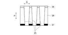
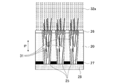
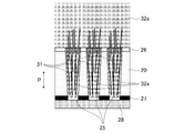
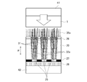
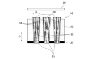
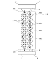
- FIG. 2 is a cross-sectional view taken along line AA of FIG. 1 in the anisotropic conductive sheet according to the same embodiment. It is an expanded sectional view of the electroconductive part in the anisotropically conductive sheet which concerns on the same embodiment. It is sectional drawing which shows the manufacturing process of the anisotropically conductive sheet which concerns on the same embodiment. It is sectional drawing which shows the manufacturing process of the anisotropically conductive sheet which concerns on the same embodiment. It is sectional drawing which shows the manufacturing process of the anisotropically conductive sheet which concerns on the same embodiment. It is sectional drawing which shows the manufacturing process of the anisotropically conductive sheet which concerns on the same embodiment.
- An anisotropic conductive sheet 10 accommodates an IC package 1 as an “electrical component” as shown in FIG.
- the sheet main body 20 has a plurality of conductive portions 30.
- the IC package 1 of this embodiment is a so-called BGA, has a package body 2 formed in a substantially square shape in plan view, and has a plurality of hemispherical terminals 3. Is formed so as to protrude downward on the lower surface of the package body 2.
- the substrate 6 of this embodiment has a substantially flat contact 8 at a position corresponding to the terminal 3 of the IC package 1 in the substrate body 7.
- the shape of the terminal 3 is not limited to a hemispherical shape, and may be an appropriate shape such as a substantially flat plate shape.
- the shape of the contact 8 is not limited to a substantially flat plate shape, and may be another shape.
- the sheet body 20 is made of a material having insulation properties and flexibility (here, silicone rubber), and is formed in a substantially rectangular thin plate shape. Further, the substantially central portion of the one surface side 21 of the sheet main body 20 is a housing portion 23 that houses the IC package 1 (see FIG. 13) to be tested. A plurality of conductive portions 30 are formed at a position corresponding to a square frame-shaped portion in the IC package 1.
- a substrate 6 (see FIG. 13) is arranged at a substantially central portion on the other surface side 22 opposite to the one surface side 21 of the sheet main body 20.
- the seat body 20 has a plurality of hole portions 25 penetrating the one surface side 21 and the other surface side 22 at a predetermined position of the accommodating portion 23.
- a plurality of conductive fibrous members 31 to be described later are placed, and a conductive portion 30 penetrating the one surface side 21 and the other surface side 22 of the sheet body 20 is formed.
- the conductive portion 30 is inserted into the hole 25 so that a plurality of substantially linear conductive fiber members 31 made of a predetermined conductive material such as nickel are in contact with each other. While the conductive fibrous members 31 are in contact with each other, they are held by a resin 32 (for example, a silicone resin) as a member having elasticity.
- a resin 32 for example, a silicone resin
- the length R in the longitudinal direction Q of the conductive fibrous member 31 is about 0.2 mm
- the wire diameter is about 20 ⁇ m
- the diameter S of the hole 25 is about 0.17 mm.
- the conductive fibrous member 31 is inserted in the hole 25 so that the longitudinal direction Q thereof faces in the substantially same direction as the penetration direction P on the one surface side 21 and the other surface side 22 of the sheet main body 20.
- the conductive fibrous members 31 placed in the holes 25 are configured to contact each other.
- the resin 32 is made of silicone resin or the like and has an elastic force
- the sheet body 20 is made of silicone rubber or the like and has an elastic force
- the conductive fibrous member 31 bends following the elastic deformation of these silicone rubbers.
- the conductive portion 30 is configured to have an elastic force with respect to the penetration direction P, and is configured to undergo predetermined elastic deformation with respect to the pressure with respect to the penetration direction P.
- the length R in the longitudinal direction Q of the conductive fibrous member 31 is formed to be longer than the diameter S of the hole 25 of the sheet main body 20.
- the manufacturing method of the anisotropic conductive sheet 10 is the same as the conventional manufacturing method except for the process of forming the conductive portion 30 described below, the description thereof is omitted.
- a resin film 26 such as PET is pasted on one side 21 (here, the upper surface side) of the sheet body 20 made of an elastic resin such as silicone, and the other side 22 (here, here).
- a resin film 27 such as polyimide is attached to the lower surface side, and a hole 25 penetrating from the one surface side 21 to the other surface side 22 is provided at a predetermined position by laser processing or the like.
- the hole 25 is formed so that the mouth on the one surface side 21 that is the upper surface side is wide and the mouth on the other surface side 22 that is the lower surface side is narrow, and thus the conductive fibrous member 31 can be easily inserted.
- the conductive fibrous member 31 is less likely to face sideways below the hole 25.
- the sheet main body 20 in the state of FIG. 4 is arranged and fixed on an adhesive sheet 28 made of polyimide, PET, polyethylene or the like, and the conductive fibrous member 31 is opened from the one side 21. Pour into part 25.
- the conductive fibrous member 31 is completely laid down in the hole 25. However, it is inserted into the hole 25 in an oblique state having at least a certain angle.
- the liquid silicone 32a contained in the container is arranged on the one surface side 21 of the sheet main body 20, and the silicone 32a is poured into the hole 25 as shown in FIG.
- the liquid silicone 32a is pressurized from above the container of the liquid silicone 32a with a pressing jig T or the like and cured in this state.
- magnetic force generators 41 and 42 such as electromagnets are provided above the pressing jig T and the adhesive sheet 28, respectively, and penetrated until the pressurized liquid silicone 32a is completely cured.
- the longitudinal direction Q of the plurality of conductive fibrous members 31 covered with the liquid silicone 32a in the hole 25 is changed from the state of FIG. 11 to the state of FIG.
- the conductive fibrous members 31 are aligned with each other in the penetrating direction P, and the conductive fibrous members 31 adhere to each other due to the magnetic force.
- the conductive state between the conductive fibrous members 31 becomes better, and it is possible to conduct from the one surface side 21 to the other surface side 22 with a small number of contacts Z.
- the drawing is extremely along the penetration direction P.
- the longitudinal direction Q of the conductive fibrous member 31 does not necessarily go to the penetrating direction P, and the longitudinal direction Q of the conductive fibrous member 31 may be substantially in the same direction as the penetrating direction P. .
- the silicone 32a when the silicone 32a is cured, as shown in FIG. 9, the excess silicone 32a at the top is cut out with a predetermined jig, and as shown in FIG.
- the anisotropic conductive sheet 10 formed with the plurality of conductive portions 30 composed of the members 31 is removed from the adhesive sheet 28 and the resin film 26 on the one surface side 21 of the sheet main body 20 is peeled off. Thereby, the contact Z of the conductive fibrous members 31 is small, the electrical resistance between the one surface side 21 and the other surface side 22 in the conductive portion 30 can be kept low, and the conductive portion having an elastic force with respect to the penetration direction P The anisotropic conductive sheet 10 in which 30 is formed can be obtained.
- the anisotropic conductive sheet 10 is disposed at a predetermined position on the substrate 6.
- the conductive portion 30 on the other surface side 22 of the sheet main body 20 of the anisotropic conductive sheet 10 is arranged so as to just contact the contact 8 provided from the substrate main body 7 of the substrate 6 toward the upper part. Set up.
- the IC package 1 is disposed at a predetermined position of the anisotropic conductive sheet 10.
- the terminals 3 provided downward from the package body 2 are arranged so as to be in contact with the conductive portion 30 in the accommodating portion 23 on the one surface side 21 of the sheet main body 20 of the anisotropic conductive sheet 10.
- the IC package 1 and the substrate 6 are brought into conduction through the anisotropic conductive sheet 10.
- the longitudinal direction Q of the plurality of conductive fibrous members 31 is The one surface side 21 and the other surface side 22 face substantially the same direction as the penetration direction P, and the plurality of conductive fibrous members 31 are in contact with each other.
- the contact Z between the conductive fibrous members 31 is very small compared to the number of contacts Z between the metal particles 131 of the conductive portion 130 clogged with the conventional metal particles 131 shown in FIG.
- the one surface side 21 and the other surface side 22 can be made conductive with each other in a small amount.
- the electrical resistance at the contact Z can be kept small.
- each of the plurality of conductive portions 30 includes the plurality of conductive fibrous members 31, and the plurality of conductive fibrous members 31 of the conductive portion 30 are included.
- the longitudinal direction Q of each conductive fibrous member 31 is substantially in the same direction as the penetration direction P between the one surface side 21 and the other surface side 22 of the sheet main body 20 and the conductive fibrous members 31 are in contact with each other and from the one surface side 21 to the other. Since the conductive state is formed toward the surface side 22, it is possible to reduce the number of contacts between the conductive fibrous members 31 when the one surface side 21 and the other surface side 22 are electrically connected, and from the one surface side 21 to the other side. The path when conducting to the surface side 22 can be straightened and shortened. As a result, the electrical resistance between the one surface side 21 and the other surface side 22 in the conductive portion 30 can be kept low.
- the anisotropic conductive sheet 10 of this embodiment has a plurality of conductive fibrous members 31 in each of a plurality of hole portions 25 provided in the sheet body 20, the conductive portion 30 is formed. With a simple configuration, it is possible to provide the conductive portion 30 with low electrical resistance.
- the conductive fibrous member 31 is a hole. It is possible to prevent a problem in which the longitudinal direction Q of the conductive fibrous member 31 does not face the penetrating direction P of the hole 25 because it lies sideways in the portion 25. As a result, the longitudinal direction Q of the conductive fibrous member 31 is surely directed to the penetration direction P of the hole 25, and the contact points between the conductive members between the one surface side 21 and the other surface side 22 can be suppressed to be small. And the path
- the anisotropic conductive sheet 10 of this embodiment is held by a plurality of conductive fibrous members 31 that are in contact with each other being hardened by a resin 32 having an elastic force, and an elastic force with respect to the penetration direction P. Since the conductive part 30 is formed by forming an elastic body having the above structure, the contact pressure between the conductive part 30 and the IC package 1 or the substrate 6 can be ensured.
- the manufacturing method of the anisotropically conductive sheet 10 of this embodiment is the penetration direction of the one surface side 21 and the other surface side 22 in the sheet body 20 in a state in which the plurality of conductive fibrous members 31 are embedded in the sheet body 20.
- the conductive fibrous members 31 are likely to follow along the lines of magnetic force due to the magnetic force, and the conductive fibrous members 31 are easily adhered to each other by the magnetic force. Is.
- the IC package 1 is used as the electrical component.
- the present invention is not limited to this, and the electrical component may be used for other electrical components other than the IC package.
- a plurality of the conductive fibrous members 31 are caused to follow the penetration direction P by continuously applying a magnetic force in the penetration direction P, and the conductive fibrous shape.
- the members 31 are attached to each other, but the present invention is not limited to this, and depending on conditions such as the amount, shape, size, and environment in the manufacturing process of the conductive fibrous member 31, good contact can be achieved without applying a magnetic force. In some cases, the conductive portion 30 in a state can be obtained.
- the conductive fibrous member 31 is inserted into the hole 25 formed in the sheet main body 20 to form the conductive portion 30, but the present invention is not limited to this.
- the sheet body does not have a hole portion and forms a sheet body formed of liquid silicone or the like
- the magnetic field is continuously applied to the portion where the conductive portion is formed, and the conductive fibrous member is put there.
- the conductive portion may be formed by collecting and curing the conductive fibrous member at the position of the conductive portion by magnetic force. At this time, by applying a magnetic force in the penetration direction from the one surface side to the other surface side of the sheet body, the conductive fibrous member can be directed in the direction along the penetration direction as in the above-described embodiment. It is.
- each member including the conductive fibrous member 31 and the conductive portion 30 in the above-described embodiment are not limited to this, and may be appropriately determined according to each condition. It ’s good.
- a plurality of conductive portions 30 ⁇ / b> A provided in the hole portions 25 formed in the sheet main body 20 are inserted into the hole portions 25.
- a fiber in which the conductive fibrous members 31A are hardened and held by a resin 32 having elasticity in a state where the conductive fibrous members 31A are in contact with each other, and the plurality of conductive fibrous members 31A are nickel-plated on wave-shaped acrylic fibers The case where it is comprised with a shaped member is mentioned.
- the conductive fibrous member 31 ⁇ / b> A has a size and a shape such that the longitudinal direction thereof is substantially in the same direction as the penetration direction P of the hole 25.
- a plurality of conductive portions 30B provided in a plurality of hole portions 25 formed in the sheet body 20 are provided in the plurality of hole portions 25.
- the conductive fibrous members 31B are hardened and held by an elastic resin 32 in contact with each other, and the plurality of conductive fibrous members 31B apply nickel plating to a spring having a predetermined length. The case where it is comprised by the spiral-shaped fibrous member which was made is mentioned.
- the conductive fibrous member 31 ⁇ / b> B has a size and a shape such that the axial direction of the spiral shape faces substantially the same direction as the penetration direction P of the hole 25.
- a plurality of conductive portions 30 ⁇ / b> C provided in the hole portions 25 formed in the sheet main body 20 are provided in the hole portions 25.
- the conductive fibrous members 31C are fixed and held by an elastic resin 32 in a state where the conductive fibrous members 31C are in contact with each other. The case where it is comprised with the annular-shaped fibrous member which gave plating is mentioned.
- the diameter direction of the annular shape faces substantially the same direction as the penetration direction P of the hole 25 (the direction in which the center axis direction of the annular shape is substantially orthogonal to the penetration direction P of the hole 25). Size and shape).
Landscapes
- Engineering & Computer Science (AREA)
- Manufacturing & Machinery (AREA)
- Non-Insulated Conductors (AREA)
- Manufacturing Of Electrical Connectors (AREA)
- Testing Of Individual Semiconductor Devices (AREA)
Abstract
簡単な構造で、導電部における一面側から他面側までの間の電気抵抗を低く抑えることができる異方導電性シート及びその製造方法を提供することを課題とする。絶縁性を有する材質からなるシート本体(20)と、シート本体(20)の一面側(21)と他面側(22)を貫通するように設けられ、導電性を有する材質からなる複数の導電部(30)と、を有する異方導電性シート(10)である。複数の導電部(30)はそれぞれ、複数の導電繊維状部材(31)を有している。導電部(30)の複数の導電繊維状部材(31)は、各導電繊維状部材(31)の長手方向(Q)が一面側(21)と他面側(22)の貫通方向(P)と略同方向に沿い、かつ、導電繊維状部材(31)同士が接触して一面側(21)から他面側(22)に向かって導通状態を形成している。
Description
この発明は、半導体装置(以下「ICパッケージ」という)等の電気部品の試験等に使用する異方導電性シート及びその製造方法に関するものである。
従来、「電気部品」であるICパッケージの試験等において、当該ICパッケージを収容して、配線基板等に導通させる異方導電性シートがある。
そのような異方導電性シートにおいては、絶縁性を有するシート本体に導電性を有する導電部が複数設けられているが、この導電部はそれぞれ、複数の金属粒子で構成されているものが多かった(特許文献1参照)。
しかしながら、従来のものにあっては、前記した特許文献1の構成を概念的に示した図14のように、異方導電性シート110のシート本体120に対して設けられる導電部130が複数の金属粒子131で構成されているため、導電部130においてICパッケージ1の端子3が接触するシート本体20の一面側121と基板6の接触子8が接触するシート本体20の他面側122が導通するまでの間に金属粒子131同士の接点Zを多く通過する必要があった。その結果、電気抵抗が高くなってしまうという問題が生じていた。
そこで、この発明は、簡単な構造で、導電部における一面側から他面側までの間の電気抵抗を低く抑えることができる異方導電性シート及びその製造方法を提供することを課題としている。
かかる課題を達成するために、請求項1に記載の発明は、絶縁性を有する材質からなるシート本体と、該シート本体の一面側と他面側を貫通するように設けられ、導電性を有する材質からなる複数の導電部と、を有する異方導電性シートであって、複数の前記導電部はそれぞれ、複数の導電繊維状部材を有しており、前記導電部の複数の前記導電繊維状部材は、各導電繊維状部材の長手方向が前記一面側と前記他面側の貫通方向と略同方向に沿い、かつ、前記導電繊維状部材同士が接触して前記一面側から他面側に向かって導通状態を形成している異方導電性シートとしたことを特徴とする。
また、請求項2に記載の発明は、請求項1に記載の発明に加えて、前記シート本体には、前記一面側から前記他面側に貫通する複数の孔部が設けられており、該孔部に前記導電部が設けられている異方導電性シートとしたことを特徴とする。
また、請求項3に記載の発明は、請求項2に記載の発明に加えて、前記導電繊維状部材は、それぞれの前記長手方向の長さが、前記孔部の径より長く形成されている異方導電性シートとしたことを特徴とする。
また、請求項4に記載の発明は、請求項1乃至3の何れか一つに記載の発明に加えて、前記導電部は、互いに接触した複数の前記導電繊維状部材が、弾性力を有する部材で保持されて、弾性体を構成しており、前記貫通方向に対して弾性力を有している異方導電性シートとしたことを特徴とする。
また、請求項5に記載の発明は、請求項1乃至3の何れか一つに記載の異方導電性シートの製造方法であって、絶縁性を有する材質からなるシート本体に対して、該シート本体の一面側と他面側を貫通する複数の導電部となる箇所の液状の部分それぞれに複数の導電繊維状部材を埋め込んだ上で、前記一面側と前記他面側の貫通方向に磁力を掛けることで、当該磁力により複数の前記導電繊維状部材の長手方向が前記貫通方向を向くようにし、かつ、当該磁力により複数の前記導電繊維状部材同士を接触させ、前記液状の部分を硬化させる異方導電性シートの製造方法としたことを特徴とする。
請求項1に記載の発明によれば、異方導電性シートにおける複数の導電部がそれぞれ、複数の導電繊維状部材を有しており、導電部の複数の導電繊維状部材が、各導電繊維状部材の長手方向がシートの一面側と他面側の貫通方向と略同方向に沿うと共に導電繊維状部材同士が接触して一面側から他面側に向かって導通状態を形成しているため、一面側と他面側を導通させる際の導電繊維状部材同士の接点を少なく抑えることができる。その結果、導電部における一面側から他面側までの間の電気抵抗を低く抑えることができる。
請求項2に記載の発明によれば、シート本体に設けられた複数の孔部それぞれに複数の導電繊維状部材が入れられて導電部が形成されているため、簡単な構成で、電気抵抗を低く抑えた導電部を設けることができる。
請求項3に記載の発明によれば、導電繊維状部材の長手方向の長さが孔部の径より長く形成されているため、導電繊維状部材が孔部の中で横倒しになって、導電繊維状部材の長手方向が孔部の貫通方向を向かなくなってしまう不具合を防止することができる。その結果、確実に、導電繊維状部材の長手方向が孔部の貫通方向を向いて、一面側と他面側の間の導電部材同士の接点を少なく抑えることができる。
請求項4に記載の発明によれば、互いに接触した複数の導電繊維状部材が、弾性力を有する部材で保持されて、貫通方向に対して弾性力を有する弾性体を形成して、導電部を構成しているため、導電部と電気部品や基板との接圧を確保することができる。
請求項5に記載の発明によれば、異方導電性シートの製造方法において、シート本体に複数の導電繊維状部材を埋め込んだ状態で、シート本体における一面側と他面側の貫通方向に磁力を掛けることで、当該磁力によって磁力線上に導電繊維状部材が沿い易くなり、かつ、導電繊維状部材同士が磁力によって密着し易くなるため、導通部の成形がし易くなるものである。
以下、この発明の実施の形態について説明する。
図1~図13には、この発明の実施の形態を示す。
まず構成を説明すると、この実施の形態に係る異方導電性シート10は、図13に示すように、「電気部品」としてのICパッケージ1を収容して、基板6上に配設して試験等を行うためのものであり、図1及び図2に示すように、シート本体20に複数の導電部30を有する構成となっている。
まず、ICパッケージ1と基板6について説明する。図13に示すように、この実施の形態のICパッケージ1は、所謂BGAと称されるもので、平面視で略正方形状に形成されたパッケージ本体2を有し、複数の半球状の端子3がこのパッケージ本体2の下面に下向きに突出して形成されたものである。また、この実施の形態の基板6は、その基板本体7における、ICパッケージ1の端子3に対応する位置に、略平板状の接触子8を有している。なお、端子3の形状は、半球状に限るものではなく、略平板状等の適宜の形状であっても良い。また、接触子8の形状も、略平板状に限るものではなく、他の形状であっても良い。
また、異方導電性シート10のうち、シート本体20は、絶縁性を有すると共に可撓性を有する材質(ここではシリコーンゴム)で構成されており、略方形の薄板状に形成されている。また、シート本体20の一面側21の略中央部は、試験対象であるICパッケージ1(図13参照)を収容する収容部23となっており、当該収容部23の所定位置(ここでは収容したICパッケージ1における四角枠状の部分に相当する位置)には、複数の導電部30が形成されている。
また、シート本体20の一面側21とは反対の他面側22の略中央部には、基板6(図13参照)が配置されるようになっている。また、シート本体20における前記した収容部23の所定位置には、図3に示すように、一面側21と他面側22を貫通する複数の孔部25を有しており、この孔部25に、後述する複数の導電繊維状部材31が入れられて、シート本体20の一面側21と他面側22を貫通する導電部30が形成されている。
以下、導電部30について詳述する。この導電部30は、図3に示すように、ニッケル等の所定の導電性材料からなる複数の略直線形状の導電繊維状部材31が互いに接触するように孔部25に入れられており、当該導電繊維状部材31が互いに接触した状態で、弾性力を有する部材としての樹脂32(例えばシリコーン樹脂等)で保持されている。ここでは、導電繊維状部材31の長手方向Qの長さRは約0.2mm、線径は約20μmであり、孔部25の径Sは約0.17mmに形成されている。また、導電繊維状部材31は、その長手方向Qがシート本体20の一面側21と他面側22の貫通方向Pと略同方向に向くように孔部25に入れられており、当該状態で、当該孔部25に入れられた導電繊維状部材31同士が接触し合うように構成されている。
また、樹脂32がシリコーン樹脂等で弾性力を有することと、シート本体20がシリコーンゴム等で弾性力を有することにより、これらのシリコーンゴムの弾性変形に追随して導電繊維状部材31が湾曲して、導電部30は貫通方向Pに対して弾性力を有するように構成されており、貫通方向Pに対する圧力に対して、所定の弾性変形をするように構成されている。
また、前記したように、導電繊維状部材31の長手方向Qの長さRは、シート本体20の孔部25の径Sより長くなるように形成されている。これにより、導電繊維状部材31を孔部25に入れ込んだときに、孔部25の中で完全に横倒しにはならず、少なくとも一定の角度を持って斜めに挿入された状態に配置されるようになっている。
次に、この実施の形態に係る異方導電性シート10の製造方法について、図4~図12を用いて説明する。なお、異方導電性シート10の製造方法のうち、以下で説明する導電部30の形成工程以外は、従来の製造方法と変わらないため、説明を省略する。
まず、図4に示すように、シリコーン等の弾性力を有する樹脂からなるシート本体20の一面側21(ここでは上面側)にPET等の樹脂フィルム26を貼り付け、他面側22(ここでは下面側)にポリイミド等の樹脂フィルム27を貼り付け、レーザ加工等によって予め定められた所定位置に一面側21から他面側22に貫通する孔部25を設ける。このとき、孔部25を、上面側である一面側21の口が広く下面側である他面側22の口が狭くなるように形成しており、これにより、導電繊維状部材31を入れ易く、また、孔部25の下方で導電繊維状部材31が横向きになり難くなっている。
次に、図5に示すように、図4の状態のシート本体20をポリイミド、PET、ポリエチレン等からなる粘着シート28の上に配置して固定し、導電繊維状部材31を一面側21から孔部25に流し入れる。このとき、導電繊維状部材31の長手方向Qの長さRは、孔部25の径Sより長くなるように形成されているため、孔部25の中で導電繊維状部材31が完全に横倒しになることはなく、少なくとも一定角度を有する斜め状態で孔部25に挿入された状態となる。
次に、図6に示すように、容器に入れられた液状シリコーン32aをシート本体20の一面側21に配置し、図7に示すように、当該シリコーン32aを孔部25に流し込む。
次に、図8に示すように、液状シリコーン32aの容器の上方から加圧用治具T等によって液状シリコーン32aを加圧し、当該状態で硬化させる。
このとき、図12に示すように、加圧用治具Tの上方と粘着シート28にそれぞれ電磁石等の磁力発生装置41,42を備えていて、加圧された液状シリコーン32aが硬化し終わるまで貫通方向Pに磁力が掛かるようにし続けることにより、図11の状態から図12の状態のように、孔部25の中の液状シリコーン32aに覆われた複数の導電繊維状部材31の長手方向Qが、より貫通方向Pに向かって整列するようになり、それと共に磁力により導電繊維状部材31同士がくっつき合うようになる。
これにより、より導電繊維状部材31同士の導通状態が良好となり、かつ、少ない接点Zで一面側21から他面側22に導通されるようにできる。なお、図12では、磁力を掛けたときに導電繊維状部材31の長手方向Qが貫通方向Pに向く様子を分かり易く説明するために、極端に貫通方向Pに沿った図となっているが、必ずしもここまで極端に導電繊維状部材31の長手方向Qが貫通方向Pに向かうとは限らず、導電繊維状部材31の長手方向Qが貫通方向Pと略同方向に向かう程度の場合もある。
その後、シリコーン32aが硬化したら、図9に示すように、上部の余ったシリコーン32aを所定の治具で切り取り、図10に示すように、樹脂32で固められて保持された複数の導電繊維状部材31で構成された複数の導電部30が形成された異方導電性シート10を、粘着シート28から取り外すと共に、シート本体20の一面側21の樹脂フィルム26を剥離する。これにより、導電繊維状部材31同士の接点Zが少なく、導電部30における一面側21から他面側22までの間の電気抵抗を低く抑えることができ、貫通方向Pに対する弾性力を有する導電部30が形成された異方導電性シート10を得ることができる。
次に、この実施の形態の異方導電性シート10を用いてICパッケージ1の試験を行うときの作用について、図13及び図14を用いて説明する。
まず、異方導電性シート10を基板6の所定位置に配設する。ここでは、基板6の基板本体7から上部に向けて設けられた接触子8に対して、異方導電性シート10のシート本体20の他面側22の導電部30が丁度当接するように配設する。
次に、ICパッケージ1を異方導電性シート10の所定位置に配置する。ここでは、パッケージ本体2から下部に向けて設けられた端子3を異方導電性シート10のシート本体20の一面側21の収容部23における導電部30に丁度当接させるように配置する。これにより、異方導電性シート10を介してICパッケージ1と基板6が導通状態となる。
次に、設定された所定条件にて、電気を導通させる。このとき、異方導電性シート10の一面側21に収容されたICパッケージ1と他面側に設けられた基板6の間の導電部30において、複数の導電繊維状部材31の長手方向Qが一面側21と他面側22の貫通方向Pと略同方向を向くようになっており、かつ、複数の導電繊維状部材31同士が接触し合った状態となっている。
これにより、図14に示す従来の金属粒子131が詰まった導電部130の金属粒子131同士の接点Zの数に比べて、図13に示すように、導電繊維状部材31同士の接点Zが非常に少ない状態で、一面側21と他面側22を導通させることができる。接点Zが少なくなった結果、当該接点Zにおける電気抵抗を小さく抑えることができる。
このように、この実施の形態の異方導電性シート10は、複数の導電部30がそれぞれ、複数の導電繊維状部材31を有しており、導電部30の複数の導電繊維状部材31が、各導電繊維状部材31の長手方向Qがシート本体20の一面側21と他面側22の貫通方向Pと略同方向に沿うと共に導電繊維状部材31同士が接触して一面側21から他面側22に向かって導通状態を形成しているため、一面側21と他面側22を導通させる際の導電繊維状部材31同士の接点を少なく抑えることができ、かつ、一面側21から他面側22に導通するときの経路を直線的にして短くすることができる。その結果、導電部30における一面側21から他面側22までの間の電気抵抗を低く抑えることができる。
また、この実施の形態の異方導電性シート10は、シート本体20に設けられた複数の孔部25それぞれに複数の導電繊維状部材31が入れられて導電部30が形成されているため、簡単な構成で、電気抵抗を低く抑えた導電部30を設けることができる。
また、この実施の形態の異方導電性シート10は、導電繊維状部材31の長手方向Qの長さRが孔部25の径Sより長く形成されているため、導電繊維状部材31が孔部25の中で横倒しになって、導電繊維状部材31の長手方向Qが孔部25の貫通方向Pを向かなくなってしまう不具合を防止することができる。その結果、確実に、導電繊維状部材31の長手方向Qが孔部25の貫通方向Pを向いて、一面側21と他面側22の間の導電部材同士の接点を少なく抑えることができ、かつ、一面側21から他面側22に導通するときの経路を直線的にして短くすることができる。
また、この実施の形態の異方導電性シート10は、互いに接触した複数の導電繊維状部材31が、弾性力を有する樹脂32で固められることで保持されて、貫通方向Pに対して弾性力を有する弾性体を形成して、導電部30を構成しているため、導電部30とICパッケージ1や基板6との接圧を確保することができる。
また、この実施の形態の異方導電性シート10の製造方法は、シート本体20に複数の導電繊維状部材31を埋め込んだ状態で、シート本体20における一面側21と他面側22の貫通方向Pに磁力を掛けることで、当該磁力によって磁力線上に導電繊維状部材31が沿い易くなり、かつ、導電繊維状部材31同士が磁力によって密着し易くなるため、導通部30の成形がし易くなるものである。
なお、前記した実施の形態では、電気部品としてICパッケージ1を用いて説明したが、これに限るものではなく、ICパッケージ以外の他の電気部品に用いられるようになっていても良い。
また、前記した実施の形態では、異方導電性シート10の製造過程において、貫通方向Pに磁力を掛け続けて複数の導電繊維状部材31を貫通方向Pに沿うようにさせると共に、導電繊維状部材31同士をくっつけ合うようにしたが、これに限るものではなく、導電繊維状部材31の量や形状、大きさ、製造過程における環境等の条件によっては、磁力を掛けなくても良好な接触状態の導電部30が得られる場合もある。
また、前記した実施の形態では、シート本体20に形成された孔部25に導電繊維状部材31を入れ込んで導電部30を形成するようになっていたが、これに限るものではない。例えば、シート本体に孔部を有しておらず、液状のシリコーン等で形成されたシート本体を形成するものの、導電部が形成される箇所に磁力をかけ続け、そこに導電繊維状部材を入れることで、磁力によって導電部の箇所に導電繊維状部材を集めて硬化させることで、導電部を形成するようになっていても良い。なお、このとき、磁力をシート本体の一面側から他面側への貫通方向に掛けておくことで、前記した実施の形態のように導電繊維状部材を貫通方向沿う方向に向けることができるものである。
また、前記した実施の形態における導電繊維状部材31や導電部30を含む各部材の材質や形状、大きさ等は、これに限るものではなく、それぞれの条件等に応じて、適宜決定すれば良いものである。
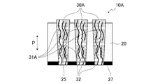
例えば、図15に示す第1変形の異方導電性シート10Aのように、シート本体20に複数形成された孔部25に設けられた導電部30Aが、当該孔部25に入れられた複数の導電繊維状部材31Aが互いに接触した状態で弾性力を有する樹脂32で固められて保持されたものであって、複数の導電繊維状部材31Aが、波形状のアクリル繊維にニッケルメッキを施した繊維状部材で構成されている場合が挙げられる。この導電繊維状部材31Aは、その長手方向が孔部25の貫通方向Pと略同方向を向くような大きさ及び形状となっている。
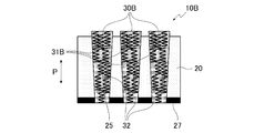
また、図16に示す第2変形の異方導電性シート10Bのように、シート本体20に複数形成された孔部25に設けられた導電部30Bが、当該孔部25に入れられた複数の導電繊維状部材31Bが互いに接触した状態で弾性力を有する樹脂32で固められて保持されたものであって、複数の導電繊維状部材31Bが、所定の長さを有するスプリングにニッケルメッキを施した螺旋形状の繊維状部材で構成されている場合が挙げられる。この導電繊維状部材31Bは、その螺旋形状の軸方向が孔部25の貫通方向Pと略同方向を向くような大きさ及び形状となっている。
また、図17に示す第3変形の異方導電性シート10Cのように、シート本体20に複数形成された孔部25に設けられた導電部30Cが、当該孔部25に入れられた複数の導電繊維状部材31Cが互いに接触した状態で弾性力を有する樹脂32で固められて保持されたものであって、複数の導電繊維状部材31Cが、所定の大きさの一巻状のスプリングにニッケルメッキを施した円環形状の繊維状部材で構成されている場合が挙げられる。この導電繊維状部材31Cは、その円環形状の直径方向が孔部25の貫通方向Pと略同方向を向く(円環形状の中心軸方向が孔部25の貫通方向Pと略直交する方向を向く)ような大きさ及び形状となっている。
10 異方導電性シート
20 シート本体
21 一面側
22 他面側
25 孔部
30 導電部
31 導電繊維状部材
32 樹脂
41 磁力体
42 磁力体
P 貫通方向
Q 長手方向
R 導電繊維状部材の長手方向の長さ
S 孔部の径
Z 接点
20 シート本体
21 一面側
22 他面側
25 孔部
30 導電部
31 導電繊維状部材
32 樹脂
41 磁力体
42 磁力体
P 貫通方向
Q 長手方向
R 導電繊維状部材の長手方向の長さ
S 孔部の径
Z 接点
Claims (5)
- 絶縁性を有する材質からなるシート本体と、
該シート本体の一面側と他面側を貫通するように設けられ、導電性を有する材質からなる複数の導電部と、
を有する異方導電性シートであって、
複数の前記導電部はそれぞれ、複数の導電繊維状部材を有しており、
前記導電部の複数の前記導電繊維状部材は、各導電繊維状部材の長手方向が前記一面側と前記他面側の貫通方向と略同方向に沿い、かつ、前記導電繊維状部材同士が接触して前記一面側から他面側に向かって導通状態を形成していることを特徴とする異方導電性シート。 - 前記シート本体には、前記一面側から前記他面側に貫通する複数の孔部が設けられており、
該孔部に前記導電部が設けられていることを特徴とする請求項1に記載の異方導電性シート。 - 前記導電繊維状部材は、それぞれの前記長手方向の長さが、前記孔部の径より長く形成されていることを特徴とする請求項2に記載の異方導電性シート。
- 前記導電部は、互いに接触した複数の前記導電繊維状部材が、弾性力を有する部材で保持されて、弾性体を構成しており、前記貫通方向に対して弾性力を有していることを特徴とする請求項1乃至3の何れか一つに記載の異方導電性シート。
- 請求項1乃至3の何れか一つに記載の異方導電性シートの製造方法であって、
絶縁性を有する材質からなるシート本体に対して、該シート本体の一面側と他面側を貫通する複数の導電部となる箇所の液状の部分それぞれに複数の導電繊維状部材を埋め込んだ上で、前記一面側と前記他面側の貫通方向に磁力を掛けることで、当該磁力により複数の前記導電繊維状部材の長手方向が前記貫通方向を向くようにし、かつ、当該磁力により複数の前記導電繊維状部材同士を接触させ、前記液状の部分を硬化させることを特徴とする異方導電性シートの製造方法。
Priority Applications (1)
| Application Number | Priority Date | Filing Date | Title |
|---|---|---|---|
| US16/341,308 US10720398B2 (en) | 2016-10-27 | 2017-10-26 | Anisotropic conductive sheet and method for manufacturing the same |
Applications Claiming Priority (2)
| Application Number | Priority Date | Filing Date | Title |
|---|---|---|---|
| JP2016-210695 | 2016-10-27 | ||
| JP2016210695A JP2018073577A (ja) | 2016-10-27 | 2016-10-27 | 異方導電性シート及びその製造方法 |
Publications (1)
| Publication Number | Publication Date |
|---|---|
| WO2018079655A1 true WO2018079655A1 (ja) | 2018-05-03 |
Family
ID=62023654
Family Applications (1)
| Application Number | Title | Priority Date | Filing Date |
|---|---|---|---|
| PCT/JP2017/038704 Ceased WO2018079655A1 (ja) | 2016-10-27 | 2017-10-26 | 異方導電性シート及びその製造方法 |
Country Status (4)
| Country | Link |
|---|---|
| US (1) | US10720398B2 (ja) |
| JP (1) | JP2018073577A (ja) |
| TW (1) | TW201830779A (ja) |
| WO (1) | WO2018079655A1 (ja) |
Cited By (1)
| Publication number | Priority date | Publication date | Assignee | Title |
|---|---|---|---|---|
| WO2019244948A1 (ja) * | 2018-06-19 | 2019-12-26 | 積水ポリマテック株式会社 | 導電ゴムコネクタ及び導電ゴムコネクタの製造方法 |
Families Citing this family (1)
| Publication number | Priority date | Publication date | Assignee | Title |
|---|---|---|---|---|
| CN117546370A (zh) * | 2021-07-28 | 2024-02-09 | 弗劳恩霍夫应用研究促进协会 | 接触装置、接触装置制造方法及组件 |
Citations (6)
| Publication number | Priority date | Publication date | Assignee | Title |
|---|---|---|---|---|
| JP2001322139A (ja) * | 2000-05-16 | 2001-11-20 | Jsr Corp | 複合シートの製造方法および複合シート |
| JP2003257542A (ja) * | 2002-03-05 | 2003-09-12 | Polymatech Co Ltd | 防爆コネクタ |
| JP3123971U (ja) * | 2006-05-22 | 2006-08-03 | 遠行科技股▲ふん▼有限公司 | 導電ゴムの構造 |
| JP2008058286A (ja) * | 2006-08-31 | 2008-03-13 | Shuichi Ikeda | 摺動型接触子 |
| JP2010043256A (ja) * | 2008-08-05 | 2010-02-25 | World Properties Inc | 導電性ポリマー発泡体、その作製方法、ならびにその物品およびその使用 |
| WO2011027692A1 (ja) * | 2009-09-02 | 2011-03-10 | ポリマテック株式会社 | 異方導電体及び異方導電体の製造方法並びに異方導電体配列シート |
Family Cites Families (52)
| Publication number | Priority date | Publication date | Assignee | Title |
|---|---|---|---|---|
| US4209481A (en) * | 1976-04-19 | 1980-06-24 | Toray Industries, Inc. | Process for producing an anisotropically electroconductive sheet |
| JP3038859B2 (ja) | 1989-09-29 | 2000-05-08 | ジェイエスアール株式会社 | 異方導電性シート |
| US5441690A (en) * | 1993-07-06 | 1995-08-15 | International Business Machines Corporation | Process of making pinless connector |
| US5385477A (en) * | 1993-07-30 | 1995-01-31 | Ck Technologies, Inc. | Contactor with elastomer encapsulated probes |
| DE69738128T2 (de) * | 1996-04-05 | 2008-06-05 | The University Of Virginia Patent Foundation | Metallfaserbürste mit permanentem kontakt |
| JPH1140224A (ja) * | 1997-07-11 | 1999-02-12 | Jsr Corp | 異方導電性シート |
| US6011307A (en) * | 1997-08-12 | 2000-01-04 | Micron Technology, Inc. | Anisotropic conductive interconnect material for electronic devices, method of use and resulting product |
| US6854985B1 (en) * | 1998-12-16 | 2005-02-15 | Paricon Technologies Corporation | Elastomeric interconnection device and methods for making same |
| TW561266B (en) * | 1999-09-17 | 2003-11-11 | Jsr Corp | Anisotropic conductive sheet, its manufacturing method, and connector |
| US6264476B1 (en) * | 1999-12-09 | 2001-07-24 | High Connection Density, Inc. | Wire segment based interposer for high frequency electrical connection |
| JP4240724B2 (ja) * | 2000-01-26 | 2009-03-18 | Jsr株式会社 | 異方導電性シートおよびコネクター |
| CN1230944C (zh) * | 2000-08-09 | 2005-12-07 | Jsr株式会社 | 各向异性导电板 |
| DE60107519T2 (de) * | 2000-09-25 | 2005-12-15 | Jsr Corp. | Anisotropisches leitfähiges Verbindungsblatt, Herstellungsverfahren dafür und Produkt davon |
| KR20030078870A (ko) * | 2000-12-08 | 2003-10-08 | 제이에스알 가부시끼가이샤 | 이방 도전성 시트 및 웨이퍼 검사 장치 |
| US6969622B1 (en) * | 2001-02-09 | 2005-11-29 | Jsr Corporation | Anisotropically conductive connector, its manufacture method and probe member |
| US6465084B1 (en) * | 2001-04-12 | 2002-10-15 | International Business Machines Corporation | Method and structure for producing Z-axis interconnection assembly of printed wiring board elements |
| US20030094666A1 (en) * | 2001-11-16 | 2003-05-22 | R-Tec Corporation | Interposer |
| US7160123B2 (en) * | 2002-03-07 | 2007-01-09 | Jsr Corporation | Plural layer anisotropic conductive connector and its production method |
| DE60314164T2 (de) * | 2002-08-09 | 2008-02-07 | Jsr Corp. | Prüfverbinder mit anisotroper leitfähigkeit |
| US7095241B2 (en) * | 2002-08-09 | 2006-08-22 | Jsr Corporation | Anisotropic conductive connector, probe member, wafer inspecting device, and wafer inspecting method |
| JP3685192B2 (ja) * | 2002-08-09 | 2005-08-17 | Jsr株式会社 | 異方導電性コネクターおよび導電性ペースト組成物、プローブ部材並びにウエハ検査装置およびウエハ検査方法 |
| US6712620B1 (en) * | 2002-09-12 | 2004-03-30 | High Connection Density, Inc. | Coaxial elastomeric connector system |
| ATE515078T1 (de) * | 2003-01-17 | 2011-07-15 | Jsr Corp | Anisotroper leitfähiger verbinder und herstellungsverfahren dafür und untersuchungseinheit für eine schaltungseinrichtung |
| JP2004265729A (ja) * | 2003-02-28 | 2004-09-24 | Jst Mfg Co Ltd | 異方導電シート |
| US7014479B2 (en) * | 2003-03-24 | 2006-03-21 | Che-Yu Li | Electrical contact and connector and method of manufacture |
| US7040902B2 (en) * | 2003-03-24 | 2006-05-09 | Che-Yu Li & Company, Llc | Electrical contact |
| US7029288B2 (en) * | 2003-03-24 | 2006-04-18 | Che-Yu Li | Electrical contact and connector and method of manufacture |
| EP1608040A4 (en) * | 2003-03-26 | 2007-11-14 | Jsr Corp | ANISOTROPER CONDUCTIVE CONNECTOR, CONDUCTIVE PASTE COMPOSITION, SONDER, WAFER INSPECTION DEVICE AND WAFER SEARCH METHOD |
| TWI239684B (en) * | 2003-04-16 | 2005-09-11 | Jsr Corp | Anisotropic conductive connector and electric inspection device for circuit device |
| EP1640729A4 (en) * | 2003-06-09 | 2010-06-16 | Jsr Corp | ANISOTROPIC CONDUCTIVE CONNECTOR AND WAFER INSPECTION DEVICE |
| WO2004112195A1 (ja) * | 2003-06-12 | 2004-12-23 | Jsr Corporation | 異方導電性コネクター装置およびその製造方法並びに回路装置の検査装置 |
| EP1686655A4 (en) * | 2003-11-17 | 2008-02-13 | Jsr Corp | Anisotropic conductive sheet, manufacturing method thereof, and product using the same |
| US20060177971A1 (en) * | 2004-01-13 | 2006-08-10 | Jsr Corporation | Anisotropically conductive connector, production process thereof and application product thereof |
| WO2006087877A1 (ja) * | 2005-02-16 | 2006-08-24 | Jsr Corporation | 複合導電性シートおよびその製造方法、異方導電性コネクター、アダプター装置並びに回路装置の電気的検査装置 |
| JP2006294527A (ja) * | 2005-04-14 | 2006-10-26 | Nec Corp | コネクタ及びその製造方法 |
| US20060280912A1 (en) * | 2005-06-13 | 2006-12-14 | Rong-Chang Liang | Non-random array anisotropic conductive film (ACF) and manufacturing processes |
| US7922497B2 (en) * | 2005-10-11 | 2011-04-12 | Jsr Corporation | Anisotropic conductive connector and inspection equipment of circuit device |
| US7402051B1 (en) * | 2005-11-10 | 2008-07-22 | Antares Advanced Test Technologies, Inc. | Interconnect assembly for testing integrated circuit packages |
| US7297004B1 (en) * | 2006-02-06 | 2007-11-20 | Antares Advanced Test Technologies, Inc. | Crimped tube electrical test socket pin |
| EP2015399A4 (en) * | 2006-04-11 | 2013-01-30 | Jsr Corp | ANISOTROPER CONDUCTIVE CONNECTOR AND ANISOTROPE CONDUCTIVE CONNECTOR ASSEMBLY |
| JP4825043B2 (ja) * | 2006-04-21 | 2011-11-30 | ポリマテック株式会社 | 異方導電性シート |
| US8093970B2 (en) * | 2007-10-12 | 2012-01-10 | Montara Technologies LLC | Braided electrical contact element based relay |
| CN101971037A (zh) * | 2008-03-14 | 2011-02-09 | 富士胶片株式会社 | 探针卡 |
| IT1395336B1 (it) * | 2009-01-20 | 2012-09-14 | Rise Technology S R L | Dispositivo di contatto elastico per componenti elettronici a colonne collassanti |
| WO2010101125A1 (ja) * | 2009-03-05 | 2010-09-10 | ポリマテック株式会社 | 弾性コネクタ及び弾性コネクタの製造方法並びに導通接続具 |
| US7833020B1 (en) * | 2009-06-15 | 2010-11-16 | Hon Hai Precision Ind. Co., Ltd. | Electrical connector with low profile terminal |
| FR2958407B1 (fr) * | 2010-04-02 | 2012-12-28 | Snecma | Procede d'analyse d'une pluralite de particules ferromagnetiques |
| US8870579B1 (en) * | 2011-01-14 | 2014-10-28 | Paricon Technologies Corporation | Thermally and electrically enhanced elastomeric conductive materials |
| WO2012132092A1 (ja) * | 2011-03-25 | 2012-10-04 | 富士高分子工業株式会社 | ワイヤ配列ゴムコネクタ及びその製造方法 |
| TWI462244B (zh) * | 2011-10-17 | 2014-11-21 | 財團法人工業技術研究院 | 異方向性導電膜片及其製作方法 |
| JP2015207433A (ja) * | 2014-04-18 | 2015-11-19 | 矢崎総業株式会社 | 導電性弾性部材及びコネクタ |
| WO2016068168A1 (ja) * | 2014-10-28 | 2016-05-06 | デクセリアルズ株式会社 | 異方性導電フィルム、その製造方法、及び接続構造体 |
-
2016
- 2016-10-27 JP JP2016210695A patent/JP2018073577A/ja active Pending
-
2017
- 2017-10-26 WO PCT/JP2017/038704 patent/WO2018079655A1/ja not_active Ceased
- 2017-10-26 US US16/341,308 patent/US10720398B2/en not_active Expired - Fee Related
- 2017-10-27 TW TW106137072A patent/TW201830779A/zh unknown
Patent Citations (6)
| Publication number | Priority date | Publication date | Assignee | Title |
|---|---|---|---|---|
| JP2001322139A (ja) * | 2000-05-16 | 2001-11-20 | Jsr Corp | 複合シートの製造方法および複合シート |
| JP2003257542A (ja) * | 2002-03-05 | 2003-09-12 | Polymatech Co Ltd | 防爆コネクタ |
| JP3123971U (ja) * | 2006-05-22 | 2006-08-03 | 遠行科技股▲ふん▼有限公司 | 導電ゴムの構造 |
| JP2008058286A (ja) * | 2006-08-31 | 2008-03-13 | Shuichi Ikeda | 摺動型接触子 |
| JP2010043256A (ja) * | 2008-08-05 | 2010-02-25 | World Properties Inc | 導電性ポリマー発泡体、その作製方法、ならびにその物品およびその使用 |
| WO2011027692A1 (ja) * | 2009-09-02 | 2011-03-10 | ポリマテック株式会社 | 異方導電体及び異方導電体の製造方法並びに異方導電体配列シート |
Cited By (1)
| Publication number | Priority date | Publication date | Assignee | Title |
|---|---|---|---|---|
| WO2019244948A1 (ja) * | 2018-06-19 | 2019-12-26 | 積水ポリマテック株式会社 | 導電ゴムコネクタ及び導電ゴムコネクタの製造方法 |
Also Published As
| Publication number | Publication date |
|---|---|
| JP2018073577A (ja) | 2018-05-10 |
| TW201830779A (zh) | 2018-08-16 |
| US10720398B2 (en) | 2020-07-21 |
| US20200051931A1 (en) | 2020-02-13 |
Similar Documents
| Publication | Publication Date | Title |
|---|---|---|
| CN103959577B (zh) | 具有高密度导电单元的测试插座以及用于制造该测试插座的方法 | |
| CN105008940B (zh) | 具有高密度传导部的测试插座 | |
| KR101393601B1 (ko) | 도전성 커넥터 및 그 제조방법 | |
| US11402408B2 (en) | Electrical characteristics inspection tool | |
| KR101606284B1 (ko) | 관통 홀이 형성된 다공성 절연시트를 갖는 전기적 접속체 및 테스트 소켓 | |
| CN112470012B (zh) | 检查用导电薄片 | |
| KR20110101986A (ko) | 반도체 테스트 소켓 | |
| KR20150079255A (ko) | 시트형 커넥터 및 전기적 커넥터 장치 | |
| KR101318351B1 (ko) | 이방 도전성 커넥터, 그의 제조 방법 및 장치 | |
| KR102463229B1 (ko) | 고주파 특성이 향상된 이방 전도성 시트 | |
| WO2018079655A1 (ja) | 異方導電性シート及びその製造方法 | |
| KR101311752B1 (ko) | 반도체 테스트용 콘텍터 및 그 제조방법 | |
| JP4507644B2 (ja) | 異方導電性コネクター装置およびその製造方法並びに回路装置の検査装置 | |
| KR100988304B1 (ko) | 탄성 도전시트 및 그 탄성도전시트의 제조방법 | |
| KR101532390B1 (ko) | 절연성 시트, 절연성 시트의 제조방법 및 전기적 검사장치 | |
| JP2001050983A (ja) | プローブカード | |
| KR20180049425A (ko) | 이방 도전성 시트 | |
| KR102110150B1 (ko) | 신호 전송 커넥터용 도전부 보호부재 및 그 제조방법과, 이를 갖는 신호 전송 커넥터 및 그 제조방법 | |
| KR20170108655A (ko) | 검사용 소켓 및 검사용 소켓의 제조방법 | |
| KR102124550B1 (ko) | 전기 특성의 검사 방법 | |
| KR102582793B1 (ko) | 검사용 소켓 및 그 제조방법 | |
| KR20080015828A (ko) | 웨이퍼 검사용 시트형 프로브 및 그 응용 | |
| WO2008015967A1 (en) | Composite conductive sheet, method for manufacturing the same and application of the same | |
| JP2001091579A (ja) | シート状コネクターおよびその製造方法、半導体装置接続装置並びに検査装置 | |
| KR20190050688A (ko) | 이방 도전성 시트 |
Legal Events
| Date | Code | Title | Description |
|---|---|---|---|
| 121 | Ep: the epo has been informed by wipo that ep was designated in this application |
Ref document number: 17864529 Country of ref document: EP Kind code of ref document: A1 |
|
| NENP | Non-entry into the national phase |
Ref country code: DE |
|
| 122 | Ep: pct application non-entry in european phase |
Ref document number: 17864529 Country of ref document: EP Kind code of ref document: A1 |