WO2018074172A1 - 半導体集積回路装置 - Google Patents
半導体集積回路装置 Download PDFInfo
- Publication number
- WO2018074172A1 WO2018074172A1 PCT/JP2017/035209 JP2017035209W WO2018074172A1 WO 2018074172 A1 WO2018074172 A1 WO 2018074172A1 JP 2017035209 W JP2017035209 W JP 2017035209W WO 2018074172 A1 WO2018074172 A1 WO 2018074172A1
- Authority
- WO
- WIPO (PCT)
- Prior art keywords
- integrated circuit
- circuit device
- semiconductor integrated
- height
- common signal
- Prior art date
- Legal status (The legal status is an assumption and is not a legal conclusion. Google has not performed a legal analysis and makes no representation as to the accuracy of the status listed.)
- Ceased
Links
Images



Classifications
-
- H—ELECTRICITY
- H10—SEMICONDUCTOR DEVICES; ELECTRIC SOLID-STATE DEVICES NOT OTHERWISE PROVIDED FOR
- H10D—INORGANIC ELECTRIC SEMICONDUCTOR DEVICES
- H10D89/00—Aspects of integrated devices not covered by groups H10D84/00 - H10D88/00
- H10D89/10—Integrated device layouts
-
- G—PHYSICS
- G11—INFORMATION STORAGE
- G11C—STATIC STORES
- G11C13/00—Digital stores characterised by the use of storage elements not covered by groups G11C11/00, G11C23/00, or G11C25/00
- G11C13/0002—Digital stores characterised by the use of storage elements not covered by groups G11C11/00, G11C23/00, or G11C25/00 using resistive RAM [RRAM] elements
- G11C13/0021—Auxiliary circuits
- G11C13/003—Cell access
-
- H—ELECTRICITY
- H10—SEMICONDUCTOR DEVICES; ELECTRIC SOLID-STATE DEVICES NOT OTHERWISE PROVIDED FOR
- H10D—INORGANIC ELECTRIC SEMICONDUCTOR DEVICES
- H10D84/00—Integrated devices formed in or on semiconductor substrates that comprise only semiconducting layers, e.g. on Si wafers or on GaAs-on-Si wafers
-
- H—ELECTRICITY
- H10—SEMICONDUCTOR DEVICES; ELECTRIC SOLID-STATE DEVICES NOT OTHERWISE PROVIDED FOR
- H10D—INORGANIC ELECTRIC SEMICONDUCTOR DEVICES
- H10D84/00—Integrated devices formed in or on semiconductor substrates that comprise only semiconducting layers, e.g. on Si wafers or on GaAs-on-Si wafers
- H10D84/01—Manufacture or treatment
-
- H—ELECTRICITY
- H10—SEMICONDUCTOR DEVICES; ELECTRIC SOLID-STATE DEVICES NOT OTHERWISE PROVIDED FOR
- H10D—INORGANIC ELECTRIC SEMICONDUCTOR DEVICES
- H10D84/00—Integrated devices formed in or on semiconductor substrates that comprise only semiconducting layers, e.g. on Si wafers or on GaAs-on-Si wafers
- H10D84/01—Manufacture or treatment
- H10D84/02—Manufacture or treatment characterised by using material-based technologies
- H10D84/03—Manufacture or treatment characterised by using material-based technologies using Group IV technology, e.g. silicon technology or silicon-carbide [SiC] technology
- H10D84/038—Manufacture or treatment characterised by using material-based technologies using Group IV technology, e.g. silicon technology or silicon-carbide [SiC] technology using silicon technology, e.g. SiGe
-
- H—ELECTRICITY
- H10—SEMICONDUCTOR DEVICES; ELECTRIC SOLID-STATE DEVICES NOT OTHERWISE PROVIDED FOR
- H10D—INORGANIC ELECTRIC SEMICONDUCTOR DEVICES
- H10D84/00—Integrated devices formed in or on semiconductor substrates that comprise only semiconducting layers, e.g. on Si wafers or on GaAs-on-Si wafers
- H10D84/80—Integrated devices formed in or on semiconductor substrates that comprise only semiconducting layers, e.g. on Si wafers or on GaAs-on-Si wafers characterised by the integration of at least one component covered by groups H10D12/00 or H10D30/00, e.g. integration of IGFETs
- H10D84/82—Integrated devices formed in or on semiconductor substrates that comprise only semiconducting layers, e.g. on Si wafers or on GaAs-on-Si wafers characterised by the integration of at least one component covered by groups H10D12/00 or H10D30/00, e.g. integration of IGFETs of only field-effect components
- H10D84/83—Integrated devices formed in or on semiconductor substrates that comprise only semiconducting layers, e.g. on Si wafers or on GaAs-on-Si wafers characterised by the integration of at least one component covered by groups H10D12/00 or H10D30/00, e.g. integration of IGFETs of only field-effect components of only insulated-gate FETs [IGFET]
- H10D84/834—Integrated devices formed in or on semiconductor substrates that comprise only semiconducting layers, e.g. on Si wafers or on GaAs-on-Si wafers characterised by the integration of at least one component covered by groups H10D12/00 or H10D30/00, e.g. integration of IGFETs of only field-effect components of only insulated-gate FETs [IGFET] comprising FinFETs
-
- H—ELECTRICITY
- H10—SEMICONDUCTOR DEVICES; ELECTRIC SOLID-STATE DEVICES NOT OTHERWISE PROVIDED FOR
- H10D—INORGANIC ELECTRIC SEMICONDUCTOR DEVICES
- H10D84/00—Integrated devices formed in or on semiconductor substrates that comprise only semiconducting layers, e.g. on Si wafers or on GaAs-on-Si wafers
- H10D84/90—Masterslice integrated circuits
- H10D84/903—Masterslice integrated circuits comprising field effect technology
-
- H—ELECTRICITY
- H10—SEMICONDUCTOR DEVICES; ELECTRIC SOLID-STATE DEVICES NOT OTHERWISE PROVIDED FOR
- H10D—INORGANIC ELECTRIC SEMICONDUCTOR DEVICES
- H10D84/00—Integrated devices formed in or on semiconductor substrates that comprise only semiconducting layers, e.g. on Si wafers or on GaAs-on-Si wafers
- H10D84/90—Masterslice integrated circuits
- H10D84/903—Masterslice integrated circuits comprising field effect technology
- H10D84/907—CMOS gate arrays
-
- H—ELECTRICITY
- H10—SEMICONDUCTOR DEVICES; ELECTRIC SOLID-STATE DEVICES NOT OTHERWISE PROVIDED FOR
- H10D—INORGANIC ELECTRIC SEMICONDUCTOR DEVICES
- H10D30/00—Field-effect transistors [FET]
- H10D30/60—Insulated-gate field-effect transistors [IGFET]
- H10D30/62—Fin field-effect transistors [FinFET]
-
- H—ELECTRICITY
- H10—SEMICONDUCTOR DEVICES; ELECTRIC SOLID-STATE DEVICES NOT OTHERWISE PROVIDED FOR
- H10D—INORGANIC ELECTRIC SEMICONDUCTOR DEVICES
- H10D84/00—Integrated devices formed in or on semiconductor substrates that comprise only semiconducting layers, e.g. on Si wafers or on GaAs-on-Si wafers
- H10D84/80—Integrated devices formed in or on semiconductor substrates that comprise only semiconducting layers, e.g. on Si wafers or on GaAs-on-Si wafers characterised by the integration of at least one component covered by groups H10D12/00 or H10D30/00, e.g. integration of IGFETs
- H10D84/82—Integrated devices formed in or on semiconductor substrates that comprise only semiconducting layers, e.g. on Si wafers or on GaAs-on-Si wafers characterised by the integration of at least one component covered by groups H10D12/00 or H10D30/00, e.g. integration of IGFETs of only field-effect components
- H10D84/83—Integrated devices formed in or on semiconductor substrates that comprise only semiconducting layers, e.g. on Si wafers or on GaAs-on-Si wafers characterised by the integration of at least one component covered by groups H10D12/00 or H10D30/00, e.g. integration of IGFETs of only field-effect components of only insulated-gate FETs [IGFET]
- H10D84/85—Complementary IGFETs, e.g. CMOS
-
- H—ELECTRICITY
- H10—SEMICONDUCTOR DEVICES; ELECTRIC SOLID-STATE DEVICES NOT OTHERWISE PROVIDED FOR
- H10D—INORGANIC ELECTRIC SEMICONDUCTOR DEVICES
- H10D84/00—Integrated devices formed in or on semiconductor substrates that comprise only semiconducting layers, e.g. on Si wafers or on GaAs-on-Si wafers
- H10D84/90—Masterslice integrated circuits
- H10D84/903—Masterslice integrated circuits comprising field effect technology
- H10D84/907—CMOS gate arrays
- H10D84/968—Macro-architecture
- H10D84/974—Layout specifications, i.e. inner core regions
- H10D84/975—Wiring regions or routing
-
- H—ELECTRICITY
- H10—SEMICONDUCTOR DEVICES; ELECTRIC SOLID-STATE DEVICES NOT OTHERWISE PROVIDED FOR
- H10D—INORGANIC ELECTRIC SEMICONDUCTOR DEVICES
- H10D84/00—Integrated devices formed in or on semiconductor substrates that comprise only semiconducting layers, e.g. on Si wafers or on GaAs-on-Si wafers
- H10D84/90—Masterslice integrated circuits
- H10D84/903—Masterslice integrated circuits comprising field effect technology
- H10D84/907—CMOS gate arrays
- H10D84/968—Macro-architecture
- H10D84/974—Layout specifications, i.e. inner core regions
- H10D84/979—Data lines, e.g. buses
-
- H—ELECTRICITY
- H10—SEMICONDUCTOR DEVICES; ELECTRIC SOLID-STATE DEVICES NOT OTHERWISE PROVIDED FOR
- H10D—INORGANIC ELECTRIC SEMICONDUCTOR DEVICES
- H10D84/00—Integrated devices formed in or on semiconductor substrates that comprise only semiconducting layers, e.g. on Si wafers or on GaAs-on-Si wafers
- H10D84/90—Masterslice integrated circuits
- H10D84/903—Masterslice integrated circuits comprising field effect technology
- H10D84/907—CMOS gate arrays
- H10D84/968—Macro-architecture
- H10D84/974—Layout specifications, i.e. inner core regions
- H10D84/981—Power supply lines
Definitions
- the present disclosure relates to a semiconductor integrated circuit device including a multi-height cell.
- a standard cell method is known as a method of forming a semiconductor integrated circuit on a semiconductor substrate.
- basic units for example, inverters, latches, flip-flops, full adders, etc.
- LSI chip is designed by connecting these standard cells with wiring.
- a multi-height structure is applied to a standard cell.
- the standard cell to which the multi-height structure is applied that is, the multi-height cell, has a structure in which a plurality of single-height cells are connected in the cell height direction, and the cell height is n times the cell height of the single-height cell. (N is an integer of 2 or more).
- Patent Document 1 as an example of a multi-height cell, a double-height cell layout configuration in which the cell height is twice that of a single-height cell is shown.
- One of the standard cell circuit functions includes a plurality of partial circuits (here, selectors) having the same function as each other, such as a multi-bit selector.
- each partial circuit operates in response to a common signal such as a select signal.
- a common signal supply path given to each partial circuit becomes long and its resistance value becomes high. If the resistance value of the common signal supply path is high, the signal delay becomes large, so that the high-speed operation of the circuit becomes difficult, and the voltage drop in the signal line becomes large, so that the circuit operation becomes unstable.
- This disclosure provides a configuration capable of realizing high-speed and stable circuit operation for a multi-height cell having a plurality of partial circuits in a semiconductor integrated circuit device.
- a semiconductor integrated circuit device includes a standard cell that realizes a predetermined circuit function, and the standard cell extends in a first direction, and in a second direction perpendicular to the first direction.
- the first power supply wiring for supplying the first power supply potential and the second power supply wiring for supplying the second power supply potential are alternately arranged, and N power supply wirings (N is an integer of 3 or more) are identical to each other.
- M N ⁇ 1 height regions sandwiched between the first height regions, which are at least two of the M height regions, A plurality of the partial circuits Are arranged, and the metal wires constituting the supply path of the first common signal is one of the common signal is arranged to be connected to at least two of said partial circuit.
- the standard cell that realizes a predetermined circuit function has a height region that is a region sandwiched between the first power supply wiring that supplies the first power supply potential and the second power supply wiring that supplies the second power supply potential. Two or more are provided, which is a so-called multi-height cell.
- a plurality of partial circuits having the same function and operating in response to one or a plurality of types of common signals are arranged in any of the height regions.
- the metal wirings constituting the first common signal supply path are arranged so as to be connected to at least two partial circuits. ing.
- the resistance value in the supply path of the first common signal can be lowered, so that the circuit operation can be speeded up by suppressing the signal delay and the circuit operation can be stabilized by reducing the voltage drop in the signal line. it can.
- the resistance value in the supply path of the common signal given to the partial circuits can be lowered, so that the circuit operation can be speeded up and stabilized.
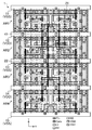
- FIG. 2 is a plan view showing a layout configuration example of a standard cell included in the semiconductor integrated circuit device according to the first embodiment.
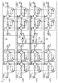
- Circuit diagram of the standard cell in FIG. 1 is a transistor level circuit diagram of a partial circuit included in the standard cell of FIG.
- the top view which shows the layout structure of the partial circuit of FIG. FIG. 1 is a diagram in which a common signal supply path is highlighted in the layout of FIG.
- FIG. 1 is a diagram in which a common signal supply path is highlighted in the layout of FIG. Circuit diagram of standard cell provided in semiconductor integrated circuit device according to second embodiment.
- the semiconductor integrated circuit device includes a plurality of standard cells, and at least some of the plurality of standard cells are multi-height cells.
- a region sandwiched between a power supply wiring that supplies VDD and a power supply wiring that supplies VSS is referred to as a height region.
- a double height cell has two height regions sandwiched between three power supply lines.
- FIG. 1 is a plan view showing a layout configuration example of a standard cell 1 provided in the semiconductor integrated circuit device according to the first embodiment.
- the horizontal direction of the drawing is the X direction (corresponding to the first direction)
- the vertical direction of the drawing is the Y direction (corresponding to the second direction).
- FIG. 2 is a circuit diagram of the standard cell 1 of FIG.
- the standard cell 1 includes five power supply lines 11 to 15 extending in the X direction.
- the first power supply wirings 12 and 14 that supply VDD (first power supply potential) and the second power supply wirings 11, 13, and 15 that supply VSS (second power supply potential) are alternately arranged in the Y direction.
- Four height regions AR1 to AR4 are formed between the power supply wirings 11 to 15. That is, the standard cell 1 is a so-called quad height cell having a cell height four times that of a single height cell.
- Each of the height regions AR1 to AR4 is formed with a fin FET (Field Effect Transistor), and a predetermined circuit function is realized by these finFETs.
- a fin FET Field Effect Transistor
- the fin FET is configured by a gate wiring (Gate) 2 and a fin (Fin) 3.
- LI is a local wiring directly connected to the gate wiring 2 and the fin 3
- M1 is a metal wiring layer above the local wiring
- M2 is an upper metal wiring layer of M1
- VIA0 connects the local wiring and the M1 wiring.
- a via, VIA1 is a via that connects the M1 wiring and the M2 wiring.
- the power supply wires 11 to 15 are formed in the metal wiring layer M1. Note that the resistance value of the gate wiring and the local wiring is larger than the resistance value of the metal wiring such as the M1 wiring and the M2 wiring.
- the standard cell 1 is an 8-bit selector, and includes eight selectors SL0 to SL7 as partial circuits.
- Each selector SL * (* is an integer from 0 to 7) has two inputs D * 0 and D * 1 and one output X *, and is complementary to the select signal S and the select signal S.
- the inversion select signal NS is received as a common signal.
- Each selector SL * outputs the input D * 1 as the output X * when the select signal S is high (inverted select signal NS is low), and when the select signal S is low (inverted select signal NS is high).
- Input D * 0 is output as output X *.
- the select signal S is supplied from the outside of the standard cell 1.
- the inverted select signal NS is generated based on the select signal S by the common signal generating circuit 51 including the inverter 51a.
- the select signal S and the inverted select signal NS are supplied to the selectors SL0 to SL7 through the respective supply paths.
- the eight selectors SL0 to SL7 are arranged in each of the height areas AR1 to AR4. That is, selectors SL0 and SL1 are arranged in the height area AR1, selectors SL2 and SL3 are arranged in the height area AR2, selectors SL4 and SL5 are arranged in the height area AR3, and selectors SL6 and SL7 are arranged in the height area AR4. Yes.
- the select signal S is supplied to the height area AR2, and the common signal generation circuit 51 is disposed in the height area AR2.
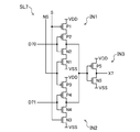
- FIG. 3 is a transistor level circuit diagram of a selector which is a partial circuit.
- FIG. 3 shows the selector SL7 as an example, but the configurations of the other selectors SL0 to SL6 are the same.
- Selector SL7 includes a tristate inverter IN1 that receives input D70, a tristate inverter IN2 that receives input D71, and an inverter IN3 that receives the outputs of tristate inverters IN1 and IN2.
- the tri-state inverter IN1 includes P-type transistors P1 and P2 and N-type transistors N1 and N2, and is connected in series in the order of P1, P2, N2, and N1 between VDD and VSS.
- the gate of the transistors P2 and N2 receives the input D70, and the connection end between the drains of the transistors P2 and N2 becomes the output of the tristate inverter IN1.
- the select signal S is applied to the gate of the transistor P1
- the inverted select signal NS is applied to the gate of the transistor N1.
- the tri-state inverter IN2 includes P-type transistors P3 and P4 and N-type transistors N3 and N4, and is connected in series in the order of P3, P4, N4, and N3 between VDD and VSS.
- the gates of the transistors P4 and N4 receive the input D71, and the connection ends of the drains of the transistors P4 and N4 become the output of the tristate inverter IN2.
- the select signal S is applied to the gate of the transistor N3, and the inverted select signal NS is applied to the gate of the transistor P3.
- the inverter IN3 includes a P-type transistor P5 and an N-type transistor N5 connected in series between VDD and VSS.
- the outputs of the tristate inverters IN1 and IN2 are received at the gates of the transistors P5 and N5, and the connection end between the drains of the transistors P5 and N5 becomes the output of the inverter IN3, that is, the output X7 of the selector SL7.
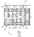
- FIG. 4 is a plan view showing a layout configuration of the selector SL7 of FIG. However, in FIG. 4, illustration of the M2 wiring and the via VIA1 is omitted.
- transistors P1, P2, P4, P3, and P5 are formed in order from the left.
- transistors N1, N2, N4, N3, and N5 are formed in order from the left.
- the layout of the selector SL6 arranged on the left side of the height area AR4 is a horizontally inverted version of the layout of FIG.
- the layout of the selectors SL2 and SL3 arranged in the height area AR2 is substantially the same as the layout of the selectors SL6 and SL7 arranged in the height area AR4.
- the layout of the selectors SL0 and SL1 arranged in the height area AR1 and the layout of the selectors SL4 and SL5 arranged in the height area AR3 are vertically inverted from the layout of the selectors SL6 and SL7 arranged in the height area AR4. It is almost the same.
- FIG. 5 is a diagram in which the supply path of the select signal S, which is a common signal, is highlighted in the layout of FIG.
- the supply path of the select signal S includes a metal wiring 21 disposed in the height area AR1 and a metal wiring 22 disposed in the height area AR3.
- the metal wiring 21 extends in the X direction in the height region AR1, and is connected to selectors SL0 and SL1 provided in the height region AR1.
- the metal wiring 22 extends in the X direction in the height region AR3 and is connected to selectors SL4 and SL5 provided in the height region AR3.
- the metal wirings 21 and 22 are formed in the same wiring layer M1 as the power supply wirings 11 to 15.
- the selection signal S supply path includes a gate wiring extending in the Y direction over a plurality of height regions, for example, a gate wiring 41 extending in the Y direction over the height regions AR1, AR2, AR3.
- FIG. 6 is a diagram in which the supply path of the inverted select signal NS that is a common signal is highlighted in the layout of FIG.
- the supply path of the inverted select signal NS includes a metal wiring 31 arranged in the height area AR2 and a metal wiring 32 arranged in the height area AR4.
- the metal wiring 31 extends in the X direction in the height region AR2, and is connected to selectors SL2 and SL3 provided in the height region AR2.
- the metal wiring 32 extends in the X direction in the height region AR4 and is connected to selectors SL6 and SL7 provided in the height region AR4.
- the metal wiring 31 is formed in the wiring layer M2 above the power supply wirings 11 to 15, and the metal wiring 32 is formed in the same wiring layer M1 as the power supply wirings 11 to 15.
- the standard cell 1 that is a multi-height cell
- two selectors SL0 to SL7 are arranged in the height regions AR1 to AR4.
- the metal wiring 21 constituting the supply path of the select signal S is arranged to connect the selectors SL0 and SL1 to the height area AR1, and the metal wiring 22 constituting the supply path of the select signal S is connected to the height area AR1.
- positions so that selector SL4, SL5 may be connected to area
- the resistance value in the supply path of the select signal S can be lowered, so that signal delay of the select signal S and voltage drop in the signal line can be suppressed. Accordingly, it is possible to realize speeding up and stabilization of the circuit operation of the standard cell 1.
- the metal wiring 31 constituting the supply path of the inverted select signal NS is arranged to connect the selectors SL2 and SL3 to the height region AR2, and the metal wiring 32 constituting the supply path of the inverted select signal NS is provided.
- the selectors SL6 and SL7 are connected to the height region AR4.
- the multi-height cell having four height regions AR1 to AR4 two eight selectors SL0 to SL7 are arranged in each height region AR1 to AR4.
- the disclosure is not limited to this.
- the number of height regions may be other than 4, and the number of selectors may be other than 8. Further, it is not necessary to arrange the same number of selectors in each height region.
- the metal wirings 21 and 22 are arranged in the height areas AR1 and AR3 for the supply path of the select signal S, and the metal wirings 31 and 32 are provided in the height areas AR2 and AR4 for the supply path of the inverted select signal NS.
- the present disclosure is not limited to this.
- the metal wiring constituting the supply path is arranged in two or more height regions, and the metal wiring is not arranged in the supply path for the other. May be.
- the metal wiring constituting the supply path is arranged in two or more height regions, and for the other one metal wiring constituting the supply path is provided. Alternatively, it may be arranged in two or more height regions.
- the height areas AR1 and AR3 in which the metal wirings 21 and 22 constituting the supply path of the select signal S are arranged, and the height areas AR2 and AR4 constituting the supply path of the inverted select signal NS are: It was assumed that they were alternately arranged in the Y direction. As a result, the resistance values of the supply paths can be adjusted to be approximately equal for the select signal S and the inverted select signal NS, so that signal delay and signal level can be balanced.
- the present disclosure is not limited to this.
- the metal wiring that constitutes the supply path of the select signal S may be arranged in a height region that is continuous in the Y direction, or inversion with the metal wiring that constitutes the supply path of the select signal S in the same height region.
- Metal wiring that constitutes the supply path of the select signal NS may be arranged.
- the metal wirings 21 and 22 constituting the supply path of the select signal S and the metal wirings 31 and 32 constituting the supply path of the inverted select signal NS are formed so as to extend in the X direction.
- the present disclosure is not limited to this.
- the metal wirings 21 and 22 constituting the supply path of the select signal S and the metal wirings 31 and 32 constituting the supply path of the inverted select signal NS are arranged so as to connect two selectors. However, it may be arranged to connect three or more selectors.
- FIG. 7 is a circuit diagram of the standard cell 2 provided in the semiconductor integrated circuit device according to the second embodiment.
- the standard cell 2 is an 8-bit FF (flip-flop), and includes eight flip-flops FF0 to FF7 as partial circuits.
- Each flip-flop FF * (* is an integer from 0 to 7) has an input D * and an output Q *, and operates by receiving the clock signal CK and the inverted clock signal NCK as a common signal.
- the clock signal CK and the inverted clock signal NCK complementary to the clock signal CK are based on the original clock signal CLK supplied from the outside of the standard cell 2 by the common signal generation circuit 52 including the inverters 52a and 52b. Generated.
- the clock signal CK and the inverted clock signal NCK are supplied to the flip-flops FF0 to FF7 through respective supply paths.
- the layout of the standard cell 2 is omitted here, but can be configured in the same manner as the standard cell 1 of the first embodiment. That is, the standard cell 2 includes five power supply wirings extending in the X direction. The first power supply wiring for supplying VDD and the second power supply wiring for supplying VSS are alternately arranged in the Y direction. Four height regions AR1 to AR4 are formed between the five power supply lines. That is, the standard cell 2 is a so-called quad height cell having a cell height four times that of a single height cell. Fin FETs are formed in the height regions AR1 to AR4, respectively, and a predetermined circuit function is realized by these fin FETs.
- the two eight flip-flops FF0 to FF7 are arranged in each of the height areas AR1 to AR4. That is, flip-flops FF0 and FF7 are arranged in the height area AR1, flip-flops FF1 and FF6 are arranged in the height area AR2, flip-flops FF2 and FF5 are arranged in the height area AR3, and flip-flops FF3 and FF4 are arranged in the height area AR4. Is arranged.
- the original clock signal CLK is supplied to the height region AR2, and the common signal generation circuit 52 is disposed in the height regions AR2 and AR3.
- the supply path of the clock signal CK includes a metal wiring 61 arranged in the height area AR1 and a metal wiring 62 arranged in the height area AR3.
- the metal wiring 61 extends in the X direction in the height region AR1, and is connected to flip-flops FF0 and FF7 provided in the height region AR1.
- the metal wiring 62 extends in the X direction in the height region AR3 and is connected to flip-flops FF2 and FF5 provided in the height region AR3.
- the supply path of the inverted clock signal NCK includes a metal wiring 71 disposed in the height region AR2 and a metal wiring 72 disposed in the height region AR4.
- the metal wiring 71 extends in the X direction in the height region AR2, and is connected to flip-flops FF1 and FF6 provided in the height region AR2.
- the metal wiring 72 extends in the X direction in the height region AR4 and is connected to flip-flops FF3 and FF4 provided in the height region AR4. Note that the metal wirings 61, 62, 71, 72 may be formed in the same wiring layer as the power supply wiring, or may be formed in a wiring layer above the power supply wiring.
- the standard cell 2 which is a multi-height cell
- two eight flip-flops FF0 to FF7 are arranged in the height regions AR1 to AR4.
- the metal wiring 61 constituting the clock signal CK supply path is arranged to connect the flip-flops FF0 and FF7 to the height region AR1, and the metal wiring 62 constituting the clock signal CK supply path is
- the flip-flops FF2 and FF5 are arranged to be connected to the height area AR3.
- the resistance value in the supply path of the clock signal CK can be lowered, so that signal delay of the clock signal CK and voltage drop in the signal line can be suppressed. Accordingly, it is possible to realize speeding up and stabilization of the circuit operation of the standard cell 2.
- a metal wiring 71 that constitutes a supply path of the inverted clock signal NCK is disposed so as to connect the flip-flops FF1 and FF6 to the height region AR2, and a metal wiring 72 that constitutes a supply path of the inverted clock signal NCK.
- the flip-flops FF3 and FF4 are connected to the height area AR4.
- the resistance value in the supply path of the inverted clock signal NCK can be lowered, so that signal delay of the inverted clock signal NCK and voltage drop in the signal line can be suppressed. Accordingly, it is possible to realize speeding up and stabilization of the circuit operation of the standard cell 2.
- the multi-height cell having four height regions AR1 to AR4 two eight flip-flops FF0 to FF7 are arranged in each height region AR1 to AR4.
- the present disclosure is not limited to this.
- the number of height regions may be other than 4, and the number of flip-flops may be other than 8. Further, it is not necessary to arrange the same number of flip-flops in each height region.
- the metal wirings 61 and 62 are disposed in the height regions AR1 and AR3 with respect to the supply path of the clock signal CK, and the metal wirings 71 and 72 are provided in the height regions AR2 and AR4 with respect to the supply path of the inverted clock signal NCK.
- the present disclosure is not limited to this.
- the metal wiring constituting the supply path is arranged in two or more height regions, and the metal wiring is not arranged in the supply path for the other. May be.
- the metal wiring constituting the supply path is arranged in two or more height regions, and for the other, one metal wiring constituting the supply path is provided. Alternatively, it may be arranged in two or more height regions.
- the height regions AR1 and AR3 in which the metal wirings 61 and 62 that constitute the supply path of the clock signal CK are arranged and the height regions AR2 and AR4 that constitute the supply path of the inverted clock signal NCK are: It was assumed that they were alternately arranged in the Y direction. As a result, the resistance values of the supply paths can be adjusted to be approximately equal for the clock signal CK and the inverted clock signal NCK, so that signal delay and signal level can be balanced.
- the present disclosure is not limited to this.
- the metal wiring that configures the supply path of the clock signal CK may be arranged in a height region that is continuous in the Y direction, or is inverted to the metal wiring that configures the supply path of the clock signal CK in the same height region.
- Metal wiring that constitutes a supply path of the clock signal NCK may be disposed.
- the metal wirings 61 and 62 constituting the supply path of the clock signal CK and the metal wirings 71 and 72 constituting the supply path of the inverted clock signal NCK are formed so as to extend in the X direction.
- the present disclosure is not limited to this.
- the metal wirings 61 and 62 constituting the supply path of the clock signal CK and the metal wirings 71 and 72 constituting the supply path of the inverted clock signal NCK are provided so as to connect two flip-flops. However, it may be arranged so that three or more flip-flops are connected.
- the selector and the flip-flop have been described as examples of the partial circuit constituting the standard cell.
- the partial circuit constituting the standard cell is not limited to these.
- a latch may be used.
- the common signals to be given to the plurality of partial circuits are limited to these. is not.
- the configuration of the present disclosure may be applied to a reset signal, a set signal, a scan mode signal, and the like.
- the standard cell having a plurality of partial circuits is configured using the fin FET.
- the transistor configuring the standard cell is not limited to the fin FET.
- This disclosure is useful for improving the performance of a semiconductor integrated circuit device because a multi-height cell having a plurality of partial circuits can realize high-speed and stable circuit operation.
Landscapes
- Design And Manufacture Of Integrated Circuits (AREA)
- Engineering & Computer Science (AREA)
- General Engineering & Computer Science (AREA)
- Semiconductor Integrated Circuits (AREA)
Abstract
半導体集積回路装置における、複数のハイト領域(AR1~AR4)を有するスタンダードセル(1)において、互いに同一の機能を持ち、共通信号S,NSを受けてそれぞれ動作する複数の部分回路(SL0~SL7)が、それぞれ、ハイト領域(AR1~AR4)のいずれかに配置されている。ハイト領域(AR1)には、共通信号Sの供給経路を構成するメタル配線(21)が部分回路(SL0,SL1)に接続されるように配置され、ハイト領域(AR3)には、共通信号Sの供給経路を構成するメタル配線(22)が部分回路(SL4,SL5)に接続されるように配置されている。
Description
本開示は、マルチハイトセルを備えた半導体集積回路装置に関する。
半導体基板上に半導体集積回路を形成する方法として、スタンダードセル方式が知られている。スタンダードセル方式とは、特定の論理機能を有する基本的単位(例えば、インバータ,ラッチ,フリップフロップ,全加算器など)をスタンダードセルとして予め用意しておき、半導体基板上に複数のスタンダードセルを配置して、それらのスタンダードセルを配線で接続することによって、LSIチップを設計する方式のことである。
また近年、半導体集積回路の高速化や小面積化のために、スタンダードセルにマルチハイト構造を適用することが行われている。マルチハイト構造が適用されたスタンダードセルすなわちマルチハイトセルは、シングルハイトセルをセル高さ方向に複数個連結させた構造をしており、そのセル高さはシングルハイトセルのセル高さのn倍(nは2以上の整数)である。
特許文献1では、マルチハイトセルの一例として、セル高さがシングルハイトセルのセル高さの2倍であるダブルハイトセルのレイアウト構成が示されている。
スタンダードセルの回路機能の1つとして、マルチビットセレクタのように、互いに同一の機能を持つ複数の部分回路(ここではセレクタ)を有するものがある。このような回路機能では、各部分回路はセレクト信号などの共通信号を受けてそれぞれ動作する。このようなスタンダードセルをマルチハイトセルで実現する場合には、各部分回路に与える共通信号の供給経路が長くなり、その抵抗値が高くなってしまう可能性がある。共通信号の供給経路の抵抗値が高いと、信号遅延が大きくなるため回路の高速動作が困難になるとともに、信号線における電圧降下が大きくなるため回路の動作が不安定になってしまう。
本開示は、半導体集積回路装置において、複数の部分回路を有するマルチハイトセルについて、回路動作の高速化および安定化を実現できる構成を提供する。
本開示の態様では、半導体集積回路装置は、所定の回路機能を実現するスタンダードセルを備え、前記スタンダードセルは、第1方向にそれぞれ延びており、前記第1方向と垂直をなす第2方向において、第1電源電位を供給する第1電源配線と第2電源電位を供給する第2電源配線とが交互に配置された、N(Nは3以上の整数)本の電源配線と、互いに同一の機能を持ち、かつ、1つまたは複数種類の共通信号を受けてそれぞれ動作する、複数の部分回路とを備え、前記複数の部分回路は、それぞれ、前記第1電源配線と前記第2電源配線とに挟まれた領域であるM(M=N-1)個のハイト領域のいずれかに、配置されており、前記M個のハイト領域のうち少なくとも2つである第1ハイト領域は、それぞれ、前記部分回路が複数個、配置されており、かつ、前記共通信号のうちの1つである第1共通信号の供給経路を構成するメタル配線が、少なくとも2個の前記部分回路に接続されるように配置されている。
この態様によると、所定の回路機能を実現するスタンダードセルは、第1電源電位を供給する第1電源配線と第2電源電位を供給する第2電源配線とに挟まれた領域であるハイト領域を、2個以上備えており、いわゆるマルチハイトセルである。このスタンダードセルにおいて、互いに同一の機能を持ち、かつ、1つまたは複数種類の共通信号を受けてそれぞれ動作する複数の部分回路は、それぞれ、ハイト領域のいずれかに配置されている。そして、部分回路が複数個配置された少なくとも2つの第1ハイト領域には、それぞれ、第1共通信号の供給経路を構成するメタル配線が、少なくとも2個の部分回路に接続されるように配置されている。これにより、第1共通信号の供給経路における抵抗値を下げることができるので、信号遅延の抑制による回路動作の高速化や、信号線における電圧降下の低減による回路動作の安定化を実現することができる。
本開示によると、複数の部分回路を有するマルチハイトセルにおいて、部分回路に与える共通信号の供給経路における抵抗値を下げることができるので、回路動作の高速化や安定化を実現することができる。
以下、実施の形態について、図面を参照して説明する。以下の実施の形態では、半導体集積回路装置は複数のスタンダードセルを備えており、この複数のスタンダードセルのうち少なくとも一部は、マルチハイトセルであるものとする。また、本開示では、マルチハイトセルにおいて、VDDを供給する電源配線とVSSを供給する電源配線とに挟まれた領域のことを、ハイト領域という。例えば、ダブルハイトセルは、3本の電源配線同士の間に挟まれた、2個のハイト領域を有している。
(第1実施形態)
図1は第1実施形態に係る半導体集積回路装置が備えたスタンダードセル1のレイアウト構成例を示す平面図である。図1では、図面横方向をX方向(第1方向に相当)とし、図面縦方向をY方向(第2方向に相当)としている。以降のレイアウト平面図についても同様である。また、図2は図1のスタンダードセル1の回路図である。
図1は第1実施形態に係る半導体集積回路装置が備えたスタンダードセル1のレイアウト構成例を示す平面図である。図1では、図面横方向をX方向(第1方向に相当)とし、図面縦方向をY方向(第2方向に相当)としている。以降のレイアウト平面図についても同様である。また、図2は図1のスタンダードセル1の回路図である。
図1に示すように、スタンダードセル1は、X方向にそれぞれ延びる5本の電源配線11~15を備えている。VDD(第1電源電位)を供給する第1電源配線12,14とVSS(第2電源電位)を供給する第2電源配線11,13,15とは、Y方向において交互に配置されている。電源配線11~15同士の間に4個のハイト領域AR1~AR4が形成されている。すなわち、スタンダードセル1は、シングルハイトセルの4倍のセル高さを有する、いわゆるクワッドハイト(quad height)セルである。ハイト領域AR1~AR4にはそれぞれ、フィンFET(Field Effect Transistor)が形成されており、これらのフィンFETによって所定の回路機能が実現されている。フィンFETは、ゲート配線(Gate)2とフィン(Fin)3とによって構成される。また、LIはゲート配線2およびフィン3と直接接続されるローカル配線、M1はローカル配線の上層のメタル配線層、M2はM1の上層のメタル配線層、VIA0はローカル配線とM1配線とを接続するビア、VIA1はM1配線とM2配線とを接続するビアである。電源配線11~15はメタル配線層M1に形成されている。なお、ゲート配線およびローカル配線の抵抗値は、M1配線、M2配線等のメタル配線の抵抗値よりも大きい。
図2に示すように、スタンダードセル1は8ビットセレクタであり、8個のセレクタSL0~SL7を部分回路として備えている。各セレクタSL*(*は0~7の整数)は、2個の入力D*0,D*1と1個の出力X*とを備えており、セレクト信号Sおよび、セレクト信号Sと相補関係にある反転セレクト信号NSを共通信号として受けて動作する。各セレクタSL*は、セレクト信号Sがハイ(反転セレクト信号NSがロー)のときは入力D*1を出力X*として出力し、セレクト信号Sがロー(反転セレクト信号NSがハイ)のときは入力D*0を出力X*として出力する。セレクト信号Sは、スタンダードセル1の外部から供給される。反転セレクト信号NSは、インバータ51aを備えた共通信号生成回路51によって、セレクト信号Sを基にして生成される。セレクト信号Sおよび反転セレクト信号NSは、それぞれの供給経路を経て、各セレクタSL0~SL7に供給される。
8個のセレクタSL0~SL7は、ハイト領域AR1~AR4にそれぞれ2個ずつ、配置されている。すなわち、ハイト領域AR1にセレクタSL0,SL1が配置され、ハイト領域AR2にセレクタSL2,SL3が配置され、ハイト領域AR3にセレクタSL4,SL5が配置され、ハイト領域AR4にセレクタSL6,SL7が配置されている。セレクト信号Sはハイト領域AR2に供給され、また、共通信号生成回路51はハイト領域AR2に配置されている。
図3は部分回路であるセレクタのトランジスタレベルの回路図である。図3では、セレクタSL7を例にとって示しているが、他のセレクタSL0~SL6の構成も同様である。セレクタSL7は、入力D70を受けるトライステートインバータIN1と、入力D71を受けるトライステートインバータIN2と、トライステートインバータIN1,IN2の出力を受けるインバータIN3とを備える。トライステートインバータIN1は、P型トランジスタP1,P2およびN型トランジスタN1,N2を備え、VDDとVSSとの間にP1,P2,N2,N1の順に直列接続されている。トランジスタP2,N2のゲートに入力D70を受け、トランジスタP2,N2のドレイン同士の接続端がトライステートインバータIN1の出力となる。また、セレクト信号SはトランジスタP1のゲートに与えられ、反転セレクト信号NSはトランジスタN1のゲートに与えられる。トライステートインバータIN2は、P型トランジスタP3,P4およびN型トランジスタN3,N4を備え、VDDとVSSとの間にP3,P4,N4,N3の順に直列接続されている。トランジスタP4,N4のゲートに入力D71を受け、トランジスタP4,N4のドレイン同士の接続端がトライステートインバータIN2の出力となる。また、セレクト信号SはトランジスタN3のゲートに与えられ、反転セレクト信号NSはトランジスタP3のゲートに与えられる。インバータIN3はVDDとVSSとの間に直列接続されたP型トランジスタP5およびN型トランジスタN5を備える。トランジスタP5,N5のゲートにトライステートインバータIN1,IN2の出力を受け、トランジスタP5,N5のドレイン同士の接続端がインバータIN3の出力、すなわち、セレクタSL7の出力X7となる。
図4は図3のセレクタSL7のレイアウト構成を示す平面図である。ただし、図4において、M2配線とビアVIA1については、図示を省略している。第1電源配線14側のP型トランジスタ領域において、左から順にトランジスタP1,P2,P4,P3,P5が形成されている。第2電源配線15側のN型トランジスタ領域において、左から順にトランジスタN1,N2,N4,N3,N5が形成されている。
図4のレイアウトは、図1のレイアウトにおけるハイト領域AR4の右側部分に相当する。ハイト領域AR4の左側に配置されるセレクタSL6のレイアウトは、図4のレイアウトを左右反転させたものになる。ハイト領域AR2に配置されるセレクタSL2,SL3のレイアウトは、ハイト領域AR4に配置されるセレクタSL6,SL7のレイアウトとほぼ同様である。また、ハイト領域AR1に配置されるセレクタSL0,SL1のレイアウト、および、ハイト領域AR3に配置されるセレクタSL4,SL5のレイアウトは、ハイト領域AR4に配置されるセレクタSL6,SL7のレイアウトを上下反転させたものとほぼ同様である。
図5は図1のレイアウトにおいて、共通信号であるセレクト信号Sの供給経路を強調表示した図である。図5では、セレクト信号Sの供給経路について、メタル配線、ローカル配線およびゲート配線の輪郭を太く示し、また、ゲート配線のハッチを黒塗りに替えている。図5に示すように、セレクト信号Sの供給経路は、ハイト領域AR1に配置されたメタル配線21と、ハイト領域AR3に配置されたメタル配線22とを含む。メタル配線21は、ハイト領域AR1においてX方向に延びており、ハイト領域AR1に設けられたセレクタSL0,SL1に接続されている。メタル配線22は、ハイト領域AR3においてX方向に延びており、ハイト領域AR3に設けられたセレクタSL4,SL5に接続されている。ここでは、メタル配線21,22は、電源配線11~15と同一の配線層M1に形成されている。また、セレクト信号Sの供給経路は、複数のハイト領域にわたってY方向に延びるゲート配線、例えばハイト領域AR1,AR2,AR3にわたってY方向に延びるゲート配線41を含む。
図6は図1のレイアウトにおいて、共通信号である反転セレクト信号NSの供給経路を強調表示した図である。図6では、反転セレクト信号Sの供給経路について、メタル配線、ローカル配線およびゲート配線の輪郭を太く示し、また、ゲート配線のハッチを黒塗りに替えている。図6に示すように、反転セレクト信号NSの供給経路は、ハイト領域AR2に配置されたメタル配線31と、ハイト領域AR4に配置されたメタル配線32とを含む。メタル配線31は、ハイト領域AR2においてX方向に延びており、ハイト領域AR2に設けられたセレクタSL2,SL3に接続されている。メタル配線32は、ハイト領域AR4においてX方向に延びており、ハイト領域AR4に設けられたセレクタSL6,SL7に接続されている。ここでは、メタル配線31は、電源配線11~15より上層の配線層M2に形成されており、メタル配線32は、電源配線11~15と同一の配線層M1に形成されている。
以上のように本実施形態によると、マルチハイトセルであるスタンダードセル1において、8個のセレクタSL0~SL7は、ハイト領域AR1~AR4に2個ずつ、配置されている。そして、セレクト信号Sの供給経路を構成するメタル配線21が、ハイト領域AR1に、セレクタSL0,SL1を接続するように配置されており、セレクト信号Sの供給経路を構成するメタル配線22が、ハイト領域AR3に、セレクタSL4,SL5を接続するように配置されている。これにより、セレクト信号Sの供給経路における抵抗値を下げることができるので、セレクト信号Sの信号遅延や信号線における電圧降下を抑制することができる。したがって、スタンダードセル1の回路動作の高速化や安定化を実現することができる。
また、反転セレクト信号NSの供給経路を構成するメタル配線31が、ハイト領域AR2に、セレクタSL2,SL3を接続するように配置されており、反転セレクト信号NSの供給経路を構成するメタル配線32が、ハイト領域AR4に、セレクタSL6,SL7を接続するように配置されている。これにより、反転セレクト信号NSの供給経路における抵抗値を下げることができるので、反転セレクト信号NSの信号遅延や信号線における電圧降下を抑制することができる。したがって、スタンダードセル1の回路動作の高速化や安定化を実現することができる。
なお、本実施形態では、4個のハイト領域AR1~AR4を備えたマルチハイトセルにおいて、8個のセレクタSL0~SL7を、各ハイト領域AR1~AR4に2個ずつ配置するものとしたが、本開示はこれに限られるものではない。例えば、ハイト領域の個数は4個以外であってもよいし、セレクタの個数は8個以外であってもよい。また、各ハイト領域に同一個数のセレクタを配置しなくてもよい。
また、本実施形態では、セレクト信号Sの供給経路について、ハイト領域AR1,AR3にメタル配線21,22を配置し、反転セレクト信号NSの供給経路について、ハイト領域AR2,AR4にメタル配線31,32を配置するものとしたが、本開示はこれに限られるものではない。例えば、セレクト信号Sと反転セレクト信号NSのうちいずれか一方について、その供給経路を構成するメタル配線を2個以上のハイト領域に配置し、他方について、その供給経路にメタル配線を配置しないようにしてもよい。あるいは、セレクト信号Sと反転セレクト信号NSのうちいずれか一方について、その供給経路を構成するメタル配線を2個以上のハイト領域に配置し、他方について、その供給経路を構成するメタル配線を1つまたは2個以上のハイト領域に配置してもよい。
また、本実施形態では、セレクト信号Sの供給経路を構成するメタル配線21,22が配置されるハイト領域AR1,AR3と、反転セレクト信号NSの供給経路を構成するハイト領域AR2,AR4とは、Y方向において交互に配置されているものとした。これにより、セレクト信号Sと反転セレクト信号NSとについて、供給経路の抵抗値をほぼ同等に合わせることができるので、信号遅延や信号レベルのバランスをとることができる。ただし、本開示はこれに限られるものではない。例えば、セレクト信号Sの供給経路を構成するメタル配線が、Y方向において連続するハイト領域に配置されていてもよいし、同じハイト領域に、セレクト信号Sの供給経路を構成するメタル配線と、反転セレクト信号NSの供給経路を構成するメタル配線とが配置されていてもよい。
また、本実施形態では、セレクト信号Sの供給経路を構成するメタル配線21,22、および、反転セレクト信号NSの供給経路を構成するメタル配線31,32は、X方向に延びるように形成されているものとしたが、本開示はこれに限られるものではない。また、セレクト信号Sの供給経路を構成するメタル配線21,22、および、反転セレクト信号NSの供給経路を構成するメタル配線31,32は、2個のセレクタを接続するように配置されているものとしたが、3個以上のセレクタを接続するように配置してもよい。
(第2実施形態)
図7は第2実施形態に係る半導体集積回路装置が備えたスタンダードセル2の回路図である。図7に示すように、スタンダードセル2は8ビットFF(フリップフロップ)であり、8個のフリップフロップFF0~FF7を部分回路として備えている。各フリップフロップFF*(*は0~7の整数)は、入力D*と出力Q*とを備えており、クロック信号CKおよび反転クロック信号NCKを共通信号として受けて動作する。クロック信号CKおよび、クロック信号CKと相補関係にある反転クロック信号NCKは、インバータ52a,52bを備えた共通信号生成回路52によって、スタンダードセル2の外部から供給される原クロック信号CLKを基にして生成される。クロック信号CKおよび反転クロック信号NCKは、それぞれの供給経路を経て、各フリップフロップFF0~FF7に供給される。
図7は第2実施形態に係る半導体集積回路装置が備えたスタンダードセル2の回路図である。図7に示すように、スタンダードセル2は8ビットFF(フリップフロップ)であり、8個のフリップフロップFF0~FF7を部分回路として備えている。各フリップフロップFF*(*は0~7の整数)は、入力D*と出力Q*とを備えており、クロック信号CKおよび反転クロック信号NCKを共通信号として受けて動作する。クロック信号CKおよび、クロック信号CKと相補関係にある反転クロック信号NCKは、インバータ52a,52bを備えた共通信号生成回路52によって、スタンダードセル2の外部から供給される原クロック信号CLKを基にして生成される。クロック信号CKおよび反転クロック信号NCKは、それぞれの供給経路を経て、各フリップフロップFF0~FF7に供給される。
スタンダードセル2のレイアウトについては、ここでは図示を省略するが、第1実施形態のスタンダードセル1と同様に構成することができる。すなわち、スタンダードセル2は、X方向にそれぞれ延びる5本の電源配線を備えている。VDDを供給する第1電源配線とVSSを供給する第2電源配線とは、Y方向において交互に配置されている。5本の電源配線同士の間に4個のハイト領域AR1~AR4が形成されている。すなわち、スタンダードセル2は、シングルハイトセルの4倍のセル高さを有する、いわゆるクワッドハイト(quad height)セルである。ハイト領域AR1~AR4にはそれぞれ、フィンFETが形成されており、これらのフィンFETによって所定の回路機能が実現されている。
8個のフリップフロップFF0~FF7は、ハイト領域AR1~AR4にそれぞれ2個ずつ、配置されている。すなわち、ハイト領域AR1にフリップフロップFF0,FF7が配置され、ハイト領域AR2にフリップフロップFF1,FF6が配置され、ハイト領域AR3にフリップフロップFF2,FF5が配置され、ハイト領域AR4にフリップフロップFF3,FF4が配置されている。原クロック信号CLKはハイト領域AR2に供給され、また、共通信号生成回路52はハイト領域AR2,AR3に配置されている。
そして、クロック信号CKの供給経路は、ハイト領域AR1に配置されたメタル配線61と、ハイト領域AR3に配置されたメタル配線62とを含む。メタル配線61は、ハイト領域AR1においてX方向に延びており、ハイト領域AR1に設けられたフリップフロップFF0,FF7に接続されている。メタル配線62は、ハイト領域AR3においてX方向に延びており、ハイト領域AR3に設けられたフリップフロップFF2,FF5に接続されている。また、反転クロック信号NCKの供給経路は、ハイト領域AR2に配置されたメタル配線71と、ハイト領域AR4に配置されたメタル配線72とを含む。メタル配線71は、ハイト領域AR2においてX方向に延びており、ハイト領域AR2に設けられたフリップフロップFF1,FF6に接続されている。メタル配線72は、ハイト領域AR4においてX方向に延びており、ハイト領域AR4に設けられたフリップフロップFF3,FF4に接続されている。なお、メタル配線61,62,71,72は例えば、電源配線と同一の配線層に形成されていてもよいし、電源配線よりも上層の配線層に形成されていてもよい。
以上のように本実施形態によると、マルチハイトセルであるスタンダードセル2において、8個のフリップフロップFF0~FF7は、ハイト領域AR1~AR4に2個ずつ、配置されている。そして、クロック信号CKの供給経路を構成するメタル配線61が、ハイト領域AR1に、フリップフロップFF0,FF7を接続するように配置されており、クロック信号CKの供給経路を構成するメタル配線62が、ハイト領域AR3に、フリップフロップFF2,FF5を接続するように配置されている。これにより、クロック信号CKの供給経路における抵抗値を下げることができるので、クロック信号CKの信号遅延や信号線における電圧降下を抑制することができる。したがって、スタンダードセル2の回路動作の高速化や安定化を実現することができる。
また、反転クロック信号NCKの供給経路を構成するメタル配線71が、ハイト領域AR2に、フリップフロップFF1,FF6を接続するように配置されており、反転クロック信号NCKの供給経路を構成するメタル配線72が、ハイト領域AR4に、フリップフロップFF3,FF4を接続するように配置されている。これにより、反転クロック信号NCKの供給経路における抵抗値を下げることができるので、反転クロック信号NCKの信号遅延や信号線における電圧降下を抑制することができる。したがって、スタンダードセル2の回路動作の高速化や安定化を実現することができる。
なお、本実施形態では、4個のハイト領域AR1~AR4を備えたマルチハイトセルにおいて、8個のフリップフロップFF0~FF7を、各ハイト領域AR1~AR4に2個ずつ配置するものとしたが、本開示はこれに限られるものではない。例えば、ハイト領域の個数は4個以外であってもよいし、フリップフロップの個数は8個以外であってもよい。また、各ハイト領域に同一個数のフリップフロップを配置しなくてもよい。
また、本実施形態では、クロック信号CKの供給経路について、ハイト領域AR1,AR3にメタル配線61,62を配置し、反転クロック信号NCKの供給経路について、ハイト領域AR2,AR4にメタル配線71,72を配置するものとしたが、本開示はこれに限られるものではない。例えば、クロック信号CKと反転クロック信号NCKのうちいずれか一方について、その供給経路を構成するメタル配線を2個以上のハイト領域に配置し、他方について、その供給経路にメタル配線を配置しないようにしてもよい。あるいは、クロック信号CKと反転クロック信号NCKのうちいずれか一方について、その供給経路を構成するメタル配線を2個以上のハイト領域に配置し、他方について、その供給経路を構成するメタル配線を1つまたは2個以上のハイト領域に配置してもよい。
また、本実施形態では、クロック信号CKの供給経路を構成するメタル配線61,62が配置されるハイト領域AR1,AR3と、反転クロック信号NCKの供給経路を構成するハイト領域AR2,AR4とは、Y方向において交互に配置されているものとした。これにより、クロック信号CKと反転クロック信号NCKとについて、供給経路の抵抗値をほぼ同等に合わせることができるので、信号遅延や信号レベルのバランスをとることができる。ただし、本開示はこれに限られるものではない。例えば、クロック信号CKの供給経路を構成するメタル配線が、Y方向において連続するハイト領域に配置されていてもよいし、同じハイト領域に、クロック信号CKの供給経路を構成するメタル配線と、反転クロック信号NCKの供給経路を構成するメタル配線とが配置されていてもよい。
また、本実施形態では、クロック信号CKの供給経路を構成するメタル配線61,62、および、反転クロック信号NCKの供給経路を構成するメタル配線71,72は、X方向に延びるように形成されているものとしたが、本開示はこれに限られるものではない。また、クロック信号CKの供給経路を構成するメタル配線61,62、および、反転クロック信号NCKの供給経路を構成するメタル配線71,72は、2個のフリップフロップを接続するように設けられているものとしたが、3個以上のフリップフロップを接続するように配置してもよい。
(他の実施形態)
上述した実施形態では、スタンダードセルを構成する部分回路として、セレクタやフリップフロップを例にとって説明を行ったが、本開示において、スタンダードセルを構成する部分回路はこれらに限られるものではない。例えば、ラッチであってもよい。
上述した実施形態では、スタンダードセルを構成する部分回路として、セレクタやフリップフロップを例にとって説明を行ったが、本開示において、スタンダードセルを構成する部分回路はこれらに限られるものではない。例えば、ラッチであってもよい。
また、上述した実施形態では、複数の部分回路に与える共通信号として、セレクト信号やクロック信号を例にとって説明を行ったが、本開示において、複数の部分回路に与える共通信号はこれらに限られるものではない。例えば、リセット信号、セット信号、スキャンモード信号等について、本開示の構成を適用してもよい。
また、上述した実施形態では、複数の部分回路を有するスタンダードセルを、フィンFETを用いて構成するものとしたが、本開示において、スタンダードセルを構成するトランジスタはフィンFETに限られるものではない。
なお、発明の趣旨を逸脱しない範囲で、複数の実施形態における各構成要素を任意に組み合わせてもよい。
本開示では、複数の部分回路を有するマルチハイトセルにおいて、回路動作の高速化や安定化を実現できるので、半導体集積回路装置の性能向上に有用である。
1,2 スタンダードセル
11,13,15 第1電源配線
12,14 第2電源配線
21,22,31,32 メタル配線
41 ゲート配線
51,52 共通信号生成回路
61,62,71,72 メタル配線
AR1~AR4 ハイト領域
FF0~FF7 フリップフロップ(部分回路)
SL0~SL7 セレクタ(部分回路)
S セレクト信号(共通信号)
NS 反転セレクト信号(共通信号)
CK クロック信号(共通信号)
NCK 反転クロック信号(共通信号)
11,13,15 第1電源配線
12,14 第2電源配線
21,22,31,32 メタル配線
41 ゲート配線
51,52 共通信号生成回路
61,62,71,72 メタル配線
AR1~AR4 ハイト領域
FF0~FF7 フリップフロップ(部分回路)
SL0~SL7 セレクタ(部分回路)
S セレクト信号(共通信号)
NS 反転セレクト信号(共通信号)
CK クロック信号(共通信号)
NCK 反転クロック信号(共通信号)
Claims (19)
- 所定の回路機能を実現するスタンダードセルを備え、
前記スタンダードセルは、
第1方向にそれぞれ延びており、前記第1方向と垂直をなす第2方向において、第1電源電位を供給する第1電源配線と第2電源電位を供給する第2電源配線とが交互に配置された、N(Nは3以上の整数)本の電源配線と、
1つまたは複数種類の共通信号を受けてそれぞれ動作する、複数のフリップフロップ回路とを備え、
前記複数のフリップフロップ回路は、それぞれ、前記第1電源配線と前記第2電源配線とに挟まれた領域であるM(M=N-1)個のハイト領域のいずれかに、配置されており、
前記M個のハイト領域のうち少なくとも2つである第1ハイト領域は、それぞれ、前記フリップフロップ回路が複数個、配置されており、かつ、前記共通信号のうちの1つである第1共通信号の供給経路を構成するメタル配線が、少なくとも2個の前記フリップフロップ回路に接続されるように配置されている
ことを特徴とする半導体集積回路装置。 - 請求項1記載の半導体集積回路装置において、
前記スタンダードセルは、前記第1共通信号を生成する共通信号生成回路を備えている
ことを特徴とする半導体集積回路装置。 - 請求項1記載の半導体集積回路装置において、
前記第1共通信号の供給経路は、前記M個のハイト領域のうちの隣り合う2個以上のハイト領域にわたって、前記第2方向に延びるように形成されたゲート配線を含む
ことを特徴とする半導体集積回路装置。 - 請求項1記載の半導体集積回路装置において、
前記M個のハイト領域は、前記第1共通信号の供給経路を構成するメタル配線が設けられていないハイト領域を含む
ことを特徴とする半導体集積回路装置。 - 請求項1記載の半導体集積回路装置において、
前記第1ハイト領域に配置されており、前記第1共通信号の供給経路を構成するメタル配線は、前記第1方向に延びるように形成されている
ことを特徴とする半導体集積回路装置。 - 請求項1記載の半導体集積回路装置において、
前記第1共通信号は、クロック信号である
ことを特徴とする半導体集積回路装置。 - 請求項6記載の半導体集積回路装置において、
前記共通信号は、前記クロック信号の反転信号である反転クロック信号を含み、
前記M個のハイト領域のうち少なくとも1つである第2ハイト領域は、前記フリップフロップ回路が複数個、配置されており、かつ、前記反転クロック信号の供給経路を構成する第2メタル配線が、少なくとも2個の前記フリップフロップ回路に接続されるように配置されている
ことを特徴とする半導体集積回路装置。 - 請求項7記載の半導体集積回路装置において、
前記第2ハイト領域は、前記第1ハイト領域と異なるハイト領域である
ことを特徴とする半導体集積回路装置。 - 請求項8記載の半導体集積回路装置において、
前記M個のハイト領域は、前記第1ハイト領域と前記第2ハイト領域とが、前記第2方向において交互に配置されている
ことを特徴とする半導体集積回路装置。 - 所定の回路機能を実現するスタンダードセルを備え、
前記スタンダードセルは、
第1方向にそれぞれ延びており、前記第1方向と垂直をなす第2方向において、第1電源電位を供給する第1電源配線と第2電源電位を供給する第2電源配線とが交互に配置された、N(Nは3以上の整数)本の電源配線と、
互いに同一の機能を持ち、かつ、1つまたは複数種類の共通信号を受けてそれぞれ動作する、複数の部分回路とを備え、
前記複数の部分回路は、それぞれ、前記第1電源配線と前記第2電源配線とに挟まれた領域であるM(M=N-1)個のハイト領域のいずれかに、配置されており、
前記M個のハイト領域のうち少なくとも2つである第1ハイト領域は、それぞれ、前記部分回路が複数個、配置されており、かつ、前記共通信号のうちの1つである第1共通信号の供給経路を構成するメタル配線が、少なくとも2個の前記部分回路に接続されるように配置されている
ことを特徴とする半導体集積回路装置。 - 請求項10記載の半導体集積回路装置において、
前記スタンダードセルは、前記第1共通信号を生成する共通信号生成回路を備えている
ことを特徴とする半導体集積回路装置。 - 請求項10記載の半導体集積回路装置において、
前記スタンダードセルは、前記第1共通信号を、前記スタンダードセルの外部から受ける
ことを特徴とする半導体集積回路装置。 - 請求項10記載の半導体集積回路装置において、
前記第1共通信号の供給経路は、前記M個のハイト領域のうちの隣り合う2個以上のハイト領域にわたって、前記第2方向に延びるように形成されたゲート配線を含む
ことを特徴とする半導体集積回路装置。 - 請求項10記載の半導体集積回路装置において、
前記M個のハイト領域は、前記第1共通信号の供給経路を構成するメタル配線が設けられていないハイト領域を含む
ことを特徴とする半導体集積回路装置。 - 請求項10記載の半導体集積回路装置において、
前記共通信号は、前記第1共通信号と相補関係にある第2共通信号を含み、
前記M個のハイト領域のうち少なくとも1つである第2ハイト領域は、前記部分回路が複数個、配置されており、かつ、前記第2共通信号の供給経路を構成するメタル配線が、少なくとも2個の前記部分回路に接続されるように配置されている
ことを特徴とする半導体集積回路装置。 - 請求項15記載の半導体集積回路装置において、
前記第2ハイト領域は、前記第1ハイト領域と異なるハイト領域である
ことを特徴とする半導体集積回路装置。 - 請求項16記載の半導体集積回路装置において、
前記M個のハイト領域は、前記第1ハイト領域と前記第2ハイト領域とが、前記第2方向において交互に配置されている
ことを特徴とする半導体集積回路装置。 - 請求項10記載の半導体集積回路装置において、
前記第1ハイト領域に配置されており、前記第1共通信号の供給経路を構成するメタル配線は、前記第1方向に延びるように形成されている
ことを特徴とする半導体集積回路装置。 - 請求項10~18のうちいずれか1項記載の半導体集積回路装置において、
前記複数の部分回路は、セレクタまたはラッチである
ことを特徴とする半導体集積回路装置。
Priority Applications (4)
| Application Number | Priority Date | Filing Date | Title |
|---|---|---|---|
| CN201780063928.6A CN109863588B (zh) | 2016-10-17 | 2017-09-28 | 半导体集成电路装置 |
| JP2018546216A JP6978691B2 (ja) | 2016-10-17 | 2017-09-28 | 半導体集積回路装置 |
| US16/386,116 US10840234B2 (en) | 2016-10-17 | 2019-04-16 | Semiconductor integrated circuit device |
| US17/069,235 US11916056B2 (en) | 2016-10-17 | 2020-10-13 | Semiconductor integrated circuit device |
Applications Claiming Priority (2)
| Application Number | Priority Date | Filing Date | Title |
|---|---|---|---|
| JP2016-203262 | 2016-10-17 | ||
| JP2016203262 | 2016-10-17 |
Related Child Applications (1)
| Application Number | Title | Priority Date | Filing Date |
|---|---|---|---|
| US16/386,116 Continuation US10840234B2 (en) | 2016-10-17 | 2019-04-16 | Semiconductor integrated circuit device |
Publications (1)
| Publication Number | Publication Date |
|---|---|
| WO2018074172A1 true WO2018074172A1 (ja) | 2018-04-26 |
Family
ID=62019239
Family Applications (1)
| Application Number | Title | Priority Date | Filing Date |
|---|---|---|---|
| PCT/JP2017/035209 Ceased WO2018074172A1 (ja) | 2016-10-17 | 2017-09-28 | 半導体集積回路装置 |
Country Status (4)
| Country | Link |
|---|---|
| US (2) | US10840234B2 (ja) |
| JP (1) | JP6978691B2 (ja) |
| CN (1) | CN109863588B (ja) |
| WO (1) | WO2018074172A1 (ja) |
Cited By (2)
| Publication number | Priority date | Publication date | Assignee | Title |
|---|---|---|---|---|
| JP2020188116A (ja) * | 2019-05-14 | 2020-11-19 | ルネサスエレクトロニクス株式会社 | 半導体記憶装置 |
| WO2021075434A1 (ja) * | 2019-10-18 | 2021-04-22 | 株式会社ソシオネクスト | 半導体集積回路装置 |
Families Citing this family (2)
| Publication number | Priority date | Publication date | Assignee | Title |
|---|---|---|---|---|
| CN109863588B (zh) * | 2016-10-17 | 2022-09-30 | 株式会社索思未来 | 半导体集成电路装置 |
| KR102719776B1 (ko) * | 2019-08-07 | 2024-10-21 | 삼성전자주식회사 | 멀티-하이트 스탠다드 셀로 구현되는 세미-다이나믹 플립-플롭 및 이를 포함하는 집적 회로의 설계 방법 |
Citations (5)
| Publication number | Priority date | Publication date | Assignee | Title |
|---|---|---|---|---|
| JP2004289030A (ja) * | 2003-03-25 | 2004-10-14 | Renesas Technology Corp | 半導体集積回路装置とクロック分配方法 |
| JP2009076709A (ja) * | 2007-09-21 | 2009-04-09 | Hitachi Ltd | 半導体装置 |
| JP2012222151A (ja) * | 2011-04-08 | 2012-11-12 | Panasonic Corp | 半導体集積回路装置 |
| JP2012227395A (ja) * | 2011-04-20 | 2012-11-15 | Panasonic Corp | 半導体集積回路装置 |
| US20150286768A1 (en) * | 2014-04-07 | 2015-10-08 | Colin MacDonald | Routing Standard Cell-Based Integrated Circuits |
Family Cites Families (7)
| Publication number | Priority date | Publication date | Assignee | Title |
|---|---|---|---|---|
| JP4982663B2 (ja) * | 2004-06-25 | 2012-07-25 | 京セラ株式会社 | 表示パネル用ドライバ手段および画像表示装置 |
| JP5072578B2 (ja) * | 2007-12-21 | 2012-11-14 | キヤノン株式会社 | ヘッド素子基板、記録ヘッド、及び記録装置 |
| US20090167394A1 (en) * | 2007-12-31 | 2009-07-02 | Texas Instruments Incorporated | Integrated circuits having devices in adjacent standard cells coupled by the gate electrode layer |
| JP5630856B2 (ja) * | 2010-02-10 | 2014-11-26 | ルネサスエレクトロニクス株式会社 | 半導体装置 |
| US9202820B1 (en) * | 2014-05-28 | 2015-12-01 | Pdf Solutions, Inc | Flip-flop, latch, and mux cells for use in a standard cell library and integrated circuits made therefrom |
| KR102497218B1 (ko) * | 2016-04-29 | 2023-02-07 | 삼성전자 주식회사 | 복합 논리 셀을 포함하는 집적 회로 |
| CN109863588B (zh) * | 2016-10-17 | 2022-09-30 | 株式会社索思未来 | 半导体集成电路装置 |
-
2017
- 2017-09-28 CN CN201780063928.6A patent/CN109863588B/zh active Active
- 2017-09-28 WO PCT/JP2017/035209 patent/WO2018074172A1/ja not_active Ceased
- 2017-09-28 JP JP2018546216A patent/JP6978691B2/ja active Active
-
2019
- 2019-04-16 US US16/386,116 patent/US10840234B2/en active Active
-
2020
- 2020-10-13 US US17/069,235 patent/US11916056B2/en active Active
Patent Citations (5)
| Publication number | Priority date | Publication date | Assignee | Title |
|---|---|---|---|---|
| JP2004289030A (ja) * | 2003-03-25 | 2004-10-14 | Renesas Technology Corp | 半導体集積回路装置とクロック分配方法 |
| JP2009076709A (ja) * | 2007-09-21 | 2009-04-09 | Hitachi Ltd | 半導体装置 |
| JP2012222151A (ja) * | 2011-04-08 | 2012-11-12 | Panasonic Corp | 半導体集積回路装置 |
| JP2012227395A (ja) * | 2011-04-20 | 2012-11-15 | Panasonic Corp | 半導体集積回路装置 |
| US20150286768A1 (en) * | 2014-04-07 | 2015-10-08 | Colin MacDonald | Routing Standard Cell-Based Integrated Circuits |
Cited By (6)
| Publication number | Priority date | Publication date | Assignee | Title |
|---|---|---|---|---|
| JP2020188116A (ja) * | 2019-05-14 | 2020-11-19 | ルネサスエレクトロニクス株式会社 | 半導体記憶装置 |
| JP7370730B2 (ja) | 2019-05-14 | 2023-10-30 | ルネサスエレクトロニクス株式会社 | 半導体記憶装置 |
| WO2021075434A1 (ja) * | 2019-10-18 | 2021-04-22 | 株式会社ソシオネクスト | 半導体集積回路装置 |
| JPWO2021075434A1 (ja) * | 2019-10-18 | 2021-04-22 | ||
| JP7610128B2 (ja) | 2019-10-18 | 2025-01-08 | 株式会社ソシオネクスト | 半導体集積回路装置 |
| US12356714B2 (en) | 2019-10-18 | 2025-07-08 | Socionext Inc. | Semiconductor integrated circuit device |
Also Published As
| Publication number | Publication date |
|---|---|
| JPWO2018074172A1 (ja) | 2019-08-22 |
| US11916056B2 (en) | 2024-02-27 |
| US10840234B2 (en) | 2020-11-17 |
| JP6978691B2 (ja) | 2021-12-08 |
| US20210028162A1 (en) | 2021-01-28 |
| CN109863588A (zh) | 2019-06-07 |
| CN109863588B (zh) | 2022-09-30 |
| US20190244949A1 (en) | 2019-08-08 |
Similar Documents
| Publication | Publication Date | Title |
|---|---|---|
| KR102083190B1 (ko) | 핀 카운트에 기반한 확산을 위한 표준 셀 아키텍처 | |
| JP4002412B2 (ja) | 基本セル、集積回路レイアウトセクション、集積回路レイアウト、集積回路デバイスおよび集積回路の信号線を設計する方法 | |
| US6297668B1 (en) | Serial device compaction for improving integrated circuit layouts | |
| US9966936B2 (en) | Semiconductor integrated circuits | |
| US11916056B2 (en) | Semiconductor integrated circuit device | |
| CN104637939B (zh) | 集成电路 | |
| KR102368072B1 (ko) | 스캔 플립플롭 및 상기 스캔 플립플롭을 포함하는 스캔 테스트 회로 | |
| US7915925B2 (en) | Scannable D flip-flop | |
| US10600784B2 (en) | Semiconductor integrated circuit and logic circuit | |
| US12354962B2 (en) | Standard cell layout for better routability | |
| CN109962072A (zh) | 半导体装置 | |
| US11658656B2 (en) | Low power clock gating cell and an integrated circuit including the same | |
| TWI680562B (zh) | 具有備用電路單元的積體電路 | |
| JP4743469B2 (ja) | 半導体集積回路装置とクロック分配方法 | |
| CN118318295A (zh) | 半导体集成电路装置 | |
| US7185307B2 (en) | Method of fabricating and integrated circuit through utilizing metal layers to program randomly positioned basic units | |
| US20070086262A1 (en) | Integrated circuit chip with connectivity partitioning | |
| JP3660184B2 (ja) | 論理セル | |
| JP4156864B2 (ja) | 半導体装置及びその製造方法 | |
| JP2016046479A (ja) | 半導体装置及び半導体装置の設計方法とプログラム | |
| HK1261681A1 (en) | Standard cell architecture for diffusion based on fin count | |
| HK1261681B (zh) | 用於基於鳍片计数的扩散的标准单元架构 | |
| JPH07202001A (ja) | 半導体集積回路 | |
| JPH04320060A (ja) | 半導体集積回路 |
Legal Events
| Date | Code | Title | Description |
|---|---|---|---|
| 121 | Ep: the epo has been informed by wipo that ep was designated in this application |
Ref document number: 17861976 Country of ref document: EP Kind code of ref document: A1 |
|
| ENP | Entry into the national phase |
Ref document number: 2018546216 Country of ref document: JP Kind code of ref document: A |
|
| NENP | Non-entry into the national phase |
Ref country code: DE |
|
| 122 | Ep: pct application non-entry in european phase |
Ref document number: 17861976 Country of ref document: EP Kind code of ref document: A1 |