WO2018056438A1 - n型SiC単結晶基板及びその製造方法、並びにSiCエピタキシャルウェハ - Google Patents
n型SiC単結晶基板及びその製造方法、並びにSiCエピタキシャルウェハ Download PDFInfo
- Publication number
- WO2018056438A1 WO2018056438A1 PCT/JP2017/034499 JP2017034499W WO2018056438A1 WO 2018056438 A1 WO2018056438 A1 WO 2018056438A1 JP 2017034499 W JP2017034499 W JP 2017034499W WO 2018056438 A1 WO2018056438 A1 WO 2018056438A1
- Authority
- WO
- WIPO (PCT)
- Prior art keywords
- single crystal
- sic single
- concentration
- crystal substrate
- substrate
- Prior art date
Links
- 239000013078 crystal Substances 0.000 title claims abstract description 214
- 239000000758 substrate Substances 0.000 title claims abstract description 127
- 238000004519 manufacturing process Methods 0.000 title claims description 45
- 230000002093 peripheral effect Effects 0.000 claims abstract description 57
- 238000000034 method Methods 0.000 claims description 40
- 238000010438 heat treatment Methods 0.000 claims description 24
- 230000008569 process Effects 0.000 claims description 9
- 238000000859 sublimation Methods 0.000 claims description 5
- 230000008022 sublimation Effects 0.000 claims description 5
- 238000001953 recrystallisation Methods 0.000 claims description 4
- 238000010030 laminating Methods 0.000 claims description 3
- 229910010271 silicon carbide Inorganic materials 0.000 description 152
- HBMJWWWQQXIZIP-UHFFFAOYSA-N silicon carbide Chemical compound [Si+]#[C-] HBMJWWWQQXIZIP-UHFFFAOYSA-N 0.000 description 140
- IJGRMHOSHXDMSA-UHFFFAOYSA-N Atomic nitrogen Chemical compound N#N IJGRMHOSHXDMSA-UHFFFAOYSA-N 0.000 description 106
- 229910052757 nitrogen Inorganic materials 0.000 description 51
- 229910052782 aluminium Inorganic materials 0.000 description 47
- 239000002994 raw material Substances 0.000 description 39
- XAGFODPZIPBFFR-UHFFFAOYSA-N aluminium Chemical compound [Al] XAGFODPZIPBFFR-UHFFFAOYSA-N 0.000 description 29
- 229910052796 boron Inorganic materials 0.000 description 19
- 239000000843 powder Substances 0.000 description 13
- ZOXJGFHDIHLPTG-UHFFFAOYSA-N Boron Chemical compound [B] ZOXJGFHDIHLPTG-UHFFFAOYSA-N 0.000 description 12
- 238000001004 secondary ion mass spectrometry Methods 0.000 description 7
- XKRFYHLGVUSROY-UHFFFAOYSA-N Argon Chemical compound [Ar] XKRFYHLGVUSROY-UHFFFAOYSA-N 0.000 description 6
- 239000012298 atmosphere Substances 0.000 description 6
- 238000010586 diagram Methods 0.000 description 5
- 229910001873 dinitrogen Inorganic materials 0.000 description 5
- 230000000694 effects Effects 0.000 description 5
- 238000009434 installation Methods 0.000 description 5
- 238000012545 processing Methods 0.000 description 5
- -1 aluminum compound Chemical class 0.000 description 4
- INAHAJYZKVIDIZ-UHFFFAOYSA-N boron carbide Chemical compound B12B3B4C32B41 INAHAJYZKVIDIZ-UHFFFAOYSA-N 0.000 description 4
- 230000007423 decrease Effects 0.000 description 4
- 230000007717 exclusion Effects 0.000 description 4
- 238000005259 measurement Methods 0.000 description 4
- 229910052580 B4C Inorganic materials 0.000 description 3
- 230000004913 activation Effects 0.000 description 3
- CAVCGVPGBKGDTG-UHFFFAOYSA-N alumanylidynemethyl(alumanylidynemethylalumanylidenemethylidene)alumane Chemical compound [Al]#C[Al]=C=[Al]C#[Al] CAVCGVPGBKGDTG-UHFFFAOYSA-N 0.000 description 3
- 229910052786 argon Inorganic materials 0.000 description 3
- 150000001875 compounds Chemical class 0.000 description 3
- 230000007547 defect Effects 0.000 description 3
- XUIMIQQOPSSXEZ-UHFFFAOYSA-N Silicon Chemical compound [Si] XUIMIQQOPSSXEZ-UHFFFAOYSA-N 0.000 description 2
- 230000008859 change Effects 0.000 description 2
- 230000000052 comparative effect Effects 0.000 description 2
- PMHQVHHXPFUNSP-UHFFFAOYSA-M copper(1+);methylsulfanylmethane;bromide Chemical compound Br[Cu].CSC PMHQVHHXPFUNSP-UHFFFAOYSA-M 0.000 description 2
- 238000002474 experimental method Methods 0.000 description 2
- 238000002156 mixing Methods 0.000 description 2
- 238000005424 photoluminescence Methods 0.000 description 2
- 229910052710 silicon Inorganic materials 0.000 description 2
- 239000010703 silicon Substances 0.000 description 2
- GYHNNYVSQQEPJS-UHFFFAOYSA-N Gallium Chemical compound [Ga] GYHNNYVSQQEPJS-UHFFFAOYSA-N 0.000 description 1
- OAICVXFJPJFONN-UHFFFAOYSA-N Phosphorus Chemical compound [P] OAICVXFJPJFONN-UHFFFAOYSA-N 0.000 description 1
- 238000004458 analytical method Methods 0.000 description 1
- 238000000137 annealing Methods 0.000 description 1
- 239000012300 argon atmosphere Substances 0.000 description 1
- 229910052785 arsenic Inorganic materials 0.000 description 1
- RQNWIZPPADIBDY-UHFFFAOYSA-N arsenic atom Chemical compound [As] RQNWIZPPADIBDY-UHFFFAOYSA-N 0.000 description 1
- 238000004364 calculation method Methods 0.000 description 1
- 125000004432 carbon atom Chemical group C* 0.000 description 1
- 230000015556 catabolic process Effects 0.000 description 1
- 230000005684 electric field Effects 0.000 description 1
- 238000005530 etching Methods 0.000 description 1
- 238000011156 evaluation Methods 0.000 description 1
- 229910052733 gallium Inorganic materials 0.000 description 1
- 239000007789 gas Substances 0.000 description 1
- 229910021478 group 5 element Inorganic materials 0.000 description 1
- 238000007373 indentation Methods 0.000 description 1
- 238000013507 mapping Methods 0.000 description 1
- 239000000463 material Substances 0.000 description 1
- 150000002829 nitrogen Chemical class 0.000 description 1
- 125000004433 nitrogen atom Chemical group N* 0.000 description 1
- 230000003287 optical effect Effects 0.000 description 1
- 230000035699 permeability Effects 0.000 description 1
- 229910052698 phosphorus Inorganic materials 0.000 description 1
- 239000011574 phosphorus Substances 0.000 description 1
- 238000005498 polishing Methods 0.000 description 1
- 238000004445 quantitative analysis Methods 0.000 description 1
- 230000009467 reduction Effects 0.000 description 1
- 238000011160 research Methods 0.000 description 1
- 238000001228 spectrum Methods 0.000 description 1
- 230000035882 stress Effects 0.000 description 1
- 230000003746 surface roughness Effects 0.000 description 1
- 230000008646 thermal stress Effects 0.000 description 1
Images


Classifications
-
- C—CHEMISTRY; METALLURGY
- C30—CRYSTAL GROWTH
- C30B—SINGLE-CRYSTAL GROWTH; UNIDIRECTIONAL SOLIDIFICATION OF EUTECTIC MATERIAL OR UNIDIRECTIONAL DEMIXING OF EUTECTOID MATERIAL; REFINING BY ZONE-MELTING OF MATERIAL; PRODUCTION OF A HOMOGENEOUS POLYCRYSTALLINE MATERIAL WITH DEFINED STRUCTURE; SINGLE CRYSTALS OR HOMOGENEOUS POLYCRYSTALLINE MATERIAL WITH DEFINED STRUCTURE; AFTER-TREATMENT OF SINGLE CRYSTALS OR A HOMOGENEOUS POLYCRYSTALLINE MATERIAL WITH DEFINED STRUCTURE; APPARATUS THEREFOR
- C30B29/00—Single crystals or homogeneous polycrystalline material with defined structure characterised by the material or by their shape
- C30B29/10—Inorganic compounds or compositions
- C30B29/36—Carbides
-
- C—CHEMISTRY; METALLURGY
- C30—CRYSTAL GROWTH
- C30B—SINGLE-CRYSTAL GROWTH; UNIDIRECTIONAL SOLIDIFICATION OF EUTECTIC MATERIAL OR UNIDIRECTIONAL DEMIXING OF EUTECTOID MATERIAL; REFINING BY ZONE-MELTING OF MATERIAL; PRODUCTION OF A HOMOGENEOUS POLYCRYSTALLINE MATERIAL WITH DEFINED STRUCTURE; SINGLE CRYSTALS OR HOMOGENEOUS POLYCRYSTALLINE MATERIAL WITH DEFINED STRUCTURE; AFTER-TREATMENT OF SINGLE CRYSTALS OR A HOMOGENEOUS POLYCRYSTALLINE MATERIAL WITH DEFINED STRUCTURE; APPARATUS THEREFOR
- C30B23/00—Single-crystal growth by condensing evaporated or sublimed materials
- C30B23/02—Epitaxial-layer growth
- C30B23/06—Heating of the deposition chamber, the substrate or the materials to be evaporated
-
- C—CHEMISTRY; METALLURGY
- C30—CRYSTAL GROWTH
- C30B—SINGLE-CRYSTAL GROWTH; UNIDIRECTIONAL SOLIDIFICATION OF EUTECTIC MATERIAL OR UNIDIRECTIONAL DEMIXING OF EUTECTOID MATERIAL; REFINING BY ZONE-MELTING OF MATERIAL; PRODUCTION OF A HOMOGENEOUS POLYCRYSTALLINE MATERIAL WITH DEFINED STRUCTURE; SINGLE CRYSTALS OR HOMOGENEOUS POLYCRYSTALLINE MATERIAL WITH DEFINED STRUCTURE; AFTER-TREATMENT OF SINGLE CRYSTALS OR A HOMOGENEOUS POLYCRYSTALLINE MATERIAL WITH DEFINED STRUCTURE; APPARATUS THEREFOR
- C30B33/00—After-treatment of single crystals or homogeneous polycrystalline material with defined structure
- C30B33/02—Heat treatment
-
- H—ELECTRICITY
- H01—ELECTRIC ELEMENTS
- H01L—SEMICONDUCTOR DEVICES NOT COVERED BY CLASS H10
- H01L29/00—Semiconductor devices specially adapted for rectifying, amplifying, oscillating or switching and having potential barriers; Capacitors or resistors having potential barriers, e.g. a PN-junction depletion layer or carrier concentration layer; Details of semiconductor bodies or of electrodes thereof ; Multistep manufacturing processes therefor
- H01L29/02—Semiconductor bodies ; Multistep manufacturing processes therefor
- H01L29/36—Semiconductor bodies ; Multistep manufacturing processes therefor characterised by the concentration or distribution of impurities in the bulk material
-
- H—ELECTRICITY
- H01—ELECTRIC ELEMENTS
- H01L—SEMICONDUCTOR DEVICES NOT COVERED BY CLASS H10
- H01L29/00—Semiconductor devices specially adapted for rectifying, amplifying, oscillating or switching and having potential barriers; Capacitors or resistors having potential barriers, e.g. a PN-junction depletion layer or carrier concentration layer; Details of semiconductor bodies or of electrodes thereof ; Multistep manufacturing processes therefor
- H01L29/02—Semiconductor bodies ; Multistep manufacturing processes therefor
- H01L29/04—Semiconductor bodies ; Multistep manufacturing processes therefor characterised by their crystalline structure, e.g. polycrystalline, cubic or particular orientation of crystalline planes
- H01L29/045—Semiconductor bodies ; Multistep manufacturing processes therefor characterised by their crystalline structure, e.g. polycrystalline, cubic or particular orientation of crystalline planes by their particular orientation of crystalline planes
-
- H—ELECTRICITY
- H01—ELECTRIC ELEMENTS
- H01L—SEMICONDUCTOR DEVICES NOT COVERED BY CLASS H10
- H01L29/00—Semiconductor devices specially adapted for rectifying, amplifying, oscillating or switching and having potential barriers; Capacitors or resistors having potential barriers, e.g. a PN-junction depletion layer or carrier concentration layer; Details of semiconductor bodies or of electrodes thereof ; Multistep manufacturing processes therefor
- H01L29/02—Semiconductor bodies ; Multistep manufacturing processes therefor
- H01L29/12—Semiconductor bodies ; Multistep manufacturing processes therefor characterised by the materials of which they are formed
- H01L29/16—Semiconductor bodies ; Multistep manufacturing processes therefor characterised by the materials of which they are formed including, apart from doping materials or other impurities, only elements of Group IV of the Periodic Table
- H01L29/1608—Silicon carbide
Definitions
- the present invention relates to an n-type SiC single crystal substrate, a manufacturing method thereof, and a SiC epitaxial wafer.
- Silicon carbide (SiC) has a dielectric breakdown electric field an order of magnitude larger than silicon (Si) and a band gap of about three times larger. Silicon carbide (SiC) has characteristics such as about three times higher thermal conductivity than silicon (Si). From such characteristics, silicon carbide (SiC) is expected to be applied to power devices, high-frequency devices, high-temperature operating devices, and the like.
- the SiC single crystal has polymorphs such as 3C—SiC, 4H—SiC, and 6H—SiC, that is, various crystal structures. Polymorphism is caused by the fact that the crystal structure of SiC is the same as the outermost surface structure when viewed from the c-axis direction ( ⁇ 000-1> direction). Among these polymorphs, 4H—SiC single crystal has high mobility. For this reason, utilization to a power device is expected.
- n-type single crystal substrate In order to manufacture a SiC power device or the like, depending on the device structure, not only an n-type single crystal substrate but also a p-type single crystal substrate is required. However, because of the ease of manufacturing, much research has been conducted on the reduction in resistance of the n-type SiC single crystal compared to the p-type single crystal substrate. Therefore, when producing an electronic device such as a power device using a SiC single crystal substrate, a low-resistance n-type SiC single crystal substrate is usually used as a base substrate. In general, in an n-type SiC single crystal substrate, nitrogen is used as a donor element. Nitrogen atoms doped in the SiC single crystal act as donors by substituting carbon atoms.
- Patent Document 1 discloses that stacking faults that occur during crystal growth of an n-type SiC single crystal substrate (as grown substrate) can be reduced by doping both a donor element and an acceptor element. Has been.
- Patent Document 1 a value obtained by subtracting the concentration of the acceptor element from the concentration of the donor element in the substrate (hereinafter sometimes referred to as “donor concentration ⁇ acceptor concentration”) is set to 1 ⁇ 10 21 / cm 3 or less.
- donor concentration ⁇ acceptor concentration a value obtained by subtracting the concentration of the acceptor element from the concentration of the donor element in the substrate
- Non-Patent Documents 2 and 3 show that when the nitrogen concentration is increased, a double Shockley type stacking fault (DSSF) is likely to be generated by heat treatment. As described above, it is desirable to increase the nitrogen concentration in order to reduce the resistance. However, if the nitrogen concentration is increased, there is a dilemma that many double Shockley type stacking faults are generated by heat treatment.
- DSSF double Shockley type stacking fault
- Patent Document 2 and Patent Document 3 double Shockley type stacking faults that are generated by heat treatment of such a low resistance SiC single crystal substrate are usually generated by mechanical stress or the like. It is described that the stacking fault is different from the stacking fault. Furthermore, it has been reported that the occurrence of double Shockley-type stacking faults can be suppressed by polishing the surface, back surface and outer peripheral side surface of a low resistivity substrate to have a predetermined surface roughness (Patent Literature). 2 and Patent Document 3).
- the present invention has been made in view of the above problems, and a SiC single crystal in which double Shockley type stacking faults are prevented from being mixed from the outer peripheral portion of the SiC single crystal substrate into the device use region during heat treatment. It is an object of the present invention to provide a substrate, a manufacturing method thereof, and a SiC epitaxial wafer.
- the present invention provides an n-type SiC single crystal substrate of the following first aspect in order to solve the above-mentioned problems.
- An n-type SiC single crystal substrate is a substrate in which both a donor and an acceptor are doped, and the difference between the donor concentration and the acceptor concentration in the outer peripheral portion of the substrate is different from the donor concentration in the central portion.
- the n-type SiC single crystal substrate is smaller than the difference in acceptor concentration and the difference in donor concentration and acceptor concentration in the outer peripheral portion is less than 3.0 ⁇ 10 19 / cm 3 .
- the n-type SiC single crystal substrate of the first aspect of the present invention preferably includes the following features (2) to (5). These features are preferably combined with each other as necessary. (2) The difference between the donor concentration and the acceptor concentration in the outer peripheral portion may be smaller than 2.0 ⁇ 10 19 / cm 3 .
- the difference between the donor concentration and the acceptor concentration in the central portion may be larger than 1.0 ⁇ 10 19 / cm 3 than the difference between the donor concentration and the acceptor concentration in the outer peripheral portion.
- the second aspect of the present invention is the following SiC epitaxial wafer.
- the SiC epitaxial wafer according to the second aspect of the present invention preferably includes the following features (5) to (6). These features are preferably combined with each other as necessary.
- a stacking fault density of the n-type SiC single crystal substrate may be 5 cm ⁇ 1 or less.
- the third aspect of the present invention is the following n-type SiC single crystal substrate manufacturing method.
- (6) A crystal growth step of laminating a SiC single crystal while co-doping a donor and an acceptor on one surface of a seed crystal by a sublimation recrystallization method, and the crystal growth surface is convex in at least a part of the crystal growth step. This is a method of manufacturing an n-type SiC single crystal substrate that maintains its shape.
- the method for producing an n-type SiC single crystal substrate according to the third aspect of the present invention preferably includes the following features (7) to (10). These features are preferably combined with each other as necessary.
- a heat load step of 1000 ° C. or more and 2000 ° C. or less is performed on the SiC single crystal after the crystal growth step.
- the crystal growth step is a step of manufacturing a SiC single crystal ingot, a step of slicing a substrate from the SiC single crystal ingot, a step of performing a bering process on the outer peripheral portion of the sliced substrate, After performing, it has the process of heat-processing 1000 degreeC or more and 2000 degrees C or less.
- crystal growth is performed in an environment where the temperature at the center of the seed crystal is lower than that at the outer periphery of the seed crystal, and the crystal growth surface is maintained in a convex shape.
- crystal growth is performed in an environment where the temperature of the seed crystal center is lower than that of the seed crystal periphery.
- a SiC single crystal substrate in which double Shockley-type stacking faults are prevented from being mixed from the outer periphery of the SiC single crystal substrate into the device use region during heat treatment. Can provide. Since there are few double Shockley type stacking faults, the resistivity of the device region is low and the crystallinity is excellent.
- the SiC epitaxial wafer of the present invention the SiC single crystal substrate in which the double Shockley type stacking fault is prevented from being mixed from the outer peripheral portion of the SiC single crystal substrate into the device use region during the heat treatment is formed on the SiC single crystal substrate.
- a SiC epitaxial wafer having a film formed thereon can be provided.
- a method for manufacturing a single crystal substrate can be provided.
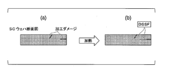
- FIG. 4 It is a schematic cross-sectional schematic diagram of a general SiC single crystal substrate before and after heat treatment.
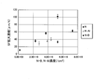
- the horizontal axis represents “donor concentration ⁇ acceptor concentration”, and the vertical axis represents the stacking fault expansion rate.
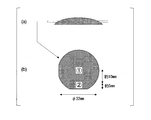
- FIG. 4 A schematic side view of an SiC single crystal ingot manufactured using the method for manufacturing an n-type SiC single crystal substrate of the present invention ((a) of FIG. 4), and manufactured from this ingot and used in Example 1.
- FIG.4 (b) a schematic top view of a 32 mm diameter n-type SiC single crystal substrate.
- FIG. 5 is a table showing the nitrogen concentration, aluminum concentration, and (nitrogen concentration ⁇ aluminum concentration) in the outer peripheral portion and the central portion measured at the position of FIG. 4 in Example 1.
- FIG. 6 shows a resistivity distribution (left graph) measured by the eddy current method, and an estimated (nitrogen concentration-aluminum concentration) distribution (right graph) calculated based on Equation (1) based on the resistivity distribution. ), And a table (lower table) showing (nitrogen concentration-aluminum concentration) of the outer peripheral portion and the central portion measured by SIMS.
- FIG. 1 the cross-sectional schematic diagram of the SiC single crystal substrate before and behind heat processing is shown.
- FIG. 1A is a schematic cross-sectional view of a SiC single crystal substrate before heat treatment.
- FIG. 1B is a schematic cross-sectional view of the SiC single crystal substrate after the heat treatment.
- FIG. 1 (a) it is schematically shown that there is damage (damage) due to beveling on the front side or back side surface and the outer peripheral side surface.
- FIG. 1B it is schematically shown that a double Shockley type stacking fault occurs due to the processing damage after the heat treatment, and expands and enters the device use region. ing.
- the device use area means an area used as a chip, that is, a part excluding a predetermined peripheral vicinity and a part where the chip is actually manufactured.
- the device use area (central part) means an area that is opposite to the edge exclusion area (outer peripheral part) that is not used as a chip, that is, including the central part of the substrate.
- the edge exclusion region a region that is advanced from the outermost periphery (periphery) of the SiC single crystal substrate (wafer) to a predetermined distance toward the center, for example, a substantially donut-shaped region is set.
- an area that extends from the outermost circumference to the center of the wafer up to 2 mm is set as the edge exclusion area, but is not limited thereto.
- the area inside the edge exclusion area is the device use area.
- the “peripheral portion” is a portion (region) where beveling can be performed in the SiC single crystal substrate.
- the “center portion” is a portion (region) closer to the center of the SiC single crystal substrate than the “outer peripheral portion”.
- the “outer periphery” may be a 2 mm portion (region) from the outermost periphery toward the center of the wafer.
- a chip such as a power device is manufactured by processing the device use area. For this reason, it is preferable that the crystallinity of the device use region is good, and it is also desirable that the resistivity is low.
- FIG. 1 shows that a double Shockley type stacking fault occurs in a general SiC single crystal substrate.
- a double Shockley type stacking fault occurs due to damage caused by beveling of the outer peripheral side surface of the SiC single crystal substrate. Then, the defect expands and enters (enters) the device usage area. It is desirable that the double Shockley type stacking fault does not enter the device use area.
- a SiC single crystal is grown by co-doping with a donor and an acceptor on the (000-1) C surface of the seed crystal or a surface having an off angle with respect to this surface by sublimation recrystallization.
- a SiC single crystal ingot is manufactured.
- the crystal growth is performed while keeping the crystal growth surface convex.
- the obtained SiC single crystal ingot is sliced at the C plane or a plane having an off angle with respect to this plane to obtain a SiC single crystal substrate (wafer).
- “donor concentration ⁇ acceptor concentration” in the outer peripheral portion of the wafer becomes smaller than that in the central portion. That is, when the above manufacturing method is performed, the amount (concentration) of nitrogen (N) as a donor is large on the (000-1) C plane (just plane) and decreases when it is deviated from the C plane (just plane). .
- the intake amount (concentration) of aluminum (Al) or boron (B), which is an acceptor does not have such a plane orientation dependency and has a substantially uniform concentration in the plane. The present inventor has found these things. It also made this discovery even better.
- the concentration of nitrogen (donor) is high on the (000-1) C plane (just plane) and decreases when it deviates from the C plane (just plane).
- the concentration of aluminum (Al) or boron (B) has almost no plane orientation dependency in the vicinity of the C plane. Therefore, the “donor concentration-acceptor concentration” in the outer peripheral portion of the SiC single crystal substrate can be made smaller than that in the central portion. When the “donor concentration-acceptor concentration” is low, double Shockley type stacking faults are less likely to occur.
- the “donor concentration-acceptor concentration” degree is low, the expansion rate of the Double Shockley type stacking fault becomes slow. Therefore, it is possible to suppress the introduction of defects from the outer peripheral portion of the SiC single crystal substrate to the device use region during the heat treatment. Note that if the “donor concentration-acceptor concentration” is high in the central portion, an effect that the resistivity decreases in the device use region can be obtained.
- An n-type SiC single crystal substrate is a substrate that has a first main surface, a second main surface (back surface), and an outer peripheral side surface, and is doped with both a donor and an acceptor. Further, the difference between the donor concentration and the acceptor concentration in the outer peripheral portion is smaller than the difference between the donor concentration and the acceptor concentration in the central portion, and the difference between the donor concentration and the acceptor concentration in the outer peripheral portion is 3.0 ⁇ 10 19 / cm 3. Smaller than. It is preferable that the difference between the donor concentration and the acceptor concentration in the outer peripheral portion is smaller than 2.0 ⁇ 10 19 / cm 3 .
- the difference between the donor concentration and the acceptor concentration is preferably larger than 1.0 ⁇ 10 19 / cm 3 in the central portion than in the outer peripheral portion. Since there exists an effect which lowers the resistivity of a center part, it is still more preferable that the center part is larger than 1.4 * 10 ⁇ 19 > / cm ⁇ 3 > rather than an outer peripheral part. In the example shown in FIG. 6, there is a difference in size of about 1.5 ⁇ 10 19 / cm 3 at the maximum.
- the donor concentration and acceptor concentration in the outer peripheral portion, and the donor concentration and acceptor concentration in the central portion can be arbitrarily selected.
- the donor concentration at the outer periphery is preferably 2.0 ⁇ 10 19 to 1.0 ⁇ 10 20 / cm ⁇ 3 , and is preferably 3.0 ⁇ 10 19 to 8.0 ⁇ 10 19 / cm ⁇ 3 . It is more preferable.
- the acceptor concentration at the outer periphery is preferably 0.5 ⁇ 10 19 to 8.0 ⁇ 10 19 / cm ⁇ 3 , and preferably 1.0 ⁇ 10 19 to 6.0 ⁇ 10 19 / cm ⁇ 3. More preferred.
- the donor concentration in the central part is preferably 3.0 ⁇ 10 19 to 1.2 ⁇ 10 20 / cm ⁇ 3 , and preferably 5.0 ⁇ 10 19 to 1.2 ⁇ 10 20 / cm ⁇ 3. More preferred.
- the acceptor concentration at the center is preferably 0.5 ⁇ 10 19 to 8.0 ⁇ 10 19 / cm ⁇ 3 , and preferably 1.0 ⁇ 10 19 to 6.0 ⁇ 10 19 / cm ⁇ 3. More preferred.
- the difference between the donor concentration and the acceptor concentration in the center is preferably 2.0 ⁇ 10 19 to 9.0 ⁇ 10 19 / cm ⁇ 3 , and is 3.0 ⁇ 10 19 to 9.0 ⁇ 10 19 . It is more preferable.
- the n-type SiC single crystal substrate of the present invention is preferably an n-type 4H—SiC single crystal substrate.
- the size and thickness of the substrate may be arbitrarily selected.
- the resistivity of the substrate can also be arbitrarily selected.
- the average resistivity is preferably 1 to 15 m ⁇ ⁇ cm, and more preferably 3 to 10 m ⁇ ⁇ cm.
- any one of group V elements such as nitrogen, phosphorus or arsenic can be preferably used.
- group III elements aluminum, boron or gallium can be preferably used.
- FIG. 2 is a graph obtained by producing a plurality of substrates having the same shape by using nitrogen as a donor and Al or B as an acceptor and using these crystal cross-section samples. Based on the evaluation results of these samples, the horizontal axis represents “donor (N) concentration—acceptor (Al or B) concentration” in the outer peripheral portion, and the vertical axis represents the stacking fault expansion rate.
- a nitrogen-doped sample having the same shape was prepared, evaluated in the same manner, and placed on a graph. In the case of this comparative sample, the horizontal axis indicates the nitrogen concentration.
- this comparative sample was manufactured by the method similar to the method of manufacturing the compound which codoped the nitrogen and boron except having used only nitrogen.
- the “donor (N) concentration—acceptor (Al, B) concentration” of the substrate can be measured by quantitative analysis such as SIMS (secondary ion mass spectrometry).
- “donor (N) concentration ⁇ acceptor (Al, B) concentration” can be derived from the following equation (1) based on resistivity measurement data.
- n Carrier concentration
- ⁇ Resistivity Use measured data
- ⁇ Use mobility assuming 30 (cm 2 / Vs).
- e elementary charge 1.602 ⁇ 10- 19 Coulomb The resistivity was measured by the eddy current method. For the activation rate and mobility, values estimated by hole measurement of crystals having similar carrier concentrations were used.
- the inventors have found that if the “donor concentration-acceptor concentration” in the outer peripheral portion is low, the effect of suppressing the expansion of stacking faults generated when heat treatment is applied to the SiC single crystal substrate (wafer) is found. That is, as shown in FIG. 2, the “donor concentration-acceptor” obtained as the value of the outer peripheral portion of the substrate after the heat treatment in an experiment comparing the case of single doping with nitrogen and the case of doping with two types It has been found that as the “concentration” increases, the difference in the stacking fault expansion rate increases. Conventionally, it has been known that co-doping suppresses the occurrence of stacking faults during the growth of a SiC single crystal (ingot).
- the stacking fault expansion rate shown in FIG. 2 was obtained by the following method. First, an indentation is formed by a micro hardness tester. The dent is taken as the starting point of the stacking fault. Thereafter, the SiC single crystal substrate (wafer) having a recess is heated at 1000 ° C. for 2 hours in an argon atmosphere. Thereafter, molten KOH etching is performed at 500 ° C. for 3 to 5 minutes. This formed etch pits for stacking faults. The distance from the start point to the end of the etch pit was measured using an optical microscope. By dividing this distance by 2 hours, which is the heating time, an expansion rate of stacking faults was obtained. A method for manufacturing the substrate used in FIG. 2 will be described later.
- the nitrogen concentration at which stacking faults increase and the crystallinity is remarkably lowered is a value higher than 2 ⁇ 10 19 / cm 3 .
- the expansion rate of stacking faults at this nitrogen concentration corresponds to about 30 ⁇ m / h. Seem.
- the nitrogen concentration is such that the expansion rate of stacking faults exceeds about 30 ⁇ m / h, stacking faults increase and crystallinity is significantly reduced.
- the stacking fault expansion rate does not exceed 30 ⁇ m / h.
- the “donor concentration-acceptor concentration” at a stacking fault expansion rate of 30 ⁇ m / h is a critical value (critical concentration) indicating whether the stacking fault increases and crystallinity is significantly reduced.
- critical concentration critical concentration
- the concentration is 3.0 ⁇ 10 19 / cm 3 . Therefore, in the n-type SiC single crystal substrate of the present invention, the difference between the donor concentration and the acceptor concentration in the outer peripheral portion is set to be smaller than 3.0 ⁇ 10 19 / cm 3 . More preferably, the difference between the donor concentration and the acceptor concentration at the outer peripheral portion is smaller than 2.0 ⁇ 10 19 / cm 3 .
- a method for producing an SiC single crystal substrate which is a sample obtained from the data shown in FIG. 2, will be described.
- the following method can be preferably used for the production of the substrate.
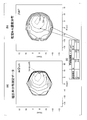
- FIG. 3 is a schematic cross-sectional view showing an example of a SiC single crystal manufacturing apparatus for manufacturing a SiC single crystal substrate.
- the SiC single crystal manufacturing apparatus 10 includes a crucible 1 that forms a reaction space R, a holding unit 2 that can hold a SiC raw material M1, a support unit 3 that supports the holding unit 2, and an installation unit 4 that can install a seed crystal S.
- an aluminum raw material M2 can be installed at the bottom of the crucible 1.
- the seed crystal is preferably a 4H—SiC crystal and is installed in the installation part 4 so that the (000-1) C plane is the growth plane.
- SiC raw material M1 and aluminum raw material M2 are prepared.
- SiC raw material M1 can use SiC powder etc. which are generally used widely.
- the aluminum raw material M2 may be either a nitrided aluminum compound or a non-nitrided aluminum compound.
- the nitrided aluminum compound include aluminum nitride, a compound of aluminum nitride and aluminum carbide, and examples of the non-nitrided aluminum compound include aluminum carbide.
- SiC raw material M1 and aluminum raw material M2 are installed separately, respectively, it is not limited to this.
- the SiC raw material M ⁇ b> 1 can be installed in the holding unit 2, and the aluminum raw material M ⁇ b> 2 can be installed in the bottom of the crucible 1.
- the SiC raw material M1 and the aluminum raw material M2 are sublimated. It is preferable that the SiC raw material M1 and the aluminum raw material M2 are sublimated at different temperatures.
- the vapor pressure of the SiC raw material M1 is lower than the vapor pressure of the aluminum raw material M2. Therefore, when the aluminum raw material M2 is heated under the condition that the normal SiC raw material M1 is sublimated, the aluminum raw material M2 has a large sublimation rate, which causes problems in adjusting the doping amount of aluminum and in growing SiC crystals.
- Control of different temperatures of the SiC raw material M1 and the aluminum raw material M2 can be realized by using the first coil (heater) 5 and the second coil (heater) 6.
- the first coil 5 is designed to heat the first region where the SiC raw material M1 in the crucible 1 exists
- the second coil 6 is designed to heat the second region where the aluminum raw material M2 in the crucible 1 exists.
- the temperature of SiC raw material M1 and aluminum raw material M2 can be controlled separately. More specifically, the temperature is set to about 2200 to 2500 ° C. at which the SiC raw material M1 can be sublimated by the first coil 5, and the temperature is set to about 1700 to 2000 ° C. at which the aluminum raw material M2 can be sublimated by the second coil 6. preferable.
- three samples having different N—Al concentrations were produced by changing the temperature of the aluminum raw material portion M2.
- Nitrogen gas is supplied into the reaction space R.
- Nitrogen gas can be supplied through the crucible 1.
- the crucible 1 can have nitrogen gas permeability. In that case, the nitrogen gas can be supplied into the reaction space R by setting the atmosphere surrounding the crucible 1 to an atmosphere in which nitrogen gas is mixed without providing a gas supply unit in the crucible 1.
- Such a method can provide an ingot suitable for obtaining a desired n-type 4H—SiC single crystal substrate.
- FIG. Each of the three samples having different N—Al concentrations shown in FIG. 2 was manufactured with the growth surface made convex by making the temperature of the center of the seed crystal lower than that of the outer periphery of the seed crystal.
- boron carbide (B 4 C) that can be used as a boron raw material is about three orders of magnitude lower than the vapor pressure of aluminum carbide (Al 4 C 3 ). Therefore, the boron carbide powder can be heated with the same heater as the SiC raw material powder.
- an n-type 4H—SiC single crystal substrate co-doped with nitrogen (N) and boron (B) is the same as an apparatus for producing an n-type 4H—SiC single crystal substrate doped with nitrogen alone.
- a SiC single crystal manufacturing apparatus can be used (for example, refer nonpatent literature 4).
- the boron carbide powder and the SiC raw material powder can be mixed and used. By mixing boron carbide powder and SiC raw material powder, a SiC single crystal in which nitrogen and boron are co-doped is produced using a normal manufacturing method that uses nitrogen alone and a similar SiC single crystal manufacturing process. it can.
- the seed crystal is a 4H—SiC crystal, and is preferably placed so that the (000-1) C plane is the growth plane.
- the temperature of the seed crystal can be set so that the temperature is arbitrarily selected, for example, 2100 ° C. to 2150 ° C.
- the proportion of the B 4 C powder in the raw material powder can be, for example, about 0.001 to 0.1 wt%.
- the temperature can be set so that the raw material powder of the SiC powder and the B 4 C powder has a temperature of 2250 ° C. to 2300 ° C., for example.
- the atmosphere surrounding the crucible is, for example, an atmosphere of argon and nitrogen, and the partial pressure of nitrogen can be set to 5 to 100%, for example.
- FIG. 2 When the NB compound used in the experiment of FIG. 2 was produced, the proportion of B 4 C powder was 0.05 wt%, and the atmosphere surrounding the crucible was an atmosphere of argon and nitrogen. Moreover, the growth surface was made convex by making the temperature of the center part of the seed crystal lower than the peripheral part of the seed crystal. Furthermore, as shown in FIG. 2, three samples with different NB concentrations were produced by changing the flow ratio of nitrogen and argon. The three samples have a difference between the donor concentration and the acceptor concentration at the outer peripheral portion smaller than the difference between the donor concentration and the acceptor concentration at the central portion.
- a manufacturing method of an n-type SiC single crystal substrate according to an embodiment of the present invention includes a crystal growth step of laminating a SiC single crystal while co-doping a donor and an acceptor on one surface of a seed crystal by a sublimation recrystallization method. Have In at least a part of the crystal growth step, the crystal growth surface is maintained in a convex shape. The reason why the crystal growth surface is maintained in a convex shape during the crystal growth process is that the donor concentration is large on the (000-1) C surface (just surface) and decreases when it is deviated from the C surface (just surface). , Surface orientation dependence.
- the acceptor concentration has almost no plane orientation dependency in the vicinity of the C plane. Therefore, the “donor concentration-acceptor concentration” in the outer peripheral portion of the SiC single crystal substrate can be made smaller than that in the central portion.
- the “donor concentration-acceptor concentration” is low, double Shockley type stacking faults are less likely to occur. For example, even if a double Shockley-type stacking fault occurs, if the “donor concentration ⁇ acceptor concentration” is low, the double-Shockley-type stacking fault enlargement rate becomes slow. Therefore, the above feature is preferable because, during the heat treatment, it is possible to suppress the introduction of defects from the outer peripheral portion of the SiC single crystal substrate to the device use region.
- a SiC single crystal ingot may be obtained by the crystal growth step.
- the n-type SiC single crystal substrate of the present invention may be obtained by slicing a substrate from the ingot and performing bering processing or the like on the outer peripheral portion of the sliced substrate.
- the n-type SiC single crystal substrate of the present invention can be preferably manufactured.
- an arbitrary method may be selected. For example, it is also preferable to perform crystal growth in an environment where the temperature of the center portion of the seed crystal is lower than that of the outer periphery of the seed crystal.
- the heating temperature can be set so that the seed crystal has an arbitrarily selected temperature, for example, 2100 to 2150 ° C.
- the seed crystal outer peripheral portion may mean, for example, a region of 5 mm from the outermost periphery to the central direction. The others are used as the center of the seed crystal.
- the temperature difference between the center of the seed crystal and the outer periphery of the seed crystal can be arbitrarily set, but is preferably 1 to 50 ° C., for example, and preferably 2 to 10 ° C.
- the crystal growth rate is fast in the central portion where the temperature is low, and the crystal growth rate is slow in the outer peripheral portion where the temperature is high. For this reason, by setting it as such temperature distribution, a crystal growth surface can be made into an appropriate convex shape. Note that if the temperature distribution in the crystal is increased, a steeper convex shape can be formed, but if the temperature distribution is too large, thermal stress increases, causing cracks and cracks in the crystal and an increase in basal plane dislocations. sell.
- the n-type SiC single crystal substrate of the present invention is manufactured, that is, a known method or condition (such as manufacturing the difference between the donor concentration and the acceptor concentration in the outer peripheral portion smaller than 3.0 ⁇ 10 19 / cm 3 ( For example, see Non-Patent Document 5).
- a known method or condition can be used as a method or condition for controlling the temperature environment of the seed crystal center part and the seed crystal outer peripheral part in which the crystal growth surface has an appropriate convex shape.
- known methods and conditions can be used as methods and conditions for setting appropriate donor concentrations and acceptor concentrations.
- maintaining the crystal growth surface in a convex shape at least in part may mean, for example, that the crystal growth surface has a portion protruding as a curved surface toward the lower side (reaction space side).
- the curvature radius of a convex-shaped part and the size of a bottom face can be selected arbitrarily.
- a heat load step of 1000 ° C. or more and 2000 ° C. or less may be performed after the crystal growth step. Even when such a heat load step is performed, the stacking fault density of the n-type SiC single crystal substrate is 5 cm ⁇ 1 or less.
- An example of the heat load process may include annealing treatment used for adjusting crystallinity, but is not limited thereto.
- SiC epitaxial wafer The SiC epitaxial wafer according to one embodiment of the present invention is obtained by forming a SiC epitaxial film on the n-type SiC single crystal substrate of the present invention. A known method can be used to form the SiC epitaxial film.
- the stacking fault density of the n-type SiC single crystal substrate used for the SiC epitaxial wafer is preferably 5 cm ⁇ 1 or less.
- the stacking fault density of the n-type SiC single crystal substrate is more preferably 2 cm ⁇ 1 or less, and further preferably 1 cm ⁇ 1 or less.
- Example 1 Using the method for producing an n-type SiC single crystal substrate of the present invention, an n-type SiC single crystal substrate having a diameter of 32 mm shown in FIG. 4 was produced. About the said board
- SIMS secondary ion mass spectrometry
- the following method was performed.
- crystal growth was performed in an environment where the temperature was lower in the center of the seed crystal than in the outer periphery of the seed crystal.
- the crystal growth rate is fast in the central portion where the temperature is low, and the crystal growth rate is slow in the outer peripheral portion where the temperature is high. For this reason, it was possible to make the crystal growth surface into an appropriate convex shape by using such a temperature distribution.
- the donor concentration and the acceptor concentration in the outer peripheral portion are smaller than the difference between the donor concentration and the acceptor concentration in the central portion, and these differences are 3.0 ⁇ 10 19. It was smaller than / cm 3 .
- a method for controlling the temperature environment between the seed crystal central portion and the seed crystal outer peripheral portion so that the crystal growth surface has an appropriate convex shape can also be performed by a known method (see, for example, Non-Patent Document 5).
- FIG. 6 shows the resistivity distribution measured by the eddy current method for the obtained substrate (left graph, FIG. 6A), and the calculation based on the above equation (1) based on the resistivity distribution.
- the (nitrogen concentration-aluminum concentration) distribution (right graph, FIG. 6B) is shown.
- the above equation (1) was used only to estimate the “donor concentration-acceptor concentration” distribution from the measured resistivity distribution.
- the activation rate and the mobility were values estimated by hole measurement of crystals having similar “donor concentration and acceptor concentration”.
- the estimated (nitrogen concentration-aluminum concentration) distribution shown as the right diagram in FIG. 6 (FIG. 6B) is the outer circumference measured by SIMS, shown as the lower diagram in FIG. 6 (FIG. 6C).
- the central part (nitrogen concentration-aluminum concentration) were in good agreement. Based on the resistivity measurement data, the effectiveness of calculating “donor concentration-acceptor concentration” based on the above equation (1) was ensured.
- Example 2 A SiC epitaxial wafer in which a SiC epitaxial film was formed on the n-type SiC single crystal substrate of Example 1 at an epitaxial growth temperature of 1600 ° C. was produced.
- the film thickness of the SiC epitaxial film was 10 ⁇ m, and the nitrogen concentration was 1 ⁇ 10 16 / cm 3 .
- photoluminescence (PL) mapping was performed, no light having a peak wavelength (about 500 nm) of the spectrum of a double Shockley type stacking fault was observed, and it was found that no stacking fault occurred (double Shockley type).
- Stacking fault density is 0 cm ⁇ 1 ).
Landscapes
- Chemical & Material Sciences (AREA)
- Engineering & Computer Science (AREA)
- Organic Chemistry (AREA)
- Metallurgy (AREA)
- Materials Engineering (AREA)
- Crystallography & Structural Chemistry (AREA)
- Microelectronics & Electronic Packaging (AREA)
- Power Engineering (AREA)
- Physics & Mathematics (AREA)
- General Physics & Mathematics (AREA)
- Computer Hardware Design (AREA)
- Condensed Matter Physics & Semiconductors (AREA)
- Ceramic Engineering (AREA)
- Inorganic Chemistry (AREA)
- Thermal Sciences (AREA)
- Crystals, And After-Treatments Of Crystals (AREA)
- Physical Deposition Of Substances That Are Components Of Semiconductor Devices (AREA)
Priority Applications (3)
| Application Number | Priority Date | Filing Date | Title |
|---|---|---|---|
| US16/333,269 US10892334B2 (en) | 2016-09-26 | 2017-09-25 | n-Type SiC single crystal substrate, method for producing same and SiC epitaxial wafer |
| DE112017004799.4T DE112017004799B4 (de) | 2016-09-26 | 2017-09-25 | n-Typ-SiC-Einkristallsubstrat, Verfahren zur Herstellung desselben und SiC-Epitaxiewafer |
| CN201780057496.8A CN109715867B (zh) | 2016-09-26 | 2017-09-25 | n型SiC单晶基板及其制造方法以及SiC外延晶片 |
Applications Claiming Priority (2)
| Application Number | Priority Date | Filing Date | Title |
|---|---|---|---|
| JP2016-186907 | 2016-09-26 | ||
| JP2016186907A JP6757955B2 (ja) | 2016-09-26 | 2016-09-26 | n型SiC単結晶基板及びその製造方法、並びにSiCエピタキシャルウェハ |
Publications (1)
| Publication Number | Publication Date |
|---|---|
| WO2018056438A1 true WO2018056438A1 (ja) | 2018-03-29 |
Family
ID=61690505
Family Applications (1)
| Application Number | Title | Priority Date | Filing Date |
|---|---|---|---|
| PCT/JP2017/034499 WO2018056438A1 (ja) | 2016-09-26 | 2017-09-25 | n型SiC単結晶基板及びその製造方法、並びにSiCエピタキシャルウェハ |
Country Status (5)
| Country | Link |
|---|---|
| US (1) | US10892334B2 (zh) |
| JP (1) | JP6757955B2 (zh) |
| CN (1) | CN109715867B (zh) |
| DE (1) | DE112017004799B4 (zh) |
| WO (1) | WO2018056438A1 (zh) |
Cited By (1)
| Publication number | Priority date | Publication date | Assignee | Title |
|---|---|---|---|---|
| JP2018101650A (ja) * | 2016-12-19 | 2018-06-28 | 国立研究開発法人産業技術総合研究所 | 半導体装置の検査方法および半導体基体 |
Families Citing this family (7)
| Publication number | Priority date | Publication date | Assignee | Title |
|---|---|---|---|---|
| JP7173312B2 (ja) * | 2019-05-16 | 2022-11-16 | 富士電機株式会社 | 半導体装置および半導体装置の製造方法 |
| WO2021025085A1 (ja) * | 2019-08-06 | 2021-02-11 | 学校法人関西学院 | SiC基板、SiCエピタキシャル基板、SiCインゴット及びこれらの製造方法 |
| KR102340110B1 (ko) * | 2019-10-29 | 2021-12-17 | 주식회사 쎄닉 | 탄화규소 잉곳, 웨이퍼 및 이의 제조방법 |
| US20230059737A1 (en) * | 2020-01-29 | 2023-02-23 | Sumitomo Electric Industries, Ltd. | Silicon carbide epitaxial substrate and method of manufacturing silicon carbide semiconductor device |
| CN113981528B (zh) * | 2020-07-27 | 2024-06-21 | 环球晶圆股份有限公司 | 碳化硅晶片的制造方法以及半导体结构 |
| JP7183358B1 (ja) * | 2021-08-04 | 2022-12-05 | 昭和電工株式会社 | SiCエピタキシャルウェハ及びSiCエピタキシャルウェハの製造方法 |
| CN113913930A (zh) * | 2021-09-30 | 2022-01-11 | 瀚天天成电子科技(厦门)有限公司 | 一种具有n型缓冲层的外延结构及其制备方法 |
Citations (7)
| Publication number | Priority date | Publication date | Assignee | Title |
|---|---|---|---|---|
| JP2003073194A (ja) * | 2001-06-22 | 2003-03-12 | Bridgestone Corp | 炭化ケイ素単結晶及びその製造方法 |
| JP2006111478A (ja) * | 2004-10-13 | 2006-04-27 | Nippon Steel Corp | 炭化珪素単結晶インゴット、炭化珪素単結晶ウェハ及びその製造方法 |
| JP2010064918A (ja) * | 2008-09-10 | 2010-03-25 | Showa Denko Kk | 炭化珪素単結晶の製造方法、炭化珪素単結晶ウェーハ及び炭化珪素単結晶半導体パワーデバイス |
| JP2011219297A (ja) * | 2010-04-07 | 2011-11-04 | Nippon Steel Corp | 炭化珪素単結晶基板、炭化珪素エピタキシャルウェハ、及び薄膜エピタキシャルウェハ |
| JP2012031014A (ja) * | 2010-07-30 | 2012-02-16 | Denso Corp | 炭化珪素単結晶およびその製造方法 |
| JP2015030640A (ja) * | 2013-08-02 | 2015-02-16 | 株式会社デンソー | 炭化珪素単結晶 |
| WO2015129876A1 (ja) * | 2014-02-27 | 2015-09-03 | 京セラ株式会社 | 炭化珪素の結晶のインゴット、炭化珪素のウェハ、炭化珪素の結晶のインゴットおよび炭化珪素のウェハの製造方法 |
Family Cites Families (8)
| Publication number | Priority date | Publication date | Assignee | Title |
|---|---|---|---|---|
| US20020189536A1 (en) | 2001-06-15 | 2002-12-19 | Bridgestone Corporation | Silicon carbide single crystal and production thereof |
| JP4964672B2 (ja) | 2007-05-23 | 2012-07-04 | 新日本製鐵株式会社 | 低抵抗率炭化珪素単結晶基板 |
| JP4469396B2 (ja) * | 2008-01-15 | 2010-05-26 | 新日本製鐵株式会社 | 炭化珪素単結晶インゴット、これから得られる基板及びエピタキシャルウェハ |
| JP4697235B2 (ja) * | 2008-01-29 | 2011-06-08 | トヨタ自動車株式会社 | p型SiC半導体単結晶の製造方法およびそれにより製造されたp型SiC半導体単結晶 |
| CN102245813B (zh) * | 2008-12-08 | 2014-08-06 | Ii-Vi有限公司 | 改进的轴向梯度传输(agt)生长工艺和利用电阻加热的装置 |
| JP2011093771A (ja) * | 2009-11-02 | 2011-05-12 | Bridgestone Corp | 炭化ケイ素単結晶、炭化ケイ素単結晶基板、および炭化ケイ素単結晶の製造方法 |
| JP2014187113A (ja) * | 2013-03-22 | 2014-10-02 | Toshiba Corp | 気相成長装置および気相成長方法 |
| JP2016186907A (ja) | 2015-03-27 | 2016-10-27 | 三菱製紙株式会社 | 導電性材料の製造方法 |
-
2016
- 2016-09-26 JP JP2016186907A patent/JP6757955B2/ja active Active
-
2017
- 2017-09-25 US US16/333,269 patent/US10892334B2/en active Active
- 2017-09-25 CN CN201780057496.8A patent/CN109715867B/zh active Active
- 2017-09-25 WO PCT/JP2017/034499 patent/WO2018056438A1/ja active Application Filing
- 2017-09-25 DE DE112017004799.4T patent/DE112017004799B4/de active Active
Patent Citations (7)
| Publication number | Priority date | Publication date | Assignee | Title |
|---|---|---|---|---|
| JP2003073194A (ja) * | 2001-06-22 | 2003-03-12 | Bridgestone Corp | 炭化ケイ素単結晶及びその製造方法 |
| JP2006111478A (ja) * | 2004-10-13 | 2006-04-27 | Nippon Steel Corp | 炭化珪素単結晶インゴット、炭化珪素単結晶ウェハ及びその製造方法 |
| JP2010064918A (ja) * | 2008-09-10 | 2010-03-25 | Showa Denko Kk | 炭化珪素単結晶の製造方法、炭化珪素単結晶ウェーハ及び炭化珪素単結晶半導体パワーデバイス |
| JP2011219297A (ja) * | 2010-04-07 | 2011-11-04 | Nippon Steel Corp | 炭化珪素単結晶基板、炭化珪素エピタキシャルウェハ、及び薄膜エピタキシャルウェハ |
| JP2012031014A (ja) * | 2010-07-30 | 2012-02-16 | Denso Corp | 炭化珪素単結晶およびその製造方法 |
| JP2015030640A (ja) * | 2013-08-02 | 2015-02-16 | 株式会社デンソー | 炭化珪素単結晶 |
| WO2015129876A1 (ja) * | 2014-02-27 | 2015-09-03 | 京セラ株式会社 | 炭化珪素の結晶のインゴット、炭化珪素のウェハ、炭化珪素の結晶のインゴットおよび炭化珪素のウェハの製造方法 |
Cited By (1)
| Publication number | Priority date | Publication date | Assignee | Title |
|---|---|---|---|---|
| JP2018101650A (ja) * | 2016-12-19 | 2018-06-28 | 国立研究開発法人産業技術総合研究所 | 半導体装置の検査方法および半導体基体 |
Also Published As
| Publication number | Publication date |
|---|---|
| CN109715867A (zh) | 2019-05-03 |
| US10892334B2 (en) | 2021-01-12 |
| JP2018052749A (ja) | 2018-04-05 |
| DE112017004799B4 (de) | 2022-06-30 |
| JP6757955B2 (ja) | 2020-09-23 |
| US20190252504A1 (en) | 2019-08-15 |
| DE112017004799T5 (de) | 2019-09-05 |
| CN109715867B (zh) | 2021-06-22 |
Similar Documents
| Publication | Publication Date | Title |
|---|---|---|
| WO2018056438A1 (ja) | n型SiC単結晶基板及びその製造方法、並びにSiCエピタキシャルウェハ | |
| JP6755524B2 (ja) | p型4H−SiC単結晶及びp型4H−SiC単結晶の製造方法 | |
| JP5706823B2 (ja) | SiC単結晶ウエハーとその製造方法 | |
| JP5304713B2 (ja) | 炭化珪素単結晶基板、炭化珪素エピタキシャルウェハ、及び薄膜エピタキシャルウェハ | |
| WO2011142470A1 (ja) | エピタキシャル炭化珪素単結晶基板及びその製造方法 | |
| JP2006111478A (ja) | 炭化珪素単結晶インゴット、炭化珪素単結晶ウェハ及びその製造方法 | |
| JP2008290898A (ja) | 低抵抗率炭化珪素単結晶基板 | |
| US20140054609A1 (en) | Large high-quality epitaxial wafers | |
| JP2008053343A (ja) | 炭化珪素半導体エピタキシャル基板の製造方法 | |
| JP2006328455A (ja) | エピタキシャル炭化珪素単結晶基板及びその製造方法 | |
| JP6624868B2 (ja) | p型低抵抗率炭化珪素単結晶基板 | |
| JP4442366B2 (ja) | エピタキシャルSiC膜とその製造方法およびSiC半導体デバイス | |
| JP2017065986A (ja) | 低抵抗率炭化珪素単結晶基板の製造方法 | |
| CN110663099B (zh) | SiC外延晶片及其制造方法 | |
| JP2020033230A (ja) | n型4H−SiC単結晶基板およびn型4H−SiC単結晶基板の製造方法 | |
| JP2006001784A (ja) | 炭化珪素単結晶および単結晶ウェハ | |
| US11948794B2 (en) | Method of manufacturing silicon carbide epitaxial wafer | |
| US10329689B2 (en) | Silicon carbide epitaxial wafer and process for producing same | |
| WO2020059810A1 (ja) | デバイス作製用ウエハの製造方法 | |
| US20220310795A1 (en) | Silicon carbide epitaxial substrate and method for manufacturing same | |
| JP2024522507A (ja) | シリコンカーバイド結晶性材料のための光吸収の低減 | |
| JP2010278208A (ja) | 炭化シリコン膜の製造方法 | |
| JP2017082317A (ja) | 新規な積層体 |
Legal Events
| Date | Code | Title | Description |
|---|---|---|---|
| 121 | Ep: the epo has been informed by wipo that ep was designated in this application |
Ref document number: 17853205 Country of ref document: EP Kind code of ref document: A1 |
|
| 122 | Ep: pct application non-entry in european phase |
Ref document number: 17853205 Country of ref document: EP Kind code of ref document: A1 |