WO2018055902A1 - 表示装置及び電子機器 - Google Patents
表示装置及び電子機器 Download PDFInfo
- Publication number
- WO2018055902A1 WO2018055902A1 PCT/JP2017/027160 JP2017027160W WO2018055902A1 WO 2018055902 A1 WO2018055902 A1 WO 2018055902A1 JP 2017027160 W JP2017027160 W JP 2017027160W WO 2018055902 A1 WO2018055902 A1 WO 2018055902A1
- Authority
- WO
- WIPO (PCT)
- Prior art keywords
- wiring
- wiring layer
- layer
- light emitting
- pixel
- Prior art date
Links
- 239000011159 matrix material Substances 0.000 claims abstract description 21
- 239000003990 capacitor Substances 0.000 claims description 66
- 238000009792 diffusion process Methods 0.000 claims description 22
- 239000010410 layer Substances 0.000 description 376
- 238000000034 method Methods 0.000 description 58
- 239000010408 film Substances 0.000 description 52
- 239000000463 material Substances 0.000 description 44
- 239000000758 substrate Substances 0.000 description 44
- 239000012212 insulator Substances 0.000 description 32
- 239000012044 organic layer Substances 0.000 description 27
- 238000005070 sampling Methods 0.000 description 24
- 238000010586 diagram Methods 0.000 description 22
- 238000012937 correction Methods 0.000 description 20
- 239000011229 interlayer Substances 0.000 description 15
- 230000000694 effects Effects 0.000 description 12
- 230000001681 protective effect Effects 0.000 description 11
- 229910004298 SiO 2 Inorganic materials 0.000 description 10
- 229910045601 alloy Inorganic materials 0.000 description 10
- 239000000956 alloy Substances 0.000 description 10
- 229910052782 aluminium Inorganic materials 0.000 description 10
- XAGFODPZIPBFFR-UHFFFAOYSA-N aluminium Chemical compound [Al] XAGFODPZIPBFFR-UHFFFAOYSA-N 0.000 description 10
- 239000008186 active pharmaceutical agent Substances 0.000 description 8
- BQCADISMDOOEFD-UHFFFAOYSA-N Silver Chemical compound [Ag] BQCADISMDOOEFD-UHFFFAOYSA-N 0.000 description 7
- 238000005229 chemical vapour deposition Methods 0.000 description 7
- 238000005530 etching Methods 0.000 description 7
- 229910052709 silver Inorganic materials 0.000 description 7
- 239000004332 silver Substances 0.000 description 7
- 239000004020 conductor Substances 0.000 description 6
- 230000006866 deterioration Effects 0.000 description 6
- 238000007667 floating Methods 0.000 description 6
- 239000011521 glass Substances 0.000 description 6
- 238000001771 vacuum deposition Methods 0.000 description 6
- 239000003086 colorant Substances 0.000 description 5
- 230000007547 defect Effects 0.000 description 5
- 238000002347 injection Methods 0.000 description 5
- 239000007924 injection Substances 0.000 description 5
- 238000000059 patterning Methods 0.000 description 5
- 238000002360 preparation method Methods 0.000 description 5
- 239000004065 semiconductor Substances 0.000 description 5
- 239000011734 sodium Substances 0.000 description 5
- 238000003860 storage Methods 0.000 description 5
- VYPSYNLAJGMNEJ-UHFFFAOYSA-N Silicium dioxide Chemical compound O=[Si]=O VYPSYNLAJGMNEJ-UHFFFAOYSA-N 0.000 description 4
- 230000008859 change Effects 0.000 description 4
- 239000010949 copper Substances 0.000 description 4
- 238000000151 deposition Methods 0.000 description 4
- 238000013461 design Methods 0.000 description 4
- 238000000605 extraction Methods 0.000 description 4
- 239000011777 magnesium Substances 0.000 description 4
- 229910052751 metal Inorganic materials 0.000 description 4
- 239000002184 metal Substances 0.000 description 4
- 238000000206 photolithography Methods 0.000 description 4
- 229920000642 polymer Polymers 0.000 description 4
- 238000007639 printing Methods 0.000 description 4
- 239000011347 resin Substances 0.000 description 4
- 229920005989 resin Polymers 0.000 description 4
- 230000004044 response Effects 0.000 description 4
- 229910052814 silicon oxide Inorganic materials 0.000 description 4
- RYGMFSIKBFXOCR-UHFFFAOYSA-N Copper Chemical compound [Cu] RYGMFSIKBFXOCR-UHFFFAOYSA-N 0.000 description 3
- PXHVJJICTQNCMI-UHFFFAOYSA-N Nickel Chemical compound [Ni] PXHVJJICTQNCMI-UHFFFAOYSA-N 0.000 description 3
- KDLHZDBZIXYQEI-UHFFFAOYSA-N Palladium Chemical compound [Pd] KDLHZDBZIXYQEI-UHFFFAOYSA-N 0.000 description 3
- 239000011575 calcium Substances 0.000 description 3
- 229910052802 copper Inorganic materials 0.000 description 3
- 239000010931 gold Substances 0.000 description 3
- 230000005525 hole transport Effects 0.000 description 3
- 238000010030 laminating Methods 0.000 description 3
- 229910052749 magnesium Inorganic materials 0.000 description 3
- 238000004519 manufacturing process Methods 0.000 description 3
- 239000000203 mixture Substances 0.000 description 3
- 230000003071 parasitic effect Effects 0.000 description 3
- BASFCYQUMIYNBI-UHFFFAOYSA-N platinum Chemical compound [Pt] BASFCYQUMIYNBI-UHFFFAOYSA-N 0.000 description 3
- 229920003229 poly(methyl methacrylate) Polymers 0.000 description 3
- 229920001721 polyimide Polymers 0.000 description 3
- 239000004926 polymethyl methacrylate Substances 0.000 description 3
- 230000008569 process Effects 0.000 description 3
- 238000007789 sealing Methods 0.000 description 3
- 230000007704 transition Effects 0.000 description 3
- 238000007740 vapor deposition Methods 0.000 description 3
- 239000004925 Acrylic resin Substances 0.000 description 2
- 229920000178 Acrylic resin Polymers 0.000 description 2
- 229910001316 Ag alloy Inorganic materials 0.000 description 2
- 229910000882 Ca alloy Inorganic materials 0.000 description 2
- OYPRJOBELJOOCE-UHFFFAOYSA-N Calcium Chemical compound [Ca] OYPRJOBELJOOCE-UHFFFAOYSA-N 0.000 description 2
- FYYHWMGAXLPEAU-UHFFFAOYSA-N Magnesium Chemical compound [Mg] FYYHWMGAXLPEAU-UHFFFAOYSA-N 0.000 description 2
- 229910000861 Mg alloy Inorganic materials 0.000 description 2
- 229910019015 Mg-Ag Inorganic materials 0.000 description 2
- 229910000583 Nd alloy Inorganic materials 0.000 description 2
- 229920001665 Poly-4-vinylphenol Polymers 0.000 description 2
- 239000004372 Polyvinyl alcohol Substances 0.000 description 2
- HCHKCACWOHOZIP-UHFFFAOYSA-N Zinc Chemical compound [Zn] HCHKCACWOHOZIP-UHFFFAOYSA-N 0.000 description 2
- 238000010521 absorption reaction Methods 0.000 description 2
- 230000008033 biological extinction Effects 0.000 description 2
- 239000011651 chromium Substances 0.000 description 2
- 238000000576 coating method Methods 0.000 description 2
- 230000006835 compression Effects 0.000 description 2
- 238000007906 compression Methods 0.000 description 2
- PCHJSUWPFVWCPO-UHFFFAOYSA-N gold Chemical compound [Au] PCHJSUWPFVWCPO-UHFFFAOYSA-N 0.000 description 2
- 229910052737 gold Inorganic materials 0.000 description 2
- 229910052738 indium Inorganic materials 0.000 description 2
- APFVFJFRJDLVQX-UHFFFAOYSA-N indium atom Chemical compound [In] APFVFJFRJDLVQX-UHFFFAOYSA-N 0.000 description 2
- 238000007641 inkjet printing Methods 0.000 description 2
- 230000001151 other effect Effects 0.000 description 2
- 238000005240 physical vapour deposition Methods 0.000 description 2
- 229920000139 polyethylene terephthalate Polymers 0.000 description 2
- 239000005020 polyethylene terephthalate Substances 0.000 description 2
- 239000009719 polyimide resin Substances 0.000 description 2
- 229920002451 polyvinyl alcohol Polymers 0.000 description 2
- 230000000644 propagated effect Effects 0.000 description 2
- 239000010453 quartz Substances 0.000 description 2
- 238000007650 screen-printing Methods 0.000 description 2
- 238000004544 sputter deposition Methods 0.000 description 2
- 239000013589 supplement Substances 0.000 description 2
- 238000012546 transfer Methods 0.000 description 2
- WFKWXMTUELFFGS-UHFFFAOYSA-N tungsten Chemical compound [W] WFKWXMTUELFFGS-UHFFFAOYSA-N 0.000 description 2
- 229910052721 tungsten Inorganic materials 0.000 description 2
- 239000010937 tungsten Substances 0.000 description 2
- 229910000838 Al alloy Inorganic materials 0.000 description 1
- 229910001148 Al-Li alloy Inorganic materials 0.000 description 1
- 229910001020 Au alloy Inorganic materials 0.000 description 1
- WKBOTKDWSSQWDR-UHFFFAOYSA-N Bromine atom Chemical compound [Br] WKBOTKDWSSQWDR-UHFFFAOYSA-N 0.000 description 1
- VYZAMTAEIAYCRO-UHFFFAOYSA-N Chromium Chemical compound [Cr] VYZAMTAEIAYCRO-UHFFFAOYSA-N 0.000 description 1
- 229910000881 Cu alloy Inorganic materials 0.000 description 1
- DGAQECJNVWCQMB-PUAWFVPOSA-M Ilexoside XXIX Chemical compound C[C@@H]1CC[C@@]2(CC[C@@]3(C(=CC[C@H]4[C@]3(CC[C@@H]5[C@@]4(CC[C@@H](C5(C)C)OS(=O)(=O)[O-])C)C)[C@@H]2[C@]1(C)O)C)C(=O)O[C@H]6[C@@H]([C@H]([C@@H]([C@H](O6)CO)O)O)O.[Na+] DGAQECJNVWCQMB-PUAWFVPOSA-M 0.000 description 1
- XEEYBQQBJWHFJM-UHFFFAOYSA-N Iron Chemical compound [Fe] XEEYBQQBJWHFJM-UHFFFAOYSA-N 0.000 description 1
- WHXSMMKQMYFTQS-UHFFFAOYSA-N Lithium Chemical compound [Li] WHXSMMKQMYFTQS-UHFFFAOYSA-N 0.000 description 1
- 229910052779 Neodymium Inorganic materials 0.000 description 1
- 229910002668 Pd-Cu Inorganic materials 0.000 description 1
- 229920012266 Poly(ether sulfone) PES Polymers 0.000 description 1
- 239000004642 Polyimide Substances 0.000 description 1
- 229910004283 SiO 4 Inorganic materials 0.000 description 1
- XUIMIQQOPSSXEZ-UHFFFAOYSA-N Silicon Chemical compound [Si] XUIMIQQOPSSXEZ-UHFFFAOYSA-N 0.000 description 1
- CDBYLPFSWZWCQE-UHFFFAOYSA-L Sodium Carbonate Chemical compound [Na+].[Na+].[O-]C([O-])=O CDBYLPFSWZWCQE-UHFFFAOYSA-L 0.000 description 1
- NINIDFKCEFEMDL-UHFFFAOYSA-N Sulfur Chemical compound [S] NINIDFKCEFEMDL-UHFFFAOYSA-N 0.000 description 1
- 229910010413 TiO 2 Inorganic materials 0.000 description 1
- ATJFFYVFTNAWJD-UHFFFAOYSA-N Tin Chemical compound [Sn] ATJFFYVFTNAWJD-UHFFFAOYSA-N 0.000 description 1
- RTAQQCXQSZGOHL-UHFFFAOYSA-N Titanium Chemical compound [Ti] RTAQQCXQSZGOHL-UHFFFAOYSA-N 0.000 description 1
- QCWXUUIWCKQGHC-UHFFFAOYSA-N Zirconium Chemical compound [Zr] QCWXUUIWCKQGHC-UHFFFAOYSA-N 0.000 description 1
- 229910052783 alkali metal Inorganic materials 0.000 description 1
- 150000001340 alkali metals Chemical class 0.000 description 1
- 229910052784 alkaline earth metal Inorganic materials 0.000 description 1
- 150000001342 alkaline earth metals Chemical class 0.000 description 1
- 230000005540 biological transmission Effects 0.000 description 1
- 239000005380 borophosphosilicate glass Substances 0.000 description 1
- 239000005388 borosilicate glass Substances 0.000 description 1
- GDTBXPJZTBHREO-UHFFFAOYSA-N bromine Substances BrBr GDTBXPJZTBHREO-UHFFFAOYSA-N 0.000 description 1
- 229910052794 bromium Inorganic materials 0.000 description 1
- QHIWVLPBUQWDMQ-UHFFFAOYSA-N butyl prop-2-enoate;methyl 2-methylprop-2-enoate;prop-2-enoic acid Chemical compound OC(=O)C=C.COC(=O)C(C)=C.CCCCOC(=O)C=C QHIWVLPBUQWDMQ-UHFFFAOYSA-N 0.000 description 1
- 229910052791 calcium Inorganic materials 0.000 description 1
- 229910052804 chromium Inorganic materials 0.000 description 1
- 229910017052 cobalt Inorganic materials 0.000 description 1
- 239000010941 cobalt Substances 0.000 description 1
- GUTLYIVDDKVIGB-UHFFFAOYSA-N cobalt atom Chemical compound [Co] GUTLYIVDDKVIGB-UHFFFAOYSA-N 0.000 description 1
- 230000000295 complement effect Effects 0.000 description 1
- 239000000470 constituent Substances 0.000 description 1
- 230000007423 decrease Effects 0.000 description 1
- 238000007772 electroless plating Methods 0.000 description 1
- 238000005401 electroluminescence Methods 0.000 description 1
- 238000010894 electron beam technology Methods 0.000 description 1
- 238000009713 electroplating Methods 0.000 description 1
- 238000005516 engineering process Methods 0.000 description 1
- 239000003822 epoxy resin Substances 0.000 description 1
- 239000004811 fluoropolymer Substances 0.000 description 1
- 229920002313 fluoropolymer Polymers 0.000 description 1
- 229910052839 forsterite Inorganic materials 0.000 description 1
- 239000003353 gold alloy Substances 0.000 description 1
- 238000004050 hot filament vapor deposition Methods 0.000 description 1
- 238000007733 ion plating Methods 0.000 description 1
- 230000001678 irradiating effect Effects 0.000 description 1
- 238000000608 laser ablation Methods 0.000 description 1
- 239000005355 lead glass Substances 0.000 description 1
- 229910052744 lithium Inorganic materials 0.000 description 1
- HCWCAKKEBCNQJP-UHFFFAOYSA-N magnesium orthosilicate Chemical compound [Mg+2].[Mg+2].[O-][Si]([O-])([O-])[O-] HCWCAKKEBCNQJP-UHFFFAOYSA-N 0.000 description 1
- 230000014759 maintenance of location Effects 0.000 description 1
- 230000008018 melting Effects 0.000 description 1
- 238000002844 melting Methods 0.000 description 1
- 238000002488 metal-organic chemical vapour deposition Methods 0.000 description 1
- 238000012986 modification Methods 0.000 description 1
- 230000004048 modification Effects 0.000 description 1
- QEFYFXOXNSNQGX-UHFFFAOYSA-N neodymium atom Chemical compound [Nd] QEFYFXOXNSNQGX-UHFFFAOYSA-N 0.000 description 1
- 229910052759 nickel Inorganic materials 0.000 description 1
- 229920003986 novolac Polymers 0.000 description 1
- 238000001579 optical reflectometry Methods 0.000 description 1
- 239000011368 organic material Substances 0.000 description 1
- 229920000620 organic polymer Polymers 0.000 description 1
- 229910052763 palladium Inorganic materials 0.000 description 1
- 238000007747 plating Methods 0.000 description 1
- 229910052697 platinum Inorganic materials 0.000 description 1
- 238000005498 polishing Methods 0.000 description 1
- 229920002577 polybenzoxazole Polymers 0.000 description 1
- 229920000515 polycarbonate Polymers 0.000 description 1
- 239000004417 polycarbonate Substances 0.000 description 1
- 229920000647 polyepoxide Polymers 0.000 description 1
- -1 polyethylene terephthalate Polymers 0.000 description 1
- 238000010791 quenching Methods 0.000 description 1
- 230000000171 quenching effect Effects 0.000 description 1
- 229910052710 silicon Inorganic materials 0.000 description 1
- 239000010703 silicon Substances 0.000 description 1
- 229920005573 silicon-containing polymer Polymers 0.000 description 1
- 229920002050 silicone resin Polymers 0.000 description 1
- 238000004088 simulation Methods 0.000 description 1
- 239000002356 single layer Substances 0.000 description 1
- 229910052708 sodium Inorganic materials 0.000 description 1
- 238000003980 solgel method Methods 0.000 description 1
- 229910052712 strontium Inorganic materials 0.000 description 1
- CIOAGBVUUVVLOB-UHFFFAOYSA-N strontium atom Chemical compound [Sr] CIOAGBVUUVVLOB-UHFFFAOYSA-N 0.000 description 1
- 239000000126 substance Substances 0.000 description 1
- 239000011593 sulfur Substances 0.000 description 1
- 229910052717 sulfur Inorganic materials 0.000 description 1
- 229910052715 tantalum Inorganic materials 0.000 description 1
- GUVRBAGPIYLISA-UHFFFAOYSA-N tantalum atom Chemical compound [Ta] GUVRBAGPIYLISA-UHFFFAOYSA-N 0.000 description 1
- 239000010409 thin film Substances 0.000 description 1
- 239000010936 titanium Substances 0.000 description 1
- 229910052719 titanium Inorganic materials 0.000 description 1
- 238000002834 transmittance Methods 0.000 description 1
- 229910052725 zinc Inorganic materials 0.000 description 1
- 239000011701 zinc Substances 0.000 description 1
- 229910052726 zirconium Inorganic materials 0.000 description 1
Images


Classifications
-
- H—ELECTRICITY
- H10—SEMICONDUCTOR DEVICES; ELECTRIC SOLID-STATE DEVICES NOT OTHERWISE PROVIDED FOR
- H10K—ORGANIC ELECTRIC SOLID-STATE DEVICES
- H10K59/00—Integrated devices, or assemblies of multiple devices, comprising at least one organic light-emitting element covered by group H10K50/00
- H10K59/10—OLED displays
- H10K59/12—Active-matrix OLED [AMOLED] displays
-
- H—ELECTRICITY
- H01—ELECTRIC ELEMENTS
- H01L—SEMICONDUCTOR DEVICES NOT COVERED BY CLASS H10
- H01L27/00—Devices consisting of a plurality of semiconductor or other solid-state components formed in or on a common substrate
- H01L27/02—Devices consisting of a plurality of semiconductor or other solid-state components formed in or on a common substrate including semiconductor components specially adapted for rectifying, oscillating, amplifying or switching and having potential barriers; including integrated passive circuit elements having potential barriers
- H01L27/12—Devices consisting of a plurality of semiconductor or other solid-state components formed in or on a common substrate including semiconductor components specially adapted for rectifying, oscillating, amplifying or switching and having potential barriers; including integrated passive circuit elements having potential barriers the substrate being other than a semiconductor body, e.g. an insulating body
- H01L27/1214—Devices consisting of a plurality of semiconductor or other solid-state components formed in or on a common substrate including semiconductor components specially adapted for rectifying, oscillating, amplifying or switching and having potential barriers; including integrated passive circuit elements having potential barriers the substrate being other than a semiconductor body, e.g. an insulating body comprising a plurality of TFTs formed on a non-semiconducting substrate, e.g. driving circuits for AMLCDs
- H01L27/124—Devices consisting of a plurality of semiconductor or other solid-state components formed in or on a common substrate including semiconductor components specially adapted for rectifying, oscillating, amplifying or switching and having potential barriers; including integrated passive circuit elements having potential barriers the substrate being other than a semiconductor body, e.g. an insulating body comprising a plurality of TFTs formed on a non-semiconducting substrate, e.g. driving circuits for AMLCDs with a particular composition, shape or layout of the wiring layers specially adapted to the circuit arrangement, e.g. scanning lines in LCD pixel circuits
-
- G—PHYSICS
- G09—EDUCATION; CRYPTOGRAPHY; DISPLAY; ADVERTISING; SEALS
- G09G—ARRANGEMENTS OR CIRCUITS FOR CONTROL OF INDICATING DEVICES USING STATIC MEANS TO PRESENT VARIABLE INFORMATION
- G09G3/00—Control arrangements or circuits, of interest only in connection with visual indicators other than cathode-ray tubes
- G09G3/20—Control arrangements or circuits, of interest only in connection with visual indicators other than cathode-ray tubes for presentation of an assembly of a number of characters, e.g. a page, by composing the assembly by combination of individual elements arranged in a matrix no fixed position being assigned to or needed to be assigned to the individual characters or partial characters
- G09G3/22—Control arrangements or circuits, of interest only in connection with visual indicators other than cathode-ray tubes for presentation of an assembly of a number of characters, e.g. a page, by composing the assembly by combination of individual elements arranged in a matrix no fixed position being assigned to or needed to be assigned to the individual characters or partial characters using controlled light sources
- G09G3/30—Control arrangements or circuits, of interest only in connection with visual indicators other than cathode-ray tubes for presentation of an assembly of a number of characters, e.g. a page, by composing the assembly by combination of individual elements arranged in a matrix no fixed position being assigned to or needed to be assigned to the individual characters or partial characters using controlled light sources using electroluminescent panels
- G09G3/32—Control arrangements or circuits, of interest only in connection with visual indicators other than cathode-ray tubes for presentation of an assembly of a number of characters, e.g. a page, by composing the assembly by combination of individual elements arranged in a matrix no fixed position being assigned to or needed to be assigned to the individual characters or partial characters using controlled light sources using electroluminescent panels semiconductive, e.g. using light-emitting diodes [LED]
- G09G3/3208—Control arrangements or circuits, of interest only in connection with visual indicators other than cathode-ray tubes for presentation of an assembly of a number of characters, e.g. a page, by composing the assembly by combination of individual elements arranged in a matrix no fixed position being assigned to or needed to be assigned to the individual characters or partial characters using controlled light sources using electroluminescent panels semiconductive, e.g. using light-emitting diodes [LED] organic, e.g. using organic light-emitting diodes [OLED]
- G09G3/3266—Details of drivers for scan electrodes
-
- H—ELECTRICITY
- H01—ELECTRIC ELEMENTS
- H01L—SEMICONDUCTOR DEVICES NOT COVERED BY CLASS H10
- H01L27/00—Devices consisting of a plurality of semiconductor or other solid-state components formed in or on a common substrate
- H01L27/02—Devices consisting of a plurality of semiconductor or other solid-state components formed in or on a common substrate including semiconductor components specially adapted for rectifying, oscillating, amplifying or switching and having potential barriers; including integrated passive circuit elements having potential barriers
- H01L27/12—Devices consisting of a plurality of semiconductor or other solid-state components formed in or on a common substrate including semiconductor components specially adapted for rectifying, oscillating, amplifying or switching and having potential barriers; including integrated passive circuit elements having potential barriers the substrate being other than a semiconductor body, e.g. an insulating body
- H01L27/1214—Devices consisting of a plurality of semiconductor or other solid-state components formed in or on a common substrate including semiconductor components specially adapted for rectifying, oscillating, amplifying or switching and having potential barriers; including integrated passive circuit elements having potential barriers the substrate being other than a semiconductor body, e.g. an insulating body comprising a plurality of TFTs formed on a non-semiconducting substrate, e.g. driving circuits for AMLCDs
- H01L27/1255—Devices consisting of a plurality of semiconductor or other solid-state components formed in or on a common substrate including semiconductor components specially adapted for rectifying, oscillating, amplifying or switching and having potential barriers; including integrated passive circuit elements having potential barriers the substrate being other than a semiconductor body, e.g. an insulating body comprising a plurality of TFTs formed on a non-semiconducting substrate, e.g. driving circuits for AMLCDs integrated with passive devices, e.g. auxiliary capacitors
-
- H—ELECTRICITY
- H10—SEMICONDUCTOR DEVICES; ELECTRIC SOLID-STATE DEVICES NOT OTHERWISE PROVIDED FOR
- H10K—ORGANIC ELECTRIC SOLID-STATE DEVICES
- H10K50/00—Organic light-emitting devices
- H10K50/10—OLEDs or polymer light-emitting diodes [PLED]
- H10K50/11—OLEDs or polymer light-emitting diodes [PLED] characterised by the electroluminescent [EL] layers
- H10K50/125—OLEDs or polymer light-emitting diodes [PLED] characterised by the electroluminescent [EL] layers specially adapted for multicolour light emission, e.g. for emitting white light
-
- H—ELECTRICITY
- H10—SEMICONDUCTOR DEVICES; ELECTRIC SOLID-STATE DEVICES NOT OTHERWISE PROVIDED FOR
- H10K—ORGANIC ELECTRIC SOLID-STATE DEVICES
- H10K59/00—Integrated devices, or assemblies of multiple devices, comprising at least one organic light-emitting element covered by group H10K50/00
- H10K59/10—OLED displays
- H10K59/12—Active-matrix OLED [AMOLED] displays
- H10K59/121—Active-matrix OLED [AMOLED] displays characterised by the geometry or disposition of pixel elements
- H10K59/1213—Active-matrix OLED [AMOLED] displays characterised by the geometry or disposition of pixel elements the pixel elements being TFTs
-
- H—ELECTRICITY
- H10—SEMICONDUCTOR DEVICES; ELECTRIC SOLID-STATE DEVICES NOT OTHERWISE PROVIDED FOR
- H10K—ORGANIC ELECTRIC SOLID-STATE DEVICES
- H10K59/00—Integrated devices, or assemblies of multiple devices, comprising at least one organic light-emitting element covered by group H10K50/00
- H10K59/10—OLED displays
- H10K59/12—Active-matrix OLED [AMOLED] displays
- H10K59/121—Active-matrix OLED [AMOLED] displays characterised by the geometry or disposition of pixel elements
- H10K59/1216—Active-matrix OLED [AMOLED] displays characterised by the geometry or disposition of pixel elements the pixel elements being capacitors
-
- H—ELECTRICITY
- H10—SEMICONDUCTOR DEVICES; ELECTRIC SOLID-STATE DEVICES NOT OTHERWISE PROVIDED FOR
- H10K—ORGANIC ELECTRIC SOLID-STATE DEVICES
- H10K59/00—Integrated devices, or assemblies of multiple devices, comprising at least one organic light-emitting element covered by group H10K50/00
- H10K59/10—OLED displays
- H10K59/12—Active-matrix OLED [AMOLED] displays
- H10K59/122—Pixel-defining structures or layers, e.g. banks
-
- H—ELECTRICITY
- H10—SEMICONDUCTOR DEVICES; ELECTRIC SOLID-STATE DEVICES NOT OTHERWISE PROVIDED FOR
- H10K—ORGANIC ELECTRIC SOLID-STATE DEVICES
- H10K59/00—Integrated devices, or assemblies of multiple devices, comprising at least one organic light-emitting element covered by group H10K50/00
- H10K59/10—OLED displays
- H10K59/12—Active-matrix OLED [AMOLED] displays
- H10K59/131—Interconnections, e.g. wiring lines or terminals
-
- G—PHYSICS
- G09—EDUCATION; CRYPTOGRAPHY; DISPLAY; ADVERTISING; SEALS
- G09G—ARRANGEMENTS OR CIRCUITS FOR CONTROL OF INDICATING DEVICES USING STATIC MEANS TO PRESENT VARIABLE INFORMATION
- G09G2300/00—Aspects of the constitution of display devices
- G09G2300/04—Structural and physical details of display devices
- G09G2300/0421—Structural details of the set of electrodes
- G09G2300/0426—Layout of electrodes and connections
-
- G—PHYSICS
- G09—EDUCATION; CRYPTOGRAPHY; DISPLAY; ADVERTISING; SEALS
- G09G—ARRANGEMENTS OR CIRCUITS FOR CONTROL OF INDICATING DEVICES USING STATIC MEANS TO PRESENT VARIABLE INFORMATION
- G09G2320/00—Control of display operating conditions
- G09G2320/02—Improving the quality of display appearance
- G09G2320/0233—Improving the luminance or brightness uniformity across the screen
-
- G—PHYSICS
- G09—EDUCATION; CRYPTOGRAPHY; DISPLAY; ADVERTISING; SEALS
- G09G—ARRANGEMENTS OR CIRCUITS FOR CONTROL OF INDICATING DEVICES USING STATIC MEANS TO PRESENT VARIABLE INFORMATION
- G09G3/00—Control arrangements or circuits, of interest only in connection with visual indicators other than cathode-ray tubes
- G09G3/20—Control arrangements or circuits, of interest only in connection with visual indicators other than cathode-ray tubes for presentation of an assembly of a number of characters, e.g. a page, by composing the assembly by combination of individual elements arranged in a matrix no fixed position being assigned to or needed to be assigned to the individual characters or partial characters
- G09G3/22—Control arrangements or circuits, of interest only in connection with visual indicators other than cathode-ray tubes for presentation of an assembly of a number of characters, e.g. a page, by composing the assembly by combination of individual elements arranged in a matrix no fixed position being assigned to or needed to be assigned to the individual characters or partial characters using controlled light sources
- G09G3/30—Control arrangements or circuits, of interest only in connection with visual indicators other than cathode-ray tubes for presentation of an assembly of a number of characters, e.g. a page, by composing the assembly by combination of individual elements arranged in a matrix no fixed position being assigned to or needed to be assigned to the individual characters or partial characters using controlled light sources using electroluminescent panels
- G09G3/32—Control arrangements or circuits, of interest only in connection with visual indicators other than cathode-ray tubes for presentation of an assembly of a number of characters, e.g. a page, by composing the assembly by combination of individual elements arranged in a matrix no fixed position being assigned to or needed to be assigned to the individual characters or partial characters using controlled light sources using electroluminescent panels semiconductive, e.g. using light-emitting diodes [LED]
- G09G3/3208—Control arrangements or circuits, of interest only in connection with visual indicators other than cathode-ray tubes for presentation of an assembly of a number of characters, e.g. a page, by composing the assembly by combination of individual elements arranged in a matrix no fixed position being assigned to or needed to be assigned to the individual characters or partial characters using controlled light sources using electroluminescent panels semiconductive, e.g. using light-emitting diodes [LED] organic, e.g. using organic light-emitting diodes [OLED]
- G09G3/3225—Control arrangements or circuits, of interest only in connection with visual indicators other than cathode-ray tubes for presentation of an assembly of a number of characters, e.g. a page, by composing the assembly by combination of individual elements arranged in a matrix no fixed position being assigned to or needed to be assigned to the individual characters or partial characters using controlled light sources using electroluminescent panels semiconductive, e.g. using light-emitting diodes [LED] organic, e.g. using organic light-emitting diodes [OLED] using an active matrix
- G09G3/3233—Control arrangements or circuits, of interest only in connection with visual indicators other than cathode-ray tubes for presentation of an assembly of a number of characters, e.g. a page, by composing the assembly by combination of individual elements arranged in a matrix no fixed position being assigned to or needed to be assigned to the individual characters or partial characters using controlled light sources using electroluminescent panels semiconductive, e.g. using light-emitting diodes [LED] organic, e.g. using organic light-emitting diodes [OLED] using an active matrix with pixel circuitry controlling the current through the light-emitting element
-
- H—ELECTRICITY
- H10—SEMICONDUCTOR DEVICES; ELECTRIC SOLID-STATE DEVICES NOT OTHERWISE PROVIDED FOR
- H10K—ORGANIC ELECTRIC SOLID-STATE DEVICES
- H10K59/00—Integrated devices, or assemblies of multiple devices, comprising at least one organic light-emitting element covered by group H10K50/00
- H10K59/10—OLED displays
- H10K59/12—Active-matrix OLED [AMOLED] displays
- H10K59/123—Connection of the pixel electrodes to the thin film transistors [TFT]
-
- H—ELECTRICITY
- H10—SEMICONDUCTOR DEVICES; ELECTRIC SOLID-STATE DEVICES NOT OTHERWISE PROVIDED FOR
- H10K—ORGANIC ELECTRIC SOLID-STATE DEVICES
- H10K59/00—Integrated devices, or assemblies of multiple devices, comprising at least one organic light-emitting element covered by group H10K50/00
- H10K59/30—Devices specially adapted for multicolour light emission
- H10K59/35—Devices specially adapted for multicolour light emission comprising red-green-blue [RGB] subpixels
- H10K59/351—Devices specially adapted for multicolour light emission comprising red-green-blue [RGB] subpixels comprising more than three subpixels, e.g. red-green-blue-white [RGBW]
Definitions
- This disclosure relates to a display device and an electronic device.
- the display device In a display device driven by a so-called active matrix method, the display device extends along the horizontal direction of the display surface (hereinafter also referred to as the horizontal direction) and is arranged in a plurality in the vertical direction of the display surface (hereinafter also referred to as the vertical direction).
- the horizontal direction For driving the light emitting element and the light emitting element at positions corresponding to the intersections of the scanning line and the data lines (signal lines) extending in the vertical direction and arranged in the horizontal direction.
- a pixel circuit including the driving circuit is provided.
- One pixel circuit corresponds to one pixel or subpixel.
- an active element a transistor or the like
- light emission of the light emitting element in the pixel circuit is performed. Is controlled.
- a display device driven by the active matrix method for example, a display device using an organic light emitting diode (OLED) as a light emitting element (hereinafter also referred to as an organic EL (electroluminescence) display device) has been developed.
- OLED organic light emitting diode
- an organic EL electroluminescence
- a display device for example, in order to realize higher-definition display or to be mounted on a relatively small electronic device such as a wearable device, it is required to further reduce the pixel size.
- the layout of the pixel circuit is also miniaturized, which may cause the following problems. That is, the luminance uniformity is deteriorated due to noise interference between the electrodes due to the increase in parasitic capacitance between the wires, the luminance uniformity is deteriorated due to the noise resistance deterioration due to the compression of the electrode area of the capacitive element, and the pixel wiring is densely arranged.
- the present disclosure proposes a new and improved display device and electronic apparatus that can further improve reliability.
- a pixel unit configured by arranging a plurality of pixel circuits each including a light emitting element and a driving circuit for driving the light emitting element in a matrix, and a wiring connected to each of the pixel circuits A scanning line extending in a first direction corresponding to each row of the plurality of pixel circuits, and a wiring connected to each of the pixel circuits, each of the plurality of pixel circuits A signal line extending in a second direction orthogonal to the first direction corresponding to a column, and provided for one pixel circuit among the scanning line and the signal line
- the display device in which the larger number is located in a lower wiring layer, and the electrode of the capacitor element included in the drive circuit is located in the wiring layer provided with either the scanning line or the signal line Is provided.
- a display device that performs display based on a video signal
- the display device includes a pixel circuit including a light emitting element and a drive circuit for driving the light emitting element in a matrix.
- the larger number provided for one pixel circuit is located in a lower wiring layer, and the electrodes of the capacitor elements included in the driving circuit are provided. Any one of the scanning line and the signal line is provided. Situated in that the wiring layer, the electronic device is provided.
- a lower wiring layer is provided. Formed. Therefore, the wiring pattern in the upper wiring layer can be made relatively sparse.
- the electrode of the capacitor element included in the pixel circuit is formed in a wiring layer provided with one of the two types of wiring. In other words, since the electrode of the capacitor element can be provided in the wiring layer having a relatively sparse wiring pattern, the degree of freedom of arrangement of the electrode is improved and the area of the electrode can be sufficiently secured. Therefore, it is possible to solve problems caused by the relatively dense wiring pattern, problems caused by insufficiently securing the electrode area of the capacitor, and the like. Therefore, a display device with higher reliability can be realized.
- the reliability can be further improved.
- the above effects are not necessarily limited, and any of the effects shown in the present specification, or other effects that can be grasped from the present specification, together with the above effects or instead of the above effects. May be played.
- FIG. 2 is a schematic diagram illustrating the configuration of a pixel unit, a scanning unit, and a selection unit illustrated in FIG. 1 in more detail.
- FIG. 3 is a schematic diagram illustrating a configuration example of a pixel circuit illustrated in FIG. 2. It is a figure for demonstrating operation
- FIG. 8 is a diagram for comparison with the layout shown in FIG.
- FIG. 7 is a diagram showing an example of a layout when V signal lines are formed. It is a figure for demonstrating the other example of the layout of the wiring layer which concerns on this embodiment.
- FIG. 10 is a diagram for comparison with the layout shown in FIG. 9, and different wirings from the present embodiment when H scanning lines and V signal lines are formed in the first wiring layer, the second wiring layer, and the third wiring layer. It is a figure which shows one layout example at the time of forming the H scanning line and V signal line in the layer.
- the display device is an organic EL display device
- the present disclosure is not limited to this example, and the display device that is the subject of the present disclosure may be various display devices as long as the display device is driven by an active matrix driving method.
- FIG. 1 is a schematic diagram illustrating an overall configuration of a display device according to the present embodiment.
- FIG. 2 is a schematic diagram illustrating the configuration of the pixel unit, the scanning unit, and the selection unit illustrated in FIG. 1 in more detail.
- the display device 1 includes a pixel unit 20, a scanning unit 30, and a selection unit 40 arranged on a display panel 10.
- the pixel unit 20 includes a plurality of pixel circuits 210 arranged in a matrix. Note that although the pixel circuit 210 is described for convenience, the “pixel circuit 210” illustrated in FIG. 2 indicates a portion excluding the wiring layer of the pixel circuit 210, and actually, “pixel circuit 210” illustrated in FIG.
- the pixel circuit 210 may be configured by connecting each wiring (wiring extending from the scanning unit 30 and the selection unit 40 described later, a power supply line 332, and the like) to the pixel circuit 210 ”.
- these wirings can be provided in common for the plurality of pixel circuits 210, they can also form part of the pixel circuit 210. Therefore, in FIG. For the sake of convenience, the portion excluding “” is illustrated as a pixel circuit 210. In this specification, in the case where the pixel circuit 210 is described, only the portion excluding the wiring layer may be pointed out for convenience.
- One pixel circuit 210 corresponds to one subpixel.
- the display device 1 is a display device capable of color display, and one pixel as a unit for forming a color image is composed of a plurality of sub-pixels.
- one pixel includes three subpixels, a subpixel that emits red light, a subpixel that emits green light, and a subpixel that emits blue light.
- the colors (R, G, B) corresponding to the sub-pixels are described in each pixel circuit 210 as a simulation.
- a desired image is displayed on the pixel unit 20 by appropriately controlling light emission in each pixel circuit 210 (that is, each sub-pixel).
- the pixel unit 20 corresponds to the display surface in the display device 1.
- the combination of sub-pixels constituting one pixel is not limited to the combination of RGB three primary colors.
- the display device 1 may be configured such that there is no subpixel and one pixel circuit 210 corresponds to one pixel. Further alternatively, the display device 1 may not be capable of color display and may perform monochrome display.
- the scanning unit 30 is arranged on one side of the pixel unit 20 in the horizontal direction. From the scanning unit 30, a plurality of wirings arranged in the vertical direction extend in the horizontal direction toward the pixel unit 20. Specifically, as illustrated in FIG. 2, the scanning unit 30 includes a writing scanning unit 301, a first drive scanning unit 311, and a second drive scanning unit 321. A plurality of write scan lines 302 extend from the write scan unit 301 toward the respective rows of the pixel circuits 210, and a plurality of first drive lines 312 extend from the first drive scan unit 311 toward the respective rows of the pixel circuits 210. The plurality of second drive lines 322 extend from the second drive scanning unit 321 toward the respective rows of the pixel circuits 210.
- the plurality of wirings (the write scanning line 302, the first drive line 312 and the second drive line 322) are connected to the pixel circuits 210, respectively.
- the writing scanning unit 301, the first driving scanning unit 311, and the second driving scanning unit 321 appropriately change the potentials of the plurality of wirings so that a desired image can be displayed on the entire display surface. To control the operation. Details of the connection state between the writing scan line 302, the first drive line 312 and the second drive line 322, and the pixel circuit 210, and the functions of the write scan unit 301, the first drive scan unit 311 and the second drive scan unit 321. Will be described later with reference to FIG.
- the selection unit 40 is disposed on one side of the pixel unit 20 in the vertical direction. From the selection unit 40, a plurality of wirings arranged in the horizontal direction extend in the vertical direction toward the pixel unit 20. Specifically, as illustrated in FIG. 2, the selection unit 40 includes a signal output unit 401. A plurality of signal lines 402 extend from the signal output unit 401 toward the respective columns of the pixel circuits 210. The plurality of signal lines 402 are connected to the respective pixel circuits 210 in the pixel unit 20. The signal output unit 401 controls the operation of each pixel circuit 210 so that a desired image can be displayed on the entire display surface by appropriately changing the potentials of the plurality of signal lines 402. Details of the connection state between the signal line 402 and the pixel circuit 210 and the function of the signal output unit 401 will be described later with reference to FIG.
- the wiring extending in the horizontal direction from the scanning unit 30 is provided corresponding to each row of the pixel circuits 210 arranged in a matrix and is connected to each pixel circuit 210.
- wiring extending in the vertical direction from the selection unit 40 is provided corresponding to each column of the pixel circuits 210 arranged in a matrix and connected to each pixel circuit 210. The operation of each pixel circuit 210 in the pixel unit 20 is controlled by appropriately changing the potentials of the plurality of wirings by the scanning unit 30 and the selection unit 40.
- FIG. 3 is a schematic diagram showing the configuration of the pixel circuit 210 shown in FIG. 3 shows a circuit configuration of one pixel circuit 210 among the plurality of pixel circuits 210 shown in FIG. 2, and also includes a write scanning line 302, a first drive line 312, and a second drive line 322 in the pixel circuit 210. And the connection state of the signal line 402 is shown.
- the pixel circuit 210 includes an organic light emitting diode 211 that is a light emitting element, and a drive circuit that drives the organic light emitting diode 211 by passing a current through the organic light emitting diode 211.
- the driving circuit includes four transistors (a driving transistor 212, a sampling transistor 213, a light emission control transistor 214, and a switching transistor 217), which are active elements, and a capacitive element (a holding capacitor 215 and an auxiliary capacitor 216).
- the Each element (the above-described writing scanning line 302, first drive line 312, second drive line 322, signal line 402, power line 332, which will be described later) is connected to these elements, and the pixel circuit 210 is configured. Is done.
- an organic light emitting diode having a general structure can be used as the organic light emitting diode 211.
- the driving transistor 212, the sampling transistor 213, the light emission control transistor 214, and the switching transistor 217 are P-channel four-terminal (source / gate / drain / back gate) transistors formed on a semiconductor such as silicon (Si).
- the structure may be the same as that of a general P-channel four-terminal transistor. Accordingly, the detailed description of the structures of the organic light emitting diode 211, the drive transistor 212, the sampling transistor 213, the light emission control transistor 214, and the switching transistor 217 is omitted here.
- the cathode of the organic light emitting diode 211 is connected to a common power supply line 331 (potential: V CATH ) provided in common to all the pixel circuits 210 of the pixel unit 20.
- the drain electrode of the driving transistor 212 is connected to the anode of the organic light emitting diode 211.
- the source electrode of the drive transistor 212 is connected to the drain electrode of the light emission control transistor 214, and the source electrode of the light emission control transistor 214 is connected to the power supply line 332 (potential: V cc , V cc is the power supply potential).
- the gate electrode of the driving transistor 212 is connected to the drain electrode of the sampling transistor 213, and the source electrode of the sampling transistor 213 is connected to the signal line 402.
- the sampling transistor 213 when the sampling transistor 213 is turned on, a potential corresponding to the potential of the signal line 402 is applied to the gate electrode of the drive transistor 212 (the potential of the signal line 402 is written), and the drive transistor 212 is turned on. To be. At this time, the light emission control transistor 214 is turned on, so that a potential corresponding to the signal potential Vcc is applied to the source electrode of the drive transistor 212, and a drain-source current I ds is generated in the drive transistor 212. Then, the organic light emitting diode 211 is driven.
- the drain - the magnitude of the source current I ds changes according to the gate potential V g of the driving transistor 212, the gate potential V g of the drive transistor 212, i.e. signal lines written by the sampling transistor 213 402
- the light emission luminance of the organic light emitting diode 211 is controlled according to the potential.
- the drive transistor 212 has a function of driving the organic light emitting diode 211 with its drain-source current I ds .
- the sampling transistor 213 writes the potential of the signal line 402 to the pixel circuit 210 by controlling the gate voltage of the driving transistor 212 according to the potential of the signal line 402, that is, by controlling on / off of the driving transistor 212.
- a function (that is, a function of sampling the pixel circuit 210 to which the potential of the signal line 402 is written)
- the light emission control transistor 214 controls the drain-source current I ds of the drive transistor 212 by controlling the potential of the source electrode of the drive transistor 212, and controls the light emission / non-light emission of the organic light emitting diode 211.
- the storage capacitor 215 is connected between the gate electrode of the driving transistor 212 (that is, the drain electrode of the sampling transistor 213) and the source electrode of the driving transistor 212. That is, the storage capacitor 215 holds the gate-source voltage V gs of the driving transistor 212.
- the auxiliary capacitor 216 is connected to the source electrode of the driving transistor 212 and the power supply line 332. The auxiliary capacitor 216 functions to suppress a change in the source potential of the driving transistor 212 when the potential of the signal line 402 is written.
- the signal output unit 401 writes the potential of the signal line 402 to the pixel circuit 210 by appropriately controlling the potential of the signal line 402 (signal line voltage Date) (specifically, as described above, the sampling transistor 213).
- the potential of the signal line 402 is written into the pixel circuit 210 selected by (1).
- the signal output unit 401 selectively outputs the signal voltage V sig corresponding to the video signal, the first reference voltage V ref, and the second reference voltage V ofs via the signal line 402.
- the first reference voltage V ref is a reference voltage for surely quenching the organic light emitting diode 211.
- the second reference voltage V ofs is a voltage that serves as a reference for the signal voltage V sig corresponding to the video signal (for example, a voltage corresponding to the black level of the video signal). Used for.
- a write scanning line 302 is connected to the gate electrode of the sampling transistor 213.
- the writing scanning unit 301 controls on / off of the sampling transistor 213 by changing the potential of the writing scanning line 302 (scanning line voltage WS), and the potential of the signal line 402 described above (for example, a signal corresponding to the video signal).
- a process of writing the voltage V sig ) into the pixel circuit 210 is executed.
- a plurality of write scanning lines 302 are extended for each row of the plurality of pixel circuits 210 arranged in a matrix.
- the writing scanning unit 301 sequentially supplies a scanning line voltage WS having a predetermined value to the plurality of writing scanning lines 302, thereby causing each pixel circuit 210 to be supplied. Scan sequentially, line by line.
- the plurality of signal lines 402 are extended to each column of the plurality of pixel circuits 210 arranged in a matrix. ing.
- a signal voltage V sig , a first reference voltage V ref , and a second reference voltage V ofs corresponding to a video signal that is alternatively output from the signal output unit 401 are supplied to each pixel circuit 210 via a plurality of signal lines 402.
- writing is performed in units of pixel rows selected by scanning by the writing scanning unit 301. That is, the signal output unit 401 writes the potential of the signal line 402 in units of rows.
- the first drive line 312 is connected to the gate electrode of the light emission control transistor 214.
- the first drive scanning unit 311 controls on / off of the light emission control transistor 214 by changing the potential of the first drive line 312 (first drive line voltage DS), and the light emission / non-light emission of the organic light emitting diode 211 described above. A process for controlling light emission is executed.
- the plurality of first drive lines 312 are extended to the respective rows of the plurality of pixel circuits 210 arranged in a matrix.
- the first drive scanning unit 311 sequentially supplies a first drive line voltage DS having a predetermined value to the plurality of first drive lines 312 in synchronization with the scanning by the writing scan unit 301, thereby each pixel circuit 210.
- the light emission / non-light emission is appropriately controlled.
- the source electrode of the switching transistor 217 is further connected to the anode of the organic light emitting diode 211 in the pixel circuit 210.
- the drain electrode of the switching transistor 217 is connected to a ground line 333 (potentials: V ss and V ss are ground potentials). Due to the current path formed by the switching transistor 217, the current flowing through the drive transistor 212 during the non-light-emitting period of the organic light emitting diode 211 flows through the ground line 333.
- a threshold value correcting operation for correcting the threshold voltage Vth of the driving transistor 212 is performed, and the threshold value is further increased.
- a threshold correction preparation operation is performed.
- an operation of initializing the gate potential V g and the source potential V s of the drive transistor 212 is performed.
- the gate-source voltage V gs of the drive transistor 212 is changed to the drive transistor 212.
- the threshold voltage Vth is greater than 212. This is because the threshold correction operation cannot be performed normally unless the gate-source voltage V gs of the drive transistor 212 is set larger than the threshold voltage V th of the drive transistor 212. is there.
- the anode potential V of the organic light emitting diode 211 is obtained in spite of the non-light emitting period of the organic light emitting diode 211. There may occur a situation where ano exceeds the threshold voltage V tel of the organic light emitting diode 211. Then, a current flows from the driving transistor 212 to the organic light emitting diode 211, and a phenomenon occurs in which the organic light emitting diode 211 emits light despite the non-light emitting period.
- a current circuit including the switching transistor 217 described above is provided.
- the current from the driving transistor 212 does not flow into the organic light emitting diode 211, but flows into the current circuit, and unintentional light emission of the organic light emitting diode 211 can be prevented.
- a second drive line 322 is connected to the gate electrode of the switching transistor 217.
- the second drive scanning unit 321 controls on / off of the switching transistor 217 by changing the potential of the second drive line 322 (second drive line voltage AZ). Specifically, the second drive scanning unit 321 appropriately changes the second drive line voltage AZ to perform at least a threshold value correction preparation operation during the light emission period, During the period in which the gate-source voltage V gs is higher than the threshold voltage V th of the driving transistor 212, the switching transistor 217 is turned on to open the above-described current circuit.
- the plurality of second drive lines 322 are extended to the respective rows of the plurality of pixel circuits 210 arranged in a matrix.
- the second driving scanning unit 321 sequentially supplies the second driving line voltage AZ having a predetermined value to the plurality of second driving lines 322 in synchronization with the scanning by the writing scanning unit 301, so that The driving of the switching transistor 217 is appropriately controlled so that the intermediate switching transistor 217 becomes conductive.
- the writing scanning unit 301, the first driving scanning unit 311, the second driving scanning unit 321 and the signal output unit 401 use a known method by various circuits capable of realizing the above-described functions, such as a shift register circuit. Therefore, detailed description of the circuit configuration is omitted here.
- FIG. 4 is a diagram for explaining the operation of the pixel circuit 210 according to the present embodiment.
- FIG. 4 shows a timing waveform diagram of each signal related to the operation of the pixel circuit 210.
- the potential of the signal line 402 (signal line voltage Date), the potential of the writing scanning line 302 (scanning line voltage WS), and the potential of the first drive line 312 in one horizontal period (1H period).
- First drive line voltage DS potential of second drive line 322 (second drive line voltage AZ), source potential V s of drive transistor 212, and gate potential V g of drive transistor 212 are shown. ing.
- the sampling transistor 213, the light emission control transistor 214, and the switching transistor 217 are P-channel type, the scan line voltage WS, the first drive line voltage DS, and the second drive line voltage AZ are in a low potential state.
- the transistors are in an on state, that is, a conductive state, and the scanning line voltage WS, the first drive line voltage DS, and the second drive line voltage AZ are in a high potential state, and these transistors are in an off state, that is, a non-conductive state.
- the drive transistor 212 is turned on when the gate potential Vg is low, and the drive transistor 212 is turned off when the gate potential Vg is high.
- any one of the signal voltage V sig , the first reference voltage V ref , and the second reference voltage V ofs corresponding to the video signal is selected.
- V ref V cc (power supply potential).
- the scanning line voltage WS transits from a high potential to a low potential, and the sampling transistor 213 is turned on (time t 1 ).
- the signal line voltage Date is controlled to the first reference voltage V ref. Accordingly, since the scanning line voltage WS transitions from a high potential to a low potential, the gate-source voltage V gs of the driving transistor 212 becomes equal to or lower than the threshold voltage V th of the driving transistor 212. Will be cut off. When the driving transistor 212 is cut off, the current supply path to the organic light emitting diode 211 is cut off, and the anode potential Vano of the organic light emitting diode 211 gradually decreases.
- the anode potential V ano is equal to or less than the threshold voltage V thEL of the organic light emitting diode 211, the organic light emitting diode 211 is completely extinguished state (period from time t 1 ⁇ t 2: extinction period).
- a period for performing a preparatory operation (threshold correction preparatory operation) before performing a threshold correction operation described later is provided (period from time t 2 to t 3 : threshold correction preparatory period).
- a timing threshold value correction preparation period starts, when the scanning line voltage WS shifts from the high potential to the low potential, the sampling transistor 213 is turned on.
- the signal line voltage Date is controlled to the second reference voltage V ofs. In the state signal line voltage Date is the second reference voltage V ofs, by sampling transistor 213 is turned on, the gate potential V g of the drive transistor 212 becomes the second reference voltage V ofs.
- the gate-source voltage V gs of the drive transistor 212 needs to be larger than the threshold voltage V th of the drive transistor 212. Therefore, each voltage value is set so that
- the gate potential V g of the driving transistor 212 is set to the second reference voltage V ofs, and the initialization operation is to set the source voltage V s of the driving transistor 212 to the supply voltage V cc, the threshold correction This is a preparation operation. That is, the second reference voltage V ofs and the power supply voltage V cc are initialization voltages of the gate potential V g and the source potential V s of the driving transistor 212, respectively.
- a threshold correction operation for correcting the threshold voltage V th of the drive transistor 212 is performed (period from time t 3 to t 4 : threshold correction period). .
- the threshold value correction operation first, at time t 3 is a timing where the threshold voltage compensation period is started, the first driving line voltage DS changes from the low potential to the high potential, the emission control transistor 214 Becomes non-conductive. As a result, the source potential V s of the driving transistor 212 is in a floating state.
- the scanning line voltage WS is controlled to the high potential, the sampling transistor 213 is in a non-conductive state.
- the gate potential V g of the driving transistor 212 becomes a floating state
- the source electrode and the gate electrode of the driving transistor 212 is in a state of being connected to each other in a floating state, via a storage capacitor 215.
- the source potential V s and the gate potential V g of the drive transistor 212 gradually change to predetermined values according to the threshold voltage V th of the drive transistor 212.
- the threshold voltage V th of the drive transistor 212 in the floating state is based on the initialization voltage V ofs of the gate potential V g of the drive transistor 212 and the initialization voltage V cc of the source potential V s of the drive transistor 212.
- the operation of changing the source potential V s and the gate potential V g of the drive transistor 212 to a predetermined value corresponding to the threshold value is a threshold value correcting operation.
- the gate-source voltage V gs of the driving transistor 212 eventually converges to the threshold voltage V th of the driving transistor 212.
- a voltage corresponding to the threshold voltage Vth is held in the holding capacitor 215.
- the actual threshold voltage Vth of the drive transistor 212 does not necessarily match the design value due to manufacturing variations and the like.
- the threshold value correction operation as described above, the voltage corresponding to the actual threshold voltage Vth can be held in the holding capacitor 215 before the organic light emitting diode 211 emits light. .
- variations in the threshold voltage Vth of the driving transistor 212 can be canceled. Therefore, the driving of the driving transistor 212 can be controlled with higher accuracy, and a desired luminance can be obtained more suitably.
- a signal writing operation for writing the signal voltage V sig corresponding to the video signal is performed (period from time t 4 to t 5 : signal writing period).
- the signal write period at time t 4 is a timing where the signal write period is started, the scanning line voltage WS makes a transition from the high potential to the low potential, the sampling transistor 213 is rendered conductive.
- the signal line voltage Date because it is controlled by the signal voltage V sig in response to the video signal, so that the signal voltage V sig in response to the video signal to the hold capacitor 215 is written.
- the source potential V s of the drive transistor 212 varies in the auxiliary capacitor 216 connected to the source electrode of the drive transistor 212 and the power supply line 332. It plays a role of suppressing.
- the driving transistor 212 of the threshold voltage V th is canceled with the voltage corresponding to the threshold voltage V th held in the holding capacitor 215 in the threshold correction operation. That is, by performing the above threshold value correction operation, the variation in the threshold voltage Vth of the drive transistor 212 for each pixel circuit 210 is canceled.
- the scanning line voltage WS shifts from the low potential to the high potential, since the sampling transistor 213 is nonconductive, the signal writing period ends.
- the signal write period is completed, the light emitting period is started at time t 6.
- time t 6 is a timing where the light emitting period is started, since the first driving line voltage DS is changed from the high potential to the low potential, the emission control transistor 214 is rendered conductive.
- a current is supplied from the power supply line 332 having the power supply voltage Vcc to the source electrode of the drive transistor 212 via the light emission control transistor 214.
- the gate electrode of the driving transistor 212 is electrically disconnected from the signal line 402 and is in a floating state.
- the gate electrode of the driving transistor 212 is in a floating state, the gate of the driving transistor 212 - by holding capacitor 215 between the source is connected, the gate potential in conjunction with the variation of the source potential V s of the driving transistor 212 Vg also varies. That is, the source potential V s and the gate potential V g of the driving transistor 212 rise while holding the gate-source voltage V gs held in the holding capacitor 215. Then, the source potential V s of the driving transistor 212 rises to the light emission voltage V oled of the organic light emitting diode 211 corresponding to the saturation current of the transistor.
- the gate potential V g of the driving transistor 212 that the operation that varies in conjunction with the variation of the source potential V s of the bootstrap operation.
- the gate potential V g and the source potential V s of the driving transistor 212 are maintained while the gate-source voltage V gs held in the holding capacitor 215, that is, the voltage across the holding capacitor 215 is held. Is a fluctuating operation.
- the drain-source current I ds of the driving transistor 212 starts to flow through the organic light-emitting diode 211, whereby the anode potential Vano of the organic light-emitting diode 211 rises according to the drain-source current I ds .
- the anode potential V ano of the organic light emitting diode 211 exceeds the threshold voltage V thEL of the organic light emitting diode 211, the drive current starts to flow in the organic light emitting diode 211, the organic light emitting diode 211 starts emitting light.
- the operation described above is executed in each pixel circuit 210 within the 1H period.
- the switching transistor 217 prevents unintentional light emission of the organic light emitting diode 211 generated due to a current flowing from the driving transistor 212 toward the organic light emitting diode 211 during the non-light emitting period. Therefore, the second drive line voltage AZ is appropriately controlled so that the switching transistor 217 is in a conductive state during the non-light emitting period.
- the second drive line voltage AZ transitions from the high potential to the low potential, just before the time t 6 to the next light emission period is started end, a second The drive line voltage AZ transitions from a low potential to a high potential.
- the pixel circuit 210 has four transistors, but the configuration of the pixel circuit 210 is not limited to this example.
- FIG. 5 is a schematic diagram illustrating another configuration example of the pixel circuit according to the present embodiment.
- the pixel circuit 220 includes an organic light emitting diode 221, five transistors 222, 223, 224, 225, and 226, and one storage capacitor 227. Since the configuration and operation of the pixel circuit 220 are the same as the configuration and operation of a pixel circuit having five general transistors, detailed description thereof is omitted here. Thus, in this embodiment, various known configurations may be applied as the configuration of the pixel circuit.
- the gate electrode of each transistor in the pixel circuit 220 as well as in the pixel circuit 210, the gate electrode of each transistor (transistors 222, 223, 225, and 226 in the configuration example shown in FIG. Wiring extending in the direction is connected.
- these wirings are provided for each row of a plurality of pixel circuits 220 arranged in a matrix.
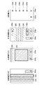
- the wiring provided in the horizontal direction corresponding to each row of the plurality of pixel circuits 220 is also referred to as an H scanning line.
- there are four H scanning lines 228 in one pixel circuit 220 (FIG. 5 shows the H scanning lines 228 by simulating the actual shape in the wiring layer. )
- the pixel circuit 220 is connected to a wiring (signal line) extending in the vertical direction for supplying a signal voltage corresponding to the video signal.
- a wiring signal line
- the wiring is provided for each column of the plurality of pixel circuits 220 arranged in a matrix.
- the wiring provided to extend in the vertical direction corresponding to each column of the plurality of pixel circuits 220 is also referred to as a V signal line.
- there is one V signal line 229 in one pixel circuit 220 in FIG. 5, the V signal line 229 is shown by simulating the actual shape in the wiring layer. )
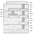
- FIG. 6 is a cross-sectional view schematically showing a stacked structure of the pixel circuit 220.
- FIG. 6 schematically shows a stacked structure from the diffusion layer to the anode of the organic light emitting diode 221 in the pixel circuit 220.
- the pixel circuit 220 includes a plurality of wiring layers 234, 237, and 240 formed on the diffusion layer 231.
- each of the transistors (transistors 222 to 226) is formed by forming an active region functioning as a source region, a drain region, and a channel region, a gate insulating film, a gate electrode, and the like on a semiconductor substrate such as Si. Is formed.
- illustration of elements formed in a diffusion layer such as a transistor is omitted.
- An insulator layer 232 (hereinafter referred to as a first insulator layer 232) is stacked on the diffusion layer 231.
- the first insulator layer 232 is formed by stacking insulators such as silicon oxide (SiO 2 ) with a predetermined thickness (a second insulator layer 235, a third insulator layer 238, and a second insulator layer described later). 4 insulator layer 241 is the same).
- the region and the upper layer are disposed at a position corresponding to a region connected to an upper wiring layer such as each electrode (source electrode, drain electrode, and gate electrode) of each transistor of the diffusion layer 231.
- a contact 233 for electrically connecting a wiring formed in a first wiring layer 234 described later is formed.
- the contact 233 is formed by forming a through hole (contact hole) in the first insulator layer 232 and then embedding a conductor such as tungsten (W) in the contact hole.
- a wiring layer 234 (hereinafter referred to as a first wiring layer 234) is formed on the first insulator layer 232 on which the contact 233 is formed.
- the first wiring layer 234 is formed by laminating a conductor such as aluminum (Al) with a predetermined thickness and then patterning the conductor film into a predetermined shape (a second wiring layer 237, which will be described later). The same applies to the third wiring layer 240).
- a conductor such as aluminum (Al)
- a second wiring layer 237 which will be described later.
- the third wiring layer 240 In the first wiring layer 234, the second wiring layer 237, and / or the third wiring layer 240, each wiring shown in FIG. 5 (various wiring including the H scanning line 228 and the V signal line 229) is formed.
- An insulator layer 235 (hereinafter referred to as a second insulator layer 235) is formed on the first wiring layer 234.
- the second insulator layer 235 is for electrically connecting a corresponding wiring formed in the lower first wiring layer 234 and a corresponding wiring formed in a second wiring layer 237 described later on the upper layer.
- a via 236 (hereinafter referred to as a first via 236) is formed.
- the first via 236 is formed by forming a through hole (via hole) in the second insulator layer 235 and then burying a conductor such as W in the via hole (second via 239 and third described later). The same applies to the via 242).
- a wiring layer 237 (hereinafter referred to as a second wiring layer 237) is formed on the second insulator layer 235 in which the first via 236 is formed.
- An insulator layer 238 (hereinafter referred to as a third insulator layer 238) is formed on the second wiring layer 237.
- the third insulator layer 238 is for electrically connecting a corresponding wiring formed in the lower second wiring layer 237 and a corresponding wiring formed in a third wiring layer 240 described later on the upper layer.
- a via 239 (hereinafter referred to as a second via 239) is formed.
- the wiring layer 240 (hereinafter referred to as the third wiring layer 240) is formed on the third insulator layer 238 in which the second via 239 is formed.
- An insulator layer 241 (hereinafter referred to as a fourth insulator layer 241) is formed on the third wiring layer 240.
- the fourth insulator layer 241 has vias 242 (hereinafter referred to as third vias 242) for electrically connecting corresponding wirings formed in the lower third wiring layer 240 and an anode 243 described later on the upper layer. ) Is formed.
- the pixel circuit 210 is manufactured by forming the organic light emitting diode 211 on the fourth insulator layer 241 in which the third via 242 is formed. Although only the anode 243 of the organic light emitting diode 211 is illustrated in FIG. 6, the organic light emitting diode 211 is formed by sequentially stacking an organic layer functioning as a light emitting layer and a cathode on the anode 243. .
- capacitive elements are formed in the second wiring layer 237 and the third wiring layer 240.
- the lower electrode (capacitor element lower electrode 251) of the capacitor element is formed on the second wiring layer 237.
- An upper electrode (capacitor element upper electrode 252) of the capacitor element is formed on the second wiring layer 237 via an insulator having a thickness corresponding to the capacitance of the capacitor element.
- the capacitive element upper electrode 252 is provided inside the third insulator layer 238. That is, although the description has been omitted above, the third insulator layer 238 is actually laminated in two stages with the capacitor element upper electrode 252 as a boundary.
- an insulator having a thickness corresponding to the capacitance of the capacitor element is laminated, and the capacitor element upper electrode 252 is formed thereon by the same method as that for the wiring layer. Thereafter, a third insulator layer 238 is formed by further laminating an insulator having a predetermined thickness.
- the second via 239 is also provided at a position corresponding to the capacitor element upper electrode 252.
- the capacitor element upper electrode 252 is electrically connected to the electrode 254 formed in the third wiring layer 240 by the second via 239.
- the electrode 254 is for extracting the potential of the capacitive element upper electrode 252 and is an electrode having the same potential as that of the capacitive element upper electrode 252. Therefore, the electrode 254 is also referred to as the capacitive element upper electrode 254 below. I will do it.
- each wiring that is, the H scanning line 228 and the V signal line 229 and the capacitor element (that is, the storage capacitor 227) included in the pixel circuit 210 will be examined.
- each of these wirings is formed in the first wiring layer 234, the second wiring layer 237, and / or the third wiring layer 240.
- the capacitive element lower electrode 251 and the capacitive element upper electrode 254 of the capacitive element are formed in the second wiring layer 237 and the third wiring layer 240, respectively.
- the capacitance element lower electrode 251 and the capacitance element upper electrode 254 of each wiring and the capacitance element can be formed in the same wiring layer.
- deterioration in luminance uniformity due to noise interference between electrodes due to increase in parasitic capacitance between wirings deterioration in luminance uniformity due to noise resistance deterioration due to pressure on the electrode area of the capacitive element
- pixel wiring is dense In other words, there are short circuit defects between wirings, wiring open defects due to skipping of a small area wiring pattern, and the like.
- the first wiring layer 234, the second wiring layer 237, and the third wiring are formed so as to prevent these problems as much as possible while keeping the pixel size small. It is important to devise the layout of the layer 240.
- the present inventors have come up with a suitable layout of the first wiring layer 234, the second wiring layer 237, and the third wiring layer 240 that can avoid the above-described problems.
- the preferred layout will be described in detail with reference to the drawings.
- FIG. 7 is a diagram for explaining an example of the layout of the wiring layer according to the present embodiment. 7 and FIGS. 8 to 10 described later schematically show the layout of the diffusion layer 231, the first wiring layer 234, the second wiring layer 237, and the third wiring layer 240. FIG.
- contacts and vias having “a” at the end of the reference numerals represent contacts and vias that are finally connected to the anode 243 in the upper layer. .
- contacts and vias having “b” at the end of the reference numerals represent contacts and vias that are finally connected to the capacitor lower electrode 251 in the upper layer.
- contacts and vias having “c” at the end of the reference sign represent contacts and vias that are finally connected to the V signal line 229 in the upper layer.
- contacts and vias with “d” at the end of the reference sign represent contacts and vias that are finally connected to the H scanning line 228 in the upper layer.
- the wiring related to the anode 243 (that is, the anode 243) is used for the first wiring layer 234, the second wiring layer 237, and the third wiring layer 240 for explanation.
- the wiring related to the capacitor element lower electrode 251 (that is, the capacitor element lower electrode 251 itself and the capacitor having the same potential as the capacitor element lower electrode 251) are thick solid lines and connected to the V signal line 229.
- the wiring (that is, the V signal line 229 itself and the wiring having the same potential as the V signal line 229) is a one-dot chain line, and the wiring related to the H scanning line 228 (that is, the same as the H scanning line 228 itself and the H scanning line 228).
- the potential wiring is shown by a thin solid line.
- FIG. 7 shows a layout example in the case where the H scanning line 228 and the V signal line 229 are formed in the first wiring layer 234 and the second wiring layer 237.
- the higher number of H scanning lines 228 and V signal lines 229 provided for one pixel circuit 220 is formed in the lower layer.
- the number of H scanning lines 228 provided for one pixel circuit 220 is larger than the number of V signal lines 229. Accordingly, as shown in the figure, if the H scanning line 228 and the V signal line 229 are formed in the first wiring layer 234 and the second wiring layer 237, the H scanning line 228 is formed in the first wiring layer 234. A V signal line 229 is formed in the second wiring layer 237.
- the first wiring layer 234 is connected to the H scanning line 228 and the corresponding electrode of the diffusion layer 231 to the anode 243 formed in the upper layer of the third wiring layer 240.
- Wiring (wiring indicated by a broken line in the drawing; hereinafter also referred to as connecting wiring related to the anode 243), wiring for connecting the corresponding electrode of the diffusion layer 231 to the capacitor element lower electrode 251 formed in the second wiring layer 237 (Wiring shown by a thick solid line in the figure.
- connection wiring relating to the capacitor also referred to as connection wiring relating to the capacitor
- connection wirings related to the V signal line 229 are also referred to as connection wirings related to the V signal line 229.
- connection wirings related to the capacitor element lower electrode 251 and the anode 243 are formed together with the V signal line 229.
- connection wirings related to the capacitor element upper electrode 254 and the anode 243 are formed in the third wiring layer 240. Note that one connection wiring related to the anode 243, one connection wiring related to the capacitor element, and one connection wiring related to the V signal line 229 are formed in each wiring layer.
- FIG. 8 shows a layout example of a wiring layer different from the present embodiment when the H scanning line 228 and the V signal line 229 are formed in the first wiring layer 234 and the second wiring layer 237.
- FIG. 8 is a diagram for comparison with the layout shown in FIG. 7.
- FIG. 6 is a diagram showing an example of a layout when an H scanning line 228 and a V signal line 229 are formed in different wiring layers. As shown in FIG. 8, contrary to the layout according to the present embodiment shown in FIG.
- the first wiring layer 234 includes the V signal line 229, the connection wiring related to the anode 243, the connection wiring related to the capacitor element, and the corresponding electrode of the diffusion layer 231.
- Wiring for connecting to the H scanning line 228 formed in the layer 237 (wiring shown by a thin solid line in the drawing; hereinafter also referred to as connection wiring relating to the H scanning line 228) is formed.
- the number of connection wirings related to the H scanning line 228 is formed according to the number of the H scanning lines 228.
- connection wirings related to the capacitor element lower electrode 251 and the anode 243 are formed together with the H scanning lines 228 in which a larger number exists.
- connection wirings related to the capacitor element upper electrode 254 and the anode 243 are formed in the third wiring layer 240.
- the H scanning line 228 that is a larger number of wirings is the lower first wiring layer 234. Therefore, the wiring pattern of the first wiring layer 234 is relatively dense.
- the H scanning lines 228, which are more wirings are not formed in the first wiring layer 234, but the number of connection wirings related to the H scanning lines 228 corresponds to the number of H scanning lines 228. Only the first wiring layer 234 needs to be formed. Therefore, although the connection wiring related to the H scanning line 228 has a smaller area than the H scanning line 228, as a result, the density of the wiring pattern in the first wiring layer 234 is different from the layout according to the present embodiment. It is not much smaller than that.
- the V signal line 229 which is a smaller number of wires, is formed in the second wiring layer 237, so that the wiring pattern of the second wiring layer 237 is relatively sparse. Become.
- the wiring pattern of the second wiring layer 237 is relatively dense.
- the H scanning lines 228 and the V signal lines 229 are provided on the lower layer of the H scanning lines 228 which are the wirings having a larger number provided for one pixel circuit 220.
- the layout of the first wiring layer 234 and the second wiring layer 237 so as to be formed in the one wiring layer 234, it becomes possible to make the wiring pattern in the second wiring layer 237 in a higher layer more sparse. .
- the sparser wiring pattern in the second wiring layer 237 Due to the sparser wiring pattern in the second wiring layer 237, the above-described deterioration in luminance uniformity due to the increase in the parasitic capacitance between the wirings in the second wiring layer 237, the occurrence of a short circuit failure between the wirings, and the like. It becomes possible to suppress.
- the capacitor element lower electrode 251 since the capacitor element lower electrode 251 is provided in the second wiring layer 237, the wiring pattern of the second wiring layer 237 becomes sparse, so that the flexibility of the layout of the capacitor element lower electrode 251 is increased. In addition, it is possible to secure a sufficient area for realizing the desired capacitance for the capacitor element lower electrode 251.
- FIG. 7 shows one layout example in the case where the H scanning line 228 and the V signal line 229 are formed in the first wiring layer 234 and the second wiring layer 237, respectively, but this embodiment is limited to such an example.
- the layout method according to the present embodiment (that is, a method of forming a higher number of H scanning lines 228 and V signal lines 229 for one pixel circuit 220 in a lower layer) is the H scanning line 228.
- the present invention is applicable even when the V signal line 229 is formed in another wiring layer.
- FIG. 9 is a diagram for explaining another example of the layout of the wiring layer according to the present embodiment.
- FIG. 9 shows a layout example when the H scanning line 228 and the V signal line 229 are formed in the first wiring layer 234, the second wiring layer 237, and the third wiring layer 240.
- the higher number of H scanning lines 228 and V signal lines 229 provided for one pixel circuit 220 is formed in a lower layer.
- the H scanning line 228 is formed in the first wiring layer 234 and the second wiring layer 237
- the V signal line 229 is formed in the third wiring layer 240.
- the first wiring layer 234 includes a part of the H scanning lines 228 (three in the illustrated example), a connection wiring related to the anode 243, and a connection wiring related to the capacitive element. , And a connection wiring relating to the V signal line 229 is formed.
- the remaining H scanning lines 228 are formed, as well as the capacitor element lower electrode 251, the connection wiring for the anode 243, and the connection wiring for the V signal line 229. Is done.
- connection wirings related to the capacitor element upper electrode 254 and the anode 243 are formed together with the V signal line 229.
- the plurality of H scanning lines 228 are formed in the same wiring layer. However, in this embodiment, the plurality of H scanning lines 228 are distributed and formed in different wiring layers. May be.
- FIG. 10 is different from the present embodiment in the case where the H scanning line 228 and the V signal line 229 are formed in the first wiring layer 234, the second wiring layer 237, and the third wiring layer 240.
- An example of a layout of a wiring layer is shown.
- FIG. 10 is a diagram for comparison with the layout shown in FIG. 9, in which the H scanning line 228 and the V signal line 229 are formed in the first wiring layer 234, the second wiring layer 237, and the third wiring layer 240.
- FIG. 4 is a diagram showing a layout example when the H scanning line 228 and the V signal line 229 are formed in a wiring layer different from the present embodiment. As shown in FIG. 10, contrary to the layout according to the present embodiment shown in FIG.
- the larger number of H scanning lines 228 and V signal lines 229 provided for one pixel circuit 220 is It is assumed that the upper layer is formed.
- the V signal line 229 is formed in the first wiring layer 234 and the H scanning line 228 is formed in the third wiring layer 240.
- the first wiring layer 234 is formed with the V signal line 229, the connection wiring related to the anode 243, the connection wiring related to the capacitive element, and the connection wiring related to the H scanning line 228.
- the in the second wiring layer 237 the connection wiring related to the anode 243 and the connection wiring related to the H scanning line 228 are formed together with the capacitor element lower electrode 251.
- the number of connection wirings related to the H scanning line 228 is formed according to the number of the H scanning lines 228.
- connection wirings related to the capacitor element upper electrode 254 and the anode 243 are formed together with the H scanning lines 228 in which a larger number exists.
- the layout according to the present embodiment Comparing the layout according to the present embodiment shown in FIG. 9 with the layout shown in FIG. 10, in the layout according to the present embodiment, most of the H scanning lines 228 which are more wirings are lower first wirings. Since it is formed in the layer 234, the wiring pattern of the first wiring layer 234 is relatively dense. On the other hand, in the layout shown in FIG. 8, the H scanning lines 228, which are more wirings, are not formed in the first wiring layer 234, but the number of connection wirings related to the H scanning lines 228 corresponds to the number of H scanning lines 228. Only the first wiring layer 234 needs to be formed. Therefore, although the connection wiring related to the H scanning line 228 has a smaller area than the H scanning line 228, as a result, the density of the wiring pattern in the first wiring layer 234 is different from the layout according to the present embodiment. It is not much smaller than that.
- the V signal line 229 which is a smaller number of wirings, is formed in the third wiring layer 240. Therefore, the wiring patterns of the second wiring layer 237 and the third wiring layer 240 are used. Is relatively sparse.
- the H scanning line 228, which is the wiring having a larger number of the H scanning lines 228 and the V signal lines 229 provided for one pixel circuit 220, is provided at a lower layer.
- the layout of the first wiring layer 234, the second wiring layer 237, and the third wiring layer 240 so as to be formed in the first wiring layer 234 and the second wiring layer 237, the second wiring layer of the upper layer is formed.
- the wiring patterns in 237 and the third wiring layer 240 can be made sparser. Therefore, it is possible to obtain the same effect as when the layout shown in FIG. 7 described above is applied, that is, it is possible to realize the display device 1 with higher definition and higher reliability.
- a large number of wirings are formed by the lower wiring layer, so that a large number of wirings are formed by the upper wiring layer, and the connection wiring (the above-described H scanning line described above) is isolated from the lower wiring layer.
- the wiring pattern of the lower wiring layer is not less dense.
- the wiring pattern in the lower wiring layer closer to the diffusion layer 231 in which each transistor is formed becomes dense, the light shielding effect on the transistor can be improved. Therefore, the characteristic variation of the transistor due to light exposure can be further suppressed, and the reliability of the display device 1 can be further improved.
- the wiring pattern in the upper wiring layer, particularly the uppermost wiring layer can be made relatively sparse, the anode 243 of the organic light emitting diode 221 formed further above the uppermost wiring layer.
- the flatness of the film can be improved. Thereby, the luminous efficiency of the organic light emitting diode 221 can be improved, and the display quality can be further improved.
- connection wirings related to the anode 243 formed on the third wiring layer 240 which is the uppermost wiring layer that is, The degree of freedom of the arrangement of the third via 242 connecting the connection wiring related to the anode 243 and the upper layer anode 243 is improved. This makes it easier to design the pixel layout.
- FIG. 11 is a diagram illustrating an example of the arrangement of the third vias 242 in the three subpixels when one pixel is formed by the three subpixels.
- FIG. 12 is a diagram illustrating an example of the arrangement of the third vias 242 in the four subpixels when one pixel is formed by the four subpixels.
- FIG. 11 and 12 both are top views of a configuration in which an anode 243 and an organic layer 261 (a layer functioning as a light emitting layer in the organic light emitting diode 221) corresponding to one pixel are stacked on the left side in the drawing.
- the arrangement of the third via 242 for such a configuration is schematically shown.
- the arrangement of the third via 242 for such a configuration is schematically shown.
- the configuration 262 in which the diffusion layer 231 and the wiring layer are stacked is not illustrated in detail inside each layer for the sake of simplicity.
- the structure 262 in which the organic layer 261, the diffusion layer 231 and the wiring layer are stacked has characters (R: Red, G: Green, B: representing the color of the corresponding sub-pixel). Blue, W: White) is added to the end of the code.
- RGB Red, G: Green, B: representing the color of the corresponding sub-pixel
- Blue, W White
- CF color filter
- the arrangement of the third vias 242 is substantially the same in each subpixel. Therefore, there is not much merit by improving the degree of freedom of arrangement of the third via 242.
- the arrangement of the third vias 242 is different in each subpixel. That is, it is necessary to change the arrangement of the connection wiring related to the anode 243 in the third wiring layer 240 for each subpixel.
- the layout as shown in FIG. 10 is performed, if the wiring pattern in the third wiring layer 240 is dense, the degree of freedom of arrangement of the connection wiring related to the anode 243 is low. Therefore, in order to make the arrangement of the connection wiring related to the anode 243 different for each subpixel, there is a possibility that the entire layout of the third wiring layer 240 needs to be different for each subpixel. In this case, the layout of the lower second wiring layer 237 and the first wiring layer 234 may need to be different for each sub-pixel accordingly, so that the amount of work for layout becomes enormous and a heavy burden on the designer. Become.
- the wiring pattern of the upper wiring layer can be made relatively sparse, so that the degree of freedom of the arrangement of the connection wiring related to the anode 243 in the third wiring layer 240 is increased. high. Therefore, the layout of the third wiring layer 240 can be configured so that only the arrangement of the connection wirings related to the anode 243 is different for each subpixel, and the other wirings are the same for each subpixel. In this case, regarding the layout of the lower second wiring layer 237 and the first wiring layer 234, only the arrangement of the connection wiring related to the anode 243 needs to be different for each sub-pixel, so that the difficulty in designing the layout is lowered.
- the third via 242 (that is, the uppermost wiring layer and the uppermost wiring layer) is formed for each subpixel as in the case where one pixel is formed by four subpixels.
- the arrangement of vias connecting to the anode 243 is different, there is also an effect that the difficulty of layout design of the pixel can be reduced.
- the wiring layer layout according to the present embodiment has been described above. In the above, only the two layout examples shown in FIGS. 7 and 9 are taken up. However, when the number of wiring layers is different from the three layers exemplified above (for example, when there are more than four layers), When the arrangement positions of the H scanning lines 228 and the V signal lines 229 in the wiring layer are different, when the numbers of the H scanning lines 228 and the V signal lines 229 are different (for example, when there are a plurality of both), one pixel circuit 210, Even when the magnitude relationship between the numbers of the H scanning lines 228 and the V signal lines 229 provided for 220 is opposite, the wiring layer layout method according to the present embodiment can be applied.
- the wiring layer layout method according to the present embodiment can be applied to various display devices as long as the display device is driven by an active matrix method. Regardless of the number of wiring layers and the like, the number of connection wirings related to the H scanning line 228 or V signal line 229 in the lower wiring layer is applied by applying the wiring layer layout method according to the present embodiment. As a result, the wiring pattern of the upper wiring layer can be made relatively sparse. Further, by providing a capacitor element electrode (capacitor element lower electrode 251 and / or capacitor element upper electrode 254) in a wiring layer having a relatively sparse wiring pattern, a sufficient area of the capacitor element electrode is ensured. be able to. Accordingly, as in the above-described embodiment, various effects such as improved reliability can be obtained.
- FIG. 13 is a cross-sectional view illustrating a specific configuration example of the display device 1 according to the present embodiment.
- FIG. 13 shows a partial cross-sectional view of the display device 1.
- the display device 1 is provided on a first substrate 11 with a plurality of organic light emitting diodes 211 that are light emitting elements that emit white light, and an upper layer of the organic light emitting diodes 211.
- a second substrate 34 formed of a material transparent to the light from the organic light emitting diode 211 is disposed on the CF layer 33.
- the first substrate 11 is provided with a thin film transistor (TFT) 15 for driving the organic light emitting diode 211 corresponding to each of the organic light emitting diodes 211.
- TFT thin film transistor
- the TFT 15 corresponds to each transistor (the driving transistor 212, the sampling transistor 213, the light emission control transistor 214, and the switching transistor 217) that constitutes the pixel circuit 210 described above.
- An arbitrary organic light emitting diode 211 is selectively driven by the TFT 15, and the light from the driven organic light emitting diode 211 passes through the corresponding CF so that the color is appropriately converted, and from above through the second substrate 34.
- a desired image, a character, etc. are displayed by being emitted.
- the stacking direction of the layers in the display device 1 is also referred to as the vertical direction.
- the direction in which the first substrate 11 is disposed is defined as a downward direction
- the direction in which the second substrate 34 is disposed is defined as an upward direction.
- a surface perpendicular to the vertical direction is also referred to as a horizontal plane.
- the display device 1 shown in FIG. 13 is a top emission type display device that can be displayed in color and is driven by an active matrix method.
- this embodiment is not limited to such an example, and the display device 1 according to this embodiment may be a bottom emission type display device that emits light through the first substrate 11.
- the first substrate 11 is composed of a Si substrate.
- the second substrate 34 is made of quartz glass.
- this embodiment is not limited to this example, and various known materials may be used for the first substrate 11 and the second substrate 34.
- the first substrate 11 and the second substrate 34 are a high strain point glass substrate, a soda glass (mixture of Na 2 O, CaO and SiO 2 ) substrate, a borosilicate glass (Na 2 O, B 2 O 3 and SiO 2).
- substrate 34 may be the same, and may differ. However, since the display device 1 is a top emission type as described above, the second substrate 34 is preferably formed of a material having a high transmittance that can suitably transmit the light from the organic light emitting diode 211.
- the organic light emitting diode 211 includes a first electrode 21, an organic layer 23 provided on the first electrode 21, and a second electrode 22 formed on the organic layer 23. More specifically, a second member 52 provided with an opening 25 so as to expose at least a part of the first electrode 21 is laminated on the first electrode 21, and the organic layer 23 is It is provided on the first electrode 21 exposed at the bottom of the opening 25. That is, the organic light emitting diode 211 has a configuration in which the first electrode 21, the organic layer 23, and the second electrode 22 are stacked in this order in the opening 25 of the second member 52. This stacked structure functions as the light emitting portion 24 of each pixel. That is, the portion of the organic light emitting diode 211 that contacts the opening 25 of the second member 52 is the light emitting surface.
- the second member 52 functions as a pixel definition film that is provided between the pixels and defines the area of the pixels.
- the organic layer 23 includes a light emitting layer made of an organic light emitting material and is configured to emit white light.
- the specific configuration of the organic layer 23 is not limited, and may be various known configurations.
- the organic layer 23 has a stacked structure of a hole transport layer, a light emitting layer, and an electron transport layer, a stacked structure of a hole transport layer and a light emitting layer that also serves as an electron transport layer, or a hole injection layer and a hole transport. It can be composed of a laminated structure of a layer, a light emitting layer, an electron transport layer, and an electron injection layer.
- the organic layer 23 may have a two-stage tandem structure in which a first tandem unit, a connection layer, and a second tandem unit are laminated. Good.
- the organic layer 23 may have a three or more tandem structure in which three or more tandem units are stacked.
- the organic layer 23 that emits white as a whole can be obtained by changing the luminescent color of the light emitting layer between red, green, and blue in each tandem unit.
- the organic layer 23 is formed by vacuum-depositing an organic material.
- the organic layer 23 may be formed by various known methods.
- the organic layer 23 may be formed by a physical vapor deposition method (PVD method) such as a vacuum deposition method, a printing method such as a screen printing method or an ink jet printing method, a laser absorption layer formed on a transfer substrate, and the like.
- PVD method physical vapor deposition method
- a laser transfer method in which the organic layer on the laser absorption layer is separated by irradiating a laser on the stacked structure of the organic layer and the organic layer is transferred, or various coating methods can be used.
- the first electrode 21 functions as an anode. That is, the first electrode 21 corresponds to the anode 243 shown in FIG. Since the display device 1 is a top emission type as described above, the first electrode 21 is formed of a material that can reflect light from the organic layer 23. In the illustrated configuration example, the first electrode 21 is formed of an alloy of aluminum and neodymium (Al—Nd alloy). The film thickness of the first electrode 21 is, for example, about 0.1 ⁇ m to 1 ⁇ m. However, the present embodiment is not limited to such an example, and the first electrode 21 is formed of various known materials used as a material for a light reflection side electrode that functions as an anode in a general organic EL display device. can do. Further, the film thickness of the first electrode 21 is not limited to the above example, and the first electrode 21 can be appropriately formed within a film thickness range generally employed in an organic EL display device.
- the first electrode 21 includes platinum (Pt), gold (Au), silver (Ag), chromium (Cr), tungsten (W), nickel (Ni), copper (Cu), iron (Fe), cobalt ( Co) or a metal having a high work function such as tantalum (Ta), or an alloy (for example, 0.3% by mass to 1% by mass of palladium (Pd) and 0.3% by mass to 1% by mass of silver as a main component)
- a metal having a high work function such as tantalum (Ta), or an alloy (for example, 0.3% by mass to 1% by mass of palladium (Pd) and 0.3% by mass to 1% by mass of silver as a main component)
- an Ag—Pd—Cu alloy containing 1% copper or an Al—Nd alloy for example, an Ag—Pd—Cu alloy containing 1% copper or an Al—Nd alloy.
- a conductive material having a small work function value and high light reflectance such as aluminum or an alloy containing aluminum can be used
- the first electrode 21 has a hole injection property such as an oxide of indium and tin (ITO) or an oxide of indium and zinc (IZO) on a highly reflective film such as a dielectric multilayer film or aluminum. It is also possible to have a structure in which transparent conductive materials excellent in thickness are laminated.
- ITO indium and tin
- IZO oxide of indium and zinc
- the second electrode 22 functions as a cathode.
- the second electrode 22 is formed of a material that can transmit light from the organic layer 23.
- the second electrode 22 is formed of an alloy of magnesium and silver (Mg—Ag alloy).
- the film thickness of the second electrode 22 is, for example, about 10 nm.
- the present embodiment is not limited to this example, and the second electrode 22 is formed of various known materials that are used as a material of an electrode on the light transmission side that functions as a cathode in a general organic EL display device. can do.
- the film thickness of the second electrode 22 is not limited to the above example, and the second electrode 22 can be appropriately formed within a film thickness range generally employed in an organic EL display device.
- the second electrode 22 is made of aluminum, silver, magnesium, calcium (Ca), sodium (Na), strontium (Sr), an alloy of alkali metal and silver, or an alloy of alkaline earth metal and silver (for example, magnesium). And an alloy of Mg and Ag (Mg—Ag alloy), an alloy of magnesium and calcium (Mg—Ca alloy), an alloy of aluminum and lithium (Al—Li alloy), and the like.
- the thickness of the second electrode 22 is, for example, about 4 nm to 50 nm.
- the second electrode 22 may have a structure in which the material layer described above and a transparent electrode made of, for example, ITO or IZO (for example, a thickness of about 30 nm to 1 ⁇ m) are stacked from the organic layer 23 side.
- a transparent electrode made of, for example, ITO or IZO (for example, a thickness of about 30 nm to 1 ⁇ m)
- the thickness of the material layer described above can be reduced to, for example, about 1 nm to 4 nm.
- the 2nd electrode 22 may be comprised only with a transparent electrode.
- a bus electrode (auxiliary electrode) made of a low resistance material such as aluminum, aluminum alloy, silver, silver alloy, copper, copper alloy, gold, or gold alloy is provided for the second electrode 22, and the second electrode 22 as a whole. The resistance may be reduced.
- the first electrode 21 and the second electrode 22 are formed by depositing a material by a predetermined thickness by a vacuum evaporation method and then patterning the film by an etching method.
- this embodiment is not limited to this example, and the first electrode 21 and the second electrode 22 may be formed by various known methods.
- the method for forming the first electrode 21 and the second electrode 22 include an electron beam vapor deposition method, a hot filament vapor deposition method, a vapor deposition method including a vacuum vapor deposition method, a sputtering method, a chemical vapor deposition method (CVD method), and an organic method.
- MOCVD Metal chemical vapor deposition
- various printing methods for example, screen printing, ink jet printing, or metal mask printing
- plating (electroplating) Method for example, electroless plating method, etc.
- lift-off method for example, laser ablation method, sol-gel method and the like.
- the second member 52 is formed by depositing SiO 2 to a predetermined thickness by a CVD method and then patterning the SiO 2 film using a photolithography technique and an etching technique.
- the material of the second member 52 is not limited to this example, and various materials having insulating properties can be used as the material of the second member 52.
- examples of the material constituting the second member 52 include SiO 2 , MgF, LiF, polyimide resin, acrylic resin, fluororesin, silicone resin, fluoropolymer, and silicone polymer.
- the second member 52 is formed of a material having a refractive index lower than that of the material of the first member 51.
- the first electrode 21 constituting the organic light emitting diode 211 is provided on the interlayer insulating layer 16 made of SiON.
- the interlayer insulating layer 16 covers the light emitting element driving unit formed on the first substrate 11.
- the light emitting element driving unit is composed of a plurality of TFTs 15. That is, the light emitting element driving unit corresponds to the driving circuit of the pixel circuit 210.
- the TFT 15 includes a gate electrode 12 formed on the first substrate 11, a gate insulating film 13 formed on the first substrate 11 and the gate electrode 12, and a semiconductor layer 14 formed on the gate insulating film 13.
- the TFT 15 is a bottom gate type, but the present embodiment is not limited to this example, and the TFT 15 may be a top gate type.
- An interlayer insulating layer 16 (a lower interlayer insulating layer 16A and an upper interlayer insulating layer 16B) having two layers is laminated on the upper layer of the semiconductor layer 14 by a CVD method.
- the source / drain region 14B is exposed to a portion corresponding to the source / drain region 14B of the lower interlayer insulating layer 16A using, for example, a photolithography technique and an etching technique.
- a contact hole 17 is provided in the substrate, and a wiring 18 made of aluminum is formed so as to fill the contact hole 17.
- the wiring 18 is formed by combining, for example, a vacuum deposition method and an etching method.
- the upper interlayer insulating layer 16B is laminated.
- a contact hole 19 is provided in a portion of the upper interlayer insulating layer 16B where the wiring 18 is provided so as to expose the wiring 18 by using, for example, a photolithography technique and an etching technique.
- the first electrode 21 of the organic light emitting diode 211 is formed, the first electrode 21 is formed so as to be in contact with the wiring 18 through the contact hole 19.
- the organic light emitting diode 211 has a first electrode 21 corresponding to the source / drain region 14B of the TFT 15 via the wiring 18 (in the pixel circuit example shown in FIG. ) And electrically connected.
- the interlayer insulating layer 16 is made of SiON, but the present embodiment is not limited to this example.
- the interlayer insulating layer 16 may be formed of various known materials that can be used as an interlayer insulating layer in a general organic EL display device.
- a SiO 2 material for example, SiO 2 , BPSG, PSG, BSG, AsSG, PbSG, SiON, SOG (spin on glass), low melting glass, glass paste, etc.
- SiN materials and insulating resins for example, polyimide resins, novolac resins, acrylic resins, polybenzoxazoles, etc.
- insulating resins for example, polyimide resins, novolac resins, acrylic resins, polybenzoxazoles, etc.
- the method for forming the interlayer insulating layer 16 is not limited to the above example, and the interlayer insulating layer 16 can be formed by a known method such as a CVD method, a coating method, a sputtering method, or various printing methods. .
- the wiring 18 is formed by forming and patterning aluminum by vacuum deposition and etching, but this embodiment is not limited to this example.
- the wiring 18 may be formed by forming and patterning various materials used as wiring in a general organic EL display device by various methods.
- FIG. 13 only one wiring layer is shown for simplicity. Actually, as described with reference to FIG. 6, a plurality of wiring layers may be formed on the diffusion layer on which the TFT 15 is formed, and the organic light emitting diode 211 may be further formed thereon.
- the opening 25 provided in the second member 52 of the organic light emitting diode 211 is formed such that its sidewall has a tapered shape that is inclined so that the opening area increases as it goes downward.
- the first member 51 is embedded in the opening 25. That is, the first member 51 is a layer that is provided immediately above the light emitting surface of the organic light emitting diode 211 and propagates light emitted from the light emitting element upward.
- the first member 51 has a substantially trapezoidal cross-sectional shape in the stacking direction (that is, the cross-sectional shape shown in the drawing), and a bottom surface on the upper side. Has a truncated pyramid shape.
- the first member 51 is formed by depositing Si 1-x N x by vacuum deposition so as to fill the opening 25, and then the surface of the Si 1-x N x film is formed by chemical mechanical polishing (CMP method) or the like. It is formed by flattening.
- the material of the first member 51 is not limited to this example, and as the material of the first member 51, various materials having insulating properties can be used.
- the material constituting the first member 51 includes Si 1-x N x , ITO, IZO, TiO 2 , Nb 2 O 5 , bromine-containing polymer, sulfur-containing polymer, titanium-containing polymer, or zirconium-containing polymer. Can be mentioned.
- the method for forming the first member 51 is not limited to this example, and various known methods may be used as the method for forming the first member 51.
- the refractive index n 1 of the first member 51 so that the refractive index n 2 of the second member 52 satisfies the relationship of n 1> n 2
- the first member 51 and second member 52 Materials are selected.
- the first member 51 is provided immediately above the light emitting surface of the organic light emitting diode 211 as described above. Since the first member 51 has a truncated pyramid shape with the bottom surface facing upward, the light emitted from the light emitting surface of the organic light emitting diode 211 is the interface between the first member 51 and the second member 52, that is, The light is reflected upward by the reflector 53, which is the light emission direction.
- the reflector 53 by providing the reflector 53, the extraction efficiency of the emitted light from the organic light emitting diode 211 can be improved, and the luminance of the display device 1 as a whole can be improved.
- the refractive indexes of the first member 51 and the second member 52 are n 1 ⁇ n. It is preferable to satisfy the relationship of 2 ⁇ 0.20. More preferably, it is desirable that the refractive indexes of the first member 51 and the second member 52 satisfy a relationship of n 1 ⁇ n 2 ⁇ 0.30.
- the shape of the first member 51 is such that 0.5 ⁇ R 1 / R 2 ⁇ 0.8 and 0.5 ⁇ H / It is preferable to satisfy the relationship of R 1 ⁇ 0.8.
- R 1 is the diameter of the light incident surface of the first member 51 (that is, the portion facing downward in the stacking direction and facing the light emitting surface of the organic light emitting diode 211), and R 2 is the first member.
- H is the distance (height in the stacking direction) between the bottom surface and the top surface when the first member 51 is regarded as a truncated cone. is there.
- a protective film 31 and a planarizing film 32 are stacked in this order on the planarized first member 51.
- the protective film 31 is formed, for example, by stacking Si 1-y N y by a predetermined film thickness (about 3.0 ⁇ m) by vacuum deposition.
- the planarizing film 32 is formed, for example, by laminating SiO 2 by a predetermined film thickness (about 2.0 ⁇ m) by a CVD method and planarizing the surface by a CMP method or the like.
- the material and film thickness of the protective film 31 and the planarizing film 32 are not limited to this example, and the protective film 31 and the planarizing film 32 are used as a protective film and a planarizing film for a general organic EL display device. Depending on the various known materials, it may be appropriately formed so as to have a film thickness generally employed in organic EL display devices.
- the protective film 31 has a refractive index n 3 that is equal to or smaller than the refractive index n 1 of the first member 51 or the refractive index n 1 of the first member 51. 31 materials are selected. Further, preferably, the refractive index n 3 of the protective film 31, the absolute value of the difference between the refractive index n 4 of the planarization film 32 is 0.30 or less, more preferably to be 0.20 or less, the protective film 31 and the material of the planarizing film 32 are selected.
- the light emitted from the organic light emitting diode 211 is transmitted to the interface between the first member 51 and the protective film 31, and the protective film 31 and the planarizing film 32. Can be suppressed from being reflected or scattered at the interface with the light, and the light extraction efficiency can be further improved.
- the display device 1 is a so-called on-chip color filter (OCCF) type display device in which the CF layer 33 is formed on the first substrate 11 on which the organic light emitting diode 211 is formed.
- the display device 1 is manufactured by attaching the second substrate 34 to the upper layer of the CF layer 33 via a sealing resin film 35 such as an epoxy resin.
- a sealing resin film 35 such as an epoxy resin.
- the material of the sealing resin film 35 is not limited to this example, and the material of the sealing resin film 35 is highly transmissive to the light emitted from the organic light emitting diode 211, and the CF layer 33 and the upper layer located in the lower layer.
- the display device 1 includes the first substrate 11 such that the CF layer 33 is formed on the second substrate 34 and the CF layer 33 faces the organic light emitting diode 211. It may be a so-called counter-CF display device manufactured by bonding the second substrate 34 and the second substrate 34 together.
- the CF layer 33 is formed so that each color CF having a predetermined area is provided for each of the organic light emitting diodes 211.
- the CF layer 33 can be formed, for example, by exposing and developing a resist material in a predetermined shape using a photolithography technique.
- the film thickness of the CF layer 33 is, for example, about 2 ⁇ m.
- the material, the forming method, and the film thickness of the CF layer 33 are not limited to such examples, and the CF layer 33 may be any of various known materials used as a CF layer in a general organic EL display device, and various types of materials. It may be appropriately formed by a known method so as to have a film thickness generally employed in an organic EL display device.
- the CF layer 33 is configured such that red CF33R, green CF33G, and blue CF33B each having a predetermined area are continuously distributed in a horizontal plane.
- red CF33R, green CF33G, and blue CF33B each having a predetermined area are continuously distributed in a horizontal plane.
- CF33a when it is not necessary to distinguish between CF33R, CF33G, and CF33B, one or more of them are simply referred to as CF33a.
- One sub-pixel is formed by a combination of one organic light emitting diode 211 and one CF 33a.
- the specific configuration example of the display device 1 has been described above.
- the configuration of the display device 1 described above particularly the configuration of the reflector 53, reference can be made to, for example, Japanese Patent Application Laid-Open No. 2013-191533, which is a prior application by the present applicant.
- the configuration of the display device 1 according to the present embodiment is not limited to such an example.
- the display device 1 according to the present embodiment only needs to reflect the points described in (4. Layout of wiring layers), and other points are used in a general display device.
- Various known configurations can be applied.
- FIG. 14 is a diagram illustrating an appearance of a smartphone, which is an example of an electronic device to which the display device 1 according to this embodiment can be applied.
- the smartphone 501 includes an operation unit 503 that includes buttons and receives an operation input by a user, and a display unit 505 that displays various types of information.
- the display device 1 can be applied to the display unit 505.
- FIGS. 15 and 16 are views showing the appearance of a digital camera, which is another example of an electronic apparatus to which the display device 1 according to this embodiment can be applied.
- FIG. 15 shows an appearance of the digital camera 511 viewed from the front (subject side)
- FIG. 16 shows an appearance of the digital camera 511 viewed from the rear.
- the digital camera 511 displays a main body (camera body) 513, an interchangeable lens unit 515, a grip 517 held by a user at the time of shooting, and various types of information.
- a monitor 519 and an electronic view finder (EVF) 521 that displays a through image observed by the user at the time of shooting.
- the display device 1 can be applied to the monitor 519 and the EVF 521.
- FIG. 17 is a diagram illustrating an appearance of a head mounted display (HMD), which is another example of an electronic apparatus to which the display device 1 according to the present embodiment can be applied.
- the HMD 531 includes a glasses-shaped display unit 533 that displays various types of information, and an ear hooking unit 535 that is hooked on the user's ear when worn.
- the display device 1 can be applied to the display unit 533.
- the electronic apparatus to which the display device 1 can be applied is not limited to those exemplified above, and the display device 1 may be, for example, a television device, an electronic book, a smartphone, a portable information terminal (PDA: Personal Digital Assistant), a notebook, or the like. Applicable to display devices mounted on electronic devices in all fields that display based on externally input image signals or internally generated image signals such as type PCs (Personal Computers), video cameras, or game machines Is possible.
- type PCs Personal Computers
- video cameras or game machines
- each transistor (the driving transistor 212, the sampling transistor 213, the light emission control transistor 214, and the switching transistor 217) included in the driving circuit of the pixel circuit 210 is a P-channel type.
- Such a technique is not limited to such an example.
- these transistors may be N-channel type.
- a pixel unit configured by arranging a plurality of pixel circuits each including a light emitting element and a driving circuit for driving the light emitting element in a matrix; and A wiring connected to each of the pixel circuits, the scanning line provided extending in a first direction corresponding to each row of the plurality of pixel circuits; A wiring connected to each of the pixel circuits, the signal line extending in a second direction orthogonal to the first direction corresponding to each column of the plurality of pixel circuits;
- the larger number provided for one pixel circuit is located in a lower wiring layer
- the electrode of the capacitive element included in the drive circuit is located in a wiring layer provided with either the scanning line or the signal line.
- the drive circuit has a plurality of transistors, A plurality of wiring layers in which the scanning lines, the signal lines, and the capacitor elements are formed are stacked on a diffusion layer in which a plurality of the transistors are formed.
- the light emitting element is an organic light emitting diode;
- the organic light emitting diode is located on the uppermost wiring layer;
- One subpixel is constituted by one pixel circuit, One pixel is constituted by the four sub-pixels.
- the number of scanning lines is greater than the number of signal lines, The display device according to any one of (1) to (4).
- the scanning line is a wiring extending in a horizontal direction
- the signal line is a wiring extending in the vertical direction.
- the display device according to any one of (1) to (5).
- All of the plurality of scanning lines are located in the same wiring layer, or all of the plurality of signal lines are located in the same wiring layer, The display device according to any one of (1) to (6).
- a plurality of the scanning lines are arranged in a plurality of different wiring layers, or a plurality of the signal lines are arranged in a plurality of different wiring layers.
- a display device for performing display based on a video signal With The display device A pixel unit configured by arranging a plurality of pixel circuits each including a light emitting element and a driving circuit for driving the light emitting element in a matrix; and A wiring connected to each of the pixel circuits, the scanning line provided extending in a first direction corresponding to each row of the plurality of pixel circuits; A wiring connected to each of the pixel circuits, the signal line extending in a second direction orthogonal to the first direction corresponding to each column of the plurality of pixel circuits; Have Of the scanning lines and the signal lines, the larger number provided for one pixel circuit is located in a lower wiring layer, The electrode of the capacitive element included in the drive circuit is located in a wiring layer provided with either the scanning line or the signal line. Electronics.
Landscapes
- Engineering & Computer Science (AREA)
- Microelectronics & Electronic Packaging (AREA)
- Physics & Mathematics (AREA)
- Geometry (AREA)
- Power Engineering (AREA)
- General Physics & Mathematics (AREA)
- Computer Hardware Design (AREA)
- Condensed Matter Physics & Semiconductors (AREA)
- Theoretical Computer Science (AREA)
- Optics & Photonics (AREA)
- Electroluminescent Light Sources (AREA)
- Control Of El Displays (AREA)
- Control Of Indicators Other Than Cathode Ray Tubes (AREA)
- Devices For Indicating Variable Information By Combining Individual Elements (AREA)
Abstract
【課題】より信頼性を向上させることが可能になる。 【解決手段】発光素子及び当該発光素子を駆動するための駆動回路から構成される画素回路が行列状に複数並べられて構成される画素部と、前記画素回路の各々に接続される配線であって、複数の前記画素回路の各行に対応して第1の方向に延伸して設けられる走査線と、前記画素回路の各々に接続される配線であって、複数の前記画素回路の各列に対応して前記第1の方向と直交する第2の方向に延伸して設けられる信号線と、を備え、前記走査線及び前記信号線のうちで、1つの前記画素回路に対して設けられる本数がより多い方が、より下層の配線層に位置し、前記駆動回路に含まれる容量素子の電極が、前記走査線及び前記信号線のいずれかが設けられる配線層に位置する、表示装置を提供する。
Description
本開示は、表示装置及び電子機器に関する。
いわゆるアクティブマトリックス方式によって駆動される表示装置では、表示面の横方向(以下、水平方向ともいう)に沿って延伸し、表示面の縦方向(以下、垂直方向ともいう)に複数並べられて配置される走査線と、垂直方向に沿って延伸し、水平方向に複数並べられて配置されるデータ線(信号線)との各交点に対応する位置に、発光素子及び当該発光素子を駆動させるための駆動回路からなる画素回路が設けられる構成が一般的である。1つの画素回路が、1つの画素又は副画素に対応する。走査線及び信号線の電位が適切なタイミングで変更されることにより、画素回路内の駆動回路に設けられるアクティブ素子(トランジスタ等)のオン/オフが適宜制御され、当該画素回路における発光素子の発光が制御される。アクティブマトリックス方式によって駆動される表示装置として、例えば、発光素子として有機発光ダイオード(OLED:Organic Light Emitting Diode)を用いた表示装置(以下、有機EL(electroluminescence)表示装置ともいう)が開発されている(例えば、特許文献1-4)。
ここで、表示装置においては、例えばより高精細な表示を実現するためや、ウェアラブルデバイス等の比較的小型の電子機器に搭載するために、その画素サイズをより小型化することが求められている。画素サイズを小型化すると、画素回路のレイアウトも微細化されるため、以下のような不具合が生じ得る。すなわち、配線間の寄生容量の増大による各電極間のノイズ干渉による発光輝度均一性の悪化、容量素子の電極の面積の圧迫に起因するノイズ耐性悪化による輝度均一性の悪化、画素配線が密になることによる配線間ショート不良、及び小面積の配線パターンが正常に形成されないこと(いわゆる膜とび)による配線オープン不良等である。高精細で、かつより信頼性の高い表示装置を実現するためには、これらの不具合の発生を抑制する必要がある。
そこで、本開示では、より信頼性を向上させることが可能な、新規かつ改良された表示装置及び電子機器を提案する。
本開示によれば、発光素子及び当該発光素子を駆動するための駆動回路から構成される画素回路が行列状に複数並べられて構成される画素部と、前記画素回路の各々に接続される配線であって、複数の前記画素回路の各行に対応して第1の方向に延伸して設けられる走査線と、前記画素回路の各々に接続される配線であって、複数の前記画素回路の各列に対応して前記第1の方向と直交する第2の方向に延伸して設けられる信号線と、を備え、前記走査線及び前記信号線のうちで、1つの前記画素回路に対して設けられる本数がより多い方が、より下層の配線層に位置し、前記駆動回路に含まれる容量素子の電極が、前記走査線及び前記信号線のいずれかが設けられる配線層に位置する、表示装置が提供される。
また、本開示によれば、映像信号に基づいて表示を行う表示装置、を備え、前記表示装置は、発光素子及び当該発光素子を駆動するための駆動回路から構成される画素回路が行列状に複数並べられて構成される画素部と、前記画素回路の各々に接続される配線であって、複数の前記画素回路の各行に対応して第1の方向に延伸して設けられる走査線と、前記画素回路の各々に接続される配線であって、複数の前記画素回路の各列に対応して前記第1の方向と直交する第2の方向に延伸して設けられる信号線と、を有し、前記走査線及び前記信号線のうちで、1つの前記画素回路に対して設けられる本数がより多い方が、より下層の配線層に位置し、前記駆動回路に含まれる容量素子の電極が、前記走査線及び前記信号線のいずれかが設けられる配線層に位置する、電子機器が提供される。
本開示によれば、画素部に対して設けられる互いに直交する2種類の配線(走査線及び信号線)について、1つの画素回路に対して設けられる本数がより多い方が、より下層の配線層に形成される。従って、より上層の配線層における配線パターンを比較的疎にすることができる。また、画素回路に含まれる容量素子の電極が、その2種類の配線のいずれかが設けられる配線層に形成される。つまり、配線パターンが比較的疎である配線層に容量素子の電極を設けることができるため、当該電極の配置の自由度が向上するとともに、当該電極の面積を十分確保することが可能になる。従って、配線パターンが比較的密であることに起因する不具合や、容量素子の電極の面積を十分に確保できないことに起因する不具合等を解消することが可能になる。よって、より信頼性の高い表示装置が実現され得る。
以上説明したように本開示によれば、より信頼性を向上させることが可能になる。なお、上記の効果は必ずしも限定的なものではなく、上記の効果とともに、又は上記の効果に代えて、本明細書に示されたいずれかの効果、又は本明細書から把握され得る他の効果が奏されてもよい。
以下に添付図面を参照しながら、本開示の好適な実施の形態について詳細に説明する。なお、本明細書及び図面において、実質的に同一の機能構成を有する構成要素については、同一の符号を付することにより重複説明を省略する。
なお、各図面では、説明のため、断面図における一部の層や、レイアウトを示す上面図における一部の領域の大きさ等を誇張して表現している場合がある。各図面において図示される各層や各領域等の相対的な大きさは、必ずしも実際の層間又は領域間等における大小関係を正確に表現するものではない。
また、以下では、本開示の一例として、表示装置が有機EL表示装置である実施形態について説明する。ただし、本開示はかかる例に限定されず、本開示の対象となる表示装置は、アクティブマトリックス型の駆動方式によって駆動される表示装置であれば、各種の表示装置であってよい。
なお、説明は以下の順序で行うものとする。
1.表示装置の全体構成
2.画素回路の構成
3.画素回路の動作
4.配線層のレイアウト
5.表示装置の具体的な構成例
6.適用例
7.補足
1.表示装置の全体構成
2.画素回路の構成
3.画素回路の動作
4.配線層のレイアウト
5.表示装置の具体的な構成例
6.適用例
7.補足
(1.表示装置の全体構成)
図1及び図2を参照して、本開示の一実施形態に係る表示装置の全体構成について説明する。図1は、本実施形態に係る表示装置の全体構成を示す概略図である。図2は、図1に示す画素部、走査部及び選択部の構成をより詳細に示す概略図である。
図1及び図2を参照して、本開示の一実施形態に係る表示装置の全体構成について説明する。図1は、本実施形態に係る表示装置の全体構成を示す概略図である。図2は、図1に示す画素部、走査部及び選択部の構成をより詳細に示す概略図である。
図1を参照すると、本実施形態に係る表示装置1は、表示パネル10上に、画素部20と、走査部30と、選択部40と、が配置されて構成される。図2に示すように、画素部20は、複数の画素回路210が行列状に並べられて構成される。なお、便宜的に画素回路210と記載しているが、図2に示す「画素回路210」は、画素回路210の配線層を除いた部分を示しており、実際には、図2に示す「画素回路210」に対して各配線(後述する走査部30や選択部40から延伸する配線や、電源線332等)が接続されることにより、画素回路210が構成され得る。つまり、これらの配線は、複数の画素回路210に対して共通して設けられ得るものであるが、画素回路210の一部を構成し得るものでもあるため、図2では画素回路210の配線層を除いた部分を、便宜的に画素回路210として図示している。本明細書において、画素回路210と記載した場合には、このように、便宜的に、その配線層を除いた部位のみを指すことがある。
1つの画素回路210が1つの副画素に対応する。ここで、表示装置1は、カラー表示が可能な表示装置であり、カラー画像を形成する単位となる1つの画素は、複数の副画素から構成される。具体的には、1つの画素は、赤色光を発光する副画素、緑色光を発光する副画素、及び青色光を発光する副画素の3つの副画素から構成される。図2では、模擬的に、各画素回路210に、各副画素に対応する色(R、G、B)を記載している。各画素回路210(すなわち、各副画素)における発光が適宜制御されることにより、画素部20において所望の画像が表示される。このように、画素部20は、表示装置1における表示面に対応する。
ただし、本実施形態では、1つの画素を構成する副画素の組み合わせは、RGBの3原色の副画素の組み合わせに限定されない。例えば、3原色の副画素に更に1色あるいは複数色の副画素を加えて1つの画素を構成することも可能である。具体的には、例えば、輝度向上のために3原色の副画素に対して白色光を発光する副画素を加えて1つの画素を構成したり、色再現範囲を拡大するために3原色の副画素に対して補色光を発光する少なくとも1つの副画素を加えて1つの画素を構成したりすることも可能である。あるいは、表示装置1は、副画素が存在せず、1つの画素回路210が1つの画素に対応するように構成されてもよい。更にあるいは、表示装置1はカラー表示可能なものでなくてもよく、モノクロ表示を行うものであってもよい。
走査部30は、画素部20の水平方向における一側に配置される。走査部30からは、垂直方向に並べられて設けられる複数の配線が、画素部20に向かって水平方向に延伸する。具体的には、図2に示すように、走査部30は、書き込み走査部301と、第1駆動走査部311と、第2駆動走査部321と、から構成される。書き込み走査部301からは複数の書き込み走査線302がそれぞれ画素回路210の各行に向かって延伸し、第1駆動走査部311からは複数の第1駆動線312がそれぞれ画素回路210の各行に向かって延伸し、第2駆動走査部321からは複数の第2駆動線322がそれぞれ画素回路210の各行に向かって延伸する。これら複数の配線(書き込み走査線302、第1駆動線312及び第2駆動線322)は、各画素回路210にそれぞれ接続されている。書き込み走査部301、第1駆動走査部311及び第2駆動走査部321は、これら複数の配線の電位を適宜変更することにより、表示面全体として所望の画像が表示され得るように各画素回路210の動作を制御する。書き込み走査線302、第1駆動線312及び第2駆動線322と、画素回路210との接続状態の詳細、並びに書き込み走査部301、第1駆動走査部311及び第2駆動走査部321の機能については、図3を参照して後述する。
選択部40は、画素部20の垂直方向における一側に配置される。選択部40からは、水平方向に並べられて設けられる複数の配線が、画素部20に向かって垂直方向に延伸する。具体的には、図2に示すように、選択部40は、信号出力部401から構成される。信号出力部401からは複数の信号線402がそれぞれ画素回路210の各列に向かって延伸する。これら複数の信号線402は、画素部20における各画素回路210にそれぞれ接続されている。信号出力部401は、これら複数の信号線402の電位を適宜変更することにより、表示面全体として所望の画像が表示され得るように各画素回路210の動作を制御する。信号線402と画素回路210との接続状態の詳細、及び信号出力部401の機能については、図3を参照して後述する。
このように、走査部30から水平方向に延伸する配線が、行列状に並べられた画素回路210の各行に対応して設けられ、各画素回路210に接続される。また、選択部40から垂直方向に延伸する配線が、行列状に並べられた画素回路210の各列に対応して設けられ、各画素回路210に接続される。そして、走査部30及び選択部40によって、これら複数の配線の電位が適宜変更されることにより、画素部20の各画素回路210の動作が制御される。
(2.画素回路の構成)
図3を参照して、図2に示す画素回路210の構成について説明する。図3は、図2に示す画素回路210の構成を示す概略図である。図3では、図2に示す複数の画素回路210のうちの1つの画素回路210の回路構成を示すとともに、当該画素回路210における、書き込み走査線302、第1駆動線312、第2駆動線322及び信号線402の接続状態を示している。
図3を参照して、図2に示す画素回路210の構成について説明する。図3は、図2に示す画素回路210の構成を示す概略図である。図3では、図2に示す複数の画素回路210のうちの1つの画素回路210の回路構成を示すとともに、当該画素回路210における、書き込み走査線302、第1駆動線312、第2駆動線322及び信号線402の接続状態を示している。
図3に示すように、画素回路210は、発光素子である有機発光ダイオード211と、当該有機発光ダイオード211に電流を流すことによって当該有機発光ダイオード211を駆動する駆動回路と、から構成される。当該駆動回路は、アクティブ素子である4つのトランジスタ(駆動トランジスタ212、サンプリングトランジスタ213、発光制御トランジスタ214、及びスイッチングトランジスタ217)と、容量素子(保持容量215、及び補助容量216)と、から構成される。これらの素子に対して各配線(上記の書き込み走査線302、第1駆動線312、第2駆動線322及び信号線402、並びに後述する電源線332等)が接続されて、画素回路210が構成される。
なお、有機発光ダイオード211としては、一般的な構造を有する有機発光ダイオードを用いることができる。また、駆動トランジスタ212、サンプリングトランジスタ213、発光制御トランジスタ214及びスイッチングトランジスタ217は、シリコン(Si)等の半導体上に形成されるPチャネル型の4端子(ソース/ゲート/ドレイン/バックゲート)のトランジスタであり、その構造は、一般的なPチャネル型の4端子のトランジスタと同様であってよい。従って、ここでは、有機発光ダイオード211、駆動トランジスタ212、サンプリングトランジスタ213、発光制御トランジスタ214及びスイッチングトランジスタ217の構造については、その詳細な説明を省略する。
有機発光ダイオード211のカソードは、画素部20の全ての画素回路210に対して共通に設けられる共通電源線331(電位:VCATH)に接続される。有機発光ダイオード211のアノードには、駆動トランジスタ212のドレイン電極が接続される。
駆動トランジスタ212のソース電極には発光制御トランジスタ214のドレイン電極が接続され、発光制御トランジスタ214のソース電極は電源線332(電位:Vcc、Vccは電源電位)に接続される。また、駆動トランジスタ212のゲート電極はサンプリングトランジスタ213のドレイン電極に接続され、サンプリングトランジスタ213のソース電極は信号線402に接続される。
従って、サンプリングトランジスタ213が導通状態にされることにより、駆動トランジスタ212のゲート電極に信号線402の電位に対応する電位が印加され(信号線402の電位が書き込まれ)、駆動トランジスタ212が導通状態にされる。また、このとき、発光制御トランジスタ214が導通状態にされることにより、駆動トランジスタ212のソース電極に信号電位Vccに対応する電位が印加され、駆動トランジスタ212にドレイン-ソース間電流Idsが発生し、有機発光ダイオード211が駆動されることとなる。このとき、ドレイン-ソース間電流Idsの大きさは、駆動トランジスタ212のゲート電位Vgに応じて変化するため、駆動トランジスタ212のゲート電位Vg、すなわちサンプリングトランジスタ213によって書き込まれた信号線402の電位に応じて、有機発光ダイオード211の発光輝度が制御されることとなる。
このように、駆動トランジスタ212は、そのドレイン-ソース間電流Idsによって有機発光ダイオード211を駆動させる機能を有する。また、サンプリングトランジスタ213は、信号線402の電位に応じて駆動トランジスタ212のゲート電圧を制御する、すなわち駆動トランジスタ212のオン/オフを制御することにより、信号線402の電位を画素回路210に書き込む機能を有する(すなわち、信号線402の電位を書き込む画素回路210をサンプリングする機能を有する)。また、発光制御トランジスタ214は、駆動トランジスタ212のソース電極の電位を制御することにより、駆動トランジスタ212のドレイン-ソース間電流Idsを制御し、有機発光ダイオード211の発光/非発光を制御する機能を有する。
保持容量215は、駆動トランジスタ212のゲート電極(すなわち、サンプリングトランジスタ213のドレイン電極)と、駆動トランジスタ212のソース電極との間に接続される。つまり、保持容量215は、駆動トランジスタ212のゲート-ソース間電圧Vgsを保持する。補助容量216は、駆動トランジスタ212のソース電極と、電源線332との聞に接続される。補助容量216は、信号線402の電位を書き込んだときに駆動トランジスタ212のソース電位が変動するのを抑制する作用をなす。
信号出力部401は、信号線402の電位(信号線電圧Date)を適宜制御することにより、当該信号線402の電位を画素回路210に書き込む(具体的には、上述したように、サンプリングトランジスタ213によって選択された画素回路210に対して信号線402の電位が書き込まれる)。本実施形態では、信号出力部401は、信号線402を介して、映像信号に対応する信号電圧Vsigと、第1基準電圧Vrefと第2基準電圧Vofsとを選択的に出力する。ここで、第1基準電圧Vrefは、有機発光ダイオード211を確実に消光させるための基準電圧である。また、第2基準電圧Vofsは、映像信号に対応する信号電圧Vsigの基準となる電圧(例えば、映像信号の黒レベルに相当する電圧)であり、後述するしきい値補正動作を行う際に用いられる。
サンプリングトランジスタ213のゲート電極には書き込み走査線302が接続される。書き込み走査部301は、書き込み走査線302の電位(走査線電圧WS)を変更することによりサンプリングトランジスタ213のオン/オフを制御し、上述した信号線402の電位(例えば、映像信号に対応する信号電圧Vsig)を画素回路210に書き込む処理を実行する。実際には、図2を参照して説明したように、行列状に並べられた複数の画素回路210の各行に対して、複数の書き込み走査線302がそれぞれ延伸されている。書き込み走査部301は、各画素回路210への信号線402の電位の書き込みに際して、複数の書き込み走査線302に対して所定の値の走査線電圧WSを順次供給することにより、各画素回路210を行単位で順番に走査する。
なお、信号線402についても、実際には、図2を参照して説明したように、行列状に並べられた複数の画素回路210の各列に対して、複数の信号線402がそれぞれ延伸されている。信号出力部401から択一的に出力される映像信号に対応する信号電圧Vsig、第1基準電圧Vref、及び第2基準電圧Vofsは、複数の信号線402を介して各画素回路210に対して、書き込み走査部301による走査によって選択された画素行の単位で書き込まれる。つまり、信号出力部401は、信号線402の電位を行単位で書き込む。
発光制御トランジスタ214のゲート電極には第1駆動線312が接続される。第1駆動走査部311は、第1駆動線312の電位(第1駆動線電圧DS)を変更することにより発光制御トランジスタ214のオン/オフを制御し、上述した有機発光ダイオード211の発光/非発光を制御する処理を実行する。実際には、図2を参照して説明したように、行列状に並べられた複数の画素回路210の各行に対して、複数の第1駆動線312がそれぞれ延伸されている。第1駆動走査部311は、書き込み走査部301による走査に同期して、複数の第1駆動線312に対して所定の値の第1駆動線電圧DSを順次供給することにより、各画素回路210の発光/非発光を適宜制御する。
ここで、更に、画素回路210には、有機発光ダイオード211のアノードにスイッチングトランジスタ217のソース電極が接続される。スイッチングトランジスタ217のドレイン電極はグランド線333(電位:Vss、Vssはグランド電位)に接続される。当該スイッチングトランジスタ217によって形成される電流経路によって、有機発光ダイオード211の非発光期間に駆動トランジスタ212に流れる電流が、グランド線333に流れることとなる。
ここで、後述するように、本実施形態に係る画素回路210を駆動する際には、駆動トランジスタ212のしきい値電圧Vthを補正するしきい値補正動作が行われ、更に、当該しきい値補正動作を行う前段階として、しきい値補正準備動作が行われる。かかるしきい値補正準備動作では、駆動トランジスタ212のゲート電位Vg及びソース電位Vsを初期化する動作が行われるが、その結果、駆動トランジスタ212のゲート-ソース間電圧Vgsが、駆動トランジスタ212のしきい値電圧Vthよりも大きくなる。これは、駆動トランジスタ212のゲート-ソース間電圧Vgsを、当該駆動トランジスタ212のしきい値電圧Vthよりも大きくしておかなければ、しきい値補正動作を正常に行うことができないからである。
従って、上記の駆動トランジスタ212のゲート電位Vg及びソース電位Vsを初期化する動作が行われると、有機発光ダイオード211の非発光期間であるにもかかわらず、有機発光ダイオード211のアノード電位Vanoが当該有機発光ダイオード211のしきい値電圧Vthelを超えてしまう事態が生じ得る。すると、駆動トランジスタ212から有機発光ダイオード211に電流が流れ込み、非発光期間であるにもかかわらず有機発光ダイオード211が発光する現象が生じることになる。
そこで、本実施形態では、かかる現象を防止するために、上述したスイッチングトランジスタ217による電流回路を設ける。これにより、上記の駆動トランジスタ212からの電流が、有機発光ダイオード211に流れ込むことなく、かかる電流回路の方に流れ込むこととなり、意図せぬ有機発光ダイオード211の発光を防止することが可能となる。
スイッチングトランジスタ217のゲート電極には、第2駆動線322が接続される。第2駆動走査部321は、第2駆動線322の電位(第2駆動線電圧AZ)を変更することによりスイッチングトランジスタ217のオン/オフを制御する。具体的には、第2駆動走査部321は、第2駆動線電圧AZを適宜変更することにより、被発光期間の間、より詳細には少なくともしきい値補正準備動作を行い、駆動トランジスタ212のゲート-ソース間電圧Vgsが駆動トランジスタ212のしきい値電圧Vthよりも大きくなっている期間の間、スイッチングトランジスタ217を導通状態にし、上述した電流回路を開放する。実際には、図2を参照して説明したように、行列状に並べられた複数の画素回路210の各行に対して、複数の第2駆動線322がそれぞれ延伸されている。第2駆動走査部321は、書き込み走査部301による走査に同期して、複数の第2駆動線322に対して所定の値の第2駆動線電圧AZを順次供給することにより、上記の期間の間スイッチングトランジスタ217が導通状態となるように、当該スイッチングトランジスタ217の駆動を適宜制御する。
なお、書き込み走査部301、第1駆動走査部311、第2駆動走査部321及び信号出力部401は、例えばシフトレジスタ回路等、上述した機能を実現し得る各種の回路によって、公知の手法を用いて構成され得るため、ここではその詳細な回路構成についての説明は省略する。
以上、本実施形態に係る画素回路210の構成について説明した。
(3.画素回路の動作)
以上説明した画素回路210の動作について説明する。図4は、本実施形態に係る画素回路210の動作について説明するための図である。図4では、画素回路210の動作に係る各信号のタイミング波形図を示している。具体的には、図4では、1水平期間(1H期間)における、信号線402の電位(信号線電圧Date)、書き込み走査線302の電位(走査線電圧WS)、第1駆動線312の電位(第1駆動線電圧DS)、第2駆動線322の電位(第2駆動線電圧AZ)、駆動トランジスタ212のソース電位Vs、及び駆動トランジスタ212のゲート電位Vgの変化の様子をそれぞれ示している。
以上説明した画素回路210の動作について説明する。図4は、本実施形態に係る画素回路210の動作について説明するための図である。図4では、画素回路210の動作に係る各信号のタイミング波形図を示している。具体的には、図4では、1水平期間(1H期間)における、信号線402の電位(信号線電圧Date)、書き込み走査線302の電位(走査線電圧WS)、第1駆動線312の電位(第1駆動線電圧DS)、第2駆動線322の電位(第2駆動線電圧AZ)、駆動トランジスタ212のソース電位Vs、及び駆動トランジスタ212のゲート電位Vgの変化の様子をそれぞれ示している。
なお、サンプリングトランジスタ213、発光制御トランジスタ214、及びスイッチングトランジスタ217はPチャネル型であるため、走査線電圧WS、第1駆動線電圧DS及び第2駆動線電圧AZが低電位の状態で、これらのトランジスタがオン状態、すなわち導通状態となり、走査線電圧WS、第1駆動線電圧DS及び第2駆動線電圧AZが高電位の状態で、これらのトランジスタがオフ状態、すなわち非導通状態となることに留意されたい。駆動トランジスタ212についても同様に、ゲート電位Vgが低電位の場合に当該駆動トランジスタ212が導通状態となり、ゲート電位Vgが高電位の場合に当該駆動トランジスタ212が非導通状態となる。また、上述したように、信号線電圧Dateについては、映像信号に対応する信号電圧Vsig、第1基準電圧Vref、及び第2基準電圧Vofsのいずれかが択一的に選択される。図4に示す波形図では、一例として、Vref=Vcc(電源電位)としている。
有機発光ダイオード211の発光期間の終了時には、走査線電圧WSが高電位から低電位に遷移し、サンプリングトランジスタ213が導通状態にされる(時刻t1)。一方、時刻t1において、信号線電圧Dateは第1基準電圧Vrefに制御されている。従って、走査線電圧WSが高電位から低電位に遷移することで、駆動トランジスタ212のゲート-ソース間電圧Vgsが、当該駆動トランジスタ212のしきい値電圧Vth以下になるため、駆動トランジスタ212がカットオフする。駆動トランジスタ212がカットオフすると、有機発光ダイオード211への電流供給の経路が遮断されるため、有機発光ダイオード211のアノード電位Vanoが徐々に低下する。やがて、当該アノード電位Vanoが、有機発光ダイオード211のしきい値電圧Vthel以下になると、有機発光ダイオード211が完全に消光状態となる(時刻t1~t2の期間:消光期間)。
消光期間に次いで、後述するしきい値補正動作を行う前の準備動作(しきい値補正準備動作)を行う期間が設けられる(時刻t2~t3の期間:しきい値補正準備期間)。具体的には、しきい値補正準備期間が開始されるタイミングである時刻t2で、走査線電圧WSが高電位から低電位に遷移することで、サンプリングトランジスタ213が導通状態になる。一方、時刻t2において、信号線電圧Dateは第2基準電圧Vofsに制御されている。信号線電圧Dateが第2基準電圧Vofsである状態において、サンプリングトランジスタ213が導通状態になることで、駆動トランジスタ212のゲート電位Vgが当該第2基準電圧Vofsになる。
また、時刻t2では、第1駆動線電圧DSが低電位の状態にあり、発光制御トランジスタ214が導通状態にされている。従って、駆動トランジスタ212のソース電位Vsは電源電圧Vccになる。このとき、駆動トランジスタ212のゲート-ソース間電圧Vgsは、Vgs=Vofs-Vccとなる。
ここで、しきい値補正動作を行うためには、駆動トランジスタ212のゲート-ソース間電圧Vgsを、当該駆動トランジスタ212のしきい値電圧Vthよりも大きくしておく必要がある。そのため、|Vg|=|Vofs-Vcc|>|Vth|となるように各電圧値が設定される。
このように、駆動トランジスタ212のゲート電位Vgを第2基準電圧Vofsに設定し、かつ、駆動トランジスタ212のソース電位Vsを電源電圧Vccに設定する初期化動作が、しきい値補正準備動作である。つまり、第2基準電圧Vofs及び電源電圧Vccが、それぞれ、駆動トランジスタ212のゲート電位Vg及びソース電位Vsの初期化電圧である。
しきい値補正準備期間が終了すると、次に、駆動トランジスタ212のしきい値電圧Vthを補正するしきい値補正動作が行われる(時刻t3~t4の期間:しきい値補正期間)。しきい値補正動作を行う期間では、まず、当該しきい値補正期間が開始されるタイミングである時刻t3で、第1駆動線電圧DSが低電位から高電位に遷移し、発光制御トランジスタ214が非導通状態になる。これにより、駆動トランジスタ212のソース電位Vsがフローティング状態になる。一方、時刻t3において、走査線電圧WSは高電位に制御されており、サンプリングトランジスタ213は非導通状態になっている。従って、時刻t3において、駆動トランジスタ212のゲート電位Vgもフローティング状態となり、駆動トランジスタ212のソース電極とゲート電極は、互いにフローティングの状態で、保持容量215を介して接続された状態になる。これにより、図示するように、駆動トランジスタ212のソース電位Vs及びゲート電位Vgが、当該駆動トランジスタ212のしきい値電圧Vthに応じた所定の値に徐々に変化していく。
このように、駆動トランジスタ212のゲート電位Vgの初期化電圧Vofs及び駆動トランジスタ212のソース電位Vsの初期化電圧Vccを基準として、フローティング状態において駆動トランジスタ212のしきい値電圧Vthに応じた所定の値に駆動トランジスタ212のソース電位Vs及びゲート電位Vgを変化させる動作が、しきい値補正動作である。このしきい値補正動作が進むと、やがて、駆動トランジスタ212のゲート-ソース間電圧Vgsは、駆動トランジスタ212のしきい値電圧Vthに収束する。このしきい値電圧Vthに相当する電圧は保持容量215に保持される。
ここで、駆動トランジスタ212のしきい値電圧Vthには当然設計値が存在するが、製造ばらつき等により、実際のしきい値電圧Vthは、必ずしも当該設計値とは一致しない。これに対して、上記のようなしきい値補正動作を行うことにより、有機発光ダイオード211を発光させる前に、実際のしきい値電圧Vthに相当する電圧を保持容量215に保持させることができる。これにより、後述するように、その後に有機発光ダイオード211を発光させるために駆動トランジスタ212を駆動させる際に、当該駆動トランジスタ212のしきい値電圧Vthのばらつきを打ち消すことができる。従って、駆動トランジスタ212の駆動をより精度良く制御することが可能となり、所望の輝度をより好適に得ることが可能となる。
しきい値補正期間が終了すると、次に、映像信号に対応する信号電圧Vsigを書き込む信号書き込み動作が行われる(時刻t4~t5の期間:信号書き込み期間)。信号書き込み期間では、当該信号書き込み期間が開始されるタイミングである時刻t4において、走査線電圧WSが高電位から低電位に遷移し、サンプリングトランジスタ213が導通状態にされる。一方、時刻t4において、信号線電圧Dateは映像信号に応じた信号電圧Vsigに制御されているため、保持容量215に当該映像信号に応じた信号電圧Vsigが書き込まれることとなる。この映像信号に対応する信号電圧Vsigの書き込みの際に、駆動トランジスタ212のソース電極と電源線332との聞に接続されている補助容量216は、駆動トランジスタ212のソース電位Vsが変動するのを抑える役割を果たす。そして、映像信号に応じた信号電圧Vsigが書き込まれる際、すなわち映像信号に応じた信号電圧Vsigが駆動トランジスタ212のゲート電極に印加され当該駆動トランジスタ212が駆動される際に、駆動トランジスタ212のしきい値電圧Vthが、しきい値補正動作において保持容量215に保持されたしきい値電圧Vthに相当する電圧と相殺される。つまり、上記のしきい値補正動作を行ったことにより、画素回路210ごとの駆動トランジスタ212のしきい値電圧Vthのばらつきが打ち消される。
時刻t5において走査線電圧WSが低電位から高電位に遷移し、サンプリングトランジスタ213が非導通状態にされることで、信号書き込み期間が終了する。信号書き込み期間が終了すると、次に、時刻t6から発光期間が開始される。発光期間が開始されるタイミングである時刻t6では、第1駆動線電圧DSが高電位から低電位に遷移することで、発光制御トランジスタ214が導通状態にされる。これにより、電源電圧Vccを有する電源線332から発光制御トランジスタ214を介して駆動トランジスタ212のソース電極に電流が供給される。
このとき、サンプリングトランジスタ213が非導通状態にあることで、駆動トランジスタ212のゲート電極は信号線402から電気的に切り離されてフローティング状態にある。駆動トランジスタ212のゲート電極がフローティング状態にあるときは、駆動トランジスタ212のゲート-ソース間に保持容量215が接続されていることにより、駆動トランジスタ212のソース電位Vsの変動に連動してゲート電位Vgも変動する。すなわち、駆動トランジスタ212のソース電位Vs及びゲート電位Vgは、保持容量215に保持されているゲート-ソース間電圧Vgsを保持したまま上昇する。そして、駆動トランジスタ212のソース電位Vsは、トランジスタの飽和電流に応じた有機発光ダイオード211の発光電圧Voledまで上昇する。
このように、駆動トランジスタ212のゲート電位Vgがソース電位Vsの変動に連動して変動する動作のことをブートストラップ動作という。換言すれば、ブートストラップ動作は、保持容量215に保持されたゲート-ソース間電圧Vgs、すなわち保持容量215の両端間電圧を保持したまま、駆動トランジスタ212のゲート電位Vg及びソース電位Vsが変動する動作である。
そして、駆動トランジスタ212のドレイン-ソース間電流Idsが有機発光ダイオード211に流れ始めることにより、当該ドレイン-ソース間電流Idsに応じて有機発光ダイオード211のアノード電位Vanoが上昇する。やがて、有機発光ダイオード211のアノード電位Vanoが有機発光ダイオード211のしきい値電圧Vthelを超えると、有機発光ダイオード211に駆動電流が流れ始め、有機発光ダイオード211が発光を開始する。
以上説明した動作が、1H期間内に、各画素回路210において実行される。なお、上述したように、スイッチングトランジスタ217は、非発光期間に駆動トランジスタ212から有機発光ダイオード211に向かって流れ込む電流に起因して発生する当該有機発光ダイオード211の意図せぬ発光を防止するためのものであるから、第2駆動線電圧AZは、非発光期間においてスイッチングトランジスタ217が導通状態になるように適宜制御される。図示する例であれば、発光期間が終了する時刻t1において第2駆動線電圧AZが高電位から低電位に遷移し、次の発光期間が終開始される時刻t6の直前で、第2駆動線電圧AZが低電位から高電位に遷移する。
なお、以上説明した本実施形態に係る表示装置1の全体構成や、画素回路210の構成、画素回路210の動作については、下記(4.配線層のレイアウト)で後述する点を除いては、本願出願人による先行出願である国際公開第2014/103500号を参照することができる。換言すれば、本実施形態に係る表示装置1の全体構成、画素回路210の構成、及び画素回路210の動作は、下記(4.配線層のレイアウト)で後述する点を除いては、国際公開第2014/103500号に記載のものと同様であってよい。ただし、以上説明したものはあくまで一例であって、本実施形態はかかる例に限定されない。本実施形態に係る表示装置1には、下記(4.配線層のレイアウト)で後述する点が反映されていればよく、その他の点については、一般的な表示装置において用いられている各種の公知の構成を適用することができる。
例えば、上述した構成例では、画素回路210は、4つのトランジスタを有していたが、画素回路210の構成はかかる例に限定されない。表示装置1に適用され得る画素回路の他の構成例を、図5に示す。図5は、本実施形態に係る画素回路の他の構成例を示す概略図である。
図5を参照すると、画素回路220は、有機発光ダイオード221と、5つのトランジスタ222、223、224、225、226と、1つの保持容量227と、から構成される。かかる画素回路220の構成及び動作は、一般的なトランジスタを5つ有する画素回路の構成及び動作と同様であるから、ここでは詳細な説明は省略する。このように、本実施形態では、画素回路の構成として、各種の公知のものが適用されてよい。
(4.配線層のレイアウト)
以上説明した画素回路210、220は、各トランジスタが形成される拡散層の上層に、配線が形成される配線層(メタル層)を複数層積層し、更にその上層に有機発光ダイオード211を形成することによって構成される。この画素回路210、220における配線層のレイアウトについて説明する。ここでは、一例として、図5に示す画素回路220における配線層のレイアウトについて説明する。
以上説明した画素回路210、220は、各トランジスタが形成される拡散層の上層に、配線が形成される配線層(メタル層)を複数層積層し、更にその上層に有機発光ダイオード211を形成することによって構成される。この画素回路210、220における配線層のレイアウトについて説明する。ここでは、一例として、図5に示す画素回路220における配線層のレイアウトについて説明する。
なお、上記では詳細な説明を省略したが、画素回路210と同様に、画素回路220においても、各トランジスタ(図5に示す構成例ではトランジスタ222、223、225、226)のゲート電極に、水平方向に延伸する配線が接続される。図5では1つの画素回路220のみを図示しているが、実際には、これらの配線は、行列状に並べられた複数の画素回路220の各行に対してそれぞれ設けられる。以下の説明では、複数の画素回路220の各行に対応して、水平方向に延伸して設けられる配線のことをH走査線とも呼称する。図5に示すように、1つの画素回路220には、4本のH走査線228が存在することとなる(図5では、配線層における実際の形状を模擬してH走査線228を示している)。
また、画素回路210と同様に、画素回路220においても、映像信号に対応する信号電圧等を供給するための、垂直方向に延伸する配線(信号線)が接続される。図5では1つの画素回路220のみを図示しているが、実際には、当該配線は、行列状に並べられた複数の画素回路220の各列に対してそれぞれ設けられる。以下の説明では、複数の画素回路220の各列に対応して、垂直方向に延伸して設けられる配線のことをV信号線とも呼称する。図5に示すように、1つの画素回路220には、1本のV信号線229が存在することとなる(図5では、配線層における実際の形状を模擬してV信号線229を示している)。
まず、図6を参照して、画素回路220の積層構造について説明する。図6は、画素回路220の積層構造を概略的に示す断面図である。図6では、画素回路220について、拡散層から有機発光ダイオード221のアノードまでの積層構造を概略的に図示している。
図6を参照すると、画素回路220は、拡散層231の上層に、複数の配線層234、237、240が形成されて構成される。拡散層231では、Si等の半導体基板上において、ソース領域、ドレイン領域及びチャネル領域として機能するアクティブ領域や、ゲート絶縁膜、ゲート電極等が形成されることにより、各トランジスタ(トランジスタ222~226)が形成される。なお、図6では、簡単のため、トランジスタ等の拡散層に形成される素子については図示を省略している。
拡散層231の上に絶縁体層232(以下、第1絶縁体層232という)が積層される。第1絶縁体層232は、例えばシリコン酸化物(SiO2)等の絶縁体が所定の厚さ積層されて形成される(後述する第2絶縁体層235、第3絶縁体層238、及び第4絶縁体層241も同様)。
第1絶縁体層232には、拡散層231の各トランジスタの各電極(ソース電極、ドレイン電極、及びゲート電極)等の上層の配線層と接続される領域に対応する位置に、当該領域と上層の後述する第1配線層234に形成される配線とを電気的に接続するためのコンタクト233が形成される。コンタクト233は、第1絶縁体層232に貫通孔(コンタクトホール)を形成した後、当該コンタクトホールに例えばタングステン(W)等の導電体を埋め込むことによって形成される。
コンタクト233が形成された第1絶縁体層232の上に、配線層234(以下、第1配線層234という)が形成される。第1配線層234は、例えばアルミニウム(Al)等の導電体を所定の厚さ積層した後、その導電体膜を所定の形状にパターニングすることによって形成される(後述する第2配線層237、及び第3配線層240も同様)。第1配線層234、第2配線層237、及び/又は第3配線層240に、図5に示す各配線(H走査線228及びV信号線229を含む各種の配線)が形成される。
第1配線層234の上に、絶縁体層235(以下、第2絶縁体層235という)が形成される。第2絶縁体層235には、下層の第1配線層234に形成された対応する配線と、上層の後述する第2配線層237に形成される対応する配線とを電気的に接続するためのビア236(以下、第1ビア236という)が形成される。第1ビア236は、第2絶縁体層235に貫通孔(ビアホール)を形成した後、当該ビアホールに例えばW等の導電体を埋め込むことによって形成される(後述する第2ビア239、及び第3ビア242も同様)。
第1ビア236が形成された第2絶縁体層235の上に、配線層237(以下、第2配線層237という)が形成される。第2配線層237の上に、絶縁体層238(以下、第3絶縁体層238という)が形成される。第3絶縁体層238には、下層の第2配線層237に形成された対応する配線と、上層の後述する第3配線層240に形成される対応する配線とを電気的に接続するためのビア239(以下、第2ビア239という)が形成される。
第2ビア239が形成された第3絶縁体層238の上に、配線層240(以下、第3配線層240という)が形成される。第3配線層240の上に、絶縁体層241(以下、第4絶縁体層241という)が形成される。第4絶縁体層241には、下層の第3配線層240に形成された対応する配線と、上層の後述するアノード243とを電気的に接続するためのビア242(以下、第3ビア242という)が形成される。
第3ビア242が形成された第4絶縁体層241の上に、有機発光ダイオード211が形成されることで、画素回路210が作製される。図6では有機発光ダイオード211のアノード243のみを図示しているが、アノード243の上に、発光層として機能する有機層、及びカソードが順次積層されることで、有機発光ダイオード211が形成される。
ここで、本実施形態では、第2配線層237及び第3配線層240に、容量素子(図5に示す保持容量227)が形成される。具体的には、容量素子の下部電極(容量素子下部電極251)が、第2配線層237に形成される。当該第2配線層237の上層には、容量素子の容量に応じた厚さの絶縁体を介して、容量素子の上部電極(容量素子上部電極252)が形成される。容量素子上部電極252は、第3絶縁体層238の内部に設けられる。つまり、上記では説明を省略していたが、実際には、第3絶縁体層238は、容量素子上部電極252を境に2段階で積層されている。第2配線層237を形成した後、容量素子の容量に応じた厚さの絶縁体を積層し、その上に配線層と同様の方法によって容量素子上部電極252が形成される。その後、更に所定の厚さの絶縁体を積層することによって、第3絶縁体層238が形成される。
第3絶縁体層238においては、容量素子上部電極252に対応する位置にも第2ビア239が設けられる。そして、容量素子上部電極252は、第3配線層240に形成される電極254と、当該第2ビア239によって電気的に接続される。電極254は、容量素子上部電極252の電位を引き出すためのものであり、容量素子上部電極252と同電位の電極であるから、以下では、当該電極254のことも容量素子上部電極254と呼称することとする。
ここで、画素回路210を構成する各配線(すなわち、H走査線228及びV信号線229等)と、容量素子(すなわち、保持容量227)の具体的なレイアウトについて検討する。上述したように、これらの各配線は第1配線層234、第2配線層237、及び/又は第3配線層240に形成される。また、容量素子の容量素子下部電極251及び容量素子上部電極254は、第2配線層237及び第3配線層240にそれぞれ形成される。このように、各配線と容量素子の容量素子下部電極251及び容量素子上部電極254は、同一の配線層内に形成され得る。
ここで、例えば表示装置1における表示の高精細化等の理由により、画素サイズを小型化しようとすると、画素回路220の正常な動作を妨げる各種の不具合が生じ得る。例えば、配線間の寄生容量の増大による各電極間のノイズ干渉による発光輝度均一性の悪化、容量素子の電極の面積の圧迫に起因するノイズ耐性悪化による輝度均一性の悪化、画素配線が密になることによる配線間ショート不良、及び小面積の配線パターンの膜とびによる配線オープン不良等である。従って、特に比較的小型の画素サイズが求められる場合においては、画素サイズを小型に保ちつつ、これらの不具合を極力発生させないように、第1配線層234、第2配線層237、及び第3配線層240のレイアウトを工夫することが重要となる。
本発明者らは、鋭意検討した結果、上記の不具合を回避し得る、第1配線層234、第2配線層237、及び第3配線層240の好適なレイアウトに想到した。以下、図面を参照して、この好適なレイアウトについて詳細に説明する。
図7は、本実施形態に係る配線層のレイアウトの一例について説明するための図である。図7、及び後述する図8-図10では、拡散層231、第1配線層234、第2配線層237、及び第3配線層240のレイアウトを、概略的に示している。
なお、図7、及び後述する図8-図10では、配線層のレイアウトについて説明するため、拡散層231については、コンタクト233のレイアウトのみを示している。また、第1配線層234、第2配線層237、及び第3配線層240については、各配線層間の接続状態について示すため、各配線層内の配線のレイアウトに加えて、第1ビア236、第2ビア239、及び第3ビア242のレイアウトについても併せて図示している。
また、図7、及び後述する図8-図10において、符号の末尾に「a」を付しているコンタクト及びビアは、最終的に上層においてアノード243に接続されるコンタクト及びビアを表している。同様に、符号の末尾に「b」を付しているコンタクト及びビアは、最終的に上層において容量素子下部電極251に接続されるコンタクト及びビアを表している。同様に、符号の末尾に「c」を付しているコンタクト及びビアは、最終的に上層においてV信号線229に接続されるコンタクト及びビアを表している。同様に、符号の末尾に「d」を付しているコンタクト及びビアは、最終的に上層においてH走査線228に接続されるコンタクト及びビアを表している。
更に、図7、及び後述する図8-図10においては、説明のため、第1配線層234、第2配線層237、及び第3配線層240について、アノード243に係る配線(つまり、アノード243と同電位の配線)を破線で、容量素子下部電極251に係る配線(つまり、容量素子下部電極251自身、及び容量素子下部電極251と同電位の配線)を太い実線で、V信号線229に係る配線(つまり、V信号線229自身、及びV信号線229と同電位の配線)を一点鎖線で、H走査線228に係る配線(つまり、H走査線228自身、及びH走査線228と同電位の配線)を細い実線で、示している。
図7では、第1配線層234及び第2配線層237にH走査線228及びV信号線229を形成する場合における一レイアウト例を示している。図7に示すように、本実施形態では、H走査線228とV信号線229について、1つの画素回路220に対して設けられる本数がより多い方をより下層に形成する。図5に示す画素回路220の構成例であれば、上述したように、1つの画素回路220に対して設けられるH走査線228の本数は、V信号線229の本数よりも多い。従って、図示するように、第1配線層234及び第2配線層237にH走査線228及びV信号線229を形成する場合であれば、第1配線層234においてH走査線228を形成し、第2配線層237においてV信号線229を形成する。
この場合、図7に示すように、第1配線層234には、H走査線228とともに、拡散層231の対応する電極を第3配線層240の上層に形成されるアノード243まで接続するための配線(図中に破線で示す配線。以下、アノード243に係る接続配線ともいう)、拡散層231の対応する電極を第2配線層237に形成される容量素子下部電極251まで接続するための配線(図中に太い実線で示す配線。以下、容量素子に係る接続配線ともいう)、及び拡散層231の対応する電極を第2配線層237に形成されるV信号線229まで接続するための配線(図中に一点鎖線で示す配線。以下、V信号線229に係る接続配線ともいう)が形成される。そして、第2配線層237には、V信号線229とともに、容量素子下部電極251、及びアノード243に係る接続配線が形成される。更に、第3配線層240には、容量素子上部電極254、及びアノード243に係る接続配線が形成される。なお、アノード243に係る接続配線、容量素子に係る接続配線、及びV信号線229に係る接続配線は、各配線層においてそれぞれ1つずつ形成される。
ここで、比較のため、図8に、第1配線層234及び第2配線層237にH走査線228及びV信号線229を形成する場合における、本実施形態とは異なる配線層の一レイアウト例を示す。図8は、図7に示すレイアウトと比較するための図であって、第1配線層234及び第2配線層237にH走査線228及びV信号線229を形成する場合において、本実施形態とは異なる配線層にH走査線228及びV信号線229を形成した場合の一レイアウト例を示す図である。図8に示すように、図7に示す本実施形態に係るレイアウトとは逆に、H走査線228とV信号線229について、1つの画素回路220に対して設けられる本数がより多い方を、より上層に形成したとする。つまり、第1配線層234においてV信号線229を形成し、第2配線層237においてH走査線228を形成したとする。
この場合、図8に示すように、第1配線層234には、V信号線229とともに、アノード243に係る接続配線、容量素子に係る接続配線、及び拡散層231の対応する電極を第2配線層237に形成されるH走査線228まで接続するための配線(図中に細い実線で示す配線。以下、H走査線228に係る接続配線ともいう)が形成される。H走査線228に係る接続配線は、H走査線228の本数に応じた数だけ形成される。そして、第2配線層237には、より多くの本数が存在するH走査線228とともに、容量素子下部電極251、及びアノード243に係る接続配線が形成される。更に、第3配線層240には、容量素子上部電極254、及びアノード243に係る接続配線が形成される。
図7に示す本実施形態に係るレイアウトと、図8に示すレイアウトとを比較すると、本実施形態に係るレイアウトでは、より本数が多い配線であるH走査線228がより下層の第1配線層234に形成されるため、当該第1配線層234の配線パターンは比較的密となる。一方、図8に示すレイアウトでは、より本数が多い配線であるH走査線228は第1配線層234に形成されないものの、H走査線228に係る接続配線をH走査線228の本数に応じた数だけ第1配線層234に形成する必要がある。従って、H走査線228に係る接続配線の方が、H走査線228よりも面積は小さいとはいえ、結果的に、第1配線層234における配線パターンの疎密は、本実施形態に係るレイアウトと比べて大幅に小さいものとはならない。
これに対して、本実施形態に係るレイアウトでは、より本数が少ない配線であるV信号線229が第2配線層237に形成されるため、当該第2配線層237の配線パターンは比較的疎になる。一方、図8に示すレイアウトでは、より本数が多い配線であるH走査線228が第2配線層237に形成されるため、当該第2配線層237の配線パターンは比較的密となる。
このように、本実施形態によれば、H走査線228とV信号線229について、1つの画素回路220に対して設けられる本数がより多い方の配線であるH走査線228をより下層の第1配線層234に形成するように、第1配線層234及び第2配線層237のレイアウトを構成することにより、より上層の第2配線層237における配線パターンをより疎にすることが可能になる。
第2配線層237における配線パターンがより疎になることにより、上述した、当該第2配線層237における配線間寄生容量の増大に起因する輝度均一性の悪化や、配線間ショート不良等の発生を抑制することが可能になる。また、本実施形態では、第2配線層237に容量素子下部電極251が設けられるため、第2配線層237の配線パターンが疎になることにより、当該容量素子下部電極251のレイアウトの自由度が増すとともに、当該容量素子下部電極251について、所望の容量を実現し得るような十分な面積を確保することが可能になる。従って、容量素子の電極の面積の圧迫に起因する輝度均一性の悪化や、小面積の配線パターン(電極)が設けられることによる配線オープン不良等の発生を抑制することが可能になる。よって、これらの各種の不具合の発生を抑制することができ、より信頼性の高い、かつより高精細な表示装置1を実現することが可能になる。
ここで、図7では、第1配線層234及び第2配線層237にH走査線228及びV信号線229をそれぞれ形成する場合における一レイアウト例を示したが、本実施形態はかかる例に限定されない。本実施形態に係るレイアウト方法(すなわち、H走査線228とV信号線229について、1つの画素回路220に対して設けられる本数がより多い方をより下層に形成する方法)は、H走査線228及びV信号線229を他の配線層に形成する場合であっても、適用可能である。
図9を参照して、本実施形態に係る配線層のレイアウトの他の例について説明する。図9は、本実施形態に係る配線層のレイアウトの他の例について説明するための図である。
図9では、第1配線層234、第2配線層237及び第3配線層240にH走査線228及びV信号線229を形成する場合における一レイアウト例を示している。図9に示すように、かかる場合であっても、本実施形態では、H走査線228とV信号線229について、1つの画素回路220に対して設けられる数がより多い方をより下層に形成する。従って、例えば、図示するように、第1配線層234及び第2配線層237においてH走査線228を形成し、第3配線層240においてV信号線229を形成する。
この場合、図9に示すように、例えば、第1配線層234には、H走査線228の一部(図示する例では3本)とともに、アノード243に係る接続配線、容量素子に係る接続配線、及びV信号線229に係る接続配線が形成される。そして、第2配線層237には、残りのH走査線228(図示する例では1本)とともに、容量素子下部電極251、アノード243に係る接続配線、及びV信号線229に係る接続配線が形成される。更に、第3配線層240には、V信号線229とともに、容量素子上部電極254、及びアノード243に係る接続配線が形成される。図7に示す例では、複数のH走査線228が同一の配線層に形成されていたが、このように、本実施形態では、複数のH走査線228が互いに異なる配線層に分散して形成されてもよい。
ここで、比較のため、図10に、第1配線層234、第2配線層237及び第3配線層240にH走査線228及びV信号線229を形成する場合における、本実施形態とは異なる配線層の一レイアウト例を示す。図10は、図9に示すレイアウトと比較するための図であって、第1配線層234、第2配線層237及び第3配線層240にH走査線228及びV信号線229を形成する場合において、本実施形態とは異なる配線層にH走査線228及びV信号線229を形成した場合の一レイアウト例を示す図である。図10に示すように、図9に示す本実施形態に係るレイアウトとは逆に、H走査線228とV信号線229について、1つの画素回路220に対して設けられる本数がより多い方を、より上層に形成したとする。ここでは、第1配線層234においてV信号線229を形成し、第3配線層240においてH走査線228を形成したとする。
この場合、図10に示すように、第1配線層234には、V信号線229とともに、アノード243に係る接続配線、容量素子に係る接続配線、及びH走査線228に係る接続配線が形成される。そして、第2配線層237には、容量素子下部電極251とともに、アノード243に係る接続配線、及びH走査線228に係る接続配線が形成される。なお、第1配線層234及び第2配線層237において、H走査線228に係る接続配線は、H走査線228の本数に応じた数だけ形成される。更に、第3配線層240には、より多くの本数が存在するH走査線228とともに、容量素子上部電極254、及びアノード243に係る接続配線が形成される。
図9に示す本実施形態に係るレイアウトと、図10に示すレイアウトとを比較すると、本実施形態に係るレイアウトでは、より本数が多い配線であるH走査線228の大半がより下層の第1配線層234に形成されるため、当該第1配線層234の配線パターンは比較的密となる。一方、図8に示すレイアウトでは、より本数が多い配線であるH走査線228は第1配線層234に形成されないものの、H走査線228に係る接続配線をH走査線228の本数に応じた数だけ第1配線層234に形成する必要がある。従って、H走査線228に係る接続配線の方が、H走査線228よりも面積は小さいとはいえ、結果的に、第1配線層234における配線パターンの疎密は、本実施形態に係るレイアウトと比べて大幅に小さいものとはならない。
これに対して、本実施形態に係るレイアウトでは、より本数が少ない配線であるV信号線229が第3配線層240に形成されるため、第2配線層237及び第3配線層240の配線パターンは比較的疎になる。一方、図8に示すレイアウトでは、より本数が多い配線であるH走査線228が第3配線層240に形成されるため、H走査線228に係る接続配線をH走査線228の本数に応じた数だけ第2配線層237に形成する必要があり、当該第2配線層237の配線パターンは比較的密となる。
このように、図9に示すレイアウトによれば、H走査線228とV信号線229について、1つの画素回路220に対して設けられる数がより多い方の配線であるH走査線228をより下層の第1配線層234及び第2配線層237に形成するように、第1配線層234、第2配線層237及び第3配線層240のレイアウトを構成することにより、より上層の第2配線層237及び第3配線層240における配線パターンをより疎にすることが可能になる。従って、上述した図7に示すレイアウトを適用した場合と同様の効果を得ることが可能になる、すなわち、高精細でありつつ、より信頼性の高い表示装置1を実現することが可能になる。
更に、本実施形態によれば、以下の効果も奏することができる。
例えば図8及び図10に示すようなレイアウトを行うことによって、容量素子下部電極251について第2配線層237において所望の容量を実現し得るような十分な面積を確保することができなかった場合には、所望の容量の容量素子を作成するために、配線層を増加させ、その増加させた配線層に容量素子を形成する必要が生じることがある。この場合、配線層を増加させることによるマスクの増加、工程の増加が発生するため、製造コストが増大化してしまう。これに対して、本実施形態に係るレイアウトによれば、上述したように、容量素子下部電極251の面積を十分に確保することが可能となるため、このような配線層の増加を生じさせることなく、所望の容量を有する容量素子を形成することが可能となる。このように、本実施形態によれば、製造コストの増加を抑える効果も奏することができる。
また、本実施形態では、下層の配線層により本数の多い配線が形成されることにより、上層の配線層により本数の多い配線が形成され下層の配線層に孤立した接続配線(上述したH走査線228に係る接続配線等)が形成される場合に比べて、少なからず当該下層の配線層の配線パターンが密になる。このように、各トランジスタが形成される拡散層231により近い下層の配線層における配線パターンが密になることにより、トランジスタへの遮光効果を向上させることができる。従って、光が当たることによるトランジスタの特性変動をより抑制することができ、表示装置1の信頼性を更に向上させることができる。
また、上層の配線層、特に最上層の配線層における配線パターンを比較的疎にすることが可能になることにより、当該最上層の配線層の更に上層に形成される有機発光ダイオード221のアノード243の平坦性を向上させることができる。これにより、有機発光ダイオード221の発光効率を向上させることができ、表示品質の更なる向上が実現され得る。
また、上層の配線層の配線パターンを比較的疎にすることが可能になることにより、最上層の配線層である第3配線層240に形成されるアノード243に係る接続配線の配置(すなわち、当該アノード243に係る接続配線と上層のアノード243とを接続する第3ビア242の配置)の自由度が向上する。これにより、画素のレイアウトの設計がより容易になる。
この点について、図11及び図12を参照してより詳細に説明する。図11は、3つの副画素で1つの画素が形成される場合における、これら3つの副画素における第3ビア242の配置の一例を示す図である。図12は、4つの副画素で1つの画素が形成される場合における、これら4つの副画素における第3ビア242の配置の一例を示す図である。
図11及び図12では、いずれも、図中左側に、1つの画素に対応する、アノード243及び有機層261(有機発光ダイオード221において発光層として機能する層)が積層された構成の上面図を示すとともに、かかる構成に対する第3ビア242の配置を模擬的に示している。また、図中右側に、同じく1つの画素に対応する、拡散層231及び配線層(第1配線層234、第2配線層237及び第3配線層240)が積層された構成262の上面図を示すとともに、かかる構成に対する第3ビア242の配置を模擬的に示している。拡散層231及び配線層が積層された構成262については、簡単のため、各層の内部の詳細な図示は省略している。なお、図11及び図12において、有機層261、並びに拡散層231及び配線層が積層された構成262については、その対応する副画素の色を表す文字(R:Red、G:Green、B:Blue、W:White)を、符号の末尾に付している。実際には、各副画素の色は、有機発光ダイオード221よりも上層に設けられるカラーフィルタ(CF)によって制御されるため、有機層261、並びに拡散層231及び配線層が積層された構成262について、色による構造の違いは存在しない。
図11に示すように、3つの副画素で1つの画素が形成される場合には、各副画素において、第3ビア242の配置は略同一である。従って、第3ビア242の配置の自由度が向上することによるメリットはあまり存在しない。
一方、図12に示すように、4つの副画素で1つの画素が形成される場合には、各副画素において、第3ビア242の配置は異なる。つまり、副画素ごとに、第3配線層240におけるアノード243に係る接続配線の配置も変更する必要が生じる。この場合に、例えば図10に示すようなレイアウトを行った結果、第3配線層240における配線パターンが密であると、アノード243に係る接続配線の配置の自由度が低い。従って、アノード243に係る接続配線の配置を副画素ごとに異なるものとするために、副画素ごとに第3配線層240のレイアウト全体を異なるものとする必要が生じる恐れがある。この場合、それに応じて下層の第2配線層237及び第1配線層234のレイアウトも副画素ごとに異ならせる必要が生じ得るため、レイアウトのための作業量が膨大となり、設計者にとって大きな負担となる。
これに対して、本実施形態によれば、上層の配線層の配線パターンを比較的疎にすることが可能になるため、第3配線層240におけるアノード243に係る接続配線の配置の自由度が高い。従って、アノード243に係る接続配線の配置だけが副画素ごとに異なり、その他の配線の配置は副画素ごとに同一であるように、第3配線層240のレイアウトを構成することが可能になる。この場合、下層の第2配線層237及び第1配線層234のレイアウトについても、アノード243に係る接続配線の配置だけを副画素ごとに異ならせればよいため、レイアウトの設計の難易度は下がる。このように、本実施形態に係る配線層のレイアウト方法は、4つの副画素で1つの画素が形成される場合のように、副画素ごとに第3ビア242(すなわち、最上層の配線層とアノード243とを接続するビア)の配置が異なる場合において、その画素のレイアウト設計の難易度を低下させることができるという効果ももたらす。
以上、本実施形態に係る配線層のレイアウトについて説明した。なお、以上では、図7及び図9に示す2つのレイアウト例だけを取り上げたが、配線層の数が上記で例示した3層とは異なる場合(例えばより多く4層以上である場合)、それらの配線層におけるH走査線228及びV信号線229の配置位置が異なる場合、H走査線228及びV信号線229の本数が異なる場合(例えばともに複数である場合)、及び1つの画素回路210、220に対して設けられるH走査線228及びV信号線229の本数の大小関係が逆である場合等であっても、本実施形態に係る配線層のレイアウト方法を適用することが可能である。本実施形態に係る配線層のレイアウト方法は、アクティブマトリックス方式によって駆動される表示装置であれば、各種の表示装置に対して適用され得る。配線層の数等にかかわらず、本実施形態に係る配線層のレイアウト方法を適用することにより、より下層の配線層におけるH走査線228に係る接続配線又はV信号線229に係る接続配線の数が削減されるため、結果的に、より上層の配線層の配線パターンを比較的疎にすることが可能となる。また、この配線パターンが比較的疎である配線層に、容量素子の電極(容量素子下部電極251及び/又は容量素子上部電極254)を設けることにより、当該容量素子の電極の面積を十分確保することができる。従って、上述した実施形態と同様に、信頼性向上等の各種の効果を得ることが可能になる。
(5.表示装置の具体的な構成例)
以上説明した本実施形態に係る表示装置1の、より具体的な構成例について説明する。図13は、本実施形態に係る表示装置1の具体的な一構成例を示す断面図である。図13では、表示装置1の一部断面図を示している。
以上説明した本実施形態に係る表示装置1の、より具体的な構成例について説明する。図13は、本実施形態に係る表示装置1の具体的な一構成例を示す断面図である。図13では、表示装置1の一部断面図を示している。
図13を参照すると、本実施形態に係る表示装置1は、第1基板11上に、白色光を発する発光素子である複数の有機発光ダイオード211と、当該有機発光ダイオード211の上層に設けられ、当該有機発光ダイオード211の各々に対応して各色のCFが形成されるCF層33と、を備える。また、CF層33の上層には、有機発光ダイオード211からの光に対して透明な材料で形成される第2基板34が配置される。また、第1基板11には、有機発光ダイオード211の各々に対応して、当該有機発光ダイオード211を駆動するための薄膜トランジスタ(TFT:Thin Film Transistor)15が設けられる。TFT15は、上述した画素回路210を構成する各トランジスタ(駆動トランジスタ212、サンプリングトランジスタ213、発光制御トランジスタ214及びスイッチングトランジスタ217)に対応するものである。TFT15によって任意の有機発光ダイオード211が選択的に駆動され、駆動された当該有機発光ダイオード211からの光が対応するCFを通過してその色が適宜変換され、第2基板34を介して上方から出射されることにより、所望の画像、文字等が表示される。
なお、以下の説明では、表示装置1における各層の積層方向を上下方向とも呼称する。その際、第1基板11が配置される方向を下方向とし、第2基板34が配置される方向を上方向とする。また、上下方向に垂直な面のことを水平面とも呼称する。
このように、図13に示す表示装置1は、カラー表示可能な、アクティブマトリックス方式で駆動される上面発光型の表示装置である。ただし、本実施形態はかかる例に限定されず、本実施形態に係る表示装置1は、第1基板11を介して光が出射される下面発光型の表示装置であってもよい。
(第1基板及び第2基板)
図示する構成例では、第1基板11はSi基板から構成される。また、第2基板34は石英ガラスから構成される。ただし、本実施形態はかかる例に限定されず、第1基板11及び第2基板34としては、各種の公知の材料が用いられてよい。例えば、第1基板11及び第2基板34は、高歪点ガラス基板、ソーダガラス(Na2O、CaO及びSiO2の混合物)基板、硼珪酸ガラス(Na2O、B2O3及びSiO2の混合物)基板、フォルステライト(Mg2SiO4)基板、鉛ガラス(Na2O、PbO及びSiO2の混合物)基板、表面に絶縁膜が形成された各種ガラス基板、石英基板、表面に絶縁膜が形成された石英基板、表面に絶縁膜が形成されたSi基板、又は有機ポリマー基板(例えば、ポリメチルメタクリレート(ポリメタクリル酸メチル:PMMA)、ポリビニルアルコール(PVA)、ポリビニルフェノール(PVP)、ポリエーテルスルホン(PES)、ポリイミド、ポリカーボネート、若しくはポリエチレンテレフタレート(PET)等)によって形成され得る。第1基板11と第2基板34を構成する材料は、同じであってもよいし、異なっていてもよい。ただし、上述したように表示装置1は上面発光型であるから、第2基板34は、有機発光ダイオード211からの光を好適に透過し得る、透過率の高い材料によって形成されることが好ましい。
図示する構成例では、第1基板11はSi基板から構成される。また、第2基板34は石英ガラスから構成される。ただし、本実施形態はかかる例に限定されず、第1基板11及び第2基板34としては、各種の公知の材料が用いられてよい。例えば、第1基板11及び第2基板34は、高歪点ガラス基板、ソーダガラス(Na2O、CaO及びSiO2の混合物)基板、硼珪酸ガラス(Na2O、B2O3及びSiO2の混合物)基板、フォルステライト(Mg2SiO4)基板、鉛ガラス(Na2O、PbO及びSiO2の混合物)基板、表面に絶縁膜が形成された各種ガラス基板、石英基板、表面に絶縁膜が形成された石英基板、表面に絶縁膜が形成されたSi基板、又は有機ポリマー基板(例えば、ポリメチルメタクリレート(ポリメタクリル酸メチル:PMMA)、ポリビニルアルコール(PVA)、ポリビニルフェノール(PVP)、ポリエーテルスルホン(PES)、ポリイミド、ポリカーボネート、若しくはポリエチレンテレフタレート(PET)等)によって形成され得る。第1基板11と第2基板34を構成する材料は、同じであってもよいし、異なっていてもよい。ただし、上述したように表示装置1は上面発光型であるから、第2基板34は、有機発光ダイオード211からの光を好適に透過し得る、透過率の高い材料によって形成されることが好ましい。
(発光素子及び第2部材)
有機発光ダイオード211は、第1電極21と、第1電極21の上に設けられる有機層23と、有機層23上に形成される第2電極22と、を有する。より具体的には、第1電極21の上に、当該第1電極21の少なくとも一部を露出するように開口部25が設けられる第2部材52が積層されており、有機層23は、当該開口部25の底部において露出した第1電極21の上に設けられる。つまり、有機発光ダイオード211は、第2部材52の開口部25において、第1電極21、有機層23及び第2電極22がこの順に積層された構成を有する。この積層構造が各画素の発光部24として機能する。つまり、有機発光ダイオード211の、第2部材52の開口部25に当たる部分が発光面となる。また、第2部材52は、画素間に設けられ画素の面積を画定する画素定義膜として機能する。
有機発光ダイオード211は、第1電極21と、第1電極21の上に設けられる有機層23と、有機層23上に形成される第2電極22と、を有する。より具体的には、第1電極21の上に、当該第1電極21の少なくとも一部を露出するように開口部25が設けられる第2部材52が積層されており、有機層23は、当該開口部25の底部において露出した第1電極21の上に設けられる。つまり、有機発光ダイオード211は、第2部材52の開口部25において、第1電極21、有機層23及び第2電極22がこの順に積層された構成を有する。この積層構造が各画素の発光部24として機能する。つまり、有機発光ダイオード211の、第2部材52の開口部25に当たる部分が発光面となる。また、第2部材52は、画素間に設けられ画素の面積を画定する画素定義膜として機能する。
有機層23は、有機発光材料からなる発光層を備え、白色光を発光可能に構成される。有機層23の具体的な構成は限定されず、各種の公知な構成であってよい。例えば、有機層23は、正孔輸送層と発光層と電子輸送層との積層構造、正孔輸送層と電子輸送層を兼ねた発光層との積層構造、又は正孔注入層と正孔輸送層と発光層と電子輸送層と電子注入層との積層構造等から構成することができる。また、これらの積層構造等を「タンデムユニット」とする場合、有機層23は、第1のタンデムユニット、接続層、及び第2のタンデムユニットが積層された2段のタンデム構造を有してもよい。あるいは、有機層23は、3つ以上のタンデムユニットが積層された3段以上のタンデム構造を有してもよい。有機層23が複数のタンデムユニットからなる場合には、発光層の発光色を赤色、緑色、青色と各タンデムユニットで変えることで、全体として白色を発光する有機層23を得ることができる。
図示する構成例では、有機層23は、有機材料を真空蒸着することによって形成される。ただし、本実施形態はかかる例に限定されず、有機層23は各種の公知の方法によって形成されてよい。例えば、有機層23の形成方法としては、真空蒸着法等の物理的気相成長法(PVD法)、スクリーン印刷法やインクジェット印刷法といった印刷法、転写用基板上に形成されたレーザ吸収層と有機層の積層構造に対してレーザを照射することでレーザ吸収層上の有機層を分離して当該有機層を転写するレーザ転写法、又は各種の塗布法等を用いることができる。
第1電極21は、アノードとして機能する。つまり、第1電極21は、上記図6に示すアノード243に対応する。上述したように表示装置1は上面発光型であるから、第1電極21は、有機層23からの光を反射し得る材料によって形成される。図示する構成例では、第1電極21はアルミニウムとネオジムとの合金(Al-Nd合金)によって形成される。また、第1電極21の膜厚は、例えば0.1μm~1μm程度である。ただし、本実施形態はかかる例に限定されず、第1電極21は、一般的な有機EL表示装置においてアノードとして機能する光反射側の電極の材料として用いられている各種の公知の材料によって形成することができる。また、第1電極21の膜厚も上記の例に限定されず、第1電極21は、一般的に有機EL表示装置において採用されている膜厚の範囲で適宜形成され得る。
例えば、第1電極21は、白金(Pt)、金(Au)、銀(Ag)、クロム(Cr)、タングステン(W)、ニッケル(Ni)、銅(Cu)、鉄(Fe)、コバルト(Co)、若しくはタンタル(Ta)といった仕事関数の高い金属、又は合金(例えば、銀を主成分とし、0.3質量%~1質量%のパラジウム(Pd)と、0.3質量%~1質量%の銅とを含むAg-Pd-Cu合金、又はAl-Nd合金等)によって形成され得る。あるいは、第1電極21としては、アルミニウム又はアルミニウムを含む合金等の仕事関数の値が小さく、かつ光反射率の高い導電材料を用いることができる。この場合には、第1電極21上に適切な正孔注入層を設けるなどして正孔注入性を向上させることが好ましい。あるいは、第1電極21は、誘電体多層膜やアルミニウムといった光反射性の高い反射膜上に、インジウムとスズの酸化物(ITO)やインジウムと亜鉛の酸化物(IZO)等の正孔注入特性に優れた透明導電材料を積層した構造とすることもできる。
第2電極22は、カソードとして機能する。上述したように表示装置1は上面発光型であるから、第2電極22は、有機層23からの光を透過し得る材料によって形成される。図示する構成例では、第2電極22はマグネシウムと銀との合金(Mg-Ag合金)によって形成される。また、第2電極22の膜厚は、例えば10nm程度である。ただし、本実施形態はかかる例に限定されず、第2電極22は、一般的な有機EL表示装置においてカソードとして機能する光透過側の電極の材料として用いられている各種の公知の材料によって形成することができる。また、第2電極22の膜厚も上記の例に限定されず、第2電極22は、一般的に有機EL表示装置において採用されている膜厚の範囲で適宜形成され得る。
例えば、第2電極22は、アルミニウム、銀、マグネシウム、カルシウム(Ca)、ナトリウム(Na)、ストロンチウム(Sr)、アルカリ金属と銀との合金、アルカリ土類金属と銀との合金(例えば、マグネシウムと銀との合金(Mg-Ag合金))、マグネシウムとカルシウムとの合金(Mg-Ca合金)、アルミニウムとリチウムとの合金(Al-Li合金)等によって形成され得る。これらの材料を単層で用いる場合には、第2電極22の膜厚は、例えば4nm~50nm程度である。あるいは、第2電極22は、有機層23側から、上述した材料層と、例えばITOやIZOからなる透明電極(例えば、厚さ30nm~1μm程度)とが積層された構造とすることもできる。このような積層構造とした場合には、上述した材料層の厚さを例えば1nm~4nm程度と薄くすることもできる。あるいは、第2電極22は、透明電極のみで構成されてもよい。あるいは、第2電極22に対して、アルミニウム、アルミニウム合金、銀、銀合金、銅、銅合金、金、金合金等の低抵抗材料から成るバス電極(補助電極)を設け、第2電極22全体として低抵抗化を図ってもよい。
図示する構成例では、第1電極21及び第2電極22は、真空蒸着法によって所定の厚さだけ材料を成膜した後に、当該膜をエッチング法によってパターニングすることにより形成される。ただし、本実施形態はかかる例に限定されず、第1電極21及び第2電極22は、各種の公知の方法によって形成されてよい。第1電極21及び第2電極22の形成方法としては、例えば、電子ビーム蒸着法、熱フィラメント蒸着法、真空蒸着法を含む蒸着法、スパッタリング法、化学的気相成長法(CVD法)、有機金属化学気相蒸着法(MOCVD法)、イオンプレーティング法とエッチング法との組合せ、各種の印刷法(例えば、スクリーン印刷法、インクジェット印刷法、若しくはメタルマスク印刷法等)、メッキ法(電気メッキ法、若しくは無電解メッキ法等)、リフトオフ法、レーザアブレーション法、又はゾルゲル法等を挙げることができる。
第2部材52は、SiO2をCVD法によって所定の膜厚だけ成膜し、その後当該SiO2膜をフォトリソグラフィ技術及びエッチング技術を用いてパターニングすることにより形成される。ただし、第2部材52の材料はかかる例に限定されず、第2部材52の材料としては、絶縁性を有する各種の材料を用いることができる。例えば、第2部材52を構成する材料としては、SiO2、MgF、LiF、ポリイミド樹脂、アクリル樹脂、フッ素樹脂、シリコーン樹脂、フッ素系ポリマー、又はシリコーン系ポリマー等を挙げることができる。ただし、後述するように、第2部材52は、第1部材51の材料よりも屈折率が低い材料によって形成される。
(発光素子よりも下層の構成)
第1基板11において、有機発光ダイオード211を構成する第1電極21は、SiONからなる層間絶縁層16上に設けられている。そして、この層間絶縁層16は、第1基板11上に形成された発光素子駆動部を覆っている。
第1基板11において、有機発光ダイオード211を構成する第1電極21は、SiONからなる層間絶縁層16上に設けられている。そして、この層間絶縁層16は、第1基板11上に形成された発光素子駆動部を覆っている。
発光素子駆動部は、複数のTFT15から構成される。つまり、発光素子駆動部は、画素回路210の駆動回路に対応するものである。TFT15は、第1基板11上に形成されるゲート電極12、第1基板11及びゲート電極12上に形成されるゲート絶縁膜13、並びにゲート絶縁膜13上に形成される半導体層14から構成される。半導体層14のうち、ゲート電極12の直上に位置する領域がチャネル領域14Aとして機能し、当該チャネル領域14Aを挟むように位置する領域がソース/ドレイン領域14Bとして機能する。なお、図示する例では、TFT15はボトムゲート型であるが、本実施形態はかかる例に限定されず、TFT15はトップゲート型であってもよい。
半導体層14の上層に、CVD法によって2層からなる層間絶縁層16(下層層間絶縁層16A及び上層層間絶縁層16B)が積層される。その際、下層層間絶縁層16Aが積層された後、当該下層層間絶縁層16Aのソース/ドレイン領域14Bに当たる部分に、例えばフォトリソグラフィ技術及びエッチング技術を用いて当該ソース/ドレイン領域14Bを露出させるようにコンタクトホール17が設けられ、当該コンタクトホール17を埋め込むようにアルミニウムからなる配線18が形成される。配線18は、例えば真空蒸着法とエッチング法とを組み合わせて形成される。その後、上層層間絶縁層16Bが積層される。
上層層間絶縁層16Bの配線18が設けられる部分には、例えばフォトリソグラフィ技術及びエッチング技術を用いて当該配線18を露出させるようにコンタクトホール19が設けられる。そして、有機発光ダイオード211の第1電極21を形成する際には、当該第1電極21がコンタクトホール19を介して配線18と接触するように形成される。このように、有機発光ダイオード211は、その第1電極21が、配線18を介してTFT15のソース/ドレイン領域14B(図3に示す画素回路例であれば、駆動トランジスタ212のドレイン領域に対応する)と電気的に接続される。
なお、上記の例では層間絶縁層16をSiONによって構成していたが、本実施形態はかかる例に限定されない。層間絶縁層16は、一般的な有機EL表示装置において層間絶縁層として用いられ得る各種の公知の材料によって形成されてよい。例えば、層間絶縁層16の構成材料としては、SiO2系材料(例えば、SiO2、BPSG、PSG、BSG、AsSG、PbSG、SiON、SOG(スピンオングラス)、低融点ガラス、又はガラスペースト等)、SiN系材料、絶縁性樹脂(例えば、ポリイミド樹脂、ノボラック系樹脂、アクリル系樹脂、ポリベンゾオキサゾール等)を、単独で、あるいは適宜組み合わせて使用することができる。また、層間絶縁層16の形成方法も上記の例に限定されず、層間絶縁層16の形成には、CVD法、塗布法、スパッタリング法、又は各種印刷法等の公知の方法を用いることができる。更に、上記の例では、配線18を、アルミニウムを真空蒸着法及びエッチング法によって成膜及びパターニングすることによって形成していたが、本実施形態はかかる例に限定されない。配線18は、一般的な有機EL表示装置において配線として用いられる各種の材料を各種の方法によって成膜及びパターニングすることによって形成されてよい。
また、図13では、簡単のため、配線層を1層のみ図示している。実際には、図6を参照して説明したように、TFT15が形成された拡散層の上に複数の配線層が形成され、更にその上に有機発光ダイオード211が形成され得る。
(発光素子よりも上層の構成)
有機発光ダイオード211の第2部材52に設けられる開口部25は、その側壁が、下方に向かうにつれて開口面積が増加するように傾斜したテーパ形状を有するように形成される。そして、当該開口部25に第1部材51が埋め込まれる。つまり、第1部材51は、有機発光ダイオード211の発光面の直上に設けられる、発光素子からの出射光を上方に向かって伝播する層である。また、第2部材52の開口部25を上記のように形成することにより、第1部材51は、その積層方向における断面形状(すなわち、図示する断面形状)が略台形を有し、上方に底面を向けた切頭錐体形状を有する。
有機発光ダイオード211の第2部材52に設けられる開口部25は、その側壁が、下方に向かうにつれて開口面積が増加するように傾斜したテーパ形状を有するように形成される。そして、当該開口部25に第1部材51が埋め込まれる。つまり、第1部材51は、有機発光ダイオード211の発光面の直上に設けられる、発光素子からの出射光を上方に向かって伝播する層である。また、第2部材52の開口部25を上記のように形成することにより、第1部材51は、その積層方向における断面形状(すなわち、図示する断面形状)が略台形を有し、上方に底面を向けた切頭錐体形状を有する。
第1部材51は、Si1-xNxを真空蒸着法によって開口部25を埋め込むように成膜し、その後当該Si1-xNx膜の表面を化学機械研磨法(CMP法)等によって平坦化することにより形成される。ただし、第1部材51の材料はかかる例に限定されず、第1部材51の材料としては、絶縁性を有する各種の材料を用いることができる。例えば、第1部材51を構成する材料としては、Si1-xNx、ITO、IZO、TiO2、Nb2O5、臭素含有ポリマー、硫黄含有ポリマー、チタン含有ポリマー、又はジルコニウム含有ポリマー等を挙げることができる。第1部材51の形成方法もかかる例に限定されず、第1部材51の形成方法としては、各種の公知の方法が用いられてよい。
ただし、本実施形態では、第1部材51の屈折率n1と、第2部材52の屈折率n2とがn1>n2の関係を満たすように、第1部材51及び第2部材52の材料が選択される。屈折率が上記の関係を満たすように第1部材51及び第2部材52の材料を選択することにより、第1部材51と対向する第2部材52の表面において、第1部材51を伝播した光が少なくとも一部反射されることとなる。より具体的には、第1部材51と第2部材52との間には、有機発光ダイオード211の有機層23及び第2電極22が形成されているので、第2部材52と有機層23との界面において、第1部材51を伝播した光が少なくとも一部反射される。つまり、第1部材51と対向する第2部材52の表面は光反射部(リフレクタ)53として機能する。
本実施形態では、上記のように第1部材51は有機発光ダイオード211の発光面の直上に設けられる。そして、第1部材51は上方に底面を向けた切頭錐体形状を有するため、有機発光ダイオード211の発光面から出射された光は、第1部材51と第2部材52との界面、すなわちリフレクタ53によって、光出射方向である上方に向かって反射されることとなる。このように、本実施形態によれば、リフレクタ53を設けることにより、有機発光ダイオード211からの出射光の取り出し効率を向上させることができ、表示装置1全体としての輝度を向上させることができる。
なお、本発明者らによる検討の結果、有機発光ダイオード211からの出射光の取り出し効率をより好適に向上させるためには、第1部材51及び第2部材52の屈折率は、n1-n2≧0.20の関係を満たすことが好ましい。更に好ましくは、第1部材51及び第2部材52の屈折率は、n1-n2≧0.30の関係を満たすことが望ましい。更に、有機発光ダイオード211からの出射光の取り出し効率をより向上させるためには、第1部材51の形状が、0.5≦R1/R2≦0.8、かつ0.5≦H/R1≦0.8の関係を満たすことが好ましい。ここで、R1は第1部材51の光入射面(すなわち、積層方向における下方を向いた部位であって、有機発光ダイオード211の発光面と対向する面)の直径、R2は第1部材51の光出射面(すなわち、積層方向における上方を向いた面)の直径、Hは第1部材51を切頭錐体とみなした場合の底面と上面との距離(積層方向における高さ)である。
平坦化された第1部材51の上層には、保護膜31及び平坦化膜32がこの順に積層される。保護膜31は、例えば、Si1-yNyを真空蒸着法によって所定の膜厚(3.0μm程度)だけ積層することによって形成される。また、平坦化膜32は、例えば、SiO2をCVD法によって所定の膜厚(2.0μm程度)だけ積層し、その表面をCMP法等によって平坦化することによって形成される。
ただし、保護膜31及び平坦化膜32の材料及び膜厚はかかる例に限定されず、保護膜31及び平坦化膜32は、一般的な有機EL表示装置の保護膜及び平坦化膜として用いられている各種の公知の材料によって、一般的に有機EL表示装置において採用されている膜厚を有するように適宜形成されてよい。
ただし、本実施形態では、好適に、保護膜31の屈折率n3が、第1部材51の屈折率n1と同等又は第1部材51の屈折率n1よりも小さくなるように、保護膜31の材料が選択される。更に、好適に、保護膜31の屈折率n3と、平坦化膜32の屈折率n4との差分の絶対値が0.30以下、より好ましくは0.20以下になるように、保護膜31及び平坦化膜32の材料が選択される。このように保護膜31及び平坦化膜32の材料を選択することにより、有機発光ダイオード211からの出射光が、第1部材51と保護膜31との界面、及び保護膜31と平坦化膜32との界面において反射または散乱されることを抑制することができ、光取り出し効率を更に向上させることができる。
平坦化膜32の上層には、CF層33が形成される。このように、表示装置1は、有機発光ダイオード211が形成される第1基板11上にCF層33が形成される、いわゆるオンチップカラーフィルタ(OCCF)方式の表示装置である。CF層33の上層に、例えばエポキシ樹脂等の封止樹脂膜35を介して第2基板34が貼り合わされることにより、表示装置1が作製される。なお、封止樹脂膜35の材料はかかる例に限定されず、封止樹脂膜35の材料は、有機発光ダイオード211からの出射光に対する透過性が高いこと、下層に位置するCF層33及び上層に位置する第2基板34との接着性に優れていること、及び下層に位置するCF層33との界面及び上層に位置する第2基板34との界面における光の反射性が低いこと等を考慮して、適宜選択されてよい。ただし、本実施形態はかかる例に限定されず、表示装置1は、第2基板34上にCF層33が形成され、当該CF層33が有機発光ダイオード211と対向するように、第1基板11と第2基板34とが貼り合わされて作製される、いわゆる対向CF方式の表示装置であってもよい。
CF層33は、有機発光ダイオード211の各々に対して所定の面積を有する各色のCFが設けられるように、形成される。CF層33は、例えばレジスト材をフォトリソグラフィ技術で所定の形状に露光、現像することにより、形成され得る。また、CF層33の膜厚は、例えば2μm程度である。ただし、CF層33の材料、形成方法及び膜厚はかかる例に限定されず、CF層33は、一般的な有機EL表示装置のCF層として用いられている各種の公知の材料、及び各種の公知の方法によって、一般的に有機EL表示装置において採用されている膜厚を有するように適宜形成されてよい。
図示する例では、CF層33は、それぞれが所定の面積を有する赤色のCF33R、緑色のCF33G、及び青色のCF33Bが連続的に水平面内に分布するように構成されている。なお、以下の説明では、CF33R、CF33G及びCF33Bを特に区別する必要がない場合には、これらのうちの1つ又は複数を指して、単にCF33aとも記載することとする。1つの有機発光ダイオード211と1つのCF33aとの組み合わせにより、1つの副画素が形成される。
以上、表示装置1の具体的な構成例について説明した。なお、以上説明した表示装置1の構成、特にリフレクタ53の構成については、例えば本出願人による先行出願である、特開2013-191533号公報を参照することができる。ただし、本実施形態に係る表示装置1の構成はかかる例に限定されない。上述したように、本実施形態に係る表示装置1には、上記(4.配線層のレイアウト)で説明した点が反映されていればよく、その他の点については、一般的な表示装置において用いられている各種の公知の構成を適用することができる。
(6.適用例)
以上説明した本実施形態に係る表示装置1の適用例について説明する。ここでは、以上説明した本実施形態に係る表示装置1が適用され得る電子機器のいくつかの例について説明する。
以上説明した本実施形態に係る表示装置1の適用例について説明する。ここでは、以上説明した本実施形態に係る表示装置1が適用され得る電子機器のいくつかの例について説明する。
図14は、本実施形態に係る表示装置1が適用され得る電子機器の一例である、スマートフォンの外観を示す図である。図14に示すように、スマートフォン501は、ボタンから構成されユーザによる操作入力を受け付ける操作部503と、各種の情報を表示する表示部505と、を有する。当該表示部505に、表示装置1が適用され得る。
図15及び図16は、本実施形態に係る表示装置1が適用され得る電子機器の他の例である、デジタルカメラの外観を示す図である。図15は、デジタルカメラ511を前方(被写体側)から眺めた外観を示しており、図16は、デジタルカメラ511を後方から眺めた外観を示している。図15及び図16に示すように、デジタルカメラ511は、本体部(カメラボディ)513と、交換式のレンズユニット515と、撮影時にユーザによって把持されるグリップ部517と、各種の情報を表示するモニタ519と、撮影時にユーザによって観察されるスルー画を表示する電子ビューファインダ(EVF:Electronic View Finder)521と、を有する。当該モニタ519及びEVF521に、表示装置1が適用され得る。
図17は、本実施形態に係る表示装置1が適用され得る電子機器の他の例である、ヘッドマウントディスプレイ(HMD:Head Mounted Display)の外観を示す図である。図17に示すように、HMD531は、各種の情報を表示する眼鏡形の表示部533と、装着時にユーザの耳に掛止される耳掛け部535と、を有する。当該表示部533に、表示装置1が適用され得る。
以上、本実施形態に係る表示装置1が適用され得る電子機器のいくつかの例について説明した。なお、表示装置1が適用され得る電子機器は上記で例示したものに限定されず、表示装置1は、例えば、テレビジョン装置、電子ブック、スマートフォン、携帯情報端末(PDA:Personal Digital Assistant)、ノート型PC(Personal Computer)、ビデオカメラ、又はゲーム機器等、外部から入力された画像信号又は内部で生成した画像信号に基づいて表示を行うあらゆる分野の電子機器に搭載される表示装置に適用することが可能である。
(7.補足)
以上、添付図面を参照しながら本開示の好適な実施形態について詳細に説明したが、本開示の技術的範囲はかかる例に限定されない。本開示の技術分野における通常の知識を有する者であれば、特許請求の範囲に記載された技術的思想の範疇内において、各種の変更例または修正例に想到し得ることは明らかであり、これらについても、当然に本開示の技術的範囲に属するものと了解される。
以上、添付図面を参照しながら本開示の好適な実施形態について詳細に説明したが、本開示の技術的範囲はかかる例に限定されない。本開示の技術分野における通常の知識を有する者であれば、特許請求の範囲に記載された技術的思想の範疇内において、各種の変更例または修正例に想到し得ることは明らかであり、これらについても、当然に本開示の技術的範囲に属するものと了解される。
例えば、上述した実施形態では、画素回路210の駆動回路を構成する各トランジスタ(駆動トランジスタ212、サンプリングトランジスタ213、発光制御トランジスタ214及びスイッチングトランジスタ217)は、Pチャネル型であったが、本開示に係る技術はかかる例に限定されない。例えば、これらのトランジスタはNチャネル型であってもよい。
また、本明細書に記載された効果は、あくまで説明的又は例示的なものであって限定的なものではない。つまり、本開示に係る技術は、上記の効果とともに、又は上記の効果に代えて、本明細書の記載から当業者には明らかな他の効果を奏し得る。
なお、以下のような構成も本開示の技術的範囲に属する。
(1)
発光素子及び当該発光素子を駆動するための駆動回路から構成される画素回路が行列状に複数並べられて構成される画素部と、
前記画素回路の各々に接続される配線であって、複数の前記画素回路の各行に対応して第1の方向に延伸して設けられる走査線と、
前記画素回路の各々に接続される配線であって、複数の前記画素回路の各列に対応して前記第1の方向と直交する第2の方向に延伸して設けられる信号線と、
を備え、
前記走査線及び前記信号線のうちで、1つの前記画素回路に対して設けられる本数がより多い方が、より下層の配線層に位置し、
前記駆動回路に含まれる容量素子の電極が、前記走査線及び前記信号線のいずれかが設けられる配線層に位置する、
表示装置。
(2)
前記駆動回路は複数のトランジスタを有し、
複数の前記トランジスタが形成される拡散層の上に、前記走査線、前記信号線及び前記容量素子が形成される複数の配線層が積層される、
前記(1)に記載の表示装置。
(3)
前記発光素子は有機発光ダイオードであり、
前記有機発光ダイオードが、最上層の前記配線層の上に位置する、
前記(2)に記載の表示装置。
(4)
1つの前記画素回路によって1つの副画素が構成され、
4つの前記副画素によって1つの画素が構成される、
前記(1)~(3)のいずれか1項に記載の表示装置。
(5)
前記走査線の数が、前記信号線の数よりも多い、
前記(1)~(4)のいずれか1項に記載の表示装置。
(6)
前記走査線は水平方向に延伸する配線であり、
前記信号線は垂直方向に延伸する配線である、
前記(1)~(5)のいずれか1項に記載の表示装置。
(7)
複数の前記走査線の全てが同一の配線層に位置する、又は複数の前記信号線の全てが同一の配線層に位置する、
前記(1)~(6)のいずれか1項に記載の表示装置。
(8)
複数の前記走査線が互いに異なる複数の配線層に分散して配置される、又は複数の前記信号線が互いに異なる複数の配線層に分散して配置される、
前記(1)~(7)のいずれか1項に記載の表示装置。
(9)
映像信号に基づいて表示を行う表示装置、
を備え、
前記表示装置は、
発光素子及び当該発光素子を駆動するための駆動回路から構成される画素回路が行列状に複数並べられて構成される画素部と、
前記画素回路の各々に接続される配線であって、複数の前記画素回路の各行に対応して第1の方向に延伸して設けられる走査線と、
前記画素回路の各々に接続される配線であって、複数の前記画素回路の各列に対応して前記第1の方向と直交する第2の方向に延伸して設けられる信号線と、
を有し、
前記走査線及び前記信号線のうちで、1つの前記画素回路に対して設けられる本数がより多い方が、より下層の配線層に位置し、
前記駆動回路に含まれる容量素子の電極が、前記走査線及び前記信号線のいずれかが設けられる配線層に位置する、
電子機器。
1 表示装置
10 表示パネル
20 画素部
30 走査部
40 選択部
210、220 画素回路
211、221 有機発光ダイオード
212 駆動トランジスタ
213 サンプリングトランジスタ
214 発光制御トランジスタ
215、227 保持容量
216 補助容量
217 スイッチングトランジスタ
222、223、224、225、226 トランジスタ
228 H走査線
229 V信号線
231 拡散層
232、235、238、241 絶縁体層
233 コンタクト
236、239、242 ビア
234、237、240 配線層
243 アノード
251 容量素子下部電極
252、254 容量素子上部電極
261 有機層
301 書き込み走査部
302 書き込み走査線
311 第1駆動走査部
312 第1駆動線
321 第2駆動走査部
322 第2駆動線
331 共通電源線
332 電源線
333 グランド線
401 信号出力部
402 信号線
501 スマートフォン(電子機器)
511 デジタルカメラ(電子機器)
531 HMD(電子機器)
Claims (9)
- 発光素子及び当該発光素子を駆動するための駆動回路から構成される画素回路が行列状に複数並べられて構成される画素部と、
前記画素回路の各々に接続される配線であって、複数の前記画素回路の各行に対応して第1の方向に延伸して設けられる走査線と、
前記画素回路の各々に接続される配線であって、複数の前記画素回路の各列に対応して前記第1の方向と直交する第2の方向に延伸して設けられる信号線と、
を備え、
前記走査線及び前記信号線のうちで、1つの前記画素回路に対して設けられる本数がより多い方が、より下層の配線層に位置し、
前記駆動回路に含まれる容量素子の電極が、前記走査線及び前記信号線のいずれかが設けられる配線層に位置する、
表示装置。 - 前記駆動回路は複数のトランジスタを有し、
複数の前記トランジスタが形成される拡散層の上に、前記走査線、前記信号線及び前記容量素子が形成される複数の配線層が積層される、
請求項1に記載の表示装置。 - 前記発光素子は有機発光ダイオードであり、
前記有機発光ダイオードが、最上層の前記配線層の上に位置する、
請求項2に記載の表示装置。 - 1つの前記画素回路によって1つの副画素が構成され、
4つの前記副画素によって1つの画素が構成される、
請求項1に記載の表示装置。 - 前記走査線の数が、前記信号線の数よりも多い、
請求項1に記載の表示装置。 - 前記走査線は水平方向に延伸する配線であり、
前記信号線は垂直方向に延伸する配線である、
請求項1に記載の表示装置。 - 複数の前記走査線の全てが同一の配線層に位置する、又は複数の前記信号線の全てが同一の配線層に位置する、
請求項1に記載の表示装置。 - 複数の前記走査線が互いに異なる複数の配線層に分散して配置される、又は複数の前記信号線が互いに異なる複数の配線層に分散して配置される、
請求項1に記載の表示装置。 - 映像信号に基づいて表示を行う表示装置、
を備え、
前記表示装置は、
発光素子及び当該発光素子を駆動するための駆動回路から構成される画素回路が行列状に複数並べられて構成される画素部と、
前記画素回路の各々に接続される配線であって、複数の前記画素回路の各行に対応して第1の方向に延伸して設けられる走査線と、
前記画素回路の各々に接続される配線であって、複数の前記画素回路の各列に対応して前記第1の方向と直交する第2の方向に延伸して設けられる信号線と、
を有し、
前記走査線及び前記信号線のうちで、1つの前記画素回路に対して設けられる本数がより多い方が、より下層の配線層に位置し、
前記駆動回路に含まれる容量素子の電極が、前記走査線及び前記信号線のいずれかが設けられる配線層に位置する、
電子機器。
Priority Applications (8)
| Application Number | Priority Date | Filing Date | Title |
|---|---|---|---|
| JP2018540664A JPWO2018055902A1 (ja) | 2016-09-21 | 2017-07-27 | 表示装置及び電子機器 |
| CN201780056762.5A CN109716422B (zh) | 2016-09-21 | 2017-07-27 | 显示装置和电子设备 |
| DE112017004729.3T DE112017004729T5 (de) | 2016-09-21 | 2017-07-27 | Anzeigevorrichtung und elektronische vorrichtung |
| US16/323,616 US10839752B2 (en) | 2016-09-21 | 2017-07-27 | Display device and electronic apparatus |
| US17/067,163 US11430389B2 (en) | 2016-09-21 | 2020-10-09 | Display device and electronic apparatus |
| JP2021188563A JP7168749B2 (ja) | 2016-09-21 | 2021-11-19 | 表示装置 |
| US17/871,204 US11705072B2 (en) | 2016-09-21 | 2022-07-22 | Display device and electronic apparatus |
| US18/323,062 US11978405B2 (en) | 2016-09-21 | 2023-05-24 | Display device and electronic apparatus |
Applications Claiming Priority (2)
| Application Number | Priority Date | Filing Date | Title |
|---|---|---|---|
| JP2016-184280 | 2016-09-21 | ||
| JP2016184280 | 2016-09-21 |
Related Child Applications (2)
| Application Number | Title | Priority Date | Filing Date |
|---|---|---|---|
| US16/323,616 A-371-Of-International US10839752B2 (en) | 2016-09-21 | 2017-07-27 | Display device and electronic apparatus |
| US17/067,163 Continuation US11430389B2 (en) | 2016-09-21 | 2020-10-09 | Display device and electronic apparatus |
Publications (1)
| Publication Number | Publication Date |
|---|---|
| WO2018055902A1 true WO2018055902A1 (ja) | 2018-03-29 |
Family
ID=61690340
Family Applications (1)
| Application Number | Title | Priority Date | Filing Date |
|---|---|---|---|
| PCT/JP2017/027160 WO2018055902A1 (ja) | 2016-09-21 | 2017-07-27 | 表示装置及び電子機器 |
Country Status (5)
| Country | Link |
|---|---|
| US (4) | US10839752B2 (ja) |
| JP (2) | JPWO2018055902A1 (ja) |
| CN (3) | CN113809138A (ja) |
| DE (1) | DE112017004729T5 (ja) |
| WO (1) | WO2018055902A1 (ja) |
Families Citing this family (8)
| Publication number | Priority date | Publication date | Assignee | Title |
|---|---|---|---|---|
| JP6201465B2 (ja) * | 2013-07-08 | 2017-09-27 | ソニー株式会社 | 表示装置、表示装置の駆動方法、及び、電子機器 |
| US11551611B2 (en) * | 2018-12-18 | 2023-01-10 | Samsung Display Co., Ltd. | Pixel circuit and organic light emitting display device including i he same |
| US11476320B2 (en) * | 2019-08-01 | 2022-10-18 | V-Finity, Inc. | Flat panel LED display |
| US11800761B2 (en) | 2019-08-01 | 2023-10-24 | V-Finity, Inc. | LED display with pixel circuitry disposed on a substrate backside |
| JP7481368B2 (ja) * | 2020-03-27 | 2024-05-10 | 京東方科技集團股▲ふん▼有限公司 | 表示パネル及び表示装置 |
| WO2021227025A1 (zh) * | 2020-05-15 | 2021-11-18 | 京东方科技集团股份有限公司 | 一种显示面板及其制作方法、显示装置 |
| CN112614829A (zh) * | 2020-12-17 | 2021-04-06 | 深圳Tcl数字技术有限公司 | 封装载板以及显示装置 |
| US20230317012A1 (en) * | 2022-03-31 | 2023-10-05 | Meta Platforms Technologies, Llc | Self-compensation of driving transistor threshold voltage using body effect |
Citations (3)
| Publication number | Priority date | Publication date | Assignee | Title |
|---|---|---|---|---|
| JP2015111275A (ja) * | 2005-07-04 | 2015-06-18 | 株式会社半導体エネルギー研究所 | 表示装置 |
| JP2016053641A (ja) * | 2014-09-03 | 2016-04-14 | セイコーエプソン株式会社 | 有機エレクトロルミネッセンス装置および電子機器 |
| JP2016154229A (ja) * | 2015-02-12 | 2016-08-25 | 株式会社半導体エネルギー研究所 | 半導体装置、または該半導体装置を有する表示装置 |
Family Cites Families (34)
| Publication number | Priority date | Publication date | Assignee | Title |
|---|---|---|---|---|
| JP3756326B2 (ja) * | 1998-08-24 | 2006-03-15 | シャープ株式会社 | 液晶表示装置 |
| JP2002353245A (ja) * | 2001-03-23 | 2002-12-06 | Seiko Epson Corp | 電気光学基板装置及びその製造方法、電気光学装置、電子機器、並びに基板装置の製造方法 |
| CN1252525C (zh) * | 2002-07-24 | 2006-04-19 | Nec液晶技术株式会社 | 有源矩阵型液晶显示器件及其制造方法 |
| JP4042548B2 (ja) * | 2002-11-29 | 2008-02-06 | セイコーエプソン株式会社 | 電気光学装置及び電子機器 |
| JP4089544B2 (ja) * | 2002-12-11 | 2008-05-28 | ソニー株式会社 | 表示装置及び表示装置の製造方法 |
| KR100570763B1 (ko) * | 2004-04-29 | 2006-04-12 | 삼성에스디아이 주식회사 | 발광 표시 패널 및 발광 표시 장치 |
| JP2006071861A (ja) * | 2004-09-01 | 2006-03-16 | Seiko Epson Corp | 電気光学装置及び電子機器 |
| US20060139551A1 (en) * | 2004-12-27 | 2006-06-29 | Yohei Kimura | Display device |
| JP5092306B2 (ja) * | 2006-08-02 | 2012-12-05 | ソニー株式会社 | 表示装置および画素回路のレイアウト方法 |
| JP5151172B2 (ja) * | 2007-02-14 | 2013-02-27 | ソニー株式会社 | 画素回路および表示装置 |
| KR20080082400A (ko) * | 2007-03-08 | 2008-09-11 | 엘지전자 주식회사 | 전계발광소자 및 이의 제조방법 |
| JP2008233399A (ja) * | 2007-03-19 | 2008-10-02 | Sony Corp | 画素回路および表示装置、並びに表示装置の製造方法 |
| JP5056265B2 (ja) * | 2007-08-15 | 2012-10-24 | ソニー株式会社 | 表示装置および電子機器 |
| JP4582195B2 (ja) * | 2008-05-29 | 2010-11-17 | ソニー株式会社 | 表示装置 |
| JP6082907B2 (ja) | 2012-02-17 | 2017-02-22 | 株式会社Joled | 表示装置及び表示装置の製造方法 |
| JP2014013301A (ja) * | 2012-07-04 | 2014-01-23 | Seiko Epson Corp | 電気光学装置、及び電子機器 |
| JP2014048485A (ja) * | 2012-08-31 | 2014-03-17 | Sony Corp | 表示装置及び電子機器 |
| TW201426709A (zh) | 2012-12-26 | 2014-07-01 | Sony Corp | 顯示裝置、顯示裝置之驅動方法及電子機器 |
| JP2014186200A (ja) * | 2013-03-25 | 2014-10-02 | Seiko Epson Corp | 電気光学装置、及び電子機器 |
| KR102096051B1 (ko) * | 2013-03-27 | 2020-04-02 | 삼성디스플레이 주식회사 | 박막 트랜지스터 어레이 기판 및 이를 포함하는 유기 발광 표시 장치 |
| JP6031650B2 (ja) * | 2013-03-29 | 2016-11-24 | 株式会社Joled | 表示装置およびその製造方法、並びに電子機器 |
| JP6186835B2 (ja) * | 2013-04-23 | 2017-08-30 | セイコーエプソン株式会社 | 電気光学装置、電気光学装置の製造方法、電子機器 |
| JP6268836B2 (ja) | 2013-09-12 | 2018-01-31 | セイコーエプソン株式会社 | 発光装置および電子機器 |
| US9322869B2 (en) * | 2014-01-03 | 2016-04-26 | Pixtronix, Inc. | Display apparatus including dummy display element for TFT testing |
| JP6283522B2 (ja) * | 2014-01-29 | 2018-02-21 | 株式会社ジャパンディスプレイ | 表示装置及び反射型液晶表示装置 |
| CN106165004B (zh) * | 2014-04-08 | 2019-01-18 | 夏普株式会社 | 显示装置 |
| JP6311899B2 (ja) * | 2014-05-09 | 2018-04-18 | 株式会社Joled | 薄膜トランジスタ基板及びその製造方法 |
| US9934723B2 (en) * | 2014-06-25 | 2018-04-03 | Lg Display Co., Ltd. | Thin film transistor substrate, display panel including the same, and method of manufacturing the same |
| JP6459316B2 (ja) * | 2014-09-03 | 2019-01-30 | セイコーエプソン株式会社 | 有機エレクトロルミネッセンス装置および電子機器 |
| JP6459317B2 (ja) | 2014-09-03 | 2019-01-30 | セイコーエプソン株式会社 | 有機エレクトロルミネッセンス装置および電子機器 |
| JP6432223B2 (ja) | 2014-09-03 | 2018-12-05 | セイコーエプソン株式会社 | 有機エレクトロルミネッセンス装置および電子機器 |
| JP2016114780A (ja) * | 2014-12-15 | 2016-06-23 | 株式会社ジャパンディスプレイ | 表示装置 |
| US10007114B2 (en) * | 2015-05-01 | 2018-06-26 | Seiko Epson Corporation | Electro-optical device, electronic apparatus, and manufacturing method of electro-optical device |
| TWI580015B (zh) * | 2015-08-24 | 2017-04-21 | 友達光電股份有限公司 | 畫素陣列 |
-
2017
- 2017-07-27 CN CN202111081435.XA patent/CN113809138A/zh active Pending
- 2017-07-27 CN CN201780056762.5A patent/CN109716422B/zh active Active
- 2017-07-27 JP JP2018540664A patent/JPWO2018055902A1/ja active Pending
- 2017-07-27 CN CN202111081274.4A patent/CN113809137A/zh active Pending
- 2017-07-27 US US16/323,616 patent/US10839752B2/en active Active
- 2017-07-27 DE DE112017004729.3T patent/DE112017004729T5/de active Pending
- 2017-07-27 WO PCT/JP2017/027160 patent/WO2018055902A1/ja active Application Filing
-
2020
- 2020-10-09 US US17/067,163 patent/US11430389B2/en active Active
-
2021
- 2021-11-19 JP JP2021188563A patent/JP7168749B2/ja active Active
-
2022
- 2022-07-22 US US17/871,204 patent/US11705072B2/en active Active
-
2023
- 2023-05-24 US US18/323,062 patent/US11978405B2/en active Active
Patent Citations (3)
| Publication number | Priority date | Publication date | Assignee | Title |
|---|---|---|---|---|
| JP2015111275A (ja) * | 2005-07-04 | 2015-06-18 | 株式会社半導体エネルギー研究所 | 表示装置 |
| JP2016053641A (ja) * | 2014-09-03 | 2016-04-14 | セイコーエプソン株式会社 | 有機エレクトロルミネッセンス装置および電子機器 |
| JP2016154229A (ja) * | 2015-02-12 | 2016-08-25 | 株式会社半導体エネルギー研究所 | 半導体装置、または該半導体装置を有する表示装置 |
Also Published As
| Publication number | Publication date |
|---|---|
| DE112017004729T5 (de) | 2019-08-01 |
| US20230410753A1 (en) | 2023-12-21 |
| US20210201811A1 (en) | 2021-07-01 |
| CN113809137A (zh) | 2021-12-17 |
| US20230017349A1 (en) | 2023-01-19 |
| JP2022024117A (ja) | 2022-02-08 |
| US11430389B2 (en) | 2022-08-30 |
| US11705072B2 (en) | 2023-07-18 |
| JP7168749B2 (ja) | 2022-11-09 |
| JPWO2018055902A1 (ja) | 2019-07-11 |
| US10839752B2 (en) | 2020-11-17 |
| US20190180692A1 (en) | 2019-06-13 |
| CN109716422B (zh) | 2021-10-12 |
| US11978405B2 (en) | 2024-05-07 |
| CN109716422A (zh) | 2019-05-03 |
| CN113809138A (zh) | 2021-12-17 |
Similar Documents
| Publication | Publication Date | Title |
|---|---|---|
| JP7168749B2 (ja) | 表示装置 | |
| US10748484B2 (en) | Light-emitting element and display device | |
| JP7014186B2 (ja) | 表示装置、電子機器、及び表示装置の製造方法 | |
| JP7185733B2 (ja) | 表示装置及び電子機器 | |
| US11690262B2 (en) | Display apparatus | |
| WO2023095793A1 (ja) | 半導体装置及び表示装置 |
Legal Events
| Date | Code | Title | Description |
|---|---|---|---|
| 121 | Ep: the epo has been informed by wipo that ep was designated in this application |
Ref document number: 17852683 Country of ref document: EP Kind code of ref document: A1 |
|
| ENP | Entry into the national phase |
Ref document number: 2018540664 Country of ref document: JP Kind code of ref document: A |
|
| 122 | Ep: pct application non-entry in european phase |
Ref document number: 17852683 Country of ref document: EP Kind code of ref document: A1 |