WO2018047595A1 - シリコンエピタキシャルウェーハの製造方法及び半導体デバイスの製造方法 - Google Patents
シリコンエピタキシャルウェーハの製造方法及び半導体デバイスの製造方法 Download PDFInfo
- Publication number
- WO2018047595A1 WO2018047595A1 PCT/JP2017/029484 JP2017029484W WO2018047595A1 WO 2018047595 A1 WO2018047595 A1 WO 2018047595A1 JP 2017029484 W JP2017029484 W JP 2017029484W WO 2018047595 A1 WO2018047595 A1 WO 2018047595A1
- Authority
- WO
- WIPO (PCT)
- Prior art keywords
- silicon
- wafer
- silicon wafer
- multilayer film
- epitaxial
- Prior art date
- Legal status (The legal status is an assumption and is not a legal conclusion. Google has not performed a legal analysis and makes no representation as to the accuracy of the status listed.)
- Ceased
Links
Images



Classifications
-
- H—ELECTRICITY
- H10—SEMICONDUCTOR DEVICES; ELECTRIC SOLID-STATE DEVICES NOT OTHERWISE PROVIDED FOR
- H10P—GENERIC PROCESSES OR APPARATUS FOR THE MANUFACTURE OR TREATMENT OF DEVICES COVERED BY CLASS H10
- H10P74/00—Testing or measuring during manufacture or treatment of wafers, substrates or devices
- H10P74/23—Testing or measuring during manufacture or treatment of wafers, substrates or devices characterised by multiple measurements, corrections, marking or sorting processes
-
- H—ELECTRICITY
- H10—SEMICONDUCTOR DEVICES; ELECTRIC SOLID-STATE DEVICES NOT OTHERWISE PROVIDED FOR
- H10P—GENERIC PROCESSES OR APPARATUS FOR THE MANUFACTURE OR TREATMENT OF DEVICES COVERED BY CLASS H10
- H10P14/00—Formation of materials, e.g. in the shape of layers or pillars
- H10P14/60—Formation of materials, e.g. in the shape of layers or pillars of insulating materials
- H10P14/66—Formation of materials, e.g. in the shape of layers or pillars of insulating materials characterised by the type of materials
- H10P14/662—Laminate layers, e.g. stacks of alternating high-k metal oxides
-
- H—ELECTRICITY
- H10—SEMICONDUCTOR DEVICES; ELECTRIC SOLID-STATE DEVICES NOT OTHERWISE PROVIDED FOR
- H10P—GENERIC PROCESSES OR APPARATUS FOR THE MANUFACTURE OR TREATMENT OF DEVICES COVERED BY CLASS H10
- H10P14/00—Formation of materials, e.g. in the shape of layers or pillars
- H10P14/60—Formation of materials, e.g. in the shape of layers or pillars of insulating materials
- H10P14/63—Formation of materials, e.g. in the shape of layers or pillars of insulating materials characterised by the formation processes
- H10P14/6326—Deposition processes
- H10P14/6349—Deposition of epitaxial materials
-
- H—ELECTRICITY
- H10—SEMICONDUCTOR DEVICES; ELECTRIC SOLID-STATE DEVICES NOT OTHERWISE PROVIDED FOR
- H10P—GENERIC PROCESSES OR APPARATUS FOR THE MANUFACTURE OR TREATMENT OF DEVICES COVERED BY CLASS H10
- H10P14/00—Formation of materials, e.g. in the shape of layers or pillars
- H10P14/20—Formation of materials, e.g. in the shape of layers or pillars of semiconductor materials
- H10P14/32—Formation of materials, e.g. in the shape of layers or pillars of semiconductor materials characterised by intermediate layers between substrates and deposited layers
- H10P14/3202—Materials thereof
- H10P14/3204—Materials thereof being Group IVA semiconducting materials
- H10P14/3211—Silicon, silicon germanium or germanium
-
- H—ELECTRICITY
- H10—SEMICONDUCTOR DEVICES; ELECTRIC SOLID-STATE DEVICES NOT OTHERWISE PROVIDED FOR
- H10P—GENERIC PROCESSES OR APPARATUS FOR THE MANUFACTURE OR TREATMENT OF DEVICES COVERED BY CLASS H10
- H10P14/00—Formation of materials, e.g. in the shape of layers or pillars
- H10P14/20—Formation of materials, e.g. in the shape of layers or pillars of semiconductor materials
- H10P14/34—Deposited materials, e.g. layers
- H10P14/3451—Structure
- H10P14/3452—Microstructure
- H10P14/3456—Polycrystalline
-
- H—ELECTRICITY
- H10—SEMICONDUCTOR DEVICES; ELECTRIC SOLID-STATE DEVICES NOT OTHERWISE PROVIDED FOR
- H10P—GENERIC PROCESSES OR APPARATUS FOR THE MANUFACTURE OR TREATMENT OF DEVICES COVERED BY CLASS H10
- H10P14/00—Formation of materials, e.g. in the shape of layers or pillars
- H10P14/60—Formation of materials, e.g. in the shape of layers or pillars of insulating materials
- H10P14/63—Formation of materials, e.g. in the shape of layers or pillars of insulating materials characterised by the formation processes
- H10P14/6326—Deposition processes
- H10P14/6328—Deposition from the gas or vapour phase
- H10P14/6334—Deposition from the gas or vapour phase using decomposition or reaction of gaseous or vapour phase compounds, i.e. chemical vapour deposition
-
- H—ELECTRICITY
- H10—SEMICONDUCTOR DEVICES; ELECTRIC SOLID-STATE DEVICES NOT OTHERWISE PROVIDED FOR
- H10P—GENERIC PROCESSES OR APPARATUS FOR THE MANUFACTURE OR TREATMENT OF DEVICES COVERED BY CLASS H10
- H10P14/00—Formation of materials, e.g. in the shape of layers or pillars
- H10P14/60—Formation of materials, e.g. in the shape of layers or pillars of insulating materials
- H10P14/65—Formation of materials, e.g. in the shape of layers or pillars of insulating materials characterised by treatments performed before or after the formation of the materials
- H10P14/6502—Formation of materials, e.g. in the shape of layers or pillars of insulating materials characterised by treatments performed before or after the formation of the materials of treatments performed before formation of the materials
- H10P14/6506—Formation of intermediate materials
-
- H—ELECTRICITY
- H10—SEMICONDUCTOR DEVICES; ELECTRIC SOLID-STATE DEVICES NOT OTHERWISE PROVIDED FOR
- H10P—GENERIC PROCESSES OR APPARATUS FOR THE MANUFACTURE OR TREATMENT OF DEVICES COVERED BY CLASS H10
- H10P14/00—Formation of materials, e.g. in the shape of layers or pillars
- H10P14/60—Formation of materials, e.g. in the shape of layers or pillars of insulating materials
- H10P14/69—Inorganic materials
- H10P14/6903—Inorganic materials containing silicon
-
- H—ELECTRICITY
- H10—SEMICONDUCTOR DEVICES; ELECTRIC SOLID-STATE DEVICES NOT OTHERWISE PROVIDED FOR
- H10P—GENERIC PROCESSES OR APPARATUS FOR THE MANUFACTURE OR TREATMENT OF DEVICES COVERED BY CLASS H10
- H10P14/00—Formation of materials, e.g. in the shape of layers or pillars
- H10P14/60—Formation of materials, e.g. in the shape of layers or pillars of insulating materials
- H10P14/69—Inorganic materials
- H10P14/692—Inorganic materials composed of oxides, glassy oxides or oxide-based glasses
- H10P14/6921—Inorganic materials composed of oxides, glassy oxides or oxide-based glasses containing silicon
- H10P14/69215—Inorganic materials composed of oxides, glassy oxides or oxide-based glasses containing silicon the material being a silicon oxide, e.g. SiO2
-
- H—ELECTRICITY
- H10—SEMICONDUCTOR DEVICES; ELECTRIC SOLID-STATE DEVICES NOT OTHERWISE PROVIDED FOR
- H10P—GENERIC PROCESSES OR APPARATUS FOR THE MANUFACTURE OR TREATMENT OF DEVICES COVERED BY CLASS H10
- H10P14/00—Formation of materials, e.g. in the shape of layers or pillars
- H10P14/60—Formation of materials, e.g. in the shape of layers or pillars of insulating materials
- H10P14/69—Inorganic materials
- H10P14/694—Inorganic materials composed of nitrides
- H10P14/6943—Inorganic materials composed of nitrides containing silicon
- H10P14/69433—Inorganic materials composed of nitrides containing silicon the material being a silicon nitride not containing oxygen, e.g. SixNy or SixByNz
-
- H—ELECTRICITY
- H10—SEMICONDUCTOR DEVICES; ELECTRIC SOLID-STATE DEVICES NOT OTHERWISE PROVIDED FOR
- H10P—GENERIC PROCESSES OR APPARATUS FOR THE MANUFACTURE OR TREATMENT OF DEVICES COVERED BY CLASS H10
- H10P74/00—Testing or measuring during manufacture or treatment of wafers, substrates or devices
- H10P74/23—Testing or measuring during manufacture or treatment of wafers, substrates or devices characterised by multiple measurements, corrections, marking or sorting processes
- H10P74/238—Testing or measuring during manufacture or treatment of wafers, substrates or devices characterised by multiple measurements, corrections, marking or sorting processes comprising acting in response to an ongoing measurement without interruption of processing, e.g. endpoint detection or in-situ thickness measurement
-
- H—ELECTRICITY
- H10—SEMICONDUCTOR DEVICES; ELECTRIC SOLID-STATE DEVICES NOT OTHERWISE PROVIDED FOR
- H10P—GENERIC PROCESSES OR APPARATUS FOR THE MANUFACTURE OR TREATMENT OF DEVICES COVERED BY CLASS H10
- H10P74/00—Testing or measuring during manufacture or treatment of wafers, substrates or devices
- H10P74/27—Structural arrangements therefor
-
- H—ELECTRICITY
- H10—SEMICONDUCTOR DEVICES; ELECTRIC SOLID-STATE DEVICES NOT OTHERWISE PROVIDED FOR
- H10B—ELECTRONIC MEMORY DEVICES
- H10B69/00—Erasable-and-programmable ROM [EPROM] devices not provided for in groups H10B41/00 - H10B63/00, e.g. ultraviolet erasable-and-programmable ROM [UVEPROM] devices
-
- H—ELECTRICITY
- H10—SEMICONDUCTOR DEVICES; ELECTRIC SOLID-STATE DEVICES NOT OTHERWISE PROVIDED FOR
- H10P—GENERIC PROCESSES OR APPARATUS FOR THE MANUFACTURE OR TREATMENT OF DEVICES COVERED BY CLASS H10
- H10P14/00—Formation of materials, e.g. in the shape of layers or pillars
- H10P14/20—Formation of materials, e.g. in the shape of layers or pillars of semiconductor materials
- H10P14/29—Formation of materials, e.g. in the shape of layers or pillars of semiconductor materials characterised by the substrates
- H10P14/2901—Materials
- H10P14/2902—Materials being Group IVA materials
- H10P14/2905—Silicon, silicon germanium or germanium
-
- H—ELECTRICITY
- H10—SEMICONDUCTOR DEVICES; ELECTRIC SOLID-STATE DEVICES NOT OTHERWISE PROVIDED FOR
- H10P—GENERIC PROCESSES OR APPARATUS FOR THE MANUFACTURE OR TREATMENT OF DEVICES COVERED BY CLASS H10
- H10P14/00—Formation of materials, e.g. in the shape of layers or pillars
- H10P14/20—Formation of materials, e.g. in the shape of layers or pillars of semiconductor materials
- H10P14/32—Formation of materials, e.g. in the shape of layers or pillars of semiconductor materials characterised by intermediate layers between substrates and deposited layers
- H10P14/3202—Materials thereof
- H10P14/3238—Materials thereof being insulating materials
-
- H—ELECTRICITY
- H10—SEMICONDUCTOR DEVICES; ELECTRIC SOLID-STATE DEVICES NOT OTHERWISE PROVIDED FOR
- H10P—GENERIC PROCESSES OR APPARATUS FOR THE MANUFACTURE OR TREATMENT OF DEVICES COVERED BY CLASS H10
- H10P14/00—Formation of materials, e.g. in the shape of layers or pillars
- H10P14/20—Formation of materials, e.g. in the shape of layers or pillars of semiconductor materials
- H10P14/32—Formation of materials, e.g. in the shape of layers or pillars of semiconductor materials characterised by intermediate layers between substrates and deposited layers
- H10P14/3242—Structure
- H10P14/3244—Layer structure
- H10P14/3251—Layer structure consisting of three or more layers
- H10P14/3252—Alternating layers, e.g. superlattice
-
- H—ELECTRICITY
- H10—SEMICONDUCTOR DEVICES; ELECTRIC SOLID-STATE DEVICES NOT OTHERWISE PROVIDED FOR
- H10P—GENERIC PROCESSES OR APPARATUS FOR THE MANUFACTURE OR TREATMENT OF DEVICES COVERED BY CLASS H10
- H10P14/00—Formation of materials, e.g. in the shape of layers or pillars
- H10P14/20—Formation of materials, e.g. in the shape of layers or pillars of semiconductor materials
- H10P14/34—Deposited materials, e.g. layers
- H10P14/3402—Deposited materials, e.g. layers characterised by the chemical composition
- H10P14/3404—Deposited materials, e.g. layers characterised by the chemical composition being Group IVA materials
- H10P14/3411—Silicon, silicon germanium or germanium
-
- H—ELECTRICITY
- H10—SEMICONDUCTOR DEVICES; ELECTRIC SOLID-STATE DEVICES NOT OTHERWISE PROVIDED FOR
- H10P—GENERIC PROCESSES OR APPARATUS FOR THE MANUFACTURE OR TREATMENT OF DEVICES COVERED BY CLASS H10
- H10P74/00—Testing or measuring during manufacture or treatment of wafers, substrates or devices
- H10P74/20—Testing or measuring during manufacture or treatment of wafers, substrates or devices characterised by the properties tested or measured, e.g. structural or electrical properties
- H10P74/203—Structural properties, e.g. testing or measuring thicknesses, line widths, warpage, bond strengths or physical defects
Definitions
- the present invention relates to a method for manufacturing a silicon epitaxial wafer and a method for manufacturing a semiconductor device.
- a silicon wafer manufactured mainly by a CZ (Czochralski) method As a substrate for manufacturing a semiconductor integrated circuit, a silicon wafer manufactured mainly by a CZ (Czochralski) method is used.
- CZ Czochralski
- a three-dimensional NAND flash memory having a process of laminating a multilayer film on a silicon wafer is used in order to increase the capacity and reduce the bit cost.
- After stacking there are many three-dimensional and complicated processes such as a hole etching process that etches the substrate in a cylindrical shape, a process of forming polysilicon on the sidewall, a process of etching SiN, an electrode formation process, etc. If each step is performed in a state where the warpage is greatly warped, it causes a defect.
- Patent Document 2 the warp of the epitaxial wafer is identified in advance, and the warp direction of the substrate is aligned with the direction opposite to the direction of the warp change caused by the growth of the epitaxial wafer. It is described to reduce.
- the purpose of this prior art is to reduce the warpage due to lattice mismatch by selecting the uneven shape of the silicon wafer as the substrate, but to reduce the warp amount of several hundred ⁇ m. Is difficult.
- FIG. 2 is a schematic diagram showing a state in which a multilayer film is laminated on a silicon wafer (silicon substrate) in the process of the 3D-NAND device.
- the SiO 2 film 3 and the SiN film or the polysilicon film 4 are alternately laminated on the silicon wafer (silicon substrate) 2 in this order, and the SiO 2 film 3 and the SiN film or A multilayer film 6 in which a plurality of sets of “SiO 2 + SiN” films or “SiO 2 + polysilicon” films 5 made of the polysilicon film 4 is laminated (formed) is laminated.
- a part surrounded by a dotted-line square is a part of the “SiO 2 + SiN” film or “SiO 2 + polysilicon” film 5 laminated in plural sets.
- the present invention has been made to solve the above-described problems, and an object of the present invention is to provide a silicon epitaxial wafer manufacturing method capable of manufacturing a silicon epitaxial wafer in which warpage when a multilayer film is formed is reduced.
- a method for producing a silicon epitaxial wafer comprising a silicon wafer and an epitaxial layer formed on the silicon wafer, and forming a multilayer film on the epitaxial layer, Preparing a test silicon wafer in advance, forming the multilayer film on the surface of the test silicon wafer, and measuring the warp direction and warp W of the silicon wafer formed with the multilayer film; , A silicon wafer that is a device forming substrate and an epitaxial film that is formed on the silicon wafer that is the device forming substrate so that a warp that cancels the measured warping amount W is formed in a direction opposite to the measured warping direction.
- Silicon epitaxial including a step of selecting a layer formation condition and forming the epitaxial layer on the surface of the silicon wafer, which is the selected device forming substrate, on which the multilayer film is formed under the selected epitaxial layer formation condition.
- a method for manufacturing a wafer is provided.
- Such a method for producing a silicon epitaxial wafer can produce a silicon epitaxial wafer in which warpage when a multilayer film is formed is reduced.
- germanium or tin is used as the silicon wafer as the device forming substrate.
- silicon doped with phosphorus or boron is used as the silicon wafer as the device forming substrate. It is preferable to use a wafer.
- a silicon wafer which is a device forming substrate can be selected by such a method.
- the amount of warping of the silicon epitaxial wafer is the amount of warping W (however, the silicon wafer on which the multilayer film is formed has a concave shape on the multilayer film side).
- W is a positive value
- W is a negative value. It is preferable that the conditions for the silicon wafer as the device forming substrate and the conditions for forming the epitaxial layer are determined from the following formulas.
- W ⁇ (3 ⁇ l 2 ⁇ h f ) / (4 ⁇ h s 2 ) ⁇ ⁇ ⁇ (r Si ⁇ r X ) / r Si ⁇ ⁇ [X] / N S l: Diameter of a silicon wafer which is the device forming substrate, h f : thickness of the epitaxial layer, h s : thickness of the silicon wafer that is the device forming substrate, r Si : covalent bond radius of Si, r X : covalent bond radius of the element doped into the silicon wafer as the device forming substrate, N S : atomic density of Si, [X]: Dope concentration of an element doped into the silicon wafer that is the device forming substrate.
- the conditions for the silicon wafer as the device forming substrate and the conditions for forming the epitaxial layer can be determined by such a method, for example.
- the multilayer film is preferably a multilayer film in which SiO 2 films and SiN films are alternately stacked, or a multilayer film in which SiO 2 films and polysilicon films are alternately stacked.
- the multilayer film may be a multilayer film in which SiO 2 films and SiN films are alternately stacked, or a multilayer film in which SiO 2 films and polysilicon films are alternately stacked. it can.
- the present invention also provides a semiconductor device manufacturing method in which the multilayer film is formed on the surface of the silicon epitaxial wafer manufactured by the above-described silicon epitaxial wafer manufacturing method on which the epitaxial layer is formed.
- a semiconductor device of the present invention With the method for manufacturing a semiconductor device of the present invention, warpage when a multilayer film is formed on the surface of an epitaxial layer of a silicon epitaxial wafer can be reduced, so that the subsequent process is performed with little warpage. Therefore, a semiconductor device can be manufactured without causing a device failure.
- the silicon epitaxial wafer manufacturing method of the present invention can manufacture a silicon epitaxial wafer in which warpage when a multilayer film is formed is reduced.
- the method for manufacturing a semiconductor device according to the present invention can reduce warpage when a multilayer film is formed on the surface of the epitaxial layer of a silicon epitaxial wafer, the subsequent process can be performed with a small amount of warpage. As a result, a semiconductor device can be manufactured without device failure.
- a silicon wafer for test of Example is a graph showing the relationship between the number of pairs and Warp of "SiO 2 + SiN" film stacked. It is a graph which shows the correlation with the thickness of the epitaxial layer computed in the Example, and a substrate boron dope density
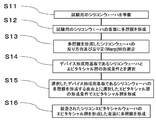
- FIG. 1 is a flowchart showing an example of a semiconductor device manufacturing method using a silicon epitaxial wafer manufactured by the silicon epitaxial wafer manufacturing method of the present invention.
- This multilayer film is preferably a multilayer film in which SiO 2 films and SiN films are alternately stacked, or a multilayer film in which SiO 2 films and polysilicon (poly-Si) films are alternately stacked.
- a process of measuring the warping direction and warping amount (Warp) W of the silicon wafer on which the multilayer film is formed is performed (see step S13 in FIG. 1).
- the warping direction of the silicon wafer on which the multilayer film is formed the case of forming a concave warp in which the multilayer film side is concave is defined as a concave shape, and the convex warpage in which the multilayer film side is convex is illustrated.
- the case where it is formed is described as a convex shape.
- a warp that offsets the warp amount W measured in a direction opposite to the measured warp direction is formed on the silicon wafer that is the device forming substrate and the silicon wafer that is the device forming substrate.
- Epitaxial layer formation conditions are selected (see step S14 in FIG. 1).
- warpage after film formation can be reduced by using a wafer having a shape that is opposite to the warpage in the process.
- the initial state of the wafer (silicon epitaxial wafer) to be used is a convex shape opposite to the concave shape (that is, a convex shape where the epitaxial layer side is a convex shape) To form a warp).
- a silicon wafer doped with phosphorus or boron as the silicon wafer as the device forming substrate.
- the lattice constant of the epitaxial layer usually resistivity
- the lattice constant of the silicon wafer doped with boron A misfit occurs in the middle, and film stress is generated in the epitaxial layer, and the silicon epitaxial wafer forms a warp such that the epitaxial layer side has a convex shape.
- boron has a smaller covalent bond radius than silicon, it is known that the epitaxial layer side of a silicon epitaxial wafer using a silicon wafer doped with boron at a high concentration warps in a convex shape.
- the initial state of the wafer to be used is made concave (that is, a concave warp in which the epitaxial layer side is concave) is formed, so that the warp during the process Defects can be reduced.
- a concave warp where the epitaxial layer side is concave on the silicon epitaxial wafer use a silicon wafer that is heavily doped with an element having a larger covalent bond radius than silicon as the silicon wafer that is the device forming substrate. Can be realized.
- the warpage amount of the warp formed on the silicon epitaxial wafer is the warpage amount W.
- W is a positive value
- the silicon wafer on which the multilayer film is formed is In the case of forming a convex warp having a convex shape on the film side, W is a negative value.
- the conditions of the silicon wafer as the device forming substrate and the formation conditions of the epitaxial layer are as follows: It is preferable to determine from the formula.
- W ⁇ (3 ⁇ l 2 ⁇ h f ) / (4 ⁇ h s 2 ) ⁇ ⁇ ⁇ (r Si ⁇ r X ) / r Si ⁇ ⁇ [X] / N S l: Diameter of a silicon wafer which is the device forming substrate, h f : thickness of the epitaxial layer, h s : thickness of the silicon wafer that is the device forming substrate, r Si : covalent bond radius of Si, r X : covalent bond radius of the element doped into the silicon wafer as the device forming substrate, N S : atomic density of Si, [X]: Dope concentration of an element doped into the silicon wafer that is the device forming substrate.
- the above formula can be derived by calculating the following formula.
- l, h s , and h f are the same as above, and ⁇ f and MSi are represented by the following formula.
- M Si is represented by the following formula.
- E Si represents the Young's modulus of Si
- ⁇ Si represents the Poisson's ratio of Si.
- the warpage amount of the warp formed on the silicon epitaxial wafer is desirably the same as the warp amount W, a multilayer film is formed on the surface of the silicon epitaxial wafer on which the epitaxial layer is formed even if it is not completely the same. If the warpage at the time can be offset and reduced, and the warpage when the multilayer film is formed can be improved, the yield in the device process can be improved.
- a process of forming an epitaxial layer on the surface for forming a multilayer film of a silicon wafer, which is the selected device forming substrate, under the selected epitaxial layer forming conditions is performed (see step S15 in FIG. 1), and the silicon epitaxial wafer is formed.
- the composition of the epitaxial layer to be formed can be, for example, silicon.
- a multilayer film is formed on the surface of the manufactured silicon epitaxial wafer on which the epitaxial layer is formed (see step S16 in FIG. 1).
- the multilayer film formed on the epitaxial layer may be the same multilayer film as that formed on the surface of the test silicon wafer in step S12.
- a semiconductor device can be manufactured as described above.
- a silicon epitaxial wafer in which warpage when a multilayer film is formed can be manufactured.
- the method for manufacturing a semiconductor device according to the present invention can reduce warpage when a multilayer film is formed on the surface of the epitaxial layer of a silicon epitaxial wafer, the subsequent process can be performed with a small amount of warpage. As a result, a semiconductor device can be manufactured without device failure.
- SiO 2 + SiN films 1 to 20 sets of “SiO 2 + SiN” films were laminated on the silicon wafer for testing.
- the film forming conditions for each film were the conditions imitating an actual process.
- the SiO 2 film was formed by TEOS (deposition temperature 380 ° C.), and the SiN film was formed by low pressure CVD (SiH 4 : 40 sccm, NH 3 : 2000 sccm, pressure 250 to 300 torr). All layers had a thickness of 25 nm.
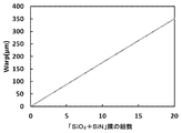
- Warp after the film formation was evaluated by a capacitance type measuring instrument and is shown in FIG. As shown in FIG. 3, as a result, Warp increased as the number of “SiO 2 + SiN” films to be stacked increased. Further, the shape of the silicon wafer on which the “SiO 2 + SiN” film was laminated was a shape in which the “SiO 2 + SiN” film side was concave.
- the conditions of the silicon wafer as the device forming substrate and the formation conditions of the epitaxial layer are estimated from the following equations so that a warp that offsets the measured Warp amount is formed in a direction opposite to the measured warp direction. It was. Note that a silicon wafer doped with boron was used as the silicon wafer as the device forming substrate. Silicon epitaxial wafers using silicon wafers with a high concentration of boron as the device formation substrate silicon wafers have a convex shape on the epitaxial layer side due to lattice mismatch between the silicon wafer with boron and the epitaxial layer. Therefore, the amount of warpage when the multilayer structure of the “SiO 2 + SiN” film described above is formed can be reduced.
- W ⁇ (3 ⁇ l 2 ⁇ h f ) / (4 ⁇ h s 2 ) ⁇ ⁇ ⁇ (r Si ⁇ r X ) / r Si ⁇ ⁇ [X] / N S l: Diameter of a silicon wafer which is the device forming substrate, h f : thickness of the epitaxial layer, h s : thickness of the silicon wafer that is the device forming substrate, r Si : covalent bond radius of Si, r X : covalent bond radius of the element doped into the silicon wafer as the device forming substrate, N S : atomic density of Si, [X]: Dope concentration of an element doped into the silicon wafer that is the device forming substrate.
- the conditions of the silicon wafer which is a device forming substrate for canceling Warp of about 280 ⁇ m when 16 sets of “SiO 2 + SiN” films are laminated, and the formation conditions of the epitaxial layer were calculated from the above formulas.
- W 280 ⁇ m was substituted into the above equation, and the variables were the substrate boron doping concentration ([X]) and the thickness of the epitaxial layer (h f ). Other factors were set to l: 300 mm, h s : 775 ⁇ m, r Si : 1.17 ⁇ , r X : 0.88 N, N S : 5 ⁇ 10 22 atoms / cm 3 .
- the relationship between the substrate boron doping concentration and the thickness of the epitaxial layer in this case is shown in FIG.
- the silicon epitaxial wafer manufactured under these conditions can cancel the warp that occurs when 16 sets of “SiO 2 + SiN” films are stacked on the epitaxial layer.
- the conditions of the silicon wafer, which is a device forming substrate for canceling Warp (W 420 ⁇ m) corresponding to the case where 24 sets of “SiO 2 + SiN” films are laminated, and the formation conditions of the epitaxial layer are also l, h s. , r Si, r X, the value of N S perform calculations the same value as above, also shown in FIG. 4 the relationship between the thickness of the substrate doped with boron concentration and the epitaxial layer.
- the thickness of the epitaxial layer (h f ) is set to 5 ⁇ m, and the substrate boron doping concentration ([X]) is set to 1 ⁇ 10 20 atoms / cm 3.
- An epitaxial layer was formed under the epitaxial layer formation conditions selected on the surface on which the multilayer film of the silicon wafer as the forming substrate was formed, and a silicon epitaxial wafer was manufactured.
- the composition of the epitaxial layer was silicon.
- the “SiO 2 + SiN” film is formed on the epitaxial layer of the silicon epitaxial wafer manufactured as described above, and the relationship between the number of the formed “SiO 2 + SiN” films and the Warp value of the silicon epitaxial wafer is shown in FIG. It was shown to.
- the Warp value in FIG. 5 is negative, the warp shape of the silicon epitaxial wafer indicates that the epitaxial layer side is convex, and when it is positive, the warp shape of the silicon epitaxial wafer is epitaxial. It shows that the layer side is concave.
- Example 2 A silicon epitaxial wafer was manufactured in the same manner as in Example 1 except that the thickness (h f ) of the epitaxial layer was 10 ⁇ m and the substrate boron doping concentration ([X]) was 5 ⁇ 10 19 atoms / cm 3. A “SiO 2 + SiN” film was formed thereon. The relationship between the number of “SiO 2 + SiN” films formed and the Warp value of the silicon epitaxial wafer is shown in FIG.
- the conditions of Examples 1 to 3 are conditions that can cancel the warpage when 16 sets of “SiO 2 + SiN” films are stacked. In fact, as shown in FIG. 5, it was found that the Warp was almost zero when 16 sets of “SiO 2 + SiN” films were laminated in the silicon epitaxial wafer manufactured under any of the conditions of Examples 1 to 3. . Note that three graphs showing the relationship between the number of “SiO 2 + SiN” films and the value of Warp in Examples 1 to 3 overlap as shown in FIG.
- the present invention is not limited to the above embodiment.
- the above-described embodiment is an exemplification, and the present invention has any configuration that has substantially the same configuration as the technical idea described in the claims of the present invention and that exhibits the same effects. Are included in the technical scope.
Landscapes
- Recrystallisation Techniques (AREA)
- Chemical & Material Sciences (AREA)
- Chemical Kinetics & Catalysis (AREA)
- Engineering & Computer Science (AREA)
- Manufacturing & Machinery (AREA)
Abstract
本発明は、予め、試験用のシリコンウェーハを準備し、該試験用のシリコンウェーハの表面に前記多層膜を形成し、該多層膜を形成したシリコンウェーハの反り方向及び反り量(Warp)Wを測定する工程と、前記測定した反り方向とは反対方向に前記測定した反り量Wを相殺する反りが形成されるように、デバイス形成用基板であるシリコンウェーハと該デバイス形成用基板であるシリコンウェーハ上に形成するエピタキシャル層の形成条件とを選択し、前記選択したデバイス形成用基板であるシリコンウェーハの前記多層膜を形成する表面上に前記選択したエピタキシャル層の形成条件で前記エピタキシャル層を形成する工程を含むシリコンエピタキシャルウェーハの製造方法である。これにより、多層膜を形成したときの反りが低減されるシリコンエピタキシャルウェーハを製造することができるシリコンエピタキシャルウェーハの製造方法が提供される。
Description
本発明は、シリコンエピタキシャルウェーハの製造方法及び半導体デバイスの製造方法に関する。
半導体集積回路を作製するための基板として、主にCZ(Czochralski)法によって作製されたシリコンウェーハが用いられている。近年の最先端メモリー素子では、大容量化とビットコスト低減のためにシリコンウェーハ上に多層膜を積層するプロセスを有する3次元構造のNANDフラッシュメモリーが使用されている。プロセスの比較的初期段階に「SiO2+SiN」膜を数十組積層する工程がある。積層後は、基板まで円柱形にエッチングを行うホールエッチング工程や、ポリシリコンを側壁に成膜する工程、SiNをエッチングする工程、電極形成工程等、3次元的で複雑な工程が多数あり、ウェーハが大きく反った状態で各工程を実施することは不良の原因となる。
特許文献1の請求項8には、反対方向に湾曲させた状態で、基板の一方の主表面上に薄膜を成膜させることが記載されている。しかし、当該先行技術では、湾曲させるために、エッチングを行っている。エッチングによる反り量の制御は、エッチング速度を同心円状に一定にする必要があり、成膜による反りを打ち消すような同心円状の反り形状を作りこむことは難しい。
また、特許文献2にはエピタキシャルウェーハの反りを予め識別して、基板の反りの方向をエピタキシャルウェーハ成長で生じる反り変化の方向と逆向きの方向に揃えて、エピタキシャルシリコンウェーハの反りの絶対値を低減することが記載されている。この先行技術では、基板となるシリコンウェーハの凹凸形状を選別することで、格子不整合による反りを低減することを目的としているが、数百μmの大きさの反り量(Warp)を低減させることは難しい。
図2は、3D-NANDデバイスのプロセスにおいてシリコンウェーハ(シリコン基板)上に多層膜が積層された状態を示す模式図である。多層膜が積層されたシリコンウェーハ1では、シリコンウェーハ(シリコン基板)2上に、SiO2膜3とSiN膜又はポリシリコン膜4とが交互にこの順に積層され、SiO2膜3とSiN膜又はポリシリコン膜4とからなる1組の「SiO2+SiN」膜又は「SiO2+ポリシリコン」膜5が複数組積層された多層膜6が積層(形成)されている。なお、図2中の点線の四角で囲まれた部分は、複数組積層された「SiO2+SiN」膜又は「SiO2+ポリシリコン」膜5のうち、その一部を省略したものである。
このように、3D-NANDデバイスのプロセスでは、プロセス初期段階に、「SiO2+SiN」膜や「SiO2+ポリシリコン」膜等の薄膜を何層も堆積させる工程が存在する。
その工程では、各種薄膜の膜厚や基板であるSiと膜材料の線膨張率の差、成膜時の真性応力等によりウェーハが大きく反ることがわかっている。その後のプロセスは、反りの大きな状態で行われるため、デバイス不良の原因となることがある。
本発明は、上記課題を解決するためになされたものであり、多層膜を形成したときの反りが低減されるシリコンエピタキシャルウェーハを製造することができるシリコンエピタキシャルウェーハの製造方法を提供することを目的とする。
上記課題を解決するために、本発明では、
シリコンウェーハと、該シリコンウェーハ上に形成されたエピタキシャル層からなり、前記エピタキシャル層上に多層膜を形成するためのシリコンエピタキシャルウェーハの製造方法であって、
予め、試験用のシリコンウェーハを準備し、該試験用のシリコンウェーハの表面に前記多層膜を形成し、該多層膜を形成したシリコンウェーハの反り方向及び反り量(Warp)Wを測定する工程と、
前記測定した反り方向とは反対方向に前記測定した反り量Wを相殺する反りが形成されるように、デバイス形成用基板であるシリコンウェーハと該デバイス形成用基板であるシリコンウェーハ上に形成するエピタキシャル層の形成条件とを選択し、前記選択したデバイス形成用基板であるシリコンウェーハの前記多層膜を形成する表面上に前記選択したエピタキシャル層の形成条件で前記エピタキシャル層を形成する工程を含むシリコンエピタキシャルウェーハの製造方法を提供する。
シリコンウェーハと、該シリコンウェーハ上に形成されたエピタキシャル層からなり、前記エピタキシャル層上に多層膜を形成するためのシリコンエピタキシャルウェーハの製造方法であって、
予め、試験用のシリコンウェーハを準備し、該試験用のシリコンウェーハの表面に前記多層膜を形成し、該多層膜を形成したシリコンウェーハの反り方向及び反り量(Warp)Wを測定する工程と、
前記測定した反り方向とは反対方向に前記測定した反り量Wを相殺する反りが形成されるように、デバイス形成用基板であるシリコンウェーハと該デバイス形成用基板であるシリコンウェーハ上に形成するエピタキシャル層の形成条件とを選択し、前記選択したデバイス形成用基板であるシリコンウェーハの前記多層膜を形成する表面上に前記選択したエピタキシャル層の形成条件で前記エピタキシャル層を形成する工程を含むシリコンエピタキシャルウェーハの製造方法を提供する。
このようなシリコンエピタキシャルウェーハの製造方法であれば、多層膜を形成したときの反りが低減されるシリコンエピタキシャルウェーハを製造することができる。
このとき、前記エピタキシャル層を形成する工程において、前記シリコンエピタキシャルウェーハに前記エピタキシャル層側が凹形状となる凹形状の反りを形成する場合は、前記デバイス形成用基板であるシリコンウェーハとして、ゲルマニウム又はスズがドープされたシリコンウェーハを用い、前記シリコンエピタキシャルウェーハに前記エピタキシャル層側が凸形状となる凸形状の反りを形成する場合は、前記デバイス形成用基板であるシリコンウェーハとして、リン又はボロンがドープされたシリコンウェーハを用いることが好ましい。
本発明の製造方法では、例えばこのような方法でデバイス形成用基板であるシリコンウェーハを選択することができる。
またこのとき、前記エピタキシャル層を形成する工程において、前記シリコンエピタキシャルウェーハに形成する反りの反り量が前記反り量W(ただし、前記多層膜を形成したシリコンウェーハが、前記多層膜側が凹形状となる凹形状の反りを形成する場合は、Wを正の値とし、前記多層膜を形成したシリコンウェーハが、前記多層膜側が凸形状となる凸形状の反りを形成する場合は、Wを負の値とする。)となるように、前記デバイス形成用基板であるシリコンウェーハの条件及び前記エピタキシャル層の形成条件を下記式より決定することが好ましい。
W={(3×l2×hf)/(4×hs 2)}×{(rSi-rX)/rSi}×[X]/NS
l:前記デバイス形成用基板であるシリコンウェーハの直径、
hf:前記エピタキシャル層の厚さ、
hs:前記デバイス形成用基板であるシリコンウェーハの厚さ、
rSi:Siの共有結合半径、
rX:前記デバイス形成用基板であるシリコンウェーハにドープする元素の共有結合半径、
NS:Siの原子密度、
[X]:前記デバイス形成用基板であるシリコンウェーハにドープする元素のドープ濃度。
W={(3×l2×hf)/(4×hs 2)}×{(rSi-rX)/rSi}×[X]/NS
l:前記デバイス形成用基板であるシリコンウェーハの直径、
hf:前記エピタキシャル層の厚さ、
hs:前記デバイス形成用基板であるシリコンウェーハの厚さ、
rSi:Siの共有結合半径、
rX:前記デバイス形成用基板であるシリコンウェーハにドープする元素の共有結合半径、
NS:Siの原子密度、
[X]:前記デバイス形成用基板であるシリコンウェーハにドープする元素のドープ濃度。
本発明では、デバイス形成用基板であるシリコンウェーハの条件及びエピタキシャル層の形成条件を、例えばこのような方法で決定することができる。
またこのとき、前記多層膜を、SiO2膜とSiN膜とが交互に積層された多層膜又はSiO2膜とポリシリコン膜とが交互に積層された多層膜とすることが好ましい。
本発明のシリコンエピタキシャルウェーハの製造方法では、多層膜をSiO2膜とSiN膜とが交互に積層された多層膜又はSiO2膜とポリシリコン膜とが交互に積層された多層膜とすることができる。
また、本発明では、上述のシリコンエピタキシャルウェーハの製造方法で製造されたシリコンエピタキシャルウェーハの前記エピタキシャル層を形成した表面に前記多層膜を形成する半導体デバイスの製造方法を提供する。
本発明の半導体デバイスの製造方法であれば、シリコンエピタキシャルウェーハのエピタキシャル層を形成した表面に多層膜を形成したときの反りを低減させることができることから、その後のプロセスは反りが小さな状態で行われるため、デバイス不良が起きることなく半導体デバイスを製造することができる。
本発明のシリコンエピタキシャルウェーハの製造方法であれば、多層膜を形成したときの反りが低減されるシリコンエピタキシャルウェーハを製造することができる。また、本発明の半導体デバイスの製造方法であれば、シリコンエピタキシャルウェーハのエピタキシャル層を形成した表面に多層膜を形成したときの反りを低減させることができることから、その後のプロセスは反りが小さな状態で行われるため、デバイス不良が起きることなく半導体デバイスを製造することができる。
以下、本発明について図面を参照して詳細に説明するが、本発明はこれらに限定されるものではない。
本発明は、シリコンウェーハと、該シリコンウェーハ上に形成されたエピタキシャル層からなり、前記エピタキシャル層上に多層膜を形成するためのシリコンエピタキシャルウェーハの製造方法である。本発明のシリコンエピタキシャルウェーハの製造方法は、予め、試験用のシリコンウェーハを準備し、該試験用のシリコンウェーハの表面に前記多層膜を形成し、該多層膜を形成したシリコンウェーハの反り方向及び反り量(Warp)Wを測定する工程と、前記測定した反り方向とは反対方向に前記測定した反り量Wを相殺する反りが形成されるように、デバイス形成用基板であるシリコンウェーハと該デバイス形成用基板であるシリコンウェーハ上に形成するエピタキシャル層の形成条件とを選択し、前記選択したデバイス形成用基板であるシリコンウェーハの前記多層膜を形成する表面上に前記選択したエピタキシャル層の形成条件で前記エピタキシャル層を形成する工程を含む。以下、本発明のシリコンエピタキシャルウェーハの製造方法についてより詳細に説明する。
図1は、本発明のシリコンエピタキシャルウェーハの製造方法によって製造されたシリコンエピタキシャルウェーハを用いた半導体デバイスの製造方法の一例を示すフロー図である。
まず、予め、試験用のシリコンウェーハを準備する(図1のステップS11参照)。この試験用のシリコンウェーハとしては、特に限定されないが、後述する反り量(Warp)Wを容易に測定できるように、反りの少ない(例えば、Warpが数μm程度と非常に小さい)シリコンウェーハを用いることが好ましい。
次に、試験用のシリコンウェーハの表面に多層膜を形成する(図1のステップS12参照)。この多層膜は、SiO2膜とSiN膜とが交互に積層された多層膜又はSiO2膜とポリシリコン(poly-Si)膜とが交互に積層された多層膜とすることが好ましい。
その後、多層膜を形成したシリコンウェーハの反り方向及び反り量(Warp)Wを測定する工程を行う(図1のステップS13参照)。なお、以下では、多層膜を形成したシリコンウェーハの反り方向については、多層膜側が凹形状となる凹形状の反りを形成する場合を凹形状とし、多層膜側が凸形状となる凸形状の反りを形成する場合を凸形状として説明を行う。
この後、測定した反り方向とは反対方向に測定した反り量Wを相殺する反りが形成されるように、デバイス形成用基板であるシリコンウェーハと該デバイス形成用基板であるシリコンウェーハ上に形成するエピタキシャル層の形成条件とを選択する(図1のステップS14参照)。
このとき選択するデバイス形成用基板であるシリコンウェーハとしては、例えば、シリコンとは共有結合半径が異なる元素がドープされたシリコンウェーハを選択すればよい。
多層プロセスでの反りによる不良を低減するためには、プロセスでの反りとは逆の形状に反ったウェーハを用いることで、成膜後の反りを低減できる。具体的には、プロセスでの反りが凹形状であれば、使用するウェーハ(シリコンエピタキシャルウェーハ)の初期状態を凹形状とは逆の凸形状にする(即ち、エピタキシャル層側が凸形状となる凸形状の反りを形成する)ということである。シリコンエピタキシャルウェーハにエピタキシャル層側が凸形状となる凸形状の反りを形成する場合は、デバイス形成用基板であるシリコンウェーハとして、リン又はボロンがドープされたシリコンウェーハを用いることが好ましい。例えば、デバイス形成用基板であるシリコンウェーハとして、ボロンが高濃度にドープされたシリコンウェーハを用いることで、エピタキシャル層(通常抵抗率)の格子定数とボロンがドープされたシリコンウェーハの格子定数との間にミスフィットが生じ、エピタキシャル層に膜応力が発生し、シリコンエピタキシャルウェーハは、エピタキシャル層側が凸形状となるような反りを形成する。ボロンはシリコンよりも共有結合半径が小さいことから、ボロンを高濃度に添加したシリコンウェーハを用いたシリコンエピタキシャルウェーハは、エピタキシャル層側が凸形状に反ることがわかっている。
他方、多層プロセスでの反りが凸形状であれば、使用するウェーハの初期状態を凹形状にする(即ち、エピタキシャル層側が凹形状となる凹形状の反りを形成する)ことで、プロセス中の反り不良を低減できる。シリコンエピタキシャルウェーハにエピタキシャル層側が凹形状となる凹形状の反りを形成する場合は、デバイス形成用基板であるシリコンウェーハとして、シリコンよりも共有結合半径の大きい元素を多量にドープしたシリコンウェーハを用いることで実現できる。例えば、デバイス形成用基板であるシリコンウェーハとして、ゲルマニウム又はスズがドープされたシリコンウェーハを用いることが好ましい。
なお、デバイス形成用基板であるシリコンウェーハと該デバイス形成用基板であるシリコンウェーハ上に形成するエピタキシャル層の形成条件とを選択するにあたり、シリコンエピタキシャルウェーハに形成する反りの反り量が前記反り量W(ただし、前記多層膜を形成したシリコンウェーハが、前記多層膜側が凹形状となる凹形状の反りを形成する場合は、Wを正の値とし、前記多層膜を形成したシリコンウェーハが、前記多層膜側が凸形状となる凸形状の反りを形成する場合は、Wを負の値とする。)となるように、前記デバイス形成用基板であるシリコンウェーハの条件及び前記エピタキシャル層の形成条件を下記式より決定することが好ましい。
W={(3×l2×hf)/(4×hs 2)}×{(rSi-rX)/rSi}×[X]/NS
l:前記デバイス形成用基板であるシリコンウェーハの直径、
hf:前記エピタキシャル層の厚さ、
hs:前記デバイス形成用基板であるシリコンウェーハの厚さ、
rSi:Siの共有結合半径、
rX:前記デバイス形成用基板であるシリコンウェーハにドープする元素の共有結合半径、
NS:Siの原子密度、
[X]:前記デバイス形成用基板であるシリコンウェーハにドープする元素のドープ濃度。
W={(3×l2×hf)/(4×hs 2)}×{(rSi-rX)/rSi}×[X]/NS
l:前記デバイス形成用基板であるシリコンウェーハの直径、
hf:前記エピタキシャル層の厚さ、
hs:前記デバイス形成用基板であるシリコンウェーハの厚さ、
rSi:Siの共有結合半径、
rX:前記デバイス形成用基板であるシリコンウェーハにドープする元素の共有結合半径、
NS:Siの原子密度、
[X]:前記デバイス形成用基板であるシリコンウェーハにドープする元素のドープ濃度。
上記式を用いて、デバイス形成用基板であるシリコンウェーハの条件及びエピタキシャル層の形成条件を決定する方法としては、特に限定されないが、例えば、測定した反り量Wを上記式に代入し、上記式中のl,hs,rSi,rX,及びNSを定数とし、hf(エピタキシャル層の厚さ)と[X](デバイス形成用基板であるシリコンウェーハにドープする元素のドープ濃度)を変数として上記条件を決定する方法が挙げられる。この場合、エピタキシャル層の厚さが厚くなるほど、デバイス形成用基板であるシリコンウェーハにドープする元素のドープ濃度は低くなる関係となる。
なお、上記式は、下記式を計算することによって導出することができる。

(式中、l,hs,及びhfは上記と同様であり、σf及びMSiは下記式で表される。)
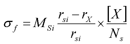
(式中、rSi,rX,[X],及びNSは上記と同様であり、MSiは下記式で表される。)
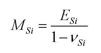
(式中、ESiはSiのヤング率を示し、νSiはSiのポアソン比を示す。)
なお、シリコンエピタキシャルウェーハに形成する反りの反り量は前記反り量Wと同一にするのが望ましいが、完全に同一にならなくとも、シリコンエピタキシャルウェーハのエピタキシャル層を形成した表面に多層膜を形成したときの反りを相殺して低減し、多層膜を形成したときの反りを改善することができれば、デバイス工程における歩留りの向上を計ることができる。
次に、選択したデバイス形成用基板であるシリコンウェーハの多層膜を形成する表面上に選択したエピタキシャル層の形成条件でエピタキシャル層を形成する工程を行い(図1のステップS15参照)、シリコンエピタキシャルウェーハを製造する。形成するエピタキシャル層の組成は、例えばシリコンとすることができる。
その後、製造されたシリコンエピタキシャルウェーハのエピタキシャル層を形成した表面に多層膜を形成する(図1のステップS16参照)。エピタキシャル層上に形成する多層膜としては、ステップS12において試験用のシリコンウェーハの表面に形成した多層膜と同じ多層膜とすればよい。
上記のようにして半導体デバイスを製造することができる。
以上説明したように、本発明のシリコンエピタキシャルウェーハの製造方法であれば、多層膜を形成したときの反りが低減されるシリコンエピタキシャルウェーハを製造することができる。また、本発明の半導体デバイスの製造方法であれば、シリコンエピタキシャルウェーハのエピタキシャル層を形成した表面に多層膜を形成したときの反りを低減させることができることから、その後のプロセスは反りが小さな状態で行われるため、デバイス不良が起きることなく半導体デバイスを製造することができる。
以下、実施例を示して本発明をより具体的に説明するが、本発明はこれらに限定されるものではない。
(実施例1)
まず、試験用のシリコンウェーハ(エピタキシャル層は形成されていない。)を用いて、3D-NANDデバイスにおける最初の積層工程である「SiO2+SiN」膜の積層工程(多層膜工程)での反り方向及び反り量を実測した。試験用のシリコンウェーハとしては、具体的には、Warpが非常に小さい(数μm)直径300mmのp型で抵抗率が10Ω・cmのシリコンウェーハを用いた。
まず、試験用のシリコンウェーハ(エピタキシャル層は形成されていない。)を用いて、3D-NANDデバイスにおける最初の積層工程である「SiO2+SiN」膜の積層工程(多層膜工程)での反り方向及び反り量を実測した。試験用のシリコンウェーハとしては、具体的には、Warpが非常に小さい(数μm)直径300mmのp型で抵抗率が10Ω・cmのシリコンウェーハを用いた。
この試験用のシリコンウェーハに「SiO2+SiN」膜を1~20組積層した。各膜の成膜条件は実際のプロセスを模した条件とした。SiO2膜はTEOS(成膜温度380℃)で成膜し、SiN膜は減圧CVDで成膜(SiH4:40sccm,NH3:2000sccm,圧力250~300torr)した。いずれの層も厚さは25nmであった。
次に、「SiO2+SiN」膜を積層したシリコンウェーハについて、成膜後のWarpを静電容量式の測定器で評価し、図3に示した。図3に示すように、結果として、Warpは積層する「SiO2+SiN」膜の組数が増えるに従って大きくなった。また、「SiO2+SiN」膜を積層したシリコンウェーハの形状は、「SiO2+SiN」膜側が凹形状となる形状となった。
そして、上記測定した反り方向とは反対方向で、上記測定したWarp量を相殺する反りが形成されるように、デバイス形成用基板であるシリコンウェーハの条件及びエピタキシャル層の形成条件を下記式から見積もった。なお、デバイス形成用基板であるシリコンウェーハとしては、ボロンをドープしたシリコンウェーハを用いることとした。デバイス形成用基板であるシリコンウェーハとして、ボロンを高濃度に添加したシリコンウェーハを用いたシリコンエピタキシャルウェーハは、ボロンを添加したシリコンウェーハとエピタキシャル層の格子不整合により、エピタキシャル層側が凸形状となるように反るため、上述した「SiO2+SiN」膜の多層膜構造を形成したときの反り量を低減することができる。
W={(3×l2×hf)/(4×hs 2)}×{(rSi-rX)/rSi}×[X]/NS
l:前記デバイス形成用基板であるシリコンウェーハの直径、
hf:前記エピタキシャル層の厚さ、
hs:前記デバイス形成用基板であるシリコンウェーハの厚さ、
rSi:Siの共有結合半径、
rX:前記デバイス形成用基板であるシリコンウェーハにドープする元素の共有結合半径、
NS:Siの原子密度、
[X]:前記デバイス形成用基板であるシリコンウェーハにドープする元素のドープ濃度。
W={(3×l2×hf)/(4×hs 2)}×{(rSi-rX)/rSi}×[X]/NS
l:前記デバイス形成用基板であるシリコンウェーハの直径、
hf:前記エピタキシャル層の厚さ、
hs:前記デバイス形成用基板であるシリコンウェーハの厚さ、
rSi:Siの共有結合半径、
rX:前記デバイス形成用基板であるシリコンウェーハにドープする元素の共有結合半径、
NS:Siの原子密度、
[X]:前記デバイス形成用基板であるシリコンウェーハにドープする元素のドープ濃度。
次に、「SiO2+SiN」膜を16組積層した場合のWarp約280μmを打ち消すためのデバイス形成用基板であるシリコンウェーハの条件及びエピタキシャル層の形成条件を上記式から算出した。上記式にW=280μmを代入し、変数は、基板ボロンドープ濃度([X])とエピタキシャル層の厚さ(hf)とした。また、その他の因子はl:300mm、hs:775μm、rSi:1.17Å、rX:0.88Å、NS:5×10²²atoms/cm3とした。この場合における基板ボロンドープ濃度とエピタキシャル層の厚さとの関係を図4に示した。この場合、エピタキシャル層の厚さが厚いほど、基板にドープしなければいけないボロンの濃度は低くなる。この条件で製造されたシリコンエピタキシャルウェーハは、エピタキシャル層上に「SiO2+SiN」膜を16組積層した場合に生じる反りを打ち消すことができる。なお、「SiO2+SiN」膜を24組積層した場合に相当するWarp(W=420μm)を打ち消すためのデバイス形成用基板であるシリコンウェーハの条件及びエピタキシャル層の形成条件についても、l、hs、rSi、rX、NSの値を上記と同じ値として計算を行い、基板ボロンドープ濃度とエピタキシャル層の厚さとの関係について図4に併せて示した。
図4中のW=280μmの場合のグラフに基づいて、エピタキシャル層の厚さ(hf)を5μmとし、基板ボロンドープ濃度([X])を1×10²⁰atoms/cm3として、選択したデバイス形成用基板であるシリコンウェーハの多層膜を形成する表面上に選択したエピタキシャル層の形成条件でエピタキシャル層の形成を行い、シリコンエピタキシャルウェーハを製造した。なお、エピタキシャル層の組成は、シリコンとした。
上記のように製造されたシリコンエピタキシャルウェーハのエピタキシャル層上に「SiO2+SiN」膜を形成し、形成した「SiO2+SiN」膜の組数とシリコンエピタキシャルウェーハのWarpの値との関係を図5に示した。なお、図5中のWarpの値がマイナスの場合は、シリコンエピタキシャルウェーハの反りの形状がエピタキシャル層側が凸形状となっていることを示し、プラスの場合は、シリコンエピタキシャルウェーハの反りの形状がエピタキシャル層側が凹形状となっていることを示す。
(実施例2)
エピタキシャル層の厚さ(hf)を10μmとし、基板ボロンドープ濃度([X])を5×10¹⁹atoms/cm3とした以外は実施例1と同様にしてシリコンエピタキシャルウェーハを製造し、エピタキシャル層上に「SiO2+SiN」膜を形成した。形成した「SiO2+SiN」膜の組数とシリコンエピタキシャルウェーハのWarpの値との関係を図5に示した。
エピタキシャル層の厚さ(hf)を10μmとし、基板ボロンドープ濃度([X])を5×10¹⁹atoms/cm3とした以外は実施例1と同様にしてシリコンエピタキシャルウェーハを製造し、エピタキシャル層上に「SiO2+SiN」膜を形成した。形成した「SiO2+SiN」膜の組数とシリコンエピタキシャルウェーハのWarpの値との関係を図5に示した。
(実施例3)
エピタキシャル層の厚さ(hf)を15μmとし、基板ボロンドープ濃度([X])を3×10¹⁹atoms/cm3とした以外は実施例1と同様にしてシリコンエピタキシャルウェーハを製造し、エピタキシャル層上に「SiO2+SiN」膜を形成した。形成した「SiO2+SiN」膜の組数とシリコンエピタキシャルウェーハのWarpの値との関係を図5に示した。
エピタキシャル層の厚さ(hf)を15μmとし、基板ボロンドープ濃度([X])を3×10¹⁹atoms/cm3とした以外は実施例1と同様にしてシリコンエピタキシャルウェーハを製造し、エピタキシャル層上に「SiO2+SiN」膜を形成した。形成した「SiO2+SiN」膜の組数とシリコンエピタキシャルウェーハのWarpの値との関係を図5に示した。
実施例1~3の条件はいずれも「SiO2+SiN」膜を16組積層した場合に反りを打ち消すことができる条件である。実際、図5に示されるように、実施例1~3のいずれの条件で製造されたシリコンエピタキシャルウェーハも、「SiO2+SiN」膜を16組積層した時にWarpがほぼ0になることが分かった。なお、実施例1~3における「SiO2+SiN」膜の組数とWarpの値との関係を示す3つのグラフは、図5に示す通り重なっている。
なお、本発明は、上記実施形態に限定されるものではない。上記実施形態は例示であり、本発明の特許請求の範囲に記載された技術的思想と実質的に同一な構成を有し、同様な作用効果を奏するものは、いかなるものであっても本発明の技術的範囲に包含される。
Claims (5)
- シリコンウェーハと、該シリコンウェーハ上に形成されたエピタキシャル層からなり、前記エピタキシャル層上に多層膜を形成するためのシリコンエピタキシャルウェーハの製造方法であって、
予め、試験用のシリコンウェーハを準備し、該試験用のシリコンウェーハの表面に前記多層膜を形成し、該多層膜を形成したシリコンウェーハの反り方向及び反り量(Warp)Wを測定する工程と、
前記測定した反り方向とは反対方向に前記測定した反り量Wを相殺する反りが形成されるように、デバイス形成用基板であるシリコンウェーハと該デバイス形成用基板であるシリコンウェーハ上に形成するエピタキシャル層の形成条件とを選択し、前記選択したデバイス形成用基板であるシリコンウェーハの前記多層膜を形成する表面上に前記選択したエピタキシャル層の形成条件で前記エピタキシャル層を形成する工程を含むことを特徴とするシリコンエピタキシャルウェーハの製造方法。 - 前記エピタキシャル層を形成する工程において、前記シリコンエピタキシャルウェーハに前記エピタキシャル層側が凹形状となる凹形状の反りを形成する場合は、前記デバイス形成用基板であるシリコンウェーハとして、ゲルマニウム又はスズがドープされたシリコンウェーハを用い、前記シリコンエピタキシャルウェーハに前記エピタキシャル層側が凸形状となる凸形状の反りを形成する場合は、前記デバイス形成用基板であるシリコンウェーハとして、リン又はボロンがドープされたシリコンウェーハを用いることを特徴とする請求項1に記載のシリコンエピタキシャルウェーハの製造方法。
- 前記エピタキシャル層を形成する工程において、前記シリコンエピタキシャルウェーハに形成する反りの反り量が前記反り量W(ただし、前記多層膜を形成したシリコンウェーハが、前記多層膜側が凹形状となる凹形状の反りを形成する場合は、Wを正の値とし、前記多層膜を形成したシリコンウェーハが、前記多層膜側が凸形状となる凸形状の反りを形成する場合は、Wを負の値とする。)となるように、前記デバイス形成用基板であるシリコンウェーハの条件及び前記エピタキシャル層の形成条件を下記式より決定することを特徴とする請求項1又は請求項2に記載のシリコンエピタキシャルウェーハの製造方法。
W={(3×l2×hf)/(4×hs 2)}×{(rSi-rX)/rSi}×[X]/NS
l:前記デバイス形成用基板であるシリコンウェーハの直径、
hf:前記エピタキシャル層の厚さ、
hs:前記デバイス形成用基板であるシリコンウェーハの厚さ、
rSi:Siの共有結合半径、
rX:前記デバイス形成用基板であるシリコンウェーハにドープする元素の共有結合半径、
NS:Siの原子密度、
[X]:前記デバイス形成用基板であるシリコンウェーハにドープする元素のドープ濃度。 - 前記多層膜を、SiO2膜とSiN膜とが交互に積層された多層膜又はSiO2膜とポリシリコン膜とが交互に積層された多層膜とすることを特徴とする請求項1から請求項3のいずれか一項に記載のシリコンエピタキシャルウェーハの製造方法。
- 請求項1から請求項4のいずれか一項に記載のシリコンエピタキシャルウェーハの製造方法で製造されたシリコンエピタキシャルウェーハの前記エピタキシャル層を形成した表面に前記多層膜を形成することを特徴とする半導体デバイスの製造方法。
Priority Applications (3)
| Application Number | Priority Date | Filing Date | Title |
|---|---|---|---|
| CN201780055108.2A CN109690738B (zh) | 2016-09-07 | 2017-08-17 | 外延硅晶片的制造方法及半导体器件的制造方法 |
| KR1020197005933A KR102352511B1 (ko) | 2016-09-07 | 2017-08-17 | 실리콘에피택셜 웨이퍼의 제조방법 및 반도체 디바이스의 제조방법 |
| US16/326,832 US10734220B2 (en) | 2016-09-07 | 2017-08-17 | Method for manufacturing silicon epitaxial wafer and method for manufacturing semiconductor device |
Applications Claiming Priority (2)
| Application Number | Priority Date | Filing Date | Title |
|---|---|---|---|
| JP2016174640A JP6662250B2 (ja) | 2016-09-07 | 2016-09-07 | シリコンエピタキシャルウェーハの製造方法及び半導体デバイスの製造方法 |
| JP2016-174640 | 2016-09-07 |
Publications (1)
| Publication Number | Publication Date |
|---|---|
| WO2018047595A1 true WO2018047595A1 (ja) | 2018-03-15 |
Family
ID=61562099
Family Applications (1)
| Application Number | Title | Priority Date | Filing Date |
|---|---|---|---|
| PCT/JP2017/029484 Ceased WO2018047595A1 (ja) | 2016-09-07 | 2017-08-17 | シリコンエピタキシャルウェーハの製造方法及び半導体デバイスの製造方法 |
Country Status (5)
| Country | Link |
|---|---|
| US (1) | US10734220B2 (ja) |
| JP (1) | JP6662250B2 (ja) |
| KR (1) | KR102352511B1 (ja) |
| CN (1) | CN109690738B (ja) |
| WO (1) | WO2018047595A1 (ja) |
Families Citing this family (2)
| Publication number | Priority date | Publication date | Assignee | Title |
|---|---|---|---|---|
| FR3064398B1 (fr) * | 2017-03-21 | 2019-06-07 | Soitec | Structure de type semi-conducteur sur isolant, notamment pour un capteur d'image de type face avant, et procede de fabrication d'une telle structure |
| US12613197B2 (en) * | 2019-12-03 | 2026-04-28 | Kla Corporation | Low-reflectivity back-illuminated image sensor |
Citations (5)
| Publication number | Priority date | Publication date | Assignee | Title |
|---|---|---|---|---|
| JPH06112120A (ja) * | 1992-09-26 | 1994-04-22 | Toshiba Corp | 半導体エピタキシャル基板の製造方法 |
| JPH07249573A (ja) * | 1994-03-14 | 1995-09-26 | Nippon Steel Corp | 半導体基板の製造方法 |
| JP2010080685A (ja) * | 2008-09-26 | 2010-04-08 | Toshiba Corp | 不揮発性記憶装置及びその製造方法 |
| JP2010118487A (ja) * | 2008-11-13 | 2010-05-27 | Shin Etsu Handotai Co Ltd | エピタキシャルウェーハの評価方法およびエピタキシャルウェーハの製造方法 |
| JP2014179656A (ja) * | 2010-10-14 | 2014-09-25 | Eugene Technology Co Ltd | 3次元構造のメモリ素子を製造する装置 |
Family Cites Families (10)
| Publication number | Priority date | Publication date | Assignee | Title |
|---|---|---|---|---|
| JPH08753B2 (ja) * | 1986-09-26 | 1996-01-10 | 徳三 助川 | シリコン素子用基板作製方法 |
| US4830984A (en) * | 1987-08-19 | 1989-05-16 | Texas Instruments Incorporated | Method for heteroepitaxial growth using tensioning layer on rear substrate surface |
| JP4569026B2 (ja) * | 2001-03-30 | 2010-10-27 | 信越半導体株式会社 | 半導体基板及びその製造方法 |
| JP4521327B2 (ja) * | 2005-07-19 | 2010-08-11 | 株式会社東芝 | 半導体装置の製造方法 |
| JP4984046B2 (ja) * | 2007-01-29 | 2012-07-25 | 信越半導体株式会社 | 気相成長用サセプタ及び気相成長装置並びに気相成長用サセプタの設計方法及び気相成長方法 |
| JP2009302163A (ja) | 2008-06-11 | 2009-12-24 | Sumco Corp | シリコンウェーハ及びそれを用いたエピタキシャルシリコンウェーハ及び貼り合わせsoiウェーハ並びにそれらの製造方法。 |
| JP5544986B2 (ja) * | 2010-04-01 | 2014-07-09 | 信越半導体株式会社 | 貼り合わせsoiウェーハの製造方法、及び貼り合わせsoiウェーハ |
| JP5418564B2 (ja) * | 2011-09-29 | 2014-02-19 | 信越半導体株式会社 | 貼り合わせsoiウェーハの反りを算出する方法、及び貼り合わせsoiウェーハの製造方法 |
| KR102003526B1 (ko) * | 2012-07-31 | 2019-07-25 | 삼성전자주식회사 | 반도체 메모리 소자 및 그 제조방법 |
| JP6166383B2 (ja) * | 2012-12-28 | 2017-07-19 | サンエディソン・セミコンダクター・リミテッドSunEdison Semiconductor Limited | エピタキシャル後反りの予測および制御方法 |
-
2016
- 2016-09-07 JP JP2016174640A patent/JP6662250B2/ja active Active
-
2017
- 2017-08-17 WO PCT/JP2017/029484 patent/WO2018047595A1/ja not_active Ceased
- 2017-08-17 KR KR1020197005933A patent/KR102352511B1/ko active Active
- 2017-08-17 CN CN201780055108.2A patent/CN109690738B/zh active Active
- 2017-08-17 US US16/326,832 patent/US10734220B2/en active Active
Patent Citations (5)
| Publication number | Priority date | Publication date | Assignee | Title |
|---|---|---|---|---|
| JPH06112120A (ja) * | 1992-09-26 | 1994-04-22 | Toshiba Corp | 半導体エピタキシャル基板の製造方法 |
| JPH07249573A (ja) * | 1994-03-14 | 1995-09-26 | Nippon Steel Corp | 半導体基板の製造方法 |
| JP2010080685A (ja) * | 2008-09-26 | 2010-04-08 | Toshiba Corp | 不揮発性記憶装置及びその製造方法 |
| JP2010118487A (ja) * | 2008-11-13 | 2010-05-27 | Shin Etsu Handotai Co Ltd | エピタキシャルウェーハの評価方法およびエピタキシャルウェーハの製造方法 |
| JP2014179656A (ja) * | 2010-10-14 | 2014-09-25 | Eugene Technology Co Ltd | 3次元構造のメモリ素子を製造する装置 |
Also Published As
| Publication number | Publication date |
|---|---|
| CN109690738B (zh) | 2023-05-23 |
| US20190228962A1 (en) | 2019-07-25 |
| CN109690738A (zh) | 2019-04-26 |
| KR20190045189A (ko) | 2019-05-02 |
| US10734220B2 (en) | 2020-08-04 |
| KR102352511B1 (ko) | 2022-01-18 |
| JP6662250B2 (ja) | 2020-03-11 |
| JP2018041829A (ja) | 2018-03-15 |
Similar Documents
| Publication | Publication Date | Title |
|---|---|---|
| US11501968B2 (en) | Method for providing a semiconductor device with silicon filled gaps | |
| JP6717267B2 (ja) | シリコンウェーハの製造方法 | |
| TWI766871B (zh) | 經由差排過濾形成磊晶層 | |
| JP6777029B2 (ja) | シリコンウェーハ及びその製造方法 | |
| US20090142925A1 (en) | Method for forming tungsten film having low resistivity and good surface roughness and method for forming wiring of semiconductor device using the same | |
| JP7711317B2 (ja) | 3色3d dramスタックおよび製作する方法 | |
| KR102477091B1 (ko) | 2차원 물질 하드마스크와 그 제조방법 및 하드 마스크를 이용한 물질층 패턴 형성방법 | |
| JP2018520510A5 (ja) | 多層構造体の製造方法 | |
| JPH08213327A (ja) | 半導体薄膜形成方法 | |
| WO2018047595A1 (ja) | シリコンエピタキシャルウェーハの製造方法及び半導体デバイスの製造方法 | |
| CN107731844A (zh) | 3d存储器的蚀刻方法 | |
| US9224749B1 (en) | Method for filling polysilicon gate in semiconductor devices, and semiconductor devices | |
| JP6434862B2 (ja) | 半導体装置の製造方法 | |
| JP2020150225A (ja) | 半導体装置の製造方法 | |
| CN111103767B (zh) | 一种半导体器件及其制作方法和电子设备 | |
| JPWO2022101969A5 (ja) | ||
| JP4943172B2 (ja) | シリコンエピタキシャル膜を有するsos基板の形成法 | |
| CN115939031A (zh) | 一种晶圆结构及其晶圆弯曲度的调控方法 | |
| CN112151511A (zh) | 一种半导体结构及其制备方法 | |
| CN114743974A (zh) | 多晶硅的沉积方法及接触插塞的制造方法 | |
| CN111164240B (zh) | 硅晶片 | |
| TW202014664A (zh) | 軟性基板之應變量測與應力優化之方法、裝置、回授系統與電腦可讀取記錄媒體 | |
| KR102156349B1 (ko) | 표면 스트레스가 완화된 결정질의 탄화실리콘 박막 구조체 제조방법 | |
| JP2009245968A (ja) | 半導体装置の製造方法 |
Legal Events
| Date | Code | Title | Description |
|---|---|---|---|
| 121 | Ep: the epo has been informed by wipo that ep was designated in this application |
Ref document number: 17848538 Country of ref document: EP Kind code of ref document: A1 |
|
| ENP | Entry into the national phase |
Ref document number: 20197005933 Country of ref document: KR Kind code of ref document: A |
|
| NENP | Non-entry into the national phase |
Ref country code: DE |
|
| 122 | Ep: pct application non-entry in european phase |
Ref document number: 17848538 Country of ref document: EP Kind code of ref document: A1 |