WO2018034103A1 - 積層型lcフィルタ - Google Patents
積層型lcフィルタ Download PDFInfo
- Publication number
- WO2018034103A1 WO2018034103A1 PCT/JP2017/026617 JP2017026617W WO2018034103A1 WO 2018034103 A1 WO2018034103 A1 WO 2018034103A1 JP 2017026617 W JP2017026617 W JP 2017026617W WO 2018034103 A1 WO2018034103 A1 WO 2018034103A1
- Authority
- WO
- WIPO (PCT)
- Prior art keywords
- resonators
- conductor pattern
- line
- capacitor
- multilayer
- Prior art date
- Legal status (The legal status is an assumption and is not a legal conclusion. Google has not performed a legal analysis and makes no representation as to the accuracy of the status listed.)
- Ceased
Links
Images


Classifications
-
- H—ELECTRICITY
- H03—ELECTRONIC CIRCUITRY
- H03H—IMPEDANCE NETWORKS, e.g. RESONANT CIRCUITS; RESONATORS
- H03H7/00—Multiple-port networks comprising only passive electrical elements as network components
- H03H7/01—Frequency selective two-port networks
- H03H7/0115—Frequency selective two-port networks comprising only inductors and capacitors
-
- H—ELECTRICITY
- H01—ELECTRIC ELEMENTS
- H01F—MAGNETS; INDUCTANCES; TRANSFORMERS; SELECTION OF MATERIALS FOR THEIR MAGNETIC PROPERTIES
- H01F17/00—Fixed inductances of the signal type
- H01F17/0006—Printed inductances
- H01F17/0013—Printed inductances with stacked layers
-
- H—ELECTRICITY
- H03—ELECTRONIC CIRCUITRY
- H03H—IMPEDANCE NETWORKS, e.g. RESONANT CIRCUITS; RESONATORS
- H03H1/00—Constructional details of impedance networks whose electrical mode of operation is not specified or applicable to more than one type of network
-
- H—ELECTRICITY
- H03—ELECTRONIC CIRCUITRY
- H03H—IMPEDANCE NETWORKS, e.g. RESONANT CIRCUITS; RESONATORS
- H03H7/00—Multiple-port networks comprising only passive electrical elements as network components
- H03H7/01—Frequency selective two-port networks
- H03H7/09—Filters comprising mutual inductance
-
- H—ELECTRICITY
- H03—ELECTRONIC CIRCUITRY
- H03H—IMPEDANCE NETWORKS, e.g. RESONANT CIRCUITS; RESONATORS
- H03H7/00—Multiple-port networks comprising only passive electrical elements as network components
- H03H7/01—Frequency selective two-port networks
- H03H7/17—Structural details of sub-circuits of frequency selective networks
- H03H7/1708—Comprising bridging elements, i.e. elements in a series path without own reference to ground and spanning branching nodes of another series path
-
- H—ELECTRICITY
- H03—ELECTRONIC CIRCUITRY
- H03H—IMPEDANCE NETWORKS, e.g. RESONANT CIRCUITS; RESONATORS
- H03H7/00—Multiple-port networks comprising only passive electrical elements as network components
- H03H7/01—Frequency selective two-port networks
- H03H7/17—Structural details of sub-circuits of frequency selective networks
- H03H7/1741—Comprising typical LC combinations, irrespective of presence and location of additional resistors
- H03H7/1775—Parallel LC in shunt or branch path
-
- H—ELECTRICITY
- H01—ELECTRIC ELEMENTS
- H01F—MAGNETS; INDUCTANCES; TRANSFORMERS; SELECTION OF MATERIALS FOR THEIR MAGNETIC PROPERTIES
- H01F17/00—Fixed inductances of the signal type
- H01F17/0006—Printed inductances
- H01F17/0013—Printed inductances with stacked layers
- H01F2017/0026—Multilayer LC-filter
-
- H—ELECTRICITY
- H01—ELECTRIC ELEMENTS
- H01G—CAPACITORS; CAPACITORS, RECTIFIERS, DETECTORS, SWITCHING DEVICES, LIGHT-SENSITIVE OR TEMPERATURE-SENSITIVE DEVICES OF THE ELECTROLYTIC TYPE
- H01G4/00—Fixed capacitors; Processes of their manufacture
- H01G4/40—Structural combinations of fixed capacitors with other electric elements, the structure mainly consisting of a capacitor, e.g. RC combinations
-
- H—ELECTRICITY
- H03—ELECTRONIC CIRCUITRY
- H03H—IMPEDANCE NETWORKS, e.g. RESONANT CIRCUITS; RESONATORS
- H03H1/00—Constructional details of impedance networks whose electrical mode of operation is not specified or applicable to more than one type of network
- H03H2001/0021—Constructional details
- H03H2001/0085—Multilayer, e.g. LTCC, HTCC, green sheets
Definitions
- the present invention relates to a multilayer LC filter including a plurality of LC resonators inside a multilayer body, and more specifically, a multilayer LC filter having a large Q value of an inductor constituting the LC resonator and an improved insertion loss. About.
- a multilayer LC filter in which an LC resonator including an inductor and a capacitor is formed inside a multilayer body in which a plurality of dielectric layers are stacked is used in various electronic devices.
- Patent Document 1 WO2007 / 119356.
- FIG. 5 shows a laminated LC filter (laminated bandpass filter) 1100 disclosed in Patent Document 1.
- the laminated LC filter 1100 includes a ground conductor pattern forming layer (ground electrode forming layer) 101a, a capacitor conductor pattern forming layer (capacitor electrode forming layer) 101b, a line-shaped conductor pattern forming layer (line electrode forming layer) 101c, and an outer layer 101d. And a laminated body 101 in which a plurality of dielectric layers are laminated.
- ground conductor pattern (ground conductor pattern) 102 is formed on the upper main surface of the ground conductor pattern forming layer 101a.
- the ground conductor patterns 102 are respectively drawn out to ground terminals (ground terminals; not shown) formed on two opposite side surfaces of the multilayer body 101.
- capacitor conductor patterns 103a to 103e are formed on the upper main surface of the capacitor conductor pattern forming layer 101b. Among them, the capacitor conductor patterns 103a and 103e are respectively drawn out to input / output terminals (not shown) formed on different side surfaces where the ground terminal is not formed.
- via conductors (via electrodes) 104a to 104e are formed in the capacitor conductor pattern forming layer 101b.
- Five line-shaped conductor patterns 105a to 105e are formed on the upper main surface of the line-shaped conductor pattern forming layer 101c.
- the above-described five via conductors 104a to 104e are also formed in the line-shaped conductor pattern forming layer 101c. Furthermore, another five via conductors 104f to 104j are formed in the line-shaped conductor pattern forming layer 101c.
- the outer layer 101d is a protective layer, and no conductor pattern or via conductor is formed.
- the via conductor 104f, the line-shaped conductor pattern 105a, and the via conductor 104a are connected, and a loop-shaped first inductor is configured between the capacitor conductor pattern 103a and the ground conductor pattern 102.
- the capacitor conductor pattern 103a and the ground conductor pattern 102 constitute a first capacitor.
- the 1st inductor and the 1st capacitor are connected in parallel, and the 1st LC parallel resonator is constituted.
- the via conductor 104g, the line-shaped conductor pattern 105b, and the via conductor 104b are connected, and a loop-shaped second inductor is formed between the capacitor conductor pattern 103b and the ground conductor pattern 102.
- the capacitor conductor pattern 103b and the ground conductor pattern 102 constitute a second capacitor.
- the 2nd inductor and the 2nd capacitor are connected in parallel, and the 2nd LC parallel resonator is constituted.
- the via conductor 104h, the line-shaped conductor pattern 105c, and the via conductor 104c are connected, and a loop-shaped third inductor is formed between the capacitor conductor pattern 103c and the ground conductor pattern 102.
- the capacitor conductor pattern 103c and the ground conductor pattern 102 constitute a third capacitor.
- a third inductor and a third capacitor are connected in parallel to constitute a third LC parallel resonator.
- the via conductor 104i, the line-shaped conductor pattern 105d, and the via conductor 104d are connected, and a loop-shaped fourth inductor is formed between the capacitor conductor pattern 103d and the ground conductor pattern 102.
- the capacitor conductor pattern 103d and the ground conductor pattern 102 constitute a fourth capacitor.
- a fourth inductor and a fourth capacitor are connected in parallel to form a fourth LC parallel resonator.
- the via conductor 104j, the line-shaped conductor pattern 105e, and the via conductor 104e are connected to form a loop-shaped fifth inductor between the capacitor conductor pattern 103e and the ground conductor pattern 102.
- the capacitor conductor pattern 103e and the ground conductor pattern 102 constitute a fifth capacitor.
- the 5th inductor and the 5th capacitor are connected in parallel, and the 5th LC parallel resonator is constituted.
- the first to fifth five LC parallel resonators are formed inside the multilayer body 101.
- the multilayer LC filter 1100 has one input / output terminal connected to the first LC parallel resonator, the other input / output terminal connected to the fifth LC parallel resonator, and an adjacent LC parallel resonance.
- the inductors of the capacitor are electromagnetically coupled to each other to form a 5-stage LC bandpass filter.
- the multilayer LC filter 1100 includes a plurality of LC parallel resonator inductors each having a loop formed of a via conductor and a line-shaped conductor pattern, and the direction in which the LC parallel resonators are arranged.
- the loop surfaces of the inductors of the LC parallel resonators that are coupled to each other overlap at least partially, the degree of coupling between the two is enhanced, and the bandwidth of the filter characteristics is widened. .
- the electronic components including the laminated LC filter have as low an insertion loss as possible because the power consumption of the electronic device can be suppressed.
- an electronic component used for an electronic device driven by a battery such as a mobile communication device is strongly required to have a small insertion loss.
- the inductor of each LC resonator includes a via conductor provided in the vicinity of one long side surface of the rectangular parallelepiped multilayer body, and the other long side.
- the internal resistance value is relatively small because it has a simple configuration with a small average cross-sectional area consisting of a via conductor provided near the side surface and a line-shaped conductor pattern having the same width as the via diameter of both via conductors. There is a possibility that the required small insertion loss cannot be obtained due to the large Q value.
- the present invention has been made in order to solve the above-described problems, and an object of the present invention is to provide a multilayer LC filter including an LC resonator having a loop-shaped inductor using a via conductor as in Patent Document 1. It is to improve the Q value of the LC resonator and reduce the insertion loss.
- the multilayer LC filter of the present invention includes a rectangular parallelepiped laminate in which a plurality of dielectric layers are laminated, and a dielectric.
- a plurality of line-shaped conductor patterns formed between the layers, a plurality of capacitor conductor patterns formed between the layers of the dielectric layer, at least one ground conductor pattern formed between the layers of the dielectric layer, and a dielectric A plurality of via conductors formed through the layers, and by connecting via conductors to both ends of the line-shaped conductor pattern, a plurality of loop-shaped inductors are formed, and the capacitor conductor pattern and the ground conductor pattern
- a plurality of capacitors are formed by the capacitance formed between the capacitor conductor patterns or the capacitance formed between the pair of capacitor conductor patterns.
- each of the line-shaped conductor patterns of the plurality of LC resonators includes a second side of the laminate.
- via conductors are connected on the fourth side, and at least one line-shaped conductor pattern has a different number of via conductors connected on the second side and the fourth side.
- any two or more LC resonators arranged in succession from the first to the Nth LC resonator are viewed from among the LC resonators arranged in order, one of the first and second LC resonators is selected.
- the line conductor pattern of the LC resonator is connected to a larger number of via conductors on the fourth side than the second side, and the line conductor pattern of the other LC resonator includes the second conductor conductor pattern.
- a larger number of via conductors are connected than on the fourth side, and the third and subsequent Nth LC resonators have the first line-shaped conductor pattern of the odd-numbered LC resonators.
- via conductors are connected under the same conditions as those of the LC resonator, and the via conductors are connected to the line-shaped conductor pattern of the even-numbered LC resonators under the same conditions as the second LC resonator.
- N is an integer of 2 or more. In this case, while suppressing the increase in size, the number of via conductors can be increased to reduce the internal resistance, the inductor Q value can be increased, and the insertion loss of the multilayer LC filter can be reduced.
- the stacked LC filter has N LC resonators formed in the stacked body, and when all LC resonators arranged in a row from the first to the Nth are viewed, the first and second LC resonators are seen.
- the line conductor pattern of one LC resonator is connected to a larger number of via conductors on the fourth side than on the second side, and the line conductor pattern of the other LC resonator.
- the third and subsequent Nth LC resonators are line-shaped conductor patterns of odd-numbered LC resonators.
- the via conductor is connected under the same condition as the first LC resonator, and the via conductor is connected to the line-shaped conductor pattern of the even-numbered LC resonator under the same condition as the second LC resonator. Is more preferable.
- the increase in size is more effectively suppressed.
- the insertion loss of the multilayer LC filter can be reduced by increasing the number of via conductors to reduce the internal resistance and increasing the Q value of the inductor.
- one via conductor is connected to the line-shaped conductor pattern of one LC resonator of the first and second LC resonators on the second side, and the fourth side
- Two via conductors are connected on the side, and two via conductors are connected on the second side to the line-shaped conductor pattern of the other LC resonator, and one via conductor on the fourth side.
- the line-shaped conductor patterns of the first and second LC resonators each include a side that is not parallel to the first side to the fourth side of the laminated body. Even in this case, the insertion loss of the multilayer LC filter can be reduced by reducing the internal resistance of the line-shaped conductor pattern and increasing the Q value of the inductor while effectively suppressing the increase in size. .
- the multilayer LC filter has all LCs.
- the winding direction of the inductor of the resonator is preferably the same. In this case, the electromagnetic coupling between the inductors of adjacent LC resonators can be strengthened, and a multilayer LC filter having a wider frequency characteristic can be obtained.
- the laminated LC filter when inductors of adjacent LC resonators are electromagnetically coupled, and the side surface of the laminated body is seen through from the first side to the third side, a part of It is also preferable that the winding direction of the inductor of the LC resonator is different from the winding direction of the inductors of the remaining LC resonators. In this case, the electromagnetic coupling between the inductors of some adjacent LC resonators can be weakened, and a multilayer LC filter having a desired frequency characteristic can be obtained.
- the multilayer LC filter of the present invention suppresses the enlargement as much as possible, reduces the internal resistance of the inductor of the LC resonator, increases the Q value of the inductor, and reduces the insertion loss.
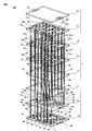
- FIG. 1 is a perspective view showing a multilayer LC filter 100 according to an embodiment.
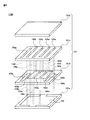
- 2 is an exploded perspective view showing a multilayer LC filter 100.
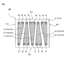
- FIG. 3 is an exploded partial plan view showing a multilayer LC filter 100.
- FIG. 3 is an equivalent circuit diagram of the multilayer LC filter 100.
- FIG. 10 is an exploded perspective view showing a multilayer LC filter 1100 disclosed in Patent Document 1.
- the embodiment is an example of the embodiment of the present invention, and the present invention is not limited to the content of the embodiment.
- the drawings are intended to aid understanding of the specification and may be drawn schematically, and the drawn components and the ratio of dimensions between the components are those described in the specification. May not match the ratio of dimensions.
- the constituent elements described in the specification may be omitted in the drawings or may be drawn with the number omitted.
- FIG. 1 to 4 show a laminated LC filter 100 according to an embodiment.
- 1 is a perspective view
- FIG. 2 is an exploded perspective view
- FIG. 3 is an exploded partial plan view
- FIG. 4 is an equivalent circuit diagram.
- the multilayer LC filter 100 includes a multilayer body 1.
- the input / output terminal 2a and the input / output terminal 2b are formed on the opposite side surfaces (end faces) of the laminate 1.
- Each of the input / output terminal 2 a and the input / output terminal 2 b has one end extending to the lower main surface of the laminate 1 and the other end extending to the upper main surface of the laminate 1.
- a ground terminal 3 is formed on the lower main surface of the laminate 1.
- the laminated body 1 is formed by laminating, for example, eight dielectric layers 1a to 1h made of ceramic or the like in order from the bottom.
- the multilayer body 1 includes a first side E11, a second side E12, and a third side that are connected in order when viewed in the stacking direction of the dielectric layers 1a to 1h. E13 and a fourth side E14 are provided.
- the dielectric layers 1a to 1h constituting the multilayer body 1 will be described.
- An input / output terminal 2a and an input / output terminal 2b are formed on opposite side surfaces (end faces) of the dielectric layer 1a.
- the input / output terminals 2a and 2b are formed on the opposite side surfaces. However, the description thereof may be omitted if not particularly necessary.
- a ground terminal 3 is formed on the lower main surface of the dielectric layer 1a.
- a ground conductor pattern 4 is formed on the upper main surface of the dielectric layer 1a.
- the ground conductor pattern 4 is connected to the ground terminal 3 by via conductors 5a to 5e.
- via conductors 5f to 5l are formed through the upper and lower main surfaces of the dielectric layer 1b.
- FIG. 2 which is an exploded perspective view, the via conductors 5f to 5j are drawn extending downward from the actual direction so that the connection relationship can be understood (the same applies to the via conductors described below). .
- the via conductors 5f to 5l are connected to the ground conductor pattern 4, respectively.
- the capacitor conductor pattern 6a is connected to the input / output terminal 2a.
- the capacitor conductor pattern 6e is connected to the input / output terminal 2b.
- via conductors 5f to 5l are formed through the upper and lower main surfaces of the dielectric layer 1c.
- the via conductors 5f to 5l are also formed in the dielectric layer 1b as described above, but the via conductors having the same reference numerals formed in different dielectric layers mean that both are connected. .
- another eight via conductors 5m to 5t are formed through the upper and lower main surfaces of the dielectric layer 1c.
- the via conductors 5m and 5n are connected to the capacitor conductor pattern 6a, respectively.
- the via conductor 5o is connected to the capacitor conductor pattern 6b.
- the via conductors 5p and 5q are each connected to the capacitor conductor pattern 6c.
- the via conductor 5r is connected to the capacitor conductor pattern 6d.
- the via conductors 5s and 5t are connected to the capacitor conductor pattern 6e, respectively.
- Two capacitor conductor patterns 6f and 6g are formed on the upper main surface of the dielectric layer 1c.
- the capacitor conductor pattern 6f is connected to the via conductors 5m and 5n.
- the capacitor conductor pattern 6g is connected to the via conductors 5s and 5t.
- Two capacitor conductor patterns 6h and 6i are formed on the upper main surface of the dielectric layer 1d.
- the capacitor conductor pattern 6h and the capacitor conductor pattern 6i are connected to each other.
- FIG. 3 shows the upper main surface of the dielectric layer 1e.
- the line-shaped conductor patterns 17a to 17e are arranged so as to extend in the same direction as the first side E11 and the third side E13 facing each other.
- the line-shaped conductor patterns 17a to 17e are formed so that the long sides facing each other are not parallel to each other.
- all of the line-shaped conductor patterns 17a to 17e have sides that are not parallel to any of the first side E11, the second side E12, the third side E13, and the fourth side E14 of the multilayer body 1. Contains at least one.
- One via conductor 5f is connected to the end on the second side E12 side of the line-shaped conductor pattern 17a, and two via conductors 5m, 5n are connected to the end on the fourth side E14 side of the line-shaped conductor pattern 17a. Is connected.
- Two via conductors 5g and 5h are connected to the end on the second side E12 side of the line-shaped conductor pattern 17b, and one via conductor 5o is connected to the end on the fourth side E14 side of the line-shaped conductor pattern 17b. Is connected.
- One via conductor 5i is connected to the end of the line-shaped conductor pattern 17c on the second side E12 side, and two via conductors 5p, 5q are connected to the end of the line-shaped conductor pattern 17c on the fourth side E14 side. Is connected.
- Two via conductors 5j and 5k are connected to the end on the second side E12 side of the line-shaped conductor pattern 17d, and one via conductor 5r is connected to the end on the fourth side E14 side of the line-shaped conductor pattern 17d. Is connected.
- One via conductor 5l is connected to the end of the line-shaped conductor pattern 17e on the second side E12 side, and two via conductors 5s, 5t are connected to the end of the line-shaped conductor pattern 17e on the fourth side E14 side. Is connected.
- the line-shaped conductor patterns 17a to 17e are repeatedly increased and decreased by one, two, one, two, and one at the end on the second side E12 side, for a total of seven vias.
- Conductors 5f to 5l are connected, and a total of eight via conductors 5m to 5t are connected to the end on the fourth side E14 side by repeating increase / decrease with 2, 1, 2, 1, 2 Has been. That is, the multilayer LC filter 100 uses as much space as possible and connects as many via conductors 5f to 5t as possible to the line-shaped conductor patterns 17a to 17e to reduce the internal resistance. I am doing so.
- Line-shaped conductor patterns 27a to 27e are formed on the upper main surface of the dielectric layer 1f. As shown in FIG. 3, the line-shaped conductor patterns 27a to 27e have the same shape as the line-shaped conductor patterns 17a to 17e formed on the upper main surface of the dielectric layer 1e, respectively.
- the via conductors 5f to 5t are connected to the line conductor patterns 27a to 27e at the same positions as the line conductor patterns 17a to 17e.
- Line-shaped conductor patterns 37a to 37e are formed on the upper main surface of the dielectric layer 1g. As shown in FIG. 3, the line-shaped conductor patterns 37a to 37e have the same shape as the line-shaped conductor patterns 17a to 17e formed on the upper main surface of the dielectric layer 1e, respectively. Further, via conductors 5f to 5t are connected to the line conductor patterns 37a to 37e at the same positions as the line conductor patterns 17a to 17e.
- the dielectric layer 1h is a protective layer.
- An input / output terminal 2a and an input / output terminal 2b are formed on opposing side surfaces (end faces) of the dielectric layer 1h.
- the multilayer LC filter 100 having the above structure can be manufactured using materials and manufacturing methods that have been widely used in multilayer LC filters.
- the laminated LC filter 100 includes an equivalent circuit shown in FIG.
- the multilayer LC filter 100 includes a first LC parallel resonator LC1 in which a first inductor L1 and a first capacitor C1 are connected in parallel between an input / output terminal 2a and an input / output terminal 2b.
- a second LC parallel resonator LC2 in which the second inductor L2 and the second capacitor C2 are connected in parallel, and a third LC parallel in which the third inductor L3 and the third capacitor C3 are connected in parallel.
- the fifth LC parallel resonator LC5 is arranged in order.
- the inductor L1 and the inductor L2, the inductor L2 and the inductor L3, the inductor L3 and the inductor L4, and the inductor L4 and the inductor L5 are electromagnetically coupled, respectively.
- the first LC parallel resonator LC1 and the second LC parallel resonator LC2 are capacitively coupled by the capacitor C12.
- the fourth LC parallel resonator LC4 and the fifth LC parallel resonator LC5 are capacitively coupled by a capacitor C45.
- the first LC parallel resonator LC1 and the fifth LC parallel resonator LC5 are capacitively coupled by a capacitor C15.
- the multilayer LC filter 100 composed of the above-described equivalent circuit includes five LC parallel resonators formed between the input / output terminal 2a and the input / output terminal 2b, and constitutes a bandpass filter having a desired frequency characteristic. Yes.
- one via conductor 5f is connected to the end on the second side E12 side of the line-shaped conductor patterns 17a, 27a, 37a, and two via conductors 5m, 5n are connected to the end on the fourth side E14 side.
- the first capacitor C1 is constituted by the capacitance formed between the capacitor conductor pattern 6a and the ground conductor pattern 4.
- the capacitor conductor pattern 6a is connected to the input / output terminal 2a as described above. Then, by connecting the via conductor 5f to the ground conductor pattern 4, the first inductor L1 and the first capacitor C1 are connected in parallel to form the first LC parallel resonator LC1.
- the line-shaped conductor pattern of the first inductor L1 is composed of three layers of line-shaped conductor patterns 17a, 27b, and 37c.
- the internal resistance of the line-shaped conductor pattern is reduced by configuring the number of layers as a plurality of layers.
- the fact that the line-shaped conductor pattern of the first inductor L1 is composed of three layers of line-shaped conductor patterns 17a, 17b, and 17c and the internal resistance is reduced contributes to increasing the Q value of the inductor L1.
- the line-shaped conductor patterns of second to fifth inductors L2 to L5 described later are constituted by a plurality of layers of line-shaped conductor patterns for the same reason.
- Two via conductors 5g and 5h are connected to the end on the second side E12 side of the line-shaped conductor patterns 17b, 27b, and 37b, and one via conductor 5o is connected to the end on the fourth side E14 side.
- a loop-shaped second inductor L2 is configured.
- the second capacitor C2 is configured by the capacitance formed between the capacitor conductor pattern 6b and the ground conductor pattern 4.
- the via conductors 5g and 5h are connected to the ground conductor pattern 4, whereby the second inductor L2 and the second capacitor C2 are connected in parallel, and the second LC parallel resonator LC2 is configured. Yes.
- One via conductor 5i is connected to the end on the second side E12 side of the line-shaped conductor patterns 17c, 27c, and 37c, and two via conductors 5p and 5q are connected to the end on the fourth side E14 side.
- a loop-shaped third inductor L3 is configured.
- the third capacitor C3 is configured by the capacitance formed between the capacitor conductor pattern 6c and the ground conductor pattern 4.
- the via conductor 5i is connected to the ground conductor pattern 4, whereby the third inductor L3 and the third capacitor C3 are connected in parallel to form a third LC parallel resonator LC3.
- the fourth capacitor C4 is configured by the capacitance formed between the capacitor conductor pattern 6d and the ground conductor pattern 4.
- the via conductors 5j and 5k are connected to the ground conductor pattern 4, whereby the fourth inductor L4 and the fourth capacitor C4 are connected in parallel, and the fourth LC parallel resonator LC4 is configured. Yes.
- One via conductor 5l is connected to the end on the second side E12 side of the line-shaped conductor patterns 17e, 27e, 37e, and two via conductors 5s, 5t are connected to the end on the fourth side E14 side.
- a loop-shaped fifth inductor L5 is configured.
- the fifth capacitor C5 is configured by the capacitance formed between the capacitor conductor pattern 6d and the ground conductor pattern 4.
- the capacitor conductor pattern 6d is connected to the input / output terminal 2b as described above. Then, by connecting the via conductor 5l to the ground conductor pattern 4, the fifth inductor L5 and the fifth capacitor C5 are connected in parallel to form a fifth LC parallel resonator LC5.
- the capacitor C12 is constituted by the capacitance formed between the capacitor conductor pattern 6f and the capacitor conductor pattern 6b. As described above, the capacitor conductor pattern 6f is connected to the via conductors 5m and 5n. The capacitor conductor pattern 6b is also a conductor pattern of the second capacitor C2.
- the capacitor C45 is configured by the capacitance formed between the capacitor conductor pattern 6g and the capacitor conductor pattern 6d. As described above, the capacitor conductor pattern 6g is connected to the via conductors 5s and 5t. The capacitor conductor pattern 6d is also a conductor pattern of the fourth capacitor C4.
- the capacitor C15 is configured by the capacitance formed between the capacitor conductor pattern 6f and the capacitor conductor pattern 6h and the capacitance formed between the capacitor conductor pattern 6g and the capacitor conductor pattern 6i. As described above, the capacitor conductor pattern 6f is connected to the via conductors 5m and 5n, the capacitor conductor pattern 6h and the capacitor conductor pattern 6i are connected to each other, and the capacitor conductor pattern 6g is connected to the via conductors 5s and 5t.
- the multilayer LC filter 100 includes the equivalent circuit shown in FIG. 4 inside the multilayer body 1.
- one via conductor 5f is connected to the second side E12 side with respect to the line-shaped conductor patterns 17a, 27a, and 37a of the first inductor L1.
- two via conductors 5m and 5n are connected to the fourth side E14 side, and conversely to the line-shaped conductor patterns 17b, 27b, and 37b of the second inductor L2, the second side E12 side
- Two via conductors 5g and 5f are connected to each other, one via conductor 5o is connected to the fourth side E14 side, and the same relationship is applied to the third to fifth inductors L3 to L5.
- the limited space in the multilayer body 1 is effectively utilized, the increase in the number of via conductors is suppressed while suppressing the increase in size, and the internal resistances of the inductors L1 to L5 are reduced, respectively.
- Increase the Q value of Te is made smaller input-output terminal 2a, an insertion loss between 2b efficiently.
- the line-shaped conductor patterns 17a to 17e, 27a to 27e, and 37a to 37e are formed so that the long sides facing each other are not parallel to each other, and in a limited space, The area of these line conductor patterns is increased as much as possible.
- the line-shaped conductor patterns 17a to 17e, 27a to 27e, and 37a to 37e are formed so that the long sides facing each other are not parallel to each other. This contributes to increasing the Q value of the inductors L1 to L5.
- the multilayer LC filter 100 has the inductors L1 to L5 of the LC parallel resonators LC1 to LC5 when the side surface of the multilayer body 1 is seen through from the first side E11 side to the third side E13 side.
- the winding direction is all the same.
- electromagnetic coupling between inductors of adjacent LC parallel resonators is strengthened, and the frequency characteristics are widened. If it is desired to form a band narrower than the frequency characteristics of the multilayer LC filter 100, the winding direction of some of the inductors L1 to L5 may be reversed.
- the multilayer LC filter 100 according to the embodiment has been described above.
- the present invention is not limited to the contents described above, and various modifications can be made in accordance with the spirit of the invention.
- the multilayer LC filter 100 is a five-stage bandpass filter including five LC parallel resonators LC1 to LC5.
- the multilayer LC filter of the present invention is not limited to a bandpass filter, and is a high-pass filter. Other types of filters such as filters and low-pass filters may be used.
- the LC resonator formed in the multilayer LC filter of the present invention is not limited to the LC parallel resonator, and may be an LC series resonator.
- the number of stages of the multilayer LC filter of the present invention is not limited to five, and may be smaller or larger.
- One via conductor 5f to 5l is connected, and two, one, two, one, and two via conductors 5m to 5t are connected at the end on the fourth side E14 side.
- These numbers can be changed in accordance with the provisions of the present invention.
- two, three, two, three and two via conductors are connected at the end on the second side E12 side, and three and two are connected at the end on the fourth side E14 side.
- Three, two, and three via conductors may be connected.
- one, three, one, three, and one via conductor are connected at the end on the second side E12 side, and three, one at the end on the fourth side E14 side.
- Three, one, and three via conductors may be connected.
- the multilayer LC filter 100 uses a characteristic method of connecting via conductors to the line-shaped conductor pattern of the present invention in all LC resonators (LC parallel resonators LC1 to LC5) formed in the multilayer body 1.
- the via conductor connection method for the characteristic line-shaped conductor pattern of the present invention may be employed.
- the insertion loss of the multilayer LC filter is more effectively suppressed while suppressing the increase in size when the via conductor connection method to the characteristic line-shaped conductor pattern of the present invention is adopted. Can be reduced.
Landscapes
- Engineering & Computer Science (AREA)
- Power Engineering (AREA)
- Microelectronics & Electronic Packaging (AREA)
- Manufacturing & Machinery (AREA)
- Filters And Equalizers (AREA)
- Coils Or Transformers For Communication (AREA)
Abstract
LC共振器を構成するインダクタのQ値が大きく、挿入損失が改善された積層型LCフィルタを提供する。 第1のインダクタL1の線路状導体パターン17a、27a、37aに対しては、第2の辺E12側に1本のビア導体5fを接続し、第4の辺E14側に2本のビア導体5m、5nを接続し、第2のインダクタL2の線路状導体パターン17b、27b、37bに対しては、逆に、第2の辺E12側に2本のビア導体5g、5fを接続し、第4の辺E14側に1本のビア導体5oを接続し、以下、第3~第5のインダクタL3~L5に対しても、同様の関係を繰り返す。
Description
本発明は、積層体の内部に複数のLC共振器を備えた積層型LCフィルタに関し、さらに詳しくは、LC共振器を構成するインダクタのQ値が大きく、挿入損失が改善された積層型LCフィルタに関する。
複数の誘電体層が積層された積層体の内部に、インダクタとキャパシタとからなるLC共振器が形成された積層型LCフィルタが、種々の電子機器に使用されている。
そのような積層型LCフィルタが、特許文献1(WO2007/119356号公報)に開示されている。
図5に、特許文献1に開示された積層型LCフィルタ(積層帯域通過フィルタ)1100を示す。
積層型LCフィルタ1100は、グランド導体パターン形成層(接地電極形成層)101a、キャパシタ導体パターン形成層(キャパシタ電極形成層)101b、線路状導体パターン形成層(線路電極形成層)101c、外層101dからなる、複数の誘電体層が積層された積層体101を備える。
グランド導体パターン形成層101aの上側主面には、グランド導体パターン(接地導体パターン)102が形成されている。グランド導体パターン102は、積層体101の対向する2つの側面に形成されたグランド端子(接地端子;図示せず)に、それぞれ引き出されている。
キャパシタ導体パターン形成層101bの上側主面には、5つのキャパシタ導体パターン103a~103eが形成されている。そのうち、キャパシタ導体パターン103a、103eは、グランド端子が形成されていない別の側面にそれぞれ形成された入出力端子(図示せず)に、それぞれ引き出されている。
また、キャパシタ導体パターン形成層101bには、5つのビア導体(ビア電極)104a~104eが形成されている。
線路状導体パターン形成層101cの上側主面には、5つの線路状導体パターン105a~105eが形成されている。
また、線路状導体パターン形成層101cにも、前出の5つのビア導体104a~104eが形成されている。さらに、線路状導体パターン形成層101cには、別の5つのビア導体104f~104jが形成されている。
外層101dは、保護層であり、導体パターン、ビア導体は形成されていない。
ビア導体104f、線路状導体パターン105a、ビア導体104aが接続されて、キャパシタ導体パターン103aとグランド導体パターン102との間に、ループ状の第1のインダクタが構成されている。また、キャパシタ導体パターン103aとグランド導体パターン102とで第1のキャパシタが構成されている。そして、第1のインダクタと第1のキャパシタとが並列に接続されて、第1のLC並列共振器が構成されている。
ビア導体104g、線路状導体パターン105b、ビア導体104bが接続されて、キャパシタ導体パターン103bとグランド導体パターン102との間に、ループ状の第2のインダクタが構成されている。また、キャパシタ導体パターン103bとグランド導体パターン102とで第2のキャパシタが構成されている。そして、第2のインダクタと第2のキャパシタとが並列に接続されて、第2のLC並列共振器が構成されている。
ビア導体104h、線路状導体パターン105c、ビア導体104cが接続されて、キャパシタ導体パターン103cとグランド導体パターン102との間に、ループ状の第3のインダクタが構成されている。また、キャパシタ導体パターン103cとグランド導体パターン102とで第3のキャパシタが構成されている。そして、第3のインダクタと第3のキャパシタとが並列に接続されて、第3のLC並列共振器が構成されている。
ビア導体104i、線路状導体パターン105d、ビア導体104dが接続されて、キャパシタ導体パターン103dとグランド導体パターン102との間に、ループ状の第4のインダクタが構成されている。また、キャパシタ導体パターン103dとグランド導体パターン102とで第4のキャパシタが構成されている。そして、第4のインダクタと第4のキャパシタとが並列に接続されて、第4のLC並列共振器が構成されている。
ビア導体104j、線路状導体パターン105e、ビア導体104eが接続されて、キャパシタ導体パターン103eとグランド導体パターン102との間に、ループ状の第5のインダクタが構成されている。また、キャパシタ導体パターン103eとグランド導体パターン102とで第5のキャパシタが構成されている。そして、第5のインダクタと第5のキャパシタとが並列に接続されて、第5のLC並列共振器が構成されている。
積層型LCフィルタ1100は、上述したように、積層体101の内部に、第1~第5の5つのLC並列共振器が形成されている。そして、積層型LCフィルタ1100は、一方の入出力端子が第1のLC並列共振器に接続され、他方の入出力端子が第5のLC並列共振器に接続され、さらに、隣接するLC並列共振器のインダクタどうしが電磁界結合されて、5段のLCバンドパスフィルタが構成されている。
このように、積層型LCフィルタ1100は、複数のLC並列共振器のインダクタが、それぞれビア導体と線路状導体パターンとでループを形成したものからなり、かつ、LC並列共振器が配列された方向に見た場合に、互いに結合するLC並列共振器のインダクタのループ面どうしが少なくとも一部で重なっているため、両者の結合度は高められており、フィルタ特性の広帯域化がはかられている。
積層型LCフィルタを含め、電子部品は、電子機器の消費電力を抑制することができるため、可能な限り挿入損失が小さいことが望ましい。特に、移動体通信機器など、バッテリーにより駆動される電子機器に使用される電子部品に対しては、挿入損失が小さいことが強く求められている。
しかしながら、特許文献1に開示された積層型LCフィルタ1100は、各LC共振器のインダクタが、直方体形状の積層体の一方の長辺側側面の付近に設けられたビア導体と、他方の長辺側側面の付近に設けられたビア導体と、両ビア導体のビア径とほぼ同じ幅の線路状導体パターンとからなる、平均断面積の小さい単純な構成であるため、比較的、内部抵抗値が大きく、Q値が不十分で、求められる小さな挿入損失を得られないおそれがあった。
本発明は上記のような課題を解決するためになされたものであり、その目的は、特許文献1のようなビア導体を使ったループ状のインダクタを有するLC共振器を含む積層型LCフィルタにおいて、LC共振器のQ値を向上させ、挿入損失を小さくすることである。
本発明は、上述した従来の課題を解決するためになされたものであり、その手段として本発明の積層型LCフィルタは、複数の誘電体層が積層された直方体状の積層体と、誘電体層の層間に形成された複数の線路状導体パターンと、誘電体層の層間に形成された複数のキャパシタ導体パターンと、誘電体層の層間に形成された少なくとも1つのグランド導体パターンと、誘電体層を貫通して形成された複数のビア導体と、を備え、線路状導体パターンの両端にビア導体が接続されることにより、複数のループ状のインダクタが形成され、キャパシタ導体パターンとグランド導体パターンの間に形成される容量により、または、1対のキャパシタ導体パターンの間に形成される容量により、複数のキャパシタが形成され、インダクタとキャパシタとが接続されることにより、少なくとも2つのLC共振器が形成され、積層体は、誘電体層の積層方向に見た場合に、順に繋がった、第1の辺、第2の辺、第3の辺、第4の辺を備え、積層体を、誘電体層の積層方向に透視した場合に、複数のLC共振器の線路状導体パターンには、それぞれ、積層体の第2の辺側および第4の辺側において、ビア導体が接続され、少なくとも1つの線路状導体パターンは、第2の辺側と第4の辺側とにおいて、異なる本数のビア導体が接続されたものとした。
順に並んだLC共振器の中から、第1から第Nまで連続して並んだ任意の2つ以上のLC共振器を見た場合に、第1および第2のLC共振器のうち、一方のLC共振器の線路状導体パターンには、第4の辺側において、第2の辺側よりも多くの本数のビア導体が接続され、他方のLC共振器の線路状導体パターンには、第2の辺側において、第4の辺側よりも多くの本数のビア導体が接続され、第3以降の第NのLC共振器は、奇数番のLC共振器の線路状導体パターンには、第1のLC共振器と同じ条件でビア導体が接続され、偶数番のLC共振器の線路状導体パターンには、第2のLC共振器と同じ条件でビア導体が接続されたものであることが好ましい。ただし、Nは2以上の整数である。この場合には、大型化を抑制しながら、ビア導体の本数を増やして内部抵抗を小さくし、インダクタのQ値を大きくして、積層型LCフィルタの挿入損失を小さくしすることができる。
積層型LCフィルタは、積層体内にN個のLC共振器が形成され、第1から第Nまで連続して並んだ全てのLC共振器を見た場合に、第1および第2のLC共振器のうち、一方のLC共振器の線路状導体パターンには、第4の辺側において、第2の辺側よりも多くの本数のビア導体が接続され、他方のLC共振器の線路状導体パターンには、第2の辺側において、第4の辺側よりも多くの本数のビア導体が接続され、第3以降の第NのLC共振器は、奇数番のLC共振器の線路状導体パターンには、第1のLC共振器と同じ条件でビア導体が接続され、偶数番のLC共振器の線路状導体パターンには、第2のLC共振器と同じ条件でビア導体が接続されることがさらに好ましい。このように、内部に形成された全てのLC共振器において、本発明の特徴的な線路状導体パターンへのビア導体の接続方法を適用した場合には、より効果的に、大型化を抑制しながら、ビア導体の本数を増やして内部抵抗を小さくし、インダクタのQ値を大きくして、積層型LCフィルタの挿入損失を小さくすることができる。
積層型LCフィルタは、第1および第2のLC共振器のうち、一方のLC共振器の線路状導体パターンには、第2の辺側において1本のビア導体が接続され、第4の辺側において2本のビア導体が接続され、他方のLC共振器の線路状導体パターンには、第2の辺側において2本のビア導体が接続され、第4の辺側において1本のビア導体が接続されたものとすることが好ましい。この場合にも、より効果的に、大型化を抑制しながら、ビア導体の本数を増やして内部抵抗を小さくし、インダクタのQ値を大きくして、積層型LCフィルタの挿入損失を小さくすることができる。
積層型LCフィルタは、第1および第2のLC共振器の線路状導体パターンが、いずれも積層体の第1の辺ないし第4の辺に非平行な辺を含むことが好ましい。この場合にも、より効果的に、大型化を抑制しながら、線路状導体パターンの内部抵抗を小さくし、インダクタのQ値を大きくして、積層型LCフィルタの挿入損失を小さくすることができる。
また、積層型LCフィルタは、隣接するLC共振器のインダクタどうしが電磁界結合され、積層体の側面を、第1の辺側から第3の辺側に向かって透視した場合に、全てのLC共振器のインダクタの巻回方向が同一であることが好ましい。この場合には、隣接するLC共振器のインダクタどうしの電磁界結合を強めることができ、より広帯域化した周波数特性を備えた積層型LCフィルタを得ることができる。
あるいは、積層型LCフィルタは、隣接するLC共振器のインダクタどうしが電磁界結合され、積層体の側面を、第1の辺側から第3の辺側に向かって透視した場合に、一部のLC共振器のインダクタの巻回方向と、残りのLC共振器のインダクタの巻回方向とが異なることも好ましい。この場合には、一部の隣接するLC共振器のインダクタどうしの電磁界結合を弱めることができ、所望の周波数特性を備えた積層型LCフィルタを得ることができる。
本発明の積層型LCフィルタは、可能な限り大型化を抑制したうえで、LC共振器のインダクタの内部抵抗が小さくされ、インダクタのQ値が大きくされ、挿入損失が小さくされている。
以下、図面とともに、本発明を実施するための形態について説明する。
なお、実施形態は、本発明の実施の形態を例示的に示したものであり、本発明が実施形態の内容に限定されることはない。また、図面は、明細書の理解を助けるためのものであり、模式的に描画されている場合があり、描画された構成要素および構成要素間の寸法の比率が、明細書に記載されたそれらの寸法の比率と一致していない場合がある。また、明細書に記載されている構成要素が、図面において省略されている場合や、個数を省略して描画されている場合などがある。
図1~図4に、実施形態にかかる積層型LCフィルタ100を示す。ただし、図1は斜視図、図2は分解斜視図、図3は分解部分平面図、図4は等価回路図である。
積層型LCフィルタ100は、積層体1を備える。
積層体1の対向する側面(端面)に、入出力端子2aと入出力端子2bとが形成されている。入出力端子2aと入出力端子2bとは、それぞれ、一端が積層体1の下側主面に延出し、他端が積層体1の上側主面に延出している。また、積層体1の下側主面に、グランド端子3が形成されている。
積層体1は、図2に示すように、たとえばセラミックなどからなる8層の誘電体層1a~1hが下から順に積層されたものからなる。
積層体1は、図1および図3に示すように、誘電体層1a~1hの積層方向に見た場合に、順に繋がった、第1の辺E11、第2の辺E12、第3の辺E13、第4の辺E14を備えている。
以下において、まず、積層体1を構成する各誘電体層1a~1hについて説明する。
誘電体層1aの対向する側面(端面)に、入出力端子2aと入出力端子2bとが形成されている。なお、以下に説明する誘電体層1b~1hにおいても、対向する側面に入出力端子2a、2bが形成されているが、特に必要がない場合には、その説明を省略する場合がある。
誘電体層1aの下側主面に、グランド端子3が形成されている。
誘電体層1aの上下主面間を貫通して、5つのビア導体5a~5eが形成されている。
誘電体層1aの上側主面に、グランド導体パターン4が形成されている。グランド導体パターン4は、ビア導体5a~5eによって、グランド端子3に接続されている。
誘電体層1bの上下主面間を貫通して、7本のビア導体5f~5lが形成されている。なお、分解斜視図である図2においては、接続関係が分かるように、ビア導体5f~5jを、それぞれ、実際よりも下方向に伸ばして描写している(以下に説明するビア導体において同じ)。ビア導体5f~5lは、それぞれ、グランド導体パターン4に接続されている。
誘電体層1bの上側主面に、5つのキャパシタ導体パターン6a~6eが形成されている。キャパシタ導体パターン6aは入出力端子2aに接続されている。キャパシタ導体パターン6eは入出力端子2bに接続されている。
誘電体層1cの上下主面間を貫通して、7本のビア導体5f~5lが形成されている。なお、ビア導体5f~5lは、上述したように誘電体層1bにも形成されているが、異なる誘電体層に形成された同じ符号のビア導体は、両者が接続されていることを意味する。また、誘電体層1cの上下主面間を貫通して、別の8本のビア導体5m~5tが形成されている。ビア導体5m、5nは、それぞれ、キャパシタ導体パターン6aに接続されている。ビア導体5oは、キャパシタ導体パターン6bに接続されている。ビア導体5p、5qは、それぞれ、キャパシタ導体パターン6cに接続されている。ビア導体5rは、キャパシタ導体パターン6dに接続されている。ビア導体5s、5tは、それぞれ、キャパシタ導体パターン6eに接続されている。
誘電体層1cの上側主面に、2つのキャパシタ導体パターン6f、6gが形成されている。キャパシタ導体パターン6fは、ビア導体5m、5nに接続されている。また、キャパシタ導体パターン6gは、ビア導体5s、5tに接続されている。
誘電体層1dの上下主面間を貫通して、7本のビア導体5f~5lと、8本のビア導体5m~5tとが形成されている。
誘電体層1dの上側主面に、2つのキャパシタ導体パターン6h、6iが形成されている。キャパシタ導体パターン6hとキャパシタ導体パターン6iとは、相互に接続されている。
誘電体層1eの上下主面間を貫通して、7本のビア導体5f~5lと、8本のビア導体5m~5tとが形成されている。
誘電体層1eの上側主面に、5つの線路状導体パターン17a~17eが形成されている。図3に、誘電体層1eの上側主面を示す。線路状導体パターン17a~17eは、それぞれ、対向する第1の辺E11および第3の辺E13と同じ方向に延びるように配置されている。線路状導体パターン17a~17eは、それぞれ、対向する長辺が相互に非平行となるように形成されている。その結果、線路状導体パターン17a~17eは、いずれも、積層体1の第1の辺E11、第2の辺E12、第3の辺E13、第4の辺E14のいずれとも平行でない辺を、少なくとも1つ含んでいる。
線路状導体パターン17aの第2の辺E12側の端部に1本のビア導体5fが接続され、線路状導体パターン17aの第4の辺E14側の端部に2本のビア導体5m、5nが接続されている。線路状導体パターン17bの第2の辺E12側の端部に2本のビア導体5g、5hが接続され、線路状導体パターン17bの第4の辺E14側の端部に1本のビア導体5oが接続されている。線路状導体パターン17cの第2の辺E12側の端部に1本のビア導体5iが接続され、線路状導体パターン17cの第4の辺E14側の端部に2本のビア導体5p、5qが接続されている。線路状導体パターン17dの第2の辺E12側の端部に2本のビア導体5j、5kが接続され、線路状導体パターン17dの第4の辺E14側の端部に1本のビア導体5rが接続されている。線路状導体パターン17eの第2の辺E12側の端部に1本のビア導体5lが接続され、線路状導体パターン17eの第4の辺E14側の端部に2本のビア導体5s、5tが接続されている。
以上のように、線路状導体パターン17a~17eは、第2の辺E12側の端部に、1本、2本、1本、2本、1本と増減を繰り返して、合計7本のビア導体5f~5lが接続され、第4の辺E14側の端部に、2本、1本、2本、1本、2本と増減を繰り返して、合計8本のビア導体5m~5tが接続されている。すなわち、積層型LCフィルタ100は、スペースを可能な限り有効に利用したうえで、線路状導体パターン17a~17eに、可能な限り多い本数のビア導体5f~5tを接続し、内部抵抗を小さくするようにしている。
誘電体層1fの上下主面間を貫通して、7本のビア導体5f~5lと、8本のビア導体5m~5tとが形成されている。
誘電体層1fの上側主面に、5つの線路状導体パターン27a~27eが形成されている。線路状導体パターン27a~27eは、図3に示すように、誘電体層1eの上側主面に形成された線路状導体パターン17a~17eと、それぞれ、同じ形状からなる。また、線路状導体パターン27a~27eには、線路状導体パターン17a~17eと同じ位置において、ビア導体5f~5tが接続されている。
誘電体層1gの上下主面間を貫通して、7本のビア導体5f~5lと、8本のビア導体5m~5tとが形成されている。
誘電体層1gの上側主面に、5つの線路状導体パターン37a~37eが形成されている。線路状導体パターン37a~37eは、図3に示すように、誘電体層1eの上側主面に形成された線路状導体パターン17a~17eと、それぞれ、同じ形状からなる。また、線路状導体パターン37a~37eには、線路状導体パターン17a~17eと同じ位置において、ビア導体5f~5tが接続されている。
誘電体層1hは、保護層である。誘電体層1hの対向する側面(端面)に、入出力端子2aと入出力端子2bとが形成されている。
以上の構造からなる積層型LCフィルタ100は、従来から積層型LCフィルタにおいて広く使用されている材料および製造方法を使用して、製造することができる。
積層型LCフィルタ100は、図4に示す等価回路を備えている。
積層型LCフィルタ100は、入出力端子2aと入出力端子2bとの間に、第1のインダクタL1と第1のキャパシタC1とが並列に接続された第1のLC並列共振器LC1と、第2のインダクタL2と第2のキャパシタC2とが並列に接続された第2のLC並列共振器LC2と、第3のインダクタL3と第3のキャパシタC3とが並列に接続された第3のLC並列共振器LC3と、第4のインダクタL4と第4のキャパシタC4とが並列に接続された第4のLC並列共振器LC4と、第5のインダクタL5と第5のキャパシタC5とが並列に接続された第5のLC並列共振器LC5とが、順に配置されている。そして、インダクタL1とインダクタL2とが、インダクタL2とインダクタL3とが、インダクタL3とインダクタL4とが、インダクタL4とインダクタL5とが、それぞれ、電磁界結合されている。また、第1のLC並列共振器LC1と第2のLC並列共振器LC2とが、キャパシタC12によって、容量結合されている。第4のLC並列共振器LC4と第5のLC並列共振器LC5とが、キャパシタC45によって、容量結合されている。第1のLC並列共振器LC1と第5のLC並列共振器LC5とが、キャパシタC15によって、容量結合されている。
以上の等価回路からなる積層型LCフィルタ100は、入出力端子2aと入出力端子2bとの間に5つのLC並列共振器が形成され、所望の周波数特性を備えたバンドパスフィルタを構成している。
次に、積層型LCフィルタ100の構造と等価回路との関係について説明する。
まず、線路状導体パターン17a、27a、37aの第2の辺E12側の端部に1本のビア導体5fが接続され、第4の辺E14側の端部に2本のビア導体5m、5nが接続されて、ループ状の第1のインダクタL1が構成されている。また、キャパシタ導体パターン6aとグランド導体パターン4との間に形成される容量により、第1のキャパシタC1が構成されている。なお、キャパシタ導体パターン6aは、上述したとおり、入出力端子2aに接続されている。そして、ビア導体5fがグランド導体パターン4に接続されることによって、第1のインダクタL1と第1のキャパシタC1とが並列に接続されて、第1のLC並列共振器LC1が構成されている。
なお、第1のインダクタL1の線路状導体パターンは、3層の線路状導体パターン17a、27b、37cによって構成されている。これは、層数を複数層で構成することによって、線路状導体パターンの内部抵抗を小さくしたものである。第1のインダクタL1の線路状導体パターンを3層の線路状導体パターン17a、17b、17cで構成し、内部抵抗を小さくしたことは、インダクタL1のQ値を大きくすることに寄与している。なお、後述する第2~第5のインダクタL2~L5の線路状導体パターンが、複数層の線路状導体パターンによって構成されているのも、同じ理由である。
線路状導体パターン17b、27b、37bの第2の辺E12側の端部に2本のビア導体5g、5hが接続され、第4の辺E14側の端部に1本のビア導体5oが接続されて、ループ状の第2のインダクタL2が構成されている。また、キャパシタ導体パターン6bとグランド導体パターン4との間に形成される容量により、第2のキャパシタC2が構成されている。そして、ビア導体5g、5hがグランド導体パターン4に接続されることによって、第2のインダクタL2と第2のキャパシタC2とが並列に接続されて、第2のLC並列共振器LC2が構成されている。
線路状導体パターン17c、27c、37cの第2の辺E12側の端部に1本のビア導体5iが接続され、第4の辺E14側の端部に2本のビア導体5p、5qが接続されて、ループ状の第3のインダクタL3が構成されている。また、キャパシタ導体パターン6cとグランド導体パターン4との間に形成される容量により、第3のキャパシタC3が構成されている。そして、ビア導体5iがグランド導体パターン4に接続されることによって、第3のインダクタL3と第3のキャパシタC3とが並列に接続されて、第3のLC並列共振器LC3が構成されている。
線路状導体パターン17d、27d、37dの第2の辺E12側の端部に2本のビア導体5j、5kが接続され、第4の辺E14側の端部に1本のビア導体5rが接続されて、ループ状の第4のインダクタL4が構成されている。また、キャパシタ導体パターン6dとグランド導体パターン4との間に形成される容量により、第4のキャパシタC4が構成されている。そして、ビア導体5j、5kがグランド導体パターン4に接続されることによって、第4のインダクタL4と第4のキャパシタC4とが並列に接続されて、第4のLC並列共振器LC4が構成されている。
線路状導体パターン17e、27e、37eの第2の辺E12側の端部に1本のビア導体5lが接続され、第4の辺E14側の端部に2本のビア導体5s、5tが接続されて、ループ状の第5のインダクタL5が構成されている。また、キャパシタ導体パターン6dとグランド導体パターン4との間に形成される容量により、第5のキャパシタC5が構成されている。なお、キャパシタ導体パターン6dは、上述したとおり、入出力端子2bに接続されている。そして、ビア導体5lがグランド導体パターン4に接続されることによって、第5のインダクタL5と第5のキャパシタC5とが並列に接続されて、第5のLC並列共振器LC5が構成されている。
また、キャパシタ導体パターン6fとキャパシタ導体パターン6bとの間に形成される容量により、キャパシタC12が構成されている。上述したとおり、キャパシタ導体パターン6fは、ビア導体5m、5nに接続されている。また、キャパシタ導体パターン6bは、第2のキャパシタC2の導体パターンでもある。
キャパシタ導体パターン6gとキャパシタ導体パターン6dとの間に形成される容量により、キャパシタC45が構成されている。上述したとおり、キャパシタ導体パターン6gは、ビア導体5s、5tに接続されている。また、キャパシタ導体パターン6dは、第4のキャパシタC4の導体パターンでもある。
キャパシタ導体パターン6fとキャパシタ導体パターン6hとの間に形成される容量、および、キャパシタ導体パターン6gとキャパシタ導体パターン6iとの間に形成される容量により、キャパシタC15が構成されている。上述したとおり、キャパシタ導体パターン6fがビア導体5m、5nに接続され、キャパシタ導体パターン6hとキャパシタ導体パターン6iとが相互に接続され、キャパシタ導体パターン6gがビア導体5s、5tに接続されている。
以上の関係により、積層型LCフィルタ100は、積層体1の内部に、図4に示す等価回路を備えている。
積層型LCフィルタ100は、図3に示したように、第1のインダクタL1の線路状導体パターン17a、27a、37aに対しては、第2の辺E12側に1本のビア導体5fを接続し、第4の辺E14側に2本のビア導体5m、5nを接続し、第2のインダクタL2の線路状導体パターン17b、27b、37bに対しては、逆に、第2の辺E12側に2本のビア導体5g、5fを接続し、第4の辺E14側に1本のビア導体5oを接続し、以下、第3~第5のインダクタL3~L5に対しても、同様の関係を繰り返すことにより、積層体1内の限られたスペースを有効に活かし、大型化を抑制しながら、ビア導体の本数を増やして、インダクタL1~L5の内部抵抗をそれぞれ小さくし、インダクタL1~L5のQ値をそれぞれ大きくして、入出力端子2a、2b間の挿入損失を効率的に小さくしている。
また、積層型LCフィルタ100は、線路状導体パターン17a~17e、27a~27e、37a~37eを、それぞれ、対向する長辺が相互に非平行となるように形成し、限られたスペースにおいて、これらの線路状導体パターンの面積をそれぞれ可能な限り大きくしている。このように、線路状導体パターン17a~17e、27a~27e、37a~37eを、それぞれ、対向する長辺が相互に非平行となるように形成したことも、線路状導体パターンの内部抵抗を小さくし、インダクタL1~L5のQ値を大きくすることに寄与している。
また、積層型LCフィルタ100は、積層体1の側面を、第1の辺E11側から第3の辺E13側に向かって透視した場合に、LC並列共振器LC1~LC5のインダクタL1~L5の巻回方向が、全て同一になっている。この結果、積層型LCフィルタ100は、隣接するLC並列共振器のインダクタどうしの電磁界結合が強められており、周波数特性が広帯域化されている。なお、積層型LCフィルタ100の周波数特性よりも狭い帯域を形成したい場合には、インダクタL1~L5のうちの、一部のものの巻回方向を、逆方向にすれば良い。
以上、実施形態にかかる積層型LCフィルタ100について説明した。しかしながら、本発明が上述した内容に限定されることはなく、発明の趣旨に沿って、種々の変更をなすことができる。
たとえば、積層型LCフィルタ100は、5つのLC並列共振器LC1~LC5を備えた5段のバンドパスフィルタであったが、本発明の積層型LCフィルタは、バンドパスフィルタには限られず、ハイパスフィルタ、ローパスフィルタなど、他の種類のフィルタであっても良い。また、本発明の積層型LCフィルタの内部に形成されるLC共振器は、LC並列共振器には限られず、LC直列共振器などであっても良い。さらに、本発明の積層型LCフィルタの段数は5段には限られず、それよりも少なくても良く、それよりも多くても良い。
また、積層型LCフィルタ100では、線路状導体パターン17a~17e(27a~27e、37a~37e)に対し、第2の辺E12側の端部において、2本、2本、1本、2本、1本のビア導体5f~5lを接続し、第4の辺E14側の端部において、2本、1本、2本、1本、2本のビア導体5m~5tを接続しているが、これらの本数は、本件発明の規定に沿って変更することができる。たとえば、第2の辺E12側の端部において、2本、3本、2本、3本、2本のビア導体を接続し、第4の辺E14側の端部において、3本、2本、3本、2本、3本のビア導体を接続するようにしても良い。あるいは、第2の辺E12側の端部において、1本、3本、1本、3本、1本のビア導体を接続し、第4の辺E14側の端部において、3本、1本、3本、1本、3本のビア導体を接続するようにしても良い。
また、積層型LCフィルタ100は、積層体1内に形成された全てのLC共振器(LC並列共振器LC1~LC5)において、本発明の特徴的な線路状導体パターンに対するビア導体の接続方法を採用しているが、積層体1内に形成された一部の隣接するLC共振器において、本発明の特徴的な線路状導体パターンに対するビア導体の接続方法を採用しても良い。ただし、全てのLC共振器において、本発明の特徴的な線路状導体パターンに対するビア導体の接続方法を採用した方が、より効率的に、大型化を抑制しながら、積層型LCフィルタの挿入損失を小さくすることができる。
1・・・積層体
1a~1h・・・誘電体層
E11・・・第1の辺
E12・・・第2の辺
E13・・・第3の辺
E14・・・第4の辺
2a、2b・・・入出力端子
3・・・グランド端子
4・・・グランド導体パターン
5a~5t・・・ビア導体
6a~6i・・・キャパシタ導体パターン
17a~17e、27a~27e、37a~37e・・・線路状導体パターン
1a~1h・・・誘電体層
E11・・・第1の辺
E12・・・第2の辺
E13・・・第3の辺
E14・・・第4の辺
2a、2b・・・入出力端子
3・・・グランド端子
4・・・グランド導体パターン
5a~5t・・・ビア導体
6a~6i・・・キャパシタ導体パターン
17a~17e、27a~27e、37a~37e・・・線路状導体パターン
Claims (7)
- 複数の誘電体層が積層された直方体状の積層体と、
前記誘電体層の層間に形成された複数の線路状導体パターンと、
前記誘電体層の層間に形成された複数のキャパシタ導体パターンと、
前記誘電体層の層間に形成された少なくとも1つのグランド導体パターンと、
前記誘電体層を貫通して形成された複数のビア導体と、を備え、
前記線路状導体パターンの両端に前記ビア導体が接続されることにより、複数のループ状のインダクタが形成され、
前記キャパシタ導体パターンと前記グランド導体パターンの間に形成される容量により、または、1対の前記キャパシタ導体パターンの間に形成される容量により、複数のキャパシタが形成され、
前記インダクタと前記キャパシタとが接続されることにより、少なくとも2つのLC共振器が形成された積層型LCフィルタであって、
前記積層体は、前記誘電体層の積層方向に見た場合に、順に繋がった、第1の辺、第2の辺、第3の辺、第4の辺を備え、
前記積層体を、前記誘電体層の積層方向に透視した場合に、
複数の前記LC共振器の前記線路状導体パターンには、それぞれ、前記積層体の前記第2の辺側および前記第4の辺側において、前記ビア導体が接続され、
少なくとも1つの前記線路状導体パターンは、前記第2の辺側と前記第4の辺側とにおいて、異なる本数の前記ビア導体が接続された積層型LCフィルタ。 - 順に並んだ前記LC共振器の中から、第1から第Nまで連続して並んだ任意の2つ以上の前記LC共振器を見た場合に、
第1および第2の前記LC共振器のうち、一方の前記LC共振器の前記線路状導体パターンには、前記第4の辺側において、前記第2の辺側よりも多くの本数の前記ビア導体が接続され、他方の前記LC共振器の前記線路状導体パターンには、前記第2の辺側において、前記第4の辺側よりも多くの本数の前記ビア導体が接続され、
第3以降の第Nの前記LC共振器は、奇数番の前記LC共振器の前記線路状導体パターンには、第1の前記LC共振器と同じ条件で前記ビア導体が接続され、偶数番の前記LC共振器の前記線路状導体パターンには、第2の前記LC共振器と同じ条件で前記ビア導体が接続された、請求項1に記載された積層型LCフィルタ。(Nは2以上の整数。) - 前記積層体内にN個の前記LC共振器が形成され、
第1から第Nまで連続して並んだ全ての前記LC共振器を見た場合に、
第1および第2の前記LC共振器のうち、一方の前記LC共振器の前記線路状導体パターンには、前記第4の辺側において、前記第2の辺側よりも多くの本数の前記ビア導体が接続され、他方の前記LC共振器の前記線路状導体パターンには、前記第2の辺側において、前記第4の辺側よりも多くの本数の前記ビア導体が接続され、
第3以降の第Nの前記LC共振器は、奇数番の前記LC共振器の前記線路状導体パターンには、第1の前記LC共振器と同じ条件で前記ビア導体が接続され、偶数番の前記LC共振器の前記線路状導体パターンには、第2の前記LC共振器と同じ条件で前記ビア導体が接続された、請求項2に記載された積層型LCフィルタ。 - 前記第1および第2の前記LC共振器のうち、一方の前記LC共振器の前記線路状導体パターンには、前記第2の辺側において1本の前記ビア導体が接続され、前記第4の辺側において2本の前記ビア導体が接続され、他方の前記LC共振器の前記線路状導体パターンには、前記第2の辺側において2本の前記ビア導体が接続され、前記第4の辺側において1本の前記ビア導体が接続された、請求項2または3に記載された積層型LCフィルタ。
- 前記第1および第2の前記LC共振器の前記線路状導体パターンは、いずれも前記積層体の前記第1の辺ないし前記第4の辺に非平行な辺を含む、請求項2ないし4のいずれか1項に記載された積層型LCフィルタ。
- 隣接する前記LC共振器の前記インダクタどうしが電磁界結合され、
前記積層体の側面を、前記第1の辺側から前記第3の辺側に向かって透視した場合に、全ての前記LC共振器の前記インダクタの巻回方向が同一である、請求項1ないし5のいずれか1項に記載された積層型LCフィルタ。 - 隣接する前記LC共振器の前記インダクタどうしが電磁界結合され、
前記積層体の側面を、前記第1の辺側から前記第3の辺側に向かって透視した場合に、一部の前記LC共振器の前記インダクタの巻回方向と、残りの前記LC共振器の前記インダクタの巻回方向とが異なる、請求項1ないし5のいずれか1項に記載された積層型LCフィルタ。
Priority Applications (3)
| Application Number | Priority Date | Filing Date | Title |
|---|---|---|---|
| JP2018534309A JP6677305B2 (ja) | 2016-08-17 | 2017-07-24 | 積層型lcフィルタ |
| CN201780050126.1A CN109643977B (zh) | 2016-08-17 | 2017-07-24 | 层叠型lc滤波器 |
| US16/268,523 US10840871B2 (en) | 2016-08-17 | 2019-02-06 | Multilayer LC filter |
Applications Claiming Priority (2)
| Application Number | Priority Date | Filing Date | Title |
|---|---|---|---|
| JP2016-160224 | 2016-08-17 | ||
| JP2016160224 | 2016-08-17 |
Related Child Applications (1)
| Application Number | Title | Priority Date | Filing Date |
|---|---|---|---|
| US16/268,523 Continuation US10840871B2 (en) | 2016-08-17 | 2019-02-06 | Multilayer LC filter |
Publications (1)
| Publication Number | Publication Date |
|---|---|
| WO2018034103A1 true WO2018034103A1 (ja) | 2018-02-22 |
Family
ID=61197373
Family Applications (1)
| Application Number | Title | Priority Date | Filing Date |
|---|---|---|---|
| PCT/JP2017/026617 Ceased WO2018034103A1 (ja) | 2016-08-17 | 2017-07-24 | 積層型lcフィルタ |
Country Status (5)
| Country | Link |
|---|---|
| US (1) | US10840871B2 (ja) |
| JP (1) | JP6677305B2 (ja) |
| CN (1) | CN109643977B (ja) |
| TW (1) | TWI630792B (ja) |
| WO (1) | WO2018034103A1 (ja) |
Cited By (3)
| Publication number | Priority date | Publication date | Assignee | Title |
|---|---|---|---|---|
| WO2022059373A1 (ja) * | 2020-09-15 | 2022-03-24 | 株式会社村田製作所 | フィルタ装置およびそれを備えた高周波フロントエンド回路 |
| US20220294409A1 (en) * | 2021-03-11 | 2022-09-15 | Tdk Corporation | Multilayer electronic component |
| JP2023506063A (ja) * | 2020-10-23 | 2023-02-14 | 嘉興佳利電子有限公司 | Ltccプロセスに基づく超広通過帯域5次バンドパスフィルタ |
Families Citing this family (8)
| Publication number | Priority date | Publication date | Assignee | Title |
|---|---|---|---|---|
| JP2020202483A (ja) * | 2019-06-10 | 2020-12-17 | 株式会社村田製作所 | フィルタモジュール |
| CN113939999B (zh) * | 2019-07-09 | 2025-09-09 | 株式会社村田制作所 | Lc滤波器 |
| CN115461989B (zh) * | 2020-05-25 | 2025-09-30 | 株式会社村田制作所 | Lc滤波器 |
| WO2022019112A1 (ja) * | 2020-07-20 | 2022-01-27 | 株式会社村田製作所 | フィルタ装置およびそれを備える高周波フロントエンド回路 |
| JP7712828B2 (ja) | 2021-09-14 | 2025-07-24 | Tdk株式会社 | 積層型電子部品 |
| JP7737274B2 (ja) * | 2021-09-14 | 2025-09-10 | Tdk株式会社 | 積層型電子部品 |
| JP7744793B2 (ja) * | 2021-10-26 | 2025-09-26 | Tdk株式会社 | 積層型フィルタ装置 |
| JP7808497B2 (ja) * | 2022-03-24 | 2026-01-29 | Tdk株式会社 | 積層型フィルタ装置 |
Citations (3)
| Publication number | Priority date | Publication date | Assignee | Title |
|---|---|---|---|---|
| JP2002076809A (ja) * | 2000-09-01 | 2002-03-15 | Murata Mfg Co Ltd | 積層型lc複合部品及び積層型lc複合部品の周波数特性調整方法 |
| JP2013128232A (ja) * | 2011-12-19 | 2013-06-27 | Murata Mfg Co Ltd | バンドパスフィルタ |
| JP2016139873A (ja) * | 2015-01-26 | 2016-08-04 | 株式会社村田製作所 | 電子部品 |
Family Cites Families (5)
| Publication number | Priority date | Publication date | Assignee | Title |
|---|---|---|---|---|
| JP3555598B2 (ja) * | 2001-06-27 | 2004-08-18 | 株式会社村田製作所 | 積層型インダクタ |
| CN101421918B (zh) | 2006-04-14 | 2013-02-27 | 株式会社村田制作所 | 分层带通滤波器 |
| JP4983881B2 (ja) * | 2009-09-28 | 2012-07-25 | 株式会社村田製作所 | 積層帯域通過フィルタ |
| CN103210585B (zh) * | 2010-11-16 | 2015-09-02 | 株式会社村田制作所 | 层叠带通滤波器 |
| WO2013069419A1 (ja) * | 2011-11-09 | 2013-05-16 | 株式会社村田製作所 | 積層型lcフィルタ |
-
2017
- 2017-07-11 TW TW106123202A patent/TWI630792B/zh active
- 2017-07-24 JP JP2018534309A patent/JP6677305B2/ja active Active
- 2017-07-24 WO PCT/JP2017/026617 patent/WO2018034103A1/ja not_active Ceased
- 2017-07-24 CN CN201780050126.1A patent/CN109643977B/zh active Active
-
2019
- 2019-02-06 US US16/268,523 patent/US10840871B2/en active Active
Patent Citations (3)
| Publication number | Priority date | Publication date | Assignee | Title |
|---|---|---|---|---|
| JP2002076809A (ja) * | 2000-09-01 | 2002-03-15 | Murata Mfg Co Ltd | 積層型lc複合部品及び積層型lc複合部品の周波数特性調整方法 |
| JP2013128232A (ja) * | 2011-12-19 | 2013-06-27 | Murata Mfg Co Ltd | バンドパスフィルタ |
| JP2016139873A (ja) * | 2015-01-26 | 2016-08-04 | 株式会社村田製作所 | 電子部品 |
Cited By (9)
| Publication number | Priority date | Publication date | Assignee | Title |
|---|---|---|---|---|
| WO2022059373A1 (ja) * | 2020-09-15 | 2022-03-24 | 株式会社村田製作所 | フィルタ装置およびそれを備えた高周波フロントエンド回路 |
| JPWO2022059373A1 (ja) * | 2020-09-15 | 2022-03-24 | ||
| JP7517442B2 (ja) | 2020-09-15 | 2024-07-17 | 株式会社村田製作所 | フィルタ装置およびそれを備えた高周波フロントエンド回路 |
| US12301196B2 (en) | 2020-09-15 | 2025-05-13 | Murata Manufacturing Co., Ltd. | Filter device and radio-frequency front end circuit including the same |
| JP2023506063A (ja) * | 2020-10-23 | 2023-02-14 | 嘉興佳利電子有限公司 | Ltccプロセスに基づく超広通過帯域5次バンドパスフィルタ |
| JP7425202B2 (ja) | 2020-10-23 | 2024-01-30 | 嘉興佳利電子有限公司 | Ltccプロセスに基づく超広通過帯域5次バンドパスフィルタ |
| US20220294409A1 (en) * | 2021-03-11 | 2022-09-15 | Tdk Corporation | Multilayer electronic component |
| JP2022139327A (ja) * | 2021-03-11 | 2022-09-26 | Tdk株式会社 | 積層型電子部品 |
| US12308812B2 (en) * | 2021-03-11 | 2025-05-20 | Tdk Corporation | Multilayer electronic component |
Also Published As
| Publication number | Publication date |
|---|---|
| TW201810938A (zh) | 2018-03-16 |
| JPWO2018034103A1 (ja) | 2019-06-13 |
| US10840871B2 (en) | 2020-11-17 |
| US20190173447A1 (en) | 2019-06-06 |
| TWI630792B (zh) | 2018-07-21 |
| CN109643977A (zh) | 2019-04-16 |
| JP6677305B2 (ja) | 2020-04-08 |
| CN109643977B (zh) | 2023-08-01 |
Similar Documents
| Publication | Publication Date | Title |
|---|---|---|
| JP6677305B2 (ja) | 積層型lcフィルタ | |
| CN101809865B (zh) | 层叠带通滤波器 | |
| CN102549690B (zh) | 高频层叠元器件及层叠型高频滤波器 | |
| CN108390658B (zh) | 层叠型电子部件以及层叠型lc滤波器 | |
| CN104426496B (zh) | 高频元器件 | |
| TWI517571B (zh) | Resonator and bandpass filter | |
| JP7322968B2 (ja) | 積層型lcフィルタ | |
| JP5861693B2 (ja) | 積層バンドパスフィルタ | |
| CN103210584A (zh) | 电子元器件 | |
| JP2018078450A (ja) | 積層型フィルタ | |
| JP5672266B2 (ja) | 電子部品 | |
| CN105684305B (zh) | 电子元器件 | |
| JP4569571B2 (ja) | Lc複合部品 | |
| CN104756403A (zh) | Lc滤波器单元体以及lc滤波器 | |
| JP6773122B2 (ja) | 積層型lcフィルタ | |
| WO2017086195A1 (ja) | 積層型lcフィルタ | |
| WO2017043321A1 (ja) | 積層型lcフィルタ | |
| WO2017199745A1 (ja) | Lcフィルタ | |
| JP6638709B2 (ja) | 積層型電子部品および積層型lcフィルタ | |
| JP5828413B2 (ja) | ダイプレクサ | |
| JP2016106446A (ja) | バンドパスフィルタ |
Legal Events
| Date | Code | Title | Description |
|---|---|---|---|
| 121 | Ep: the epo has been informed by wipo that ep was designated in this application |
Ref document number: 17841331 Country of ref document: EP Kind code of ref document: A1 |
|
| ENP | Entry into the national phase |
Ref document number: 2018534309 Country of ref document: JP Kind code of ref document: A |
|
| NENP | Non-entry into the national phase |
Ref country code: DE |
|
| 122 | Ep: pct application non-entry in european phase |
Ref document number: 17841331 Country of ref document: EP Kind code of ref document: A1 |