WO2018030516A1 - 基板処理装置、基板処理方法および記憶媒体 - Google Patents
基板処理装置、基板処理方法および記憶媒体 Download PDFInfo
- Publication number
- WO2018030516A1 WO2018030516A1 PCT/JP2017/029096 JP2017029096W WO2018030516A1 WO 2018030516 A1 WO2018030516 A1 WO 2018030516A1 JP 2017029096 W JP2017029096 W JP 2017029096W WO 2018030516 A1 WO2018030516 A1 WO 2018030516A1
- Authority
- WO
- WIPO (PCT)
- Prior art keywords
- substrate
- solvent
- unit
- exhaust
- flow rate
- Prior art date
- Legal status (The legal status is an assumption and is not a legal conclusion. Google has not performed a legal analysis and makes no representation as to the accuracy of the status listed.)
- Ceased
Links
Images





Classifications
-
- H—ELECTRICITY
- H10—SEMICONDUCTOR DEVICES; ELECTRIC SOLID-STATE DEVICES NOT OTHERWISE PROVIDED FOR
- H10P—GENERIC PROCESSES OR APPARATUS FOR THE MANUFACTURE OR TREATMENT OF DEVICES COVERED BY CLASS H10
- H10P52/00—Grinding, lapping or polishing of wafers, substrates or parts of devices
Definitions
- the present invention relates to a technique for performing a process of filling a sublimation substance in a concave portion of a pattern formed on a substrate.
- the pattern aspect ratio (height / width) has been increasing with the miniaturization of patterns formed on substrates such as semiconductor wafers.
- the aspect ratio is larger than a certain value, pattern collapse (collapse of convex portions constituting the pattern) is likely to occur during the drying process performed after the liquid process during semiconductor formation on the substrate.
- a step of replacing the IPA in the recesses of the pattern with a solution of the sublimation substance, and then evaporating the solvent in the sublimation substance solution, the inside of the pattern recesses with a solid state sublimation substance is performed (see Patent Document 1). This method is effective in preventing pattern collapse due to the surface tension of the liquid.
- spots may be formed on the substrate surface, and the pattern may not be completely covered with the sublimable material film, and a part of the pattern may be exposed. This leads to pattern collapse and must be avoided.
- the present invention provides a technique capable of forming a film of a sublimable substance on the entire substrate.
- a substrate processing apparatus that performs a process of filling a sublimation substance in a concave portion of a pattern formed on a substrate, wherein the substrate holding part that holds the substrate and the sublimation substance are dissolved.
- a processing liquid supply unit that supplies at least one type of solvent-containing processing liquid containing a solvent that can be supplied to the substrate held by the substrate holding unit; a chamber that houses the substrate holding unit and the processing liquid supply unit; A gas supply mechanism for supplying a gas to the inside of the chamber; an exhaust mechanism for exhausting an atmosphere inside the chamber; and a solvent-containing processing liquid in which the processing liquid supply unit supplies the solvent-containing processing liquid to the substrate.
- the flow rate or flow velocity of the airflow flowing through the space around the substrate is increased by controlling at least one of the gas supply mechanism and the exhaust mechanism.
- the substrate processing apparatus having a stream control section for air flow changes, is provided.
- a substrate holding unit that holds a substrate
- a processing liquid supply unit that supplies a processing liquid to the substrate held by the substrate holding unit, the substrate holding unit, and the processing Formed on the substrate using a substrate processing apparatus
- a substrate processing apparatus comprising: a chamber that houses a liquid supply unit; a gas supply mechanism that supplies a gas to the inside of the chamber; and an exhaust mechanism that exhausts the atmosphere inside the chamber.
- the computer when executed by a computer for controlling the operation of the substrate processing apparatus, controls the substrate processing apparatus to execute the substrate processing method. Is provided.
- the solvent concentration in the space above the substrate can be kept low, a sublimation substance film can be formed on the entire substrate.
- FIG. 1 It is a figure showing a schematic structure of a substrate processing system concerning this embodiment. It is a figure which shows schematic structure of the washing
- FIG. 1 is a diagram showing a schematic configuration of a substrate processing system according to the present embodiment.
- the X axis, the Y axis, and the Z axis that are orthogonal to each other are defined, and the positive direction of the Z axis is the vertically upward direction.
- the substrate processing system 1 includes a carry-in / out station 2 and a processing station 3.
- the carry-in / out station 2 and the processing station 3 are provided adjacent to each other.
- the loading / unloading station 2 includes a carrier placement unit 11 and a conveyance unit 12. A plurality of carriers C that accommodate a plurality of wafers W in a horizontal state are placed on the carrier placement unit 11.
- the transfer unit 12 is provided adjacent to the carrier placement unit 11 and includes a substrate transfer device 13 and a delivery unit 14 inside.
- the substrate transfer device 13 includes a substrate holding mechanism that holds the wafer W. Further, the substrate transfer device 13 can move in the horizontal direction and the vertical direction and turn around the vertical axis, and transfers the wafer W between the carrier C and the delivery unit 14 using the substrate holding mechanism. Do.
- the processing station 3 is provided adjacent to the transfer unit 12.
- the processing station 3 includes a transport unit 15 and a plurality of processing units 16.
- the plurality of processing units 16 are provided side by side on the transport unit 15.
- the transfer unit 15 includes a substrate transfer device 17 inside.
- the substrate transfer device 17 includes a substrate holding mechanism that holds the wafer W. Further, the substrate transfer device 17 can move in the horizontal direction and the vertical direction and can turn around the vertical axis, and transfers the wafer W between the delivery unit 14 and the processing unit 16 using the substrate holding mechanism. I do.
- the processing unit 16 performs predetermined substrate processing on the wafer W transferred by the substrate transfer device 17.
- the substrate processing system 1 includes a control device 4.
- the control device 4 is a computer, for example, and includes a control unit 18 and a storage unit 19.
- the storage unit 19 stores a program for controlling various processes executed in the substrate processing system 1.
- the control unit 18 controls the operation of the substrate processing system 1 by reading and executing the program stored in the storage unit 19.
- Such a program may be recorded in a computer-readable storage medium and installed in the storage unit 19 of the control device 4 from the storage medium.
- Examples of the computer-readable storage medium include a hard disk (HD), a flexible disk (FD), a compact disk (CD), a magnetic optical disk (MO), and a memory card.
- the substrate transfer device 13 of the loading / unloading station 2 takes out the wafer W from the carrier C placed on the carrier placement unit 11 and receives the taken-out wafer W. Place on the transfer section 14.
- the wafer W placed on the delivery unit 14 is taken out from the delivery unit 14 by the substrate transfer device 17 of the processing station 3 and carried into the processing unit 16.
- the wafer W loaded into the processing unit 16 is processed by the processing unit 16, then unloaded from the processing unit 16 by the substrate transfer device 17, and placed on the delivery unit 14. Then, the processed wafer W placed on the delivery unit 14 is returned to the carrier C of the carrier platform 11 by the substrate transfer device 13.
- the processing unit 16 included in the substrate processing system 1 includes a cleaning unit 16A and a bake unit 16B. 1 does not distinguish between the cleaning unit 16A and the bake unit 16B.
- the processing unit 16 on the upper side in FIG. 1 of the processing station 3 is the cleaning unit 16A, and the processing unit 16 on the lower side in FIG. Unit 16B can be used.
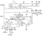
- the cleaning unit 16A includes a chamber (unit housing) 20A.
- a substrate holding mechanism 30 is provided in the chamber 20A.
- the substrate holding mechanism 30 includes a holding part 31, a support part 32, and a driving part 33.
- the substrate holding mechanism 30 rotates the support unit 32 by rotating the support unit 32 using the drive unit 33, thereby rotating the wafer W held by the support unit 31. .
- the processing liquid is supplied from the processing liquid supply unit 40 to the wafer W held by the substrate holding mechanism 30.
- the treatment liquid supply unit 40 includes a chemical liquid nozzle 41 that supplies a chemical liquid (for example, DHF, SC-1 and the like), a rinse nozzle 42 that supplies a rinsing liquid (for example, pure water (DIW)), and a solvent that can dissolve a sublimable substance (for example, a solvent nozzle 43 for supplying isopropyl alcohol (IPA)) and a sublimable substance solution nozzle 44 for supplying a sublimable substance solution (for example, an ammonium silicofluoride dissolved in a solvent, here, IPA) are provided.
- a chemical liquid for example, DHF, SC-1 and the like
- DIW pure water
- a solvent that can dissolve a sublimable substance for example, a solvent nozzle 43 for supplying isopropyl alcohol (IPA)
- IPA isopropyl alcohol
- IPA sublimable substance solution nozzle 44
- the nozzles 41 to 44 are connected to a corresponding processing liquid supply source (liquid storage tank or factory power) (not shown) via a supply line (not shown) connected thereto.
- a processing liquid supply source liquid storage tank or factory power
- Each supply line is provided with a flow rate adjusting device (not shown) such as an on-off valve or a flow rate control valve.
- the nozzles 41 to 44 are attached to the tip of the nozzle arm 45. By operating the nozzle arm 45, the nozzles 41 to 44 can be moved between a processing position directly above the center of the wafer W and a standby position outside the wafer W.
- FFU (Fan Filter Unit) 21 is provided on the ceiling of the chamber 20A.
- a flow rate adjusting valve such as a fan 23 and a damper 24 is interposed in the duct 22 of the FFU 21.
- the air is filtered by a filter such as a ULPA filter 25 provided below the outlet 22b of the duct 22, and then flows downward into the internal space of the chamber 20A.
- An FFU 21 and a gas supply unit 27 are provided as a gas supply mechanism for supplying gas into the chamber 20A.
- a rectifying plate 26 in the form of a punching plate is provided on the upper portion of the chamber 20A.
- the current plate 26 adjusts the distribution of clean air discharged downward from the FFU 21 into the chamber 20A.
- the gas supply unit 27 supplies gas to the space between the FFU 21 and the rectifying plate 26.
- the gas supply unit 27 includes a gas supply nozzle 27a.
- a clean, low-humidity gas such as nitrogen gas or dry air is supplied to the gas supply nozzle 27a from a gas supply source 27b through a gas supply line 27d provided with a flow control device 27c such as an on-off valve or a flow control valve. Is done.
- the FFU 21 and the gas supply unit 27 are examples of the gas supply mechanism, and the installation position, shape, gas supply amount, etc. of the gas supply mechanism may have various forms corresponding to the device structure. .
- the collection cup 50 is disposed so as to surround the holding portion 31 of the substrate holding mechanism 30.
- the collection cup 50 collects the processing liquid scattered from the wafer W.
- a drainage port 51 is formed at the bottom of the recovery cup 50, and the processing liquid collected by the recovery cup 50 is discharged from the drainage port 51 to the outside of the processing unit 16.
- An exhaust port 52 for discharging the atmosphere inside the recovery cup 50 to the outside of the processing unit 16 is formed at the bottom of the recovery cup 50.
- the exhaust through the exhaust port 52 is described as “cup exhaust (C-EXH)”.
- An exhaust path 53 is connected to the exhaust port 52 as an exhaust mechanism for exhausting the atmosphere inside the chamber 20A.
- the atmosphere in the recovery cup 50 is always sucked through the exhaust path 53 and the exhaust port 52, and the recovery cup 50 has a negative pressure. For this reason, after being supplied from the FFU 21, the clean flow that flows downward through the current plate 26 and reaches the space near the wafer W above the wafer W (hereinafter, referred to as “the upper space near the wafer” for the sake of simplicity). Air is drawn into the recovery cup 50 through the space between the peripheral wall of the upper opening of the recovery cup 50 and the outer peripheral edge of the wafer W (see arrow F in FIG. 2). The airflow suppresses the atmosphere (chemical solution atmosphere, solvent atmosphere) derived from the processing solution supplied to the wafer W from staying in the upper space near the wafer.
- the exhaust passage 53 branches into two branch passages 53a and 53b, and merges into one exhaust passage 53 again.
- the downstream end of the exhaust path 53 is connected to a decompressed factory exhaust system duct (not shown).
- One branch path 53a is provided with a normally open on-off valve 54a
- the other branch path 53b is provided with a normally closed on-off valve 54b.
- a flow rate adjusting valve 54 such as a damper or a butterfly valve may be provided in the exhaust path 53 as schematically shown in FIG.
- the flow rate of the exhaust gas flowing through the exhaust passage 53 can be adjusted by adjusting the opening degree of the flow rate adjusting valve 54.
- the flow rate (or flow velocity) of the gas (clean air) flowing in the upper space near the wafer can be changed.
- a flow rate adjustment valve 54 may be provided in the exhaust passage 53 upstream or downstream of the branch passages 53 a and 53 b.
- the installation position, shape, gas supply amount, and the like of the exhaust mechanism may have various forms corresponding to the device structure.
- a solvent concentration sensor 46 is attached to the tip of the nozzle arm 45.
- the solvent concentration sensor 46 can measure the solvent concentration (IPA concentration) in the upper space near the wafer.
- the recovery cup 50 is configured by combining a plurality of cup bodies (not shown), and different fluid passages are formed in the recovery cup 50 by changing the relative positional relationship of the plurality of cup bodies. Also good.
- the treatment liquid and the gas accompanying the treatment liquid are discharged from the recovery cup 50 through a fluid passage corresponding to the type of the treatment liquid (for example, an acidic treatment liquid, an alkaline treatment liquid, or an organic treatment liquid). Since such a configuration is well known to those skilled in the art, illustration and description thereof are omitted. In this case, it is only necessary that the exhaust flow rate at the time of performing the treatment using at least the organic treatment liquid (solvent, sublimable substance solution) can be adjusted as described above.
- An exhaust port 56 for exhausting the atmosphere outside the recovery cup 50 is provided in the lower part of the chamber 20A and outside the recovery cup 50.
- An exhaust path 57 connected to a duct of a factory exhaust system (not shown) is connected to the exhaust port 56.
- the exhaust passage 57 is provided with a flow rate adjusting valve 58 such as a damper or a butterfly valve.
- the bake unit 16B has a chamber 20B.
- a hot plate 61 in which a resistance heater 62 is incorporated is provided in the chamber 20B.
- a plurality of support pins 63 are provided on the upper surface of the hot plate 61.
- the support pins 63 support the peripheral edge of the lower surface of the wafer W, and a small gap is formed between the lower surface of the wafer W and the upper surface of the hot plate 61.
- An exhaust hood (cover) 64 that can be moved up and down is provided above the hot plate 61.
- An exhaust pipe 65 in which a sublimable substance recovery device 66 and a pump 67 are interposed is connected to an opening provided at the center of the exhaust hood 64.
- the sublimable substance recovery device 66 recovers the sublimable substance by cooling the exhaust gas flowing into the sublimable substance recovery apparatus 66 to precipitate the sublimable substance.
- a film forming a semiconductor device for example, a wafer W subjected to dry etching to give a pattern to an SiN film, is carried into the cleaning unit 16A by the substrate transfer device 17 and held horizontally by the substrate holding mechanism 30.
- the chemical solution nozzle 41 is positioned above the central portion of the wafer W rotated by the substrate holding mechanism 30, and the chemical solution for cleaning is supplied from the chemical solution nozzle 41 to the wafer W. Unnecessary substances such as etching residues and particles are removed from the surface of the wafer W (chemical solution cleaning step).
- the rinse nozzle 42 is positioned above the central portion of the wafer W while the wafer W is continuously rotated, and DIW as a rinse liquid is supplied from the rinse nozzle 42 to the wafer W, whereby The chemical solution and the reaction product generated in the previous step are removed (rinsing step).
- the solvent nozzle 43 is positioned above the center of the wafer W, and the IPA (that does not include the sublimable substance) (that is, the sublimable substance is dissolved) from the solvent nozzle 43.
- Solvent that can be supplied to the wafer W, and DIW on the wafer W is replaced with IPA (solvent supply step).
- FIG. That is, the entire pattern 100 (having the convex portions 101 and the concave portions 102 between the adjacent convex portions 101) formed on the surface of the wafer W is covered with the IPA liquid film.
- the sublimable substance solution nozzle 44 is positioned above the center of the wafer W, and the sublimable substance solution SL (that is, the sublimable substance is removed from the sublimable substance solution nozzle 44).
- a solution in which a sublimable substance is dissolved in IPA, which is a solvent that can be dissolved, is supplied to the wafer W, and the IPA on the wafer W is replaced with the sublimable substance solution SL (sublimation substance solution supply step). .
- IPA a solvent that can be dissolved
- the concave portion 102 is filled with the sublimable substance solution SL, and the entire pattern 100 formed on the surface of the wafer W is covered with the liquid film of the sublimable substance solution SL. Thereafter, by adjusting the rotation of the wafer W, the thickness of the liquid film of the sublimable substance solution SL (which determines the film thickness “t” of the sublimable substance film SS) is adjusted.
- the deposition step can be performed, for example, by naturally evaporating the solvent while rotating the wafer W (without supplying the liquid to the wafer W).
- the wafer W is heated by a heating means (not shown) (for example, a resistance heating heater or an LED heating lamp) that is built in the holding unit 31 of the substrate holding mechanism 30 or disposed in the vicinity of the wafer W. It is also possible to promote.
- the state at the end of the deposition step is shown in FIG. That is, the recess 102 is filled with the solid sublimable material film SS.
- the film thickness “t” of the sublimable material film SS is a value that does not expose the pattern 100 (that is, “t” is larger than the height “h” of the convex portion 101 of the pattern 100), and as much as possible. Small is desirable.
- the pattern 100 is not exposed to the ambient atmosphere due to liquid breakage between the chemical solution cleaning step and the rinsing step, between the rinsing step and the solvent supply step, and between the solvent supply step and the sublimable substance solution supply step. It is preferable that the end of the discharge period of the treatment liquid used in the previous process overlaps the start of the discharge period of the treatment liquid used in the subsequent process.
- the solvent concentration sensor 46 attached to the tip of the nozzle arm 45 causes The solvent (IPA) concentration is measured.
- IPA solvent
- the control device 4 increases the flow rate of the exhaust gas passing through the exhaust passage 53. This increase in the exhaust flow rate can be realized by opening the normally closed on-off valve 54b. In the case of the configuration of FIG. 3, the exhaust flow rate can be increased by increasing the opening degree of the flow rate adjustment valve 54.
- the flow rate of the gas drawn into the recovery cup 50 from the upper space near the wafer is increased, and the flow rate (or flow velocity) of the gas flowing in the upper space near the wafer is increased.
- the solvent vapor (IPA vapor) drifting in the upper space near the wafer is more strongly drawn into the recovery cup 50.
- the solvent concentration (IPA concentration) in the upper space near the wafer can be reduced.
- the increased exhaust flow rate of the exhaust passage 53 may be maintained until the deposition step is completed. By doing so, the solvent concentration in the upper space near the wafer can be more reliably maintained low. Instead, when the IPA concentration detected by the solvent concentration sensor 46 is less than a predetermined threshold (second threshold), the increased exhaust flow rate in the exhaust passage 53 may be returned to the original value. By doing so, factory power (factory exhaust system) can be used effectively.
- the first threshold and the second threshold may be the same value, but it is preferable from the viewpoint of control stability that the second threshold is smaller than the first threshold.
- the exhaust flow rate of the exhaust path 53 (cup exhaust gas exhaust flow rate) is increased, the pressure in the chamber 20A may decrease, and the atmosphere outside the chamber 20A may flow into the chamber 20A.
- (1) the exhaust flow rate of the exhaust path 57 (exhaust flow rate of the module exhaust) is decreased, (2) gas is supplied from the gas supply nozzle 27a of the gas supply unit 27, and the chamber 20A is supplied. Increase the total flow rate of gas to be supplied.
- At least one of the countermeasures such as increasing the total flow rate of the gas to be performed can be executed.
- the countermeasure (2) or (3) for increasing the gas supply flow rate into the chamber 20A is adopted, the downflow of the gas flowing into the upper space near the wafer increases, so the solvent concentration in the upper space near the wafer. Can be reduced more efficiently.
- the wafer W is unloaded from the cleaning unit 16A by the substrate transfer device 17 and loaded into the bake unit 16B.
- the exhaust hood 64 is lowered to cover the upper portion of the wafer W.
- the wafer W is heated to a temperature higher than the sublimation temperature of the sublimable substance by the heated hot plate 61 while sucking the upper space of the wafer W by the pump 67 interposed in the exhaust pipe 65 connected to the exhaust hood 64. Is heated.
- the sublimable substance on the wafer W is sublimated and removed from the wafer W (sublimable substance removing step).
- the state at the end of the sublimation substance removal step is shown in FIG. That is, the sublimation substance filled in the concave portion 102 is removed without causing the convex portion 101 of the pattern 100 to collapse.
- the wafer W is unloaded from the bake unit 16B by the substrate transfer device 17 and transferred to the original carrier C.
- a sound sublimable material film can be formed by increasing the flow rate (or flow velocity) of the gas flowing in the upper space near the wafer.
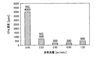
- FIG. 6 shows an exhaust flow rate of the exhaust passage (53) by performing a rinsing step, a solvent supply step, a sublimation substance solution supply step and a precipitation step using a processing unit substantially corresponding to the cleaning unit 16A shown in FIG. Then, a test was conducted to confirm the IPA concentration above the wafer W and the presence or absence of spotted defects.
- the exhaust flow rates were (Test 1) 0.45 m 3 / min, (Test 2) 0.53 m 3 / min, (Test 3) 0.65 m 3 / min, (Test 4) 0.90 m 3 / min, (Test 5) Five levels of 1.00 m 3 / min were set. In each test, while carrying out the solvent supply process, the sublimable substance solution supply process and the precipitation process, the above flow rate was kept constant. In each test, the IPA concentration was measured at a position 10 mm above the center of the wafer W.
- the occurrence of spotted defects can be prevented by suppressing the IPA concentration in the space above the wafer W in the vicinity of the wafer W to a predetermined value (500 ppm in this test) or less.
- a predetermined value 500 ppm in this test
- FIG. 8 shows an image when the spotted defect targeted in this embodiment is viewed from above the wafer.
- FIG. 9 is an image showing the relationship between the spotted defect and the pattern on the wafer. The pattern is not completely covered with the sublimable material film but is exposed.
- the mechanism of the occurrence of patchy defects is not clear at present, but the present inventor believes that it is one of the following. (Mechanism 1) When a relatively high concentration (for example, about 1000 ppm) of IPA vapor is present in the vicinity of the wafer surface, the film of the sublimable substance once deposited (solidified) is dissolved, and spotted defects are generated in the dissolved portion. .
- Mechanism 1 When a relatively high concentration (for example, about 1000 ppm) of IPA vapor is present in the vicinity of the wafer surface, the film of the sublimable substance once deposited (solidified) is dissolved, and spotted defects are generated in the dissolved portion. .
- Mechanism 2 When IPA vapor having a relatively high concentration (for example, about 1000 ppm) exists in the vicinity of the wafer surface, the evaporation of the solvent in the sublimable substance to be precipitated (solidified) is suppressed, thereby vaporizing. Since the heat is reduced, a large lump (large crystal) of the sublimable substance is precipitated (solidified), and a patch-like defect is generated at a crystal grain boundary portion having a large strain. It is clear from the above test results that the occurrence of spotted defects can be prevented by suppressing the IPA concentration in the vicinity of the wafer surface, regardless of whether the estimated mechanism of the spotted defects is correct or not.
- a relatively high concentration for example, about 1000 ppm
- the IPA concentration in the upper space near the wafer when the IPA concentration in the upper space near the wafer increases, the IPA concentration in the upper space near the wafer can be decreased by increasing the flow rate or flow velocity of the gas in the upper space near the wafer. it can. For this reason, it is possible to form a sound sublimable material film without defects.
- the exhaust flow rate of the recovery cup 50 is increased when the IPA concentration in the upper space near the wafer is increased, there may be a disadvantage that may occur when the exhaust flow rate of the recovery cup 50 is constantly kept high (for example, (1) below) (3)) can be avoided. That is, (1) the airflow in the recovery cup 50 can guide the processing liquid (in the form of mist) scattered from the wafer W after being supplied to the rotating wafer W to the drainage port in an intended manner. If the exhaust flow rate of the recovery cup 50 is increased more than necessary, the air flow in the recovery cup 50, particularly in the vicinity of the peripheral edge of the wafer W, is disturbed.
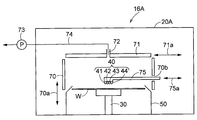
- a suction port 72 is provided in the top plate 71, and a space surrounded by the cylindrical body 70 and the top plate 71 can be sucked through the suction port 72 through an exhaust passage 74 in which a pump 73 is interposed.
- the nozzles 41 to 44 are provided at the tip of one or more rod-like nozzle arms 75, and the nozzle arms 75 are advanced into the space above the wafer through the openings 70b provided in the side peripheral wall of the cylindrical body 70 ( (See arrow 75a).
- an air flow toward the suction port 72 is formed in the upper space near the wafer, that is, the gas flow rate or flow velocity in the upper space near the wafer is increased, and the IPA concentration in the upper space near the wafer is increased. Can be reduced.
- the increase in the gas flow rate or flow velocity in the upper space near the wafer is performed when the detected value of the IPA concentration of the solvent concentration sensor 46 exceeds a predetermined threshold value.
- the processing conditions are the same, the elapsed time from the start of the supply period of the solvent-containing processing liquid in which the IPA concentration in the upper space near the wafer exceeds the threshold value is substantially the same. Therefore, an elapsed time that the IPA concentration is assumed to exceed the threshold value is obtained by experiment, and when the elapsed time arrives or slightly before the arrival, an increase in the gas flow rate or flow velocity in the space near the wafer starts.
- Process recipes may be created as described.
- the start of the increase is, for example, “simultaneous with the start of the solvent supply process”, “10 seconds after the start of the solvent supply process”, “simultaneous with the start of the sublimation substance solution supply process”, “5 In seconds ".
- the IPA concentration exceeds the threshold value in the precipitation step after the sublimable substance solution supply step, in that case, “simultaneous with the start of the precipitation step”, “5 seconds after the start of the precipitation step”, You may define as follows.
- the airflow change may be started a predetermined time before the start time of the supply period of the solvent-containing processing liquid so that the IPA concentration in the upper space near the wafer does not increase to the vicinity of the threshold.
- the start of the increase can be defined as, for example, “10 seconds before the start of the solvent supply process” or “10 seconds before the start of the sublimation substance solution supply process”.
- the substrate to be processed is not limited to the semiconductor wafer W described above, and may be another substrate such as an LCD glass substrate or a ceramic substrate.
- W substrate semiconductor wafer
- 24 Supply air flow rate adjustment unit air flow control unit (FFU21 fan, damper) 27c Supply air flow rate adjustment unit, air flow control unit (flow rate adjustment device 27c of gas supply unit 27) 30 Substrate holding part (substrate holding mechanism) 40 Treatment Solution Supply Unit 46 Concentration Measurement Unit (Solvent Concentration Sensor) 50 Enclosure (collection cup) 53,74 Exhaust line (exhaust passage) 54 Exhaust flow rate control unit, air flow control unit (flow control valve) 54a, 54b Exhaust flow rate adjustment unit, air flow control unit (open / close valve) 70, 71 Enveloping body (tubular body, top plate) 73 Exhaust flow rate control unit, air flow control unit (pump) 100 pattern 102 pattern recess
Landscapes
- Cleaning Or Drying Semiconductors (AREA)
Abstract
基板(W)に形成されたパターンの凹部に昇華性物質を満たす処理を行う基板処理装置は、基板を保持する基板保持部(30)と、昇華性物質を溶解しうる溶剤を含む少なくとも1種類の溶剤含有処理液を、基板に対して供給する処理液供給部(40)と基板保持部及び処理液供給部を収容するチャンバ(20)と、チャンバの内部に気体を供給する気体供給機構と、チャンバの内部の雰囲気を排気する排気機構と、を有する。処理液供給部が溶剤含有処理液を前記基板に供給している処理液供給期間内に、気体供給機構及び排気機構の少なくとも一方(例えば、排気路(53))を制御することによって基板の周囲の空間を流れる気流の流量または流速を増加させる気流変更を行う気流制御部(例えば、開閉弁(54a,54b))が設けられる。
Description
本発明は、基板に形成されたパターンの凹部に昇華性物質を満たす処理を行う技術に関する。
近年、半導体ウエハ等の基板に形成されるパターンの微細化に伴い、パターンのアスペクト比(高さ/幅)が高くなってきている。アスペクト比がある値より大きくなると、基板に対して半導体形成時の液処理後に行われる乾燥処理の際にパターン倒壊(パターンを構成する凸状部の倒壊)が生じやすくなる。
この問題を解決するため、パターンの凹部内にあるIPAを昇華性物質の溶液で置換する工程、その後、昇華性物質溶液中の溶剤を蒸発させてパターンの凹部内を固体状態の昇華性物質で満たす工程、その後、昇華性物質を昇華させる工程、という一連の工程を備えた乾燥方法が実行される(特許文献1を参照)。この方法は、液体の表面張力によるパターン倒壊を防止する上で有効である。
しかし、上記方法を用いた場合に、基板表面に斑が生じ、パターンが昇華性物質皮膜に完全に覆われずパターンの一部が露出することがある。これはパターン倒壊につながるため、回避しなければならない。
本発明は、昇華性物質の皮膜を基板全体に形成することができる技術を提供するものである。
本発明の一実施形態によれば、基板に形成されたパターンの凹部に昇華性物質を満たす処理を行う基板処理装置であって、基板を保持する基板保持部と、前記昇華性物質を溶解しうる溶剤を含む少なくとも1種類の溶剤含有処理液を、前記基板保持部に保持された前記基板に対して供給する処理液供給部と、前記基板保持部及び処理液供給部を収容するチャンバと、前記チャンバの内部に気体を供給する気体供給機構と、前記チャンバの内部の雰囲気を排気する排気機構と、前記処理液供給部が前記溶剤含有処理液を前記基板に供給している溶剤含有処理液の供給期間内又は前記供給期間の後に、前記気体供給機構及び前記排気機構の少なくとも一方を制御することによって前記基板の周囲の空間を流れる気流の流量または流速を増加させる気流変更を行う気流制御部と、を備えた基板処理装置が提供される。
本発明の他の実施形態によれば、基板を保持する基板保持部と、前記基板保持部に保持された前記基板に対して処理液を供給する処理液供給部と、前記基板保持部及び処理液供給部を収容するチャンバと、前記チャンバの内部に気体を供給する気体供給機構と、前記チャンバの内部の雰囲気を排気する排気機構と、を備える基板処理装置を用いて、前記基板に形成されたパターンの凹部に昇華性物質を満たす処理を行う基板処理方法であって、前記昇華性物質を溶解しうる溶剤を含む少なくとも1種類の溶剤含有処理液を、前記基板に対して供給する処理液供給工程と、前記昇華性物質を溶解しうる溶剤を含む溶剤含有処理液を前記基板に供給している溶剤含有処理液の供給期間内又は前記供給期間の後に、前記気体供給機構及び前記排気機構の少なくとも一方を制御することによって前記基板の周囲の空間を流れる気流の流量または流速を増加させる気流変更を行う気流変更工程と、を備えた基板処理方法が提供される。
本発明のさらに他の実施形態によれば、基板処理装置の動作を制御するためのコンピュータにより実行されたときに、前記コンピュータが前記基板処理装置を制御して上記の基板処理方法を実行させるプログラムが記録された記憶媒体が提供される。
上記本発明の実施形態によれば、基板の上方の空間の溶剤濃度を低く抑えることができるので、昇華性物質の皮膜を基板全体に形成することができる。
図1は、本実施形態に係る基板処理システムの概略構成を示す図である。以下では、位置関係を明確にするために、互いに直交するX軸、Y軸およびZ軸を規定し、Z軸正方向を鉛直上向き方向とする。
図1に示すように、基板処理システム1は、搬入出ステーション2と、処理ステーション3とを備える。搬入出ステーション2と処理ステーション3とは隣接して設けられる。
搬入出ステーション2は、キャリア載置部11と、搬送部12とを備える。キャリア載置部11には、複数枚のウエハWを水平状態で収容する複数のキャリアCが載置される。
搬送部12は、キャリア載置部11に隣接して設けられ、内部に基板搬送装置13と、受渡部14とを備える。基板搬送装置13は、ウエハWを保持する基板保持機構を備える。また、基板搬送装置13は、水平方向および鉛直方向への移動ならびに鉛直軸を中心とする旋回が可能であり、基板保持機構を用いてキャリアCと受渡部14との間でウエハWの搬送を行う。
処理ステーション3は、搬送部12に隣接して設けられる。処理ステーション3は、搬送部15と、複数の処理ユニット16とを備える。複数の処理ユニット16は、搬送部15の両側に並べて設けられる。
搬送部15は、内部に基板搬送装置17を備える。基板搬送装置17は、ウエハWを保持する基板保持機構を備える。また、基板搬送装置17は、水平方向および鉛直方向への移動ならびに鉛直軸を中心とする旋回が可能であり、基板保持機構を用いて受渡部14と処理ユニット16との間でウエハWの搬送を行う。
処理ユニット16は、基板搬送装置17によって搬送されるウエハWに対して所定の基板処理を行う。
また、基板処理システム1は、制御装置4を備える。制御装置4は、たとえばコンピュータであり、制御部18と記憶部19とを備える。記憶部19には、基板処理システム1において実行される各種の処理を制御するプログラムが格納される。制御部18は、記憶部19に記憶されたプログラムを読み出して実行することによって基板処理システム1の動作を制御する。
なお、かかるプログラムは、コンピュータによって読み取り可能な記憶媒体に記録されていたものであって、その記憶媒体から制御装置4の記憶部19にインストールされたものであってもよい。コンピュータによって読み取り可能な記憶媒体としては、たとえばハードディスク(HD)、フレキシブルディスク(FD)、コンパクトディスク(CD)、マグネットオプティカルディスク(MO)、メモリカードなどがある。
上記のように構成された基板処理システム1では、まず、搬入出ステーション2の基板搬送装置13が、キャリア載置部11に載置されたキャリアCからウエハWを取り出し、取り出したウエハWを受渡部14に載置する。受渡部14に載置されたウエハWは、処理ステーション3の基板搬送装置17によって受渡部14から取り出されて、処理ユニット16へ搬入される。
処理ユニット16へ搬入されたウエハWは、処理ユニット16によって処理された後、基板搬送装置17によって処理ユニット16から搬出されて、受渡部14に載置される。そして、受渡部14に載置された処理済のウエハWは、基板搬送装置13によってキャリア載置部11のキャリアCへ戻される。
次に、図2~図4を参照して処理ユニット16の構成について説明する。本実施形態では、基板処理システム1に含まれる処理ユニット16は、洗浄ユニット16Aと、ベークユニット16Bとを含む。図1では洗浄ユニット16Aとベークユニット16Bとを区別していないが、例えば、処理ステーション3の図1中上側にある処理ユニット16を洗浄ユニット16A、図1中下側にある処理ユニット16をベークユニット16Bとすることができる。
図2に示すように、洗浄ユニット16Aは、チャンバ(ユニットハウジング)20Aを備えている。チャンバ20A内には、基板保持機構30が設けられている。 基板保持機構30は、保持部31と、支柱部32と、駆動部33とを備える。かかる基板保持機構30は、駆動部33を用いて支柱部32を回転させることによって支柱部32に支持された保持部31を回転させ、これにより、保持部31に保持されたウエハWを回転させる。
基板保持機構30により保持されたウエハWに、処理液供給部40から処理液が供給される。処理液供給部40は、薬液(例えばDHF、SC-1等)を供給する薬液ノズル41、リンス液(例えば純水(DIW))を供給するリンスノズル42、昇華性物質を溶解しうる溶剤(例えばイソプロピルアルコール(IPA))を供給する溶剤ノズル43、および昇華性物質溶液(例えばケイフッ化アンモニウムを溶剤ここではIPAに溶解させたもの)を供給する昇華性物質溶液ノズル44を備えている。
上記のノズル41~44は、各々に接続された供給ライン(図示せず)を介して対応する処理液の供給源(液貯留タンクまたは工場用力)(図示せず)に接続されている。各供給ラインには、開閉弁、流量制御弁等の流量調節機器(図示せず)が介設されている。また、上記のノズル41~44は、ノズルアーム45の先端に取り付けられている。ノズルアーム45を動作させることにより、ノズル41~44をウエハW中心部の真上の処理位置と、ウエハWの外方の待機位置との間で移動させることができる。
チャンバ20Aの天井部には、FFU(Fan Filter Unit)21が設けられる。FFU21のダクト22には、ファン23およびダンパ24等の流量調整弁が介設されている。ファン23を回転させることにより、ダクト22の吸引口22aからクリーンルーム内の空気がダクト22内に流入する。空気は、ダクト22の出口22bの下方に設けられたULPAフィルタ25等のフィルタにより濾過された後、チャンバ20Aの内部空間に下向きに流出する。
チャンバ20Aの内部に気体を供給する気体供給機構としてFFU21と気体供給部27が設けられている。チャンバ20Aの上部には、パンチングプレートの形態の整流板26が設けられている。整流板26は、FFU21からチャンバ20A内に下向きに吐出された清浄空気の分布を調節する。気体供給部27は、FFU21と整流板26との間の空間に気体を供給する。気体供給部27は、気体供給ノズル27aを有する。気体供給ノズル27aには、気体供給源27bから、開閉弁、流量制御弁等の流量調節機器27cが介設された気体供給ライン27dを介して窒素ガスまたはドライエア等の清浄な低湿度気体が供給される。気体供給部27を、FFU21のダクト22内(ダンパ24の下流側)に気体を供給するように設けてもよい。なお、FFU21と気体供給部27は、気体供給機構の一例であって、気体供給機構の設置位置、形状、気体供給量等は、装置構造に対応して様々な形態を有していてもよい。
基板保持機構30の保持部31を取り囲むように回収カップ50が配置されている。回収カップ50は、ウエハWから飛散する処理液を捕集する。回収カップ50の底部には排液口51が形成されており、回収カップ50によって捕集された処理液は、排液口51から処理ユニット16の外部へ排出される。また、回収カップ50の底部には、回収カップ50内部の雰囲気を処理ユニット16の外部へ排出する排気口52が形成されている。ここでは、排気口52を介した排気は「カップ排気(C-EXH)」と記載する。
チャンバ20Aの内部の雰囲気を排気する排気機構として、排気口52には、排気路53が接続されている。回収カップ50内の雰囲気は、常時、排気路53および排気口52を介して吸引され、回収カップ50内は負圧となっている。このため、FFU21から供給された後に整流板26を通って下向きに流れ、ウエハWの上方のウエハWの近傍の空間(以下、簡便のため、「ウエハ近傍上方空間」と呼ぶ)に到達した清浄空気が、回収カップ50の上部開口部の周壁とウエハWの外周縁との間を通って回収カップ50内に引き込まれる(図2の矢印Fを参照)。上記の気流により、ウエハWに供給された処理液由来の雰囲気(薬液雰囲気、溶剤雰囲気)がウエハ近傍上方空間に滞留することが抑制されている。
排気路53は2つの分岐路53a,53bに分岐し、再び1つの排気路53に合流している。排気路53の下流端は減圧された工場排気系のダクト(図示せず)に接続されている。一方の分岐路53aにノーマルオープンの開閉弁54aが設けられ、他方の分岐路53bにノーマルクローズの開閉弁54bが設けられている。開閉弁54bを開くことにより、排気路53を流れる排気(カップ排気)の流量が増大し、回収カップ50内の圧力が下がる。その結果、回収カップ50内に引き込まれる気体の流量が増え、ウエハ近傍上方空間を流れる気体(清浄空気)の流量(または流速)を増大させることができる。
2つの分岐路53a,53bを設けることに代えて、図3に概略的に示すように、排気路53に、ダンパまたはバタフライ弁等の流量調整弁54を設けてもよい。この場合、流量調整弁54の開度を調節することにより、排気路53を流れる排気の流量を調節することができる。この場合も、ウエハ近傍上方空間を流れる気体(清浄空気)の流量(または流速)を変化させることができる。図2の構成において、分岐路53a,53bの上流側または下流側の排気路53に流量調整弁54を設けてもよい。なお、上記の排気路53の構造に限らず、排気機構の設置位置、形状、気体供給量等は、装置構造に対応して様々な形態を有していてもよい。
ノズルアーム45の先端部には、溶剤濃度センサ46が取り付けられている。溶剤濃度センサ46により、ウエハ近傍上方空間内の溶剤濃度(IPA濃度)を測定することができる。
回収カップ50を、複数のカップ体(図示せず)を組み合わせて構成し、これら複数のカップ体の相対的位置関係を変更することによって回収カップ50内に異なる流体通路が形成されるようにしてもよい。この場合、処理液(例えば酸性処理液、アルカリ性処理液、有機系処理液)の種類に応じた流体通路を通って、処理液および当該処理液に随伴する気体が回収カップ50から排出される。このような構成は当業者において周知であるので、図示及び説明は省略する。この場合、少なくとも有機系処理液(溶剤、昇華性物質溶液)を用いた処理を行うときの排気流量が、上記のように調節可能であればよい。
チャンバ20Aの下部であって回収カップ50の外側には、回収カップ50の外側の雰囲気を排気する排気口56が設けられている。排気口56には、図示しない工場排気系のダクトに接続された排気路57が接続されている。排気路57には、ダンパまたはバタフライ弁等の流量調整弁58が設けられている。排気口56からチャンバ20Aの内部空間の雰囲気を排出することにより、回収カップ50の外側に薬液雰囲気または有機雰囲気が滞留することを防止することができる。ここでは、排気口56を介した排気は、「モジュール排気(M-EXH)」と記載する。
次にベークユニット16Bについて図4を参照して簡単に説明する。ベークユニット16Bは、チャンバ20Bを有する。チャンバ20B内には、抵抗加熱ヒーター62が内蔵された熱板61が設けられている。熱板61上面には複数の支持ピン63が設けられている。支持ピン63はウエハWの下面周縁部を支持し、ウエハWの下面と熱板61の上面との間に小さな隙間が形成される。熱板61の上方に、昇降移動可能な排気用フード(覆い)64が設けられる。排気用フード64の中心に設けられた開口部に、昇華性物質回収装置66およびポンプ67が介設された排気管65が接続されている。昇華性物質回収装置66は、昇華性物質回収装置66に流入してきた排気を冷却して昇華性物質を析出させることにより、昇華性物質を回収する。
次に、上述の洗浄ユニット16Aおよびベークユニット16Bを備えた基板処理システム1により実行される一連の処理について説明する。以下の一連の処理は、制御装置4(図1参照)の制御の下で自動的に実行される。
半導体装置を形成する膜、例えばSiN膜にパターンを付与するためにドライエッチングを施したウエハWが、基板搬送装置17により洗浄ユニット16Aに搬入され、基板保持機構30により水平に保持される。
まず、基板保持機構30により回転させられているウエハWの中心部の上方に薬液ノズル41を位置させ、この薬液ノズル41から洗浄用の薬液をウエハWに供給することにより、前工程で生じたエッチング残渣、パーティクル等の不要物質をウエハW表面から除去する(薬液洗浄工程)。
次に、引き続きウエハWを回転させたまま、ウエハWの中心部の上方にリンスノズル42を位置させ、このリンスノズル42からリンス液としてのDIWをウエハWに供給することにより、ウエハW上の薬液および前工程で生じた反応生成物が除去される(リンス工程)。
次に、引き続きウエハWを回転させたまま、ウエハWの中心部の上方に溶剤ノズル43を位置させて、この溶剤ノズル43から(昇華性物質を含まない)IPA(つまり昇華性物質を溶解することができる溶剤)がウエハWに供給されて、ウエハW上のDIWがIPAに置換される(溶剤供給工程)。このときの状態が図5(a)に示されている。つまり、ウエハWの表面に形成されたパターン100(凸部101と、隣接する凸部101間の凹部102とを有する)の全体が、IPAの液膜に覆われている。
次に、引き続きウエハWを回転させたまま、ウエハWの中心部の上方に昇華性物質溶液ノズル44を位置させて、この昇華性物質溶液ノズル44から昇華性物質溶液SL(つまり昇華性物質を溶解することができる溶剤であるIPAに昇華性物質を溶解させた溶液)がウエハWに供給されて、ウエハW上にあるIPAを昇華性物質溶液SLで置換する(昇華性物質溶液供給工程)。このときの状態が図5(b)に示されている。つまり、凹部102には昇華性物質溶液SLが充填され、ウエハWの表面に形成されたパターン100の全体が、昇華性物質溶液SLの液膜に覆われている。その後、ウエハWの回転を調整することにより、昇華性物質溶液SLの液膜の厚さ(これにより昇華性物質膜SSの膜厚「t」が決まる)を調節する。
次に、昇華性物質溶液中の溶剤を蒸発させて、昇華性物質を析出(固化)させ、固体の昇華性物質膜SSを形成する(析出工程)。析出工程は、例えば、(ウエハWに対する液の供給を行わないで)ウエハWを回転させながら溶剤を自然に蒸発させることにより行うことができる。基板保持機構30の保持部31に内蔵されるか、あるいは、ウエハW近傍に配置された図示しない加熱手段(例えば抵抗加熱ヒーターまたはLED加熱ランプ)等により、ウエハWを暖めることにより、析出工程を促進することも可能である。析出工程の終了時の状態が図5(c)に示されている。つまり、凹部102に固体の昇華性物質膜SSが充填されている。昇華性物質膜SSの膜厚「t」は、パターン100が露出しないような値であって(つまり、「t」がパターン100の凸部101の高さ「h」より大きい)、かつ、なるべく小さいことが望ましい。
上述した薬液洗浄工程とリンス工程との間、リンス工程と溶剤供給工程との間、溶剤供給工程と昇華性物質溶液供給工程との間で液切れによりパターン100が周囲雰囲気中に露出しないように、前工程で用いる処理液の吐出期間の終期と、後工程で用いる処理液の吐出期間の始期とをオーバーラップさせることが好ましい。
上述した薬液洗浄工程、リンス工程、溶剤供給工程、昇華性物質溶液供給工程および析出工程を実施している間、ノズルアーム45の先端部に取り付けられた溶剤濃度センサ46により、ウエハ近傍上方空間内の溶剤(IPA)濃度が計測されている。溶剤濃度の計測値が予め定められた閾値(第1閾値)例えば500ppmを超えると、制御装置4は、排気路53を通る排気の流量を増加させる。この排気流量の増加は、ノーマルクローズの開閉弁54bを開くことにより実現することができる。なお、図3の構成の場合には、流量調整弁54の開度を大きくすることにより排気流量を増加させることができる。
排気路53の排気流量を増加させることにより、前述したように、ウエハ近傍上方空間から回収カップ50内に引き込まれる気体の流量が増加し、ウエハ近傍上方空間を流れる気体の流量(または流速が)増加し、ウエハ近傍上方空間内を漂う溶剤蒸気(IPA蒸気)が回収カップ50内により強く引き込まれるようになる。その結果、ウエハ近傍上方空間内の溶剤濃度(IPA濃度)を低下させることができる。
増大させた排気路53の排気流量は、析出工程が終了するまで維持してもよい。そうすることにより、より確実にウエハ近傍上方空間内の溶剤濃度を低く維持することができる。これに代えて、溶剤濃度センサ46により検出されたIPA濃度が予め定められた閾値(第2閾値)未満となったら、増大させた排気路53の排気流量を元に戻してもよい。そうすることにより、工場用力(工場排気系)を有効利用することができる。なお、上記第1閾値と第2閾値は同じ値でもよいが、第2閾値を第1閾値よりも小さくすることが制御の安定性の観点から好ましい。
なお、排気路53の排気流量(カップ排気の排気流量)を増加させると、チャンバ20A内の圧力が低下し、チャンバ20A内にチャンバ20A外部の雰囲気が流入するおそれがある。この問題を解消するために、(1)排気路57の排気流量(モジュール排気の排気流量)を減少させる、(2)気体供給部27の気体供給ノズル27aから気体を供給し、チャンバ20A内に供給される気体の総流量を増やす、(3)FFU21が各チャンバ20Aへの気体供給流量を個別的に制御できるならば、(例えばファン23またはダンパ24の制御により)FFU21からチャンバ20A内に供給される気体の総流量を増やす、等の対応策の少なくともいずれか一つを実行することができる。チャンバ20A内への気体供給流量を増やす対応策(2)または(3)を採用した場合には、ウエハ近傍上方空間に流入する気体のダウンフローが増加するため、ウエハ近傍上方空間内の溶剤濃度をより効率良く低下させることができる。
析出工程が終了したら、基板搬送装置17により、洗浄ユニット16AからウエハWを搬出し、ベークユニット16Bに搬入する。次いで、排気用フード64が下降してウエハWの上方を覆う。排気用フード64に接続された排気管65に介設されたポンプ67によりウエハWの上方空間を吸引しながら、昇温された熱板61により昇華性物質の昇華温度よりも高い温度にウエハWが加熱される。これにより、ウエハW上の昇華性物質は昇華して、ウエハWから除去される(昇華性物質除去工程)。
昇華性物質除去工程の終了時の状態が図5(d)に示されている。つまり、パターン100の凸部101の倒壊を生じさせることなく、凹部102に充填されていた昇華性物質が除去されている。昇華性物質除去工程の終了後、ウエハWは、基板搬送装置17により、ベークユニット16Bから搬出され、元のキャリアCに搬送される。
次に、ウエハ近傍上方空間を流れる気体の流量(または流速を)増加させることにより、健全な昇華性物質膜が形成できることについて説明する。
図6は、図2に示した洗浄ユニット16Aに概ね相当する処理ユニットを用いて、リンス工程、溶剤供給工程、昇華性物質溶液供給工程および析出工程を実施し、排気路(53)の排気流量、ウエハW上方のIPA濃度、及び斑状欠陥の発生の有無について確認する試験を行った。
排気流量は、(試験1)0.45m3/min、(試験2)0.53m3/min、(試験3)0.65m3/min、(試験4)0.90m3/min、(試験5)1.00m3/minの5水準とした。各試験において、溶剤供給工程、昇華性物質溶液供給工程および析出工程を実施している間、上記の流量で一定に維持した。各試験において、ウエハWの中心部の上方10mmの位置でIPA濃度を測定した。
試験結果を図6のグラフに示す。排気流量が0.45m3/min、0.53m3/minのとき、IPA濃度の最大値(溶剤供給工程、昇華性物質溶液供給工程および析出工程の全期間における最大値)がそれぞれ4000ppm、800ppmであり、いずれの場合も昇華性物質の膜の表面に斑状欠陥が発生していた(NG)。一方、排気流量が0.65m3/min、0.90m3/min、1.00m3/minのときのIPA濃度は、それぞれ300ppm、300ppm、500ppmであり、いずれの場合も昇華性物質の膜の表面に斑状欠陥は発生していなかった。このことから、少なくともウエハWの近傍のウエハWの上方の空間のIPA濃度を所定値(この試験では500ppm)以下に抑えることにより、斑状欠陥の発生を防止できることがわかった。そして、そのためには、排気流量を所定値(この試験では)0.65m3/min以上とすることが有効であることがわかった。斑状欠陥の発生を防止することができる排気流量は、チャンバ20の内容積や昇華性物質溶液の濃度により変化するものと考えられる。
本実施形態で対象とする斑状欠陥をウエハの上方から見た場合のイメージ図を図8に示す。また、図9は斑状欠陥とウエハ上のパターンとの関係を示したイメージ図であり、パターンが昇華性物質皮膜に完全に覆われておらず露出している。斑状欠陥の発生のメカニズムは、現時点では明確ではないが、本件発明者は以下のいずれかであると考えている。(メカニズム1)ウエハ表面近傍に比較的高濃度(例えば1000ppm程度)のIPA蒸気が存在していると、一旦析出(固化)した昇華性物質の膜を溶解させ、溶解した部分に斑状欠陥が生じる。(メカニズム2)ウエハ表面近傍に比較的高濃度(例えば1000ppm程度)のIPA蒸気が存在していると、析出(固化)しようとしている昇華性物質の中の溶剤の蒸発が抑制されることにより気化熱が低下するため、昇華性物質の大きな塊(大きな結晶)が析出(固化)し、歪みが大きい結晶粒界部に斑状欠陥が生じる。推定される斑状欠陥のメカニズムが正しいか否かに関わらず、ウエハ表面近傍のIPA濃度を抑制することにより斑状欠陥の発生を防止できることは、上記試験結果より明らかである。
上記実施形態によれば、ウエハ近傍上方空間内のIPA濃度が増加したときにウエハ近傍上方空間内の気体の流量または流速を増加させることにより、ウエハ近傍上方空間内のIPA濃度を減少させることができる。このため、欠陥の無い健全な昇華性物質の膜を形成することができる。
また、ウエハ近傍上方空間内のIPA濃度が増加したときに回収カップ50の排気流量を増大させるので、回収カップ50の排気流量を常に高く維持する場合に生じうる不利益(例えば下記の(1)~(3))を回避することができる。すなわち、(1)回収カップ50内の気流は、回転するウエハWに供給された後にウエハWから飛散する処理液(ミスト状になる)を、意図した態様で排液口に導くことができるように設定されており、回収カップ50の排気流量を必要以上に高めることは、回収カップ50内、特にウエハWの周縁部近傍の気流を乱すことになる。また、(2)多くの処理ユニットで共用している排気系の吸引力を一つの処理ユニットで多量に利用することは、限られた工場用力の有効利用という観点から好ましくない。求められる排気流量を達成するため、工場排気系の能力を増加させるか、あるいは基板処理システム1専用の排気ポンプを新設しなければならない場合もある。(3)チャンバ20A内の圧力低下を防止するため、排気流量に相当する供給流量で気体をチャンバ20A内に供給する際に、工場用力が余分に消費される。
上記実施形態では、回収カップ50の排気流量を増大させることにより、ウエハ近傍上方空間内のIPA濃度を減少させた。つまり、ウエハWの下方の空間の吸引量を増大させることにより、ウエハ近傍上方空間内の気体の流量または流速を増加させた。しかしながら、これには限定されるものではなく、ウエハWの上方の空間を吸引することにより、ウエハ近傍上方空間内の気体の流量または流速を増加させてもよい。
具体的には、例えば、図7に概略的に示すように、回収カップ50の外側に回収カップ50の外側を囲む筒状体70を設け、さらに筒状体70の上部開口を概ね閉塞する天板71を設ける。筒状体70は昇降可能(矢印70a参照)とし、使用しないときには下降位置に退避できるようにする。天板71も、上昇位置にある筒状体70の上部開口を閉鎖する閉鎖位置と、閉鎖位置から退避した退避位置との間を移動可能(矢印71a参照)とする。天板71に吸引口72を設け、吸引口72を介して、筒状体70と天板71とによって囲まれた空間を、ポンプ73が介設された排気路74を介して吸引可能とする。この場合、ノズル41~44は、1つ以上の棒状のノズルアーム75の先端に設け、ノズルアーム75を筒状体70の側周壁に設けた開口70bを介してウエハの上方の空間に進出(矢印75a参照)できるようにする。ポンプ73を動作させることにより、ウエハ近傍上方空間内に吸引口72に向かう気流が形成され、つまり、ウエハ近傍上方空間内の気体の流量または流速が増大し、ウエハ近傍上方空間内のIPA濃度を低下させることができる。
上記実施形態においては、ウエハ近傍上方空間内の気体の流量または流速の増加は、溶剤濃度センサ46のIPA濃度の検出値が所定の閾値を超えたときに行った。しかしながら、処理条件が同じならば、ウエハ近傍上方空間のIPA濃度が閾値を超える溶剤含有処理液の供給期間の開始からの経過時間は概ね同じである。従って、IPA濃度が閾値を超えると想定される経過時間を実験により求めておき、その経過時間が到来したときや到来よりも少し前にウエハ近傍上方空間内の気体の流量または流速の増加が開始されるようにプロセスレシピを作成してもよい。上記の増加開始は、例えば、「溶剤供給工程開始と同時」、「溶剤供給工程開始から10秒後」、「昇華性物質溶液供給工程開始と同時」、「昇華性物質溶液供給工程開始から5秒後」、のように定義することができる。また、昇華性物質溶液供給工程の後である析出工程においてIPA濃度が閾値を超えることも想定されるので、その場合は、「析出工程開始と同時」、「析出工程開始から5秒後」、のように定義してもよい。一方、そもそもウエハ近傍上方空間のIPA濃度が閾値の近傍まで上昇することがないように、溶剤含有処理液の供給期間の開始時間から所定時間前に気流変更を開始するようにしてもよい。上記の増加開始は、例えば、「溶剤供給工程開始の10秒前」や、「昇華性物質溶液供給工程開始の10秒前」、のように定義することができる。
上記実施形態においては、リンス工程の後に、溶剤供給工程を行ってから昇華性物質溶液供給工程を行ったが、リンス工程の後に溶剤供給工程を行わずに昇華性物質溶液供給工程を実行することも可能である。この場合、パターンの凹部に昇華性物質を満たす処理を行うために用いられる溶剤含有処理液(昇華性物質を溶解しうる溶剤を含む溶液)は1種類(昇華性物質溶液のみ)である。これに対して、前述した実施形態においては、パターンの凹部に昇華性物質を満たす処理を行うために用いられる溶剤含有処理液は、溶剤(昇華性物質を含まない)と、昇華性物質溶液の2種類である。
処理対象の基板は、上述した半導体ウエハWに限定されるものではなく、LCD用ガラス基板、セラミック基板等の他の基板であってもよい。
W 基板(半導体ウエハ)
23,24 給気流量調節部、気流制御部(FFU21のファン、ダンパ)
27c 給気流量調節部、気流制御部(気体供給部27の流量調節機器27c)
30 基板保持部(基板保持機構)
40 処理液供給部
46 濃度計測部(溶剤濃度センサ)
50 包囲体(回収カップ)
53,74 排気ライン(排気路)
54 排気流量調節部、気流制御部(流量制御弁)
54a,54b 排気流量調節部、気流制御部(開閉弁)
70,71 包囲体(筒状体、天板)
73 排気流量調節部、気流制御部(ポンプ)
100 パターン
102 パターンの凹部
23,24 給気流量調節部、気流制御部(FFU21のファン、ダンパ)
27c 給気流量調節部、気流制御部(気体供給部27の流量調節機器27c)
30 基板保持部(基板保持機構)
40 処理液供給部
46 濃度計測部(溶剤濃度センサ)
50 包囲体(回収カップ)
53,74 排気ライン(排気路)
54 排気流量調節部、気流制御部(流量制御弁)
54a,54b 排気流量調節部、気流制御部(開閉弁)
70,71 包囲体(筒状体、天板)
73 排気流量調節部、気流制御部(ポンプ)
100 パターン
102 パターンの凹部
Claims (15)
- 基板に形成されたパターンの凹部に昇華性物質を満たす処理を行う基板処理装置であって、
基板を保持する基板保持部と、
前記昇華性物質を溶解しうる溶剤を含む少なくとも1種類の溶剤含有処理液を、前記基板保持部に保持された前記基板に対して供給する処理液供給部と、
前記基板保持部及び処理液供給部を収容するチャンバと、
前記チャンバの内部に気体を供給する気体供給機構と、
前記チャンバの内部の雰囲気を排気する排気機構と、
前記処理液供給部が前記溶剤含有処理液を前記基板に供給している溶剤含有処理液の供給期間内又は前記供給期間の後に、前記気体供給機構及び前記排気機構の少なくとも一方を制御することによって前記基板の周囲の空間を流れる気流の流量または流速を増加させる気流変更を行う気流制御部と、
を備えた基板処理装置。 - 前記排気機構として前記基板保持部に保持された前記基板の周囲の雰囲気を排気する排気ラインを備え、前記気流制御部は、前記排気ラインを流れる排気の流量を調節する排気流量調節部を含み、前記気流制御部は、前記排気ラインを流れる排気の流量を調節することにより前記気流変更を行う、請求項1に記載の基板処理装置。
- 前記基板保持部により保持された前記基板の周囲を囲む包囲体をさらに備え、前記排気ラインは前記包囲体に接続されて前記包囲体内の雰囲気を排気し、これにより前記基板の上方の空間の雰囲気を吸引する、請求項2記載の基板処理装置。
- 前記気体供給機構として前記基板保持部により保持された前記基板の上方の空間に気体を供給する気体供給部を備え、前記気流制御部は、前記気体供給部から供給される気体の流量を調節する給気流量調節部を含み、前記気流制御部は、前記気体供給部から供給される気体の流量を増加させることにより前記気流変更を行う、請求項1記載の基板処理装置。
- 前記基板保持部に保持された基板の上方の空間の溶剤の濃度を計測する濃度計測部をさらに備え、
前記気流制御部は、前記濃度計測部により計測された溶剤の濃度値に応じて前記気流変更を行う、請求項1記載の基板処理装置。 - 前記基板保持部に保持された基板の上方の空間の溶剤の濃度を計測する濃度計測部をさらに備え、
前記気流制御部は、前記濃度計測部により計測された溶剤の濃度値に応じて前記気流変更を行う、請求項2記載の基板処理装置。 - 前記処理液供給部は、前記溶剤含有処理液として、前記昇華性物質を含まない前記溶剤及び昇華性物質溶液の両方を基板に供給するように構成され、
前記処理液供給部は、前記昇華性物質を含まない前記溶剤を前記基板に供給した後に、前記昇華性物質溶液を前記基板に供給する、請求項1から6のうちのいずれか一項に記載の基板処理装置。 - 基板を保持する基板保持部と、前記基板保持部に保持された前記基板に対して処理液を供給する処理液供給部と、前記基板保持部及び処理液供給部を収容するチャンバと、前記チャンバの内部に気体を供給する気体供給機構と、前記チャンバの内部の雰囲気を排気する排気機構と、を備える基板処理装置を用いて、前記基板に形成されたパターンの凹部に昇華性物質を満たす処理を行う基板処理方法であって、
前記昇華性物質を溶解しうる溶剤を含む少なくとも1種類の溶剤含有処理液を、前記基板に対して供給する処理液供給工程と、
前記昇華性物質を溶解しうる溶剤を含む溶剤含有処理液を前記基板に供給している溶剤含有処理液の供給期間内又は前記供給期間の後に、前記気体供給機構及び前記排気機構の少なくとも一方を制御することによって前記基板の周囲の空間を流れる気流の流量または流速を増加させる気流変更を行う気流変更工程と、
を備えた基板処理方法。 - 前記気流変更工程は、前記排気機構である前記基板の周囲の雰囲気を排気する排気ラインを流れる排気の流量を増加させることを含む、請求項8に記載の基板処理方法。
- 前記排気ラインは、前記基板の周囲を囲む包囲体内の雰囲気を排気し、これにより前記基板の上方の空間の雰囲気が吸引される、請求項9記載の基板処理方法。
- 前記気流変更工程は、前記気体供給機構によって前記基板の上方の空間に供給される気体の流量を調節することを含む、請求項8記載の基板処理方法。
- 前記気流変更工程は、前記基板保持部に保持された基板の上方の空間の溶剤の濃度を計測する濃度計測部により得られる濃度の計測値に応じて前記気流変更を行う、請求項8記載の基板処理方法。
- 前記気流変更工程は、前記基板保持部に保持された基板の上方の空間の溶剤の濃度を計測する濃度計測部により得られる濃度の計測値に応じて前記気流変更を行う、請求項9記載の基板処理方法。
- 前記処理液供給工程は、前記昇華性物質を含まない前記溶剤を前記基板に供給する溶剤供給工程と、その後に前記昇華性物質を溶解しうる溶剤に前記昇華性物質を溶解してなる昇華性物質溶液を基板に供給する昇華性物質溶液供給工程とを含む、請求項8から13のうちのいずれか一項記載の基板処理方法。
- 基板処理装置の動作を制御するためのコンピュータにより実行されたときに、前記コンピュータが前記基板処理装置を制御して請求項8記載の基板処理方法を実行させるプログラムが記録された記憶媒体。
Priority Applications (1)
| Application Number | Priority Date | Filing Date | Title |
|---|---|---|---|
| JP2018533563A JP6728358B2 (ja) | 2016-08-12 | 2017-08-10 | 基板処理装置、基板処理方法および記憶媒体 |
Applications Claiming Priority (2)
| Application Number | Priority Date | Filing Date | Title |
|---|---|---|---|
| JP2016-158945 | 2016-08-12 | ||
| JP2016158945 | 2016-08-12 |
Publications (1)
| Publication Number | Publication Date |
|---|---|
| WO2018030516A1 true WO2018030516A1 (ja) | 2018-02-15 |
Family
ID=61162894
Family Applications (1)
| Application Number | Title | Priority Date | Filing Date |
|---|---|---|---|
| PCT/JP2017/029096 Ceased WO2018030516A1 (ja) | 2016-08-12 | 2017-08-10 | 基板処理装置、基板処理方法および記憶媒体 |
Country Status (2)
| Country | Link |
|---|---|
| JP (1) | JP6728358B2 (ja) |
| WO (1) | WO2018030516A1 (ja) |
Cited By (8)
| Publication number | Priority date | Publication date | Assignee | Title |
|---|---|---|---|---|
| WO2020004214A1 (ja) * | 2018-06-29 | 2020-01-02 | 株式会社Screenホールディングス | 基板処理装置および基板処理方法 |
| JP2020004948A (ja) * | 2018-06-22 | 2020-01-09 | 株式会社Screenホールディングス | 基板処理方法、基板処理装置、および乾燥前処理液 |
| WO2020166136A1 (ja) * | 2019-02-14 | 2020-08-20 | 株式会社Screenホールディングス | 基板乾燥方法および基板処理装置 |
| JP2020136313A (ja) * | 2019-02-13 | 2020-08-31 | 株式会社Screenホールディングス | 基板処理方法および基板処理装置 |
| JP2020167189A (ja) * | 2019-03-28 | 2020-10-08 | 株式会社Screenホールディングス | 基板処理装置、基板処理方法、および、半導体製造方法 |
| JP2022035122A (ja) * | 2020-08-20 | 2022-03-04 | 株式会社Screenホールディングス | 基板処理装置および基板処理方法 |
| JP2022145824A (ja) * | 2018-12-28 | 2022-10-04 | 株式会社Screenホールディングス | 基板処理方法および基板処理装置 |
| JP2024055544A (ja) * | 2022-10-07 | 2024-04-18 | 株式会社Screenホールディングス | 基板処理方法及び基板処理装置 |
Families Citing this family (1)
| Publication number | Priority date | Publication date | Assignee | Title |
|---|---|---|---|---|
| US11124869B2 (en) | 2018-06-22 | 2021-09-21 | SCREEN Holdings Co., Ltd. | Substrate processing method, substrate processing apparatus and pre-drying processing liquid |
Citations (3)
| Publication number | Priority date | Publication date | Assignee | Title |
|---|---|---|---|---|
| JP2012243869A (ja) * | 2011-05-17 | 2012-12-10 | Tokyo Electron Ltd | 基板乾燥方法及び基板処理装置 |
| JP2013033817A (ja) * | 2011-08-01 | 2013-02-14 | Tokyo Electron Ltd | 基板処理装置及び基板処理方法 |
| JP2016025233A (ja) * | 2014-07-22 | 2016-02-08 | 株式会社東芝 | 基板処理装置、及び基板処理方法 |
-
2017
- 2017-08-10 WO PCT/JP2017/029096 patent/WO2018030516A1/ja not_active Ceased
- 2017-08-10 JP JP2018533563A patent/JP6728358B2/ja active Active
Patent Citations (3)
| Publication number | Priority date | Publication date | Assignee | Title |
|---|---|---|---|---|
| JP2012243869A (ja) * | 2011-05-17 | 2012-12-10 | Tokyo Electron Ltd | 基板乾燥方法及び基板処理装置 |
| JP2013033817A (ja) * | 2011-08-01 | 2013-02-14 | Tokyo Electron Ltd | 基板処理装置及び基板処理方法 |
| JP2016025233A (ja) * | 2014-07-22 | 2016-02-08 | 株式会社東芝 | 基板処理装置、及び基板処理方法 |
Cited By (20)
| Publication number | Priority date | Publication date | Assignee | Title |
|---|---|---|---|---|
| JP2020004948A (ja) * | 2018-06-22 | 2020-01-09 | 株式会社Screenホールディングス | 基板処理方法、基板処理装置、および乾燥前処理液 |
| JP7286359B2 (ja) | 2018-06-22 | 2023-06-05 | 株式会社Screenホールディングス | 基板処理方法、基板処理装置、および乾燥前処理液 |
| JP7030633B2 (ja) | 2018-06-29 | 2022-03-07 | 株式会社Screenホールディングス | 基板処理装置および基板処理方法 |
| JP2020004907A (ja) * | 2018-06-29 | 2020-01-09 | 株式会社Screenホールディングス | 基板処理装置および基板処理方法 |
| WO2020004214A1 (ja) * | 2018-06-29 | 2020-01-02 | 株式会社Screenホールディングス | 基板処理装置および基板処理方法 |
| KR102475175B1 (ko) | 2018-06-29 | 2022-12-07 | 가부시키가이샤 스크린 홀딩스 | 기판 처리 장치 및 기판 처리 방법 |
| CN112219265A (zh) * | 2018-06-29 | 2021-01-12 | 株式会社斯库林集团 | 衬底处理装置及衬底处理方法 |
| KR20210014689A (ko) * | 2018-06-29 | 2021-02-09 | 가부시키가이샤 스크린 홀딩스 | 기판 처리 장치 및 기판 처리 방법 |
| JP7314373B2 (ja) | 2018-12-28 | 2023-07-25 | 株式会社Screenホールディングス | 基板処理方法および基板処理装置 |
| JP2022145824A (ja) * | 2018-12-28 | 2022-10-04 | 株式会社Screenホールディングス | 基板処理方法および基板処理装置 |
| JP2020136313A (ja) * | 2019-02-13 | 2020-08-31 | 株式会社Screenホールディングス | 基板処理方法および基板処理装置 |
| JP7288764B2 (ja) | 2019-02-13 | 2023-06-08 | 株式会社Screenホールディングス | 基板処理方法および基板処理装置 |
| JP7265879B2 (ja) | 2019-02-14 | 2023-04-27 | 株式会社Screenホールディングス | 基板乾燥方法および基板処理装置 |
| JP2020136355A (ja) * | 2019-02-14 | 2020-08-31 | 株式会社Screenホールディングス | 基板乾燥方法および基板処理装置 |
| WO2020166136A1 (ja) * | 2019-02-14 | 2020-08-20 | 株式会社Screenホールディングス | 基板乾燥方法および基板処理装置 |
| JP2020167189A (ja) * | 2019-03-28 | 2020-10-08 | 株式会社Screenホールディングス | 基板処理装置、基板処理方法、および、半導体製造方法 |
| JP7307575B2 (ja) | 2019-03-28 | 2023-07-12 | 株式会社Screenホールディングス | 基板処理装置および基板処理方法 |
| JP2022035122A (ja) * | 2020-08-20 | 2022-03-04 | 株式会社Screenホールディングス | 基板処理装置および基板処理方法 |
| JP7537937B2 (ja) | 2020-08-20 | 2024-08-21 | 株式会社Screenホールディングス | 基板処理装置および基板処理方法 |
| JP2024055544A (ja) * | 2022-10-07 | 2024-04-18 | 株式会社Screenホールディングス | 基板処理方法及び基板処理装置 |
Also Published As
| Publication number | Publication date |
|---|---|
| JP6728358B2 (ja) | 2020-07-22 |
| JPWO2018030516A1 (ja) | 2019-06-13 |
Similar Documents
| Publication | Publication Date | Title |
|---|---|---|
| JP6728358B2 (ja) | 基板処理装置、基板処理方法および記憶媒体 | |
| JP5012651B2 (ja) | 塗布装置、塗布方法、塗布、現像装置及び記憶媒体 | |
| TWI746716B (zh) | 基板處理方法及熱處理裝置 | |
| JP5616205B2 (ja) | 基板処理システム、基板処理方法、プログラム及びコンピュータ記憶媒体 | |
| TWI656570B (zh) | Substrate liquid processing device, substrate liquid processing method, and memory medium | |
| JP6392143B2 (ja) | 基板処理装置、基板処理方法および基板処理方法を実行させるプログラムが記録された記憶媒体 | |
| US7077585B2 (en) | Developing method and apparatus for performing development processing properly and a solution processing method enabling enhanced uniformity in the processing | |
| CN109768001B (zh) | 基板处理装置、基板处理方法以及存储介质 | |
| JP5099054B2 (ja) | 基板処理装置、基板処理方法、塗布、現像装置、塗布、現像方法及び記憶媒体 | |
| US20170084470A1 (en) | Substrate processing apparatus and cleaning method of processing chamber | |
| JP6938248B2 (ja) | 基板処理装置、基板処理方法及び記憶媒体 | |
| TW202207298A (zh) | 液處理裝置及液處理方法 | |
| CN107615456A (zh) | 基板处理装置以及基板处理方法 | |
| JP5154102B2 (ja) | 基板処理装置および基板処理方法 | |
| CN111630636A (zh) | 基片干燥装置、基片干燥方法和存储介质 | |
| TW201624584A (zh) | 基板液體處理裝置 | |
| KR20230133231A (ko) | 기판 처리 방법 및 기판 처리 시스템 | |
| KR102941357B1 (ko) | 건조 장치, 기판 처리 장치 및 기판 홀더의 건조 방법 | |
| JP7668697B2 (ja) | 基板処理方法 | |
| US20190228963A1 (en) | Substrate processing method and substrate processing apparatus | |
| JP5676362B2 (ja) | 液処理装置および液処理装置の洗浄方法 | |
| CN120164816A (zh) | 制造方法、基板加工方法和基板加工装置的控制方法 | |
| JP7792759B2 (ja) | 基板処理装置 | |
| JP7816874B2 (ja) | 基板処理装置及び基板処理方法 | |
| JP7143465B2 (ja) | 基板処理装置および基板処理方法 |
Legal Events
| Date | Code | Title | Description |
|---|---|---|---|
| 121 | Ep: the epo has been informed by wipo that ep was designated in this application |
Ref document number: 17839580 Country of ref document: EP Kind code of ref document: A1 |
|
| ENP | Entry into the national phase |
Ref document number: 2018533563 Country of ref document: JP Kind code of ref document: A |
|
| NENP | Non-entry into the national phase |
Ref country code: DE |
|
| 122 | Ep: pct application non-entry in european phase |
Ref document number: 17839580 Country of ref document: EP Kind code of ref document: A1 |