WO2018025577A1 - 電子装置 - Google Patents
電子装置 Download PDFInfo
- Publication number
- WO2018025577A1 WO2018025577A1 PCT/JP2017/024904 JP2017024904W WO2018025577A1 WO 2018025577 A1 WO2018025577 A1 WO 2018025577A1 JP 2017024904 W JP2017024904 W JP 2017024904W WO 2018025577 A1 WO2018025577 A1 WO 2018025577A1
- Authority
- WO
- WIPO (PCT)
- Prior art keywords
- wiring layer
- electronic device
- wiring
- protective
- contact
- Prior art date
- Legal status (The legal status is an assumption and is not a legal conclusion. Google has not performed a legal analysis and makes no representation as to the accuracy of the status listed.)
- Ceased
Links
Images





Classifications
-
- H—ELECTRICITY
- H10—SEMICONDUCTOR DEVICES; ELECTRIC SOLID-STATE DEVICES NOT OTHERWISE PROVIDED FOR
- H10D—INORGANIC ELECTRIC SEMICONDUCTOR DEVICES
- H10D1/00—Resistors, capacitors or inductors
- H10D1/40—Resistors
- H10D1/47—Resistors having no potential barriers
-
- H—ELECTRICITY
- H10—SEMICONDUCTOR DEVICES; ELECTRIC SOLID-STATE DEVICES NOT OTHERWISE PROVIDED FOR
- H10D—INORGANIC ELECTRIC SEMICONDUCTOR DEVICES
- H10D84/00—Integrated devices formed in or on semiconductor substrates that comprise only semiconducting layers, e.g. on Si wafers or on GaAs-on-Si wafers
- H10D84/01—Manufacture or treatment
- H10D84/02—Manufacture or treatment characterised by using material-based technologies
- H10D84/03—Manufacture or treatment characterised by using material-based technologies using Group IV technology, e.g. silicon technology or silicon-carbide [SiC] technology
- H10D84/038—Manufacture or treatment characterised by using material-based technologies using Group IV technology, e.g. silicon technology or silicon-carbide [SiC] technology using silicon technology, e.g. SiGe
Definitions
- the present invention relates to an electronic device including a protective resistor disposed on a field oxide film and a wiring layer connected to both sides of the protective resistor via contacts.
- a conventional example of an electronic device includes a sensor device described in International Publication No. WO2013 / 018134 (Patent Document 1).
- the sensor device of Patent Document 1 includes an external terminal to which an external device is connected, a ground terminal that is grounded to ground, an internal circuit that generates a sensor output signal, and a resistance element provided between the external terminal and the internal circuit And a protection circuit including a capacitive element (see summary).
- the resistance element is formed using, for example, metal silicide
- the wiring that electrically connects the resistance element and the capacitance element is formed using, for example, aluminum (Al).
- Al aluminum
- the surge voltage applied to the pad needs to be lower than the substrate withstand voltage. For this purpose, it is necessary to reduce the voltage applied to the pad when a surge voltage is applied by reducing the protective resistance of the electronic device. Substrate breakdown voltage in a protection circuit of an electronic device using a fine process is low, and a reduction in the resistance of the protection resistance is strongly demanded.
- the protection resistor used in the protection circuit of the conventional electronic device has a small allowable current of the protection resistor, and it is difficult to reduce the resistance of the protection resistor.
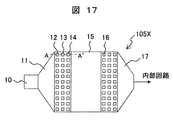
- FIG. 17 is a diagram illustrating a configuration of a protection circuit of an electronic device which is a comparative example with the present invention.
- 17 includes a pad 10 for connecting an external signal, a wiring layer 11 for connecting the pad 10 and the contacts 12, 13, and 14, and a contact 12 for connecting the wiring layer 11 and the protective resistor 15. , 13, 14, a protective resistor 15 that protects the internal circuit from surges and noises input from the pad 10, and a contact 16 and a wiring layer 17 that connect the protective resistor 15 to the internal circuit.
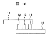
- FIG. 18 is a view showing a cross section A-A ′ of FIG. 17.
- the wiring layer 11 and the protective resistor 15 are formed in different layers.
- the wiring layer 11 formed in the upper layer and the protective resistor 15 formed in the lower layer are electrically connected by contacts 12, 13, and 14 formed across the layers.
- contacts 12, 13, and 14 formed across the layers.
- aluminum wiring is used for the wiring layer 11 and tungsten is used for the contacts 12, 13, and 14.
- polysilicon or silicide is often used for the protective resistor 15.
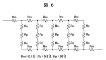
- FIG. 19 is a diagram showing an equivalent circuit of the contact portion of the protection circuit of FIG.
- the wiring layer 11 is represented by a resistance Rm, and a typical sheet resistance of 0.1 ⁇ / ⁇ of aluminum is used.
- the contacts 12, 13, and 14 are represented by a resistance Rc, and 0.3 ⁇ / ke is used as a resistance value.
- the protective resistor 15 is represented by a resistor Rp, and a typical sheet resistance of 20 ⁇ / ⁇ of polysilicon is used.
- FIG. 20 is a calculation result of the current of each contact of the protection circuit of the electronic device of FIG.
- the current I3 flowing through the contact 14 is the largest, most of the current flows through the contact 14, the currents I1 and I2 flowing through the contacts 12 and 13 are much smaller than the current I3, and the contacts 12 and 13 have almost no current. Does not flow. That is, the current flows through the contact 14 arranged on the center side of the protective resistor 15 in the direction in which the current flows, that is, the contact 16 connected to the internal circuit and the contact 14 closest to the wiring layer 17, and the contact away from the protective resistor 15. Almost no current flows through 12 and 13.
- This calculation result shows that only the contact 14 having the shortest length of the protective resistor 15 (protective resistor portion length) contributes to the allowable current value of the protective resistor 15 (hereinafter referred to as the allowable current). It is indicated that the contacts 12 and 13 whose part length (protective resistance part length) is longer than the contact 14 do not contribute to the allowable current.
- the resistance width of the protective resistor 15 is determined by the allowable loss and resistance value of the protective resistor 15.
- the allowable loss of the protective resistor 15 is generally determined by the resistance area.
- the resistance value of the protective resistor 15 is determined in circuit design.
- the size of the contact is determined by the manufacturing process. For these reasons, if the resistance width of the protective resistor 15 is determined at the time of circuit design, the number of contacts (contacts that can shorten the length of the protective resistor portion) that can contribute to the allowable current that can be arranged in the protective resistor 15 is determined.
- the allowable current of the resistor 15 is determined.
- the allowable current is determined. In other words, the allowable current is limited by the resistance width of the protective resistor 15. This means that when a surge voltage or the like is applied to the protection circuit, the contact breaks before the protection resistor 15 breaks, and the contact limits the allowable current of the protection circuit. This occurs not only on the wiring layer 11 side but also on the wiring layer 17 side.
- the present invention has been made in view of the above circumstances, and an object thereof is to provide an electronic device provided with a protective resistor having a large allowable current.
- an electronic device of the present invention includes: A protection circuit for protecting an internal circuit provided inside, a pad for electrically connecting an external signal, a protection resistor provided between the pad and the internal circuit, and a length of the protection resistor A first wiring layer arranged on one end side and electrically connected to the pad, and a first wiring layer arranged on the other end side in the length direction of the protective resistor and electrically connected to the internal circuit Two wiring layers; a plurality of first contacts that electrically connect the first wiring layer and the protective resistor; and a plurality of second contacts that electrically connect the second wiring layer and the protective resistor.
- the first wiring layer is disposed on one end side in the length direction of the protective resistance and extends to have a longitudinal direction along a width direction perpendicular to the length direction
- the second wiring layer is disposed on the other end side in the length direction of the protective resistor, and extends so as to have a longitudinal direction along the width direction
- the plurality of first contacts are arranged in a row along the longitudinal direction of the first wiring layer
- the plurality of second contacts are arranged in a row along the longitudinal direction of the second wiring layer
- the first wiring layer and the second wiring layer are disposed so as to face each other via the protective resistance
- the pad is electrically connected to one end in the longitudinal direction of the first wiring layer
- the internal circuit is electrically connected to an end of the second wiring layer opposite to an end opposite to one end to which the pad of the first wiring layer is connected.
- FIG. 3 is a diagram illustrating a configuration of a protection circuit of the electronic device according to the first embodiment.
- FIG. 3 is a diagram illustrating a configuration in which wiring layers 3 and 6 are removed from the protection circuit of the electronic device according to the first embodiment.
- FIG. 2 is a view showing a cross section A-A ′ of FIG. 1. It is a figure which shows the relationship between the sheet resistance of protection resistance, and resistance width.
- FIG. 3 is a diagram illustrating a configuration in which the arrangement of pads 1 of the protection circuit of the electronic device according to the first embodiment is changed.
- FIG. 3 is a diagram illustrating an equivalent circuit of a protection circuit of the electronic device according to the first embodiment. It is a figure which shows the structure of the protection circuit of the electronic device of Example 2.
- FIG. 6 is a diagram illustrating a configuration in which wiring layers 20 and 23 are removed from a protection circuit of an electronic device according to a second embodiment.
- FIG. 10 is a diagram illustrating a configuration of a protection circuit of an electronic device according to a third embodiment.
- FIG. 6 is a diagram illustrating a configuration in which wiring layers 25 and 32 are removed from a protection circuit of an electronic device according to a third embodiment.
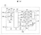
- FIG. 10 is a diagram illustrating a configuration of a protection circuit of an electronic device according to a fourth embodiment.
- FIG. 10 is a diagram illustrating a configuration in which wiring layers 37 and 41 are removed from a protection circuit of an electronic device according to a fourth embodiment.
- FIG. 10 is a diagram illustrating a configuration of a protection circuit of an electronic device according to a fifth embodiment.
- FIG. 10 is a diagram illustrating a configuration in which wiring layers 45 and 53 are removed from a protection circuit of an electronic device according to a fifth embodiment.
- FIG. 10 is a diagram illustrating a configuration of a protection circuit of an electronic device according to a sixth embodiment. It is a figure which shows the structure of the electronic device which concerns on one Example of this invention. It is a figure which shows the structure of the protection circuit of the electronic device which is a comparative example with this invention.
- FIG. 12 is a diagram showing a cross section taken along line A-A ′ of FIG. 11. It is a figure which shows the equivalent circuit of the contact part of the protection circuit of FIG. It is a calculation result of the electric current of each contact of the protection circuit of the electronic device of FIG.
- the present invention is not limited to the vehicle-mounted flow sensor device 100, and other pressure sensors and acceleration sensors.
- the present invention can be widely applied to the electronic device 100 including a sensor device that detects a physical quantity such as an angular velocity sensor.
- FIG. 16 is a diagram showing a configuration of an electronic device according to an embodiment of the present invention.
- the flow sensor device 100 includes an LSI 120, a sensor element 121, and a temperature sensor 122.
- the LSI 120 is connected to an external device through a power supply terminal 102a, a sensor output terminal 102b, and a ground terminal 103.
- the power supply terminal 102a and the sensor output terminal 102b correspond to pads of a protection circuit described later.
- the LSI 120 processes the signals acquired from the sensor element 121 and the temperature sensor 122 to generate a sensor output signal, and a protection circuit 105 (105a to 105d) that protects the internal circuit 104 from noise entering from outside.
- a protective circuit 105 a is provided between the power supply terminal 102 a and the internal circuit 104
- a protective circuit 105 b is provided between the sensor output terminal 102 b and the internal circuit 104
- protective circuits 105 c and 105 d are provided between the bonding pad 130 c and the internal circuit 104. Each is arranged.
- the protection circuit 105 (105a to 105d) includes a resistor 106 and a capacitor (capacitance element) 107.
- the resistor 106 is electrically connected in series between the pads (terminals) 102 a, 102 b, 130 c and the internal circuit 104.
- Capacitor 107 has one electrode electrically connected to the wiring between resistor 106 and internal circuit 104, and the other electrode electrically connected to the ground potential. Thereby, the wiring between the resistor 106 and the internal circuit 104 is electrically connected to the ground potential via the capacitor 107.
- the sensor element 121 includes a detection unit 123 and a bonding pad 130b, and is electrically connected by connecting the bonding pad 130b to the bonding pad 130a of the LSI 120 via the bonding wire 131.
- the temperature sensor 122 has a thermistor 124 and a bonding pad 130d, and is electrically connected by connecting the bonding pad 130d to the bonding pad 130c of the LSI 120 via the bonding wire 131.
- the above-described electronic apparatus 100 can be applied in common to each embodiment described below.
- FIG. 1 is a diagram illustrating a configuration of a protection circuit of the electronic device according to the first embodiment.
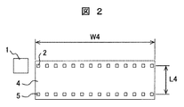
- FIG. 2 is a diagram illustrating a configuration in which the wiring layers 3 and 6 are removed from the protection circuit of the electronic device according to the first embodiment.
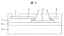
- FIG. 3 is a view showing a cross section taken along line AA ′ of FIG.
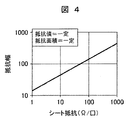
- FIG. 4 is a diagram illustrating the relationship between the sheet resistance and the resistance width of the protective resistance.
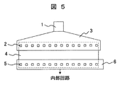
- FIG. 5 is a diagram illustrating a configuration in which the arrangement of the pads 1 of the protection circuit of the electronic device according to the first embodiment is changed.
- FIG. 6 is a diagram illustrating an equivalent circuit of the protection circuit of the electronic device according to the first embodiment.
- the protection circuit 105 ⁇ / b> A of the electronic device 100 of this embodiment includes a pad 1, a wiring layer (first wiring layer) 3, a contact (first contact) 2, a protective resistor 4, and a contact (second contact) 5. And a wiring layer (second wiring layer) 6.
- the pad 1 is a terminal portion for connecting an external signal to the protection circuit 105A.
- the wiring layer 3 is a wiring portion that connects the pad 1 and the contact 2.
- the contact 2 is a wiring portion that connects the wiring layer 3 and the protective resistor 4.
- the protective resistor 4 is a circuit component (circuit element) that protects the internal circuit from surges and noises input from the pad 1.
- the contact 5 and the wiring layer 6 are provided on the side opposite to the side where the contact 2 and the wiring layer 3 are provided with respect to the protective resistance 4 in the direction i (see FIG. 1) in which the current flows. Connect to the circuit.
- the wiring layers 3 and 6 and the protective resistor 4 are formed in different layers on the substrate.
- the wiring layers 3 and 6 are disposed in an upper layer with respect to the protective resistor 4, and the protective resistor 4 is disposed in a lower layer with respect to the wiring layers 3 and 6.
- the wiring layer 3 formed in the upper layer and the protective resistor 4 formed in the lower layer are electrically connected by the contact 2 formed between the layer in which the wiring layer 3 is formed and the layer in which the protective resistor 4 is formed.
- the wiring layer 6 formed in the upper layer and the protective resistor 4 formed in the lower layer are formed by the contact 5 formed between the layer in which the wiring layer 6 is formed and the layer in which the protective resistor 4 is formed. Electrically connected.
- the protective resistor 4 is disposed on the field oxide film 8 disposed on the silicon substrate 9, and the interlayer oxide film 7 is disposed on the upper portion.
- the withstand voltage of the protective resistor 4 (withstand voltage between the silicon substrate 9) can be improved and the surge and noise applied from the pad 1 can be prevented. High withstand pressure.
- Protective resistor 4 is required to have high allowable loss, high withstand voltage to ground, and high allowable current.
- the allowable loss of the protective resistor 4 is determined according to the area of the protective resistor 4, and the withstand voltage of the protective resistor 4 is determined by the thickness of the field oxide film 8. Further, the allowable current of the protective resistor 4 is determined by the width W4 (see FIG. 2) of the protective resistor 4 as described above.
- the width (W4) of the protective resistor 4 is increased while keeping the area (allowable loss) of the protective resistor 4 and the resistance value of the protective resistor 4 constant, the sheet resistance of the protective resistor 4 is increased as shown in FIG. This can be achieved.
- the sheet resistance of the protective resistor 4 is increased, and the resistance width W4 is increased with respect to the resistance length L4 (see FIG. 2), thereby increasing the number of contacts that can be arranged on both sides of the protective resistor 4.
- the widths W3 and W6 (see FIG. 1) of the wiring layers 3 and 6 are widened to prevent the allowable current from being limited by the influence of the wiring layers 3 and 6.
- the pad 1 is arranged on the left side of the protective resistor 4 in order to equalize the current flowing through the contacts 2 and 5.
- the surge current flowing from the pad 1 is concentrated in the central portion of the protective resistor 4 (the current path in the central portion is the shortest). The allowable loss and allowable current are reduced.
- a surge current can be made to flow relatively uniformly in all the contacts 2 and 5.
- the wiring layers 3 and 6 are formed in a shape having a longitudinal direction in the direction of the width W4 of the protective resistor 4, and the contacts 2 and 5 are dispersedly arranged along the direction of the width W4.
- one end 6A of the wiring layer 6 is located on one end 3A side of the wiring layer 3, and the other end 6B of the wiring layer 6 is located on the other end 3B side of the wiring layer 3.
- Two wiring layers 3 and 6 are arranged so as to be positioned.
- the two wiring layers 3 and 6 are arranged in parallel so that the longitudinal direction is along the directions of the widths W3 and W6.
- the pad 1 is electrically connected to one end 3A in the direction of the width W3 of the wiring layer 3 (same as the direction of the width W4).
- the end corresponding to the end 3B opposite to the end 3A side to which the pad 1 of the wiring layer 3 is connected in the wiring layer 6, in the direction of the width W6 of the wiring layer 6 (the same as the direction of the width W4), the end corresponding to the end 3B opposite to the end 3A side to which the pad 1 of the wiring layer 3 is connected.
- the part 6B side is electrically connected to the internal circuit. That is, the end 3A connected to the pad 1 in the wiring layer 3 and the end 6B connected to the internal circuit in the wiring layer 6 are located on the opposite side in the direction of the width W4 with respect to the protective resistance 4. Placed.
- FIG. 6 is a diagram illustrating an equivalent circuit of the protection circuit of the electronic device according to the first embodiment.
- the wiring layers 3 and 6 are represented by a resistance Rm, and a typical sheet resistance of 0.1 ⁇ / ⁇ of aluminum is used.
- the resistance of each contact 2 and 5 is represented by a resistance Rc, and 0.3 ⁇ / piece is used as the resistance value.
- the protective resistor 4 is represented by a resistor Rp, and a typical sheet resistance of 20 ⁇ / ⁇ of polysilicon is used.
- the total resistance of all the current paths is equal, and the current flows evenly in a direct current.
- This increases the sheet resistance of the protective resistor 4 and increases the resistance width W4 with respect to the resistance length L4, thereby increasing the approximation of the equivalent circuit shown in FIG. Current flows evenly. As a result, current concentration in a specific contact can be reduced, and a reduction in allowable current of the protection circuit 105A can be prevented.
- the contacts 2 and 5 are on the linear current path flowing from the pad 1 or on the linear current path flowing toward the internal circuit, and the wiring layer 3 is directed to the right in the drawing.
- the direction of the current is bent at the contact 2 so that the current flowing in the direction of the resistance width W3 flows in the protective resistor 4 in the downward direction of the drawing (direction of the resistance length L4).
- the resistance temperature coefficient is also increased, so that the current dispersion effect due to current heat generation is also increased, current concentration can be reduced, and the allowable current can be prevented from being lowered.
- the contacts 2 and 5 disposed in the wiring layers 3 and 6 are in the longitudinal direction of the wiring layers 3 and 6 (directions of widths W3, W4, and W6). Are lined up in a row. Thereby, the resistance lengths of the protective resistors 4 connected to the contacts 2 and 5 can be made equal, and the resistance values of the protective resistors 4 connected to the contacts 2 and 5 can be made uniform.
- the sheet resistance of the protective resistor 4 is increased, and the resistance width W4 is increased with respect to the resistance length L4, thereby increasing the number of contacts that can be arranged on both sides of the protective resistor 4 and the allowable current. Can be increased. Further, by making the direction of the current flowing through the wiring layers 3 and 6 different from the direction of the current flowing through the protective resistor 4, when the current flowing through the wiring layer 3 changes the direction of the current at the contact 2, Since the current bending can be made uniform, the current concentration at a specific contact can be reduced and the allowable current can be prevented from lowering.
- the pitch of the contacts 2 and 5 is set to be three times or more the size of the contacts 2 and 5.
- the contact is made of tungsten, and since the metal has a high resistivity, the heat generated by the current is large. Tungsten is a hard metal with a high Young's modulus. For this reason, when a large number of contacts 2 and 5 are arranged with the minimum dimensions as in the conventional example, the contacts 2 and 5 are easily broken by the heat generated by the surge current and the stress due to the thermal expansion of tungsten itself.
- the number of contacts 2 and 5 is made one and the distance between the contacts is widened to prevent a large thermal stress from being generated. This suppresses a decrease in the allowable current of the contacts 2 and 5 so that a large allowable current can be obtained in the protection circuit 105A.
- the resistance width W4 is wide and the resistance length L4 is short, the distance from the contact 2 to the contact 5 of the protective resistance 4 is short, and a wide wiring layer 3, 6 is connected to the contacts 2, 5. ing. For this reason, the heat generated from the protective resistor 4 is not only radiated to the silicon substrate 9 via the field oxide film 8, but also the heat radiated from the contacts 2 and 5 via the wiring layers 3 and 6 is increased. As a result, the allowable loss of the protective resistor 4 can be increased.
- FIG. 7 is a diagram illustrating a configuration of the protection circuit of the electronic device according to the second embodiment.
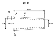
- FIG. 8 is a diagram illustrating a configuration in which the wiring layers 20 and 23 are removed from the protection circuit of the electronic device according to the second embodiment.
- the protection circuit 105B of the electronic device 100 includes a pad 18, a wiring layer (first wiring layer) 20, a contact (first contact) 19, a protective resistor 21, a contact (second contact) 22, and the like. And a wiring layer (second wiring layer) 23.
- the pad 18 is a terminal portion for connecting an external signal to the protection circuit 105B.
- the wiring layer 20 is a wiring portion that connects the pad 18 and the contact 19.
- the contact 19 is a wiring portion that connects the wiring layer 20 and the protective resistor 21.
- the protective resistor 21 is a circuit component (circuit element) that protects the internal circuit from surges and noises input from the pad 18.
- the contact 22 and the wiring layer 23 are provided on the opposite side of the protective resistor 21 from the side on which the contact 19 and the wiring layer 20 are provided in the direction i (see FIG. 7) in which the current flows. Connect to the circuit.
- This embodiment is basically the same as the first embodiment, but the shape of the protective resistor 21 is such that the resistance length L4A on the pad 18 side is larger than the resistance length L4B on the opposite side. That is, the protective resistor 21 has a length dimension L4A in the length direction on one end portion side to which the pad 18 in the wiring layer 20 is connected, in the length direction on the other end portion side of the wiring layer 20. It is larger than the dimension L4B.
- the wiring layer 20 and the wiring layer 23 are arranged in a non-parallel state (tilted state) along the width direction W21 of the protective resistor 21.
- the wiring layer 20 and the wiring layer 23 are not parallel, the two wiring layers 20 and 23 are arranged so that the longitudinal direction thereof is along the direction of the width W 21 of the protective resistor 21.
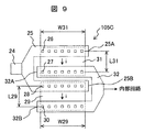
- FIG. 9 is a diagram illustrating the configuration of the protection circuit of the electronic device according to the third embodiment.
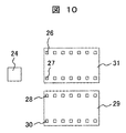
- FIG. 10 is a diagram illustrating a configuration in which the wiring layers 25 and 32 are removed from the protection circuit of the electronic device according to the third embodiment.
- the protection circuit 105C of the electronic device 100 includes the pad 24, the wiring layers 25 and 32, the contacts 26, 17, 18, and 30 and the protection resistors 29 and 31.
- the wiring layer (first wiring layer) 25 extends along the direction of the width W29 of the protective resistance 29 and the first wiring portion 25A extending along the width W31 of the protective resistance 31.
- the first wiring part 25A and the second wiring part 25B form a comb-tooth structure.
- the wiring layer (second wiring layer) 32 includes a first wiring portion 32A extending along the width W31 of the protective resistor 31 and a second wiring extending along the width W29 of the protective resistor 29.
- the first wiring part 32A and the second wiring part 32B have a comb-tooth structure.
- the pad 24 is a terminal portion for connecting an external signal to the protection circuit 105C.
- the wiring layer 25 composed of the first wiring portion 25A and the second wiring portion 25B is a wiring portion that connects the pad 24 and the contacts (first contacts) 26, 28.
- the contact 26 is a wiring part that connects the wiring layer 25 and the protective resistor 31, and is provided in the first wiring part 25 ⁇ / b> A.
- the contact 28 is a wiring portion that connects the wiring layer 25 and the protective resistor 29 and is provided in the second wiring portion 25B.
- the protective resistors 29 and 31 are circuit components (circuit elements) that protect internal circuits from surges and noises input from the pad 24.
- the contact (second contact) 27 and the first wiring portion 32A of the wiring layer 32 are connected to the protective resistor 31 in the direction i of current flow or the direction of the resistance length L29 (see FIG. 9).
- 25 is provided on the side opposite to the side where the first wiring portion 25A is provided, and the protective resistor 31 is connected to the internal circuit.
- the contact (second contact) 30 and the second wiring portion 32B of the wiring layer 32 are arranged such that the contact 28 and the wiring with respect to the protective resistor 29 in the direction i of current flow or the direction of the resistance length L29 (see FIG. 9).
- the layer 25 is provided on the side opposite to the side where the second wiring portion 25B is provided, and connects the protective resistor 29 to the internal circuit.
- the wiring layer 25 and the wiring layer 32 are arranged between the first wiring parts 25A and 32A and the second wiring parts 25B and 32B in one wiring layer formed in a comb-teeth shape. It arrange
- this embodiment is basically the same as the first embodiment, two protection resistors 29 and 31 are provided, and the wiring layers 25 and 32 provided for each protection resistor have a comb-tooth structure.
- the resistance widths W29 and W31 of the protective resistors 29 and 31 can be shortened to 1 ⁇ 2 that of the first embodiment.
- the influence of the inductance of the wiring layer 25 is reduced and each contact is reduced.
- the flowing current can be more equalized. Thereby, equalization of the current flowing from the pad 24 to each contact can be realized, and a reduction in allowable current can be prevented.
- the resistance length L29 of the protection resistor 29 and the resistance length L31 of the protection resistor 31 are set to be the same length so that the resistance value of the protection resistor 29 and the resistance value of the protection resistor 31 are equal.
- the resistance length L29 of the protection resistor 29 and the resistance length L31 of the protection resistor 31 are made different from each other to thereby change the resistance value of the protection resistor 29 and the protection resistance.
- the resistance value of the resistor 31 may be equal.
- the first wiring portion 25A of the wiring layer 25 and the first wiring portion 32A of the wiring layer 32 do not need to be parallel, and may be inclined as in the second embodiment.
- the second wiring part 25B of the wiring layer 25 and the second wiring part 32B of the wiring layer 32 do not need to be parallel, and may be arranged inclined as in the second embodiment.
- the number of wiring portions 25A and 25B in the wiring layer 25 and the number of wiring portions 32A and 32B in the wiring layer 32 may be three or more.
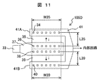
- FIG. 11 is a diagram illustrating the configuration of the protection circuit of the electronic device according to the fourth embodiment.
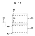
- FIG. 12 is a diagram illustrating a configuration in which the wiring layers 37 and 41 are removed from the protection circuit of the electronic device according to the fourth embodiment.
- the protection circuit 105D of the electronic device 100 includes the pad 33, the wiring layers 37 and 41, the contacts 34, 36, 38, and 40, and the protection resistors 35 and 39.
- the wiring layer (first wiring layer) 37 is extended along the widths W35 and W39 of the protective resistors 35 and 39.
- the wiring layer (second wiring layer) 41 includes a first wiring portion 41A extending along the width W35 of the protective resistor 35 and a second wiring extending along the width W39 of the protective resistor 39.
- the first wiring portion 41A and the second wiring portion 42B form a comb-tooth structure.
- the wiring layer 37 is disposed between the comb teeth formed by the first wiring part 41A and the second wiring part 42B.
- the pad 24 is a terminal part for connecting an external signal to the protection circuit 105D.
- the wiring layer 37 is a wiring portion that connects the pad 33 and the contacts (first contacts) 36 and 38.
- the contact 36 is a wiring portion that connects the wiring layer 37 and the protective resistor 35.
- the contact 38 is a wiring portion that connects the wiring layer 27 and the protective resistor 39.
- the protective resistors 35 and 39 are circuit components (circuit elements) that protect the internal circuit from surges and noises input from the pad 33.
- the contact (second contact) 34 and the first wiring portion 41A of the wiring layer 41 are configured such that the contact 36 and the wiring layer with respect to the protective resistor 35 in the direction i of current flow or the direction of the resistance length L35 (see FIG. 11).
- the contact (second contact) 40 and the second wiring portion 41B of the wiring layer 41 are connected to the protection resistor 39 in the direction i of current flow or the direction of the resistance length L39 (see FIG. 11).
- the protective resistor 39 is provided on the side opposite to the side where the layer 25 is provided, and connects the protective resistor 39 to the internal circuit.
- contacts 36 connected to the protective resistor 35 and contacts 38 connected to the protective resistor 39 are arranged in a line along the longitudinal direction of the wiring layer 37.
- the wiring layer 37 is disposed so as to be interposed between the first wiring part 41A and the second wiring part 41B of the wiring layer 41 formed in a comb-teeth shape.
- this embodiment is basically the same as the first embodiment, two protection resistors 35 and 39 are provided, and the wiring layer 41 provided for each protection resistor has a comb-tooth structure.
- the resistance widths W35 and W39 of the protective resistors 35 and 39 can be shortened to 1 ⁇ 2 that of the first embodiment.
- the influence of the inductance of the wiring layer 37 is reduced and each contact is reduced.
- the flowing current can be more equalized. Thereby, equalization of the current flowing from the pad 33 to each contact can be realized, and a reduction in allowable current can be prevented.
- the protective resistors 35 and 39 are arranged on both sides of the wiring layer 37, so that the mounting efficiency of the protective resistors can be improved as compared with the protective circuit 105C of the third embodiment, and the chip size is smaller. Can be realized.
- the wiring layer 41 connected to the internal circuit is configured in a comb-tooth shape, but the wiring layer 37 connected to the pad 33 is configured in a comb-tooth shape, and the wiring layer 41 is configured in a comb-tooth shape.
- the wiring layer 37 may be disposed between two wiring portions.
- the resistance length L35 of the protection resistor 35 and the resistance length L39 of the protection resistor 31 are made the same length so that the resistance value of the protection resistor 35 and the resistance value of the protection resistor 39 are equal.
- the resistance length L35 of the protective resistor 35 and the resistance length L39 of the protective resistor 39 are made different from each other, whereby the resistance value of the protective resistor 35 and the protection resistance 35 are protected.
- the resistance value of the resistor 35 may be equal.
- the wiring layer 37 and the first wiring portion 41A of the wiring layer 41 do not need to be parallel, and may be arranged inclined as in the second embodiment. Further, the wiring layer 37 and the second wiring portion 41B of the wiring layer 41 do not need to be parallel, and may be arranged inclined as in the second embodiment.
- the wiring layer 37 may have a shape in which the width dimension in the direction perpendicular to the longitudinal direction changes along the longitudinal direction.
- FIG. 13 is a diagram illustrating the configuration of the protection circuit of the electronic device according to the fifth embodiment.
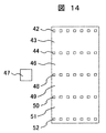
- FIG. 14 is a diagram illustrating a configuration in which the wiring layers 45 and 53 are removed from the protection circuit of the electronic device according to the fifth embodiment.
- the protection circuit 105E of the electronic device 100 includes a pad 47, wiring layers 45 and 53, contacts 42, 44, 48, 50, and 52, and protection resistors 43, 46, 49, and 51. Composed.
- the wiring layer (first wiring layer) 45 has a first wiring portion 45A and a second wiring portion 45B extending along the direction of the width We of the protective resistors 43, 46, 49, 51.
- the first wiring portion 45A and the second wiring portion 45B form a comb-tooth structure.
- the wiring layer (second wiring layer) 53 includes a first wiring portion 53A, a second wiring portion 53B, and a third wiring portion 53C that extend along the direction of the width We of the protective resistors 43, 46, 49, 51.
- the first wiring part 32A, the second wiring part 32B, and the third wiring part 53C form a comb-tooth structure.
- the pad 47 is a terminal part for connecting an external signal to the protection circuit 105C.
- the wiring layer 45 is a wiring portion that connects the pad 47 and the contacts (first contacts) 44 and 50.
- the contact 44 is a wiring portion that connects the wiring layer 45 and the protective resistors 43 and 46, and is provided in the first wiring portion 45A.
- the contact 50 is a wiring portion that connects the wiring layer 45 and the protective resistors 49 and 51, and is provided in the second wiring portion 25B.
- the protective resistors 43, 46, 49, 51 are circuit components (circuit elements) that protect the internal circuit from surges and noises input from the pad 47.
- the contact (second contact) 42 and the first wiring portion 53A of the wiring layer 53 are connected to the protective resistor 43 in the direction i of current flow or the direction of the resistance length L43 (see FIG. 13).
- 45 is provided on the side opposite to the side where the first wiring portion 45A is provided, and connects the protective resistor 43 to the internal circuit.
- the contact (second contact) 48 and the second wiring portion 53B of the wiring layer 53 are configured such that the contact 44 and the wiring layer with respect to the protective resistance 46 in the direction i of current flow or the direction of the resistance length L46 (see FIG. 13).
- 45 is provided on the side opposite to the side where the first wiring portion 45A is provided, and connects the protective resistor 46 to the internal circuit.
- the contact 48 and the second wiring portion 53B of the wiring layer 53 are connected to the protective resistor 49 in the direction i of the current flow or the resistance length L49 (see FIG. 13).
- the protective resistor 49 is connected to the internal circuit.
- the contact (second contact) 52 and the third wiring portion 53C of the wiring layer 53 are connected to the contact 50 and the wiring layer with respect to the protective resistor 51 in the direction i of current flow or the direction of the resistance length L51 (see FIG. 13).
- 45 is provided on the side opposite to the side where the second wiring portion 45B is provided, and connects the protective resistor 51 to the internal circuit.
- the wiring layer 45 and the wiring layer 53 are arranged so that each wiring part in the other wiring layer is interposed between each wiring part in one wiring layer formed in a comb-teeth shape.
- this embodiment is basically the same as the first embodiment, four protection resistors 43, 46, 49, 51 are provided, and the wiring layers 45, 53 provided for each protection resistor have a comb-tooth structure. .
- the resistance widths W43, W46, W49, and W51 of the protective resistors 43, 46, 49, and 51 can be shortened to 1 ⁇ 4 that of the first embodiment.
- the inductance of the wiring layer 45 can be reduced. The influence can be reduced, and the current flowing through each contact can be made more uniform. Thereby, equalization of the current flowing through each contact can be realized, and a reduction in allowable current can be prevented.
- the wiring layer 45 or the wiring layer 53 is formed in a comb-tooth shape, and the wiring portion of the other wiring layer is disposed between the two wiring portions of one wiring layer forming the comb-tooth shape. Then, protective resistors are arranged on both sides of the wiring portion of the other wiring layer.
- the protective resistors 43, 46, 49, 51 are integrally formed, and there is no need to provide a gap between the protective resistors 43, 46, 49, 51, so that the mounting efficiency can be improved. A small chip size can be realized.
- the first wiring portion 45A of the wiring layer 45 and the first wiring portion 53A and the second wiring portion 53B of the wiring layer 53 do not have to be parallel, and are arranged inclined as in the second embodiment. May be. Further, the second wiring portion 45B of the wiring layer 45 and the second wiring portion 53B and the third wiring portion 53C of the wiring layer 53 do not have to be parallel, and may be inclined as in the second embodiment. .
- the number of wiring portions 45A and 45B in the wiring layer 45 may be three or more, and the number of wiring portions 53A, 53B, and 53C in the wiring layer 53 may be four or more.
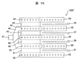
- FIG. 15 is a diagram illustrating the configuration of the protection circuit of the electronic device according to the sixth embodiment.
- the protection circuit 105F of the electronic device 100 of this embodiment is basically the same as that of the fifth embodiment.
- This embodiment is different from the fifth embodiment in that the MOS transistor is arranged at the exit of the protective resistors 43, 46, 49, 51.
- the MOS transistor includes a drain electrode connected to the wiring layers (second wiring layers) 54, 58, 62, gate electrodes 55, 57, 59, 61, and source electrodes connected to the wiring layers 56, 60.
- the Each drain electrode of the MOS transistor is connected to protective resistors 43, 46, 49, 51 via wiring layers 54, 58, 62, respectively.
- the protective resistance and the MOS transistor wiring can be easily arranged by arranging the protective resistance connected to the comb-shaped wiring layer and the comb-shaped MOS transistor side by side.
- the mounting efficiency of the protection circuit 105F can be improved, and a smaller chip size can be realized.
- the wiring of the protective resistor and the MOS transistor can be further facilitated.
- the mounting efficiency of the protection circuit 105F can be further improved, and a smaller chip size can be realized.
- the MOS transistor when a surge voltage is applied to the pad 47, the MOS transistor causes a snapback phenomenon. The current is concentrated on the MOS transistor in which the snapback phenomenon occurs, and the MOS transistor is destroyed.
- the protective resistors 43, 46, 49, 51 are connected to each transistor, current concentration on the snap-back MOS transistor can be suppressed, and a higher allowable current can be realized. it can.
- the allowable current of the protective resistor can be increased, and the protective resistor can be reduced in resistance.
- the voltage applied to the pad when a surge voltage is applied can be reduced. Therefore, a protection circuit with a low substrate breakdown voltage in an electronic device using a fine process can be used effectively.
- this invention is not limited to each above-mentioned Example, Various modifications are included.
- the above-described embodiments have been described in detail for easy understanding of the present invention, and are not necessarily limited to those having all the configurations.
- a part of the configuration of one embodiment can be replaced with the configuration of another embodiment, and the configuration of another embodiment can be added to the configuration of one embodiment.
- Protection Resistance 50 Contact (first contact) 51 Protection resistance 52 Contact (second contact) 53 Wiring layer (second wiring layer) 54 Wiring layer (second wiring layer) 55 , Gate electrode, 58... Wiring layer (second wiring layer), 59... Gate electrode, 60... Wiring layer (third wiring layer), 61. Electrode, 62 ... wiring layer (second wiring layer), 100 ... electronic device, 105A to 105F ... protection circuit.
Landscapes
- Semiconductor Integrated Circuits (AREA)
Abstract
本発明の目的は許容電流の大きい保護抵抗を備えた電子装置を提供することにある。 第1配線層3及び第2配線層6は保護抵抗4の長さ方向の両端部に対向するように配置され、幅方向W3,W4に沿って長手方向を有するように延設される。第1コンタクト2及び第2コンタクト5は第1配線層3及び第2配線層6に長手方向に沿って列を成すように配置される。パッド1は第1配線層3の長手方向における一方の端部に電気的に接続され、内部回路は第1配線層3のパッド1が接続される一方の端部とは反対側の端部に対向する第2配線層6の端部に電気的に接続される。
Description
本発明は、フィールド酸化膜上に配置された保護抵抗と保護抵抗の両側にコンタクトを介して接続される配線層とを備えた電子装置に関する。
電子装置の従来例には国際公開WO2013/018134号公報(特許文献1)に記載されたセンサ装置などがある。特許文献1のセンサ装置は、外部装置が接続される外部端子と、グラウンドに接地される接地端子と、センサ出力信号を生成する内部回路と、外部端子と内部回路との間に設けた抵抗素子及び容量素子とからなる保護回路とを有する(要約参照)。このセンサ装置は、抵抗素子を例えば金属シリサイドを用いて形成し、抵抗素子及び容量素子を電気的に接続する配線は例えばアルミニウム(Al)を用いて形成している。そして配線と抵抗素子及び容量素子との接続部においては、複数のコンタクトを設けて伝的な接続を確保している(段落0038参照)。
特許文献1に記載されている従来技術では、配線(以下、配線層という)と抵抗素子(以下、保護抵抗という)を接続するコンタクトの許容電流に対する配慮が欠けていた。
電子装置では、パッドに印加されるサージ電圧を基板耐圧以下にする必要がある。この為には電子装置の保護抵抗を低抵抗化してサージ電圧が印加された時にパッドに印加される電圧を低下させる必要がある。微細プロセスを用いた電子装置の保護回路における基板耐圧は低く、保護抵抗の低抵抗化がより強く求められる。しかし、従来の電子装置の保護回路に使用される保護抵抗は、保護抵抗の許容電流が小さく、保護抵抗を低抵抗化することが困難であった。
保護抵抗の許容電流が小さい理由について、図17~図20を参照して説明する。
電子装置の保護回路の構成について、図17を参照して説明する。図17は、本発明との比較例である電子装置の保護回路の構成を示す図である。
図17の電子装置の保護回路105Xは外部信号を接続するパッド10と、パッド10とコンタクト12,13,14とを接続する配線層11と、配線層11と保護抵抗15とを接続するコンタクト12,13,14と、パッド10から入力されるサージやノイズから内部回路を保護する保護抵抗15と、保護抵抗15を内部回路へ接続するコンタクト16および配線層17とから構成される。
配線層11と保護抵抗15との接続構造を、図18を参照して説明する。図18は、図17のA-A’断面を示す図である。
配線層11と保護抵抗15とは異なる層に形成されている。上層に形成された配線層11と下層に形成された保護抵抗15とは層間に跨って形成されたコンタクト12,13,14により電気的に接続される。配線層11にはアルミ配線が、コンタクト12,13,14にはタングステンが使用されることが、現在は一般的である。また、保護抵抗15にはポリシリコンやシリサイドが使われることが多い。
次に、図17の保護回路におけるコンタクト部分の等価回路を、図19を参照して説明する。図19は、図17の保護回路のコンタクト部分の等価回路を示す図である。
図19では、配線層11は抵抗Rmで表し、アルミの代表的なシート抵抗0.1Ω/□を用いた。コンタクト12,13,14は抵抗Rcで表し、抵抗値として0.3Ω/ケを用いた。また、保護抵抗15は抵抗Rpで表し、ポリシリコンの代表的なシート抵抗20Ω/□を用いた。
図19の等価回路を用いてコンタクト12,13,14に流れる電流I1,I2,I3を計算した。計算結果を図20に示す。図20は、図11の電子装置の保護回路の各コンタクトの電流の計算結果である。
この結果、コンタクト14に流れる電流I3が最も大きく、コンタクト14にほとんどの電流が流れ、コンタクト12,13に流れる電流I1,I2は電流I3に比べて非常に小さく、コンタクト12,13にはほとんど電流が流れない。つまり、電流が流れる方向において保護抵抗15の中央側に配置されるコンタクト14、すなわち内部回路に接続されるコンタクト16および配線層17に最も近いコンタクト14に電流が流れ、保護抵抗15から離れたコンタクト12,13にはほとんど電流が流れない。
この計算結果は、保護抵抗15の部分の長さ(保護抵抗部分長さ)が最も短くなるコンタクト14のみが保護抵抗15の許容電流値(以下、許容電流という)に貢献し、保護抵抗15の部分の長さ(保護抵抗部分長さ)がコンタクト14よりも長くなるコンタクト12,13は許容電流に貢献しないことを示す。
ここで、コンタクト1個当たりに流せる電流には限界があり、コンタクト1個当たりの許容電流値(以下、許容電流という)が決まっている。また、保護抵抗15の抵抗幅は保護抵抗15の許容損失と抵抗値とで決まる。保護抵抗15の許容損失は抵抗面積で概ね決まる。また保護抵抗15の抵抗値は回路設計上決定される。また、コンタクトのサイズは製造プロセスから決まっている。これらのことから、回路設計時に保護抵抗15の抵抗幅が決まれば、保護抵抗15に配置できる許容電流に貢献できるコンタクト(保護抵抗部分長さを短くできるコンタクト)の数が決まり、この結果、保護抵抗15の許容電流が決まる。
つまり、保護抵抗15の抵抗幅が決まれば、許容電流が決まる。言い換えれば、保護抵抗15の抵抗幅によって許容電流が制限される。このことは、保護回路にサージ電圧などを印加した場合に、保護抵抗15が破壊する前にコンタクトが破壊し、コンタクトが保護回路の許容電流を制限してしまうことを意味する。このことは配線層11側だけでは無く、配線層17側でも生じる。
本発明は上記事情に鑑みてなされたものであり、その目的は許容電流の大きい保護抵抗を備えた電子装置を提供することにある。
上記目的を達成するために、本発明の電子装置は、
内部に設けられた内部回路を保護する保護回路に、外部信号を電気的に接続するパッドと、前記パッドと前記内部回路との間に設けられた保護抵抗と、前記保護抵抗の長さ方向における一方の端部側に配置され前記パッドに電気的に接続された第1配線層と、前記保護抵抗の長さ方向における他方の端部側に配置され前記内部回路に電気的に接続された第2配線層と、前記第1配線層と前記保護抵抗とを電気的に接続する複数の第1コンタクトと、前記第2配線層と前記保護抵抗とを電気的に接続する複数の第2コンタクトと、を備えた電子装置において、
前記第1配線層は、前記保護抵抗の長さ方向の一方の端部側に配置されて、前記長さ方向に垂直な幅方向に沿って長手方向を有するように延設され、
前記第2配線層は、前記保護抵抗の前記長さ方向の他方の端部側に配置されて、前記幅方向に沿って長手方向を有するように延設され、
前記複数の第1コンタクトは前記第1配線層の前記長手方向に沿って列を成すように配置され、
前記複数の第2コンタクトは前記第2配線層の前記長手方向に沿って列を成すように配置され、
前記第1配線層と前記第2配線層とは前記保護抵抗を介して対向するように配置され、
前記パッドは前記第1配線層の前記長手方向における一方の端部に電気的に接続され、
前記内部回路は前記第1配線層の前記パッドが接続される一方の端部とは反対側の端部に対向する前記第2配線層の端部に電気的に接続される。
本発明によれば、配線層と保護抵抗とを電気的に接続するコンタクトの許容電流を大きくすることができ、許容電流の高い保護抵抗を備えた電子装置を提供することができる。上記した以外の課題、構成及び効果は、以下の実施形態の説明により明らかにされる。
以下、本発明の実施の形態について、図面を参照して説明する。
以下では、電子装置の一実施例として、車載向けフローセンサ装置100に適用した例を説明するが、本発明は車載向けフローセンサ装置100に限定されるものではなく、他の圧力センサ、加速度センサ或いは角速度センサ等の物理量を検出するセンサ装置を含む電子装置100に広く適用することができる。
本実施例に係るフローセンサ装置100を、図16を用いて説明する。図16は、本発明の一実施例に係る電子装置の構成を示す図である。
フローセンサ装置100は、LSI120とセンサ素子121と温度センサ122とにより構成される。LSI120は電源端子102aとセンサ出力端子102bと接地端子103とにより外部の装置と接続する。電源端子102a及びセンサ出力端子102bは、後述する保護回路のパッドに相当する。
また、LSI120はセンサ素子121及び温度センサ122から取得した信号を処理しセンサ出力信号を生成する内部回路104と、外部から侵入するノイズから内部回路104を保護する保護回路105(105a~105d)とを有する。電源端子102aと内部回路104との間に保護回路105aが、センサ出力端子102bと内部回路104との間に保護回路105bが、ボンディングパッド130cと内部回路104との間に保護回路105c,105dがそれぞれ配置される。
保護回路105(105a~105d)は、抵抗106とコンデンサ(容量素子)107とを有する。抵抗106は、パッド(端子)102a,102b,130cと内部回路104との間に電気的に直列接続される。コンデンサ107は、一方の電極が抵抗106と内部回路104との間の配線に電気的に接続され、他方の電極が接地電位に電気的に接続される。これにより、抵抗106と内部回路104との間の配線はコンデンサ107を介して接地電位に電気的に接続される。
センサ素子121は検出部123とボンディングパッド130bとを有し、ボンディングパッド130bからボンディングワイヤ131を介してLSI120のボンディングパッド130aに接続することで電気的に接続される。
温度センサ122はサーミスタ124とボンディングパッド130dとを有し、ボンディングパッド130dからボンディングワイヤ131を介してLSI120のボンディングパッド130cに接続することで電気的に接続される。
上述した電子装置100は、以下で説明する各実施例に共通して適用可能である。
次に、本発明に係る電子装置100の保護回路について説明する。
[実施例1]
本発明の第1の実施例である電子装置について、図1~図6を参照して説明する。図1は、実施例1の電子装置の保護回路の構成を示す図である。図2は、実施例1の電子装置の保護回路から配線層3,6を取り除いた構成を示す図である。図3は、図1のA-A’断面を示す図である。図4は、保護抵抗のシート抵抗と抵抗幅の関係を示す図である。図5は、実施例1の電子装置の保護回路のパッド1の配置を変更した構成を示す図である。図6は、実施例1の電子装置の保護回路の等価回路を示す図である。
本発明の第1の実施例である電子装置について、図1~図6を参照して説明する。図1は、実施例1の電子装置の保護回路の構成を示す図である。図2は、実施例1の電子装置の保護回路から配線層3,6を取り除いた構成を示す図である。図3は、図1のA-A’断面を示す図である。図4は、保護抵抗のシート抵抗と抵抗幅の関係を示す図である。図5は、実施例1の電子装置の保護回路のパッド1の配置を変更した構成を示す図である。図6は、実施例1の電子装置の保護回路の等価回路を示す図である。
本実施例の電子装置100の保護回路105Aは、パッド1と、配線層(第1配線層)3と、コンタクト(第1コンタクト)2と、保護抵抗4と、コンタクト(第2コンタクト)5と、配線層(第2配線層)6と、を備えて構成される。パッド1は保護回路105Aに外部信号を接続する端子部である。配線層3はパッド1とコンタクト2とを接続する配線部である。コンタクト2は配線層3と保護抵抗4とを接続する配線部である。保護抵抗4はパッド1から入力されるサージやノイズから内部回路を保護する回路部品(回路素子)である。コンタクト5及び配線層6は、電流が流れる方向i(図1参照)において、保護抵抗4に対してコンタクト2及び配線層3が設けられた側とは反対側に設けられ、保護抵抗4を内部回路へ接続する。
なお、配線層3,6と保護抵抗4とは基板上の異なる層に形成されている。配線層3,6は保護抵抗4に対して上層に、保護抵抗4は配線層3,6に対して下層に配置されている。上層に形成された配線層3と下層に形成された保護抵抗4とは、配線層3が形成された層と保護抵抗4が形成された層との間に跨って形成されたコンタクト2により電気的に接続される。また上層に形成された配線層6と下層に形成された保護抵抗4とは、配線層6が形成された層と保護抵抗4が形成された層との間に跨って形成されたコンタクト5により電気的に接続される。
また、保護抵抗4はシリコン基板9に配置されたフィールド酸化膜8の上に配置され、上部には層間酸化膜7が配置される。保護抵抗4をフィールド酸化膜8の上に配置することで、保護抵抗4の対地耐圧(シリコン基板9との間の耐圧)を向上させることができ、パッド1から印加されるサージやノイズに対して高い耐圧を持たせることができる。
保護抵抗4には高い許容損失、高い対地耐圧、高い許容電流が要求される。保護抵抗4の許容損失は保護抵抗4の面積に応じて決まり、保護抵抗4の対地耐圧はフィールド酸化膜8の厚さで決まる。また、保護抵抗4の許容電流は先述した様に保護抵抗4の幅W4(図2参照)で決まる。ここで、保護抵抗4の面積(許容損失)と保護抵抗4の抵抗値を一定にして保護抵抗4の幅W4を増加させようとすると、図4に示す様に保護抵抗4のシート抵抗を高くすることで実現できる。つまり、本実施例では保護抵抗4のシート抵抗を高くして、抵抗長L4(図2参照)に対して抵抗幅W4を長くすることで、保護抵抗4の両側に配置できるコンタクト数を増加させて、許容電流を増加させる。また、配線層3,6の幅W3,W6(図1参照)も広げ配線層3,6の影響で許容電流が制限されることを防ぐ。
また、各コンタクト2,5に流れる電流を均等化する為、パッド1を保護抵抗4の左側に配置する。図5に示す様にパッド1を保護抵抗4の上側に配置した場合、パッド1から流れるサージ電流は保護抵抗4の中央部に集中し(中央部の電流経路が最も短い)、保護抵抗4の許容損失および許容電流は低下する。これに対して、図1に示すようにパッド1を保護抵抗4の左側に配置することで、全てのコンタクト2,5に比較的均等に分散させてサージ電流を流すことができる。
すなわち本実施例では、配線層3,6は保護抵抗4の幅W4の方向に長手方向を有する形状に形成され、幅W4の方向に沿ってコンタクト2,5を分散配置する。この場合、配線層3の一方の端部3Aの側に配線層6の一方の端部6Aが位置し、配線層3の他方の端部3Bの側に配線層6の他方の端部6Bが位置するように、二つの配線層3,6が配置される。なお本実施例では、二つの配線層3,6は長手方向が幅W3,W6の方向に沿うように平行に配置されている。
そしてパッド1は配線層3の幅W3の方向(幅W4の方向に同じ)の一方の端部3Aに電気的に接続される。一方配線層6では、配線層6の幅W6の方向(幅W4の方向に同じ)において、配線層3のパッド1が接続される端部3A側とは反対側の端部3Bに対応する端部6Bの側が、内部回路に電気的に接続される。すなわち、配線層3におけるパッド1に接続される端部3Aと配線層6における内部回路に接続される端部6Bとは、保護抵抗4に対して幅W4の方向において反対側に位置するように、配置される。
次に、本実施例の保護回路105Aの作用効果について、図6を参照して説明する。図6は、実施例1の電子装置の保護回路の等価回路を示す図である。
図6では配線層3,6を抵抗Rmで表し、アルミの代表的なシート抵抗0.1Ω/□を用いる。各コンタクト2,5の抵抗は抵抗Rcで表し、抵抗値として0.3Ω/ケを用いる。また、保護抵抗4は抵抗Rpで表し、ポリシリコンの代表的なシート抵抗20Ω/□を用いる。この等価回路では全ての電流経路の合計抵抗は等しく、直流的には均等に電流が流れる。このことは、保護抵抗4のシート抵抗を高くし、抵抗長L4に対して抵抗幅W4を長くすることで図6に示した等価回路の近似性が高くなるので、より各コンタクト2,5に均等に電流が流れる。これらのことにより特定のコンタクトにおける電流集中を低減し、保護回路105Aの許容電流の低下を防ぐことができる。
また、サージ電流に関しても、全てのコンタクト2,5がパッド1から流れる直線状の電流経路上、又は内部回路に向かって流れる直線状の電流経路上にあることと、配線層3を図面右方向(抵抗幅W3の方向)に流れる電流は保護抵抗4では図面下方向(抵抗長L4の方向)に向かって流れるようにコンタクト2で電流の方向が曲がるが、全てのコンタクト2でこの曲がり方が等しくなることとにより、サージ電流の様に直進性の強い電流であっても図5の回路構成と比較すると全てのコンタクト2に均等に電流が流れる。また、保護抵抗4のシート抵抗を高くすることで、抵抗温度係数も高くなるので電流発熱による電流分散効果も高くなり、電流集中を低減し許容電流の低下を防ぐことができる。
上述の作用効果を高めるため、本実施例の保護回路15Aでは、配線層3,6に配置されるコンタクト2,5は、配線層3,6の長手方向(幅W3,W4,W6の方向)に沿って、一列に並べられている。これにより、各コンタクト2,5に接続される保護抵抗4の抵抗長さを等しくすることができ、各コンタクト2,5に接続される保護抵抗4の抵抗値を均一化することができる。
つまり、本実施例では保護抵抗4のシート抵抗を高くして、抵抗長L4に対して抵抗幅W4を長くすることで、保護抵抗4の両側に配置できるコンタクト数を増加させて、許容電流を増加させることができる。また、配線層3,6に流れる電流の向きと保護抵抗4に流れる電流の方向を異ならせることによって、配線層3を流れる電流がコンタクト2で電流の方向を変える際に全てのコンタクト2での電流の曲がり方を均等に出来るので、特定のコンタクトにおける電流集中を低減し許容電流の低下を防ぐことができる。
また、本実施例ではコンタクト2,5のピッチをコンタクト2,5のサイズに比べて3倍以上にした。コンタクトは前述したようにタングステンで構成され、金属としては抵抗率が高いので電流による発熱が大きい。また、タングステンは金属としてはヤング率が高く硬い金属である。このため、従来例の様に最小寸法で多くのコンタクト2,5を並べると、サージ電流による発熱とタングステン自身の熱膨張による応力でコンタクト2,5が破壊しやすくなる。これを避ける為、本実施例ではコンタクト2,5の列数を一列にすると共にコンタクト同士の間隔を広げて、大きな熱応力が発生することを防ぐ。このことによりコンタクト2,5の許容電流の低下を抑え、保護回路105Aにおいて大きな許容電流が得られるようにした。
また、本実施例では抵抗幅W4が広く、抵抗長L4さが短くなる為、保護抵抗4のコンタクト2からコンタクト5までの距離が短く、幅広い配線層3,6がコンタクト2,5に接続されている。この為、保護抵抗4からの発熱はフィールド酸化膜8を介してシリコン基板9に放熱されるだけではなく、コンタクト2,5から配線層3,6を介する放熱も増加する。この結果、保護抵抗4の許容損失も増加させることができる。
[実施例2]
次に、本発明の第2実施例である電子装置の保護回路について、図7及び図8を参照して説明する。図7は、実施例2の電子装置の保護回路の構成を示す図である。図8は、実施例2の電子装置の保護回路から配線層20,23を取り除いた構成を示す図である。
次に、本発明の第2実施例である電子装置の保護回路について、図7及び図8を参照して説明する。図7は、実施例2の電子装置の保護回路の構成を示す図である。図8は、実施例2の電子装置の保護回路から配線層20,23を取り除いた構成を示す図である。
本実施例の電子装置100の保護回路105Bは、パッド18と、配線層(第1配線層)20と、コンタクト(第1コンタクト)19と、保護抵抗21と、コンタクト(第2コンタクト)22と、配線層(第2配線層)23と、を備えて構成される。パッド18は保護回路105Bに外部信号を接続する端子部である。配線層20はパッド18とコンタクト19とを接続する配線部である。コンタクト19は配線層20と保護抵抗21とを接続する配線部である。保護抵抗21はパッド18から入力されるサージやノイズから内部回路を保護する回路部品(回路素子)である。コンタクト22及び配線層23は、電流が流れる方向i(図7参照)において、保護抵抗21に対してコンタクト19及び配線層20が設けられた側とは反対側に設けられ、保護抵抗21を内部回路へ接続する。
本実施例は第1実施例と基本的に同一であるが、保護抵抗21の形状をパッド18側の抵抗長L4Aが反対側の抵抗長L4Bよりも大きくなるようにした。すなわち保護抵抗21は、配線層20におけるパッド18が接続される一方の端部の側の長さ方向における長さ寸法L4Aが、配線層20の他方の端部の側の長さ方向における長さ寸法L4Bよりも大きい。
このことにより、配線層20のインダクタンスの影響による各コンタクト19,22間の電流不均等を減らし、パッド18から各コンタクト19に流れる電流がより均等に流れる様にした。このことにより、特定のコンタクト19,22に電流集中することを低減できるので、保護回路105Bの許容電流の低下を防ぐことができる。
本実施例では、配線層20と配線層23とは、保護抵抗21の幅方向W21に沿って、非平行な状態(傾斜した状態)で配置される。配線層20と配線層23とは平行ではないものの、二つの配線層20,23の長手方向が保護抵抗21の幅W21の方向に沿うように配置されている。
上述した以外の構成は第1実施例と同様であり、第1実施例の作用効果は本実施例でも得られる。
[実施例3]
次に、本発明の第3実施例である電子装置の保護回路について、図9及び図10を参照して説明する。図9は、実施例3の電子装置の保護回路の構成を示す図である。図10は、実施例3の電子装置の保護回路から配線層25,32を取り除いた構成を示す図である。
次に、本発明の第3実施例である電子装置の保護回路について、図9及び図10を参照して説明する。図9は、実施例3の電子装置の保護回路の構成を示す図である。図10は、実施例3の電子装置の保護回路から配線層25,32を取り除いた構成を示す図である。
本実施例の電子装置100の保護回路105Cは、パッド24と、配線層25,32と、コンタクト26,17,18,30と、保護抵抗29,31と、を備えて構成される。なお本実施例では、配線層(第1配線層)25は保護抵抗31の幅W31の方向に沿って延設された第1配線部25Aと保護抵抗29の幅W29の方向に沿って延設された第2配線部25Bとを有し、第1配線部25Aと第2配線部25Bとが櫛歯構造を成している。また配線層(第2配線層)32は保護抵抗31の幅W31の方向に沿って延設された第1配線部32Aと保護抵抗29の幅W29の方向に沿って延設された第2配線部32Bとを有し、第1配線部32Aと第2配線部32Bとが櫛歯構造を成している。
パッド24は保護回路105Cに外部信号を接続する端子部である。第1配線部25A及び第2配線部25Bで構成される配線層25はパッド24とコンタクト(第1コンタクト)26,28とを接続する配線部である。コンタクト26は配線層25と保護抵抗31とを接続する配線部であり、第1配線部25Aに設けられる。コンタクト28は配線層25と保護抵抗29とを接続する配線部であり、第2配線部25Bに設けられる。保護抵抗29,31はパッド24から入力されるサージやノイズから内部回路を保護する回路部品(回路素子)である。コンタクト(第2コンタクト)27と配線層32の第1配線部32Aとは、電流が流れる方向i又は抵抗長さL29の方向(図9参照)において、保護抵抗31に対してコンタクト26と配線層25の第1配線部25Aとが設けられた側とは反対側に設けられ、保護抵抗31を内部回路へ接続する。またコンタクト(第2コンタクト)30と配線層32の第2配線部32Bとは、電流が流れる方向i又は抵抗長さL29の方向(図9参照)において、保護抵抗29に対してコンタクト28と配線層25の第2配線部25Bとが設けられた側とは反対側に設けられ、保護抵抗29を内部回路へ接続する。
なお、配線層25と配線層32とは、櫛歯状に形成された一方の配線層における第1配線部25A,32Aと第2配線部25B,32Bとの間に、他方の配線層における第1配線部25A,32A又は第2配線部25B,32Bを介在させるように、配置される。
本実施例は第1実施例と基本的に同一であるが、保護抵抗29,31を2個設け、各保護抵抗に対して設けられる配線層25,32を櫛歯構造とした。このことにより、保護抵抗29,31の抵抗幅W29,W31を第1実施例に対して1/2に短くすることができ、この結果、配線層25のインダクタンスの影響を低減し、各コンタクトに流れる電流をより均等化できる。これにより、パッド24から各コンタクトに流れる電流の均等化を実現でき、許容電流の低下を防ぐことができる。
また本実施例では、保護抵抗29の抵抗値と保護抵抗31の抵抗値とが等しくなるように、保護抵抗29の抵抗長L29と保護抵抗31の抵抗長L31とを同じ長さにする。保護抵抗29のシート抵抗と保護抵抗31のシート抵抗とが異なる場合には、保護抵抗29の抵抗長L29と保護抵抗31の抵抗長L31とを異ならせることにより、保護抵抗29の抵抗値と保護抵抗31の抵抗値とが等しくなるようにしてもよい。
本実施例において、配線層25の第1配線部25Aと配線層32の第1配線部32Aとは平行である必要はなく、第2実施例のように傾斜させて配置してもよい。また配線層25の第2配線部25Bと配線層32の第2配線部32Bとは平行である必要はなく、第2実施例のように傾斜させて配置してもよい。また配線層25における配線部25A,25Bの数と配線層32における配線部32A,32Bの数は3個以上であってもよい。
上述した以外の構成は第1実施例と同様であり、第1実施例の作用効果は本実施例でも得られる。また第2実施例の構成を組み合わせることにより、第2実施例の作用効果が得られる。
[実施例4]
次に、本発明の第4実施例である電子装置の保護回路について、図11及び図12を参照して説明する。図11は、実施例4の電子装置の保護回路の構成を示す図である。図12は、実施例4の電子装置の保護回路から配線層37,41を取り除いた構成を示す図である。
次に、本発明の第4実施例である電子装置の保護回路について、図11及び図12を参照して説明する。図11は、実施例4の電子装置の保護回路の構成を示す図である。図12は、実施例4の電子装置の保護回路から配線層37,41を取り除いた構成を示す図である。
本実施例の電子装置100の保護回路105Dは、パッド33と、配線層37,41と、コンタクト34,36,38,40と、保護抵抗35,39と、を備えて構成される。なお本実施例では、配線層(第1配線層)37は保護抵抗35,39の幅W35,W39の方向に沿って延設されている。また配線層(第2配線層)41は保護抵抗35の幅W35の方向に沿って延設された第1配線部41Aと保護抵抗39の幅W39の方向に沿って延設された第2配線部41Bとを有し、第1配線部41Aと第2配線部42Bとが櫛歯構造を成している。そして、配線層37は第1配線部41Aと第2配線部42Bとが成す櫛歯の間に配置されている。
パッド24は保護回路105Dに外部信号を接続する端子部である。配線層37はパッド33とコンタクト(第1コンタクト)36,38とを接続する配線部である。コンタクト36は配線層37と保護抵抗35とを接続する配線部である。コンタクト38は配線層27と保護抵抗39とを接続する配線部である。保護抵抗35,39はパッド33から入力されるサージやノイズから内部回路を保護する回路部品(回路素子)である。コンタクト(第2コンタクト)34と配線層41の第1配線部41Aとは、電流が流れる方向i又は抵抗長さL35の方向(図11参照)において、保護抵抗35に対してコンタクト36及び配線層37が設けられた側とは反対側に設けられ、保護抵抗35を内部回路へ接続する。またコンタクト(第2コンタクト)40と配線層41の第2配線部41Bとは、電流が流れる方向i又は抵抗長さL39の方向(図11参照)において、保護抵抗39に対してコンタクト38及び配線層25が設けられた側とは反対側に設けられ、保護抵抗39を内部回路へ接続する。
なお、配線層37には保護抵抗35に接続されるコンタクト36と保護抵抗39に接続されるコンタクト38とがそれぞれ配線層37の長手方向に沿って一列に配置されている。配線層37は、櫛歯状に形成された配線層41の第1配線部41Aと第2配線部41Bとの間に介在するように配置される。
本実施例は第1の実施例と基本的に同一であるが、保護抵抗35,39を2個設け、各保護抵抗に対して設けられる配線層41を櫛歯構造とした。このことにより、保護抵抗35,39の抵抗幅W35,W39を第1実施例に対して1/2に短くすることができ、この結果、配線層37のインダクタンスの影響を低減し、各コンタクトに流れる電流をより均等化できる。これにより、パッド33から各コンタクトに流れる電流の均等化を実現でき、許容電流の低下を防ぐことができる。
また本実施例では、配線層37の両側に保護抵抗35,39を配置することで第3実施例の保護回路105Cに比べて、保護抵抗の実装効率を向上させることができ、より小さいチップサイズを実現できる。
本実施例では、内部回路に接続される配線層41が櫛歯状に構成されているが、パッド33接続される配線層37が櫛歯状に構成され、配線層41は櫛歯状に構成された配線層37の二つの配線部の間に配置されてもよい。
また本実施例では、保護抵抗35の抵抗値と保護抵抗39の抵抗値とが等しくなるように、保護抵抗35の抵抗長L35と保護抵抗31の抵抗長L39とを同じ長さにする。保護抵抗35のシート抵抗と保護抵抗39のシート抵抗とが異なる場合には、保護抵抗35の抵抗長L35と保護抵抗39の抵抗長L39とを異ならせることにより、保護抵抗35の抵抗値と保護抵抗35の抵抗値とが等しくなるようにしてもよい。
本実施例において、配線層37と配線層41の第1配線部41Aとは平行である必要はなく、第2実施例のように傾斜させて配置してもよい。また配線層37と配線層41の第2配線部41Bとは平行である必要はなく、第2実施例のように傾斜させて配置してもよい。また、配線層37は長手方向に垂直な方向の幅寸法が長手方向に沿って変化するような形状であってもよい。
上述した以外の構成は第1実施例と同様であり、第1実施例の作用効果は本実施例でも得られる。また第2実施例の構成を組み合わせることにより、第2実施例の作用効果が得られる。
[実施例5]
次に、本発明の第5実施例である電子装置の保護回路について、図13及び図14を参照して説明する。図13は、実施例5の電子装置の保護回路の構成を示す図である。図14は、実施例5の電子装置の保護回路から配線層45,53を取り除いた構成を示す図である。
次に、本発明の第5実施例である電子装置の保護回路について、図13及び図14を参照して説明する。図13は、実施例5の電子装置の保護回路の構成を示す図である。図14は、実施例5の電子装置の保護回路から配線層45,53を取り除いた構成を示す図である。
本実施例の電子装置100の保護回路105Eは、パッド47と、配線層45,53と、コンタクト42,44,48,50,52と、保護抵抗43,46,49,51と、を備えて構成される。なお本実施例では、配線層(第1配線層)45は保護抵抗43,46,49,51の幅Weの方向に沿って延設された第1配線部45A及び第2配線部45Bを有し、第1配線部45Aと第2配線部45Bとが櫛歯構造を成している。また配線層(第2配線層)53は保護抵抗43,46,49,51の幅Weの方向に沿って延設された第1配線部53Aと第2配線部53Bと第3配線部53Cとを有し、第1配線部32Aと第2配線部32Bと第3配線部53Cとが櫛歯構造を成している。
パッド47は保護回路105Cに外部信号を接続する端子部である。配線層45はパッド47とコンタクト(第1コンタクト)44,50とを接続する配線部である。コンタクト44は配線層45と保護抵抗43,46とを接続する配線部であり、第1配線部45Aに設けられる。コンタクト50は配線層45と保護抵抗49,51とを接続する配線部であり、第2配線部25Bに設けられる。保護抵抗43、46,49,51はパッド47から入力されるサージやノイズから内部回路を保護する回路部品(回路素子)である。
コンタクト(第2コンタクト)42と配線層53の第1配線部53Aとは、電流が流れる方向i又は抵抗長さL43の方向(図13参照)において、保護抵抗43に対してコンタクト44と配線層45の第1配線部45Aとが設けられた側とは反対側に設けられ、保護抵抗43を内部回路へ接続する。
コンタクト(第2コンタクト)48と配線層53の第2配線部53Bとは、電流が流れる方向i又は抵抗長さL46の方向(図13参照)において、保護抵抗46に対してコンタクト44と配線層45の第1配線部45Aとが設けられた側とは反対側に設けられ、保護抵抗46を内部回路へ接続する。また、コンタクト48と配線層53の第2配線部53Bとは、電流が流れる方向i又は抵抗長さL49の方向(図13参照)において、保護抵抗49に対してコンタクト50と配線層45の第2配線部45Bとが設けられた側とは反対側に設けられ、保護抵抗49を内部回路へ接続する。
コンタクト(第2コンタクト)52と配線層53の第3配線部53Cとは、電流が流れる方向i又は抵抗長さL51の方向(図13参照)において、保護抵抗51に対してコンタクト50と配線層45の第2配線部45Bとが設けられた側とは反対側に設けられ、保護抵抗51を内部回路へ接続する。
なお、配線層45と配線層53とは、櫛歯状に形成された一方の配線層における各配線部の間に、他方の配線層における各配線部を介在させるように、配置される。
本実施例は第1実施例と基本的に同一であるが、保護抵抗43,46,49,51を4個設け、各保護抵抗に対して設けられる配線層45,53を櫛歯構造とした。このことにより、保護抵抗43,46,49,51の抵抗幅W43,W46,W49,W51を第1実施例に対して1/4に短くすることができ、この結果、配線層45のインダクタンスの影響を低減し、各コンタクトに流れる電流をより均等化できる。これにより、各コンタクトに流れる電流の均等化を実現でき、許容電流の低下を防ぐことができる。
配線層45又は配線層53はそれぞれ櫛歯状に形成され、櫛歯状を成す一方の配線層の二つの配線部の間に他方の配線層の配線部が配置される。そして他方の配線層の配線部の両側に保護抵抗が配置される。
また本実施例では、保護抵抗43,46,49,51が一体構成され、保護抵抗43,46,49,51の間に隙間を設ける必要が無いので、実装効率を向上させることができ、より小さいチップサイズを実現できる。
本実施例において、配線層45の第1配線部45Aと配線層53の第1配線部53A及び第2配線部53Bとは平行である必要はなく、第2実施例のように傾斜させて配置してもよい。また配線層45の第2配線部45Bと配線層53の第2配線部53B及び第3配線部53Cとは平行である必要はなく、第2実施例のように傾斜させて配置してもよい。また配線層45における配線部45A,45Bの数は3個以上あってもよく、配線層53における配線部53A,53B,53Cの数は4個以上であってもよい。
上述した以外の構成は第1実施例と同様であり、第1実施例の作用効果は本実施例でも得られる。また第2実施例の構成を組み合わせることにより、第2実施例の作用効果が得られる。
[実施例6]
次に,本発明の第6実施例である電子装置の保護回路について、図15を参照して説明する。図15は、実施例6の電子装置の保護回路の構成を示す図である。
次に,本発明の第6実施例である電子装置の保護回路について、図15を参照して説明する。図15は、実施例6の電子装置の保護回路の構成を示す図である。
本実施例の電子装置100の保護回路105Fは第5実施例と基本的に同一である。本実施例では、第5実施例に対して、保護抵抗43,46,49,51の出口にMOSトランジスタを配置した構成が異なる。MOSトランジスタは配線層(第2配線層)54,58,62に接続されるドレイン電極と、ゲート電極55,57,59,61と、配線層56,60に接続されるソース電極とにより構成される。MOSトランジスタの各ドレイン電極は配線層54,58,62を介して保護抵抗43,46,49,51に各々接続される。
本実施例の様に櫛歯状の配線層に接続される保護抵抗と櫛歯状のMOSトランジスタを並べて配置することで、保護抵抗とMOSトランジスタの配線を容易にできる。これにより、保護回路105Fの実装効率を向上させることができ、より小さいチップサイズを実現できる。また、配線層とMOSトランジスタの櫛歯のピッチを合わせることで(整数倍でも可)、更に保護抵抗とMOSトランジスタの配線を容易にできる。これにより、保護回路105Fの実装効率を更に向上させることができ、より小さいチップサイズを実現できる。
また、パッド47にサージ電圧が印加された場合、MOSトランジスタはスナップバック現象を起こす。このスナップバック現象を起こしたMOSトランジスタに電流が集中することでMOSトランジスタは破壊する。しかし本実施例では、トランジスタ毎に保護抵抗43,46,49,51が接続されているので、スナップバックしたMOSトランジスタへの電流集中を抑制することができ、より高い許容電流を実現することができる。
上述した各実施例によれば、保護抵抗の許容電流を大きくすることができ、保護抵抗を低抵抗化することができる。保護抵抗を低抵抗化することにより、サージ電圧が印加された時にパッドに印加される電圧を低下させることができる。このため、微細プロセスを用いた電子装置における、基板耐圧の低い保護回路を有効に利用することができる。
なお、本発明は上記した各実施例に限定されるものではなく、様々な変形例が含まれる。例えば、上記した実施例は本発明を分かりやすく説明するために詳細に説明したものであり、必ずしも全ての構成を備えるものに限定されるものではない。また、ある実施例の構成の一部を他の実施例の構成に置き換えることが可能であり、また、ある実施例の構成に他の実施例の構成を加えることも可能である。また、各実施例の構成の一部について、他の構成の追加・削除・置換をすることが可能である。
1…パッド、2…コンタクト(第1コンタクト)、3…配線層(第1配線層)、4…保護抵抗、5…コンタクト(第2コンタクト)、6…配線層(第2配線層)、7…層間酸化膜、8…フィールド酸化膜、9…シリコン基板、10…パッド、11…配線層、12…コンタクト、13…コンタクト、14…コンタクト、15…保護抵抗、16…コンタクト、17…配線層、18…パッド、19…コンタクト(第1コンタクト)、20…配線層(第1配線層)、21…保護抵抗、22…コンタクト(第2コンタクト)、23…配線層(第2配線層)、24…パッド、25…配線層(第1配線層)、26…コンタクト(第1コンタクト)、27…コンタクト(第2コンタクト)、28…コンタクト(第1コンタクト)、29…保護抵抗、30…コンタクト(第2コンタクト)、31…保護抵抗、32…配線層(第2配線層)、33…パッド、34…コンタクト(第2コンタクト)、35…保護抵抗、36…コンタクト(第1コンタクト)、37…配線層(第1配線層)、38…コンタクト(第1コンタクト)、39…保護抵抗、40…コンタクト(第2コンタクト)、41…配線層(第2配線層)、42…コンタクト(第2コンタクト)、43…保護抵抗、44…コンタクト(第1コンタクト)、45…配線層(第1配線層)、46…保護抵抗、47…パッド、48…コンタクト(第2コンタクト)、49…保護抵抗、50…コンタクト(第1コンタクト)、51…保護抵抗、52…コンタクト(第2コンタクト)、53…配線層(第2配線層)、54…配線層(第2配線層)、55…ゲート電極、56…配線層(第3配線層)、57…ゲート電極、58…配線層(第2配線層)、59…ゲート電極、60…配線層(第3配線層)、61…ゲート電極、62…配線層(第2配線層)、100…電子装置、105A~105F…保護回路。
Claims (9)
- 内部に設けられた内部回路を保護する保護回路に、外部信号を電気的に接続するパッドと、前記パッドと前記内部回路との間に設けられた保護抵抗と、前記保護抵抗の長さ方向における一方の端部側に配置され前記パッドに電気的に接続された第1配線層と、前記保護抵抗の長さ方向における他方の端部側に配置され前記内部回路に電気的に接続された第2配線層と、前記第1配線層と前記保護抵抗とを電気的に接続する複数の第1コンタクトと、前記第2配線層と前記保護抵抗とを電気的に接続する複数の第2コンタクトと、を備えた電子装置において、
前記第1配線層は、前記保護抵抗の長さ方向の一方の端部側に配置されて、前記長さ方向に垂直な幅方向に沿って長手方向を有するように延設され、
前記第2配線層は、前記保護抵抗の前記長さ方向の他方の端部側に配置されて、前記幅方向に沿って長手方向を有するように延設され、
前記複数の第1コンタクトは前記第1配線層の前記長手方向に沿って列を成すように配置され、
前記複数の第2コンタクトは前記第2配線層の前記長手方向に沿って列を成すように配置され、
前記第1配線層と前記第2配線層とは前記保護抵抗を介して対向するように配置され、
前記パッドは前記第1配線層の前記長手方向における一方の端部に電気的に接続され、
前記内部回路は前記第1配線層の前記パッドが接続される一方の端部とは反対側の端部に対向する前記第2配線層の端部に電気的に接続されることを特徴とする電子装置。 - 請求項1に記載の電子装置において,
前記複数の第1コンタクトは前記第1配線層に一列に配置され、前記複数の第2コンタクトは前記第2配線層に一列に配置されていることを特徴とする電子装置。 - 請求項2に記載の電子装置において、
前記第1配線層に流れる電流の向きと前記保護抵抗に流れる電流の向きが略直角であることを特徴とする電子装置。 - 請求項2に記載の電子装置において、
前記第1配線層又は前記第2配線層の少なくともいずれか一方が櫛歯状に形成されていることを特徴とする電子装置 - 請求項4に記載の電子装置において、
前記第1配線層及び前記第2配線層の両方が櫛歯状に形成され、櫛歯状を成す一方の配線層の二つの配線部の間に他方の配線層の配線部が配置され、前記他方の配線部の前記配線部の両側に前記保護抵抗を配置したことを特徴とする電子装置。 - 請求項4に記載の電子装置において、
前記保護抵抗に接続される櫛歯構造のMOSトランジスタを設けたことを特徴とする電子装置。 - 請求項6に記載の電子装置において、
前記MOSトランジスタの櫛歯構造の櫛歯のピッチを前記第1配線層及び前記第2配線層の櫛歯構造のピッチの整数倍にしたことを特徴とする電子装置。 - 請求項2に記載の電子装置において、
前記複数の第1コンタクト及び前記複数の第2コンタクトのピッチを前記第1コンタクト及び前記第2コンタクトの大きさの3倍以上にしたことを特徴とする電子装置。 - 請求項2に記載の電子装置において、
前記保護抵抗は、前記第1配線層における前記パッドが接続される前記一方の端部の側の前記長さ方向における長さ寸法が、前記第1配線層の他方の端部の側の前記長さ方向における長さ寸法よりも大きく、
前記第1配線層と前記第2配線層とは、前記保護抵抗の前記幅方向に沿って、非平行な状態で配置されたことを特徴とする電子装置。
Priority Applications (1)
| Application Number | Priority Date | Filing Date | Title |
|---|---|---|---|
| DE112017003160.5T DE112017003160B4 (de) | 2016-08-02 | 2017-07-07 | Elektronische Vorrichtung |
Applications Claiming Priority (2)
| Application Number | Priority Date | Filing Date | Title |
|---|---|---|---|
| JP2016151794A JP6640049B2 (ja) | 2016-08-02 | 2016-08-02 | 電子装置 |
| JP2016-151794 | 2016-08-02 |
Publications (1)
| Publication Number | Publication Date |
|---|---|
| WO2018025577A1 true WO2018025577A1 (ja) | 2018-02-08 |
Family
ID=61073887
Family Applications (1)
| Application Number | Title | Priority Date | Filing Date |
|---|---|---|---|
| PCT/JP2017/024904 Ceased WO2018025577A1 (ja) | 2016-08-02 | 2017-07-07 | 電子装置 |
Country Status (3)
| Country | Link |
|---|---|
| JP (1) | JP6640049B2 (ja) |
| DE (1) | DE112017003160B4 (ja) |
| WO (1) | WO2018025577A1 (ja) |
Families Citing this family (1)
| Publication number | Priority date | Publication date | Assignee | Title |
|---|---|---|---|---|
| JP7275884B2 (ja) * | 2019-06-13 | 2023-05-18 | 富士電機株式会社 | 抵抗素子及びその製造方法 |
Citations (3)
| Publication number | Priority date | Publication date | Assignee | Title |
|---|---|---|---|---|
| JPH03175637A (ja) * | 1989-12-04 | 1991-07-30 | Seiko Epson Corp | 静電気保護装置 |
| JP2002008901A (ja) * | 2000-08-08 | 2002-01-11 | Advantest Corp | 薄膜抵抗体、ハイブリッドic及びmmic |
| JP2011210904A (ja) * | 2010-03-29 | 2011-10-20 | Seiko Instruments Inc | 半導体装置 |
Family Cites Families (3)
| Publication number | Priority date | Publication date | Assignee | Title |
|---|---|---|---|---|
| JP2013008715A (ja) | 2011-06-22 | 2013-01-10 | Semiconductor Components Industries Llc | 半導体装置 |
| WO2013018134A1 (ja) | 2011-08-03 | 2013-02-07 | 日立オートモティブシステムズ株式会社 | センサ装置 |
| JP6100026B2 (ja) | 2013-03-06 | 2017-03-22 | エスアイアイ・セミコンダクタ株式会社 | 半導体装置 |
-
2016
- 2016-08-02 JP JP2016151794A patent/JP6640049B2/ja active Active
-
2017
- 2017-07-07 DE DE112017003160.5T patent/DE112017003160B4/de active Active
- 2017-07-07 WO PCT/JP2017/024904 patent/WO2018025577A1/ja not_active Ceased
Patent Citations (3)
| Publication number | Priority date | Publication date | Assignee | Title |
|---|---|---|---|---|
| JPH03175637A (ja) * | 1989-12-04 | 1991-07-30 | Seiko Epson Corp | 静電気保護装置 |
| JP2002008901A (ja) * | 2000-08-08 | 2002-01-11 | Advantest Corp | 薄膜抵抗体、ハイブリッドic及びmmic |
| JP2011210904A (ja) * | 2010-03-29 | 2011-10-20 | Seiko Instruments Inc | 半導体装置 |
Also Published As
| Publication number | Publication date |
|---|---|
| JP2018022735A (ja) | 2018-02-08 |
| JP6640049B2 (ja) | 2020-02-05 |
| DE112017003160T5 (de) | 2019-03-07 |
| DE112017003160B4 (de) | 2022-08-04 |
Similar Documents
| Publication | Publication Date | Title |
|---|---|---|
| JP5165967B2 (ja) | 半導体装置 | |
| US20160266713A1 (en) | Transparent conductive laminate, touch panel and display device | |
| JP6640049B2 (ja) | 電子装置 | |
| US20140167781A1 (en) | Sensor device | |
| JP2008147338A (ja) | 半導体集積回路装置 | |
| JP6514949B2 (ja) | オンチップノイズ保護回路を有する半導体チップ | |
| JP5041511B2 (ja) | 半導体装置 | |
| JP6100026B2 (ja) | 半導体装置 | |
| WO2011101943A1 (ja) | 半導体集積回路装置 | |
| JP4904619B2 (ja) | 半導体装置 | |
| TWI856862B (zh) | 晶片電阻 | |
| US10403420B2 (en) | Chip resistor | |
| TWI538153B (zh) | 半導體裝置 | |
| JP5281658B2 (ja) | ピエゾ抵抗型圧力センサ | |
| JP5522039B2 (ja) | 半導体装置 | |
| JP2006258678A (ja) | 熱式流量計測装置 | |
| JP4673569B2 (ja) | 半導体装置 | |
| JP4929919B2 (ja) | 半導体集積回路装置 | |
| JP7672936B2 (ja) | 半導体装置 | |
| WO2020116263A1 (ja) | 半導体装置およびそれを用いた車載用電子制御装置 | |
| JP6577410B2 (ja) | 半導体装置 | |
| JP6838240B2 (ja) | 電子装置 | |
| JP2023146107A (ja) | 半導体装置 | |
| JPWO2013018134A1 (ja) | センサ装置 | |
| JPH11312783A (ja) | 半導体集積回路装置 |
Legal Events
| Date | Code | Title | Description |
|---|---|---|---|
| 121 | Ep: the epo has been informed by wipo that ep was designated in this application |
Ref document number: 17836684 Country of ref document: EP Kind code of ref document: A1 |
|
| 122 | Ep: pct application non-entry in european phase |
Ref document number: 17836684 Country of ref document: EP Kind code of ref document: A1 |