WO2018025463A1 - 半導体モジュール - Google Patents
半導体モジュール Download PDFInfo
- Publication number
- WO2018025463A1 WO2018025463A1 PCT/JP2017/018052 JP2017018052W WO2018025463A1 WO 2018025463 A1 WO2018025463 A1 WO 2018025463A1 JP 2017018052 W JP2017018052 W JP 2017018052W WO 2018025463 A1 WO2018025463 A1 WO 2018025463A1
- Authority
- WO
- WIPO (PCT)
- Prior art keywords
- substrate
- semiconductor module
- signal
- insulating member
- conductive
- Prior art date
- Legal status (The legal status is an assumption and is not a legal conclusion. Google has not performed a legal analysis and makes no representation as to the accuracy of the status listed.)
- Ceased
Links
Images


Classifications
-
- H—ELECTRICITY
- H01—ELECTRIC ELEMENTS
- H01L—SEMICONDUCTOR DEVICES NOT COVERED BY CLASS H10
- H01L23/00—Details of semiconductor or other solid state devices
- H01L23/48—Arrangements for conducting electric current to or from the solid state body in operation, e.g. leads, terminal arrangements ; Selection of materials therefor
-
- H—ELECTRICITY
- H01—ELECTRIC ELEMENTS
- H01L—SEMICONDUCTOR DEVICES NOT COVERED BY CLASS H10
- H01L23/00—Details of semiconductor or other solid state devices
- H01L23/52—Arrangements for conducting electric current within the device in operation from one component to another, i.e. interconnections, e.g. wires, lead frames
- H01L23/538—Arrangements for conducting electric current within the device in operation from one component to another, i.e. interconnections, e.g. wires, lead frames the interconnection structure between a plurality of semiconductor chips being formed on, or in, insulating substrates
- H01L23/5386—Geometry or layout of the interconnection structure
-
- H—ELECTRICITY
- H01—ELECTRIC ELEMENTS
- H01L—SEMICONDUCTOR DEVICES NOT COVERED BY CLASS H10
- H01L23/00—Details of semiconductor or other solid state devices
- H01L23/52—Arrangements for conducting electric current within the device in operation from one component to another, i.e. interconnections, e.g. wires, lead frames
- H01L23/538—Arrangements for conducting electric current within the device in operation from one component to another, i.e. interconnections, e.g. wires, lead frames the interconnection structure between a plurality of semiconductor chips being formed on, or in, insulating substrates
- H01L23/5385—Assembly of a plurality of insulating substrates
-
- H—ELECTRICITY
- H01—ELECTRIC ELEMENTS
- H01L—SEMICONDUCTOR DEVICES NOT COVERED BY CLASS H10
- H01L24/00—Arrangements for connecting or disconnecting semiconductor or solid-state bodies; Methods or apparatus related thereto
- H01L24/01—Means for bonding being attached to, or being formed on, the surface to be connected, e.g. chip-to-package, die-attach, "first-level" interconnects; Manufacturing methods related thereto
- H01L24/26—Layer connectors, e.g. plate connectors, solder or adhesive layers; Manufacturing methods related thereto
-
- H—ELECTRICITY
- H01—ELECTRIC ELEMENTS
- H01L—SEMICONDUCTOR DEVICES NOT COVERED BY CLASS H10
- H01L24/00—Arrangements for connecting or disconnecting semiconductor or solid-state bodies; Methods or apparatus related thereto
- H01L24/01—Means for bonding being attached to, or being formed on, the surface to be connected, e.g. chip-to-package, die-attach, "first-level" interconnects; Manufacturing methods related thereto
- H01L24/34—Strap connectors, e.g. copper straps for grounding power devices; Manufacturing methods related thereto
- H01L24/36—Structure, shape, material or disposition of the strap connectors prior to the connecting process
- H01L24/38—Structure, shape, material or disposition of the strap connectors prior to the connecting process of a plurality of strap connectors
-
- H—ELECTRICITY
- H01—ELECTRIC ELEMENTS
- H01L—SEMICONDUCTOR DEVICES NOT COVERED BY CLASS H10
- H01L24/00—Arrangements for connecting or disconnecting semiconductor or solid-state bodies; Methods or apparatus related thereto
- H01L24/01—Means for bonding being attached to, or being formed on, the surface to be connected, e.g. chip-to-package, die-attach, "first-level" interconnects; Manufacturing methods related thereto
- H01L24/34—Strap connectors, e.g. copper straps for grounding power devices; Manufacturing methods related thereto
- H01L24/39—Structure, shape, material or disposition of the strap connectors after the connecting process
- H01L24/40—Structure, shape, material or disposition of the strap connectors after the connecting process of an individual strap connector
-
- H—ELECTRICITY
- H01—ELECTRIC ELEMENTS
- H01L—SEMICONDUCTOR DEVICES NOT COVERED BY CLASS H10
- H01L24/00—Arrangements for connecting or disconnecting semiconductor or solid-state bodies; Methods or apparatus related thereto
- H01L24/01—Means for bonding being attached to, or being formed on, the surface to be connected, e.g. chip-to-package, die-attach, "first-level" interconnects; Manufacturing methods related thereto
- H01L24/34—Strap connectors, e.g. copper straps for grounding power devices; Manufacturing methods related thereto
- H01L24/39—Structure, shape, material or disposition of the strap connectors after the connecting process
- H01L24/41—Structure, shape, material or disposition of the strap connectors after the connecting process of a plurality of strap connectors
-
- H—ELECTRICITY
- H01—ELECTRIC ELEMENTS
- H01L—SEMICONDUCTOR DEVICES NOT COVERED BY CLASS H10
- H01L24/00—Arrangements for connecting or disconnecting semiconductor or solid-state bodies; Methods or apparatus related thereto
- H01L24/80—Methods for connecting semiconductor or other solid state bodies using means for bonding being attached to, or being formed on, the surface to be connected
- H01L24/84—Methods for connecting semiconductor or other solid state bodies using means for bonding being attached to, or being formed on, the surface to be connected using a strap connector
-
- H—ELECTRICITY
- H01—ELECTRIC ELEMENTS
- H01L—SEMICONDUCTOR DEVICES NOT COVERED BY CLASS H10
- H01L25/00—Assemblies consisting of a plurality of semiconductor or other solid state devices
- H01L25/03—Assemblies consisting of a plurality of semiconductor or other solid state devices all the devices being of a type provided for in a single subclass of subclasses H10B, H10D, H10F, H10H, H10K or H10N, e.g. assemblies of rectifier diodes
- H01L25/04—Assemblies consisting of a plurality of semiconductor or other solid state devices all the devices being of a type provided for in a single subclass of subclasses H10B, H10D, H10F, H10H, H10K or H10N, e.g. assemblies of rectifier diodes the devices not having separate containers
- H01L25/065—Assemblies consisting of a plurality of semiconductor or other solid state devices all the devices being of a type provided for in a single subclass of subclasses H10B, H10D, H10F, H10H, H10K or H10N, e.g. assemblies of rectifier diodes the devices not having separate containers the devices being of a type provided for in group H10D89/00
- H01L25/0655—Assemblies consisting of a plurality of semiconductor or other solid state devices all the devices being of a type provided for in a single subclass of subclasses H10B, H10D, H10F, H10H, H10K or H10N, e.g. assemblies of rectifier diodes the devices not having separate containers the devices being of a type provided for in group H10D89/00 the devices being arranged next to each other
-
- H—ELECTRICITY
- H01—ELECTRIC ELEMENTS
- H01L—SEMICONDUCTOR DEVICES NOT COVERED BY CLASS H10
- H01L25/00—Assemblies consisting of a plurality of semiconductor or other solid state devices
- H01L25/03—Assemblies consisting of a plurality of semiconductor or other solid state devices all the devices being of a type provided for in a single subclass of subclasses H10B, H10D, H10F, H10H, H10K or H10N, e.g. assemblies of rectifier diodes
- H01L25/04—Assemblies consisting of a plurality of semiconductor or other solid state devices all the devices being of a type provided for in a single subclass of subclasses H10B, H10D, H10F, H10H, H10K or H10N, e.g. assemblies of rectifier diodes the devices not having separate containers
- H01L25/07—Assemblies consisting of a plurality of semiconductor or other solid state devices all the devices being of a type provided for in a single subclass of subclasses H10B, H10D, H10F, H10H, H10K or H10N, e.g. assemblies of rectifier diodes the devices not having separate containers the devices being of a type provided for in group subclass H10D
- H01L25/072—Assemblies consisting of a plurality of semiconductor or other solid state devices all the devices being of a type provided for in a single subclass of subclasses H10B, H10D, H10F, H10H, H10K or H10N, e.g. assemblies of rectifier diodes the devices not having separate containers the devices being of a type provided for in group subclass H10D the devices being arranged next to each other
-
- H—ELECTRICITY
- H01—ELECTRIC ELEMENTS
- H01L—SEMICONDUCTOR DEVICES NOT COVERED BY CLASS H10
- H01L25/00—Assemblies consisting of a plurality of semiconductor or other solid state devices
- H01L25/18—Assemblies consisting of a plurality of semiconductor or other solid state devices the devices being of the types provided for in two or more different main groups of the same subclass of H10B, H10D, H10F, H10H, H10K or H10N
-
- H—ELECTRICITY
- H01—ELECTRIC ELEMENTS
- H01L—SEMICONDUCTOR DEVICES NOT COVERED BY CLASS H10
- H01L2224/00—Indexing scheme for arrangements for connecting or disconnecting semiconductor or solid-state bodies and methods related thereto as covered by H01L24/00
- H01L2224/01—Means for bonding being attached to, or being formed on, the surface to be connected, e.g. chip-to-package, die-attach, "first-level" interconnects; Manufacturing methods related thereto
- H01L2224/02—Bonding areas; Manufacturing methods related thereto
- H01L2224/04—Structure, shape, material or disposition of the bonding areas prior to the connecting process
- H01L2224/06—Structure, shape, material or disposition of the bonding areas prior to the connecting process of a plurality of bonding areas
- H01L2224/0601—Structure
- H01L2224/0603—Bonding areas having different sizes, e.g. different heights or widths
-
- H—ELECTRICITY
- H01—ELECTRIC ELEMENTS
- H01L—SEMICONDUCTOR DEVICES NOT COVERED BY CLASS H10
- H01L2224/00—Indexing scheme for arrangements for connecting or disconnecting semiconductor or solid-state bodies and methods related thereto as covered by H01L24/00
- H01L2224/01—Means for bonding being attached to, or being formed on, the surface to be connected, e.g. chip-to-package, die-attach, "first-level" interconnects; Manufacturing methods related thereto
- H01L2224/26—Layer connectors, e.g. plate connectors, solder or adhesive layers; Manufacturing methods related thereto
- H01L2224/28—Structure, shape, material or disposition of the layer connectors prior to the connecting process
- H01L2224/29—Structure, shape, material or disposition of the layer connectors prior to the connecting process of an individual layer connector
- H01L2224/29001—Core members of the layer connector
- H01L2224/29099—Material
- H01L2224/291—Material with a principal constituent of the material being a metal or a metalloid, e.g. boron [B], silicon [Si], germanium [Ge], arsenic [As], antimony [Sb], tellurium [Te] and polonium [Po], and alloys thereof
- H01L2224/29101—Material with a principal constituent of the material being a metal or a metalloid, e.g. boron [B], silicon [Si], germanium [Ge], arsenic [As], antimony [Sb], tellurium [Te] and polonium [Po], and alloys thereof the principal constituent melting at a temperature of less than 400°C
-
- H—ELECTRICITY
- H01—ELECTRIC ELEMENTS
- H01L—SEMICONDUCTOR DEVICES NOT COVERED BY CLASS H10
- H01L2224/00—Indexing scheme for arrangements for connecting or disconnecting semiconductor or solid-state bodies and methods related thereto as covered by H01L24/00
- H01L2224/01—Means for bonding being attached to, or being formed on, the surface to be connected, e.g. chip-to-package, die-attach, "first-level" interconnects; Manufacturing methods related thereto
- H01L2224/34—Strap connectors, e.g. copper straps for grounding power devices; Manufacturing methods related thereto
- H01L2224/39—Structure, shape, material or disposition of the strap connectors after the connecting process
- H01L2224/40—Structure, shape, material or disposition of the strap connectors after the connecting process of an individual strap connector
- H01L2224/4005—Shape
- H01L2224/4009—Loop shape
- H01L2224/40095—Kinked
-
- H—ELECTRICITY
- H01—ELECTRIC ELEMENTS
- H01L—SEMICONDUCTOR DEVICES NOT COVERED BY CLASS H10
- H01L2224/00—Indexing scheme for arrangements for connecting or disconnecting semiconductor or solid-state bodies and methods related thereto as covered by H01L24/00
- H01L2224/01—Means for bonding being attached to, or being formed on, the surface to be connected, e.g. chip-to-package, die-attach, "first-level" interconnects; Manufacturing methods related thereto
- H01L2224/34—Strap connectors, e.g. copper straps for grounding power devices; Manufacturing methods related thereto
- H01L2224/39—Structure, shape, material or disposition of the strap connectors after the connecting process
- H01L2224/40—Structure, shape, material or disposition of the strap connectors after the connecting process of an individual strap connector
- H01L2224/4099—Auxiliary members for strap connectors, e.g. flow-barriers, spacers
- H01L2224/40996—Auxiliary members for strap connectors, e.g. flow-barriers, spacers being formed on an item to be connected not being a semiconductor or solid-state body
- H01L2224/40997—Reinforcing structures
-
- H—ELECTRICITY
- H01—ELECTRIC ELEMENTS
- H01L—SEMICONDUCTOR DEVICES NOT COVERED BY CLASS H10
- H01L2224/00—Indexing scheme for arrangements for connecting or disconnecting semiconductor or solid-state bodies and methods related thereto as covered by H01L24/00
- H01L2224/01—Means for bonding being attached to, or being formed on, the surface to be connected, e.g. chip-to-package, die-attach, "first-level" interconnects; Manufacturing methods related thereto
- H01L2224/34—Strap connectors, e.g. copper straps for grounding power devices; Manufacturing methods related thereto
- H01L2224/39—Structure, shape, material or disposition of the strap connectors after the connecting process
- H01L2224/40—Structure, shape, material or disposition of the strap connectors after the connecting process of an individual strap connector
- H01L2224/4099—Auxiliary members for strap connectors, e.g. flow-barriers, spacers
- H01L2224/40996—Auxiliary members for strap connectors, e.g. flow-barriers, spacers being formed on an item to be connected not being a semiconductor or solid-state body
- H01L2224/40998—Alignment aids
-
- H—ELECTRICITY
- H01—ELECTRIC ELEMENTS
- H01L—SEMICONDUCTOR DEVICES NOT COVERED BY CLASS H10
- H01L2224/00—Indexing scheme for arrangements for connecting or disconnecting semiconductor or solid-state bodies and methods related thereto as covered by H01L24/00
- H01L2224/01—Means for bonding being attached to, or being formed on, the surface to be connected, e.g. chip-to-package, die-attach, "first-level" interconnects; Manufacturing methods related thereto
- H01L2224/34—Strap connectors, e.g. copper straps for grounding power devices; Manufacturing methods related thereto
- H01L2224/39—Structure, shape, material or disposition of the strap connectors after the connecting process
- H01L2224/41—Structure, shape, material or disposition of the strap connectors after the connecting process of a plurality of strap connectors
- H01L2224/411—Disposition
- H01L2224/4112—Layout
- H01L2224/41175—Parallel arrangements
-
- H—ELECTRICITY
- H01—ELECTRIC ELEMENTS
- H01L—SEMICONDUCTOR DEVICES NOT COVERED BY CLASS H10
- H01L2224/00—Indexing scheme for arrangements for connecting or disconnecting semiconductor or solid-state bodies and methods related thereto as covered by H01L24/00
- H01L2224/80—Methods for connecting semiconductor or other solid state bodies using means for bonding being attached to, or being formed on, the surface to be connected
- H01L2224/84—Methods for connecting semiconductor or other solid state bodies using means for bonding being attached to, or being formed on, the surface to be connected using a strap connector
- H01L2224/8412—Aligning
- H01L2224/84136—Aligning involving guiding structures, e.g. spacers or supporting members
- H01L2224/84138—Aligning involving guiding structures, e.g. spacers or supporting members the guiding structures being at least partially left in the finished device
-
- H—ELECTRICITY
- H01—ELECTRIC ELEMENTS
- H01L—SEMICONDUCTOR DEVICES NOT COVERED BY CLASS H10
- H01L2224/00—Indexing scheme for arrangements for connecting or disconnecting semiconductor or solid-state bodies and methods related thereto as covered by H01L24/00
- H01L2224/80—Methods for connecting semiconductor or other solid state bodies using means for bonding being attached to, or being formed on, the surface to be connected
- H01L2224/84—Methods for connecting semiconductor or other solid state bodies using means for bonding being attached to, or being formed on, the surface to be connected using a strap connector
- H01L2224/848—Bonding techniques
- H01L2224/84801—Soldering or alloying
-
- H—ELECTRICITY
- H01—ELECTRIC ELEMENTS
- H01L—SEMICONDUCTOR DEVICES NOT COVERED BY CLASS H10
- H01L24/00—Arrangements for connecting or disconnecting semiconductor or solid-state bodies; Methods or apparatus related thereto
- H01L24/01—Means for bonding being attached to, or being formed on, the surface to be connected, e.g. chip-to-package, die-attach, "first-level" interconnects; Manufacturing methods related thereto
- H01L24/26—Layer connectors, e.g. plate connectors, solder or adhesive layers; Manufacturing methods related thereto
- H01L24/28—Structure, shape, material or disposition of the layer connectors prior to the connecting process
- H01L24/29—Structure, shape, material or disposition of the layer connectors prior to the connecting process of an individual layer connector
-
- H—ELECTRICITY
- H01—ELECTRIC ELEMENTS
- H01L—SEMICONDUCTOR DEVICES NOT COVERED BY CLASS H10
- H01L24/00—Arrangements for connecting or disconnecting semiconductor or solid-state bodies; Methods or apparatus related thereto
- H01L24/01—Means for bonding being attached to, or being formed on, the surface to be connected, e.g. chip-to-package, die-attach, "first-level" interconnects; Manufacturing methods related thereto
- H01L24/34—Strap connectors, e.g. copper straps for grounding power devices; Manufacturing methods related thereto
- H01L24/36—Structure, shape, material or disposition of the strap connectors prior to the connecting process
- H01L24/37—Structure, shape, material or disposition of the strap connectors prior to the connecting process of an individual strap connector
-
- H—ELECTRICITY
- H01—ELECTRIC ELEMENTS
- H01L—SEMICONDUCTOR DEVICES NOT COVERED BY CLASS H10
- H01L2924/00—Indexing scheme for arrangements or methods for connecting or disconnecting semiconductor or solid-state bodies as covered by H01L24/00
- H01L2924/0001—Technical content checked by a classifier
- H01L2924/00014—Technical content checked by a classifier the subject-matter covered by the group, the symbol of which is combined with the symbol of this group, being disclosed without further technical details
-
- H—ELECTRICITY
- H01—ELECTRIC ELEMENTS
- H01L—SEMICONDUCTOR DEVICES NOT COVERED BY CLASS H10
- H01L2924/00—Indexing scheme for arrangements or methods for connecting or disconnecting semiconductor or solid-state bodies as covered by H01L24/00
- H01L2924/10—Details of semiconductor or other solid state devices to be connected
- H01L2924/11—Device type
- H01L2924/13—Discrete devices, e.g. 3 terminal devices
- H01L2924/1304—Transistor
- H01L2924/1305—Bipolar Junction Transistor [BJT]
- H01L2924/13055—Insulated gate bipolar transistor [IGBT]
-
- H—ELECTRICITY
- H01—ELECTRIC ELEMENTS
- H01L—SEMICONDUCTOR DEVICES NOT COVERED BY CLASS H10
- H01L2924/00—Indexing scheme for arrangements or methods for connecting or disconnecting semiconductor or solid-state bodies as covered by H01L24/00
- H01L2924/10—Details of semiconductor or other solid state devices to be connected
- H01L2924/11—Device type
- H01L2924/13—Discrete devices, e.g. 3 terminal devices
- H01L2924/1304—Transistor
- H01L2924/1306—Field-effect transistor [FET]
- H01L2924/13091—Metal-Oxide-Semiconductor Field-Effect Transistor [MOSFET]
Definitions
- the present invention relates to a semiconductor module.
- Patent Document 1 describes a semiconductor module in which a control signal electrode (gate electrode) of a bare chip and a control signal pattern are connected by a conductive portion.
- a control device is connected to the control signal pattern via a signal terminal.
- the conductive portion is formed, for example, by bending a metal plate, and is joined to the control signal electrode and the control signal pattern by solder. Thus, the control signal electrode and the control signal pattern are connected via the conductive portion.
- the conductive part is a member for transmitting a control signal, and is small and light. Therefore, the conductive portion may fall before the conductive portion is bonded to the control signal electrode and the control signal pattern.
- An object of the present invention is to provide a semiconductor module capable of suppressing overturning of a conductive portion.
- a semiconductor module to solve the above problems has a substrate, an electrode disposed on the upper surface, and an electrode disposed on the lower surface, and a bare chip on which the electrode disposed on the lower surface is mounted on the substrate; First joint portion joined to the control signal electrode in the electrode disposed in the second joint, a second joint portion joined to the control signal pattern on the substrate, and the second joint with the first joint portion And a conductive portion having a connection portion electrically connecting to the portion, wherein the connection portion is provided with an insulating member.
- the load of the insulating member is applied to the conductive portion, and the conductive portion is easily stabilized as compared with the case where the insulating member is not provided. For this reason, even before the conductive portion is bonded to the control signal pattern and the control signal electrode, the conductive portion is likely to stand on its own, and the falling of the conductive portion can be suppressed.
- one bare chip has a plurality of signal electrodes including the control signal electrode, a plurality of the conductive portions are respectively disposed on a plurality of the signal electrodes, and a plurality of the conductive portions Each connection part in may be fixed by one said insulating member.
- the plurality of conductive parts are assembled by being fixed to one insulating member. For this reason, there is no need to position the conductive portions individually when bonding the conductive portions, and it is easy to position the plurality of conductive portions.
- the insulating member and the substrate may be in surface contact. According to this, it is further suppressed that the conductive portion falls due to the contact between the insulating member and the substrate.
- the insulating member and the substrate may be bonded. According to this, since the insulating member is adhered to the substrate, it is further suppressed that the conductive portion falls.
- a plurality of the bare chips are provided, and a plurality of leads joined to electrodes other than the signal electrodes in the electrodes disposed on the upper surfaces of the respective bare chips are integrally formed by a case; It is joined without contacting with another electrode.
- the plurality of leads integrated in the case are positioned by positioning the case. Therefore, a plurality of leads can be arranged at one time.
- the joint portion of the lead has an R shape. According to this, a fillet is easily formed on the solder for joining the lead and the electrode for control signal to another electrode.
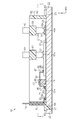
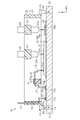
- FIG. 2 is a cross-sectional view taken along line 2-2 of FIG. 1 showing a semiconductor module.
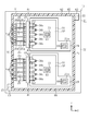
- FIG. 3 is a cross-sectional view taken along line 3-3 of FIG. 2 showing a semiconductor module.
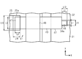
- the top view which expands and shows a conductive plate.
- FIG. 7 is a diagram showing a process of manufacturing the semiconductor module.
- the semiconductor module 10 includes a substrate 21 arranged horizontally, two bare chips (semiconductor elements) 31 mounted on the substrate 21, and a case 61 fixed to the substrate 21. ing. Moreover, the semiconductor module 10 is provided with the sealing resin which is not shown in figure.
- the horizontal plane is defined by orthogonal X and Y directions, and the vertical direction is defined by the Z direction.
- the substrate 21 has an insulating substrate 22. Through holes 23 penetrating in the vertical direction (Z direction) are provided at two places of the insulating substrate 22.
- One conductor pattern 24 and five signal patterns 25 are provided on the upper surface of the insulating substrate 22 corresponding to each of the bare chips 31. That is, a total of two conductor patterns 24 and ten signal patterns 25 are provided on the insulating substrate 22.
- Each signal pattern 25 extends in the X direction, and ten signal patterns 25 are arranged in parallel in the Y direction.
- Each conductor pattern 24 is provided with a pad 24 a. Further, pads 25a and 25b are provided at two positions of each of the signal patterns 25.
- a bare chip 31 is bonded to each conductor pattern 24.
- the bare chip 31 of the present embodiment is a vertical power MOSFET.
- each bare chip 31 has a source electrode 33 as an electrode disposed on the upper surface 32, and signal electrodes 34a, 34b, 34c, 34d, 34e.
- the signal electrodes 34a, 34b, 34c, 34d, 34e of the plurality of electrodes 33, 34a, 34b, 34c, 34d, 34e are arranged in the Y direction. That is, for each bare chip 31, a plurality of signal electrodes 34a, 34b, 34c, 34d, 34e are provided.
- the signal electrode 34a is a control signal electrode (gate electrode).
- the signal electrodes 34b and 34c are positive and negative electrodes for temperature sensing.
- the signal electrodes 34d and 34e are positive and negative electrodes for current sensing.
- the areas of the signal electrodes 34a, 34b, 34c, 34d, 34e are the same. Also, the signal electrode 34a is compared with the area of the source electrode 33 which is another electrode of the plurality of electrodes 33, 34a, 34b, 34c, 34d, 34e disposed on the upper surface 32 of the bare chip 31. The area of is small.
- the bare chip 31 has a drain electrode 36 as an electrode disposed on the lower surface 35.
- the drain electrode 36 is provided over the entire lower surface 35.
- the drain electrode 36 of each bare chip 31 is bonded to the conductor pattern 24 by a conductive bonding material (not shown) such as solder.
- two conductive plate assemblies 41 in which conductive plates (bus bars) 42 as five conductive portions are integrated by one insulating member 48 are provided on the upper surface side of the substrate 21. There is.
- the conductive plate 42 is disposed in each of the plurality of signal electrodes 34a, 34b, 34c, 34d, 34e.
- the signal electrodes 34 a, 34 b, 34 c, 34 d, 34 e of the bare chips 31 and the signal patterns 25 are connected by the conductive plate 42.
- the signal pattern 25 connected to the signal electrode 34a by the conductive plate 42 is the control signal pattern.
- the conductive plate 42 is formed by bending a metal plate, and has a rectangular connecting portion 43, a first extending portion 44, a second extending portion 45, and a first connecting portion 43. And a second joint 47.
- the connection portion 43 extends in the X direction.
- the extension portions 44 and 45 extend downward from both ends of the connection portion 43.
- the first joint portion 46 extends in the X direction from the lower end portion of the first extending portion 44.
- the second joint portion 47 extends in the X direction from the lower end portion of the second extending portion 45.
- the connection portion 43 is provided between the first joint 46 and the second joint 47.
- the connecting portion 43 electrically connects the first bonding portion 46 and the second bonding portion 47 via the first extending portion 44 and the second extending portion 45.
- the dimension of the first extending portion 44 in the vertical direction (Z direction) is shorter than the dimension of the second extending portion 45 in the vertical direction (Z direction).
- the area of the first bonding portion 46 represented by L1 ⁇ L2 is smaller than the area of the second bonding portion 47 represented by L3 ⁇ L4. Furthermore, the area of the signal electrodes 34a, 34b, 34c, 34d, 34e represented by L11 ⁇ L12 is smaller than the area of the pad 25a represented by L13 ⁇ L14.
- an insulating member 48 is provided at the connecting portion 43 of each conductive plate 42.
- One insulating member 48 is provided for the five conductive plates 42, and the connection portion 43 of each conductive plate 42 penetrates the insulating member 48.
- a portion of the insulating member 48 is provided between the first extending portion 44 and the second extending portion 45.
- the insulating member 48 is made of resin.
- the five conductive plates 42 are fixed to the insulating member 48 in a state of being kept spaced from each other in the Y direction and integrated (assembled).
- the distance between the first bonding portions 46 of the conductive plates 42 is the same as the distance between the signal electrodes 34 a, 34 b, 34 c, 34 d, 34 e of each bare chip 31, and the second bonding of the conductive plates 42 is performed.
- the spacing between the portions 47 is the same as the spacing between the pads 25 a of the signal patterns 25.
- Each conductive plate 42 is disposed such that the first bonding portion 46 faces the signal electrodes 34 a, 34 b, 34 c, 34 d, 34 e and the second bonding portion 47 faces the pads 25 a of the signal pattern 25. ing.
- the first bonding portion 46 is bonded to the signal electrodes 34 a, 34 b, 34 c, 34 d, 34 e by the solder 51, and the second bonding portion 47 is bonded to the pad 25 a of the signal pattern 25 by the solder 52.
- the solder 51 has a fillet formed between the signal electrodes 34 a, 34 b, 34 c, 34 d, 34 e and the first bonding portion 46.
- the surface facing the substrate 21 is bonded to the insulating substrate 22 by an adhesive 49.
- the case 61 is disposed on the upper surface of the substrate 21.
- the case 61 has a square frame-shaped main body 62 and protrusions 63 provided at two corners on the outer surface of the main body 62.
- a projection 64 projects downward from the projection 63.
- the distance between the two protrusions 64 is the same as the distance between the through holes 23 provided in the insulating substrate 22. Also, the size of the two protrusions 64 is such that it can be inserted into the through hole 23.
- the main body 62 has a pair of wall portions 65 and 66 extending in the X direction and a pair of wall portions 70 and 71 extending in the Y direction, and two opposing first and second wall portions 65 and 66 are provided. Support walls 67 and 68 are installed. Two leads 69 are fixed to the support walls 67 and 68, respectively, extending in the vertical direction (Z direction).
- each lead 69 is columnar and has an R shape at its lower end 69a. Specifically, each lead 69 has a quadrangular prism shape except for the lower end 69a, and the lower end 69a has an arc shape. Each lead 69 passes through each support wall 67, 68. Each lead 69 is integrally formed by the case 61.
- the third wall portion 70 is provided with a signal terminal 72.
- Five signal terminals 72 are provided corresponding to each bare chip 31, and a total of ten signal terminals 72 are provided in the Y direction.
- the signal terminal 72 is rod-shaped, and is L-shaped with its lower end bent at a right angle. The lower end of each signal terminal 72 protrudes from the third wall 70 toward the inside of the main body 62. Each signal terminal 72 is integrated with the case 61.
- the leads 69 and the signal terminals 72 extend from the substrate 21 in the vertical direction (Z direction), and do not protrude in the horizontal direction of the substrate 21 when the substrate 21 is viewed in plan.
- the two projections 64 of the case 61 are inserted into the two through holes 23 of the insulating substrate 22.
- the wall portions 65, 66, 70, 71 of the case 61 are bonded to the insulating substrate 22 by an adhesive (not shown).
- Each lead 69 integrated with the support wall 67 approaches on the source electrode 33.
- the lower end 69 a of the lead 69 is joined to the source electrode 33 by the solder 53 in a state where the lower end 69 a is not in contact with the source electrode 33. For this reason, the lower end 69a joined to the source electrode 33 is a junction.
- the solder 53 has a fillet formed thereon.
- Each lead 69 integrated with the support wall 68 approaches the pad 24 a of the conductor pattern 24.
- the leads 69 are joined by the solder 54 without contacting the pads 24a.
- the solder 54 has a fillet formed thereon.
- each signal terminal 72 integrated in the case 61 is positioned to face the pad 25 b of each signal pattern 25.
- the lower end of the signal terminal 72 is joined to the pad 25 b of each signal pattern 25 by solder 55.
- the operation of the semiconductor module 10 of the present embodiment will be described.
- the first bonding portion 46 of the conductive plate 42 is bonded to the signal electrodes 34a, 34b, 34c, 34d, 34e by solder, and the second bonding portion 47 of the conductive plate 42 is soldered It joins to the pad 25a of the pattern 25 for signals by this. The details will be described below.
- solder pastes 51a and 52a are disposed on signal electrodes 34a, 34b, 34c, 34d and 34e and pads 25a, and solder pastes 51a and 52a are formed.
- the first joint 46 and the second joint 47 of the conductive plate 42 are disposed in At this time, the insulating member 48 is bonded to the insulating substrate 22 by the adhesive 49.
- the solder pastes 53a, 54a, 55a are disposed on the source electrode 33 and the pads 24a, 25b. Then, by arranging the case 61 so that the projection 64 of the case 61 is inserted into the through hole 23 of the insulating substrate 22, the positioning between each lead 69 and each signal terminal 72 is performed. The lower end 69a of each lead 69 and the lower end of each signal terminal 72 contact the solder pastes 53a, 54a, 55a.
- solder pastes 51a, 52a, 53a, 54a, 55a are melted in a reflow furnace or the like, and then cured to form the conductive plates 42, the leads 69, and the signal terminals 72 as the solder 51, 52, 53, 54, Bonded by 55.
- Each conductive plate 42 needs to stand on the solder pastes 51 a and 52 a before being joined by the solders 51 and 52.
- the load of the insulating member 48 is applied to the conductive plate 42 by providing the connecting member 43 with the insulating member 48. For this reason, compared with the case where the insulating member 48 is not provided, the load applied from the conductive plate 42 toward the substrate 21 is large, and the center of gravity is stabilized. Therefore, the conductive plate 42 is less likely to fall. Furthermore, since the insulating member 48 is bonded to the insulating substrate 22 in the present embodiment, the overturning of the conductive plate 42 is further suppressed.
- the Manhattan phenomenon may occur due to the surface tension of the melted solder pastes 51a and 52a when the solder pastes 51a and 52a are melted, but the load of the insulating member 48 is applied to the conductive plate 42. The occurrence of the phenomenon is also suppressed.
- the connecting member 43 of the conductive plate 42 is provided with the insulating member 48. Therefore, the load of the insulating member 48 is applied to the conductive plate 42, and the conductive plate 42 is prevented from tipping before bonding by the solders 51 and 52.
- the insulating member 48 is bonded to the insulating substrate 22 by the adhesive 49. For this reason, it is further suppressed that the conductive plate 42 falls.
- the plurality of conductive plates 42 are integrated by the insulating member 48. Therefore, there is no need to position the conductive plates 42 individually when joining the conductive plates 42, and it is easy to position the plurality of conductive plates 42.
- the lower end 69 a of the lead 69 is separated from the source electrode 33. Therefore, damage to the source electrode 33 due to contact with the lead 69 is suppressed.
- the lower end 69a of the lead 69 has an R shape. Therefore, fillets are easily formed on the solder 53 for joining the lead 69 and the source electrode 33 and the solder 54 for joining the lead 69 and the pad 24a.
- the embodiment may be modified as follows.
- the insulating member 48 may not be bonded to the insulating substrate 22.
- the insulating member 48 may or may not be in surface contact with the insulating substrate 22.
- the load of the insulating member 48 is applied to the conductive plate 42, whereby the conductive plate 42 is prevented from tipping before being joined by the solders 51 and 52.
- the contact area between the insulating member 48 and the insulating substrate 22 is increased, so that the conductive plate 42 is unlikely to tip over.
- the insulating members may be individually provided on the respective conductive plates 42. That is, the plurality of conductive plates 42 may not be integrated.
- the number of conductive plates 42 may be appropriately changed in accordance with the number of signal electrodes 34a, 34b, 34c, 34d, 34e.
- the adhesive for bonding the insulating member 48 and the insulating substrate 22 may evaporate in a soldering process or the like.
- the insulating member 48 is an insulating material, it may be manufactured other than resin.
- the insulating member 48 may be bonded to the case 61.
- the lower end 69 a of the lead 69 may be in contact with the source electrode 33.
- the lead 69 and the signal terminal 72 may not be integrated with the case 61.
- the lower end 69a of the lead 69 may not have an R shape such as a flat shape.
- the bare chip 31 may be an IGBT (insulated gate bipolar transistor).
- the number of bare chips 31, the number of conductor patterns 24, the number of leads 69, and the like may be changed as appropriate.
- the insulating member is provided in the main body of the chip capacitor having the first joint, the second joint, and the main body provided between the first joint and the second joint. Good.
- the areas of the signal electrodes 34a, 34b, 34c, 34d, 34e may not be the same.
- the distance between the first bonding portions 46 of the conductive plates 42 may not be the same as the distance between the signal electrodes 34 a, 34 b, 34 c, 34 d, 34 e of the bare chips 31.
- the distance between the second bonding portions 47 of the conductive plates 42 may not be the same as the distance between the pads 25 a of the signal patterns 25.
- the area of the first bonding portion 46 may be equal to or larger than the area of the second bonding portion 47.
Landscapes
- Engineering & Computer Science (AREA)
- Microelectronics & Electronic Packaging (AREA)
- Power Engineering (AREA)
- Computer Hardware Design (AREA)
- Physics & Mathematics (AREA)
- Condensed Matter Physics & Semiconductors (AREA)
- General Physics & Mathematics (AREA)
- Geometry (AREA)
- Structures For Mounting Electric Components On Printed Circuit Boards (AREA)
Priority Applications (4)
| Application Number | Priority Date | Filing Date | Title |
|---|---|---|---|
| KR1020197002978A KR20190024993A (ko) | 2016-08-03 | 2017-05-12 | 반도체 모듈 |
| CN201780047686.1A CN109564912A (zh) | 2016-08-03 | 2017-05-12 | 半导体模块 |
| US16/322,401 US10770400B2 (en) | 2016-08-03 | 2017-05-12 | Semiconductor module |
| EP17836570.6A EP3496141A4 (en) | 2016-08-03 | 2017-05-12 | SEMICONDUCTOR MODULE |
Applications Claiming Priority (2)
| Application Number | Priority Date | Filing Date | Title |
|---|---|---|---|
| JP2016-153084 | 2016-08-03 | ||
| JP2016153084A JP6717103B2 (ja) | 2016-08-03 | 2016-08-03 | 半導体モジュール |
Publications (1)
| Publication Number | Publication Date |
|---|---|
| WO2018025463A1 true WO2018025463A1 (ja) | 2018-02-08 |
Family
ID=61074071
Family Applications (1)
| Application Number | Title | Priority Date | Filing Date |
|---|---|---|---|
| PCT/JP2017/018052 Ceased WO2018025463A1 (ja) | 2016-08-03 | 2017-05-12 | 半導体モジュール |
Country Status (6)
| Country | Link |
|---|---|
| US (1) | US10770400B2 (enExample) |
| EP (1) | EP3496141A4 (enExample) |
| JP (1) | JP6717103B2 (enExample) |
| KR (1) | KR20190024993A (enExample) |
| CN (1) | CN109564912A (enExample) |
| WO (1) | WO2018025463A1 (enExample) |
Citations (2)
| Publication number | Priority date | Publication date | Assignee | Title |
|---|---|---|---|---|
| WO2016024445A1 (ja) * | 2014-08-12 | 2016-02-18 | 富士電機株式会社 | 半導体装置 |
| WO2016059902A1 (ja) * | 2014-10-15 | 2016-04-21 | 住友電気工業株式会社 | 半導体モジュール |
Family Cites Families (11)
| Publication number | Priority date | Publication date | Assignee | Title |
|---|---|---|---|---|
| JP3614386B2 (ja) | 2001-08-23 | 2005-01-26 | 株式会社ルネサステクノロジ | パワーmosfet |
| JP3904541B2 (ja) * | 2003-09-26 | 2007-04-11 | 沖電気工業株式会社 | 半導体装置内蔵基板の製造方法 |
| JP2007288044A (ja) * | 2006-04-19 | 2007-11-01 | Sumitomo Electric Ind Ltd | 半導体装置 |
| JP5268786B2 (ja) * | 2009-06-04 | 2013-08-21 | 三菱電機株式会社 | 半導体モジュール |
| JP5659663B2 (ja) * | 2010-09-28 | 2015-01-28 | 富士電機株式会社 | 半導体装置及び半導体装置の製造方法 |
| JP2012151353A (ja) * | 2011-01-20 | 2012-08-09 | Sharp Corp | 半導体モジュール |
| CN102148215B (zh) * | 2011-01-21 | 2012-06-06 | 哈尔滨理工大学 | 提高ccga 器件软钎焊焊点可靠性的互连结构及实现方法 |
| JP2013004943A (ja) | 2011-06-22 | 2013-01-07 | Renesas Electronics Corp | 半導体装置及びその製造方法 |
| JP5708359B2 (ja) * | 2011-08-11 | 2015-04-30 | 株式会社デンソー | 半導体装置及び半導体装置の製造方法 |
| JP2015080383A (ja) | 2013-10-18 | 2015-04-23 | 日本精工株式会社 | 半導体モジュール |
| WO2015178296A1 (ja) * | 2014-05-20 | 2015-11-26 | 三菱電機株式会社 | 電力用半導体装置 |
-
2016
- 2016-08-03 JP JP2016153084A patent/JP6717103B2/ja not_active Expired - Fee Related
-
2017
- 2017-05-12 EP EP17836570.6A patent/EP3496141A4/en not_active Withdrawn
- 2017-05-12 KR KR1020197002978A patent/KR20190024993A/ko not_active Abandoned
- 2017-05-12 US US16/322,401 patent/US10770400B2/en not_active Expired - Fee Related
- 2017-05-12 CN CN201780047686.1A patent/CN109564912A/zh not_active Withdrawn
- 2017-05-12 WO PCT/JP2017/018052 patent/WO2018025463A1/ja not_active Ceased
Patent Citations (2)
| Publication number | Priority date | Publication date | Assignee | Title |
|---|---|---|---|---|
| WO2016024445A1 (ja) * | 2014-08-12 | 2016-02-18 | 富士電機株式会社 | 半導体装置 |
| WO2016059902A1 (ja) * | 2014-10-15 | 2016-04-21 | 住友電気工業株式会社 | 半導体モジュール |
Non-Patent Citations (1)
| Title |
|---|
| See also references of EP3496141A4 * |
Also Published As
| Publication number | Publication date |
|---|---|
| EP3496141A4 (en) | 2019-07-17 |
| JP6717103B2 (ja) | 2020-07-01 |
| KR20190024993A (ko) | 2019-03-08 |
| EP3496141A1 (en) | 2019-06-12 |
| US20190172788A1 (en) | 2019-06-06 |
| JP2018022777A (ja) | 2018-02-08 |
| US10770400B2 (en) | 2020-09-08 |
| CN109564912A (zh) | 2019-04-02 |
Similar Documents
| Publication | Publication Date | Title |
|---|---|---|
| CN103650082B (zh) | 电子部件 | |
| JP6850938B1 (ja) | 半導体装置、及びリードフレーム材 | |
| US9000571B2 (en) | Surface-mounting light emitting diode device and method for manufacturing the same | |
| JP6226068B2 (ja) | 半導体装置 | |
| JP2016213308A (ja) | プリント回路板及びプリント配線板 | |
| JP2018006697A (ja) | 半導体モジュール | |
| WO2014190645A1 (zh) | 堆叠式封装结构 | |
| JP2012212712A (ja) | 半導体装置の実装構造及び半導体装置の実装方法 | |
| KR20170081242A (ko) | 전자 제어 장치 | |
| KR20040073942A (ko) | 반도체장치 | |
| JP6717103B2 (ja) | 半導体モジュール | |
| WO2019012849A1 (ja) | 電子回路基板 | |
| JP5962364B2 (ja) | パワー半導体モジュール | |
| JP6311568B2 (ja) | 電子装置 | |
| WO2020090411A1 (ja) | 半導体装置 | |
| JP2013175556A (ja) | 圧電トランス及び圧電トランスの実装方法 | |
| JP2006060106A (ja) | リード部材及び表面実装型半導体装置 | |
| KR20150139190A (ko) | 소자 및 소자 패키지 | |
| CN111343783A (zh) | 印刷基板 | |
| KR20130074490A (ko) | 인쇄회로기판 사이의 연결 구조 | |
| JP7085974B2 (ja) | 半導体装置 | |
| JP6907893B2 (ja) | 半導体装置 | |
| TW202535110A (zh) | 電子模組 | |
| TW202534905A (zh) | 電子模組 | |
| JPH0247109B2 (enExample) |
Legal Events
| Date | Code | Title | Description |
|---|---|---|---|
| 121 | Ep: the epo has been informed by wipo that ep was designated in this application |
Ref document number: 17836570 Country of ref document: EP Kind code of ref document: A1 |
|
| ENP | Entry into the national phase |
Ref document number: 20197002978 Country of ref document: KR Kind code of ref document: A |
|
| NENP | Non-entry into the national phase |
Ref country code: DE |
|
| ENP | Entry into the national phase |
Ref document number: 2017836570 Country of ref document: EP Effective date: 20190304 |