WO2018003565A1 - Support de fabrication de boîtiers de semi-conducteurs, son utilisation et procédé de fabrication de boîtiers de semi-conducteurs - Google Patents
Support de fabrication de boîtiers de semi-conducteurs, son utilisation et procédé de fabrication de boîtiers de semi-conducteurs Download PDFInfo
- Publication number
- WO2018003565A1 WO2018003565A1 PCT/JP2017/022504 JP2017022504W WO2018003565A1 WO 2018003565 A1 WO2018003565 A1 WO 2018003565A1 JP 2017022504 W JP2017022504 W JP 2017022504W WO 2018003565 A1 WO2018003565 A1 WO 2018003565A1
- Authority
- WO
- WIPO (PCT)
- Prior art keywords
- support
- manufacturing
- semiconductor package
- treatment
- semiconductor
- Prior art date
Links
- 239000004065 semiconductor Substances 0.000 title claims abstract description 169
- 238000004519 manufacturing process Methods 0.000 title claims abstract description 106
- 238000000034 method Methods 0.000 title claims abstract description 80
- 239000010410 layer Substances 0.000 claims abstract description 103
- 229920005989 resin Polymers 0.000 claims abstract description 102
- 239000011347 resin Substances 0.000 claims abstract description 102
- 125000002723 alicyclic group Chemical group 0.000 claims abstract description 56
- 239000012790 adhesive layer Substances 0.000 claims abstract description 25
- 238000012545 processing Methods 0.000 claims abstract description 24
- 238000010438 heat treatment Methods 0.000 claims abstract description 22
- 238000007747 plating Methods 0.000 claims abstract description 21
- 238000011161 development Methods 0.000 claims abstract description 16
- 238000005498 polishing Methods 0.000 claims abstract description 16
- 238000011282 treatment Methods 0.000 claims description 55
- 239000000463 material Substances 0.000 claims description 23
- 238000009489 vacuum treatment Methods 0.000 claims description 9
- 238000000465 moulding Methods 0.000 claims description 7
- 229920000642 polymer Polymers 0.000 description 86
- 239000010408 film Substances 0.000 description 48
- 239000000178 monomer Substances 0.000 description 44
- JFNLZVQOOSMTJK-KNVOCYPGSA-N norbornene Chemical compound C1[C@@H]2CC[C@H]1C=C2 JFNLZVQOOSMTJK-KNVOCYPGSA-N 0.000 description 28
- 239000004820 Pressure-sensitive adhesive Substances 0.000 description 24
- HECLRDQVFMWTQS-RGOKHQFPSA-N 1755-01-7 Chemical compound C1[C@H]2[C@@H]3CC=C[C@@H]3[C@@H]1C=C2 HECLRDQVFMWTQS-RGOKHQFPSA-N 0.000 description 20
- -1 monocyclic olefin Chemical class 0.000 description 19
- 229920001971 elastomer Polymers 0.000 description 18
- 239000000047 product Substances 0.000 description 18
- 239000005060 rubber Substances 0.000 description 18
- 239000000243 solution Substances 0.000 description 18
- 239000000126 substance Substances 0.000 description 17
- XLYOFNOQVPJJNP-UHFFFAOYSA-N water Substances O XLYOFNOQVPJJNP-UHFFFAOYSA-N 0.000 description 16
- 238000007142 ring opening reaction Methods 0.000 description 14
- 238000010521 absorption reaction Methods 0.000 description 13
- PPBRXRYQALVLMV-UHFFFAOYSA-N Styrene Chemical compound C=CC1=CC=CC=C1 PPBRXRYQALVLMV-UHFFFAOYSA-N 0.000 description 12
- 239000010949 copper Substances 0.000 description 12
- WGTYBPLFGIVFAS-UHFFFAOYSA-M tetramethylammonium hydroxide Chemical compound [OH-].C[N+](C)(C)C WGTYBPLFGIVFAS-UHFFFAOYSA-M 0.000 description 10
- 239000000654 additive Substances 0.000 description 9
- 239000000853 adhesive Substances 0.000 description 9
- 230000001070 adhesive effect Effects 0.000 description 9
- 238000007789 sealing Methods 0.000 description 9
- 238000001035 drying Methods 0.000 description 8
- 150000004678 hydrides Chemical class 0.000 description 8
- 238000005984 hydrogenation reaction Methods 0.000 description 8
- 238000007151 ring opening polymerisation reaction Methods 0.000 description 8
- 239000004642 Polyimide Substances 0.000 description 7
- 239000003054 catalyst Substances 0.000 description 7
- 239000011248 coating agent Substances 0.000 description 7
- 238000000576 coating method Methods 0.000 description 7
- 230000009477 glass transition Effects 0.000 description 7
- 238000002844 melting Methods 0.000 description 7
- 230000008018 melting Effects 0.000 description 7
- 239000004014 plasticizer Substances 0.000 description 7
- 229920001721 polyimide Polymers 0.000 description 7
- 125000001424 substituent group Chemical group 0.000 description 7
- 229920002554 vinyl polymer Polymers 0.000 description 7
- 238000006243 chemical reaction Methods 0.000 description 6
- 239000003795 chemical substances by application Substances 0.000 description 6
- 150000001875 compounds Chemical class 0.000 description 6
- HGCIXCUEYOPUTN-UHFFFAOYSA-N cyclohexene Chemical compound C1CCC=CC1 HGCIXCUEYOPUTN-UHFFFAOYSA-N 0.000 description 6
- 150000001993 dienes Chemical class 0.000 description 6
- 239000010936 titanium Substances 0.000 description 6
- 239000006096 absorbing agent Substances 0.000 description 5
- 239000003963 antioxidant agent Substances 0.000 description 5
- 239000004020 conductor Substances 0.000 description 5
- 239000003063 flame retardant Substances 0.000 description 5
- 239000007788 liquid Substances 0.000 description 5
- 229910052751 metal Inorganic materials 0.000 description 5
- 239000002184 metal Substances 0.000 description 5
- 239000000203 mixture Substances 0.000 description 5
- 238000004544 sputter deposition Methods 0.000 description 5
- 229920006132 styrene block copolymer Polymers 0.000 description 5
- 230000002194 synthesizing effect Effects 0.000 description 5
- 238000005406 washing Methods 0.000 description 5
- WLTSXAIICPDFKI-FNORWQNLSA-N (E)-3-dodecene Chemical compound CCCCCCCC\C=C\CC WLTSXAIICPDFKI-FNORWQNLSA-N 0.000 description 4
- LIKMAJRDDDTEIG-UHFFFAOYSA-N 1-hexene Chemical compound CCCCC=C LIKMAJRDDDTEIG-UHFFFAOYSA-N 0.000 description 4
- 239000004215 Carbon black (E152) Substances 0.000 description 4
- RYGMFSIKBFXOCR-UHFFFAOYSA-N Copper Chemical compound [Cu] RYGMFSIKBFXOCR-UHFFFAOYSA-N 0.000 description 4
- XEEYBQQBJWHFJM-UHFFFAOYSA-N Iron Chemical compound [Fe] XEEYBQQBJWHFJM-UHFFFAOYSA-N 0.000 description 4
- PXHVJJICTQNCMI-UHFFFAOYSA-N Nickel Chemical compound [Ni] PXHVJJICTQNCMI-UHFFFAOYSA-N 0.000 description 4
- XUIMIQQOPSSXEZ-UHFFFAOYSA-N Silicon Chemical compound [Si] XUIMIQQOPSSXEZ-UHFFFAOYSA-N 0.000 description 4
- WYURNTSHIVDZCO-UHFFFAOYSA-N Tetrahydrofuran Chemical compound C1CCOC1 WYURNTSHIVDZCO-UHFFFAOYSA-N 0.000 description 4
- NIXOWILDQLNWCW-UHFFFAOYSA-N acrylic acid group Chemical group C(C=C)(=O)O NIXOWILDQLNWCW-UHFFFAOYSA-N 0.000 description 4
- 230000000996 additive effect Effects 0.000 description 4
- 239000002216 antistatic agent Substances 0.000 description 4
- 239000007864 aqueous solution Substances 0.000 description 4
- 229910052802 copper Inorganic materials 0.000 description 4
- 239000003431 cross linking reagent Substances 0.000 description 4
- 125000004122 cyclic group Chemical group 0.000 description 4
- 238000009826 distribution Methods 0.000 description 4
- 239000003822 epoxy resin Substances 0.000 description 4
- 239000000945 filler Substances 0.000 description 4
- 238000005227 gel permeation chromatography Methods 0.000 description 4
- 229930195733 hydrocarbon Natural products 0.000 description 4
- 239000004611 light stabiliser Substances 0.000 description 4
- 238000005259 measurement Methods 0.000 description 4
- 238000007517 polishing process Methods 0.000 description 4
- 229920000647 polyepoxide Polymers 0.000 description 4
- 238000006116 polymerization reaction Methods 0.000 description 4
- 229920001296 polysiloxane Polymers 0.000 description 4
- 229910052710 silicon Inorganic materials 0.000 description 4
- 239000010703 silicon Substances 0.000 description 4
- 239000000758 substrate Substances 0.000 description 4
- 229920002799 BoPET Polymers 0.000 description 3
- XDTMQSROBMDMFD-UHFFFAOYSA-N Cyclohexane Chemical compound C1CCCCC1 XDTMQSROBMDMFD-UHFFFAOYSA-N 0.000 description 3
- 229920002367 Polyisobutene Polymers 0.000 description 3
- YXFVVABEGXRONW-UHFFFAOYSA-N Toluene Chemical compound CC1=CC=CC=C1 YXFVVABEGXRONW-UHFFFAOYSA-N 0.000 description 3
- YRKCREAYFQTBPV-UHFFFAOYSA-N acetylacetone Natural products CC(=O)CC(C)=O YRKCREAYFQTBPV-UHFFFAOYSA-N 0.000 description 3
- 238000012644 addition polymerization Methods 0.000 description 3
- 230000003712 anti-aging effect Effects 0.000 description 3
- 229920005601 base polymer Polymers 0.000 description 3
- 230000015572 biosynthetic process Effects 0.000 description 3
- 239000005388 borosilicate glass Substances 0.000 description 3
- MTAZNLWOLGHBHU-UHFFFAOYSA-N butadiene-styrene rubber Chemical compound C=CC=C.C=CC1=CC=CC=C1 MTAZNLWOLGHBHU-UHFFFAOYSA-N 0.000 description 3
- 125000004432 carbon atom Chemical group C* 0.000 description 3
- 230000000052 comparative effect Effects 0.000 description 3
- 238000005520 cutting process Methods 0.000 description 3
- URYYVOIYTNXXBN-UPHRSURJSA-N cyclooctene Chemical compound C1CCC\C=C/CC1 URYYVOIYTNXXBN-UPHRSURJSA-N 0.000 description 3
- 239000004913 cyclooctene Substances 0.000 description 3
- 239000000975 dye Substances 0.000 description 3
- 239000011521 glass Substances 0.000 description 3
- 239000003607 modifier Substances 0.000 description 3
- 125000002950 monocyclic group Chemical group 0.000 description 3
- 239000008188 pellet Substances 0.000 description 3
- 239000000049 pigment Substances 0.000 description 3
- 239000002685 polymerization catalyst Substances 0.000 description 3
- 239000002002 slurry Substances 0.000 description 3
- 239000007787 solid Substances 0.000 description 3
- 238000004528 spin coating Methods 0.000 description 3
- 239000004094 surface-active agent Substances 0.000 description 3
- 238000012546 transfer Methods 0.000 description 3
- XWJBRBSPAODJER-UHFFFAOYSA-N 1,7-octadiene Chemical compound C=CCCCCC=C XWJBRBSPAODJER-UHFFFAOYSA-N 0.000 description 2
- 238000001644 13C nuclear magnetic resonance spectroscopy Methods 0.000 description 2
- VSKJLJHPAFKHBX-UHFFFAOYSA-N 2-methylbuta-1,3-diene;styrene Chemical compound CC(=C)C=C.C=CC1=CC=CC=C1.C=CC1=CC=CC=C1 VSKJLJHPAFKHBX-UHFFFAOYSA-N 0.000 description 2
- IJGRMHOSHXDMSA-UHFFFAOYSA-N Atomic nitrogen Chemical compound N#N IJGRMHOSHXDMSA-UHFFFAOYSA-N 0.000 description 2
- KAKZBPTYRLMSJV-UHFFFAOYSA-N Butadiene Chemical compound C=CC=C KAKZBPTYRLMSJV-UHFFFAOYSA-N 0.000 description 2
- 229920000089 Cyclic olefin copolymer Polymers 0.000 description 2
- VGGSQFUCUMXWEO-UHFFFAOYSA-N Ethene Chemical compound C=C VGGSQFUCUMXWEO-UHFFFAOYSA-N 0.000 description 2
- 239000005977 Ethylene Substances 0.000 description 2
- 244000043261 Hevea brasiliensis Species 0.000 description 2
- UFHFLCQGNIYNRP-UHFFFAOYSA-N Hydrogen Chemical compound [H][H] UFHFLCQGNIYNRP-UHFFFAOYSA-N 0.000 description 2
- RRHGJUQNOFWUDK-UHFFFAOYSA-N Isoprene Chemical compound CC(=C)C=C RRHGJUQNOFWUDK-UHFFFAOYSA-N 0.000 description 2
- 229920000459 Nitrile rubber Polymers 0.000 description 2
- KDLHZDBZIXYQEI-UHFFFAOYSA-N Palladium Chemical compound [Pd] KDLHZDBZIXYQEI-UHFFFAOYSA-N 0.000 description 2
- 239000005062 Polybutadiene Substances 0.000 description 2
- RTAQQCXQSZGOHL-UHFFFAOYSA-N Titanium Chemical compound [Ti] RTAQQCXQSZGOHL-UHFFFAOYSA-N 0.000 description 2
- QCWXUUIWCKQGHC-UHFFFAOYSA-N Zirconium Chemical compound [Zr] QCWXUUIWCKQGHC-UHFFFAOYSA-N 0.000 description 2
- 229920001400 block copolymer Polymers 0.000 description 2
- 229920005549 butyl rubber Polymers 0.000 description 2
- CREMABGTGYGIQB-UHFFFAOYSA-N carbon carbon Chemical compound C.C CREMABGTGYGIQB-UHFFFAOYSA-N 0.000 description 2
- 239000011203 carbon fibre reinforced carbon Substances 0.000 description 2
- 238000007906 compression Methods 0.000 description 2
- 230000006835 compression Effects 0.000 description 2
- 229920001577 copolymer Polymers 0.000 description 2
- 150000001924 cycloalkanes Chemical group 0.000 description 2
- 150000001925 cycloalkenes Chemical group 0.000 description 2
- 125000000753 cycloalkyl group Chemical group 0.000 description 2
- ZXIJMRYMVAMXQP-UHFFFAOYSA-N cycloheptene Chemical compound C1CCC=CCC1 ZXIJMRYMVAMXQP-UHFFFAOYSA-N 0.000 description 2
- MGNZXYYWBUKAII-UHFFFAOYSA-N cyclohexa-1,3-diene Chemical compound C1CC=CC=C1 MGNZXYYWBUKAII-UHFFFAOYSA-N 0.000 description 2
- ZSWFCLXCOIISFI-UHFFFAOYSA-N cyclopentadiene Chemical compound C1C=CC=C1 ZSWFCLXCOIISFI-UHFFFAOYSA-N 0.000 description 2
- LPIQUOYDBNQMRZ-UHFFFAOYSA-N cyclopentene Chemical compound C1CC=CC1 LPIQUOYDBNQMRZ-UHFFFAOYSA-N 0.000 description 2
- 238000007772 electroless plating Methods 0.000 description 2
- 238000005530 etching Methods 0.000 description 2
- HQQADJVZYDDRJT-UHFFFAOYSA-N ethene;prop-1-ene Chemical group C=C.CC=C HQQADJVZYDDRJT-UHFFFAOYSA-N 0.000 description 2
- 238000009474 hot melt extrusion Methods 0.000 description 2
- 229910052739 hydrogen Inorganic materials 0.000 description 2
- 239000001257 hydrogen Substances 0.000 description 2
- 229910052742 iron Inorganic materials 0.000 description 2
- 229910001507 metal halide Inorganic materials 0.000 description 2
- 150000005309 metal halides Chemical class 0.000 description 2
- VNWKTOKETHGBQD-UHFFFAOYSA-N methane Chemical compound C VNWKTOKETHGBQD-UHFFFAOYSA-N 0.000 description 2
- VLKZOEOYAKHREP-UHFFFAOYSA-N n-Hexane Chemical compound CCCCCC VLKZOEOYAKHREP-UHFFFAOYSA-N 0.000 description 2
- 229920003052 natural elastomer Polymers 0.000 description 2
- 229920001194 natural rubber Polymers 0.000 description 2
- YWAKXRMUMFPDSH-UHFFFAOYSA-N pentene Chemical compound CCCC=C YWAKXRMUMFPDSH-UHFFFAOYSA-N 0.000 description 2
- 229920000058 polyacrylate Polymers 0.000 description 2
- 229920002857 polybutadiene Polymers 0.000 description 2
- 229920000139 polyethylene terephthalate Polymers 0.000 description 2
- 239000005020 polyethylene terephthalate Substances 0.000 description 2
- 230000000379 polymerizing effect Effects 0.000 description 2
- 230000003014 reinforcing effect Effects 0.000 description 2
- 150000003839 salts Chemical class 0.000 description 2
- 229910000679 solder Inorganic materials 0.000 description 2
- 239000002904 solvent Substances 0.000 description 2
- 238000004381 surface treatment Methods 0.000 description 2
- 238000003786 synthesis reaction Methods 0.000 description 2
- YLQBMQCUIZJEEH-UHFFFAOYSA-N tetrahydrofuran Natural products C=1C=COC=1 YLQBMQCUIZJEEH-UHFFFAOYSA-N 0.000 description 2
- 229920001187 thermosetting polymer Polymers 0.000 description 2
- 239000010409 thin film Substances 0.000 description 2
- 229910052719 titanium Inorganic materials 0.000 description 2
- 125000000391 vinyl group Chemical group [H]C([*])=C([H])[H] 0.000 description 2
- 229910052726 zirconium Inorganic materials 0.000 description 2
- 239000004711 α-olefin Substances 0.000 description 2
- LCSLWNXVIDKVGD-KQQUZDAGSA-N (3e,7e)-deca-3,7-diene Chemical compound CC\C=C\CC\C=C\CC LCSLWNXVIDKVGD-KQQUZDAGSA-N 0.000 description 1
- JBVMSEMQJGGOFR-FNORWQNLSA-N (4e)-4-methylhexa-1,4-diene Chemical compound C\C=C(/C)CC=C JBVMSEMQJGGOFR-FNORWQNLSA-N 0.000 description 1
- PRBHEGAFLDMLAL-GQCTYLIASA-N (4e)-hexa-1,4-diene Chemical compound C\C=C\CC=C PRBHEGAFLDMLAL-GQCTYLIASA-N 0.000 description 1
- SDRZFSPCVYEJTP-UHFFFAOYSA-N 1-ethenylcyclohexene Chemical compound C=CC1=CCCCC1 SDRZFSPCVYEJTP-UHFFFAOYSA-N 0.000 description 1
- 238000005160 1H NMR spectroscopy Methods 0.000 description 1
- RNFJDJUURJAICM-UHFFFAOYSA-N 2,2,4,4,6,6-hexaphenoxy-1,3,5-triaza-2$l^{5},4$l^{5},6$l^{5}-triphosphacyclohexa-1,3,5-triene Chemical compound N=1P(OC=2C=CC=CC=2)(OC=2C=CC=CC=2)=NP(OC=2C=CC=CC=2)(OC=2C=CC=CC=2)=NP=1(OC=1C=CC=CC=1)OC1=CC=CC=C1 RNFJDJUURJAICM-UHFFFAOYSA-N 0.000 description 1
- 125000003903 2-propenyl group Chemical group [H]C([*])([H])C([H])=C([H])[H] 0.000 description 1
- XUFPYLQWLKKGDQ-UHFFFAOYSA-N 4,4a,9,9a-tetrahydro-1,4-methano-1h-fluorene Chemical compound C12CC3=CC=CC=C3C1C1C=CC2C1 XUFPYLQWLKKGDQ-UHFFFAOYSA-N 0.000 description 1
- VSQLAQKFRFTMNS-UHFFFAOYSA-N 5-methylhexa-1,4-diene Chemical compound CC(C)=CCC=C VSQLAQKFRFTMNS-UHFFFAOYSA-N 0.000 description 1
- LYCAIKOWRPUZTN-UHFFFAOYSA-N Ethylene glycol Chemical compound OCCO LYCAIKOWRPUZTN-UHFFFAOYSA-N 0.000 description 1
- ZOKXTWBITQBERF-UHFFFAOYSA-N Molybdenum Chemical compound [Mo] ZOKXTWBITQBERF-UHFFFAOYSA-N 0.000 description 1
- 229910002651 NO3 Inorganic materials 0.000 description 1
- NHNBFGGVMKEFGY-UHFFFAOYSA-N Nitrate Chemical compound [O-][N+]([O-])=O NHNBFGGVMKEFGY-UHFFFAOYSA-N 0.000 description 1
- 239000004793 Polystyrene Substances 0.000 description 1
- XBDQKXXYIPTUBI-UHFFFAOYSA-M Propionate Chemical compound CCC([O-])=O XBDQKXXYIPTUBI-UHFFFAOYSA-M 0.000 description 1
- 102000001708 Protein Isoforms Human genes 0.000 description 1
- 108010029485 Protein Isoforms Proteins 0.000 description 1
- KJTLSVCANCCWHF-UHFFFAOYSA-N Ruthenium Chemical compound [Ru] KJTLSVCANCCWHF-UHFFFAOYSA-N 0.000 description 1
- 125000003647 acryloyl group Chemical group O=C([*])C([H])=C([H])[H] 0.000 description 1
- 239000003463 adsorbent Substances 0.000 description 1
- 239000012670 alkaline solution Substances 0.000 description 1
- 125000004453 alkoxycarbonyl group Chemical group 0.000 description 1
- 125000000217 alkyl group Chemical group 0.000 description 1
- 125000002947 alkylene group Chemical group 0.000 description 1
- 125000001118 alkylidene group Chemical group 0.000 description 1
- XYLMUPLGERFSHI-UHFFFAOYSA-N alpha-Methylstyrene Chemical compound CC(=C)C1=CC=CC=C1 XYLMUPLGERFSHI-UHFFFAOYSA-N 0.000 description 1
- ARCGXLSVLAOJQL-UHFFFAOYSA-N anhydrous trimellitic acid Natural products OC(=O)C1=CC=C(C(O)=O)C(C(O)=O)=C1 ARCGXLSVLAOJQL-UHFFFAOYSA-N 0.000 description 1
- 230000003078 antioxidant effect Effects 0.000 description 1
- 125000003118 aryl group Chemical group 0.000 description 1
- 238000003763 carbonization Methods 0.000 description 1
- 239000012295 chemical reaction liquid Substances 0.000 description 1
- 239000003638 chemical reducing agent Substances 0.000 description 1
- 239000003086 colorant Substances 0.000 description 1
- 238000007796 conventional method Methods 0.000 description 1
- 238000007334 copolymerization reaction Methods 0.000 description 1
- 239000003484 crystal nucleating agent Substances 0.000 description 1
- CFBGXYDUODCMNS-UHFFFAOYSA-N cyclobutene Chemical compound C1CC=C1 CFBGXYDUODCMNS-UHFFFAOYSA-N 0.000 description 1
- GVRWIAHBVAYKIZ-UHFFFAOYSA-N dec-3-ene Chemical compound CCCCCCC=CCC GVRWIAHBVAYKIZ-UHFFFAOYSA-N 0.000 description 1
- 238000000113 differential scanning calorimetry Methods 0.000 description 1
- 238000007865 diluting Methods 0.000 description 1
- HNPSIPDUKPIQMN-UHFFFAOYSA-N dioxosilane;oxo(oxoalumanyloxy)alumane Chemical compound O=[Si]=O.O=[Al]O[Al]=O HNPSIPDUKPIQMN-UHFFFAOYSA-N 0.000 description 1
- 238000010894 electron beam technology Methods 0.000 description 1
- LDLDYFCCDKENPD-UHFFFAOYSA-N ethenylcyclohexane Chemical compound C=CC1CCCCC1 LDLDYFCCDKENPD-UHFFFAOYSA-N 0.000 description 1
- 125000005677 ethinylene group Chemical group [*:2]C#C[*:1] 0.000 description 1
- GCPCLEKQVMKXJM-UHFFFAOYSA-N ethoxy(diethyl)alumane Chemical compound CCO[Al](CC)CC GCPCLEKQVMKXJM-UHFFFAOYSA-N 0.000 description 1
- 125000000524 functional group Chemical group 0.000 description 1
- 238000011899 heat drying method Methods 0.000 description 1
- 125000000623 heterocyclic group Chemical group 0.000 description 1
- 239000000314 lubricant Substances 0.000 description 1
- 229910052750 molybdenum Inorganic materials 0.000 description 1
- 239000011733 molybdenum Substances 0.000 description 1
- 229910052759 nickel Inorganic materials 0.000 description 1
- 229910052757 nitrogen Inorganic materials 0.000 description 1
- 150000002848 norbornenes Chemical class 0.000 description 1
- 125000003518 norbornenyl group Chemical group C12(C=CC(CC1)C2)* 0.000 description 1
- JRZJOMJEPLMPRA-UHFFFAOYSA-N olefin Natural products CCCCCCCC=C JRZJOMJEPLMPRA-UHFFFAOYSA-N 0.000 description 1
- 230000003287 optical effect Effects 0.000 description 1
- 239000003960 organic solvent Substances 0.000 description 1
- 229910052762 osmium Inorganic materials 0.000 description 1
- SYQBFIAQOQZEGI-UHFFFAOYSA-N osmium atom Chemical compound [Os] SYQBFIAQOQZEGI-UHFFFAOYSA-N 0.000 description 1
- 229910052763 palladium Inorganic materials 0.000 description 1
- NFHFRUOZVGFOOS-UHFFFAOYSA-N palladium;triphenylphosphane Chemical compound [Pd].C1=CC=CC=C1P(C=1C=CC=CC=1)C1=CC=CC=C1.C1=CC=CC=C1P(C=1C=CC=CC=1)C1=CC=CC=C1.C1=CC=CC=C1P(C=1C=CC=CC=1)C1=CC=CC=C1.C1=CC=CC=C1P(C=1C=CC=CC=1)C1=CC=CC=C1 NFHFRUOZVGFOOS-UHFFFAOYSA-N 0.000 description 1
- 239000002245 particle Substances 0.000 description 1
- RGSFGYAAUTVSQA-UHFFFAOYSA-N pentamethylene Natural products C1CCCC1 RGSFGYAAUTVSQA-UHFFFAOYSA-N 0.000 description 1
- 229920002587 poly(1,3-butadiene) polymer Polymers 0.000 description 1
- 229920001195 polyisoprene Polymers 0.000 description 1
- 239000003505 polymerization initiator Substances 0.000 description 1
- 239000002954 polymerization reaction product Substances 0.000 description 1
- 229920000098 polyolefin Polymers 0.000 description 1
- 229920002223 polystyrene Polymers 0.000 description 1
- 229920002742 polystyrene-block-poly(ethylene/propylene) -block-polystyrene Polymers 0.000 description 1
- 238000000746 purification Methods 0.000 description 1
- CYIDZMCFTVVTJO-UHFFFAOYSA-N pyromellityc acid Natural products OC(=O)C1=CC(C(O)=O)=C(C(O)=O)C=C1C(O)=O CYIDZMCFTVVTJO-UHFFFAOYSA-N 0.000 description 1
- 229920005604 random copolymer Polymers 0.000 description 1
- 238000011160 research Methods 0.000 description 1
- 229910052707 ruthenium Inorganic materials 0.000 description 1
- VIHDTGHDWPVSMM-UHFFFAOYSA-N ruthenium;triphenylphosphane Chemical compound [Ru].C1=CC=CC=C1P(C=1C=CC=CC=1)C1=CC=CC=C1 VIHDTGHDWPVSMM-UHFFFAOYSA-N 0.000 description 1
- 229920005573 silicon-containing polymer Polymers 0.000 description 1
- 238000010183 spectrum analysis Methods 0.000 description 1
- 229910001220 stainless steel Inorganic materials 0.000 description 1
- 239000010935 stainless steel Substances 0.000 description 1
- 229920001935 styrene-ethylene-butadiene-styrene Polymers 0.000 description 1
- 229920003051 synthetic elastomer Polymers 0.000 description 1
- 239000005061 synthetic rubber Substances 0.000 description 1
- XBFJAVXCNXDMBH-UHFFFAOYSA-N tetracyclo[6.2.1.1(3,6).0(2,7)]dodec-4-ene Chemical compound C1C(C23)C=CC1C3C1CC2CC1 XBFJAVXCNXDMBH-UHFFFAOYSA-N 0.000 description 1
- PVJHFVMRMWVWAX-UHFFFAOYSA-N tetradeca-2,7,9,11-tetraene Chemical compound CCC=CC=CC=CCCCC=CC PVJHFVMRMWVWAX-UHFFFAOYSA-N 0.000 description 1
- 125000000383 tetramethylene group Chemical group [H]C([H])([*:1])C([H])([H])C([H])([H])C([H])([H])[*:2] 0.000 description 1
- 229910052723 transition metal Inorganic materials 0.000 description 1
- 150000003624 transition metals Chemical class 0.000 description 1
- WFKWXMTUELFFGS-UHFFFAOYSA-N tungsten Chemical compound [W] WFKWXMTUELFFGS-UHFFFAOYSA-N 0.000 description 1
- 229910052721 tungsten Inorganic materials 0.000 description 1
- 239000010937 tungsten Substances 0.000 description 1
- 150000003682 vanadium compounds Chemical class 0.000 description 1
- 238000004804 winding Methods 0.000 description 1
Images


Classifications
-
- H—ELECTRICITY
- H01—ELECTRIC ELEMENTS
- H01L—SEMICONDUCTOR DEVICES NOT COVERED BY CLASS H10
- H01L21/00—Processes or apparatus adapted for the manufacture or treatment of semiconductor or solid state devices or of parts thereof
- H01L21/02—Manufacture or treatment of semiconductor devices or of parts thereof
- H01L21/04—Manufacture or treatment of semiconductor devices or of parts thereof the devices having potential barriers, e.g. a PN junction, depletion layer or carrier concentration layer
- H01L21/50—Assembly of semiconductor devices using processes or apparatus not provided for in a single one of the subgroups H01L21/06 - H01L21/326, e.g. sealing of a cap to a base of a container
- H01L21/56—Encapsulations, e.g. encapsulation layers, coatings
- H01L21/568—Temporary substrate used as encapsulation process aid
-
- C—CHEMISTRY; METALLURGY
- C09—DYES; PAINTS; POLISHES; NATURAL RESINS; ADHESIVES; COMPOSITIONS NOT OTHERWISE PROVIDED FOR; APPLICATIONS OF MATERIALS NOT OTHERWISE PROVIDED FOR
- C09J—ADHESIVES; NON-MECHANICAL ASPECTS OF ADHESIVE PROCESSES IN GENERAL; ADHESIVE PROCESSES NOT PROVIDED FOR ELSEWHERE; USE OF MATERIALS AS ADHESIVES
- C09J201/00—Adhesives based on unspecified macromolecular compounds
-
- C—CHEMISTRY; METALLURGY
- C09—DYES; PAINTS; POLISHES; NATURAL RESINS; ADHESIVES; COMPOSITIONS NOT OTHERWISE PROVIDED FOR; APPLICATIONS OF MATERIALS NOT OTHERWISE PROVIDED FOR
- C09J—ADHESIVES; NON-MECHANICAL ASPECTS OF ADHESIVE PROCESSES IN GENERAL; ADHESIVE PROCESSES NOT PROVIDED FOR ELSEWHERE; USE OF MATERIALS AS ADHESIVES
- C09J7/00—Adhesives in the form of films or foils
- C09J7/20—Adhesives in the form of films or foils characterised by their carriers
- C09J7/22—Plastics; Metallised plastics
- C09J7/24—Plastics; Metallised plastics based on macromolecular compounds obtained by reactions involving only carbon-to-carbon unsaturated bonds
- C09J7/241—Polyolefin, e.g.rubber
-
- C—CHEMISTRY; METALLURGY
- C09—DYES; PAINTS; POLISHES; NATURAL RESINS; ADHESIVES; COMPOSITIONS NOT OTHERWISE PROVIDED FOR; APPLICATIONS OF MATERIALS NOT OTHERWISE PROVIDED FOR
- C09J—ADHESIVES; NON-MECHANICAL ASPECTS OF ADHESIVE PROCESSES IN GENERAL; ADHESIVE PROCESSES NOT PROVIDED FOR ELSEWHERE; USE OF MATERIALS AS ADHESIVES
- C09J7/00—Adhesives in the form of films or foils
- C09J7/20—Adhesives in the form of films or foils characterised by their carriers
- C09J7/22—Plastics; Metallised plastics
- C09J7/25—Plastics; Metallised plastics based on macromolecular compounds obtained otherwise than by reactions involving only carbon-to-carbon unsaturated bonds
-
- H—ELECTRICITY
- H01—ELECTRIC ELEMENTS
- H01L—SEMICONDUCTOR DEVICES NOT COVERED BY CLASS H10
- H01L21/00—Processes or apparatus adapted for the manufacture or treatment of semiconductor or solid state devices or of parts thereof
- H01L21/02—Manufacture or treatment of semiconductor devices or of parts thereof
- H01L21/04—Manufacture or treatment of semiconductor devices or of parts thereof the devices having potential barriers, e.g. a PN junction, depletion layer or carrier concentration layer
- H01L21/50—Assembly of semiconductor devices using processes or apparatus not provided for in a single one of the subgroups H01L21/06 - H01L21/326, e.g. sealing of a cap to a base of a container
- H01L21/52—Mounting semiconductor bodies in containers
-
- H—ELECTRICITY
- H01—ELECTRIC ELEMENTS
- H01L—SEMICONDUCTOR DEVICES NOT COVERED BY CLASS H10
- H01L21/00—Processes or apparatus adapted for the manufacture or treatment of semiconductor or solid state devices or of parts thereof
- H01L21/02—Manufacture or treatment of semiconductor devices or of parts thereof
- H01L21/04—Manufacture or treatment of semiconductor devices or of parts thereof the devices having potential barriers, e.g. a PN junction, depletion layer or carrier concentration layer
- H01L21/50—Assembly of semiconductor devices using processes or apparatus not provided for in a single one of the subgroups H01L21/06 - H01L21/326, e.g. sealing of a cap to a base of a container
- H01L21/56—Encapsulations, e.g. encapsulation layers, coatings
-
- H—ELECTRICITY
- H01—ELECTRIC ELEMENTS
- H01L—SEMICONDUCTOR DEVICES NOT COVERED BY CLASS H10
- H01L21/00—Processes or apparatus adapted for the manufacture or treatment of semiconductor or solid state devices or of parts thereof
- H01L21/70—Manufacture or treatment of devices consisting of a plurality of solid state components formed in or on a common substrate or of parts thereof; Manufacture of integrated circuit devices or of parts thereof
- H01L21/77—Manufacture or treatment of devices consisting of a plurality of solid state components or integrated circuits formed in, or on, a common substrate
- H01L21/78—Manufacture or treatment of devices consisting of a plurality of solid state components or integrated circuits formed in, or on, a common substrate with subsequent division of the substrate into plural individual devices
-
- C—CHEMISTRY; METALLURGY
- C09—DYES; PAINTS; POLISHES; NATURAL RESINS; ADHESIVES; COMPOSITIONS NOT OTHERWISE PROVIDED FOR; APPLICATIONS OF MATERIALS NOT OTHERWISE PROVIDED FOR
- C09J—ADHESIVES; NON-MECHANICAL ASPECTS OF ADHESIVE PROCESSES IN GENERAL; ADHESIVE PROCESSES NOT PROVIDED FOR ELSEWHERE; USE OF MATERIALS AS ADHESIVES
- C09J2203/00—Applications of adhesives in processes or use of adhesives in the form of films or foils
- C09J2203/326—Applications of adhesives in processes or use of adhesives in the form of films or foils for bonding electronic components such as wafers, chips or semiconductors
-
- H—ELECTRICITY
- H01—ELECTRIC ELEMENTS
- H01L—SEMICONDUCTOR DEVICES NOT COVERED BY CLASS H10
- H01L21/00—Processes or apparatus adapted for the manufacture or treatment of semiconductor or solid state devices or of parts thereof
- H01L21/02—Manufacture or treatment of semiconductor devices or of parts thereof
- H01L21/04—Manufacture or treatment of semiconductor devices or of parts thereof the devices having potential barriers, e.g. a PN junction, depletion layer or carrier concentration layer
- H01L21/50—Assembly of semiconductor devices using processes or apparatus not provided for in a single one of the subgroups H01L21/06 - H01L21/326, e.g. sealing of a cap to a base of a container
- H01L21/56—Encapsulations, e.g. encapsulation layers, coatings
- H01L21/561—Batch processing
-
- H—ELECTRICITY
- H01—ELECTRIC ELEMENTS
- H01L—SEMICONDUCTOR DEVICES NOT COVERED BY CLASS H10
- H01L2224/00—Indexing scheme for arrangements for connecting or disconnecting semiconductor or solid-state bodies and methods related thereto as covered by H01L24/00
- H01L2224/93—Batch processes
- H01L2224/95—Batch processes at chip-level, i.e. with connecting carried out on a plurality of singulated devices, i.e. on diced chips
- H01L2224/97—Batch processes at chip-level, i.e. with connecting carried out on a plurality of singulated devices, i.e. on diced chips the devices being connected to a common substrate, e.g. interposer, said common substrate being separable into individual assemblies after connecting
Definitions
- the present invention relates to a support for manufacturing a semiconductor package, use of the support for manufacturing a semiconductor package, and a method for manufacturing a semiconductor package.
- WLCSP also called Wafer Level Chip Scale Package, FIWLP (Fan-In Wafer Level Package)
- FIWLP Wafer Level Chip Scale Package
- WLCSP is a semiconductor package obtained by forming a rewiring layer on a semiconductor chip formed on a wafer and then singulating it.
- WLCSP since the package area and the semiconductor chip area are the same, there is a problem that the number of external connection terminals to be installed is limited.
- FOWLP Fan-out Wafer Level Package
- FOWLP usually separates semiconductor chips formed on a wafer, rearranges them on a support, and then performs various treatments on the laminate obtained by resin molding. It is obtained by singulation processing.
- the package area is larger than the area of the semiconductor chip, external connection terminals can be provided also in the outer region of the semiconductor chip.
- Patent Document 1 a first process for producing a support having a plurality of reference mark transfer portions formed on one surface, and a circuit forming surface facing the one surface on the one surface are described.
- a second step of disposing the semiconductor chip on the main surface, forming a sealing resin covering the semiconductor chip and the plurality of reference mark transfer portions on the one surface, and contacting the support surface of the sealing resin with the support A third step of transferring the plurality of reference mark transfer portions to form a plurality of reference marks, a fourth step of removing the support and exposing the circuit forming surface and the main surface, Forming a wiring structure including a wiring layer electrically connected to the semiconductor chip based on the plurality of reference marks on a circuit forming surface and the main surface.
- a method is described.
- Patent Document 2 discloses a step of disposing an adhesive layer on a support, a step of disposing a semiconductor element on the adhesive layer, and a resin layer on the adhesive layer on which the semiconductor element is disposed. And a step of forming a substrate including the semiconductor element and the resin layer on the adhesive layer, and a step of peeling the substrate from the adhesive layer, wherein the adhesive layer is a direction in which the substrate is peeled off.
- the method for manufacturing a semiconductor device is characterized in that the adhesive strength is weaker than the adhesive strength in the surface direction on which the substrate is formed.
- Patent Document 2 also describes a process of arranging a circuit formation surface (electrode surface) of a semiconductor element so as to face an adhesive layer side on a support.
- Patent Document 3 a plurality of semiconductor chips are mounted in a recess on a support with their electrode surfaces facing upward in a state of being spaced apart and aligned, and the semiconductor chip is sealed on the support with an insulating resin Forming a sealing resin portion, forming a rewiring pattern on the top surface of the sealing resin portion, forming an external connection terminal on the rewiring pattern, leaving the reinforcing member of the support, and supporting the support
- a method for manufacturing a semiconductor package is described, wherein a bottom surface of the concave portion of a body is removed from the sealing resin portion, and the sealing resin portion is cut into pieces along the outside of the reinforcing member. Yes.
- the manufacturing method of the semiconductor package described in Patent Document 3 unlike the manufacturing method described in Patent Documents 1 and 2, the surface of the semiconductor chip opposite to the electrode surface faces the support side. And placed on the support.
- a semiconductor is usually formed on a support having a base material layer such as a metal base material layer, a glass base material layer, or a silicon base material layer.
- the laminate is formed by resin molding. Then, if necessary, the laminated body is subjected to a polishing process, a heat process, an exposure / development process, a plating process, a vacuum process, etc. can get. From the viewpoint of cost and mass, it is preferable to use a support having a resin base layer instead of the support.
- a support having a resin base layer is inferior in durability in the above-described treatment, it has been a fact that a support having a metal base layer has to be used.
- the present invention has been made in view of the above circumstances, and a support for manufacturing a semiconductor package having excellent durability in each process such as a polishing process, a heating process, an exposure / development process, a plating process, and a vacuum process, It is an object of the present invention to provide a method for manufacturing a semiconductor package and a method for manufacturing a semiconductor package.
- the present inventor has a support having a base layer made of resin containing an alicyclic structure, which is durable in polishing treatment, heat treatment, exposure / development treatment, plating treatment, and vacuum treatment. As a result, the present invention has been completed.
- the following semiconductor package manufacturing support [1], [2] semiconductor package manufacturing support, and [3] to [6] semiconductor package manufacturing method are provided.
- the [1] A support for manufacturing a semiconductor package having a base material layer and an adhesive layer adjacent to the base material layer, wherein the base material layer is made of an alicyclic structure-containing resin film.
- [2] Use of the support for manufacturing a semiconductor package according to [1] in manufacturing a fan-out wafer level package.
- a method for manufacturing a semiconductor package comprising the following steps ( ⁇ ) and ( ⁇ ).
- a process for performing at least one process selected from the group consisting of a process and a vacuum process [4] The method for manufacturing a semiconductor package according to [3], further comprising the following process ( ⁇ ).
- a semiconductor package manufacturing support having excellent durability in each processing such as polishing, heat treatment, exposure / development processing, plating processing, and vacuum processing, use of the semiconductor package manufacturing support, and A method for manufacturing a semiconductor package is provided.
- the support for manufacturing a semiconductor package of the present invention is a support for manufacturing a semiconductor package having a base layer and an adhesive layer adjacent to the base layer, and the base layer Is made of an alicyclic structure-containing resin film.
- the base material layer which comprises the support body for semiconductor package manufacture of this invention consists of an alicyclic structure containing resin film.
- the alicyclic structure-containing resin film is a film containing an alicyclic structure-containing polymer as a resin component.
- the alicyclic structure-containing polymer is a polymer having an alicyclic structure in the main chain and / or side chain. Among them, those having an alicyclic structure in the main chain are preferable because a support having excellent mechanical strength, heat resistance, chemical resistance, low water absorption and the like can be formed.
- Examples of the alicyclic structure include a saturated cyclic hydrocarbon (cycloalkane) structure and an unsaturated cyclic hydrocarbon (cycloalkene) structure.
- a cycloalkane structure is preferred because it is easy to obtain a support excellent in mechanical strength, heat resistance, chemical resistance, low water absorption and the like.
- the number of carbon atoms constituting the alicyclic structure is not particularly limited, but is usually in the range of 4 to 30, preferably 5 to 20, more preferably 5 to 15, and particularly preferably 7 to 9. When the number of carbon atoms constituting the alicyclic structure is within these ranges, it becomes easy to obtain a support having a higher balance of properties such as mechanical strength, heat resistance, chemical resistance, and low water absorption. .
- the ratio of the repeating unit having an alicyclic structure in the alicyclic structure-containing polymer can be appropriately selected.
- the ratio of this repeating unit is usually 30% by mass or more, preferably 50% by mass or more, and more preferably 70% by mass or more with respect to all repeating units.
- a support excellent in mechanical strength, heat resistance, chemical resistance, low water absorption and the like is easily obtained.
- the remainder other than the repeating unit having an alicyclic structure in the alicyclic structure-containing polymer is not particularly limited and is appropriately selected.
- the weight average molecular weight (Mw) of the alicyclic structure-containing polymer is not particularly limited, but is usually 5,000 to 500,000, preferably 8,000 to 200,000, more preferably 10,000 to 100,000. Particularly preferred is 10,000 to 30,000. When the weight average molecular weight (Mw) of the alicyclic structure-containing polymer is within these ranges, various properties such as mechanical strength of the support and workability when producing the alicyclic structure-containing resin film are obtained. More highly balanced.
- the molecular weight distribution (Mw / Mn) of the alicyclic structure-containing polymer is not particularly limited, but is usually 1.0 to 4.0, preferably 1.0 to 3.5, more preferably 1.0 to 3. 0, particularly preferably 1.0 to 2.5.
- the weight average molecular weight (Mw) and the number average molecular weight (Mn) of the alicyclic structure-containing polymer can be determined according to the method described in Examples.
- the glass transition temperature (Tg) of the alicyclic structure-containing polymer is not particularly limited, but is usually 90 to 200 ° C, preferably 90 to 170 ° C. When the glass transition temperature (Tg) of the alicyclic structure-containing polymer is 90 ° C. or higher, a support having excellent heat resistance can be easily obtained. In addition, since the alicyclic structure-containing polymer having an alicyclic structure-containing polymer having a glass transition temperature (Tg) of 200 ° C. or less has sufficient fluidity when melted and is excellent in moldability, an alicyclic structure-containing resin film is used. Excellent workability when manufacturing. The glass transition temperature (Tg) can be measured based on JIS K 6911.
- the alicyclic structure-containing polymer examples include (1) norbornene polymer, (2) monocyclic olefin polymer, (3) cyclic conjugated diene polymer, and (4) vinyl alicyclic carbonization.
- examples thereof include hydrogen-based polymers.
- norbornene-based polymers are preferable because a support excellent in mechanical strength, heat resistance, chemical resistance, low water absorption and the like can be easily obtained. In the present specification, these polymers mean not only polymerization reaction products but also hydrogenated products thereof.
- the norbornene polymer is a polymer obtained by polymerizing a norbornene monomer which is a monomer having a norbornene skeleton, or a hydrogenated product thereof.
- the norbornene-based polymer includes a ring-opening polymer of a norbornene-based monomer, a ring-opening polymer of a norbornene-based monomer and another monomer capable of ring-opening copolymerization, and these ring-opening polymers.
- norbornene-based monomer examples include bicyclo [2.2.1] hept-2-ene (common name: norbornene) and its derivatives (which have a substituent in the ring), tricyclo [4.3.0]. 1,6 . 1 2,5] deca-3,7-diene (trivial name: dicyclopentadiene) and derivatives thereof, tetracyclo [9.2.1.0 2,10.
- Examples of the substituent include an alkyl group, an alkylene group, a vinyl group, an alkoxycarbonyl group, and an alkylidene group.
- Examples of the norbornene-based monomer having a substituent include 8-methoxycarbonyl-tetracyclo [4.4.0.1 2,5 . 1 7,10 ] dodec-3-ene, 8-methyl-8-methoxycarbonyl-tetracyclo [4.4.0.1 2,5 . 1 7,10 ] dodec-3-ene, 8-ethylidene-tetracyclo [4.4.0.1 2,5 . 1 7,10 ] dodec-3-ene and the like. These norbornene monomers can be used singly or in combination of two or more.
- monomers capable of ring-opening copolymerization with norbornene monomers include monocyclic olefin monomers such as cyclohexene, cycloheptene, cyclooctene, and derivatives thereof. Examples of these substituents are the same as those shown as the substituents of the norbornene monomer.
- ⁇ -olefins having 2 to 20 carbon atoms such as ethylene, propylene, 1-butene, 1-pentene, 1-hexene, and derivatives thereof.
- a cycloolefin such as cyclobutene, cyclopentene, cyclohexene and cyclooctene, and derivatives thereof; 1,4-hexadiene, 4-methyl-1,4-hexadiene, 5-methyl-1,4-hexadiene, 1,7-octadiene
- Non-conjugated dienes such as and derivatives thereof; and the like.
- ⁇ -olefin is preferable, and ethylene is particularly preferable. Examples of these substituents are the same as those shown as the substituents of the norbornene monomer.
- a ring-opening polymer of a norbornene-based monomer, or a ring-opening polymer of a norbornene-based monomer and another monomer capable of ring-opening copolymerization with a monomer component is a known ring-opening polymerization. It can be synthesized by polymerizing in the presence of a catalyst.
- the ring-opening polymerization catalyst include a catalyst comprising a metal halide such as ruthenium or osmium, a nitrate or an acetylacetone compound, and a reducing agent, or a metal halide or acetylacetone such as titanium, zirconium, tungsten, or molybdenum.
- Examples thereof include a catalyst composed of a compound and an organoaluminum compound.
- the hydrogenated ring-opening polymer of norbornene-based monomer is usually obtained by adding a known hydrogenation catalyst containing a transition metal such as nickel or palladium to the polymerization solution of the above-mentioned ring-opening polymer, and carbon-carbon unsaturated. It can be obtained by hydrogenating the bond.
- the addition polymerization catalyst include a catalyst composed of a titanium, zirconium or vanadium compound and an organoaluminum compound.
- a ring-opening polymer hydrogenated product of norbornene-based monomers is preferable because a support excellent in mechanical strength, heat resistance, chemical resistance, low water absorption and the like can be easily obtained.
- monocyclic cycloolefin polymer examples include addition polymers of monocyclic cycloolefin monomers such as cyclohexene, cycloheptene, and cyclooctene.
- a method for synthesizing these addition polymers is not particularly limited, and a known method can be appropriately used.
- Cyclic conjugated diene polymer for example, a polymer obtained by subjecting a cyclic conjugated diene monomer such as cyclopentadiene or cyclohexadiene to 1,2- or 1,4-addition polymerization, and Examples thereof include hydrogenated products.
- a method for synthesizing these addition polymers is not particularly limited, and a known method can be appropriately used.
- Vinyl alicyclic hydrocarbon polymer examples include polymers of vinyl alicyclic hydrocarbon monomers such as vinylcyclohexene and vinylcyclohexane, and hydrogenation thereof.
- it may be a copolymer of a vinyl alicyclic hydrocarbon monomer or vinyl aromatic monomer and another monomer copolymerizable with these monomers. Examples of such a copolymer include a random copolymer and a block copolymer. The method for synthesizing these polymers is not particularly limited, and known methods can be used as appropriate.
- a crystalline alicyclic structure-containing polymer (hereinafter sometimes referred to as “polymer ( ⁇ )”) is preferred as the alicyclic structure-containing polymer because a support excellent in heat resistance and the like is obtained.
- Polymer ( ⁇ ) A crystalline alicyclic structure-containing polymer (hereinafter sometimes referred to as “polymer ( ⁇ )”) is preferred as the alicyclic structure-containing polymer because a support excellent in heat resistance and the like is obtained.
- Crystalstallinity refers to the property that the melting point can be observed with a differential scanning calorimeter (DSC) by optimizing the measurement conditions and the like, and is determined by the stereoregularity of the polymer chain.
- Examples of the polymer ( ⁇ ) include a dicyclopentadiene ring-opening polymer hydride having syndiotactic stereoregularity described in International Publication No. 2012/033076, and an isoform described in JP-A No. 2002-249553. Examples thereof include dicyclopentadiene ring-opened polymer hydrides having tactic stereoregularity, norbornene ring-opened polymer hydrides described in JP-A No. 2007-16102, and the like.
- the melting point of the polymer ( ⁇ ) is preferably 180 to 350 ° C., more preferably 200 to 320 ° C., particularly preferably 220 to 300 ° C., and most preferably 240 to 290 ° C.
- the polymer ( ⁇ ) having a melting point in this range has a good balance between properties such as heat resistance and moldability.
- the polymer ( ⁇ ) is preferably a dicyclopentadiene ring-opened polymer hydride having syndiotactic stereoregularity (hereinafter sometimes referred to as “polymer ( ⁇ 1)”).
- the degree of stereoregularity of the polymer ( ⁇ 1) is not particularly limited, but since the excellent support due to mechanical strength, heat resistance, chemical resistance, low water absorption, etc. is easily obtained, the degree of stereoregularity is more A high one is preferred.
- the ratio of racemo dyad to the repeating unit obtained by ring-opening polymerization of dicyclopentadiene and then hydrogenating is preferably 51% or more, and more preferably 60% or more. 70% or more is particularly preferable.
- the ratio of racemo dyad can be measured and quantified by 13 C-NMR spectral analysis. Specifically, 13 C-NMR measurement was performed using ortho-dichlorobenzene-d4 as a solvent and an inverse-gated decoupling method at 150 ° C., and a 127.5 ppm peak of orthodichlorobenzene-d4 was used as a reference shift.
- the ratio of racemo dyad can be determined from the intensity ratio of the 43.35 ppm signal derived from meso dyad and the 43.43 ppm signal derived from racemo dyad.
- Dicyclopentadiene has stereoisomers of endo and exo, both of which can be used as monomers in the present invention. Moreover, only one isomer may be used alone, or an isomer mixture in which an endo isomer and an exo isomer are present in an arbitrary ratio may be used.
- the crystallinity of the polymer ( ⁇ 1) is increased, and it is easy to obtain a support excellent in mechanical strength, heat resistance, chemical resistance, low water absorption, and the like. Higher is preferred.
- the ratio of endo-form or exo-form is preferably 80% or more, more preferably 90% or more, still more preferably 95% or more, and particularly preferably 99% or more. In addition, since the synthesis
- dicyclopentadiene When synthesizing the polymer ( ⁇ 1), only dicyclopentadiene may be used as the monomer, or another monomer copolymerizable with dicyclopentadiene may be used.
- examples of other monomers include norbornenes other than dicyclopentadiene, cyclic olefins, and dienes.
- the amount used is preferably 10% by mass or less, more preferably 5% by mass or less, based on the total amount of monomers.
- a method for synthesizing the polymer ( ⁇ 1) is not particularly limited, and the polymer ( ⁇ 1) can be synthesized by performing a ring-opening polymerization reaction and a hydrogenation reaction according to a known method.
- the alicyclic structure-containing resin film may contain other components such as additives in addition to the alicyclic structure-containing polymer.
- Other components include resins other than alicyclic structure-containing polymers, antioxidants, crystal nucleating agents, fillers, flame retardants, flame retardant aids, colorants, antistatic agents, plasticizers, UV absorbers, light Stabilizers, near infrared absorbers, lubricants and the like can be mentioned.
- the content of the alicyclic structure-containing polymer in the alicyclic structure-containing resin film is usually 50% by mass or more, preferably 60% by mass or more, and more preferably 80% by mass with respect to the alicyclic structure-containing resin film. That's it.
- the content of the other components can be appropriately determined according to the purpose, but is usually less than 50% by mass, preferably less than 40% by mass, more preferably 20% by mass with respect to the alicyclic structure-containing resin film. %.
- the thickness of the alicyclic structure-containing resin film is not particularly limited.
- the thickness of the alicyclic structure-containing resin film is usually 80 to 1000 ⁇ m, preferably 80 to 500 ⁇ m.
- the pressure-sensitive adhesive layer constituting the support for manufacturing a semiconductor package according to the present invention is a layer adjacent to the base material layer and having adhesiveness.
- the adhesive force can prevent the semiconductor chip from shifting after placing the semiconductor chip on the adhesive layer, but after the support has finished its role, it efficiently peels the support from the laminate. It is preferably adjusted to such an extent that it can be removed.
- the pressure-sensitive adhesive layer is not particularly limited as long as it has the above characteristics.
- the pressure-sensitive adhesive layer can be formed by using a known pressure-sensitive adhesive.
- the type of the pressure-sensitive adhesive is not limited as long as it has appropriate removability.
- the pressure sensitive adhesive include acrylic pressure sensitive adhesive, rubber pressure sensitive adhesive, and silicone pressure sensitive adhesive. Among these, an acrylic pressure-sensitive adhesive is preferable. Moreover, you may use an active energy ray hardening-type adhesive as an adhesive.
- acrylic pressure-sensitive adhesive examples include a pressure-sensitive adhesive having a base polymer of an acrylic polymer obtained by using one or more (meth) acrylic acid alkyl esters as monomer components.
- the acrylic pressure-sensitive adhesive may contain an additive.
- additives include cross-linking agents, tackifiers, plasticizers (for example, trimellitic acid ester plasticizers, pyromellitic acid ester plasticizers, etc.), pigments, dyes, fillers, antiaging agents, and conductive materials.
- Antistatic agents ultraviolet absorbers, light stabilizers, release modifiers, softeners, surfactants, flame retardants, antioxidants and the like.
- rubber adhesives examples include natural rubber; polyisoprene rubber, butadiene rubber, styrene / butadiene (SB) rubber, styrene / isoprene (SI) rubber, styrene / isoprene / styrene block copolymer (SIS) rubber, and styrene.
- SBS butadiene / styrene block copolymer
- SEBS styrene / ethylene / butylene / styrene block copolymer
- SEPS styrene / ethylene / propylene / styrene block copolymer
- SEPS styrene / ethylene / propylene
- the rubber-based adhesive may contain an additive.
- additives include cross-linking agents, vulcanizing agents, tackifiers, plasticizers, pigments, dyes, fillers, anti-aging agents, conductive materials, antistatic agents, ultraviolet absorbers, light stabilizers, and release modifiers. , Softeners, surfactants, flame retardants, antioxidants and the like.
- silicone pressure-sensitive adhesive examples include a pressure-sensitive adhesive having an organopolysiloxane as a base polymer.
- the silicone-based pressure-sensitive adhesive may contain an additive.
- additives include cross-linking agents, vulcanizing agents, tackifiers, plasticizers, pigments, dyes, fillers, anti-aging agents, conductive materials, antistatic agents, ultraviolet absorbers, light stabilizers, and release modifiers. , Softeners, surfactants, flame retardants, antioxidants and the like.
- the active energy ray-curable pressure-sensitive adhesive is a pressure-sensitive adhesive that is cured (increased elastic modulus) by irradiation with active energy rays and has a reduced adhesive force.
- the support can be peeled and removed more efficiently.
- the active energy rays include gamma rays, ultraviolet rays, visible rays, infrared rays (heat rays), radio waves, alpha rays, beta rays, electron beams, plasma flows, ionizing rays, and particle beams.
- Examples of the active energy ray-curable pressure-sensitive adhesive include a composition containing an active energy ray-reactive component.
- Active energy ray reactive components include photoreactive compounds (monomers, oligomers or polymers) having functional groups having carbon-carbon multiple bonds such as acryloyl group, methacryloyl group, vinyl group, allyl group, acetylene group; And a mixture of an organic salt such as a salt and a compound having a plurality of heterocyclic rings in the molecule.
- the composition containing the active energy ray reactive component may contain other components. Examples of other components include polymers and additives that do not have photoreactivity.
- Non-photoreactive polymers include natural rubber, polyisobutylene rubber, styrene / butadiene rubber, styrene / isoprene / styrene block copolymer rubber, recycled rubber, butyl rubber, polyisobutylene rubber, nitrile rubber (NBR), etc. Rubber polymer; silicone polymer; acrylic polymer; and the like.
- the additive include an active energy ray polymerization initiator, an active energy ray polymerization accelerator, a crosslinking agent, a plasticizer, and a vulcanizing agent.
- the pressure-sensitive adhesive layer is formed, for example, by diluting a pressure-sensitive adhesive with an organic solvent to prepare a coating liquid, coating the coating liquid on the base material layer, and drying the obtained coating film. Can do.
- the coating liquid can be applied using, for example, a multi coater, a die coater, a gravure coater, an applicator or the like.
- the method for drying the coating film is not particularly limited, and the coating film can be dried by a natural drying method, a heat drying method, or the like.
- the thickness of the adhesive layer is usually 1 to 300 ⁇ m, preferably 3 to 300 ⁇ m, more preferably 5 to 150 ⁇ m, and still more preferably 10 to 100 ⁇ m.
- the support for manufacturing a semiconductor package of the present invention has a base material layer made of an alicyclic structure-containing resin film. Therefore, the support for manufacturing a semiconductor package of the present invention is more preferably used from the viewpoint of cost and mass as compared to a support having a metal base layer, a glass base layer, a silicon base layer and the like.
- the support for manufacturing a semiconductor package of the present invention has a mechanical film, a heat resistance, a chemical resistance, a low water absorption property, etc., while having a resin film as a base material layer. It is excellent in durability in various processes in the manufacturing process.
- the support for manufacturing a semiconductor package of the present invention (hereinafter sometimes referred to as “support of the present invention”) is suitable for manufacturing FOWLP. Used. That is, in the conventional manufacturing method of FOWLP, in place of a support having a metal base layer, a glass base layer, a silicon base layer, etc., the use of the support of the present invention reduces the cost. And FOWLP can be manufactured more efficiently.
- the support of the present invention can be used, for example, in a method for producing a semiconductor package having the following steps.
- the process step ( ⁇ ) for producing a laminate formed on the support for producing a semiconductor package of the present invention is sometimes referred to as a “chip-containing resin layer”: the laminate obtained in the step ( ⁇ ).
- the semiconductor chip used in the step ( ⁇ ) can be manufactured by processing a silicon wafer according to a method similar to the conventional method.
- Step ( ⁇ ) can be performed in the same manner as in the conventional FOWLP production method, except that the support of the present invention is used as the support.
- the orientation of the semiconductor chip when the semiconductor chip is disposed on the adhesive layer can be appropriately determined in consideration of each process in the manufacturing process of the semiconductor package. For example, as described in JP 2012-104757 A and JP 2013-168541 A, the surface on which the rewiring layer is formed is opposed to the support (hereinafter referred to as “face-down state”). And as described in Japanese Patent Application Laid-Open No. 2012-15191, the surface opposite to the surface on which the rewiring layer is formed is opposed to the support (hereinafter, referred to as “the rewiring layer”). Sometimes referred to as “face-up state.”) It may be arranged.
- the polishing process in the step ( ⁇ ) when the semiconductor chip is disposed in a face-down state, the semiconductor chip-containing resin layer is planarized or the semiconductor chip embedded in the semiconductor chip-containing resin layer is exposed. Can be mentioned.
- CMP Chemical Mechanical Polishing
- a polishing liquid containing a chemical component may be used.
- the support during polishing is used. May be deformed.
- the base material layer that has absorbed moisture swells during the polishing treatment, which may hinder accurate processing.
- the base material layer constituting the support of the present invention is composed of an alicyclic structure-containing resin film. Since the alicyclic structure-containing resin is excellent in chemical resistance and low water absorption, these problems can be solved by using the support of the present invention.
- the semiconductor chip-containing resin layer contains a thermosetting resin
- a heat treatment for causing a curing reaction of the thermosetting resin when forming the insulating portion in the rewiring layer is exemplified.
- a support having a resin base layer that is inferior in heat resistance may not be able to withstand these heat treatments.
- the base material layer constituting the support of the present invention is composed of an alicyclic structure-containing resin film. Since the alicyclic structure-containing resin is excellent in heat resistance, this problem can be solved by using the support of the present invention.
- Examples of the exposure / development process and the plating process in the step ( ⁇ ) include processes performed to form a conductor portion in the rewiring layer when the semiconductor chip is arranged face up.
- the laminate is usually brought into contact with chemicals or the laminate is heated. Therefore, depending on the resin component of the base material layer constituting the support, the support may be deformed or swollen. There is a risk.
- the base material layer constituting the support of the present invention is composed of an alicyclic structure-containing resin film. Since the alicyclic structure-containing resin is excellent in chemical resistance, low water absorption, and heat resistance, these problems can be solved by using the support of the present invention.
- Examples of the vacuum treatment in the step ( ⁇ ) include a case where a sputtering process is performed in order to form a conductor portion in the rewiring layer when a semiconductor chip is arranged face up.
- a sputtering process is performed in order to form a conductor portion in the rewiring layer when a semiconductor chip is arranged face up.
- the base material layer constituting the support of the present invention is composed of an alicyclic structure-containing resin film. Since the alicyclic structure-containing resin is excellent in low water absorption, this problem can be solved by using the support of the present invention.
- Step ( ⁇ ) After the step ( ⁇ ), usually, the support is separated and removed from the laminate, and the exposed surface (the surface opposite to the surface processed in the step ( ⁇ )) is subjected to a back surface treatment or the like. That is, the following step ( ⁇ ) is usually performed after the step ( ⁇ ).
- the back surface treatment refers to a treatment applied to the support-side surface of the semiconductor chip-containing resin layer.
- the back surface processing includes processing for forming a rewiring layer, processing for providing an external connection terminal, and the like.
- a polishing process or the like can be given. These treatments can be performed according to a conventionally known method.
- singulation processing By subjecting the semiconductor chip-containing resin layer that has undergone the back surface processing to singulation processing, a target semiconductor package is obtained. The singulation process can be performed by a conventionally known dicing method.
- Step ( ⁇ ) The semiconductor package manufacturing support of the present invention and the resin layer having a plurality of semiconductor chips constituting the laminated body are separated, and another semiconductor package manufacturing support is mounted on the plurality of semiconductor chips.
- a laminate is obtained by sticking to the resin layer having, and then the laminate is subjected to at least one treatment selected from the group consisting of polishing treatment, heat treatment, exposure / development treatment, plating treatment, and vacuum treatment.
- Step ( ⁇ ) is a step in which the support is replaced in such a case, and the semiconductor chip-containing resin layer is again subjected to various treatments.
- polishing treatment heat treatment, exposure / development treatment, plating treatment, and vacuum treatment in the step ( ⁇ )
- the same treatments as in the step ( ⁇ ) can be mentioned.
- the step ( ⁇ ) can be performed in the same manner as the step ( ⁇ ) except that the laminated body that has undergone the step ( ⁇ ) is used.
- a semiconductor package can be manufactured inexpensively and efficiently.
- filter aid product name “Radiolite (registered trademark) # 1500” manufactured by Showa Chemical Industry Co., Ltd.
- PP pleated cartridge filter product name “TCP-HX”, manufactured by ADVANTEC Toyo Co., Ltd.
- the adsorbent was filtered off to obtain a solution containing a dicyclopentadiene ring-opening polymer. A part of this solution was used to measure the molecular weight of the dicyclopentadiene ring-opened polymer.
- the weight average molecular weight (Mw) was 28,100
- the number average molecular weight (Mn) was 8,750
- Mw / Mn was 3.21.
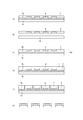
- Example 1 After forming the UV curable pressure-sensitive adhesive layer 2a on one side of the resin film 1a obtained in Production Example 4, this is cut into a circle having a diameter of 150 mm, and one end is cut to form an orientation flat.
- (A) 3a was produced [FIG. 1 (a)].
- two supports were used, two sheets having the same shape were produced. Hereinafter, they are represented as a support (A) 3a and a support (B) 3a, respectively.
- the semiconductor chip 4 On the UV curable pressure-sensitive adhesive layer of the support (A) 3a, the semiconductor chip 4 was arranged face-down on the basis of the orientation flat [FIG. 1 (b)].
- a semiconductor sealing epoxy resin is dropped on the support (A) 3a, compression molded at 120 ° C. for 10 minutes, and then at 150 ° C. for 60 minutes. Was cured to form a mold resin layer 5 to obtain a laminate (A) 6a [FIG. 1 (c)].
- slurry polishing treatment was performed on the mold resin layer of the laminate (A) 6a, washed with pure water, and then dried at 120 ° C. for 15 minutes [FIG. 2 (a)].
- the laminate (A) 6a was irradiated with 500 mJ / cm 2 of UV from the support (A) 3a side, and then the support (A) 3a was peeled off (FIG. 2 (b)).
- the support (B) 3a was attached to the polished surface of the mold resin layer 5 after the support (A) 3a was peeled off to obtain a laminate (B) 6b [FIG. 2 (c)].
- a photosensitive resist is applied to the exposed surface of the semiconductor chip 4 of the laminate (B) 6b by a spin coating method, heat-treated at 120 ° C. for 2 minutes, and then exposed to 300 mJ / cm 2 through a mask of a predetermined wiring pattern. Went. Next, after developing with a TMAH (tetramethylammonium hydroxide) aqueous solution (concentration 2.38%), washing and drying were performed. Next, sputtering treatment was performed using a Ti / Cu target to form a Ti / Cu thin film. Next, after removing the photosensitive resist with a stripping solution, washing treatment and drying treatment were performed.
- TMAH tetramethylammonium hydroxide
- photosensitive polyimide is applied to the surface by spin coating, heat-treated at 120 ° C. for 5 minutes, and then exposed at 500 mJ / cm 2 through a mask having a predetermined wiring pattern. Processed. Next, development processing was performed with a TMAH aqueous solution (concentration 2.38%) to form a predetermined pattern. Next, heat treatment was performed at 250 ° C. for 60 minutes to cure the photosensitive polyimide, and then a Cu pattern was formed by an electroless plating method, and unnecessary Cu was removed with an etching solution. Furthermore, the photosensitive polyimide was applied again on the surface of the laminate (B) 6b, and the same process was repeated to form a multilayer wiring pattern 7. Next, an electroless Ni plating process, an electroless Au plating process, and a solder plating process were performed on the predetermined pattern, bumps were formed, and a semiconductor package was manufactured [FIG. 2 (d)].
- Example 2 After the UV curable adhesive layer 12a is formed on one side of the resin film 11a obtained in Production Example 5, this is cut into a circle having a diameter of 200 mm, and one end is cut to form an orientation flat, 13a was produced (FIG. 3a). A semiconductor sealing epoxy resin was applied on the UV curable adhesive layer of the support 13a, and the semiconductor epoxy resin was cured at 150 ° C. for 60 minutes to form a mold resin layer 15a. Further, a semiconductor chip 14a with a copper post was disposed on the mold resin layer 15a with the orientation flat as a reference in a face-up orientation (FIG. 3C).
- a semiconductor sealing epoxy resin is dropped on the support 13a, compression molded at 120 ° C. for 10 minutes, and then at 150 ° C. for 60 minutes. Was cured to form a mold resin layer 15b to obtain a laminate 16a (FIG. 3D).
- slurry polishing treatment was performed on the mold resin layer 15b of the laminate 16a, washed with pure water, and then dried at 120 ° C. for 15 minutes (FIG. 3E).
- a photosensitive resist is applied to the exposed surface of the semiconductor chip 14a with a copper post of the laminated body 16a by a spin coat method, heat-treated at 120 ° C.
- Example 3 A UV curable adhesive layer was formed on one side of the resin film obtained in Production Example 6 and then cut into a square of 250 mm ⁇ 250 mm to prepare a support. A semiconductor chip was placed on the support, and a semiconductor package was fabricated using the same process as in Example 1.
- Example 1 A borosilicate glass having a thickness of 700 ⁇ m was cut into a circle having a diameter of 150 mm and polished until the thickness reached 300 ⁇ m. Next, a UV curable adhesive layer was formed on one side thereof, and a support (C) was produced. A semiconductor package was produced in the same manner as in Example 1 except that the support (C) was used instead of the support (A) and the support (B). In this manufacturing method, 1) borosilicate glass is expensive, 2) borosilicate glass is difficult to form and polish, and it is expensive, and 3) is supported after a semiconductor package is manufactured. There are problems such as the cost of body disposal.
Landscapes
- Engineering & Computer Science (AREA)
- Chemical & Material Sciences (AREA)
- Computer Hardware Design (AREA)
- Physics & Mathematics (AREA)
- Condensed Matter Physics & Semiconductors (AREA)
- General Physics & Mathematics (AREA)
- Manufacturing & Machinery (AREA)
- Microelectronics & Electronic Packaging (AREA)
- Power Engineering (AREA)
- Organic Chemistry (AREA)
- Chemical Kinetics & Catalysis (AREA)
- Laminated Bodies (AREA)
- Container, Conveyance, Adherence, Positioning, Of Wafer (AREA)
- Structures Or Materials For Encapsulating Or Coating Semiconductor Devices Or Solid State Devices (AREA)
- Adhesives Or Adhesive Processes (AREA)
- Mechanical Treatment Of Semiconductor (AREA)
- Encapsulation Of And Coatings For Semiconductor Or Solid State Devices (AREA)
- Dicing (AREA)
- Adhesive Tapes (AREA)
Abstract
La présente invention concerne : un support de fabrication de boîtiers de semi-conducteurs qui présente une durabilité supérieure dans divers procédés tels que le polissage, le chauffage, l'exposition/le développement, le placage et le traitement sous vide ; l'utilisation dudit support pour la fabrication de boîtiers de semi-conducteurs ; et un procédé de fabrication de boîtiers de semi-conducteurs. Ce support de fabrication de boîtiers de semi-conducteurs comporte une couche de base et une couche adhésive adjacente à la couche de base, la couche de base étant formée à partir d'un film de résine contenant une structure alicyclique.
Priority Applications (3)
| Application Number | Priority Date | Filing Date | Title |
|---|---|---|---|
| JP2018525063A JP6992751B2 (ja) | 2016-06-28 | 2017-06-19 | 半導体パッケージ製造用支持体、半導体パッケージ製造用支持体の使用、及び半導体パッケージの製造方法 |
| CN201780035525.0A CN109478520B (zh) | 2016-06-28 | 2017-06-19 | 半导体封装体制造用支承体、半导体封装体制造用支承体的使用及半导体封装体的制造方法 |
| US16/306,959 US10896827B2 (en) | 2016-06-28 | 2017-06-19 | Support for manufacturing semiconductor packages, use of support for manufacturing semiconductor packages, and method for manufacturing semiconductor packages |
Applications Claiming Priority (2)
| Application Number | Priority Date | Filing Date | Title |
|---|---|---|---|
| JP2016128055 | 2016-06-28 | ||
| JP2016-128055 | 2016-06-28 |
Publications (1)
| Publication Number | Publication Date |
|---|---|
| WO2018003565A1 true WO2018003565A1 (fr) | 2018-01-04 |
Family
ID=60786820
Family Applications (1)
| Application Number | Title | Priority Date | Filing Date |
|---|---|---|---|
| PCT/JP2017/022504 WO2018003565A1 (fr) | 2016-06-28 | 2017-06-19 | Support de fabrication de boîtiers de semi-conducteurs, son utilisation et procédé de fabrication de boîtiers de semi-conducteurs |
Country Status (5)
| Country | Link |
|---|---|
| US (1) | US10896827B2 (fr) |
| JP (1) | JP6992751B2 (fr) |
| CN (1) | CN109478520B (fr) |
| TW (1) | TWI745384B (fr) |
| WO (1) | WO2018003565A1 (fr) |
Cited By (3)
| Publication number | Priority date | Publication date | Assignee | Title |
|---|---|---|---|---|
| JP2020036007A (ja) * | 2018-08-23 | 2020-03-05 | 東レ株式会社 | フィルム、及びフィルムの製造方法 |
| JP2020038924A (ja) * | 2018-09-05 | 2020-03-12 | 日立化成株式会社 | 材料の選定方法及びパネルの製造方法 |
| JP2021077834A (ja) * | 2019-11-13 | 2021-05-20 | 三井化学東セロ株式会社 | 部品製造方法 |
Families Citing this family (2)
| Publication number | Priority date | Publication date | Assignee | Title |
|---|---|---|---|---|
| KR102216172B1 (ko) * | 2017-07-14 | 2021-02-15 | 주식회사 엘지화학 | 절연층 제조방법 및 반도체 패키지 제조방법 |
| US11807712B2 (en) * | 2018-03-28 | 2023-11-07 | Zeon Corporation | Hydrogenated norbornene ring-opened polymer, and method of producing the same |
Citations (6)
| Publication number | Priority date | Publication date | Assignee | Title |
|---|---|---|---|---|
| JP2001332647A (ja) * | 2000-05-24 | 2001-11-30 | Matsushita Electric Ind Co Ltd | 樹脂封止型半導体装置の製造方法 |
| JP2003291156A (ja) * | 2002-04-05 | 2003-10-14 | Dainippon Ink & Chem Inc | セルフ・アセンブル型微細構造を有する積層フィルムの製造方法およびそこで使用する組成物 |
| JP2010083939A (ja) * | 2008-09-30 | 2010-04-15 | Arakawa Chem Ind Co Ltd | 活性エネルギー線硬化型粘着剤組成物 |
| JP2012104757A (ja) * | 2010-11-12 | 2012-05-31 | Shinko Electric Ind Co Ltd | 半導体パッケージの製造方法 |
| JP2013168541A (ja) * | 2012-02-16 | 2013-08-29 | Fujitsu Ltd | 半導体装置の製造方法及び電子装置の製造方法 |
| WO2013175987A1 (fr) * | 2012-05-25 | 2013-11-28 | リンテック株式会社 | Feuille de découpage de puce |
Family Cites Families (13)
| Publication number | Priority date | Publication date | Assignee | Title |
|---|---|---|---|---|
| US6883938B1 (en) * | 1998-02-20 | 2005-04-26 | Nippon Zeon Co., Ltd. | Lighting equipment |
| JP4352620B2 (ja) | 2001-02-26 | 2009-10-28 | 日本ゼオン株式会社 | ノルボルネン系開環重合体水素化物の製造方法 |
| WO2005121841A1 (fr) * | 2004-06-11 | 2005-12-22 | Zeon Corporation | Corps feuilleté anti-réfléchissement et pièce optique |
| JP2007016102A (ja) | 2005-07-06 | 2007-01-25 | Nippon Zeon Co Ltd | 環状オレフィン系重合体組成物および成形材料 |
| CN101477956B (zh) * | 2008-01-04 | 2012-05-16 | 南茂科技股份有限公司 | 小片重新配置的封装结构及封装方法 |
| WO2009148716A2 (fr) * | 2008-06-02 | 2009-12-10 | 3M Innovative Properties Company | Composition encapsulante adhésive et dispositifs électroniques faits avec celle-ci |
| US20110133362A1 (en) * | 2008-08-28 | 2011-06-09 | Mitsui Chemicals, Inc. | Mold release film for manufacturing semiconductor resin package and semiconductor resin package manufacturing method using same |
| JP5685012B2 (ja) | 2010-06-29 | 2015-03-18 | 新光電気工業株式会社 | 半導体パッケージの製造方法 |
| KR20130101008A (ko) | 2010-09-07 | 2013-09-12 | 니폰 제온 가부시키가이샤 | 수지 조성물 및 그 성형체 |
| US9082825B2 (en) * | 2011-10-19 | 2015-07-14 | Panasonic Corporation | Manufacturing method for semiconductor package, semiconductor package, and semiconductor device |
| US9620413B2 (en) * | 2012-10-02 | 2017-04-11 | STATS ChipPAC Pte. Ltd. | Semiconductor device and method of using a standardized carrier in semiconductor packaging |
| JP2015126123A (ja) * | 2013-12-26 | 2015-07-06 | 日東電工株式会社 | 半導体パッケージの製造方法 |
| EP3214113B1 (fr) * | 2014-10-28 | 2019-11-20 | Zeon Corporation | Film de résine et procédé de production d'un film de résine |
-
2017
- 2017-06-19 JP JP2018525063A patent/JP6992751B2/ja active Active
- 2017-06-19 US US16/306,959 patent/US10896827B2/en active Active
- 2017-06-19 WO PCT/JP2017/022504 patent/WO2018003565A1/fr active Application Filing
- 2017-06-19 CN CN201780035525.0A patent/CN109478520B/zh active Active
- 2017-06-21 TW TW106120697A patent/TWI745384B/zh active
Patent Citations (6)
| Publication number | Priority date | Publication date | Assignee | Title |
|---|---|---|---|---|
| JP2001332647A (ja) * | 2000-05-24 | 2001-11-30 | Matsushita Electric Ind Co Ltd | 樹脂封止型半導体装置の製造方法 |
| JP2003291156A (ja) * | 2002-04-05 | 2003-10-14 | Dainippon Ink & Chem Inc | セルフ・アセンブル型微細構造を有する積層フィルムの製造方法およびそこで使用する組成物 |
| JP2010083939A (ja) * | 2008-09-30 | 2010-04-15 | Arakawa Chem Ind Co Ltd | 活性エネルギー線硬化型粘着剤組成物 |
| JP2012104757A (ja) * | 2010-11-12 | 2012-05-31 | Shinko Electric Ind Co Ltd | 半導体パッケージの製造方法 |
| JP2013168541A (ja) * | 2012-02-16 | 2013-08-29 | Fujitsu Ltd | 半導体装置の製造方法及び電子装置の製造方法 |
| WO2013175987A1 (fr) * | 2012-05-25 | 2013-11-28 | リンテック株式会社 | Feuille de découpage de puce |
Cited By (6)
| Publication number | Priority date | Publication date | Assignee | Title |
|---|---|---|---|---|
| JP2020036007A (ja) * | 2018-08-23 | 2020-03-05 | 東レ株式会社 | フィルム、及びフィルムの製造方法 |
| JP7400263B2 (ja) | 2018-08-23 | 2023-12-19 | 東レ株式会社 | フィルム、及びフィルムの製造方法 |
| JP2020038924A (ja) * | 2018-09-05 | 2020-03-12 | 日立化成株式会社 | 材料の選定方法及びパネルの製造方法 |
| JP7238301B2 (ja) | 2018-09-05 | 2023-03-14 | 株式会社レゾナック | 材料の選定方法及びパネルの製造方法 |
| JP2021077834A (ja) * | 2019-11-13 | 2021-05-20 | 三井化学東セロ株式会社 | 部品製造方法 |
| JP7393921B2 (ja) | 2019-11-13 | 2023-12-07 | 三井化学東セロ株式会社 | 部品製造方法 |
Also Published As
| Publication number | Publication date |
|---|---|
| TW201801209A (zh) | 2018-01-01 |
| JPWO2018003565A1 (ja) | 2019-04-18 |
| US20190148175A1 (en) | 2019-05-16 |
| US10896827B2 (en) | 2021-01-19 |
| CN109478520A (zh) | 2019-03-15 |
| TWI745384B (zh) | 2021-11-11 |
| CN109478520B (zh) | 2023-04-21 |
| JP6992751B2 (ja) | 2022-01-13 |
Similar Documents
| Publication | Publication Date | Title |
|---|---|---|
| WO2018003565A1 (fr) | Support de fabrication de boîtiers de semi-conducteurs, son utilisation et procédé de fabrication de boîtiers de semi-conducteurs | |
| KR102501433B1 (ko) | 대상물의 처리 방법, 가고정용 조성물, 반도체 장치 및 그의 제조 방법 | |
| US20060027322A1 (en) | Polarizing plate and process for producing the same | |
| JP6060479B2 (ja) | 基材の処理方法、半導体装置および仮固定用組成物 | |
| EP3125276A1 (fr) | Film de base pour feuille de découpage en dés, feuille de découpage en dés comportant ledit film de base, et procédé de fabrication dudit film de base | |
| JP2009025427A (ja) | 多層フィルム及び発光デバイス | |
| US20190202005A1 (en) | Method for manufacturing optical film | |
| CN108475143B (zh) | 薄膜触控传感器及其制作方法 | |
| WO2015076126A1 (fr) | Film de base de feuille de découpage en dés, feuille de découpage en dés contenant ledit film de base, et procédé de fabrication dudit film de base | |
| WO2017056662A1 (fr) | Procédé de traitement de pièce à usiner, composition de fixation temporaire, dispositif à semi-conducteur, et son procédé de fabrication | |
| JP5361092B2 (ja) | ダイシングシート用基材フィルムおよびダイシングシート | |
| KR102534645B1 (ko) | 광학 필름, 제조 방법 및 다층 필름 | |
| JP4897137B2 (ja) | 偏光板 | |
| JP2017134305A (ja) | 延伸フィルム、製造方法、偏光板及び表示装置 | |
| US11867873B2 (en) | Method for producing multilayer optical film | |
| JPWO2019026842A1 (ja) | 光学フィルム及びその製造方法 | |
| WO2006112304A1 (fr) | Plaque de polarisation et procede de production de celle-ci | |
| JP4367179B2 (ja) | 積層体の製造方法および積層体 | |
| CN111465878B (zh) | 偏振片保护膜、偏振片及显示装置 | |
| KR102175717B1 (ko) | 다이싱 다이 본딩 필름 | |
| TWI764981B (zh) | 接著劑組成物、附有接著劑的支持體、接著薄膜、層合體、其製造方法及電子零件的製造方法 | |
| JP2009126097A (ja) | 積層体 | |
| JP6926891B2 (ja) | 対象物の処理方法、仮固定用組成物、半導体装置およびその製造方法 | |
| WO2015076127A1 (fr) | Film de base de feuille de découpage en dés et procédé de fabrication de film de base | |
| JP2024034293A (ja) | フィルム、偏光子保護フィルム、及び有機エレクトロルミネッセンスディスプレイ |
Legal Events
| Date | Code | Title | Description |
|---|---|---|---|
| WWE | Wipo information: entry into national phase |
Ref document number: 2018525063 Country of ref document: JP |
|
| 121 | Ep: the epo has been informed by wipo that ep was designated in this application |
Ref document number: 17819924 Country of ref document: EP Kind code of ref document: A1 |
|
| NENP | Non-entry into the national phase |
Ref country code: DE |
|
| 122 | Ep: pct application non-entry in european phase |
Ref document number: 17819924 Country of ref document: EP Kind code of ref document: A1 |