WO2018003372A1 - 基板処理装置及び基板処理方法並びに記憶媒体 - Google Patents
基板処理装置及び基板処理方法並びに記憶媒体 Download PDFInfo
- Publication number
- WO2018003372A1 WO2018003372A1 PCT/JP2017/019980 JP2017019980W WO2018003372A1 WO 2018003372 A1 WO2018003372 A1 WO 2018003372A1 JP 2017019980 W JP2017019980 W JP 2017019980W WO 2018003372 A1 WO2018003372 A1 WO 2018003372A1
- Authority
- WO
- WIPO (PCT)
- Prior art keywords
- substrate
- wafer
- unit
- circumferential direction
- deformation
- Prior art date
- Legal status (The legal status is an assumption and is not a legal conclusion. Google has not performed a legal analysis and makes no representation as to the accuracy of the status listed.)
- Ceased
Links
Images






Classifications
-
- H—ELECTRICITY
- H10—SEMICONDUCTOR DEVICES; ELECTRIC SOLID-STATE DEVICES NOT OTHERWISE PROVIDED FOR
- H10P—GENERIC PROCESSES OR APPARATUS FOR THE MANUFACTURE OR TREATMENT OF DEVICES COVERED BY CLASS H10
- H10P72/00—Handling or holding of wafers, substrates or devices during manufacture or treatment thereof
- H10P72/04—Apparatus for manufacture or treatment
- H10P72/0431—Apparatus for thermal treatment
- H10P72/0432—Apparatus for thermal treatment mainly by conduction
-
- C—CHEMISTRY; METALLURGY
- C23—COATING METALLIC MATERIAL; COATING MATERIAL WITH METALLIC MATERIAL; CHEMICAL SURFACE TREATMENT; DIFFUSION TREATMENT OF METALLIC MATERIAL; COATING BY VACUUM EVAPORATION, BY SPUTTERING, BY ION IMPLANTATION OR BY CHEMICAL VAPOUR DEPOSITION, IN GENERAL; INHIBITING CORROSION OF METALLIC MATERIAL OR INCRUSTATION IN GENERAL
- C23C—COATING METALLIC MATERIAL; COATING MATERIAL WITH METALLIC MATERIAL; SURFACE TREATMENT OF METALLIC MATERIAL BY DIFFUSION INTO THE SURFACE, BY CHEMICAL CONVERSION OR SUBSTITUTION; COATING BY VACUUM EVAPORATION, BY SPUTTERING, BY ION IMPLANTATION OR BY CHEMICAL VAPOUR DEPOSITION, IN GENERAL
- C23C16/00—Chemical coating by decomposition of gaseous compounds, without leaving reaction products of surface material in the coating, i.e. chemical vapour deposition [CVD] processes
- C23C16/02—Pretreatment of the material to be coated
- C23C16/0209—Pretreatment of the material to be coated by heating
-
- C—CHEMISTRY; METALLURGY
- C23—COATING METALLIC MATERIAL; COATING MATERIAL WITH METALLIC MATERIAL; CHEMICAL SURFACE TREATMENT; DIFFUSION TREATMENT OF METALLIC MATERIAL; COATING BY VACUUM EVAPORATION, BY SPUTTERING, BY ION IMPLANTATION OR BY CHEMICAL VAPOUR DEPOSITION, IN GENERAL; INHIBITING CORROSION OF METALLIC MATERIAL OR INCRUSTATION IN GENERAL
- C23C—COATING METALLIC MATERIAL; COATING MATERIAL WITH METALLIC MATERIAL; SURFACE TREATMENT OF METALLIC MATERIAL BY DIFFUSION INTO THE SURFACE, BY CHEMICAL CONVERSION OR SUBSTITUTION; COATING BY VACUUM EVAPORATION, BY SPUTTERING, BY ION IMPLANTATION OR BY CHEMICAL VAPOUR DEPOSITION, IN GENERAL
- C23C16/00—Chemical coating by decomposition of gaseous compounds, without leaving reaction products of surface material in the coating, i.e. chemical vapour deposition [CVD] processes
- C23C16/44—Chemical coating by decomposition of gaseous compounds, without leaving reaction products of surface material in the coating, i.e. chemical vapour deposition [CVD] processes characterised by the method of coating
- C23C16/458—Chemical coating by decomposition of gaseous compounds, without leaving reaction products of surface material in the coating, i.e. chemical vapour deposition [CVD] processes characterised by the method of coating characterised by the method used for supporting substrates in the reaction chamber
- C23C16/4582—Rigid and flat substrates, e.g. plates or discs
- C23C16/4583—Rigid and flat substrates, e.g. plates or discs the substrate being supported substantially horizontally
- C23C16/4586—Elements in the interior of the support, e.g. electrodes, heating or cooling devices
-
- C—CHEMISTRY; METALLURGY
- C23—COATING METALLIC MATERIAL; COATING MATERIAL WITH METALLIC MATERIAL; CHEMICAL SURFACE TREATMENT; DIFFUSION TREATMENT OF METALLIC MATERIAL; COATING BY VACUUM EVAPORATION, BY SPUTTERING, BY ION IMPLANTATION OR BY CHEMICAL VAPOUR DEPOSITION, IN GENERAL; INHIBITING CORROSION OF METALLIC MATERIAL OR INCRUSTATION IN GENERAL
- C23C—COATING METALLIC MATERIAL; COATING MATERIAL WITH METALLIC MATERIAL; SURFACE TREATMENT OF METALLIC MATERIAL BY DIFFUSION INTO THE SURFACE, BY CHEMICAL CONVERSION OR SUBSTITUTION; COATING BY VACUUM EVAPORATION, BY SPUTTERING, BY ION IMPLANTATION OR BY CHEMICAL VAPOUR DEPOSITION, IN GENERAL
- C23C16/00—Chemical coating by decomposition of gaseous compounds, without leaving reaction products of surface material in the coating, i.e. chemical vapour deposition [CVD] processes
- C23C16/44—Chemical coating by decomposition of gaseous compounds, without leaving reaction products of surface material in the coating, i.e. chemical vapour deposition [CVD] processes characterised by the method of coating
- C23C16/46—Chemical coating by decomposition of gaseous compounds, without leaving reaction products of surface material in the coating, i.e. chemical vapour deposition [CVD] processes characterised by the method of coating characterised by the method used for heating the substrate
-
- C—CHEMISTRY; METALLURGY
- C23—COATING METALLIC MATERIAL; COATING MATERIAL WITH METALLIC MATERIAL; CHEMICAL SURFACE TREATMENT; DIFFUSION TREATMENT OF METALLIC MATERIAL; COATING BY VACUUM EVAPORATION, BY SPUTTERING, BY ION IMPLANTATION OR BY CHEMICAL VAPOUR DEPOSITION, IN GENERAL; INHIBITING CORROSION OF METALLIC MATERIAL OR INCRUSTATION IN GENERAL
- C23C—COATING METALLIC MATERIAL; COATING MATERIAL WITH METALLIC MATERIAL; SURFACE TREATMENT OF METALLIC MATERIAL BY DIFFUSION INTO THE SURFACE, BY CHEMICAL CONVERSION OR SUBSTITUTION; COATING BY VACUUM EVAPORATION, BY SPUTTERING, BY ION IMPLANTATION OR BY CHEMICAL VAPOUR DEPOSITION, IN GENERAL
- C23C16/00—Chemical coating by decomposition of gaseous compounds, without leaving reaction products of surface material in the coating, i.e. chemical vapour deposition [CVD] processes
- C23C16/44—Chemical coating by decomposition of gaseous compounds, without leaving reaction products of surface material in the coating, i.e. chemical vapour deposition [CVD] processes characterised by the method of coating
- C23C16/46—Chemical coating by decomposition of gaseous compounds, without leaving reaction products of surface material in the coating, i.e. chemical vapour deposition [CVD] processes characterised by the method of coating characterised by the method used for heating the substrate
- C23C16/463—Cooling of the substrate
-
- C—CHEMISTRY; METALLURGY
- C23—COATING METALLIC MATERIAL; COATING MATERIAL WITH METALLIC MATERIAL; CHEMICAL SURFACE TREATMENT; DIFFUSION TREATMENT OF METALLIC MATERIAL; COATING BY VACUUM EVAPORATION, BY SPUTTERING, BY ION IMPLANTATION OR BY CHEMICAL VAPOUR DEPOSITION, IN GENERAL; INHIBITING CORROSION OF METALLIC MATERIAL OR INCRUSTATION IN GENERAL
- C23C—COATING METALLIC MATERIAL; COATING MATERIAL WITH METALLIC MATERIAL; SURFACE TREATMENT OF METALLIC MATERIAL BY DIFFUSION INTO THE SURFACE, BY CHEMICAL CONVERSION OR SUBSTITUTION; COATING BY VACUUM EVAPORATION, BY SPUTTERING, BY ION IMPLANTATION OR BY CHEMICAL VAPOUR DEPOSITION, IN GENERAL
- C23C16/00—Chemical coating by decomposition of gaseous compounds, without leaving reaction products of surface material in the coating, i.e. chemical vapour deposition [CVD] processes
- C23C16/44—Chemical coating by decomposition of gaseous compounds, without leaving reaction products of surface material in the coating, i.e. chemical vapour deposition [CVD] processes characterised by the method of coating
- C23C16/52—Controlling or regulating the coating process
-
- H—ELECTRICITY
- H10—SEMICONDUCTOR DEVICES; ELECTRIC SOLID-STATE DEVICES NOT OTHERWISE PROVIDED FOR
- H10P—GENERIC PROCESSES OR APPARATUS FOR THE MANUFACTURE OR TREATMENT OF DEVICES COVERED BY CLASS H10
- H10P72/00—Handling or holding of wafers, substrates or devices during manufacture or treatment thereof
- H10P72/06—Apparatus for monitoring, sorting, marking, testing or measuring
- H10P72/0602—Temperature monitoring
-
- H—ELECTRICITY
- H10—SEMICONDUCTOR DEVICES; ELECTRIC SOLID-STATE DEVICES NOT OTHERWISE PROVIDED FOR
- H10P—GENERIC PROCESSES OR APPARATUS FOR THE MANUFACTURE OR TREATMENT OF DEVICES COVERED BY CLASS H10
- H10P72/00—Handling or holding of wafers, substrates or devices during manufacture or treatment thereof
- H10P72/06—Apparatus for monitoring, sorting, marking, testing or measuring
- H10P72/0606—Position monitoring, e.g. misposition detection or presence detection
-
- H—ELECTRICITY
- H10—SEMICONDUCTOR DEVICES; ELECTRIC SOLID-STATE DEVICES NOT OTHERWISE PROVIDED FOR
- H10P—GENERIC PROCESSES OR APPARATUS FOR THE MANUFACTURE OR TREATMENT OF DEVICES COVERED BY CLASS H10
- H10P72/00—Handling or holding of wafers, substrates or devices during manufacture or treatment thereof
- H10P72/06—Apparatus for monitoring, sorting, marking, testing or measuring
- H10P72/0612—Production flow monitoring, e.g. for increasing throughput
-
- H—ELECTRICITY
- H10—SEMICONDUCTOR DEVICES; ELECTRIC SOLID-STATE DEVICES NOT OTHERWISE PROVIDED FOR
- H10P—GENERIC PROCESSES OR APPARATUS FOR THE MANUFACTURE OR TREATMENT OF DEVICES COVERED BY CLASS H10
- H10P72/00—Handling or holding of wafers, substrates or devices during manufacture or treatment thereof
- H10P72/50—Handling or holding of wafers, substrates or devices during manufacture or treatment thereof for positioning, orientation or alignment
-
- H—ELECTRICITY
- H10—SEMICONDUCTOR DEVICES; ELECTRIC SOLID-STATE DEVICES NOT OTHERWISE PROVIDED FOR
- H10P—GENERIC PROCESSES OR APPARATUS FOR THE MANUFACTURE OR TREATMENT OF DEVICES COVERED BY CLASS H10
- H10P72/00—Handling or holding of wafers, substrates or devices during manufacture or treatment thereof
- H10P72/50—Handling or holding of wafers, substrates or devices during manufacture or treatment thereof for positioning, orientation or alignment
- H10P72/57—Mask-wafer alignment
-
- H—ELECTRICITY
- H10—SEMICONDUCTOR DEVICES; ELECTRIC SOLID-STATE DEVICES NOT OTHERWISE PROVIDED FOR
- H10P—GENERIC PROCESSES OR APPARATUS FOR THE MANUFACTURE OR TREATMENT OF DEVICES COVERED BY CLASS H10
- H10P74/00—Testing or measuring during manufacture or treatment of wafers, substrates or devices
- H10P74/20—Testing or measuring during manufacture or treatment of wafers, substrates or devices characterised by the properties tested or measured, e.g. structural or electrical properties
- H10P74/203—Structural properties, e.g. testing or measuring thicknesses, line widths, warpage, bond strengths or physical defects
-
- H—ELECTRICITY
- H10—SEMICONDUCTOR DEVICES; ELECTRIC SOLID-STATE DEVICES NOT OTHERWISE PROVIDED FOR
- H10P—GENERIC PROCESSES OR APPARATUS FOR THE MANUFACTURE OR TREATMENT OF DEVICES COVERED BY CLASS H10
- H10P76/00—Manufacture or treatment of masks on semiconductor bodies, e.g. by lithography or photolithography
-
- H—ELECTRICITY
- H10—SEMICONDUCTOR DEVICES; ELECTRIC SOLID-STATE DEVICES NOT OTHERWISE PROVIDED FOR
- H10P—GENERIC PROCESSES OR APPARATUS FOR THE MANUFACTURE OR TREATMENT OF DEVICES COVERED BY CLASS H10
- H10P95/00—Generic processes or apparatus for manufacture or treatments not covered by the other groups of this subclass
- H10P95/90—Thermal treatments, e.g. annealing or sintering
Definitions
- the present invention relates to a technique for placing a substrate on a placement portion and performing a heat treatment.
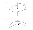
- the unique shape is a shape in which the height of the surface orthogonal to the central axis of the wafer differs in the circumferential direction, for example, a saddle shape, rather than the wafer deforming concentrically into a convex shape or a concave shape.
- the number of layers will be further increased, and the amount of deformation (warpage) of the wafer is expected to be larger than the current level. For this reason, the distance between the wafer and the mounting table surface is not uniform during the heat treatment, and the in-plane uniformity of the wafer temperature may be deteriorated.
- the heating module that performs the heat treatment is configured to divide the heated area of the wafer into a plurality of parts, and to provide a heater in each divided area, and to independently control the heat generation of each heater.
- each measured temperature when the temperature of the mounting table (hot plate) is measured at a plurality of measurement points is set to each target temperature.
- the heater is controlled.
- the heat of the heater is difficult to transfer to the wafer, it is difficult to reflect on the wafer temperature. Therefore, further improvement is necessary to perform heat treatment with good in-plane uniformity.
- the present invention has been made based on such circumstances, and an object thereof is to provide a technique capable of improving the uniformity of heat treatment in the plane of the substrate.
- the substrate processing apparatus of the present invention is In a substrate processing apparatus for placing a substrate on a placement unit and performing a heat treatment, In order to heat the substrate placed on the placement unit, a plurality of settings are set along the circumferential direction of the placement unit, and a heating control region that is independently temperature controlled, An adjustment unit that adjusts the relative orientation of the plurality of heating control regions in the circumferential direction with respect to the circumferential arrangement of the plurality of heating control regions, based on information related to the deformation of the substrate having different heights in the circumferential direction with respect to the plane orthogonal to the central axis of the substrate. And.
- the substrate processing method of the present invention comprises: Detecting the deformation of the substrate whose height relative to the plane orthogonal to the central axis of the substrate differs in the circumferential direction; A step of detecting deformation of the substrate by using a heating control region that is set in plural along the circumferential direction of the mounting unit and is independently temperature-controlled in order to heat the substrate mounted on the mounting unit. Adjusting the relative orientation of the substrate in the circumferential direction with respect to the circumferential arrangement of the plurality of heating control regions, based on the detection results obtained And heat-treating the substrate in a state where the relative direction of the circumferential direction of the substrate is adjusted.
- the storage medium of the present invention provides A storage medium storing a computer program used in a substrate processing apparatus that heats a substrate by placing the substrate on a mounting portion,
- the computer program includes a group of steps so as to implement the substrate processing method of the present invention.
- the substrate when a substrate is placed on a placement portion having a plurality of heating control regions that are set along the circumferential direction and each of which is temperature-controlled independently, the substrate is deformed. Based on this detection result, the relative direction of the circumferential direction of the substrate with respect to the circumferential arrangement of the plurality of heating control regions is adjusted. Therefore, even if the substrate is deformed so that the height relative to the plane orthogonal to the central axis differs in the circumferential direction, a region with a large deformation amount is placed on the boundary between the plurality of heating control regions. Is suppressed. For this reason, the temperature control of the heating control region is easily reflected in the substrate temperature, and the uniformity of the heat treatment in the substrate surface can be improved.
- substrate It is a block diagram which shows 1st Embodiment of a substrate processing apparatus. It is a vertical side view which shows the heating module provided in a substrate processing apparatus. It is a top view which shows the hot plate provided in a heating module. It is a longitudinal section which shows the detection module provided in a substrate processing apparatus. It is a block diagram which shows the control part provided in a substrate processing apparatus. It is a flowchart which shows the substrate processing method of 1st Embodiment. It is a characteristic view which shows the relationship between the position of the circumferential direction of a board
- FIG. 1 shows a wafer W without deformation (no warpage).
- the surface of the wafer W is a horizontal plane A orthogonal to the central axis C of the wafer W.
- 1B shows an example of the deformation, for example, showing a state of being deformed in a so-called bowl shape so that regions with a low height and regions with respect to the horizontal plane A are alternately arranged in the circumferential direction. Due to the multi-stacking of memory cells, there is an increasing tendency for the wafer W to be deformed into a bowl shape before the heat treatment.
- the substrate processing apparatus 1 of the present invention includes a heating module 11, a detection module 12, and a detection module 12 and a heating module 11 that place the wafer W on the mounting portion and perform heat treatment.
- the detection module 12 of this example serves as both an adjustment unit described later and a detection unit for detecting the circumferential deformation of the wafer W.
- the detection unit corresponds to an aspect of a deformation information acquisition unit that acquires information related to the deformation of the substrate.
- the transfer mechanism 13 is configured such that, for example, a holding member 131 that holds the back side of the wafer W can move up and down, move forward and backward, and move in the horizontal direction.
- FIG. 3 is a longitudinal side view showing an example of the heating module 11.
- the heating module 11 includes a housing 21, and 22 in the figure is a wafer W transfer port provided in the housing 21.
- reference numeral 23 denotes a horizontal hot plate whose surface is heated, which also serves as a mounting portion for the wafer W.
- a plurality of support pins 24 are provided on the surface of the hot plate 23, and the wafer W is placed on the support pins 24 and heated in a state of being slightly lifted from the surface of the hot plate 23.
- reference numeral 25 denotes a cooling plate for mounting and cooling the heated wafer W, and is horizontally placed between the standby position outside the hot plate 23 shown in FIG. And mediates the delivery between the transport mechanism 13 and the hot platen 23. Specifically, the transfer mechanism 13 moves up and down with respect to the cooling plate 25 at the standby position shown in FIG. 3, and the wafer W is transferred between the transfer mechanism 13 and the cooling plate 25. Further, when the cooling plate 25 moves to the upper side of the hot plate 23, the wafer W is transferred between them by cooperation of raising and lowering of an elevator pin (not shown) provided on the hot plate 23 and movement of the cooling plate 25.
- an elevator pin not shown
- FIG. 4 shows, as an example, a configuration in which heaters 31 to 35 are provided in five areas, and the areas in which the heaters 31 to 35 are provided correspond to the heating control areas H1 to H5.
- the surface of the hot plate 23 is set to be divided into five heating control regions H1 to H5, and heaters 31 to 35 are provided for each of the heating control regions H1 to H5.
- the temperature of H5 is configured to be controlled independently.
- the heaters 31 to 35 are shown in the same size as the heating control regions H1 to H5.
- the hot plate 23 is provided with temperature sensors 41 to 45 for detecting the temperatures of the heaters 31 to 35 and outputting detection signals for the respective heating control regions H1 to H5.
- the detection module 12 of this example serves both as an adjustment unit and a detection unit, and the adjustment unit is configured to detect a plurality of heating control regions H1 to H4 based on the detection result of the deformation of the wafer W.
- the direction of the circumferential direction of the wafer W with respect to the circumferential arrangement is adjusted.
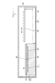
- the detection module 12 includes a housing 51, and 52 in the figure is a wafer W transfer port provided in the housing 51.
- 53 is a horizontal holding portion that holds the central portion of the back surface of the wafer W, and is formed smaller than the wafer W in plan view, for example.
- the holding unit 53 is connected to the rotation mechanism 54 via the rotation shaft 541 and is configured to be rotatable around the vertical axis while holding the wafer W.
- the holding unit 53 and the rotation mechanism 54 are mechanisms that adjust the orientation of the wafer W based on the detection result of the deformation of the wafer W before placing the wafer W on the hot plate (mounting unit) 23 of the heating module 11. is there.
- a plurality of support pins 531 are provided on the surface of the holding portion 53, and the wafer W is held in a state of being placed on the support pins 531, and the holding portion 53 is moved up and down and the transfer mechanism 13 is moved. In cooperation with each other, the wafer W is transferred between them.
- the holding unit 53 may be configured by a spin chuck that places the wafer W directly on the surface of the holding unit 53 and holds it by suction without providing the support pins 531.
- the detection module 12 the circumferential deformation of the wafer W is detected, for example, by measuring the distance from the wafer W in a direction orthogonal to the wafer W along the circumferential direction of the wafer W. Is a distance measuring unit. Therefore, the detection module 12 includes a distance sensor 55 including a laser displacement meter that detects the distance to the measurement target using laser light, and emits laser light to the peripheral edge of the back surface of the wafer W held by the holding unit 53. It is configured to output. Then, the distance L between the distance sensor 55 and the wafer W in the direction orthogonal to the wafer W is measured by measuring the distance to the wafer W by the distance sensor 55 while rotating the holding unit 53 that holds the wafer W. Measured along the circumferential direction.
- the detection module 12 the measurement result of the circumferential distance in the peripheral region of the wafer W is acquired as the deformation detection result. Based on this detection result, the plurality of heating control regions H1 to H4 in the heating module 11 are obtained. The orientation of the wafer W in the circumferential direction with respect to the circumferential arrangement is adjusted. Specifically, the detection result of the deformation by the distance sensor 55 is output to the control unit 14, and the control unit 14 controls the control signal for adjusting the circumferential direction of the wafer W based on the detection result, the heating A control signal for adjusting the temperature of each of the heaters 31 to 35 in the control region H1 to H5 is output.
- the control unit 14 includes a CPU 62, a memory (storage unit) 63, an input unit 64, a direction adjustment unit 65, and a temperature adjustment unit 66 connected to the bus 61.
- a distance sensor 55 and temperature sensors 41 to 45 are connected to the bus 61, respectively.
- the CPU 62 performs various calculations for executing a heat treatment process flow to be described later.
- the input unit 64 includes a mouse, a keyboard, a touch panel, and the like, and is provided so that a user of the apparatus can perform various operations in order to advance the flow of the heat treatment process.
- Each of the direction adjustment unit 65 and the temperature adjustment unit 66 is configured by a computer program, for example, and has a group of steps so that a flow described later can be executed.
- This program is installed in the control unit 14 from a storage medium such as a hard disk, a compact disk, a magneto-optical disk, a memory card, or a flexible disk.
- the wafer W is loaded into the detection module 12 and placed on the holding unit 53.
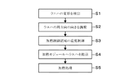
- the distance L to the wafer W in the direction orthogonal to the wafer W is measured by the distance sensor 55 along the circumferential direction of the wafer W, and the deformation of the wafer W and the position of the wafer W ( The position of the notch N) is detected, and the detection result is output to the control unit 14 (step S1).
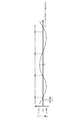
- FIG. 8 schematically shows the detection result of the deformation of the wafer W.
- the horizontal axis indicates the circumferential position of the wafer W
- the vertical axis indicates the distance L from the wafer W as the deformation amount.
- L0 on the vertical axis is the distance to the horizontal plane A (see FIG. 1, the surface of the wafer without warping), and a distance larger than the distance L0 warps upward in a direction away from the hot plate 23.
- Lmax is the maximum deformation amount (warpage amount) when warped upward.
- a distance smaller than the distance L0 indicates a state of warping downward in a direction approaching the hot plate 23, and Lmin is a maximum deformation amount when warping downward.
- the waveform is interrupted, and the notch position is grasped by the position where the waveform is interrupted.
- the maximum value of the deformation amount of the wafer W is Lmax as an example.
- control unit 14 Based on the detection result, the control unit 14 outputs a control signal for adjusting the circumferential direction of the wafer W by the direction adjustment unit 65 to the detection module 12 (step S2), and at the temperature adjustment unit 66. Control signals for adjusting the temperatures of the heaters 31 to 35 in the heating control regions H1 to H5 are output to the heating module 11 (step 3).
- the orientation adjusting unit 65 adjusts the orientation of the wafer W so that the maximum portion of the wafer deformation is not disposed at the boundary between the heating control regions H1 to H4 adjacent in the circumferential direction, for example.
- the wafer W whose deformation has been detected by the detection module 12 is transferred to the heating module 11 by the transfer mechanism 13.
- the wafer W is transferred to the hot plate 23 so that the center line B and the notch N are aligned.
- the center line B of the hot plate 23 is, for example, a line connecting the center position in the circumferential direction of a certain heating control region (H1 in this example) and the center 231 of the hot plate 23.
- the detection module 12 prevents the position P1 having the maximum deformation amount from reaching the boundary between the heating control regions based on the detection result shown in FIG. Adjust the orientation.
- the rotation mechanism 54 is rotated counterclockwise by an angle ⁇ so that the circumferential position P1 is aligned with the center line B (see FIG. 9B).
- the wafer W after the orientation adjustment is transferred by the transfer mechanism 13 onto the hot plate 23 of the heating module 11 so that the circumferential position P1 is aligned with the circumferential center of the heating control region H3, for example. (See FIG. 9C).
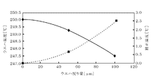
- FIG. 10 shows an example of the relationship between the warp amount (deformation amount) of the wafer W and the wafer temperature during heat treatment.
- the horizontal axis is the amount of warpage of the wafer W
- the left vertical axis is the wafer temperature during the heat treatment
- the right vertical axis is the correction temperature
- ⁇ is the wafer temperature plot
- ⁇ is the correction temperature plot.
- the warpage amount of the wafer W in FIG. 10 refers to the wafer surface (horizontal plane A in FIG.
- the wafer W When the wafer W is warped upward, it is separated from the hot plate 23, so that it is difficult to transfer heat from the hot plate 23.
- the temperature of the hot plate 23 When the temperature of the hot plate 23 is the same, the temperature of the wafer W is lower than when the wafer W is not warped. Become.
- the inventor has grasped that there is a correlation between the amount of warpage of the wafer W and the wafer temperature during the heat treatment. By obtaining this correlation in advance, the wafer temperature during the heat treatment is obtained from the amount of warpage of the wafer W, and the correction temperature is obtained based on this. Correlation data between the amount of wafer warpage and the correction temperature is acquired in advance by performing an evaluation test.
- the wafer temperature when the warp amount is 0 is the target temperature (250 ° C.)
- the wafer temperature when the warp amount is 100 ⁇ m is 247.5 ° C., and therefore the temperature corresponding to the difference from the target temperature is 2.5.
- the temperature control of the heating control region H3 is performed by adding the correction temperature to the set temperature of the heater 33. Further, the heaters 31 to 35 in the heating control regions H1 to H5 are controlled so as to reach the set temperature based on the detection values of the temperature sensors 41 to 45.
- the temperature control of the heater 33 is performed by adding or subtracting the correction temperature obtained from the warpage amount to the correction value of the temperature based on the detection value of the temperature sensor 43.
- temperature control is performed so that the heaters 31, 32, 34, and 35 become set temperatures based on detection values of the temperature sensors 41, 42, 44, and 45, for example. I do.
- the wafer W whose orientation is adjusted in the detection module 12 is transferred to the heating module 11 by the transfer mechanism 13 and transferred to the hot plate 23 (step S4).
- the wafer W is placed on the hot plate 23 such that the circumferential position P ⁇ b> 1 is aligned with the center line B of the hot plate 23.
- the heat treatment of the wafer W is started in a state where the temperature control of each of the heating control regions H1 to H5 is completed (step S5).
- the wafer W that has been heat-treated for a predetermined time in this manner is transferred to the transfer mechanism 13 via the cooling plate 25 and transferred from the heating module 11 to another module (not shown).
- the wafer W is rotated in the circumferential direction of the wafer W relative to the circumferential arrangement of the heating control regions H1 to H4 of the hot plate 23. It is adjusted. Therefore, even if the wafer W is deformed in a unique shape such that the height relative to the plane orthogonal to the central axis differs in the circumferential direction, the region having a large deformation amount in the wafer W has a plurality of heating control regions H1 to H4. It is possible to prevent the wafers from being placed on the boundary between each other and improve the uniformity of the heat treatment in the wafer surface.
- the heaters 31 to 34 are not embedded at the boundary between the heating control regions, heat transfer to the wafer is difficult compared to the region where the heater is embedded. For this reason, if a portion with a large deformation amount of the wafer W is arranged at the boundary between the heating control regions, the temperature of the portion of the wafer W becomes lower than that of other regions, and the in-plane uniformity of the wafer temperature. Will get worse. Therefore, if a region with a large amount of deformation as in the present invention is arranged at a position away from the boundary between the heating control regions, the temperature control of the heating control region is easily reflected in the wafer temperature, and the uniformity of the heating process within the wafer surface. Can be improved.
- the position P1 where the deformation amount is large in the wafer is arranged in the central region in the circumferential direction of the heating control region H3, and the temperature control of the heating control region H3 is performed based on the deformation amount of the wafer W.
- appropriate heating control can be performed in accordance with the deformation amount of the wafer W.
- good uniformity of heat treatment is ensured in the wafer surface.
- the case where the maximum deformation amount of the wafer W is Lmax has been described as an example. However, since the wafer W is placed on the support pins 24, the wafer W warps downward in a direction approaching the hot plate 23. There is also. For example, the case where the maximum deformation amount of the wafer W is Lmin based on the detection result of FIG. 8 will be described. In this case, since the heat plate 23 comes closer to the hot plate 23 than the wafer W having no warpage, heat transfer from the hot plate 23 is facilitated, and when the temperature of the hot plate 23 is the same, the wafer W is not warped. The temperature rises.
- the wafer temperature is obtained from the warpage amount of the wafer W, and the difference temperature between the wafer temperature and the target temperature of the wafer W is calculated.
- the correction temperature for example, the temperature control is performed by subtracting it from the set temperature of the heater 33.
- the wafer W is oriented so that the position P1 of the maximum deformation amount is aligned with the center line B, and the wafer W is divided into four peripheral regions S1 to S4 so as to correspond to the heating control regions H1 to H4. Then, the temperature of each heating control region H1 to H4 may be controlled based on the deformation amount (warpage amount) of the peripheral region S1 to S4 of the wafer W.
- the maximum value of the deformation amount is obtained, and the correction temperature is obtained based on the maximum value, and the temperature of the heating control areas H1 to H4 is adjusted by adjusting to the set temperature of the heaters 31 to 34.
- the heating control regions H1 to H4 are temperature-controlled over a wide range of the wafer W in accordance with the amount of deformation, even better in-plane uniformity is ensured for the wafer temperature during heat treatment. be able to.
- the temperature of the heating control region does not necessarily need to be controlled based on the deformation amount of the corresponding wafer W. For example, when the wafer W is deformed into a bowl shape, the lower portion and the higher portion appear alternately from each other as described above, so the deformation amount of the wafer W is evaluated in advance, The first heating control region whose temperature is controlled to be higher and the second heating control region whose temperature is controlled to be lower than the set temperature are alternately set.
- FIGS. 1 and 2 a second embodiment of the substrate processing apparatus of the present invention will be described with reference to FIGS.
- This embodiment is different from the first embodiment in that the alignment of the heating control regions is adjusted instead of adjusting the orientation of the wafer W based on the detection result of the deformation of the wafer W.
- an adjustment part is comprised by the mechanism in which the arrangement
- heaters 71 to 79 each having a heating mechanism are embedded in different regions as viewed in plan.
- the heating module 11 includes a switch unit that selects a combination of heaters from a plurality of heaters.
- a switch unit 81 that selects a combination (71 and 72) and (71 and 78) of two adjacent heaters from among the three heaters 71, 72, and 78 adjacent to each other, and three adjacent to each other.
- a switch unit 82 for selecting a combination (72 and 73) of two adjacent heaters from among the heaters 72, 73, and 74, and (73 and 74). Further, a switch unit 83 for selecting a combination (74 and 75) of two adjacent heaters from among the three heaters 74, 75 and 76 adjacent to each other, (75 and 76), and three heaters 76 adjacent to each other, 77 and 78, a combination of two adjacent heaters (76 and 77), and a switch section 84 for selecting (77 and 78).
- Reference numerals 85, 86, 87, and 88 denote power supply units.
- These switch units 81 to 84 are configured to be switched between the first combination and the second combination by a control signal from the control unit 14.
- the first combination is to select a combination of heaters (71 and 78), heaters (72 and 73), heaters (74 and 75), heaters (76 and 77), and the second combination is a heater ( 71 and 72), heaters (73 and 74), heaters (75 and 76), and combinations of heaters (77 and 78) are selected.
- the heating control region H11 that combines the heating zones Z1 and Z8, the heating control region H12 that combines the heating zones Z2 and Z3, and the heating zones Z4 and Z5. Is set, and a heating control region H14 is set that combines the heating zones Z6 and Z7.
- the heating control region H11 that combines the heating zones Z1 and Z2 the heating control region H12 that combines the heating zones Z3 and Z4, and the heating zones Z5 and Z6.
- the heating control region H14 is set by combining the heating zones Z7 and Z8.
- the heating control region H15 is set in the central region by the heating zone Z9.
- the heating plate 7 includes, for example, between the heating zone Z1 and the heating zone Z2, between the heating zone Z3 and the heating zone Z4, between the heating zone Z5 and the heating zone Z6, and between the heating zone Z7 and the heating zone Z8.
- temperature sensors 91 to 95 are provided in the heating zone Z9.
- the temperature sensor 91 is a heating control area H11
- the temperature sensor 92 is a heating control area H12
- the temperature sensor 93 is a heating control area H13
- the temperature sensor 94 is a heating control area H14
- the temperature sensor 95 is a temperature control area H15. It is provided to do.
- the adjustment unit of this example includes a plurality of heaters 71 to 78 and switch units 81 to 84 for selecting a combination of heaters corresponding to the heating control regions H11 to H14 from the plurality of heaters 71 to 78. These correspond to a mechanism for adjusting the circumferential arrangement of the heating control regions H11 to H14 based on the detection result of the deformation of the wafer W.
- the control part 14 is provided with the arrangement
- the alignment adjusting unit is configured to output a control signal for adjusting the alignment in the circumferential direction of the four heating control regions H11 to H14 to the heating module 11 based on the detection result of the deformation of the wafer W.
- the detection module 12 functions as a detection unit and a distance measurement unit
- the heating module 11 functions as an adjustment unit.
- Other configurations are the same as those of the first embodiment, and the same components are denoted by the same reference numerals and description thereof is omitted.
- the wafer W is carried into the detection module 12 and placed on the holding unit 53, and the deformation of the wafer W and the notch position of the wafer W are detected by the distance sensor 55 as described above (step S11).
- the control unit 14 outputs a control signal for selecting the combination of the heaters 71 to 78 to the heating module 11 based on the detection result (step S12), and the temperature adjustment unit 66 outputs the control signal to the heating module 11.
- a control signal for adjusting the temperature of each of the heaters 71 to 79 in each of the heating control regions H1 to H5 is output (step 13).
- the combination of heaters is set so that the circumferential position P ⁇ b> 1 having the maximum deformation amount (Lmax in this case) does not reach the boundary between the heating control regions. Either the first combination or the second combination is selected, and the switch sections 81 to 84 are switched. For example, in this example, a combination of heaters whose position P1 is closer to the center line of the heating control region to be arranged is selected.
- the warpage amount (Lmax ⁇ L0) of the wafer W is based on the correlation data between the warpage amount of the wafer and the wafer temperature.
- the temperature control of the heaters 71 and 72 is performed by adding the correction temperature obtained from the warpage amount to the temperature correction value based on the detection value of the temperature sensor 91.
- temperature control is performed so that the heaters 73 to 79 are set to the set temperature based on the temperature correction values based on the detection values of the temperature sensors 92 to 95.
- two heaters provided in the same heating control region are controlled to have the same temperature by the corresponding temperature sensors 91 to 94.
- the wafer W is transferred from the detection module 12 to the heating module 11 by the transfer mechanism 13 and transferred to the hot plate 7 (step S14). Thereafter, for example, the heat treatment of the wafer W is started in a state where the temperature control of each of the heating control regions H11 to H15 is performed (step S15). Thereafter, the wafer W that has been heat-treated for a predetermined time is transferred from the heating module 11 to another module (not shown) by the transfer mechanism 13.
- the wafer W with respect to the heating control regions H11 to H14 is adjusted.
- the relative direction of the circumferential direction is adjusted. Therefore, as in the first embodiment, even when the wafer W is deformed and the distance between the wafer and the hot plate surface is not uniform, a region with a large deformation amount in the wafer W is not heated. Mounting on the boundary between the control regions H11 to H14 is suppressed, and the uniformity of the heat treatment within the wafer surface can be improved.
- the temperature is controlled by the correction temperature obtained based on the deformation amount (warpage amount) of the peripheral region of the corresponding wafer W. Good in-plane uniformity can be secured for the wafer temperature during the heat treatment.
- the coating / developing apparatus 100 includes a carrier block D1, a processing block D2, an interface block D3, and an exposure apparatus D4.
- the wafer W is taken out from the carrier 102 mounted on the mounting table 101 of the carrier block D1.
- the processing block D2 includes two unit blocks E1, E2, and E3 stacked on each other.
- the unit block E1 is a block for applying a chemical solution for forming an antireflection film on the wafer W and heating the wafer W after the chemical solution is applied.
- Each of the blocks D1 to D3 is provided with a wafer W transfer mechanism, and the wafer W in the carrier 102 is transferred from the carrier block D1, the unit block E1, the unit block E2, the interface block D3, the exposure apparatus D4, and the interface block D3.
- Each unit is transported in the order of the unit block E3 and the above processes are performed.
- the wafer W on which the resist pattern is formed is transferred to the carrier block D1 and returned to the carrier 102.
- FIG. 15 is a plan view showing the unit block E3.
- a plurality of modules are arranged in a shelf shape on the left and right sides of the transfer path 103 of the wafer W extending in the front-rear direction.
- a number of the heating modules 11 of the present invention for performing PEB are provided on the shelf.
- the detection module 12 is provided.
- a developing module 104 for supplying a developing solution to the wafer W is provided on the left and right sides of the transport path 103.
- reference numeral 13 denotes a transfer mechanism for transferring the wafer W among the developing module 104, the heating module 11, the detection module 12, and the interface block D3.
- the exposed wafer W is loaded into the processing block D2 via the transfer arm 105 and the transfer module 106 of the interface block D3. Then, after being transported to the detection module 12 by the transport mechanism 13 and the deformation of the wafer W is detected, it is transported to one of the multiple heating modules 11.
- the unit block E2 of the coating and developing apparatus 100 is configured to include the detection module 12 and the heating module 11 like the unit block E3, except that a resist coating module is provided instead of the development module 104. May be.
- the relative orientation of the wafer W and the heating control region is adjusted based on the detection result.
- the wafer W is transferred to the heating module 11 and subjected to a heat treatment, and the applied resist is dried to form a resist film.
- a resist film can be formed with high uniformity within the surface of the wafer W, and CD uniformity can be improved within the surface of the wafer W. Can do.
- the unit block E1 may be configured similarly to the unit block E3 except that a chemical application module for forming an antireflection film is provided instead of the developing module 104. Also in this case, the detection module 12 detects the deformation of the wafer W, the relative orientation of the wafer W and the heating control area is adjusted based on the detection result, and then the wafer W is transported to the heating module 11 and is predetermined. The heat treatment is performed.
- the substrate processing apparatus of the present invention does not necessarily have to include a detection unit for detecting deformation of a substrate whose height with respect to a plane orthogonal to the central axis of the substrate differs in the circumferential direction.
- the detection unit is provided in an apparatus different from the substrate processing apparatus, and the relative direction in the circumferential direction of the substrate and the heating control region is adjusted by the adjustment unit using the detection result of the deformation of the substrate detected by the detection unit. May be adjusted.
- a control unit provided in the substrate processing apparatus obtains information on the deformation of the substrate sent from outside the substrate processing apparatus online, and based on this information, for example, the transport mechanism 13 or the heating control A control signal is output to an adjustment mechanism for adjusting the arrangement of the regions.
- the information regarding the deformation of the substrate sent from outside the substrate processing apparatus is sent from, for example, a detection unit that detects the deformation of the substrate, from another device that includes the detection unit, or from a host computer.
- the control unit corresponds to a deformation information acquisition unit that acquires information related to the deformation of the substrate.
- the detection module illustrated in FIG. 5 is configured not to include a distance sensor, and the detection module is oriented to the substrate. It is provided as an adjustment unit that adjusts. In the second embodiment, it is not necessary to provide the detection module shown in FIG.
- the detection unit is not limited to the configuration shown in FIG. 5.
- a distance sensor that measures the distance from the substrate in a direction orthogonal to the substrate and is movable in the horizontal direction relative to the substrate is provided above the substrate.
- the structure to provide may be sufficient.
- the distance to the substrate is measured not only in the peripheral region of the substrate but also in the central region of the substrate.
- the temperature may be controlled by obtaining a correction temperature in the heating control region.
- the amount of warpage is not limited to the above example, and may be acquired based on the distance between the surface of the hot plate 23 and the wafer W. For example, in FIG.
- the distance L and Lmin (the lowest height position of the wafer) ) And the difference may be obtained.
- the present invention can be applied to a configuration in which the wafer is directly placed on the surface of the hot plate, instead of placing the wafer on the hot plate via the support pins.
- a plurality of wafers are stored in a carrier and loaded into the substrate processing apparatus. For example, the deformation information acquired for the first wafer of a lot that forms a wafer group as a carrier unit is used as a subsequent wafer included in the lot. May apply.
- Heating module 12 Detection module 13 Transport mechanism 14 Control unit 23, 7 Heat plates 31-35, 71-79 Heater 41 to 45, 91 to 95 Temperature sensors H1 to H5, H11 to H15 Heating control zone Z1 to Z9 Heating zone 100 Coating and developing device
Landscapes
- Chemical & Material Sciences (AREA)
- Engineering & Computer Science (AREA)
- General Chemical & Material Sciences (AREA)
- Chemical Kinetics & Catalysis (AREA)
- Materials Engineering (AREA)
- Mechanical Engineering (AREA)
- Metallurgy (AREA)
- Organic Chemistry (AREA)
- Exposure Of Semiconductors, Excluding Electron Or Ion Beam Exposure (AREA)
- Container, Conveyance, Adherence, Positioning, Of Wafer (AREA)
- Automation & Control Theory (AREA)
- Testing Or Measuring Of Semiconductors Or The Like (AREA)
Abstract
Description
基板を載置部に載置して加熱処理する基板処理装置において、
前記載置部に載置された基板を加熱するために載置部の周方向に沿って複数設定され、各々独立して温度制御される加熱制御領域と、
基板の中心軸と直交する面に対する高さが周方向で異なる基板の変形に関する情報に基づいて、前記複数の加熱制御領域の周方向の並びに対する基板の周方向の相対的向きを調整する調整部と、を備えたことを特徴とする。
基板の中心軸と直交する面に対する高さが周方向で異なる基板の変形を検出する工程と、
載置部に載置された基板を加熱するために載置部の周方向に沿って複数設定され、各々独立して温度制御される加熱制御領域を用い、前記基板の変形を検出する工程にて得られた検出結果に基づいて、前記複数の加熱制御領域の周方向の並びに対する基板の周方向の相対的向きを調整する工程と、
前記基板の周方向の相対的向きが調整された状態で基板を加熱処理する工程と、を含むことを特徴とする。
基板を載置部に載置して加熱処理する基板処理装置に用いられるコンピュータプログラムを記憶した記憶媒体であって、
前記コンピュータプログラムは、本発明の基板処理方法を実施するようにステップ群が組まれていることを特徴とする。
本発明の基板処理装置の第1の実施形態について、図1~図10を参照しながら説明する。本発明の基板処理の対象となるウエハWは、図1に示すように、ウエハWの中心軸と直交する面に対する高さが周方向で異なる形状に変形したものである。図1(a)は変形のない(反りのない)ウエハWを示しており、例えばこのウエハWの表面を、ウエハWの中心軸Cと直交する水平面Aとする。図1(b)は変形の一例であり、例えば水平面Aに対する高さが低い領域と高い領域とが周方向に交互に並ぶように、言わば鞍型形状に変形した状態を示している。メモリセルの多積層化により、ウエハWが加熱処理の前に鞍型形状に変形する例が増加傾向にある。
搬送機構13は、例えばウエハWの裏面側を保持する保持部材131が昇降自在、進退自在、水平方向に移動自在に構成されている。
(第2の実施形態)
このように検出部を基板処理装置とは別の装置に設けた場合には、第1の実施形態では、図5に示す検出モジュールは距離センサを設けない構成とし、当該検出モジュールは基板の向きを調整する調整部として設けられる。また、第2の実施形態では、図5に示す検出モジュールを設ける必要はない。
なお、ウエハは、キャリアに複数枚収納されて基板処理装置に搬入されるが、例えばキャリア単位であるウエハ群をなすロットの先頭のウエハについて取得した変形情報を、当該ロットに含まれる後続のウエハについて適用してもよい。
11 加熱モジュール
12 検出モジュール
13 搬送機構
14 制御部
23、7 熱板
31~35、71~79 ヒータ
41~45、91~95 温度センサ
H1~H5、H11~H15 加熱制御領域
Z1~Z9 加熱ゾーン
100 塗布、現像装置
Claims (13)
- 基板を載置部に載置して加熱処理する基板処理装置において、
前記載置部に載置された基板を加熱するために載置部の周方向に沿って複数設定され、各々独立して温度制御される加熱制御領域と、
基板の中心軸と直交する面に対する高さが周方向で異なる基板の変形に関する情報に基づいて、前記複数の加熱制御領域の周方向の並びに対する基板の周方向の相対的向きを調整する調整部と、を備えたことを特徴とする基板処理装置。 - 前記基板の変形に関する情報を取得する変形情報取得部を備えたことを特徴とする請求項1記載の基板処理装置。
- 前記変形情報取得部は、前記基板の変形を検出するための検出部であることを特徴とする請求項2記載の基板処理装置。
- 前記載置部は、周方向に配置された複数のヒータにより加熱される熱板を兼用することを特徴とする請求項1記載の基板処理装置。
- 前記調整部は、基板を載置部に載置する前に、前記基板の変形に関する情報に基づいて当該基板の向きを調整する機構であることを特徴とする請求項1記載の基板処理装置。
- 前記調整部は、前記基板の変形に関する情報に基づいて前記複数の加熱制御領域の周方向の並びを調整する機構であることを特徴とする請求項1記載の基板処理装置。
- 前記調整部は、載置部の周方向に沿って配置された複数の加熱機構と、前記複数の加熱機構の中から各加熱制御領域に対応する加熱機構の組み合わせを選択するスイッチ部と、を含むことを特徴とする請求項6記載の基板処理装置。
- 前記情報は、基板と直交する方向における基板との距離を基板の周方向に沿って測定する距離測定部にて測定された測定結果であることを特徴とする請求項1記載の基板処理装置。
- 前記基板の周方向の変形を検出するための検出部と、
前記検出部の検出結果に基づいて前記基板の周方向の相対的向きを調整するための制御信号を出力する制御部と、を備えたことを特徴とする請求項1記載の基板処理装置。 - 基板の中心軸と直交する面に対する高さが周方向で異なる基板の変形を検出する工程と、
載置部に載置された基板を加熱するために載置部の周方向に沿って複数設定され、各々独立して温度制御される加熱制御領域を用い、前記基板の変形を検出する工程にて得られた検出結果に基づいて、前記複数の加熱制御領域の周方向の並びに対する基板の周方向の相対的向きを調整する工程と、
前記基板の周方向の相対的向きが調整された状態で基板を加熱処理する工程と、を含むことを特徴とする基板処理方法。 - 前記基板の周方向の相対的向きを調整する工程は、基板を載置部に載置する前に、前記検出結果に基づいて当該基板の向きを調整する工程であることを特徴とする請求項10記載の基板処理方法。
- 前記基板の周方向の相対的向きを調整する工程は、前記検出結果に基づいて前記複数の加熱制御領域の周方向の並びを調整する工程であることを特徴とする請求項10記載の基板処理方法。
- 基板を載置部に載置して加熱処理する基板処理装置に用いられるコンピュータプログラムを記憶した記憶媒体であって、
前記コンピュータプログラムは、請求項10に記載の基板処理方法を実施するようにステップ群が組まれていることを特徴とする記憶媒体。
Priority Applications (4)
| Application Number | Priority Date | Filing Date | Title |
|---|---|---|---|
| CN201780040255.2A CN109417024B (zh) | 2016-06-27 | 2017-05-30 | 基板处理装置、基板处理方法以及存储介质 |
| JP2018524968A JP6690711B2 (ja) | 2016-06-27 | 2017-05-30 | 基板処理装置及び基板処理方法並びに記憶媒体 |
| US16/313,268 US11142823B2 (en) | 2016-06-27 | 2017-05-30 | Substrate processing apparatus, substrate processing method, and storage medium |
| KR1020187037786A KR102304247B1 (ko) | 2016-06-27 | 2017-05-30 | 기판 처리 장치 및 기판 처리 방법 및 기억 매체 |
Applications Claiming Priority (2)
| Application Number | Priority Date | Filing Date | Title |
|---|---|---|---|
| JP2016-126300 | 2016-06-27 | ||
| JP2016126300 | 2016-06-27 |
Publications (1)
| Publication Number | Publication Date |
|---|---|
| WO2018003372A1 true WO2018003372A1 (ja) | 2018-01-04 |
Family
ID=60786989
Family Applications (1)
| Application Number | Title | Priority Date | Filing Date |
|---|---|---|---|
| PCT/JP2017/019980 Ceased WO2018003372A1 (ja) | 2016-06-27 | 2017-05-30 | 基板処理装置及び基板処理方法並びに記憶媒体 |
Country Status (6)
| Country | Link |
|---|---|
| US (1) | US11142823B2 (ja) |
| JP (1) | JP6690711B2 (ja) |
| KR (1) | KR102304247B1 (ja) |
| CN (1) | CN109417024B (ja) |
| TW (1) | TWI794177B (ja) |
| WO (1) | WO2018003372A1 (ja) |
Cited By (3)
| Publication number | Priority date | Publication date | Assignee | Title |
|---|---|---|---|---|
| JP2019186498A (ja) * | 2018-04-17 | 2019-10-24 | 東京エレクトロン株式会社 | 基板処理装置、基板処理方法、及び記憶媒体 |
| US20220344575A1 (en) * | 2021-04-27 | 2022-10-27 | Taiwan Semiconductor Manufacturing Co., Ltd. | Voltage breakdown uniformity in piezoelectric structure for piezoelectric devices |
| US11587807B2 (en) * | 2018-10-28 | 2023-02-21 | Taiwan Semiconductor Manufacturing Co., Ltd. | Annealing apparatus and method thereof |
Families Citing this family (9)
| Publication number | Priority date | Publication date | Assignee | Title |
|---|---|---|---|---|
| JP7312020B2 (ja) * | 2019-05-30 | 2023-07-20 | 株式会社Screenホールディングス | 熱処理方法および熱処理装置 |
| JP7292115B2 (ja) * | 2019-06-07 | 2023-06-16 | 東京エレクトロン株式会社 | 温度調整装置及び温度制御方法。 |
| CN112420591B (zh) * | 2019-08-20 | 2022-06-10 | 长鑫存储技术有限公司 | 加热板及控制晶圆表面温度的方法 |
| CN110752171B (zh) * | 2019-11-01 | 2022-07-29 | 长江存储科技有限责任公司 | 晶圆弯曲度调整装置及方法 |
| JP7432354B2 (ja) * | 2019-12-19 | 2024-02-16 | 東京エレクトロン株式会社 | 熱処理装置 |
| CN111415887A (zh) * | 2020-03-27 | 2020-07-14 | 宁波润华全芯微电子设备有限公司 | 一种晶圆加热装置 |
| CN113960884B (zh) * | 2020-07-21 | 2024-05-14 | 长鑫存储技术有限公司 | 温度调控系统及温度调控方法 |
| CN114678286A (zh) * | 2020-12-25 | 2022-06-28 | 中国科学院微电子研究所 | 晶圆变形的测量方法 |
| CN115910866B (zh) * | 2022-12-07 | 2026-04-28 | 西安奕斯伟材料科技股份有限公司 | 一种外延晶圆的生产控制方法和装置 |
Citations (9)
| Publication number | Priority date | Publication date | Assignee | Title |
|---|---|---|---|---|
| JP2001274069A (ja) * | 2000-03-27 | 2001-10-05 | Toshiba Corp | レジストパターン形成方法及び半導体製造システム |
| JP2006228820A (ja) * | 2005-02-15 | 2006-08-31 | Tokyo Electron Ltd | 熱処理板の温度設定方法,熱処理板の温度設定装置,プログラム及びプログラムを記録したコンピュータ読み取り可能な記録媒体 |
| JP2006237260A (ja) * | 2005-02-24 | 2006-09-07 | Tokyo Electron Ltd | 基板の処理システム,プログラム及びプログラムを記録したコンピュータ読み取り可能な記録媒体 |
| JP2006324335A (ja) * | 2005-05-17 | 2006-11-30 | Dainippon Screen Mfg Co Ltd | 熱処理装置 |
| JP2007317732A (ja) * | 2006-05-23 | 2007-12-06 | Tokyo Electron Ltd | 熱処理板の温度制御方法、プログラム及び熱処理板の温度制御装置 |
| JP2008053464A (ja) * | 2006-08-24 | 2008-03-06 | Tokyo Electron Ltd | 塗布、現像装置、レジストパターン形成装置、塗布、現像方法、レジストパターンの形成方法及び記憶媒体。 |
| JP2008177303A (ja) * | 2007-01-17 | 2008-07-31 | Tokyo Electron Ltd | 基板処理装置、基板処理方法及び記憶媒体 |
| JP2009200388A (ja) * | 2008-02-25 | 2009-09-03 | Tokyo Electron Ltd | 基板の処理方法、プログラム、コンピュータ記憶媒体及び基板処理システム |
| JP2013207030A (ja) * | 2012-03-28 | 2013-10-07 | Elpida Memory Inc | レジスト塗布処理装置およびレジスト塗布処理方法 |
Family Cites Families (5)
| Publication number | Priority date | Publication date | Assignee | Title |
|---|---|---|---|---|
| JP2008066295A (ja) * | 2006-08-08 | 2008-03-21 | Sumitomo Electric Ind Ltd | 発熱体回路パターン、それを搭載したサセプタ及び半導体製造装置 |
| JP4391518B2 (ja) | 2006-12-28 | 2009-12-24 | 東京エレクトロン株式会社 | 温度制御方法、調整装置、温度調節器、プログラム、記録媒体および加熱処理装置 |
| JP5358956B2 (ja) * | 2008-01-19 | 2013-12-04 | 東京エレクトロン株式会社 | 載置台装置、処理装置、温度制御方法及び記憶媒体 |
| JP2013046047A (ja) * | 2011-08-26 | 2013-03-04 | Toshiba Corp | 加熱装置および半導体装置の製造方法 |
| US10049905B2 (en) * | 2014-09-25 | 2018-08-14 | Tokyo Electron Limited | Substrate heat treatment apparatus, substrate heat treatment method, storage medium and heat-treatment-condition detecting apparatus |
-
2017
- 2017-05-30 KR KR1020187037786A patent/KR102304247B1/ko active Active
- 2017-05-30 CN CN201780040255.2A patent/CN109417024B/zh active Active
- 2017-05-30 JP JP2018524968A patent/JP6690711B2/ja active Active
- 2017-05-30 WO PCT/JP2017/019980 patent/WO2018003372A1/ja not_active Ceased
- 2017-05-30 US US16/313,268 patent/US11142823B2/en active Active
- 2017-06-16 TW TW106120077A patent/TWI794177B/zh active
Patent Citations (9)
| Publication number | Priority date | Publication date | Assignee | Title |
|---|---|---|---|---|
| JP2001274069A (ja) * | 2000-03-27 | 2001-10-05 | Toshiba Corp | レジストパターン形成方法及び半導体製造システム |
| JP2006228820A (ja) * | 2005-02-15 | 2006-08-31 | Tokyo Electron Ltd | 熱処理板の温度設定方法,熱処理板の温度設定装置,プログラム及びプログラムを記録したコンピュータ読み取り可能な記録媒体 |
| JP2006237260A (ja) * | 2005-02-24 | 2006-09-07 | Tokyo Electron Ltd | 基板の処理システム,プログラム及びプログラムを記録したコンピュータ読み取り可能な記録媒体 |
| JP2006324335A (ja) * | 2005-05-17 | 2006-11-30 | Dainippon Screen Mfg Co Ltd | 熱処理装置 |
| JP2007317732A (ja) * | 2006-05-23 | 2007-12-06 | Tokyo Electron Ltd | 熱処理板の温度制御方法、プログラム及び熱処理板の温度制御装置 |
| JP2008053464A (ja) * | 2006-08-24 | 2008-03-06 | Tokyo Electron Ltd | 塗布、現像装置、レジストパターン形成装置、塗布、現像方法、レジストパターンの形成方法及び記憶媒体。 |
| JP2008177303A (ja) * | 2007-01-17 | 2008-07-31 | Tokyo Electron Ltd | 基板処理装置、基板処理方法及び記憶媒体 |
| JP2009200388A (ja) * | 2008-02-25 | 2009-09-03 | Tokyo Electron Ltd | 基板の処理方法、プログラム、コンピュータ記憶媒体及び基板処理システム |
| JP2013207030A (ja) * | 2012-03-28 | 2013-10-07 | Elpida Memory Inc | レジスト塗布処理装置およびレジスト塗布処理方法 |
Cited By (7)
| Publication number | Priority date | Publication date | Assignee | Title |
|---|---|---|---|---|
| JP2019186498A (ja) * | 2018-04-17 | 2019-10-24 | 東京エレクトロン株式会社 | 基板処理装置、基板処理方法、及び記憶媒体 |
| JP6994424B2 (ja) | 2018-04-17 | 2022-01-14 | 東京エレクトロン株式会社 | 基板処理装置、基板処理方法、及び記憶媒体 |
| US11587807B2 (en) * | 2018-10-28 | 2023-02-21 | Taiwan Semiconductor Manufacturing Co., Ltd. | Annealing apparatus and method thereof |
| US12266553B2 (en) | 2018-10-28 | 2025-04-01 | Taiwan Semiconductor Manufacturing Co., Ltd. | Annealing method |
| US20220344575A1 (en) * | 2021-04-27 | 2022-10-27 | Taiwan Semiconductor Manufacturing Co., Ltd. | Voltage breakdown uniformity in piezoelectric structure for piezoelectric devices |
| US11832520B2 (en) * | 2021-04-27 | 2023-11-28 | Taiwan Semiconductor Manufacturing Company, Ltd. | Voltage breakdown uniformity in piezoelectric structure for piezoelectric devices |
| US12615963B2 (en) | 2021-04-27 | 2026-04-28 | Taiwan Semiconductor Manufacturing Company, Ltd. | Semiconductor substrate processing tool with hot plate chamber |
Also Published As
| Publication number | Publication date |
|---|---|
| JP6690711B2 (ja) | 2020-04-28 |
| CN109417024A (zh) | 2019-03-01 |
| TWI794177B (zh) | 2023-03-01 |
| US11142823B2 (en) | 2021-10-12 |
| CN109417024B (zh) | 2023-07-28 |
| KR102304247B1 (ko) | 2021-09-17 |
| US20190153602A1 (en) | 2019-05-23 |
| TW201810373A (zh) | 2018-03-16 |
| JPWO2018003372A1 (ja) | 2019-04-11 |
| KR20190021267A (ko) | 2019-03-05 |
Similar Documents
| Publication | Publication Date | Title |
|---|---|---|
| JP6690711B2 (ja) | 基板処理装置及び基板処理方法並びに記憶媒体 | |
| US8242417B2 (en) | Temperature control method of heat processing plate, computer storage medium, and temperature control apparatus of heat processing plate | |
| US7902485B2 (en) | Temperature setting method of thermal processing plate, temperature setting apparatus of thermal processing plate, program, and computer-readable recording medium recording program thereon | |
| US8138456B2 (en) | Heat processing method, computer-readable storage medium, and heat processing apparatus | |
| WO2008023693A1 (fr) | Machine de développement de revêtement, dispositif de formation de motif de réserve, procédé de développement de revêtement, procédé de formation de motif de réserve, et support de stockage | |
| US8041525B2 (en) | Substrate measuring method, computer-readable recording medium recording program thereon, and substrate measuring system | |
| JP2006228820A (ja) | 熱処理板の温度設定方法,熱処理板の温度設定装置,プログラム及びプログラムを記録したコンピュータ読み取り可能な記録媒体 | |
| JP2020136397A (ja) | 基板処理装置及び基板処理方法 | |
| KR101072282B1 (ko) | 기판 처리 장치, 기판 처리 방법, 기판 처리 프로그램 및 그 프로그램을 기록한 컴퓨터 판독 가능한 기록 매체 | |
| JP2009021443A (ja) | 基板処理装置及び基板処理方法 | |
| JP2025020390A (ja) | 半導体デバイスの製造システム及び製造方法 | |
| JP2006222354A (ja) | 熱処理板の温度設定方法,熱処理板の温度設定装置,プログラム及びプログラムを記録したコンピュータ読み取り可能な記録媒体 | |
| JP2007110080A (ja) | 基板処理装置、基板処理方法、基板処理プログラム、及びそのプログラムを記録したコンピュータ読み取り可能な記録媒体 | |
| JP4920317B2 (ja) | 基板の処理方法、プログラム、コンピュータ読み取り可能な記録媒体及び基板の処理システム | |
| JP6196173B2 (ja) | 基板処理システム、基板処理方法、プログラム及びコンピュータ記憶媒体 | |
| JP2009245996A (ja) | 基板の処理方法、プログラム、コンピュータ記憶媒体及び基板処理システム | |
| WO2011099221A1 (ja) | 基板処理方法 |
Legal Events
| Date | Code | Title | Description |
|---|---|---|---|
| 121 | Ep: the epo has been informed by wipo that ep was designated in this application |
Ref document number: 17819739 Country of ref document: EP Kind code of ref document: A1 |
|
| ENP | Entry into the national phase |
Ref document number: 2018524968 Country of ref document: JP Kind code of ref document: A |
|
| ENP | Entry into the national phase |
Ref document number: 20187037786 Country of ref document: KR Kind code of ref document: A |
|
| NENP | Non-entry into the national phase |
Ref country code: DE |
|
| 122 | Ep: pct application non-entry in european phase |
Ref document number: 17819739 Country of ref document: EP Kind code of ref document: A1 |