WO2017195620A1 - 光源装置及び照明装置 - Google Patents
光源装置及び照明装置 Download PDFInfo
- Publication number
- WO2017195620A1 WO2017195620A1 PCT/JP2017/016707 JP2017016707W WO2017195620A1 WO 2017195620 A1 WO2017195620 A1 WO 2017195620A1 JP 2017016707 W JP2017016707 W JP 2017016707W WO 2017195620 A1 WO2017195620 A1 WO 2017195620A1
- Authority
- WO
- WIPO (PCT)
- Prior art keywords
- wavelength conversion
- light
- conversion unit
- source device
- light source
- Prior art date
Links
Images


Classifications
-
- F—MECHANICAL ENGINEERING; LIGHTING; HEATING; WEAPONS; BLASTING
- F21—LIGHTING
- F21S—NON-PORTABLE LIGHTING DEVICES; SYSTEMS THEREOF; VEHICLE LIGHTING DEVICES SPECIALLY ADAPTED FOR VEHICLE EXTERIORS
- F21S41/00—Illuminating devices specially adapted for vehicle exteriors, e.g. headlamps
- F21S41/10—Illuminating devices specially adapted for vehicle exteriors, e.g. headlamps characterised by the light source
- F21S41/14—Illuminating devices specially adapted for vehicle exteriors, e.g. headlamps characterised by the light source characterised by the type of light source
- F21S41/16—Laser light sources
-
- F—MECHANICAL ENGINEERING; LIGHTING; HEATING; WEAPONS; BLASTING
- F21—LIGHTING
- F21S—NON-PORTABLE LIGHTING DEVICES; SYSTEMS THEREOF; VEHICLE LIGHTING DEVICES SPECIALLY ADAPTED FOR VEHICLE EXTERIORS
- F21S41/00—Illuminating devices specially adapted for vehicle exteriors, e.g. headlamps
- F21S41/10—Illuminating devices specially adapted for vehicle exteriors, e.g. headlamps characterised by the light source
- F21S41/14—Illuminating devices specially adapted for vehicle exteriors, e.g. headlamps characterised by the light source characterised by the type of light source
- F21S41/176—Light sources where the light is generated by photoluminescent material spaced from a primary light generating element
-
- F—MECHANICAL ENGINEERING; LIGHTING; HEATING; WEAPONS; BLASTING
- F21—LIGHTING
- F21S—NON-PORTABLE LIGHTING DEVICES; SYSTEMS THEREOF; VEHICLE LIGHTING DEVICES SPECIALLY ADAPTED FOR VEHICLE EXTERIORS
- F21S41/00—Illuminating devices specially adapted for vehicle exteriors, e.g. headlamps
- F21S41/10—Illuminating devices specially adapted for vehicle exteriors, e.g. headlamps characterised by the light source
- F21S41/19—Attachment of light sources or lamp holders
- F21S41/192—Details of lamp holders, terminals or connectors
-
- F—MECHANICAL ENGINEERING; LIGHTING; HEATING; WEAPONS; BLASTING
- F21—LIGHTING
- F21S—NON-PORTABLE LIGHTING DEVICES; SYSTEMS THEREOF; VEHICLE LIGHTING DEVICES SPECIALLY ADAPTED FOR VEHICLE EXTERIORS
- F21S41/00—Illuminating devices specially adapted for vehicle exteriors, e.g. headlamps
- F21S41/20—Illuminating devices specially adapted for vehicle exteriors, e.g. headlamps characterised by refractors, transparent cover plates, light guides or filters
- F21S41/25—Projection lenses
-
- F—MECHANICAL ENGINEERING; LIGHTING; HEATING; WEAPONS; BLASTING
- F21—LIGHTING
- F21S—NON-PORTABLE LIGHTING DEVICES; SYSTEMS THEREOF; VEHICLE LIGHTING DEVICES SPECIALLY ADAPTED FOR VEHICLE EXTERIORS
- F21S41/00—Illuminating devices specially adapted for vehicle exteriors, e.g. headlamps
- F21S41/20—Illuminating devices specially adapted for vehicle exteriors, e.g. headlamps characterised by refractors, transparent cover plates, light guides or filters
- F21S41/285—Refractors, transparent cover plates, light guides or filters not provided in groups F21S41/24-F21S41/28
-
- F—MECHANICAL ENGINEERING; LIGHTING; HEATING; WEAPONS; BLASTING
- F21—LIGHTING
- F21S—NON-PORTABLE LIGHTING DEVICES; SYSTEMS THEREOF; VEHICLE LIGHTING DEVICES SPECIALLY ADAPTED FOR VEHICLE EXTERIORS
- F21S41/00—Illuminating devices specially adapted for vehicle exteriors, e.g. headlamps
- F21S41/30—Illuminating devices specially adapted for vehicle exteriors, e.g. headlamps characterised by reflectors
- F21S41/32—Optical layout thereof
- F21S41/321—Optical layout thereof the reflector being a surface of revolution or a planar surface, e.g. truncated
-
- F—MECHANICAL ENGINEERING; LIGHTING; HEATING; WEAPONS; BLASTING
- F21—LIGHTING
- F21S—NON-PORTABLE LIGHTING DEVICES; SYSTEMS THEREOF; VEHICLE LIGHTING DEVICES SPECIALLY ADAPTED FOR VEHICLE EXTERIORS
- F21S41/00—Illuminating devices specially adapted for vehicle exteriors, e.g. headlamps
- F21S41/30—Illuminating devices specially adapted for vehicle exteriors, e.g. headlamps characterised by reflectors
- F21S41/32—Optical layout thereof
- F21S41/36—Combinations of two or more separate reflectors
- F21S41/365—Combinations of two or more separate reflectors successively reflecting the light
-
- F—MECHANICAL ENGINEERING; LIGHTING; HEATING; WEAPONS; BLASTING
- F21—LIGHTING
- F21S—NON-PORTABLE LIGHTING DEVICES; SYSTEMS THEREOF; VEHICLE LIGHTING DEVICES SPECIALLY ADAPTED FOR VEHICLE EXTERIORS
- F21S41/00—Illuminating devices specially adapted for vehicle exteriors, e.g. headlamps
- F21S41/30—Illuminating devices specially adapted for vehicle exteriors, e.g. headlamps characterised by reflectors
- F21S41/39—Attachment thereof
-
- F—MECHANICAL ENGINEERING; LIGHTING; HEATING; WEAPONS; BLASTING
- F21—LIGHTING
- F21S—NON-PORTABLE LIGHTING DEVICES; SYSTEMS THEREOF; VEHICLE LIGHTING DEVICES SPECIALLY ADAPTED FOR VEHICLE EXTERIORS
- F21S45/00—Arrangements within vehicle lighting devices specially adapted for vehicle exteriors, for purposes other than emission or distribution of light
- F21S45/70—Prevention of harmful light leakage
-
- F—MECHANICAL ENGINEERING; LIGHTING; HEATING; WEAPONS; BLASTING
- F21—LIGHTING
- F21V—FUNCTIONAL FEATURES OR DETAILS OF LIGHTING DEVICES OR SYSTEMS THEREOF; STRUCTURAL COMBINATIONS OF LIGHTING DEVICES WITH OTHER ARTICLES, NOT OTHERWISE PROVIDED FOR
- F21V13/00—Producing particular characteristics or distribution of the light emitted by means of a combination of elements specified in two or more of main groups F21V1/00 - F21V11/00
- F21V13/12—Combinations of only three kinds of elements
- F21V13/14—Combinations of only three kinds of elements the elements being filters or photoluminescent elements, reflectors and refractors
-
- F—MECHANICAL ENGINEERING; LIGHTING; HEATING; WEAPONS; BLASTING
- F21—LIGHTING
- F21V—FUNCTIONAL FEATURES OR DETAILS OF LIGHTING DEVICES OR SYSTEMS THEREOF; STRUCTURAL COMBINATIONS OF LIGHTING DEVICES WITH OTHER ARTICLES, NOT OTHERWISE PROVIDED FOR
- F21V7/00—Reflectors for light sources
- F21V7/22—Reflectors for light sources characterised by materials, surface treatments or coatings, e.g. dichroic reflectors
- F21V7/24—Reflectors for light sources characterised by materials, surface treatments or coatings, e.g. dichroic reflectors characterised by the material
-
- F—MECHANICAL ENGINEERING; LIGHTING; HEATING; WEAPONS; BLASTING
- F21—LIGHTING
- F21V—FUNCTIONAL FEATURES OR DETAILS OF LIGHTING DEVICES OR SYSTEMS THEREOF; STRUCTURAL COMBINATIONS OF LIGHTING DEVICES WITH OTHER ARTICLES, NOT OTHERWISE PROVIDED FOR
- F21V9/00—Elements for modifying spectral properties, polarisation or intensity of the light emitted, e.g. filters
- F21V9/30—Elements containing photoluminescent material distinct from or spaced from the light source
- F21V9/32—Elements containing photoluminescent material distinct from or spaced from the light source characterised by the arrangement of the photoluminescent material
-
- F—MECHANICAL ENGINEERING; LIGHTING; HEATING; WEAPONS; BLASTING
- F21—LIGHTING
- F21V—FUNCTIONAL FEATURES OR DETAILS OF LIGHTING DEVICES OR SYSTEMS THEREOF; STRUCTURAL COMBINATIONS OF LIGHTING DEVICES WITH OTHER ARTICLES, NOT OTHERWISE PROVIDED FOR
- F21V9/00—Elements for modifying spectral properties, polarisation or intensity of the light emitted, e.g. filters
- F21V9/30—Elements containing photoluminescent material distinct from or spaced from the light source
- F21V9/38—Combination of two or more photoluminescent elements of different materials
-
- F—MECHANICAL ENGINEERING; LIGHTING; HEATING; WEAPONS; BLASTING
- F21—LIGHTING
- F21V—FUNCTIONAL FEATURES OR DETAILS OF LIGHTING DEVICES OR SYSTEMS THEREOF; STRUCTURAL COMBINATIONS OF LIGHTING DEVICES WITH OTHER ARTICLES, NOT OTHERWISE PROVIDED FOR
- F21V9/00—Elements for modifying spectral properties, polarisation or intensity of the light emitted, e.g. filters
- F21V9/40—Elements for modifying spectral properties, polarisation or intensity of the light emitted, e.g. filters with provision for controlling spectral properties, e.g. colour, or intensity
- F21V9/45—Elements for modifying spectral properties, polarisation or intensity of the light emitted, e.g. filters with provision for controlling spectral properties, e.g. colour, or intensity by adjustment of photoluminescent elements
-
- G—PHYSICS
- G02—OPTICS
- G02B—OPTICAL ELEMENTS, SYSTEMS OR APPARATUS
- G02B27/00—Optical systems or apparatus not provided for by any of the groups G02B1/00 - G02B26/00, G02B30/00
- G02B27/10—Beam splitting or combining systems
- G02B27/1006—Beam splitting or combining systems for splitting or combining different wavelengths
-
- G—PHYSICS
- G02—OPTICS
- G02B—OPTICAL ELEMENTS, SYSTEMS OR APPARATUS
- G02B5/00—Optical elements other than lenses
- G02B5/02—Diffusing elements; Afocal elements
- G02B5/0205—Diffusing elements; Afocal elements characterised by the diffusing properties
-
- H—ELECTRICITY
- H01—ELECTRIC ELEMENTS
- H01L—SEMICONDUCTOR DEVICES NOT COVERED BY CLASS H10
- H01L33/00—Semiconductor devices with at least one potential-jump barrier or surface barrier specially adapted for light emission; Processes or apparatus specially adapted for the manufacture or treatment thereof or of parts thereof; Details thereof
- H01L33/48—Semiconductor devices with at least one potential-jump barrier or surface barrier specially adapted for light emission; Processes or apparatus specially adapted for the manufacture or treatment thereof or of parts thereof; Details thereof characterised by the semiconductor body packages
- H01L33/50—Wavelength conversion elements
- H01L33/501—Wavelength conversion elements characterised by the materials, e.g. binder
- H01L33/502—Wavelength conversion materials
-
- H—ELECTRICITY
- H01—ELECTRIC ELEMENTS
- H01S—DEVICES USING THE PROCESS OF LIGHT AMPLIFICATION BY STIMULATED EMISSION OF RADIATION [LASER] TO AMPLIFY OR GENERATE LIGHT; DEVICES USING STIMULATED EMISSION OF ELECTROMAGNETIC RADIATION IN WAVE RANGES OTHER THAN OPTICAL
- H01S5/00—Semiconductor lasers
- H01S5/005—Optical components external to the laser cavity, specially adapted therefor, e.g. for homogenisation or merging of the beams or for manipulating laser pulses, e.g. pulse shaping
- H01S5/0087—Optical components external to the laser cavity, specially adapted therefor, e.g. for homogenisation or merging of the beams or for manipulating laser pulses, e.g. pulse shaping for illuminating phosphorescent or fluorescent materials, e.g. using optical arrangements specifically adapted for guiding or shaping laser beams illuminating these materials
-
- H—ELECTRICITY
- H01—ELECTRIC ELEMENTS
- H01S—DEVICES USING THE PROCESS OF LIGHT AMPLIFICATION BY STIMULATED EMISSION OF RADIATION [LASER] TO AMPLIFY OR GENERATE LIGHT; DEVICES USING STIMULATED EMISSION OF ELECTROMAGNETIC RADIATION IN WAVE RANGES OTHER THAN OPTICAL
- H01S5/00—Semiconductor lasers
- H01S5/02—Structural details or components not essential to laser action
- H01S5/022—Mountings; Housings
- H01S5/023—Mount members, e.g. sub-mount members
- H01S5/02325—Mechanically integrated components on mount members or optical micro-benches
- H01S5/02326—Arrangements for relative positioning of laser diodes and optical components, e.g. grooves in the mount to fix optical fibres or lenses
-
- F—MECHANICAL ENGINEERING; LIGHTING; HEATING; WEAPONS; BLASTING
- F21—LIGHTING
- F21Y—INDEXING SCHEME ASSOCIATED WITH SUBCLASSES F21K, F21L, F21S and F21V, RELATING TO THE FORM OR THE KIND OF THE LIGHT SOURCES OR OF THE COLOUR OF THE LIGHT EMITTED
- F21Y2115/00—Light-generating elements of semiconductor light sources
- F21Y2115/30—Semiconductor lasers
-
- H—ELECTRICITY
- H01—ELECTRIC ELEMENTS
- H01S—DEVICES USING THE PROCESS OF LIGHT AMPLIFICATION BY STIMULATED EMISSION OF RADIATION [LASER] TO AMPLIFY OR GENERATE LIGHT; DEVICES USING STIMULATED EMISSION OF ELECTROMAGNETIC RADIATION IN WAVE RANGES OTHER THAN OPTICAL
- H01S5/00—Semiconductor lasers
- H01S5/02—Structural details or components not essential to laser action
- H01S5/022—Mountings; Housings
- H01S5/0225—Out-coupling of light
- H01S5/02251—Out-coupling of light using optical fibres
-
- H—ELECTRICITY
- H01—ELECTRIC ELEMENTS
- H01S—DEVICES USING THE PROCESS OF LIGHT AMPLIFICATION BY STIMULATED EMISSION OF RADIATION [LASER] TO AMPLIFY OR GENERATE LIGHT; DEVICES USING STIMULATED EMISSION OF ELECTROMAGNETIC RADIATION IN WAVE RANGES OTHER THAN OPTICAL
- H01S5/00—Semiconductor lasers
- H01S5/02—Structural details or components not essential to laser action
- H01S5/022—Mountings; Housings
- H01S5/0225—Out-coupling of light
- H01S5/02255—Out-coupling of light using beam deflecting elements
-
- H—ELECTRICITY
- H01—ELECTRIC ELEMENTS
- H01S—DEVICES USING THE PROCESS OF LIGHT AMPLIFICATION BY STIMULATED EMISSION OF RADIATION [LASER] TO AMPLIFY OR GENERATE LIGHT; DEVICES USING STIMULATED EMISSION OF ELECTROMAGNETIC RADIATION IN WAVE RANGES OTHER THAN OPTICAL
- H01S5/00—Semiconductor lasers
- H01S5/02—Structural details or components not essential to laser action
- H01S5/024—Arrangements for thermal management
- H01S5/02469—Passive cooling, e.g. where heat is removed by the housing as a whole or by a heat pipe without any active cooling element like a TEC
-
- H—ELECTRICITY
- H01—ELECTRIC ELEMENTS
- H01S—DEVICES USING THE PROCESS OF LIGHT AMPLIFICATION BY STIMULATED EMISSION OF RADIATION [LASER] TO AMPLIFY OR GENERATE LIGHT; DEVICES USING STIMULATED EMISSION OF ELECTROMAGNETIC RADIATION IN WAVE RANGES OTHER THAN OPTICAL
- H01S5/00—Semiconductor lasers
- H01S5/06—Arrangements for controlling the laser output parameters, e.g. by operating on the active medium
- H01S5/068—Stabilisation of laser output parameters
- H01S5/06825—Protecting the laser, e.g. during switch-on/off, detection of malfunctioning or degradation
-
- H—ELECTRICITY
- H01—ELECTRIC ELEMENTS
- H01S—DEVICES USING THE PROCESS OF LIGHT AMPLIFICATION BY STIMULATED EMISSION OF RADIATION [LASER] TO AMPLIFY OR GENERATE LIGHT; DEVICES USING STIMULATED EMISSION OF ELECTROMAGNETIC RADIATION IN WAVE RANGES OTHER THAN OPTICAL
- H01S5/00—Semiconductor lasers
- H01S5/06—Arrangements for controlling the laser output parameters, e.g. by operating on the active medium
- H01S5/068—Stabilisation of laser output parameters
- H01S5/0683—Stabilisation of laser output parameters by monitoring the optical output parameters
-
- H—ELECTRICITY
- H01—ELECTRIC ELEMENTS
- H01S—DEVICES USING THE PROCESS OF LIGHT AMPLIFICATION BY STIMULATED EMISSION OF RADIATION [LASER] TO AMPLIFY OR GENERATE LIGHT; DEVICES USING STIMULATED EMISSION OF ELECTROMAGNETIC RADIATION IN WAVE RANGES OTHER THAN OPTICAL
- H01S5/00—Semiconductor lasers
- H01S5/30—Structure or shape of the active region; Materials used for the active region
- H01S5/32—Structure or shape of the active region; Materials used for the active region comprising PN junctions, e.g. hetero- or double- heterostructures
- H01S5/323—Structure or shape of the active region; Materials used for the active region comprising PN junctions, e.g. hetero- or double- heterostructures in AIIIBV compounds, e.g. AlGaAs-laser, InP-based laser
- H01S5/32308—Structure or shape of the active region; Materials used for the active region comprising PN junctions, e.g. hetero- or double- heterostructures in AIIIBV compounds, e.g. AlGaAs-laser, InP-based laser emitting light at a wavelength less than 900 nm
- H01S5/32341—Structure or shape of the active region; Materials used for the active region comprising PN junctions, e.g. hetero- or double- heterostructures in AIIIBV compounds, e.g. AlGaAs-laser, InP-based laser emitting light at a wavelength less than 900 nm blue laser based on GaN or GaP
Definitions
- the present disclosure relates to a light source device and a lighting device.
- FIG. 39 is a schematic view of a conventional light source device.
- FIG. 39 shows a cross-sectional view (a) and a top view (b) of a conventional light source device 1020.
- the light source device 1020 disclosed in Patent Document 1 is a semiconductor light emitting device 1005 that emits excitation light having a predetermined wavelength in a wavelength region from ultraviolet light to visible light, as shown in a sectional view (a) of FIG.
- the phosphor layer 1002 is fixed to the light reflective substrate 1006 by the joint portion 1007.
- the semiconductor light emitting device 1005 and the phosphor layer 1002 constitute a reflective light source device 1020 that is spatially separated.
- the phosphor layer 1002 includes a phosphor that is excited by excitation light from the semiconductor light emitting device 1005 and generates fluorescence having a wavelength longer than the wavelength of the excitation light.
- absorption means 1009 that absorbs excitation light when the excitation light from the semiconductor light emitting device 1005 enters, or scattering means that scatters (diffuses) the excitation light.
- the cross-sectional shape and the cross-sectional area of the beam of the excitation light from the semiconductor light emitting device 1005 incident on the phosphor layer 1002 on the phosphor layer incident surface are almost the same as the shape and area of the entire incident surface on the phosphor layer. equal.
- the absorbing unit 1009 when the absorbing unit 1009 is disposed around the light source device 1020, a part of the excitation light is incident on the absorbing unit 1009. Further, out of the emitted light from the phosphor layer 1002, the fluorescence emitted from the side surface of the phosphor layer 1002, that is, the surface where the phosphor layer 1002 is in contact with the absorber 1009 enters the absorber 1009. As a result, the absorption means 1009 absorbs the excitation light and the fluorescence, and the light emission efficiency of the light source device deteriorates.
- the present disclosure provides a light source device that has high use efficiency of excitation light and that can freely design a projection image and an illuminance distribution and a color distribution around the projection image, and an illumination device using the light source device.
- the purpose is to provide.
- a light source device includes a semiconductor light emitting device that emits coherent excitation light, and the semiconductor light emitting device that is spaced apart from the semiconductor light emitting device and that emits the excitation light emitted from the semiconductor light emitting device.
- a wavelength conversion element that generates fluorescence by wavelength conversion and generates scattered light by scattering the excitation light comprising: a support member; and the support A surface of the support member on which the wavelength conversion unit is disposed, and the wavelength conversion unit is disposed around the first wavelength conversion unit and the first wavelength conversion unit.
- a second wavelength conversion unit surrounding the first wavelength conversion unit in the top view, and the intensity ratio of the fluorescence to the scattered light is greater in the second wavelength conversion unit than in the first wavelength conversion unit.
- the second wavelength conversion unit is disposed around the first wavelength conversion unit, by appropriately adjusting the configuration of the second wavelength conversion unit, the brightness of the emitted light from the second wavelength conversion unit and The spectrum can be designed freely. Therefore, in the light source device, when the light emission region is formed mainly by irradiating the first wavelength conversion unit with the excitation light, it is possible to suppress the emission of only the excitation light from the peripheral region of the light emission region. Further, the luminance distribution and the color distribution around the light emitting area and the light emitting area can be freely designed. Therefore, it is possible to freely design the projection image and the illuminance distribution and color distribution around the projection image. Moreover, according to the said structure, it can replace with a 2nd wavelength conversion part, and can suppress the loss of excitation light and fluorescence rather than the case where an absorption means is arrange
- the first wavelength conversion unit includes a second surface facing the support member, a first surface facing away from the second surface, the first surface, and the second surface. It is preferable that the wavelength conversion element includes a reflecting member that covers at least a part of the second surface and the side surface.
- a light source device includes a semiconductor light-emitting device that emits coherent excitation light, and the excitation light emitted from the semiconductor light-emitting device that is disposed apart from the semiconductor light-emitting device.
- a light source device including a wavelength conversion element that generates fluorescence by wavelength-converting light and generates transmitted light by transmitting the excitation light, the wavelength conversion element comprising: a support member; A wavelength conversion unit disposed on the support member, wherein the wavelength conversion unit is disposed around the first wavelength conversion unit and the first wavelength conversion unit, and the support member is disposed with the wavelength conversion unit.
- a second wavelength conversion unit surrounding the first wavelength conversion unit in a top view of the surface of the surface, the intensity ratio of the fluorescence to the transmitted light is more in the second wavelength conversion unit than in the first wavelength conversion unit Is low.
- the second wavelength conversion unit is disposed around the first wavelength conversion unit, by appropriately adjusting the configuration of the second wavelength conversion unit, the brightness of the emitted light from the second wavelength conversion unit and The spectrum can be designed freely. Therefore, in the light source device, when the light emission region is formed mainly by irradiating the first wavelength conversion unit with the excitation light, the emission of the excitation light from the periphery of the light emission region can be suppressed. Further, the luminance distribution and the color distribution around the light emitting area and the light emitting area can be freely designed. Moreover, according to the said structure, it can replace with a 2nd wavelength conversion part, and can suppress the loss of excitation light and fluorescence rather than the case where an absorption means is arrange
- the cross-sectional shape and cross-sectional area of the excitation light on the incident surface on which the excitation light of the first wavelength conversion unit is incident are the shape of the incident surface on the first wavelength conversion unit and It should be approximately equal to the area.
- the first wavelength conversion unit includes a first emission region on which the excitation light is incident, and the excitation light on the incident surface on which the excitation light is incident on the first emission region.
- the cross-sectional shape and cross-sectional area are preferably substantially equal to the shape and area of the incident surface in the first emission region.
- the first wavelength conversion unit includes a first emission region in which the excitation light enters and emits the transmitted light, and the excitation light in the first emission region enters.
- the cross-sectional shape and cross-sectional area of the excitation light on the incident surface may be substantially equal to the shape and area of the incident surface in the first emission region.
- the first wavelength conversion unit may be formed of a single phosphor material.
- the first wavelength conversion unit is made of a single material having a uniform refractive index. For this reason, the uniformity of the luminance distribution in the central portion of the light emitting region can be improved by the multiple reflection of the excitation light within the first wavelength conversion unit.
- the first wavelength converter may include a plurality of pores.
- the first wavelength conversion unit is made of the same material having a uniform refractive index and includes pores that are scatterers. For this reason, it can suppress that light emission distribution becomes non-uniform
- the first wavelength conversion unit may include phosphor particles and a transparent binder.
- the first wavelength conversion unit can scatter the excitation light at the interface between the phosphor particles and the transparent binder, and as a result, can suppress the non-uniform emission distribution.
- the second wavelength conversion unit may include a phosphor material different from the first wavelength conversion unit.
- the conversion efficiency to fluorescence and the spectrum of emitted light in the second wavelength conversion unit can be freely designed to have a conversion efficiency and spectrum different from those of the first wavelength conversion unit.
- the average particle size of the phosphor particles included in the second wavelength conversion unit may be different from the average particle size of the phosphor particles included in the first wavelength conversion unit.
- the conversion efficiency to fluorescence in the second wavelength conversion unit can be freely designed to have a conversion efficiency different from that of the first wavelength conversion unit.
- the volume ratio of the phosphor particles included in the first wavelength conversion unit may be different from the volume ratio of the phosphor particles included in the second wavelength conversion unit.
- the conversion efficiency to fluorescence in the second wavelength conversion unit can be freely designed to have a conversion efficiency different from that of the first wavelength conversion unit.
- the light source device includes a semiconductor light emitting device that emits laser light, a wavelength conversion element that emits fluorescence when the laser light emitted from the semiconductor light emitting device is irradiated as excitation light, and the wavelength conversion device A first filter on which a part of the light emitted from the element is incident, a first photodetector on which light through the first filter is incident, and a second light detection on which light emitted from the wavelength conversion element is incident And a third photodetector on which the excitation light is incident.
- the light source device can detect the ratio of the amount of scattered light of the emitted light from the wavelength conversion element and the amount of fluorescence and the ratio of the amount of excitation light and the amount of fluorescence. Therefore, when the position of the components constituting the light source device in the light source device is shifted during operation of the light source device, a minor failure state inside the light source device can be detected.
- the light source device may include a second filter on which a part of the light emitted from the wavelength conversion element is incident, and light via the second filter may be incident on the second photodetector.
- the light source device may include a reflecting member that guides light emitted from the wavelength conversion element to the first detector.
- the light source device may include a reflecting member that guides light emitted from the wavelength conversion element to the second detector.
- the light source device may further include a condensing member that condenses the laser light emitted from the semiconductor light emitting device and irradiates the wavelength conversion element.
- the first detector, the second detector, and the third detector may be arranged on the same substrate.
- the illumination device includes the light source device.
- the lighting device can achieve the same effects as the light source device.
- a light source device that can maintain high conversion efficiency and that can freely design a luminance distribution and a color distribution around the light emitting region and a lighting device using the light source device. Can be provided.
- FIG. 1 is a schematic cross-sectional view illustrating a schematic configuration of the light source device according to the first embodiment.
- 2A is a schematic cross-sectional view showing a schematic configuration of the wavelength conversion element according to Embodiment 1.
- FIG. 2B is a schematic perspective view showing a schematic configuration of the wavelength conversion element according to Embodiment 1.
- FIG. 2C is a schematic cross-sectional view showing the function of the wavelength conversion element according to Embodiment 1.
- FIG. 2D is a schematic partially enlarged cross-sectional view illustrating an example of a schematic configuration of the wavelength conversion element according to Embodiment 1.
- FIG. 2E is a schematic partially enlarged cross-sectional view illustrating an example of a schematic configuration of the wavelength conversion element according to Embodiment 1.
- FIG. 2F is a schematic partially enlarged cross-sectional view showing an example of a schematic configuration of the wavelength conversion element according to Embodiment 1.
- FIG. 2G is a schematic partially enlarged cross-sectional view illustrating an example of a schematic configuration of the wavelength conversion element according to Embodiment 1.
- FIG. 2H is a schematic partially enlarged cross-sectional view illustrating an example of a schematic configuration of the wavelength conversion element according to Embodiment 1.
- FIG. 2I is a schematic partially enlarged cross-sectional view illustrating an example of a schematic configuration of the wavelength conversion element according to Embodiment 1.
- 2J is a schematic partially enlarged cross-sectional view showing an example of a schematic configuration of the wavelength conversion element according to Embodiment 1.
- FIG. 3 is a schematic cross-sectional view for explaining the function of the wavelength conversion element according to the first embodiment.
- FIG. 4 is a graph showing a schematic luminance distribution in the emission region of the wavelength conversion element according to Embodiment 1 and the wavelength conversion element according to the comparative example.
- FIG. 5 is a diagram schematically showing a projection image obtained by an illumination device in which a light projecting member is combined with the light source device according to the first embodiment.
- 6A is a graph showing a spectrum of emitted light in the first emission region of the light source device according to Embodiment 1.
- FIG. FIG. 6B is a graph showing a spectrum of emitted light in the second emission region of the light source device according to Embodiment 1.
- FIG. 6C is a chromaticity diagram illustrating a color distribution of projection light of the light source device according to Embodiment 1.
- FIG. FIG. 7 is a schematic cross-sectional view showing a schematic configuration of an illumination device using the light source device according to the first embodiment.
- FIG. 8 is a schematic cross-sectional view showing a specific configuration of the wavelength conversion element in the light source device according to the first embodiment.
- FIG. 9A is a schematic cross-sectional view showing a schematic configuration of a wavelength conversion element according to Modification 1 of Embodiment 1.
- FIG. 9B is a schematic cross-sectional view illustrating a schematic configuration of the wavelength conversion element according to the second modification of the first embodiment.
- FIG. 10A is a schematic cross-sectional view illustrating a schematic configuration of a wavelength conversion element according to Modification 3 of Embodiment 1.
- FIG. 10B is a schematic cross-sectional view illustrating a schematic configuration of a wavelength conversion element according to Modification 4 of Embodiment 1.
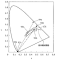
- FIG. 11 is a chromaticity diagram showing chromaticity coordinates of light emitted from the light source device according to Embodiment 2.
- FIG. 12 is a diagram for explaining functions of a vehicle using the light source device according to the second embodiment.
- FIG. 13 is a schematic cross-sectional view illustrating the configuration and functions of a light source device according to a modification of the second embodiment.
- FIG. 14 is a diagram illustrating a specific configuration of a wavelength conversion element used in a light source device according to a modification of the second embodiment.
- FIG. 15 is a schematic cross-sectional view illustrating a schematic configuration of the wavelength conversion element according to the third embodiment.
- FIG. 16 is a cross-sectional view showing a more specific configuration of the wavelength conversion element used in the light source device of the third embodiment.
- FIG. 17 is a schematic cross-sectional view showing each step of the method of manufacturing the wavelength conversion element according to the third embodiment.
- FIG. 18A is a schematic cross-sectional view showing a configuration of a wavelength conversion element according to a modification of the third embodiment.
- FIG. 15 is a schematic cross-sectional view illustrating a schematic configuration of the wavelength conversion element according to the third embodiment.
- FIG. 16 is a cross-sectional view showing a more specific configuration of the wavelength conversion element used in the light source device of the third embodiment.
- FIG. 17 is a schematic cross-sectional view showing each step of the
- FIG. 18B is a schematic cross-sectional view showing a configuration of a wavelength conversion element according to Modification 2 of Embodiment 3.
- FIG. 18C is a schematic cross-sectional view illustrating a configuration of a wavelength conversion element according to Modification 3 of Embodiment 3.
- FIG. 19 is a schematic cross-sectional view illustrating a schematic configuration of the light source device according to Embodiment 4.
- FIG. 20 is a block diagram illustrating a path of light propagated from the semiconductor light emitting device and light emitted from the wavelength conversion element, and a path of signals from each photodetector in the light source device according to the fourth embodiment. is there.
- FIG. 21 is a flowchart illustrating a signal processing flow in the light source device according to the fourth embodiment.
- FIG. 22 is a schematic cross-sectional view showing a schematic configuration of a light source device according to Modification 1 of Embodiment 4.
- FIG. 23 is a graph showing an example in which the luminance distribution and the color distribution on the light emitting surface of the emitted light in the light source device according to the first modification of the fourth embodiment and the comparative example are measured.
- FIG. 24 is a schematic cross-sectional view showing a schematic configuration of a light source device according to Modification 2 of Embodiment 4.
- FIG. 25 is a schematic cross-sectional view showing a schematic configuration of the wavelength conversion element according to the fifth embodiment.
- FIG. 26 is a schematic cross-sectional view illustrating the function of the wavelength conversion element according to the fifth embodiment.
- FIG. 27 is a schematic cross-sectional view showing a schematic configuration of a wavelength conversion element used in a light source device according to a modification of the fifth embodiment.
- FIG. 28 is a schematic cross-sectional view showing a schematic configuration of a wavelength conversion element used in the light source device according to Embodiment 6.
- FIG. 29 is a schematic cross-sectional view showing each step of the method of manufacturing the wavelength conversion element according to the sixth embodiment.
- FIG. 30 is a schematic cross-sectional view showing a schematic configuration of the wavelength conversion element used in the light source device according to the first modification of the sixth embodiment.
- FIG. 31A is a cross-sectional view schematically showing a schematic configuration of a wavelength conversion element used in a light source device according to Modification 2 of Embodiment 6.
- FIG. 31B is a cross-sectional view schematically showing a schematic configuration of the wavelength conversion element used in the light source device according to Modification 3 of Embodiment 6.
- FIG. 31C is a cross-sectional view schematically showing a schematic configuration of the wavelength conversion element used in the light source device according to Modification 4 of Embodiment 6.
- FIG. 32 is a cross-sectional view schematically showing a schematic configuration of the light source device according to Embodiment 6.
- FIG. 33 is a schematic cross-sectional view illustrating a schematic configuration of a wavelength conversion element used in the light source device according to Embodiment 7.
- FIG. 34 is a schematic perspective view showing an outline of the configuration and operation of the light source device according to the seventh embodiment.
- FIG. 35 is a schematic cross-sectional view showing a schematic configuration of a wavelength conversion element used in a light source device according to a modification of the seventh embodiment.
- FIG. 36 is a schematic cross-sectional view showing the configuration and functions of the light source device according to Embodiment 8.
- FIG. 37 is a schematic cross-sectional view showing the configuration and function of a light source device according to a modification of the eighth embodiment.
- FIG. 38 is a schematic cross-sectional view showing a specific configuration when a light projecting member is attached to a light source device according to a modification of the eighth embodiment.
- FIG. 39 is a schematic view of a conventional light source device.
- the present disclosure also includes various modifications in which the present embodiment has been modified within the scope conceived by those skilled in the art. In addition, it is possible to combine at least some of the plurality of embodiments without departing from the gist of the present disclosure.
- the term “upward” does not indicate the upward direction (vertically upward) in absolute space recognition, but is a term defined by a relative positional relationship based on the stacking order in the stacking configuration.
- the term “above” means not only when two components are spaced apart from each other and another component is present between the two components, but the two components are in close contact with each other. It is also applied to the case where two components are in contact with each other.
- Embodiment 1 The light source device according to Embodiment 1 will be described below with reference to the drawings.
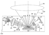
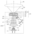
- FIG. 1 is a schematic cross-sectional view showing a schematic configuration of a light source device 100 according to the present embodiment.
- the light source device 100 includes a semiconductor light emitting device 10, a condensing optical system 20, and a wavelength conversion element 30, as shown in FIG.
- the semiconductor light emitting device 10 is a device that emits coherent excitation light, and includes a semiconductor light emitting element 11.
- the semiconductor light emitting element 11 is a semiconductor laser element (for example, a laser chip) made of a nitride semiconductor, for example, and emits laser light having a peak wavelength between 380 nm and 490 nm as excitation light 81. As shown in FIG. 1, in the present embodiment, semiconductor light emitting element 11 is mounted on a support member 12 such as a silicon carbide substrate and mounted on a package (not shown).
- a support member 12 such as a silicon carbide substrate and mounted on a package (not shown).
- the semiconductor light emitting element 11 has a configuration in which, for example, a first cladding, a light emitting layer that is an InGaN multiple quantum well layer, and a second cladding are stacked on a substrate that is a GaN substrate.
- an optical waveguide 11 a is formed in the semiconductor light emitting element 11.
- Electric power is input to the semiconductor light emitting element 11 from the outside of the light source device 100.
- Laser light having a peak wavelength of 445 nm, for example, generated in the optical waveguide 11 a of the semiconductor light emitting element 11 is emitted toward the condensing optical system 20 as excitation light 81.
- the condensing optical system 20 is an optical system that condenses the excitation light 81 emitted from the semiconductor light emitting element 11.
- the configuration of the condensing optical system 20 is not particularly limited as long as it can condense the excitation light 81.
- the condensing optical system 20 for example, one or a plurality of convex lenses can be used, and more specifically, an optical system in which an aspherical convex lens and a spherical convex lens are combined can be used.
- the condensing optical system 20 condenses the excitation light 81 having an emission angle in the horizontal direction and the vertical direction emitted from the semiconductor light emitting element 11, and propagates through the space while collimating or converging toward the wavelength conversion element 30.
- Propagation light 82 that is excitation light to be generated is generated.
- the propagating light 82 propagates along the central axis 82 i and is applied to the wavelength conversion element 30.
- the central axis 82i is set to have a predetermined angle from the normal line on the surface of the wavelength conversion element 30 (that is, the surface on which the propagation light 82 is incident), preferably 60 degrees or more and 80 degrees or less.
- the wavelength conversion element 30 is disposed apart from the semiconductor light emitting device 10, generates fluorescence by converting the wavelength of the excitation light emitted from the semiconductor light emitting device 10, and emits scattered light by scattering the excitation light. It is an element to be generated.
- the wavelength conversion element 30 is irradiated with the propagation light 82 as excitation light, wavelength-converts at least a part of the propagation light 82, and emits the wavelength-converted light.
- the wavelength conversion element 30 will be described with reference to FIGS. 2A, 2B, 2C, 2D, 2E, 2F, 2G, 2H, 2I, and 2J in conjunction with FIG.
- FIG. 2A is a schematic cross-sectional view showing a schematic configuration of the wavelength conversion element 30 according to the present embodiment.
- FIG. 2B is a schematic perspective view showing a schematic configuration of the wavelength conversion element 30 according to the present embodiment.
- FIG. 2C is a schematic cross-sectional view showing the function of the wavelength conversion element 30 according to the present embodiment.
- 2D, FIG. 2E, FIG. 2F, FIG. 2G, FIG. 2H, FIG. 2I, and FIG. 2J are schematic partially enlarged sectional views showing examples of the schematic configuration of the wavelength conversion element 30 according to the present embodiment. . 2D, FIG. 2E, FIG. 2F, FIG. 2G, FIG. 2H, FIG. 2I and FIG. 2J show enlarged sectional views corresponding to the inside of the broken line frame II shown in FIG. 2A.
- the wavelength conversion element 30 is irradiated with propagating light 82 emitted from the semiconductor light emitting element 11 and having a predetermined cross-sectional area and a predetermined light distribution.
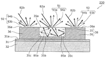
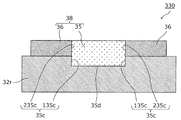
- the wavelength conversion element 30 includes a support member 32 and a wavelength conversion unit 38 disposed on the support member 32.
- the wavelength conversion unit 38 is disposed around the first wavelength conversion unit 35 and the first wavelength conversion unit 35 and surrounds the first wavelength conversion unit in a top view of the surface of the support member 32 on which the wavelength conversion unit 38 is disposed.
- a second wavelength conversion unit 36 The first wavelength conversion unit 35 and the second wavelength conversion unit 36 include a phosphor material activated with a rare earth element. The phosphor material absorbs at least part of the propagating light 82 and emits fluorescence having a wavelength different from that of the propagating light 82 as wavelength-converted light.
- the 1st wavelength conversion part 35 is the 1st surface 35a which faces the 2nd surface 35b facing the support member 32, and the 2nd surface 35b. And a side surface 35c that connects the first surface 35a and the second surface 35b.
- the wavelength conversion element 30 includes a reflecting member 31 that covers at least a part of the second surface 35b and the side surface 35c.
- the wavelength conversion element 30 includes, for example, a support member 32 having a rectangular plate shape, a reflection member 31 formed on the support member 32, and a first wavelength conversion. Unit 35 and a second wavelength conversion unit 36.
- a first wavelength conversion unit 35 is formed at the central portion of the surface 31a of the reflection member 31, and a second wavelength conversion unit 36 is formed around the first wavelength conversion unit 35.
- the surface of the first wavelength conversion unit 35 faces away from the second surface 35b facing the support member 32 (that is, located on the support member 32 side) and the second surface 35b (that is, The first surface 35a (located on the side opposite to the support member 32 side) and the side surface 35c connecting the first surface 35a and the second surface 35b.
- the side surface 35 c faces the second wavelength conversion unit 36.
- the surface of the second wavelength conversion section 36 has a second surface 36b facing the support member 32 and a first surface 36a facing away from the second surface 35b.
- the first wavelength conversion unit 35 and the second wavelength conversion unit 36 are in contact with each other at the side surface 35c.
- the average refractive index of the first wavelength conversion unit 35 is different from the average refractive index of the second wavelength conversion unit 36. That is, the average refractive index changes at the side surface 35 c that is the interface between the first wavelength conversion unit 35 and the second wavelength conversion unit 36.
- the first wavelength conversion unit 35 and the second wavelength conversion unit 36 will be described more specifically with reference to FIGS. 2D, 2E, 2F, 2G, 2H, 2I, and 2J.
- the first wavelength conversion unit 35 and the second wavelength conversion unit 36 and their interfaces in the present embodiment can be realized in a plurality of forms.
- FIG. 2D is an enlarged view of the first wavelength conversion unit 35 and the second wavelength conversion unit 36 of the wavelength conversion element 30 and their interfaces.
- the first wavelength converter 35 includes phosphor particles 155 and a transparent binder 255
- the second wavelength converter 36 includes phosphor particles 156 and a transparent binder 256.
- at least one of the phosphor particles and the transparent binder is different between the first wavelength conversion unit 35 and the second wavelength conversion unit 36.
- the average refractive index of the 1st wavelength conversion part 35 and the 2nd wavelength conversion part 36 is changed on the side surface 35c.
- the conversion efficiency to fluorescence in the second wavelength conversion unit 36 can be freely designed to have a conversion efficiency different from that of the first wavelength conversion unit 35.
- the first wavelength conversion unit 35 and the second wavelength conversion unit 36 are each composed of phosphor particles and a transparent binder, and the phosphor particles and the transparent binder constituting the first wavelength conversion unit 35 are, Fluorescence which is the same material as the phosphor particles and the transparent binder constituting the second wavelength conversion unit 36, respectively, and is the average particle diameter of the phosphor particles or the mixing ratio of the phosphor particles and the transparent binder
- a method of varying the volume ratio of the body particles here, (volume of the phosphor particles) / (volume of the phosphor particles + volume of the transparent binder) may be used. For example, as shown in FIG.
- the phosphor particles 155 and the transparent binder 255 of the first wavelength converter 35 are made of the same material as the phosphor particles 156 and the transparent binder 256 of the second wavelength converter 36, respectively. is there.
- the average particle diameter of the phosphor particles 156 of the second wavelength conversion unit 36 is smaller than that of the phosphor particles 155 of the first wavelength conversion unit 35. Thereby, the average refractive index of the 1st wavelength conversion part 35 and the 2nd wavelength conversion part 36 is changed on the side surface 35c.
- the volume ratio of the phosphor particles contained in the first wavelength converter 35 is made smaller than the volume ratio of the phosphor particles contained in the second wavelength converter 36. Thereby, the average refractive index of the 1st wavelength conversion part 35 and the 2nd wavelength conversion part 36 is changed on the side surface 35c.
- the first wavelength conversion unit 35 since the first wavelength conversion unit 35 includes the phosphor particles 155 and the transparent binder 255, excitation light (at the interface between the phosphor particles 155 and the transparent binder 255) The propagating light 82) can be scattered, and as a result, the light emission distribution can be suppressed from becoming non-uniform.
- the second wavelength conversion unit 36 since the second wavelength conversion unit 36 includes a phosphor material different from that of the first wavelength conversion unit 35, the conversion efficiency to fluorescence and the spectrum of emitted light in the second wavelength conversion unit The conversion efficiency and spectrum different from those of the one-wavelength conversion unit can be freely designed.
- the first wavelength conversion unit 35 is configured with only a single phosphor material
- the second wavelength conversion unit 36 is configured with a mixture of phosphor particles and a transparent binder.
- the first wavelength converter 35 is made of a polycrystalline phosphor material composed of a plurality of phosphor particles 155.
- the first wavelength conversion unit 35 is a conversion unit in which the refractive index of the phosphor material becomes the average refractive index. Thereby, the average refractive index of the 1st wavelength conversion part 35 and the 2nd wavelength conversion part 36 is changed on the side surface 35c.
- a plurality of pores may be included in the first wavelength conversion unit 35 formed of a single phosphor material.
- the 1st wavelength conversion part 35 can include the pore which is a scatterer while being comprised with the uniform same material which has the refractive index of fluorescent substance material.
- the first wavelength conversion unit 35 is formed of a ceramic composite including a phosphor phase and a matrix phase
- the second wavelength conversion unit 36 is formed of a mixture of phosphor particles and a transparent binder. It may be used.
- the first wavelength conversion unit 35 includes a plurality of phosphor phases 555 and a matrix phase 655.
- the average refractive index of the first wavelength conversion unit 35 and the second wavelength conversion unit 36 is changed with the side surface 35c as a boundary. Further, excitation light can be scattered at the interface 355 between the phosphor phase 555 and the matrix phase 655.
- a void 456 is provided in the matrix phase 655 or at the interface between the phosphor phase 555 and the matrix phase 655. With this configuration, the excitation light can be scattered more easily in the first wavelength conversion unit 35.
- the first wavelength conversion unit 35 and the second wavelength conversion unit 36 may include second particles 157 made of inorganic transparent particles in the transparent binder, in addition to the phosphor particles.
- the average refractive index and the light scattering property can be designed more freely in the wavelength conversion unit.
- the first wavelength conversion unit 35 and the second wavelength conversion unit 36 include the same second particles 157.
- the first wavelength conversion unit 35 and the second wavelength conversion unit 36 have different concentrations of one or both of the phosphor particles 155 and the second particles 157. That is, the ratio between the phosphor particles 155 and the second particles 157 in the wavelength conversion unit is different.
- the phosphor particles 155 and the second particles 157 may have different refractive indexes.
- the average refractive index of the first wavelength conversion unit 35 and the second wavelength conversion unit 36 can be different from each other.
- the density of the second particles 157 is high in the second wavelength conversion unit 36.
- the total amount of the interface 355 between the transparent binder and the phosphor particles and the interface 355 between the transparent binder and the second particles is made larger than that in the first wavelength conversion unit 35. Can do. As a result, the reflection of the excitation light can be enhanced at the side surface 35c.
- the first wavelength conversion unit 35 and the second wavelength conversion unit 36 include a void 158.
- the ratio of the volume of the void 158 to the volume of the wavelength conversion unit is different between the first wavelength conversion unit 35 and the second wavelength conversion unit 36.
- the structure from which the average refractive index of the 1st wavelength conversion part 35 and the 2nd wavelength conversion part 36 differs can be implement
- the total area of the interface 355 between the void 158 and the transparent binder 255, the phosphor particle 155, or the second particle 157 is different between the first wavelength conversion unit 35 and the second wavelength conversion unit 36. Therefore, the scattering degree of the excitation light inside the wavelength conversion unit can be changed.
- the amount of voids 158 is larger in the second wavelength conversion unit 36 than in the first wavelength conversion unit 35. Therefore, reflection of excitation light can be enhanced at the side surface 35c.
- the first wavelength conversion unit 35 includes a first emission region 41 where a part of the propagation light 82 is incident and emits the wavelength-converted light
- the second wavelength conversion unit 36 includes the propagation light.
- a second emission region 42 is provided in which part or all of the propagating light that is not incident on the first wavelength conversion unit 35 enters 82 and emits the wavelength-converted light.
- the first surface 35a of the first wavelength conversion unit 35 is viewed from the incident side of the propagation light 82 (in a top view of the surface of the support member 32 on which the wavelength conversion unit 38 is disposed).
- the second wavelength conversion unit 36 surrounds the periphery thereof.
- the first emission region 41 is a region corresponding to the first surface 35 a
- the second emission region 42 is a region corresponding to the first surface 36 a of the second wavelength conversion unit 36.
- the first emission region 41 coincides with the first surface 35a
- the second emission region 42 coincides with the first surface 36a.
- the first wavelength conversion unit 35 and the second wavelength conversion unit 36 generate fluorescence by wavelength-converting at least part of the incident propagation light 82, and emit the fluorescence from the first surfaces 35a and 36a, respectively. To do.
- incident light 82a which is a part of propagating light 82, enters the first emission region 41 of the first surface 35a of the first wavelength converter 35.
- a part of the incident light 82 a is wavelength-converted by the first wavelength conversion unit 35 and emitted from the first emission region 41 as fluorescence (wavelength-converted light) 94 a.
- the incident light 82 a that has not been wavelength-converted by the first wavelength conversion unit 35 is scattered and emitted from the first emission region 41 as scattered light 93 a. Therefore, the first outgoing region 41 emits outgoing light 91 that is a mixed light of the fluorescence 94a and the scattered light 93a.
- a part of the incident light 82a incident on the first wavelength conversion unit 35 is propagated through the first wavelength conversion unit 35 and becomes incident light 85a that is multiply reflected by the second surface 35b and the side surface 35c.
- the side surface 35c is configured by the interface between the first wavelength conversion unit 35 and the second wavelength conversion unit 36 having different average refractive indexes as described above, the incident light 85a can be easily reflected. .
- the fluorescence 86a generated by converting the wavelength of the incident light 85a in the first wavelength conversion unit 35 can be easily subjected to multiple reflection similarly.
- the excitation light and the fluorescence are multiple-reflected in the first wavelength conversion unit 35, so that the emission intensity distribution of the emitted light 91 in the first emission region 41 is changed between the first wavelength conversion unit 35 and the second wavelength conversion unit.
- the case where 36 has exactly the same configuration it can be made uniform.
- the second wavelength converter 36 also performs wavelength conversion.
- the incident light 82b that is a part of the propagation light 82 that is not incident on the first surface 35a is incident on the first surface 36a of the second wavelength conversion unit 36.
- a part of the incident light 82 b is wavelength-converted by the second wavelength conversion unit 36 and is emitted from the second emission region 42 as fluorescence 94 b.
- the incident light 82 b that has not been wavelength-converted by the second wavelength conversion unit 36 is scattered and emitted as scattered light 93 b from the second emission region 42. Therefore, from the second emission region 42, emission light 92 that is a mixed light of the fluorescence 94b and the scattered light 93b is emitted.
- the wavelength conversion efficiency of the second emission region 42 is designed to be lower than the wavelength conversion efficiency of the first emission region 41.
- the intensity ratio of fluorescence to scattered light is designed so that the second wavelength conversion unit 36 is lower than the first wavelength conversion unit 35.
- the conversion coefficient is a coefficient S for converting the luminous flux of the fluorescence by the visibility according to the spectrum, and the spectral distribution ⁇ e [ ⁇ ] and the visibility curve K [ ⁇ ] with respect to the wavelength ⁇ [nm]. Is calculated by the following equation 2.
- the support member 32 of the wavelength conversion element 30 is a member in which the wavelength conversion unit 38 (that is, the first wavelength conversion unit 35 and the second wavelength conversion unit 36) is disposed on the main surface.
- the support member 32 preferably has a high reflectance with respect to light having a wavelength of 380 nm to 780 nm on the main surface on which the wavelength conversion unit 38 is disposed.
- the support member 32 is preferably formed of a material having high thermal conductivity. As a result, the support member 32 increases the ratio of the amount of light emitted from the first emission region 41 to the amount of light generated by the first wavelength conversion unit 35 and dissipates the heat generated by the first wavelength conversion unit 35. Function as.
- the support member 32 is formed of, for example, a crystal material, a metal material, a ceramic material, or the like. More specifically, as the support member 32, an optical film that reflects light with a wavelength of 380 nm to 780 nm is applied to the surface of a crystal material such as silicon, sapphire, or diamond, or a ceramic material such as aluminum nitride, silicon carbide, or diamond. What was formed can be used.
- a silicon substrate is used as the support member 32, and the reflection member 31 is formed on the main surface on which the wavelength conversion unit 38 is disposed.
- a metal film such as Ag or Al can be used.
- the support member 32 may be formed with metal materials, such as silver, copper, aluminum, and those alloys.
- each of the first wavelength conversion unit 35 and the second wavelength conversion unit 36 includes a phosphor material but has an average refraction.
- the configuration is different.
- the conversion efficiency to fluorescence in the second wavelength conversion unit 36 can be freely designed to have a conversion efficiency different from that of the first wavelength conversion unit 35. Specific configurations and effects of the first wavelength conversion unit 35 and the second wavelength conversion unit 36 will be described with reference to FIGS. 2F and 2G.
- the first wavelength conversion unit 35 is, for example, Ce-activated A 3 B 5 O 12 (A includes any one of Sc, Y, Sm, Gd, Tb, and Lu. B is any one of Al, Ga, and In. And a phosphor such as a garnet crystal phosphor which is a YAG phosphor represented by More specifically, in addition to the Ce-activated Y 3 Al 5 O 12 single crystal, for example, a Ce-activated Y 3 Al 5 O 12 polycrystal as shown in FIG. 2F or a Ce as shown in FIG. 2G. A ceramic YAG phosphor in which activated Y 3 Al 5 O 12 particles and Al 2 O 3 particles are mixed and fired can be used. Said 1st wavelength conversion part 35 is fixed to the center part of the surface 31a of the reflection member 31 with adhesive agents, such as a silicone resin which is not shown in figure.
- adhesive agents such as a silicone resin which is not shown in figure.
- the second wavelength conversion unit 36 includes a YAG phosphor as in the first wavelength conversion unit 35.
- phosphor particles having an average particle diameter (median diameter) D50 of 0.5 ⁇ m to 5 ⁇ m For example, it is formed by mixing with a transparent binder such as silicone resin at a volume ratio of 50 vol%.
- the second wavelength conversion unit 36 is disposed so as to be in close contact with the side surface 35 c of the first wavelength conversion unit 35. In such a second wavelength conversion unit 36, after the first wavelength conversion unit 35 is fixed to the support member 32, the paste-like second wavelength conversion unit 36 is applied around the first wavelength conversion unit 35 and cured. Can be formed more easily.
- phosphor particles having an average particle diameter of 5 to 20 ⁇ m are used by using small particles having an average particle diameter D50 of 0.5 ⁇ m to 5 ⁇ m as the phosphor particles constituting the second wavelength conversion unit 36.
- the surface area of the fluorescent substance particle per unit volume in the 2nd wavelength conversion part 36 can be enlarged.
- the area of the interface 356 having a refractive index difference in the second wavelength conversion unit 36 can be increased. Accordingly, the ratio of scattering and reflection of incident light in the second wavelength conversion unit 36 can be increased as compared with the first wavelength conversion unit 35.
- the excitation light incident from the outside is reflected at a position closer to the surface than the first wavelength conversion unit 35 and is emitted to the outside. Therefore, since the distance of the optical path through which the excitation light propagates inside the second wavelength conversion unit 36 is shortened, the wavelength conversion efficiency of the second wavelength conversion unit 36 can be made smaller than the wavelength conversion efficiency of the first wavelength conversion unit 35. .
- the first wavelength conversion unit 35 has the same refractive index as the YAG phosphor (with a wavelength of 550 nm and a refractive index of about 1.84), and the refractive index distribution in the first wavelength conversion unit 35 is small.
- Single crystal or polycrystalline phosphor is used.
- a mixture of phosphor particles 156 that are YAG phosphors and a transparent binder 256 that is a silicone resin (refractive index: about 1.4) is used as a constituent material of the second wavelength conversion unit 36.
- the conversion unit 35 and the second wavelength conversion unit 36 are designed to have different average refractive indexes. With these configurations, as illustrated in FIG.
- the incident light 82 a incident on the first wavelength conversion unit 35 propagates through the first wavelength conversion unit 35, and is bonded to the side surface 35 c and the reflection member 31. Wavelength conversion is performed while performing multiple reflection with a certain second surface 35b.
- the fluorescence 94a converted by the first wavelength conversion unit 35 also propagates through the first wavelength conversion unit 35 and is emitted from the first emission region 41 while being subjected to multiple reflections on the second surface 35b and the side surface 35c. For this reason, even if the incident light (propagating light) 82a incident on the first emission region 41 is light having a large location dependency of the light intensity distribution, the location dependency of the light intensity distribution from the first emission region 41 is small and uniform.
- the scattered light 93a and fluorescence 94a can be emitted.
- the second wavelength conversion unit 36 has a larger scattering reflection of incident light and fluorescence near the interface than the first wavelength conversion unit 35. Therefore, the multiple reflection of incident light and fluorescence at the side surface 35c can be enhanced.
- the above effect is obtained by using a YAG phosphor as the phosphor particle 155 as the first wavelength conversion unit 35 and using Al 2 O 3 (refractive index of about 1.77) as the transparent binder 255.
- a ceramic phosphor configured as described above it is manifested. This is because the refractive index difference between the phosphor particles and the transparent binder is small as compared with the mixture of the YAG phosphor and the silicone resin (refractive index of about 1.4) constituting the second wavelength conversion unit 36.
- incident light can be easily propagated in the first wavelength conversion unit, and can be easily multi-reflected on a side surface or the like.
- FIG. 3 is a schematic cross-sectional view for explaining the function of the wavelength conversion element 30 according to the present embodiment.
- FIG. 4 is a graph showing a schematic luminance distribution in the emission region of the wavelength conversion element 30 according to the present embodiment and the wavelength conversion element according to the comparative example.
- the graph (a) in FIG. 4 shows the luminance distribution in the first emission region 41 and the second emission region 42 of the wavelength conversion element 30 according to the present embodiment.
- the graph (b) in FIG. 4 shows the luminance distribution in the emission region of the wavelength conversion element according to the comparative example.
- the wavelength conversion element 30 is irradiated with propagating light 82 from directly above or substantially oblique to the first wavelength conversion unit 35 as shown in FIG.
- the propagation light 82 for example, a laser beam having a center wavelength between 380 nm and 490 nm is irradiated from a spatially separated position.
- Laser light propagated from a spatially distant position usually has a high light intensity at the central axis 82i, and the intensity gradually decreases gradually as the distance from the central axis 82i increases. That is, the intensity distribution of the laser light propagated from a spatially separated position shows a Gaussian distribution as shown by the light intensity distribution 83 in FIG.
- the excitation light having a strong light intensity in the vicinity of the central axis 82i and the excitation light applied to the first wavelength conversion unit 35 is referred to as incident light 82a.
- excitation light that is relatively far from the central axis 82i and has a light intensity lower than that of the vicinity of the central axis 82i and that is not irradiated on the first wavelength conversion unit 35 is referred to as incident light 82b.
- the two-dimensional intensity distribution in the cross section perpendicular to the direction of the central axis 82i of the propagating light 82 is an ideal concentric Gaussian distribution.
- the light intensity of the propagation light 82 is 1 / e 2 (about 13.5%) of the maximum value from the position where the light intensity of the propagation light 82 takes the maximum value.
- the distance to the position is ⁇ 0 .
- the light intensity is 1 / e of the central intensity on the first surface 35a.
- the width of the region that is 2 or more is 2 ⁇ 0 / cos ⁇ .
- the width W3 of the first wavelength conversion unit 35 shown in FIG. 3 is set to 2 ⁇ 0 / cos ⁇ or more, the peak value of the light intensity of the incident light 82b incident on the second wavelength conversion unit 36 is changed to the first wavelength conversion. It is 13.5% or less of the peak value of the light intensity of the incident light 82a incident on the portion 35, that is, between 0 and 13.5%.
- the graph (a) in FIG. 4 schematically shows the luminance distribution of the emitted light in the first emission region 41 and the second emission region 42 when the incident light is incident on the wavelength conversion element 30 according to the present embodiment. It is shown.
- the graph (b) in FIG. 4 shows, as a comparative example, the first emission region 41 and the first emission region 41 when the incident light is incident on the wavelength conversion element in which the first wavelength conversion unit and the second wavelength conversion unit are made of the same material.
- regions is shown.
- the first emission region 41 that is the central portion of the emitted light is substantially uniform.
- the luminance distribution can be obtained, and the luminance can be suppressed low in the second emission region 42 that is the peripheral portion of the outgoing light. That is, it is possible to obtain a luminance distribution that is uniform and has high luminance only at the center of the emission region.
- the incident light 82a is multiple-reflected in the first wavelength conversion unit 35, which is the central portion of the emitted light, so that the emitted light intensity becomes uniform in the first wavelength conversion unit 35 (first emission region 41). It is to be done.
- the fluorescence 86 a generated in the first wavelength conversion unit 35 is subjected to multiple reflection and uniformization in the first wavelength conversion unit 35.
- the light beam of the emitted light from the entire wavelength conversion unit 38 is approximately the same as the light beam of the conventional wavelength conversion element.
- FIG. 5 is a diagram schematically showing a projection image obtained by the illumination device 200 in which the light projecting member 120 is combined with the light source device 100 according to the present embodiment.
- 6A and 6B are graphs showing the spectra of the emitted lights 91 and 92 in the first emission region 41 and the second emission region 42 of the light source device 100 according to the present embodiment, respectively.
- FIG. 6C is a chromaticity diagram showing the color distribution of the projection light of light source device 100 according to the present embodiment.
- FIG. 6C also shows the chromaticity coordinate area of white light defined by the ECE (Economic Commission for Europe) standard.
- the outgoing light 91 and outgoing light 92 emitted from the wavelength conversion element 30 of the present embodiment are emitted from the light source device 100 as outgoing light 95 as shown in FIG.
- the emitted light 95 becomes projection light 96 by a light projecting member 120, which is a projection lens, for example, and is projected at a predetermined position.
- the projection light 96 projected at this time is a projection image 99 a made up of projection light emitted from the first emission area 41 and a projection image made up of projection light emitted from the second emission area 42. 99b.
- the projection light forming the projection image 99b has low illuminance
- the projection light forming the projection image 99a has uniform illuminance and high.
- the illuminance changes abruptly at the boundary between the projected image 99a and the projected image 99b.
- the illumination device 200 it is possible to obtain the projection light 96 having a high contrast between the projection image 99a and the surrounding projection image 99b.
- the lighting device 200 according to the present embodiment when used for a vehicle headlamp, the illuminance on a distant road surface is increased, and the illuminance on, for example, a sidewalk around it is increased.
- the illuminance distribution can be easily controlled, for example, by reducing it.
- the chromaticity of the low illuminance region that is, the chromaticity of the projected image 99b is a mixture of the spectrum of the excitation light 81 emitted from the semiconductor light emitting device 10 and the spectrum of the fluorescence 94b generated by the second wavelength conversion unit 36.
- the resulting chromaticity is obtained. Therefore, it can suppress that the projection image 99a and the projection image 99b are comprised by the chromaticity which differs greatly. Specifically, for example, as shown in FIG. 5, when a human crosses the optical path of the projection light 96, he / she feels blue light corresponding to excitation light, and emits white light corresponding to mixed light of scattered light and fluorescence. It can suppress feeling.
- Outgoing light 91 is emitted as white light having chromaticity coordinates (0.34, 0.35) mixed with fluorescent light 94a of 0.54).
- the emitted light 91 is projected as a projected image 99a at a predetermined position.
- Outgoing light 92 which is white light having a chromaticity coordinate (0.29, 0.25) mixed with the fluorescent light 94b, is emitted.
- the emitted light 92 is projected as a projection image 99b at a predetermined position.
- the projection image 99b can project light having chromaticity coordinates closer to the projection image 99a than the scattered light 93b. For this reason, it is possible to suppress the chromaticity distribution in which the blue irradiation light exists in the peripheral region of the projection image.
- the difference in the chromaticity coordinates between the outgoing light 91 and the outgoing light 92 is due to the difference in the intensity ratio between the scattered light and the fluorescence, as shown in FIGS. 6A and 6B.
- the chromaticity coordinates of the emitted light 91 that occupies most of the emitted light 95 of the light source device 100 are included in the chromaticity coordinate region of the white light of the ECE standard.
- it can be used as a vehicle headlamp. That is, by setting the chromaticity coordinates of the white light of the entire emitted light 95 within the ECE standard, it can be used as an automotive headlamp.
- the structure of the 1st wavelength conversion part 35 and the 2nd wavelength conversion part 36 is not restricted to said structure.
- a mixed material of phosphor particles having an average particle diameter D50 ⁇ m of 5 to 20 ⁇ m and a transparent binder is used, and as the second wavelength conversion unit 36, A mixed material of phosphor particles having an average particle diameter D50 of 0.5 ⁇ m to 5 ⁇ m and a transparent binder may be used.
- the surface area of the phosphor particles per unit volume, that is, the refractive index interface 356 in the second wavelength conversion unit 36 is changed to the surface area of the phosphor particles per unit volume in the first wavelength conversion unit 35, that is, the interface of the refractive index. It can be larger than 355.
- the reflectance at the side surface 35c of the light traveling from the first wavelength conversion unit 35 to the second wavelength conversion unit 36 can be increased, and multiple reflection can be enhanced.
- the same material for example, a silicone resin, may be used as the transparent binder of the first wavelength conversion unit 35 and the second wavelength conversion unit 36.
- first wavelength conversion unit 35 when a single crystal phosphor is used as the first wavelength conversion unit 35, a plurality of first wavelength conversion units 35 are provided in the first wavelength conversion unit 35, as shown in FIG.
- An interface 355 that is a crystal grain boundary may be provided.
- pores 455a and intragranular pores 455b may be included. Thereby, it is possible to prevent the emission distribution from becoming non-uniform due to the multiple reflection of the excitation light in the first wavelength conversion unit 35 due to the increase in scattering properties.
- the phosphor constituting the first wavelength converter 35 is a phosphor particle 155 that is a YAG phosphor
- the phosphor constituting the second wavelength converter 36 is a silicate phosphor.
- the phosphor particles 156 the phosphor material in each of the first wavelength conversion unit 35 and the second wavelength conversion unit 36 may be different. Thereby, the scattering degree inside the 1st wavelength conversion part 35 and the 2nd wavelength conversion part 36 can be varied. Thereby, the wavelength conversion efficiencies of the first wavelength conversion unit 35 and the second wavelength conversion unit 36 can be freely changed.
- the chromaticity coordinates x of the first wavelength conversion unit 35 are changed to the chromaticity of the second wavelength conversion unit 36 by changing the configuration of the first wavelength conversion unit 35 and the second wavelength conversion unit 36 by the method as described above. While making it smaller than the coordinate x, the chromaticity coordinate of the white light of the whole emitted light 95 may be used as an automotive headlamp by making it within the ECE standard. In this case, it is easy to make the chromaticity coordinates of the central portion of the projected image smaller than that of the peripheral portion.
- the cross-sectional shape and cross-sectional area of the excitation light on the incident surface on which the excitation light (propagation light 82) of the first wavelength conversion unit 35 is incident may be substantially equal to the shape and area of the incident surface of the first wavelength conversion unit 35. Good. Thereby, the uniformity of the luminance distribution in the central portion of the light emitting region can be improved, and excitation light can be prevented from being emitted from the periphery of the light emitting region without being mixed with fluorescence.
- the first wavelength conversion unit 35 includes a first emission region 41 on which excitation light (propagation light 82) is incident, and a sectional shape and a sectional area of the excitation light on the incident surface on which the excitation light of the first emission region 41 is incident. May be substantially equal to the shape and area of the entrance surface in the first exit region 41.
- FIG. 7 is a schematic cross-sectional view showing a schematic configuration of an illumination device 200 using the light source device 100 according to the present embodiment.
- FIG. 8 is a schematic cross-sectional view showing a specific configuration of the wavelength conversion element 30 in the light source device 100 according to the present embodiment.
- the semiconductor light emitting device 10 the condensing optical system 20, and the wavelength conversion element 30 are fixed to a housing 50 made of, for example, an aluminum alloy. And the housing
- the semiconductor light emitting device 10 is mounted on a package 13 in which the semiconductor light emitting element 11 is, for example, a TO-CAN package.
- the first wavelength conversion unit 35 is fixed to the reflection member 31 on the support member 32, and the second wavelength conversion unit 36 is formed around the first wavelength conversion unit 35.
- the light source device 100 configured in this way is fixed to a heat radiating member 75 that is a heat radiating fin, for example.
- a light projecting member 120 that is, for example, a projection lens is disposed on the optical path of the emitted light 91 and 92 of the light source device 100.
- the lighting device 200 including the light source device 100, the light projecting member 120, and the heat radiating member 75 can be configured.
- the first wavelength conversion unit 35 and the second wavelength conversion unit 36 are, for example, a reflective member 31 formed of a metal oxide film such as SiO 2 or TiO 2 or a metal film such as Ag or Al. Formed on the surface 31a.
- the reflection member 31 is supported by a support member 32 made of, for example, a silicon substrate. Further, for example, an unevenness 32c as shown in FIG. 8 is formed on the surface of the support member 32 made of, for example, a silicon substrate by using lithography and etching, and reflection is performed on the surface of the support member 32 on which the unevenness 32c is formed.
- the member 31 may be formed.
- the first wavelength conversion portion 35 that is a ceramic phosphor obtained by mixing and sintering Ce-activated YAG phosphor and Al 2 O 3 is used, for example, by using a bonding material 34 that is a silicone-based adhesive. Fix it. At this time, it is preferable to form uneven surfaces on the first surface 35a, the second surface 35b, and the side surface 35c of the first wavelength conversion unit 35 to enhance multiple reflection and scattering of light.
- a second wavelength conversion unit 36 comprising:
- the wavelength conversion element 30 can be easily configured.
- an adhesive layer 39 made of a metal film such as Ti or Au is formed on the surface of the support member 32 where the wavelength conversion section 38 is not disposed, and is fixed to the housing 50 with solder (not shown) or the like.
- FIG. 9A is a schematic cross-sectional view showing a schematic configuration of a wavelength conversion element 30A according to Modification 1 of the present embodiment.
- FIG. 9B is a schematic cross-sectional view showing a schematic configuration of a wavelength conversion element 30B according to Modification 2 of the present embodiment.
- FIG. 10A is a schematic cross-sectional view showing a schematic configuration of a wavelength conversion element 30C according to Modification 3 of the present embodiment.
- FIG. 10B is a schematic cross-sectional view showing a schematic configuration of a wavelength conversion element 30D according to Modification 4 of the present embodiment.
- the second wavelength conversion unit 36 covers the peripheral portion of the first surface 35a (the upper surface in FIG. 9A) of the first wavelength conversion unit 35, as in the wavelength conversion element 30A according to the first modification illustrated in FIG. 9A. Good. In other words, portions other than the central portion of the first surface 35 a of the first wavelength conversion unit 35 may be covered with the second wavelength conversion unit 36.
- the first emission region 41 is a central region of the first surface 35a that is not covered by the second wavelength conversion unit 36, that is, the first surface 35a. Of these, it can be defined as an area exposed to the outside.
- the incident light 85a multiple-reflected by the first wavelength conversion unit 35 reflects not only the side surface 35c and the second surface 35b but also a part of the first surface 35a.
- the wavelength conversion efficiency in the 1 wavelength conversion part 35 can be made high.
- the thickness of the second wavelength conversion unit 36 on the first wavelength conversion unit 35 is made thinner than the thickness of the first wavelength conversion unit 35. Preferably, it is less than half.
- the emitted light 91 emitted from the first wavelength conversion unit 35 can be emitted through the second wavelength conversion unit 36 on the first wavelength conversion unit 35, so that the first embodiment Similarly to the above, it is possible to improve the uniformity of the luminance distribution in the central portion of the light emitting region of the wavelength conversion element.
- the wavelength conversion element 30A includes a support member 32r formed of a material having a high reflectance with respect to light having a wavelength of 380 nm to 780 nm.
- the support member 32r is formed of a metal material such as silver, copper, aluminum, and alloys thereof. Thereby, it is not necessary to provide a separate reflecting member on the support member.
- the support member 32r having high heat dissipation performance can be realized by forming the support member 32r with a metal material having high thermal conductivity.
- the thickness of the second wavelength conversion unit 36 can be made thinner than the thickness of the first wavelength conversion unit 35. For this reason, the wavelength conversion efficiency of a 2nd wavelength conversion part can be made low easily with respect to a 1st wavelength conversion part. Therefore, the contrast of the luminance distribution between the central portion and the peripheral portion of the light emitting region of the wavelength conversion element can be increased.
- the first wavelength conversion unit 35 is fixed on the support member 32, and the second wavelength conversion unit 36 surrounds the first wavelength conversion unit 35. It is formed. At this time, between the first wavelength converter 35 and the support member 32, for example, it may be provided with a reflecting member 31 TiO 2 particles are dispersed in 10 ⁇ m average particle diameter of 0.1 to the silicone resin.
- the reflection member 31 may be formed only between the first wavelength conversion unit 35 and the support member 32.
- the light that has reached the second surface 35 b of the first wavelength conversion unit 35 among the light that has entered the first wavelength conversion unit 35 is reflected by the reflecting member 31.
- the incident light 82 a is efficiently converted into the fluorescence 94 a in the first wavelength conversion unit 35, and the emitted light 91 with high luminance can be emitted from the first wavelength conversion unit 35.
- the reflection member 31 is not provided between the second wavelength conversion unit 36 and the support member 32.
- the contrast can be increased.
- the side surface 35c of the first wavelength conversion unit 35 may be inclined. That is, it does not have to be orthogonal to the surface of the support member 32r on which the first wavelength conversion unit 35 is disposed.
- the structure of fluorescent substance material and a transparent binder is not limited to said structure.
- the phosphor material examples include oxynitride phosphors (for example, ⁇ -SiAlON: Eu 2+ , Ca- ⁇ -SiAlON: Eu 2+ , (Ca, Sr, Ba) SiO 2 N 2 : Eu 2+ ), nitriding, and the like.
- oxynitride phosphors for example, ⁇ -SiAlON: Eu 2+ , Ca- ⁇ -SiAlON: Eu 2+ , (Ca, Sr, Ba) SiO 2 N 2 : Eu 2+ ), nitriding, and the like.
- Phosphor for example, CaAlSiN 3 : Eu 2+ or (La, Y, Gd) 3 Si 6 N 11 : Ce 3+
- silicate-based phosphor for example, Sr 3 MgSi 2 O 8 : Eu 2+ , (Ba, Sr, Mg) 2 SiO 4 : Eu 2+
- phosphate-based phosphors Sr 5 (PO 4 ) 3 Cl: Eu 2+ etc.
- quantum dot phosphors nanoparticles such as InP, CdSe
- the first wavelength conversion unit 35 is configured by combining a plurality of phosphors, the chromaticity coordinates of the fluorescence emitted from the first wavelength conversion unit 35, and the excitation light reflected by the first wavelength conversion unit 35 White light can also be emitted from the light source device 100 by combining the chromaticity coordinates.
- the semiconductor light emitting device 11 that emits near-ultraviolet excitation light having a peak wavelength of about 405 nm, as a phosphor material, Sr 5 (PO 4 ) 3 Cl: Eu 2+ that is a blue phosphor
- White light is obtained by using a combination with YAG: Ce 3+ which is a yellow phosphor.
- YAG: Ce 3+ or (La, Y) 3 Si 6 N 11 Ce 3+ that is a yellow phosphor as a phosphor material.
- White light can be obtained by using.
- a transparent binder for holding the phosphor material when a material containing a siloxane bond is used, for example, a binder containing a high heat resistant silicone resin or silsesquioxane can be used.
- materials such as SiO 2 , ZnO, ZrO 2 , Nb 2 O 5 , Al 2 O 3 , TiO 2 , SiN, and AlN can be used.
- Embodiment 2 Next, the light source device according to Embodiment 2 will be described.
- the structure of the light source device according to the present embodiment is the same as the structure of the light source device according to the first embodiment shown in FIGS. 1 to 5 and FIGS. .
- the second wavelength conversion unit 36 includes a phosphor material different from that of the first wavelength conversion unit 35. Therefore, the conversion efficiency to the fluorescence in the 2nd wavelength conversion part and the spectrum of emitted light can be freely designed to the conversion efficiency and spectrum different from a 1st wavelength conversion part.
- the x coordinate of the chromaticity coordinate of the fluorescence generated by the second wavelength conversion unit 36 is compared with the x coordinate of the chromaticity coordinate of the fluorescence generated by the first wavelength conversion unit 35. It is large.
- the light source device according to the present embodiment will be described with reference to the drawings.
- FIG. 11 is a chromaticity diagram showing chromaticity coordinates of light emitted from the light source device according to the present embodiment.
- scattered light 93a and fluorescence 94a emitted from the first wavelength conversion unit 35 of the light source device according to the present embodiment, scattered light 93b emitted from the second wavelength conversion unit 36, and The chromaticity coordinates of the fluorescence 94b and the projection images 99a and 99b which are mixed light are plotted.
- the x coordinate of the chromaticity coordinate of the fluorescence 94b generated by the second wavelength conversion unit 36 is larger than the x coordinate of the chromaticity coordinate of the fluorescence 94a generated by the first wavelength conversion unit 35.
- the chromaticity coordinates of the projection image 99a emitted from the first wavelength conversion unit 35 and the projection image 99b emitted from the second wavelength conversion unit 36 are substantially on the black body radiation locus.
- the amount of scattered light 93b in the second wavelength conversion unit 36 is much smaller than the amount of scattered light 93a in the first wavelength conversion unit 35 due to absorption. Further, the light amount of the wavelength converted light (fluorescence 94b) in the second wavelength conversion unit 36 is lower than the light amount of the wavelength converted light (fluorescence 94a) in the first wavelength conversion unit 35. That is, in the outgoing light emitted from the second wavelength converter 36, the ratio of the scattered light 93b to the fluorescence 94b is lower than the ratio of the scattered light 93a to the fluorescent light 94a in the outgoing light emitted from the first wavelength converter 35. At this time, the color temperature of the projected image 99b is lower than the color temperature of the projected image 99a. For this reason, the visibility of the projected image 99b is lower than that of the projected image 99a. Therefore, the contrast between the projection image 99a having a high light intensity and the projection image 99b having a low light intensity can be further increased.
- the chromaticity coordinates of the projected image 99a and the projected image 99b are both plotted on the black body radiation locus. For this reason, the light which forms the projection image 99a and the projection image 99b does not become unnatural white light. For example, when the ratio of blue scattered light is large in the projected image 99b, the pale projected image 99b is projected around the white projected image 99a, and it is felt as unnatural projected light for the users. However, in the light source device according to the present embodiment, white light with low light intensity and low visibility is projected around the white projection image 99a, so that the user can be prevented from feeling unnatural.
- the light source device is, for example, for a vehicle It can be used as a headlight.
- FIG. 12 is a diagram for explaining functions of the vehicle using the light source device according to the present embodiment.
- the propagating light 82 is incident from the support member side of the wavelength conversion element.
- the support member of the wavelength conversion element is made of a material that is transparent to the propagation light 82.
- FIG. 13 is a schematic cross-sectional view showing the configuration and function of the light source device 101 according to this modification.
- FIG. 14 is a diagram illustrating a specific configuration of the wavelength conversion element 130 used in the light source device 101 according to the present modification.
- the light source device 101 includes a semiconductor light emitting device 10, a condensing optical system 20, and a wavelength conversion element 130.
- the semiconductor light emitting device 10 is the same device as the semiconductor light emitting device 10 according to the first embodiment.
- the semiconductor light emitting device 10 is a device in which a semiconductor light emitting element 11, for example, a nitride semiconductor laser is mounted on a support member 12 and fixed to a package (not shown).
- Excitation light 81 emitted from the optical waveguide 11 a formed in the semiconductor light emitting element 11 is emitted toward the condensing optical system 20.
- the condensing optical system 20 condenses the excitation light 81 having an emission angle in the horizontal direction and the vertical direction emitted from the semiconductor light emitting element 11, and propagates through the space while collimating or converging toward the wavelength conversion element 130.
- Propagation light 82 that is excitation light to be generated is generated.
- the propagating light 82 propagates along the central axis 82 i and is irradiated on the wavelength conversion element 130.
- the condensing optical system 20 is, for example, a lens.
- the wavelength conversion element 130 is disposed apart from the semiconductor light emitting device 10, generates fluorescence by converting the wavelength of excitation light emitted from the semiconductor light emitting device 10, and transmits transmitted light by transmitting the excitation light. It is an element to be generated.
- the wavelength conversion element 130 includes a support member 32 and a wavelength conversion unit 38 disposed on the support member 32, and the wavelength conversion unit 38 is disposed around the first wavelength conversion unit 35 and the first wavelength conversion unit 35. And a second wavelength conversion unit 36 surrounding the first wavelength conversion unit 35 in a top view of the surface of the support member 32 on which the wavelength conversion unit 38 is disposed.
- the intensity ratio of fluorescence to transmitted light is lower in the second wavelength conversion unit 36 than in the first wavelength conversion unit 35.
- the reflection member 31 that is an optical film that reflects fluorescence is formed on one main surface of the support member 32 that is a substrate transparent to the propagation light 82. . And the 1st wavelength conversion part 35 and the 2nd wavelength conversion part 36 are fixed to the surface 31a of the reflection member 31.
- FIG. 1st wavelength conversion part 35 and the 2nd wavelength conversion part 36 are fixed to the surface 31a of the reflection member 31.
- the support member 32 for example, a sapphire substrate having a thickness of 0.33 mm and optically polished on both sides is used. Then, a reflective member 31 that is a dichroic film, for example, is formed on one main surface of the support member 32 (the upper surface in FIG. 14).
- the reflecting member 31 is formed of a dielectric multilayer film, and transmits light having a wavelength shorter than 490 nm and reflects light having a wavelength of 490 nm or more in a direction perpendicular to the surface. It is designed to reflect light having a wavelength shorter than 490 nm as the incident angle with respect to the surface increases.
- An antireflection film 33 made of one or more dielectric films is formed on the other main surface of the support member 32 (the lower surface in FIG. 14).
- the first wavelength conversion unit 35 and the second wavelength conversion unit 36 are fixed to the surface 31a of the support member 32 on the reflection member 31 side.
- the first wavelength conversion unit 35 is phosphor particles 155 made of, for example, a Ce-activated YAG phosphor.
- the average particle diameter D50 of the phosphor particles 155 is between 1 ⁇ m and 20 ⁇ m.
- the phosphor particles 155 are fixed on the reflecting member 31 with a transparent binder 255 made of, for example, silsesquioxane.
- the first wavelength conversion unit 35 has a diameter of 600 ⁇ m and a thickness of 70 ⁇ m, for example, on the surface of the reflection member 31.
- the first wavelength conversion unit 35 is formed on the reflection member 31 by an opening mask (not shown).
- the opening mask has a thickness of 70 ⁇ m and an opening having a diameter of 600 ⁇ m at the center. Using such an opening mask, a paste-like member in which phosphor particles 155 are mixed with a solution-like transparent binder 255 is transferred onto the reflecting member 31 and cured to easily form the first wavelength converter 35. it can.
- the second wavelength conversion unit 36 is formed by applying a mixed material of phosphor particles different from the first wavelength conversion unit 35 and a transparent binder around the first wavelength conversion unit 35 and curing it.
- the propagating light 82 is incident from the antireflection film 33 side of the wavelength conversion element 130 having the above-described configuration.
- the incident light incident on the first wavelength conversion unit 35 becomes incident light 85 a scattered at the interface between the phosphor particles 155 and the transparent binder 255, and further, the first wavelength conversion unit 35 and the first wavelength conversion unit 35.
- Multiple reflection is performed on the side surface 35 c that is the interface of the two-wavelength conversion unit 36 and the second surface 35 b that is the interface between the first wavelength conversion unit 35 and the reflecting member 31.
- a part of the multiple reflected incident light 85a is wavelength-converted by the phosphor particles 155 to become fluorescence 86a.
- the fluorescence 86a is multiple-reflected inside the first wavelength conversion unit 35 in the same manner as the incident light 85a.
- the incident light 85a and the fluorescence 86a are uniformly distributed in the first wavelength conversion unit 35, and are emitted from the first surface 35a of the first wavelength conversion unit 35 as scattered light 93a and fluorescence 94a that are transmitted light. .
- a part of the propagation light 82 incident on the second wavelength conversion unit 36 is wavelength-converted in the second wavelength conversion unit 36 and emitted from the first surface 36a of the second wavelength conversion unit 36 as fluorescence 94b.
- another part of the propagation light 82 incident on the second wavelength conversion unit 36 is multiple-reflected in the second wavelength conversion unit 36 and emitted as scattered light 93b which is transmitted light.
- the outgoing light 91 which is a mixed light of the scattered light 93a (transmitted light) and the fluorescent light 94a
- the outgoing light which is a mixed light of the scattered light 93b (transmitted light) and the fluorescent light 94b
- Irradiation light 92 is emitted.
- the emitted light 95 composed of the emitted light 91 and the emitted light 92 is emitted from the light source device 101 and becomes projection light 96 that is substantially parallel light by a light projecting member 120 that is provided outside the light source device 101, for example, a projection lens. Is emitted.
- the scattered light 93a and fluorescence 94a emitted from the first wavelength conversion unit 35, the scattered light 93b and fluorescence 94b emitted from the second wavelength conversion unit 36, and the chromaticity coordinates of the projection images 99a and 99b are as follows: For example, the coordinates are plotted in the chromaticity diagram of FIG. In this modification, the chromaticity coordinates of the projection image 99a emitted from the first wavelength conversion unit 35 and the projection image 99b emitted from the second wavelength conversion unit 36 are almost on the black body radiation locus. .
- the color temperature of the projected image 99b is lower than that of the projected image 99a. For this reason, the visibility of the projected image 99b is lower than that of the projected image 99a. Accordingly, it is possible to increase the contrast between the projection image 99a having a high light intensity and the projection image 99b having a low light intensity.
- the chromaticity coordinates of the projected image 99a and the projected image 99b are both on the black body radiation locus, they do not become unnatural white light.
- the first wavelength conversion unit 35 of the light source device 102 includes a first emission region 41 where the propagation light 82 (excitation light) is incident and the transmission light is emitted, and the propagation of the first emission region 41 is performed.
- the cross-sectional shape and cross-sectional area of the propagation light 82 on the incident surface on which the light 82 is incident may be substantially equal to the shape and area of the incident surface in the first emission region 41.
- the light source device of the present embodiment can also be used as a vehicle headlamp, for example, as in the above embodiments.
- the light source device according to the present embodiment will be described.
- the wavelength conversion element used in the light source device according to the present embodiment not only the side surface 35c of the first wavelength conversion unit 35 but also the second surface 35b on the support member 32 side is covered with the second wavelength conversion unit 36. It is different from the light source device 100 according to the first embodiment.
- the light source device according to the present modification will be described with reference to the drawings with a focus on differences from the wavelength conversion element 30 of the light source device according to the first embodiment.
- FIG. 15 is a schematic cross-sectional view showing a schematic configuration of the wavelength conversion element 230 according to the present embodiment.
- the wavelength conversion element 230 includes a support member 32, a reflection member 31, and a wavelength conversion unit 38.
- the support member 32 is, for example, a silicon substrate.
- the reflection member 31 is a reflection film made of a metal film such as titanium, platinum, aluminum, or silver, and is formed on the surface of the support member 32 on which the wavelength conversion unit 38 is disposed. Note that an aluminum plate or an aluminum alloy plate may be used as the support member 32. In this case, since the support member 32 has a function of a reflection member, the reflection member 31 may not be provided separately.
- the wavelength conversion unit 38 includes a first wavelength conversion unit 35 and a second wavelength conversion unit 36.
- the first wavelength conversion unit 35 is a ceramic member including, for example, a YAG phosphor, and is disposed on the reflection member 31. As shown in FIG. 15, of the surface of the first wavelength conversion unit 35, other than the first surface 35 a (upper surface in FIG. 15) on which the incident light 82 a is incident, that is, the first surface on the side surface 35 c and the support member 32 side. The two surfaces 35 b are covered with the second wavelength conversion unit 36.
- the second wavelength conversion unit 36 for example, a mixed material of phosphor particles that are YAG phosphor particles and a transparent binder 256 that is silsesquioxane can be used.
- the average refractive index can be made different between the first wavelength conversion unit 35 and the second wavelength conversion unit 36. Therefore, a part of the incident light 82a incident on the first wavelength conversion unit 35 is converted into a side surface 35c that is an interface between the first wavelength conversion unit 35 and the second wavelength conversion unit 36 disposed in the outer peripheral region thereof, Multiple reflection can be performed by the first wavelength conversion unit 35 and the second surface 35b which is an interface between the first wavelength conversion unit 35 and the second wavelength conversion unit 36 disposed between the support member 32. Thereby, the emitted light 91 with a uniform light distribution can be efficiently emitted from the first wavelength conversion unit 35.
- FIG. 16 is a cross-sectional view showing a more specific configuration of the wavelength conversion element 230 used in the light source device of the present embodiment.
- the support member 32 is a silicon substrate. Concavities and convexities are formed on the surface of the support member 32 on which the first wavelength conversion unit 35 is disposed by using wet etching or dry etching.
- a reflective member 31 that is a reflective film made of a metal film such as titanium, platinum, aluminum, silver, or the like is formed on the surface on which the unevenness is formed.
- the 1st wavelength conversion part 35 which is a ceramic member containing a YAG type fluorescent substance is arrange
- the first wavelength conversion unit 35 is a ceramic YAG phosphor in which Ce-activated Y 3 Al 5 O 12 particles and Al 2 O 3 particles are mixed and fired, and has a thickness of, for example, 400 ⁇ m square to 500 ⁇ m square and a thickness of 50 ⁇ m to 100 ⁇ m. It is a size.
- the surface of the first wavelength conversion unit 35 is formed with unevenness by physical processing such as grinding or chemical processing such as wet etching or dry etching.
- the second wavelength conversion unit 36 for example, phosphor particles 156, which are YAG phosphor particles having a particle diameter distributed from 1 ⁇ m to 4 ⁇ m, are fixed with a transparent binder 256, for example, silsesquioxane. Is used.
- the particle size being distributed from 1 ⁇ m to 4 ⁇ m means that the average particle size D50 is 2 ⁇ m, D10 is 1 ⁇ m, and D90 is 4 ⁇ m.
- the refractive indexes of Ce-activated Y 3 Al 5 O 12 particles and Al 2 O 3 particles constituting the first wavelength conversion unit 35 are approximately 1.84 and 1.77, respectively.
- the refractive indexes of Ce-activated Y 3 Al 5 O 12 particles and silsesquioxane constituting the second wavelength conversion unit 36 are approximately 1.84 and 1.5, respectively. Therefore, the second wavelength conversion unit 36 has a larger refractive index difference between the phosphor particles and the transparent binder than the first wavelength conversion unit 35, and is reflected at a position where the distance from the surface is small.
- the first wavelength converter The outgoing light 91 having a uniform light distribution can be efficiently emitted from the portion 35.
- a part of the incident light 82 b incident on the second emission region 42 in the propagating light 82 is wavelength-converted by the phosphor particles 156 of the second wavelength conversion unit 36 and emitted from the wavelength conversion element 30 as fluorescence 94 b. .
- the contrast of the emitted light can be increased at the boundary between the first emission region 41 and the second emission region 42.
- the incident light 82b incident on the second emission region 42 becomes fluorescence 94b, it is mixed with the scattered light 93b emitted from the second emission region 42 and emitted from the wavelength conversion element. For this reason, the chromaticity coordinates of the outgoing light 92 emitted from the second outgoing area 42 are different from those in the case where only the scattered light of the incident light 82b is emitted from the second outgoing area 42. 41 is close to the chromaticity coordinates of the outgoing light 91 emitted from 41.
- the color distribution of the light emitted from the light source device can be further reduced.
- FIG. 17 is a schematic cross-sectional view showing each step of the method of manufacturing the wavelength conversion element 230 according to the present embodiment.
- an average particle diameter D50 is 1 ⁇ m to 4 ⁇ m on a reflective member 31 formed of a metal film, for example, formed on a support member 32 made of a silicon substrate.
- a paste-like second wavelength conversion unit 36 in which phosphor particles distributed between the two are mixed with a transparent binder is applied.
- the transparent binder a paste-like transparent binder in which silsesquioxane is dissolved in an organic solvent is used.
- the first wavelength conversion unit 35 is held by the vacuum collet 150.
- the first wavelength conversion unit 35 is disposed on the paste-like second wavelength conversion unit 36.
- the paste-like second wavelength conversion unit 36 rises due to the intermolecular force between the first wavelength conversion unit 35 and the transparent binder. For this reason, the lower surface of the 1st wavelength conversion part 35 and at least one part of a side surface can be easily covered with the paste-like 2nd wavelength conversion part 36.
- the second wavelength conversion unit 36 is cured by heating.
- the organic solvent of the paste-like second wavelength conversion unit 36 is volatilized and cured.
- the wavelength conversion element of the light source device of the present embodiment can be easily manufactured.
- the paste-like second wavelength conversion part 36 contracts, irregularities along the phosphor particles can be easily formed on the surface of the second wavelength conversion part 36. Thereby, the propagation light 82 can be scattered on the surface of the second wavelength conversion unit 36.
- the wavelength conversion element 230 of the light source device according to the present embodiment can be easily manufactured by the above manufacturing method.
- FIG. 18A is a schematic cross-sectional view showing a configuration of a wavelength conversion element 230A according to Modification 1 of the present embodiment.
- FIG. 18B is a schematic cross-sectional view showing a configuration of a wavelength conversion element 230B according to Modification 2 of the present embodiment.
- FIG. 18C is a schematic cross-sectional view showing a configuration of a wavelength conversion element 230C according to Modification 3 of the present embodiment.
- the second wavelength conversion unit 36 may cover the peripheral portion of the first surface 35a (the upper surface in FIG. 18A) of the first wavelength conversion unit 35. Good. In other words, the second wavelength conversion unit 36 may cover a portion other than the central portion of the first surface 35 a of the first wavelength conversion unit 35.
- the wavelength conversion element 230A having such a configuration can be easily configured by increasing the coating amount of the second wavelength conversion unit 36 shown in the cross-sectional view (a) in the manufacturing method shown in FIG.
- the incident light 85a multiple-reflected by the first wavelength conversion unit 35 reflects not only the side surface 35c and the second surface 35b but also a part of the first surface 35a.
- the wavelength conversion efficiency in the 1 wavelength conversion part 35 can be made high.
- the thickness of the second wavelength conversion unit 36 on the first wavelength conversion unit 35 is made thinner than the thickness of the first wavelength conversion unit 35. Preferably, it is less than half.
- the emitted light 91 emitted from the first wavelength conversion unit 35 can be emitted through the second wavelength conversion unit 36 on the first wavelength conversion unit 35, so that the wavelength conversion element 230 ⁇ / b> A It is possible to improve the uniformity of the luminance distribution in the central portion of the light emitting region.
- the wavelength conversion element 230A having such a configuration can be easily formed by reducing the coating amount of the second wavelength conversion section 36 shown in the cross-sectional view (a) in the manufacturing method shown in FIG.
- the thickness of the second wavelength conversion unit 36 can be made thinner than the thickness of the first wavelength conversion unit 35. For this reason, the wavelength conversion efficiency of a 2nd wavelength conversion part can be easily made low with respect to a 1st wavelength conversion part. Therefore, in the light emission distribution of the light emitting region of the wavelength conversion element, the contrast between the first emission region and the second emission region can be increased.
- the second wavelength conversion unit 36 covers only the second surface 35b of the first wavelength conversion unit 35.
- the wavelength conversion element 230A having such a configuration can be easily configured by reducing the application amount of the second wavelength conversion unit 36 shown in the cross-sectional view (a) in the manufacturing method shown in FIG.
- the thickness of the second wavelength conversion unit 36 can be made thinner than the thickness of the first wavelength conversion unit 35. For this reason, the wavelength conversion efficiency of a 2nd wavelength conversion part can be easily made low with respect to a 1st wavelength conversion part.
- the light source device according to the present embodiment is different from the light source devices according to the above embodiments in that the light source device mainly includes a photodetector.
- the light source device according to the present embodiment will be described with reference to the drawings.
- FIG. 19 is a schematic cross-sectional view showing a schematic configuration of the light source device 102 according to the present embodiment.
- the light source device 102 shown in FIG. 19 includes a semiconductor light emitting device 10, a wavelength conversion element 30, a first filter 23, a first photodetector 25, a second photodetector 26, and a third photodetector 27. Is provided.
- the light source device 102 further includes a condensing optical system 20, a separation optical element 21, and a second filter 24.
- the semiconductor light emitting device 10 is a device that emits laser light.
- the semiconductor light emitting device 10 is a device that emits coherent excitation light 81 and includes the semiconductor light emitting element 11.
- the semiconductor light emitting device 10 is fixed so that the emitted light emitted from the semiconductor light emitting element 11 is emitted toward the wavelength conversion element 30.
- the semiconductor light emitting element 11 is a semiconductor laser element made of, for example, a nitride semiconductor, and emits laser light having a peak wavelength between wavelengths 380 nm and 490 nm as excitation light 81.
- the semiconductor light emitting element 11 is mounted on a package 13 which is, for example, a TO-CAN package.
- an optical waveguide 11 a is formed in the semiconductor light emitting element 11.
- Electric power is input to the semiconductor light emitting element 11 from the outside of the light source device 100.
- Laser light having a peak wavelength of 445 nm, for example, generated in the optical waveguide 11 a of the semiconductor light emitting element 11 is emitted toward the condensing optical system 20 as excitation light 81.
- the condensing optical system 20 is an optical system that condenses the excitation light 81 that is laser light emitted from the semiconductor light emitting element 11 and irradiates the wavelength conversion element 30.
- the configuration of the condensing optical system 20 is not particularly limited as long as it can condense the excitation light 81.
- the condensing optical system 20 condenses the excitation light 81 having an emission angle in the horizontal direction and the vertical direction emitted from the semiconductor light emitting element 11, and propagates through the space while collimating or converging toward the wavelength conversion element 30.
- Propagation light 82 that is excitation light to be generated is generated.
- the propagating light 82 is applied to the wavelength conversion element 30.
- the wavelength conversion element 30 is an element that emits fluorescence when the laser light emitted from the semiconductor light emitting device 10 is irradiated as excitation light.
- the wavelength conversion element 30 is disposed apart from the semiconductor light emitting device 10, generates fluorescence by converting the wavelength of the excitation light emitted from the semiconductor light emitting device 10, and scatters the excitation light. To generate scattered light.
- the wavelength conversion element 30 is irradiated with the propagation light 82 as excitation light, wavelength-converts at least a part of the propagation light 82, and emits the wavelength-converted light.
- the wavelength conversion element 30 includes a support member 32 and a wavelength conversion unit 38 disposed on the support member 32.
- the wavelength conversion unit 38 is disposed around the first wavelength conversion unit 35 and the first wavelength conversion unit 35 and surrounds the first wavelength conversion unit in a top view of the surface of the support member 32 on which the wavelength conversion unit 38 is disposed.
- the wavelength conversion element 30 includes a reflection member 31 formed between the support member 32 and the first wavelength conversion unit 35.
- the configuration of the wavelength conversion element 30 that can be used is not limited to the configuration described above. In the light source device 102, any wavelength conversion element can be used.
- the wavelength conversion unit 38 may include a single wavelength conversion member.
- the separation optical element 21 is an element that is disposed on the optical path of the propagation light 82 and separates a part of the propagation light 82 and guides it to another optical path 82d.
- a beam splitter can be used as the separation optical element 21, for example.
- the first filter 23 is an element on which a part of the light emitted from the wavelength conversion element 30 enters.
- the first filter 23 selectively transmits the excitation light 81 and suppresses transmission of fluorescence emitted from the wavelength conversion element 30.
- the first filter 23 transmits the scattered light 93 emitted from the wavelength conversion element 30 and substantially blocks the fluorescence 94.
- a dielectric multilayer filter can be used as the first filter 23, for example, a dielectric multilayer filter can be used.
- the second filter 24 is an element to which a part of the light emitted from the wavelength conversion element is incident.
- the second filter 24 is an optical element that selectively transmits the fluorescence 94 emitted from the wavelength conversion element 30 and suppresses the transmission of the excitation light 81.
- the second filter 24 transmits the fluorescence 94 and substantially blocks the scattered light 93 emitted from the wavelength conversion element 30.
- a dielectric multilayer filter can be used as the second filter 24. Note that the light source device 102 does not necessarily include the second filter 24.
- the first light detector 25 is a detector on which light having passed through the first filter 23 is incident.
- the first photodetector 25 detects the intensity of the scattered light 93 that has entered through the first filter 23.
- a photodiode or the like can be used as the first photodetector 25.
- the second light detector 26 is a detector on which light having passed through the second filter 24 is incident.
- the second photodetector 26 detects the intensity of the fluorescence 94 that has entered through the second filter 24.
- a photodiode or the like can be used as the second photodetector 26, for example, a photodiode or the like can be used.
- the third photodetector 27 is a detector on which the excitation light 81 is incident. In the present embodiment, the intensity of the propagation light 82 separated by the separation optical element 21 is detected. As the third photodetector 27, for example, a photodiode can be used.
- Outgoing light emitted from the semiconductor light emitting device 10 becomes propagating light 82 collected by the condensing optical system 20 and travels toward the wavelength conversion element 30.
- the propagating light 82 passes through the separation optical element 21 before reaching the wavelength conversion element 30. At this time, part of the propagation light 82 is reflected and enters the third photodetector 27.
- the first wavelength conversion unit 35 part of the light is converted into fluorescence 94, and the other part of the light is scattered by the first wavelength conversion unit 35 to become scattered light 93 and is emitted from the wavelength conversion element 30.
- the scattered light 93 and the fluorescence 94 become outgoing light 95 and are emitted from the light source device 102.
- the outgoing light 95 that is the mixed light emitted from the wavelength conversion element 30 is guided to the first photodetector 25 and the second photodetector 26. At this time, the outgoing light 95 traveling toward the first photodetector 25 enters the first filter 23. In addition, the outgoing light 95 traveling toward the second photodetector 26 enters the second filter 24.
- FIG. 20 shows the path of the propagation light 82 from the semiconductor light emitting device 10 and the outgoing light 95 from the wavelength conversion element 30 and the path of the signal from each photodetector in the light source device 102 according to the present embodiment.
- the propagating light 82 is partly separated by the separation optical element 21, enters the third photodetector 27, is then photoelectrically converted by the third photodetector 27, and becomes a photocurrent.
- the photocurrent is converted into a signal 125 which is a predetermined voltage signal by a current-voltage converter provided inside or outside the third photodetector 27 and input to the microcontroller 65. In FIG. 19, the microcontroller 65 is not shown.
- Part of the outgoing light 95 from the wavelength conversion element 30 enters the first filter 23, and the other part enters the second filter 24.
- the first filter 23 is, for example, an optical filter that transmits light having a wavelength of less than 490 nm and reflects light having a wavelength of 490 nm or more. That is, the first filter 23 transmits most of the light having the wavelength of the excitation light 81 emitted from the semiconductor light emitting device 10 and reflects most of the light of the spectrum of the fluorescence 94 generated by the wavelength conversion element 30. This is an optical filter.
- the second filter 24 is, for example, an optical filter that reflects light having a wavelength of less than 490 nm and transmits light having a wavelength of 490 nm or more. That is, the second filter 24 reflects most of the light having the wavelength of the excitation light 81 emitted from the semiconductor light emitting device 10 and transmits most of the light of the spectrum of the fluorescence 94 generated by the wavelength conversion element 30. This is an optical filter.
- Outgoing light 95 incident on the first filter 23 is transmitted through the first filter 23 only through the component of the scattered light 93 and is received by the first photodetector 25.
- the scattered light 93 received by the first photodetector 25 is photoelectrically converted by the first photodetector 25 to become a photocurrent.
- the photocurrent is converted into a signal 126 which is a predetermined voltage signal by a current-voltage converter provided inside or outside the first photodetector 25, and is input to the microcontroller 65.
- Outgoing light 95 incident on the second filter 24 is transmitted through the second filter 24 only through the fluorescence 94 component, and is received by the second photodetector 26.
- the fluorescence 94 received by the second photodetector 26 is photoelectrically converted by the second photodetector 26 to become a photocurrent. Then, the photocurrent is converted into a signal 127 that is a predetermined voltage signal by a current-voltage converter provided inside or outside the second photodetector 26, and is input to the microcontroller 65.
- the state of the light source device 102 is diagnosed using the signals 125, 126, and 127 input to the microcontroller 65 as described above.
- the flow of signal processing in the microcontroller 65 of the light source device 102 will be described with reference to the drawings.
- FIG. 21 is a flowchart showing a signal processing flow in the light source apparatus 102 according to the present embodiment.
- the state of the light source device 102 is determined by the following signal processing.
- the microcontroller 65 detects the light intensity PA of the scattered light 93 with the first photodetector 25 (step (A)).
- the microcontroller 65 detects the light intensity PB of the fluorescence 94 with the second photodetector 26 (step (B)).
- the microcontroller 65 detects the light intensity PC of the propagation light 82 by the third photodetector 27 (step (C)).
- step (D) determines whether or not the light intensity PA of the scattered light 93 is within a predetermined range. If the light intensity PA of the scattered light 93 is within the predetermined range (YES in step (D)), the process proceeds to step (F). On the other hand, when the light intensity PA of the scattered light 93 is not within the predetermined range (NO in step (D)), it is determined that the light beam of the propagating light 82 has not reached the wavelength conversion element 30, and “light beam not reached”. Is output (step (I)).
- the microcontroller 65 determines whether or not the light intensity PB of the fluorescence 94 is within a predetermined range (step (E)). If the light intensity PB of the fluorescence 94 is within the predetermined range (YES in step (E)), the process proceeds to step (F). On the other hand, if the light intensity PB of the fluorescence 94 is not within the predetermined range (NO in step (E)), it is determined that the light beam of the propagating light 82 has not reached the wavelength conversion element 30, and “light beam not reached” is determined. An error signal is output (step (J)).
- step (D) If it is determined in step (D) that the light intensity PA of the scattered light 93 is within the predetermined range, and if it is determined in step (E) that the light intensity PB of the fluorescence 94 is within the predetermined range, The microcontroller 65 calculates the intensity ratio PB / PA and determines whether the intensity ratio PB / PA is within a predetermined range (step (F)). If the intensity ratio PB / PA is within the predetermined range (YES in step (F)), the process proceeds to step (H). On the other hand, if the intensity ratio PB / PA is not within the predetermined range (NO in step (F)), it is determined that the color of the emitted light is defective, and an error signal indicating “color defect” is output (step ( K)).
- step (G) If it is determined in step (G) that the light intensity PC of the propagation light 82 is within the predetermined range, and if it is determined in step (F) that the intensity ratio PB / PA is within the predetermined range, The controller 65 calculates the intensity ratio PB / PC and determines whether the intensity ratio PB / PC is within a predetermined range (step (H)).
- step (N) a normal signal indicating that the state of the light source device 102 is normal is output (step (N)).
- step (M) when the intensity ratio PB / PC is not within the predetermined range (NO in step (H)), it is determined that the wavelength conversion efficiency in the wavelength conversion element 30 has decreased, and indicates “decrease in wavelength conversion efficiency”. An error signal is output (step (M)).
- the intensity ratio PA / PC may be used instead of the intensity ratio PB / PC.
- the microcontroller 65 diagnoses the state of the light source device 102.
- the error signal and the normal signal are output to the outside.
- the error signal output to the outside is transmitted to an external circuit (not shown), and safety measures such as stopping the power applied to the light source device 102 are taken.
- the light source device 102 can detect the ratio of the light amount of the scattered light 93 and the fluorescence 94 of the emitted light from the wavelength conversion element 30. Therefore, an error signal can be output to the outside when the position of the condensing optical system 20 is shifted or the position of the wavelength conversion element 30 is shifted in the light source device 102 during operation of the light source device 102. . That is, when the position of the condensing optical system 20 or the wavelength conversion element 30 is shifted, the center of the irradiation position of the propagating light 82 is shifted from the first wavelength conversion unit 35 to the second wavelength conversion unit 36, so that the color of the emitted light is changed. This is because it changes and can be detected in step (F).
- a minor failure inside the light source device 102 can be achieved by combining the difference in chromaticity coordinates of the emitted light of the first wavelength conversion unit 35 and the second wavelength conversion unit 36 and signal processing from a plurality of photodetectors. The state can be detected.
- the light source device 102 can detect the ratio of the light amount of the propagation light 82 and the fluorescence 94. For this reason, by making the wavelength conversion efficiencies of the first wavelength conversion unit 35 and the second wavelength conversion unit 36 different, the center of the irradiation position of the propagation light 82 is changed from the first wavelength conversion unit 35 to the second wavelength conversion. It is possible to detect that the position has shifted to the part 36. For this reason, a minor failure state inside the light source device 102 can be detected.
- an error signal can be output from the light source device 102 when a failure occurs, for example, the wavelength conversion element 30 is damaged.
- the wavelength conversion element 30 is completely peeled off, the chromaticity coordinates of the emitted light and the wavelength conversion efficiency change greatly, so that an error signal can be output based on the signal from the photodetector.
- it is possible to take measures such as stopping the power applied to the light source device 102 using an external circuit or the like based on the error signal output from the light source device 102.
- the propagation light 82 is reflected without being scattered, and the propagation light 82 with high directivity can be prevented from being emitted to the outside.
- the light source device further includes a wavelength conversion element having a second wavelength conversion unit 36 surrounding the first wavelength conversion unit 35 and its periphery in addition to the plurality of photodetectors.
- the light source device 102 may be used in a lighting device.
- FIG. 22 is a schematic cross-sectional view showing a schematic configuration of a light source device 300 according to this modification.
- the light source device 300 includes a first photodetector 25, a second photodetector 26, a third photodetector 27, and a microcontroller 65 that calculates signals output from these photodetectors. It is built in. Further, each photodetector and the microcontroller 65 are mounted on one printed circuit board 62.
- the housing 50 includes a cover member 61 for sealing the optical axes of the excitation light 81 and the propagation light 82.
- the cover member 61 is made of glass, for example.
- the semiconductor light emitting device 10 includes a semiconductor light emitting element 11 mounted on a package 13 which is, for example, a TO-CAN package.
- the semiconductor light emitting device 10 is fixed so that the excitation light from the semiconductor light emitting element 11 is emitted upward in the drawing. Then, the metal can 14 to which the window glass is fixed is fixed to the package 13 so as to cover the semiconductor light emitting element 11.
- the condensing optical system 20 includes a lens 20a and a reflective optical element 20b that is, for example, a concave reflective surface.
- the reflective optical element 20 b is fixed to the support member 53.
- the support member 53 is fixed to the housing 50 using screws 56.
- the wavelength conversion element 30 includes a support member 32 and a wavelength conversion unit 38 disposed on the support member 32.
- the wavelength conversion unit 38 is disposed around the first wavelength conversion unit 35 and the first wavelength conversion unit 35 and surrounds the first wavelength conversion unit in a top view of the surface of the support member 32 on which the wavelength conversion unit 38 is disposed.
- the wavelength conversion element 30 includes a reflection member 31 formed between the support member 32 and the first wavelength conversion unit 35.
- the configuration of the wavelength conversion element 30 that can be used is not limited to the configuration described above. In the light source device 300, any wavelength conversion element can be used.
- the wavelength conversion unit 38 may include a single wavelength conversion member.
- the wavelength conversion element 30 is fixed to the housing 50.
- an adhesive layer (not shown in FIG. 22), which is a metal film such as Ti or Au, is formed on the surface of the support member 32 where the wavelength conversion unit 38 is not disposed.
- the adhesive layer is fixed to the housing 50 with solder or the like (not shown).
- a separation optical element 21 made of glass with an antireflection film is disposed between the wavelength conversion element 30 and the reflection optical element 20b.
- Most of the propagation light 82 from the reflection optical element 20b is transmitted through the separation optical element 21, and the other part is reflected. Thereby, a part of the propagation light 82 is separated by the separation optical element 21.
- the reflective member 22 made of glass having a reflective surface, for example, is fixed to the casing 50 on the opposite side of the wavelength conversion element 30 from the direction in which the reflective optical element 20b is disposed.
- the reflection member 22 is an optical member that guides the light emitted from the wavelength conversion element 30 to the first photodetector 25 and the second photodetector 26. In this modification, the reflecting member 22 is disposed at a position where a portion of the emitted light 95 from the wavelength conversion element 30 that is not emitted to the outside is incident.
- the lead pins 13a and 13b of the semiconductor light emitting device 10 are connected to a printed circuit board 62 on which the first photodetector 25, the second photodetector 26, the third photodetector 27, and the microcontroller 65 are mounted.
- the printed circuit board 62 is disposed in the lower part of the housing 50 and is covered with a cover member 52.
- the first photodetector 25, the second photodetector 26, and the third photodetector 27 are mounted on the printed circuit board 62 on the wavelength conversion element 30 side.
- the first photodetector 25 is disposed below the separation optical element 21, and the second photodetector 26 and the third photodetector 27 are disposed below the reflecting member 22.
- a connector 67 for connecting to an external circuit is mounted on the printed circuit board 62.
- An external wiring 68 is attached to the connector 67 and is electrically connected to the outside.
- a cover member 51 and a cover member 61 made of transparent glass with an antireflection film, for example, are attached to the housing 50 so as to cover the optical path of the propagation light 82.
- the cover member 51 is formed of a metal material such as an aluminum alloy, for example, and is fixed to the housing 50 with screws 55.
- the cover member 61 is disposed so as to cover an opening formed by the housing 50 and the cover member 51.
- the cover member 61 seals the optical path of the propagation light 82 from the outside, and emits the emitted light 95 from the wavelength conversion element 30 to the outside.
- a reflection surface 50 a that reflects a part of the propagation light 82 is formed on the optical path of the propagation light 82 separated by the separation optical element 21. Further, the first filter 23 and the second filter 24 that are optical filters are attached to the housing 50.
- the emitted light emitted from the semiconductor light emitting device 10 becomes substantially parallel light by the lens 20 a, then becomes propagation light 82 that is collected by the reflective optical element 20 b, and travels toward the wavelength conversion element 30.
- the propagating light 82 passes through the separation optical element 21 before reaching the wavelength conversion element 30.
- part of the propagating light 82 is reflected, reflected by the reflecting surface 50 a formed on the housing 50, and enters the third photodetector 27.
- the propagation light 82 incident on the wavelength conversion element 30 enters the first wavelength conversion unit 35 of the wavelength conversion element 30, and the other part of the propagation light 82 enters the second wavelength conversion unit 36. Then, in the first wavelength conversion unit 35, part of the light is converted into fluorescence 94, and part of the light is scattered by the first wavelength conversion unit 35 to become scattered light 93 and is emitted from the wavelength conversion element 30. The scattered light 93 and the fluorescent light 94 become outgoing light 95, pass through the cover member 61, and are emitted from the light source device 300.
- part of the emitted light 95 emitted from the wavelength conversion element 30 is reflected by the reflecting member 22 and travels toward the first photodetector 25 and the second photodetector 26.
- the signals output from the first photodetector 25, the second photodetector 26, and the third photodetector 27 are sent to the microcontroller 65 built in the light source device 300 in the flow shown in FIG. And an error signal or a normal signal is output.
- the error signal and the normal signal are output from the connector 67 to the outside.
- the error signal output to the outside is transmitted to an external circuit (not shown), and safety measures are taken such as stopping the power applied to the light source device 300 by the external circuit.
- the light source device 300 includes the first photodetector 25, the second photodetector 26, the third photodetector 27, and a microcontroller 65 that calculates signals output from these photodetectors. To do. Further, in the light source device 300, each photodetector and the microcontroller 65 are mounted on a single printed board 62. Therefore, by receiving the signal from the light source device 300, information regarding the states of the propagation light 82 and the wavelength conversion element 30 can be obtained. For example, it is possible to detect whether or not the propagation light 82 from the semiconductor light emitting device 10 is accurately incident on the wavelength conversion element 30.
- a simplified configuration of the light source device 300 equipped with the photodetector that can detect the propagation light 82 and the emission light 95 by arranging each photodetector and the microcontroller 65 on one printed board 62. can be realized. Furthermore, in the light source device 300, since the propagation light 82 is separated by the separation optical element 21 that is a glass with a high transmittance and an antireflection film, optical loss due to detection of the propagation light 82 can be suppressed. Further, in the light source device 300, a part of the emitted light 95 that is not emitted from the cover member 61 of the light source device 300 is guided to the first photodetector 25 and the second photodetector 26 by the reflecting member 22. Optical loss accompanying detection of the incident light 95 can be suppressed.
- FIG. 23 is a graph showing an example of measuring the luminance distribution and color distribution on the light emitting surface of the emitted light in the light source devices according to the present modification and the comparative example.
- FIGS. 23E and 23F respectively show the luminance distribution and the color distribution on the light emitting surface of the emitted light 95 (that is, the surface on the light emitting side of the wavelength conversion unit 38) in the light source device 300 according to this modification. It is a graph which shows the example measured.
- the first wavelength conversion unit 35 a ceramic phosphor in which YAG phosphor particles and Al 2 O 3 are mixed is used, and the size is 0.4 mm square and the thickness is 70 ⁇ m. What was fixed on the member was used.
- the second wavelength conversion unit 36 a mixture of YAG phosphor particles having an average particle diameter of 2 ⁇ m mixed with silsesquioxane formed around the first wavelength conversion unit 35 was used.
- the first wavelength conversion unit 35 and the second wavelength conversion unit 36 are configured by a wavelength conversion unit 38 having the same structure (that is, the first wavelength conversion unit).
- luminance distribution and color distribution which were measured using the wavelength conversion element concerning a comparative example (comprising only the part 35) are shown.
- the wavelength conversion unit 38 is obtained by mixing YAG phosphor particles having an average particle diameter of 8 ⁇ m with silsesquioxane, and having a thickness of 30 ⁇ m and a width of 1 mm or more formed on the support member.
- the luminance distribution and color distribution measured in this way are shown.
- a specific configuration of the second wavelength conversion unit 36 a mixture of TiO 2 particles having an average particle diameter of 2 ⁇ m and silsesquioxane was used.
- the first wavelength conversion unit 35 is a ceramic phosphor having an outer shape of 0.4 mm square and a thickness of 70 ⁇ m, as in the present modification.
- the light source device 300 can achieve a uniform luminance distribution with high luminance at the center.
- a region having a high luminance distribution (a region having a distance from the center within 0.2 mm) is the first surface 35a (first emission region 41) of the first wavelength conversion unit 35 of the wavelength conversion element 30.
- the first surface 36a (second emission region 42) of the second wavelength converter 36 (the first surfaces 35a and 36a, and the first emission region 41 and the second emission region). (See FIG. 2A for the area 42).
- a luminance distribution with high contrast between the first emission region 41 and the second emission region 42 can be obtained.
- the distribution of chromaticity coordinates x in the first emission region 41 and the distribution of chromaticity coordinates x in the second emission region 42 are both from coordinates 0.2 to 0. .4 are distributed.
- the second wavelength conversion unit 36 when the second wavelength conversion unit 36 is configured without using a phosphor material, the luminance at the center is high and a uniform luminance distribution can be realized. However, blue light having a chromaticity coordinate x of less than 0.2 is generated from the peripheral area. Further, when the wavelength conversion element is configured by only the first wavelength conversion unit, white light emission can be realized over the entire light emitting region as shown in FIGS. A luminance distribution having a region cannot be realized.
- the light source device As described above, in the light source device according to this modification, it is possible to achieve a luminance distribution in which the luminance at the center is uniform and high and the luminance at the periphery is low, and white light can be emitted in the entire light emitting region.
- the light source device 300 according to the present modification may be used in a lighting device.
- FIG. 24 is a schematic cross-sectional view showing a schematic configuration of a light source device 102A according to the present modification.
- the light source device 102A illustrated in FIG. 24 is further similar to the light source device 101 according to the modification of the second embodiment illustrated in FIG. 13 in addition to the separation optical element 21, the first photodetector 25, the second photodetector 26, and the third.
- This is an apparatus in which the photodetector 27, the separation optical element 21, the first filter 23, and the second filter 24 are arranged.
- the separation optical element 21 is an element for guiding a part of the light from the propagation light 82 to another optical path 82d.
- the semiconductor light emitting device 10 is fixed so that the emitted light emitted from the semiconductor light emitting element 11 is emitted toward the wavelength conversion element 130.
- the excitation light 81 emitted from the semiconductor light emitting device 10 is emitted toward the condensing optical system 20.
- the condensing optical system 20 condenses the excitation light 81 having an emission angle in the horizontal and vertical directions emitted from the semiconductor light emitting device 10 and propagates through the space while collimating or converging toward the wavelength conversion element 130.
- Propagation light 82 that is excitation light to be generated is generated.
- the propagating light 82 propagates along the central axis 82 i and is irradiated on the wavelength conversion element 130.
- the propagating light 82 passes through the separation optical element 21 before reaching the wavelength conversion element 130. At this time, part of the propagation light 82 is reflected and enters the third photodetector 27.
- Most of the propagation light 82 incident on the wavelength conversion element 130 enters the first wavelength conversion unit 35 of the wavelength conversion element 130, and the other part of the propagation light 82 enters the second wavelength conversion unit 36.
- the first wavelength conversion unit 35 a part of the light is converted into fluorescence 94, and the other part of the light is scattered by the first wavelength conversion unit 35 to become scattered light 93 and is emitted from the wavelength conversion element 130.
- the scattered light 93 and the fluorescence 94 become outgoing light 95 and are emitted from the light source device 300.
- part of the emitted light 95 emitted from the wavelength conversion element 130 passes through the reflection member 31, the support member 32, and the antireflection film 33, and the first wavelength conversion unit 35 of the wavelength conversion element 130 is formed.
- the light is emitted to the side opposite to the surface (the lower side in FIG. 24).
- the light is guided to the first light detector 25 and the second light detector 26.
- the outgoing light 95 traveling toward the first photodetector 25 enters the first filter 23.
- the outgoing light 95 traveling toward the second photodetector 26 enters the second filter 24.
- the operation in which the light guided to the first photodetector 25, the second photodetector 26, and the third photodetector 27 is photoelectrically converted and input to a microcontroller (not shown) is the fourth embodiment. This is the same as the light source device 102 according to FIG.
- the light source device 102A in which the incident surface of the excitation light (propagating light 82) and the surface from which the emitted light 95 is emitted are arranged on opposite sides of the wavelength conversion element 130 as in this modification, the light source device 102A. Can be easily diagnosed. For example, the color change of the outgoing light 95 emitted from the wavelength conversion unit 38 can be easily detected. More specifically, for example, a state in which the irradiation position of the propagation light 82 (excitation light) is shifted from the first wavelength conversion unit 35 to the second wavelength conversion unit 36 can be detected.
- the light source device 102A according to the present modification may be used in a lighting device.
- the wavelength conversion element used in the light source device according to the present embodiment has the above-described embodiments in that a concave portion is formed on the first wavelength conversion portion 35 side of the reflecting member and the first wavelength conversion portion 35 is disposed on the bottom surface of the concave portion. This is different from the wavelength conversion element according to the embodiment. For this reason, a part or all of the side surface of the first wavelength conversion unit 35 is surrounded by the reflecting member 31.
- the light source device according to the present embodiment will be described with reference to the drawings with a focus on differences from the wavelength conversion element 30 of the light source device according to the first embodiment.
- FIG. 25 is a schematic cross-sectional view showing a schematic configuration of the wavelength conversion element 330 according to the present embodiment.
- a concave portion is formed on the surface of the support member 32r made of, for example, an aluminum plate or an aluminum alloy plate by metal processing or a forging method.
- the support member 32r also functions as a reflection member.
- a first wavelength conversion unit 35 in which phosphor particles made of YAG-based phosphor particles and a transparent binder made of silsesquioxane are mixed is disposed.
- the 2nd wavelength conversion part 36 is arrange
- the side surface 35c of the first wavelength conversion unit 35 includes a side surface 135c that is an interface between the first wavelength conversion unit 35 and the support member 32r that functions as a reflection member, the first wavelength conversion unit 35, and the second wavelength conversion unit 36. And a side surface 235c which is an interface.
- FIG. 26 is a schematic cross-sectional view showing the function of the wavelength conversion element 330 according to the present embodiment.
- the incident light 82 a incident on the first wavelength conversion unit 35 is multiple-reflected inside the first wavelength conversion unit 35.
- the incident light 82a is reflected by the second surface 35b, the side surface 135c, and the side surface 235c of the first wavelength conversion unit 35 to become the incident light 85a that is multiply reflected.
- the incident light 85a is wavelength-converted by the first wavelength conversion unit 35 to become fluorescence 86a, and is similarly multiple-reflected.
- the first wavelength conversion unit 35 emits outgoing light 91 composed of scattered light 93a and fluorescence 94a.
- the scattered light 93a and the fluorescence 94a can be made to be uniform in light distribution in the first wavelength conversion unit 35 by multiple reflection in the first wavelength conversion unit 35.
- the 2nd surface 35b and the side surface 135c of the 1st wavelength conversion part 35 are comprised by the interface with the support member 32r which functions as a reflection member. For this reason, the reflectance of the incident light 85a and the fluorescence 86a in the 2nd surface 35b and the side surface 135c can be made high.
- the wavelength conversion element used in the light source device according to this modification is different from the wavelength conversion element 330 according to the fifth embodiment mainly in the configuration of the support member.
- the wavelength conversion element according to this modification will be described with reference to the drawings with a focus on differences from the wavelength conversion element 330 according to the fifth embodiment.
- FIG. 27 is a schematic cross-sectional view showing a schematic configuration of a wavelength conversion element 330A used in the light source device according to this modification.
- the wavelength conversion element 330A includes a support member 32 and a reflection member 31 disposed on the support member 32. And as the 1st wavelength conversion part 35, the block-shaped wavelength conversion member which formed the unevenness
- a silicon substrate having a main surface of (100) is used as the support member 32.
- a concave portion is formed in the center of the support member 32 by resist patterning using a semiconductor lithography technique and anisotropic wet etching using tetramethylammonium hydroxide (TMAH).
- TMAH tetramethylammonium hydroxide
- the slope of the recess can be accurately formed at a predetermined angle, and the depth of the recess can be accurately controlled.
- a reflecting member 31 that is a metal film made of, for example, chromium or aluminum is formed on the recess.
- a bonding material 34 which is a solution-like silicone resin, is applied to the bottom 32b of the recess.
- the block-shaped 1st wavelength conversion part 35 is mounted on the bonding
- the bonding material 34 is cured in a high temperature atmosphere of about 150 ° C., and the first wavelength conversion unit 35 is fixed to the recess.
- the second wavelength conversion unit 36 is formed around the first wavelength conversion unit 35. Specifically, the second wavelength conversion unit 36 is easily formed by applying and curing a paste-like second wavelength conversion unit 36 in which phosphor particles having a predetermined average particle diameter and a transparent binder are mixed. can do.
- the wavelength conversion element 330A that can obtain the same effects as those of the wavelength conversion elements according to the above embodiments. Further, in the wavelength conversion element 330A, a recess is provided on the support member 32, and the first wavelength conversion unit 35 is mounted in the recess, so that the first wavelength conversion unit 35 is accurately fixed at an appropriate position on the support member 32. it can.
- the wavelength conversion element used in the light source device according to the present embodiment surrounds at least part of the second surface 35b and the side surface 35c of the first wavelength conversion unit 35 between the first wavelength conversion unit 35 and the support member 32.
- the second wavelength conversion unit 36 is different from the wavelength conversion element 230 according to the third embodiment in that a reflection member different from the second wavelength conversion unit 36 is provided.
- the light source device according to the present embodiment will be described with reference to the drawings with a focus on differences from the wavelength conversion element 230 of the light source device according to Embodiment 3.
- FIG. 28 is a schematic cross-sectional view showing a schematic configuration of the wavelength conversion element 430 used in the light source device according to the present embodiment.
- the wavelength conversion element 430 includes at least the second surface 35b and the side surface 35c of the first wavelength conversion unit 35 between the first wavelength conversion unit 35 and the support member 32.
- a reflection member 31 that is different from the second wavelength conversion unit 36 surrounding the part is provided.
- the reflecting member 31 a scattering member in which high refractive index particles are dispersed can be used. With this configuration, since the scattering member that covers the lower surface and the side surface of the first wavelength conversion unit 35 is not limited to the second wavelength conversion unit 36, the degree of freedom of the configuration of the scattering member can be improved.
- a reflective film 32a composed of a dielectric multilayer film, a metal reflective film, or the like may be formed on the main surface of the support member 32 where the first wavelength conversion unit 35 is disposed.
- the reflective film 32a for example, a film made of Ag or the like can be used. With this configuration, even if the thickness of the reflection member 31 between the first wavelength conversion unit 35 and the support member 32 is reduced, the first wavelength conversion unit 35 is formed by the double reflection structure of the reflection member 31 and the reflection film 32a. The incident light 85a traveling from the head toward the support member 32 can be efficiently reflected.
- the thickness of the reflecting member 31 can be reduced.
- the heat generated in the one-wavelength conversion unit 35 can be efficiently exhausted to the support member 32.
- the thickness of the reflection member 31 between the first wavelength conversion unit 35 and the support member 32 is preferably 1 ⁇ m or more and 50 ⁇ m or less.
- FIG. 29 is a schematic cross-sectional view showing each step of the method of manufacturing the wavelength conversion element 430 according to the present embodiment.
- TiO 2 particles having an average particle diameter between 0.1 ⁇ m and 4 ⁇ m are mixed with a transparent binder on a support member 32 which is a silicon substrate, for example.
- the paste-like reflecting member 31 thus applied is applied.
- the transparent binder for example, a paste-like transparent binder in which silsesquioxane is dissolved in an organic solvent is used.
- the first wavelength conversion unit 35 is held by the vacuum collet 150.
- the first wavelength conversion unit 35 is disposed on the paste-like reflecting member 31.
- the paste-like reflecting member 31 crawls up the side surface of the first wavelength conversion unit 35 due to the intermolecular force between the first wavelength conversion unit 35 and the transparent binder.
- the lower surface of the 1st wavelength conversion part 35 and at least one part of a side surface can be easily covered with the paste-like reflective member 31.
- the reflecting member 31 is cured by heating.
- the organic solvent of the paste-like reflecting member 31 is volatilized and cured.
- the second wavelength conversion unit 36 is disposed so as to surround the periphery of the first wavelength conversion unit 35.
- the second wavelength conversion unit 36 for example, a paste-like wavelength conversion member in which phosphor particles having a particle diameter of 1 ⁇ m to 4 ⁇ m are mixed with a transparent binder is used.
- the particle size being distributed from 1 ⁇ m to 4 ⁇ m means that the average particle size D50 is 2 ⁇ m, D10 is 1 ⁇ m, and D90 is 4 ⁇ m.
- the transparent binder for example, a paste-like transparent binder in which silsesquioxane is dissolved in an organic solvent is used.
- the second wavelength conversion unit 36 is applied by, for example, a syringe.
- the second wavelength conversion unit 36 can be formed around the first wavelength conversion unit 35.
- unevenness along the phosphor particles can be easily formed on the surface of the second wavelength conversion unit 36.
- the propagation light 82 can be scattered on the surface of the second wavelength conversion unit 36.
- the wavelength conversion element 430 of the light source device according to the present embodiment can be easily manufactured by the above manufacturing method.
- a substrate having irregularities formed on the surface is used as a support member in the conversion element.
- a reflective film is formed on the uneven surface of the support member.
- FIG. 30 is a schematic cross-sectional view showing a schematic configuration of a wavelength conversion element 430A used in the light source device according to this modification.
- the wavelength conversion element 430A As shown in FIG. 30, in the wavelength conversion element 430A according to this modification, even when the first wavelength conversion unit 35 and the reflection member 31 are detached from the support member 32 in the wavelength conversion element 30 due to the above configuration, Since the incident light 82 a and 82 b are scattered by the uneven surface on the support member 32, the light source device using the wavelength conversion element 30 can be handled safely.
- the first surface 35a, the second surface 35b, and the side surface 35c of the first wavelength conversion unit 35 have irregularities with a surface roughness Ra of 0.5 ⁇ m to 5 ⁇ m, for example. . Due to the unevenness, the incident light 85a and the fluorescence 86a are multiple-reflected and scattered inside the first wavelength conversion unit 35, so that the in-plane luminance distribution of the outgoing light 91 emitted from the first outgoing region can be made more uniform. it can. Further, since the unevenness of the first surface 35a can be scattered and reflected when a part of the incident light 82a is reflected by the first surface 35a, the luminance distribution in the emission direction of the emission light 91 is made more uniform. be able to.
- an intermediate layer 331 including an absorbing member may be provided between the reflecting member 31 and the second wavelength conversion unit 36.
- the absorbing member a material obtained by mixing fine particles of metal such as gold, fine particles of carbon, europium activated phosphor particles and the like into a transparent binder can be used. With this configuration, it is possible to suppress the incident light 82b from passing through the second wavelength conversion unit 36, reaching the reflecting member 31, and being reflected. For this reason, the wavelength conversion efficiency of the 1st wavelength conversion part 35 and the 2nd wavelength conversion part 36 can be designed more freely.
- FIG. 31A is a cross-sectional view schematically showing a schematic configuration of a wavelength conversion element 430B used in a light source device according to Modification 2 of the present embodiment.
- FIG. 31B is a cross-sectional view schematically showing a schematic configuration of a wavelength conversion element 430C used in the light source device according to Modification 3 of the present embodiment.
- FIG. 31C is a cross-sectional view schematically showing a schematic configuration of a wavelength conversion element 430D used in the light source device according to Modification 4 of the present embodiment.
- the reflection member 31 reaches the top of the side surface 35c of the first wavelength conversion unit 35. With this configuration, the wavelength conversion efficiency in the first wavelength conversion unit 35 can be increased.
- the reflection member 31 covers a part of the side surface 35c of the first wavelength conversion unit 35.
- the second wavelength conversion unit 36 covers up to a part of the side surface of the first wavelength conversion unit 35.
- the reflecting member 31 covers at least a part of the side surface 35c of the first wavelength conversion unit 35, the conversion efficiency in the first wavelength conversion unit 35 can be increased.
- the thickness of the second wavelength conversion unit 36 can be made thinner than the thickness of the first wavelength conversion unit 35. For this reason, the wavelength conversion efficiency of a 2nd wavelength conversion part can be easily made low with respect to a 1st wavelength conversion part.
- the reflection member 31 reaches the uppermost part of the side surface of the first wavelength conversion unit 35.
- the second wavelength conversion unit 36 covers the peripheral edge of the first surface 35 a of the first wavelength conversion unit 35. In other words, the second wavelength conversion unit 36 covers a portion other than the central portion of the first surface 35 a of the first wavelength conversion unit 35.
- the incident light 85a multiple-reflected by the first wavelength conversion unit 35 reflects not only the side surface 35c and the second surface 35b but also a part of the first surface 35a.
- the wavelength conversion efficiency in the 1 wavelength conversion part 35 can be made high.
- the thickness of the second wavelength conversion unit 36 on the first wavelength conversion unit 35 is made thinner than the thickness of the first wavelength conversion unit 35. Preferably, it is less than half. With such a configuration, the emitted light 91 emitted from the first wavelength conversion unit 35 can be emitted through the second wavelength conversion unit 36 on the first wavelength conversion unit 35, so that the wavelength conversion element 230 ⁇ / b> A The uniformity of the luminance distribution in the central portion of the light emitting region can be improved.
- FIG. 32 is a cross-sectional view schematically showing a schematic configuration of the light source device 400 according to the present embodiment.
- the light source device 400 includes a semiconductor light emitting device 10, a holder 54, lenses 20a and 20d, an optical fiber 20c, a housing 50, a heat dissipation mechanism 70, and a wavelength conversion element 430.
- the wavelength conversion element 430 is fixed to the housing 50 and covered with a lens 20d and a transparent cover member 61a.
- the housing 50 is attached to the heat radiating member 75 via the heat radiating mechanism 70.
- the heat dissipation mechanism 70 is a mechanism that promotes heat dissipation of the heat generated in the housing 50.
- a Peltier element or the like can be used as the heat dissipation mechanism 70. With such a configuration, heat generated in the wavelength conversion element 430 can be efficiently exhausted.
- the excitation light 81 emitted from the semiconductor light emitting element 11 of the semiconductor light emitting device 10 becomes propagating light 84 converged on one end of the optical fiber 20c by the lens 20a, and enters the optical fiber 20c.
- the propagation light 84 incident on the optical fiber 20c propagates inside the optical fiber 20c and is emitted as propagation light 85 from the other end of the optical fiber 20c.
- the propagating light 85 becomes the converging propagating light 82 by the lens 20d, and is irradiated to the first wavelength conversion unit 35 and the second wavelength conversion unit 36 of the wavelength conversion element 430.
- the light intensity of the propagation light 82 on the incident surface of the wavelength conversion element 430 has a strong continuous distribution on the incident surface of the first wavelength conversion unit 35 and a weak continuous distribution on the incident surface of the second wavelength conversion unit 36 in the vicinity thereof. .
- From the first surface of the first wavelength conversion unit 35 there is emitted light 91 in which scattered light, which is light obtained by scattering the propagation light 82, and fluorescence generated by wavelength conversion of the propagation light 82 are mixed. Emitted.
- the outgoing light in which the scattered light, which is the light scattered from the propagating light 82, and the fluorescence generated by the wavelength conversion of the propagating light 82 are mixed. 92 is emitted.
- the holder 54 to which the semiconductor light emitting device 10 as a heating element is fixed and the housing 50 to which the wavelength conversion element 430 that generates heat by irradiation of the propagation light 82 is fixed are thermally separated. can do.
- the temperature rise of the 1st wavelength conversion part 35 can be suppressed, the fall of the conversion efficiency accompanying the temperature rise of the 1st wavelength conversion part 35 can be suppressed, and higher Luminous light can be emitted.
- the wavelength conversion element used in the light source device according to the present embodiment is different from the wavelength conversion elements according to the above-described embodiments in that the wavelength conversion element includes a plurality of first wavelength conversion units 35.
- the light source device according to the present embodiment will be described with reference to the drawings.
- FIG. 33 is a schematic cross-sectional view showing a schematic configuration of the wavelength conversion element 530 used in the light source device according to the present embodiment.
- FIG. 34 is a schematic perspective view showing an outline of the configuration and operation of the light source device 500 according to the present embodiment.
- the wavelength conversion element 530 includes a plurality of first wavelength conversion units 35.
- the plurality of first wavelength conversion portions 35 are fixed to the main surface of the support member 32.
- a reflective member may be disposed between the support member 32 and the plurality of first wavelength conversion units 35.
- a second wavelength conversion unit 36 is disposed around each of the plurality of first wavelength conversion units 35.
- a first emission region 41 is formed on the surface of the first wavelength conversion unit 35 on the side where the propagation light 82 is incident, and a second emission is formed on the surface of the second wavelength conversion unit 36 on the side where the propagation light 82 is incident.
- Region 42 is formed.
- first wavelength conversion parts 35 made of, for example, ceramic YAG phosphors are arranged on the surface of the support member 32 made of, for example, an aluminum plate with a predetermined gap with an adhesive (not shown). Fixed in state. Then, for example, the paste-like second wavelength conversion unit 36 in which phosphor particles are mixed with a solution-like transparent binder is filled in the gaps of the first wavelength conversion unit 35 and cured. At this time, the second wavelength conversion unit 36 is also formed around the first wavelength conversion unit 35 arranged on the outermost periphery among the plurality of first wavelength conversion units 35.
- the support member 32 for example, a plate-like member having an outer shape of 3 mm square to 5 mm square and a thickness of 0.1 mm to 0.5 mm is used.
- the first wavelength conversion unit 35 uses, for example, a ceramic YAG phosphor having an outer shape of 0.2 mm square to 0.6 mm square and a thickness of 0.03 mm to 0.1 mm square.
- the gap between two adjacent first wavelength converters 35 is set to, for example, 0.05 mm to 0.2 mm.
- the second wavelength conversion unit 36 uses a YAG-based phosphor particle having a relatively small particle diameter of an average particle diameter D50 of 0.5 ⁇ m to 5 ⁇ m, for example, a refractive index such as silsesquioxane or silicone resin.
- a refractive index such as silsesquioxane or silicone resin.
- a mixture of 1.5 or less transparent binder is used.
- the reflectance with respect to the excitation light (propagating light) is higher than that of the first wavelength conversion unit 35. Can be high.
- the wavelength conversion element 530 shown in FIG. 33 is configured by the above manufacturing method.
- most of the propagation light 82 is applied to the first surface 35a of the first wavelength conversion unit 35 and the first surface 36a of the second wavelength conversion unit 36 at both ends of the propagation light 82.
- a part of the propagation light 82 incident on the first wavelength conversion unit 35 from the first surface 35a is multiple-reflected by the second surface 35b and the side surface 35c inside the first wavelength conversion unit 35, and the first wavelength conversion unit.
- the light intensity distribution is made uniform.
- a part of the propagation light 82 is absorbed by the phosphor of the first wavelength converter 35 and becomes fluorescent.
- the fluorescence is also multiple-reflected by the second surface 35 b and the side surface 35 c inside the first wavelength conversion unit 35, and the light intensity distribution is made uniform in the first wavelength conversion unit 35.
- the outgoing light 91 that is a mixed light of the propagation light (scattered light) and the fluorescent light that has been subjected to multiple reflections and has a uniform light intensity distribution is emitted from the first emission region 41.
- the propagation light that has entered the second wavelength conversion unit 36 around the first wavelength conversion unit 35 is emitted light that is a mixture of propagation light (scattered light) scattered by the second wavelength conversion unit 36 and fluorescence. 92, and is emitted from the second emission region 42.
- the intensity ratio of fluorescence to scattered light is lower in the second wavelength conversion unit 36 than in the first wavelength conversion unit 35. That is, the conversion efficiency of the propagating light 82 into fluorescence per unit incident light amount on the first surface 36a is smaller than that of the first surface 35a.
- the emission light 92 emitted from the second emission region 42 has a low light intensity and has a spectrum of emission light in which the spectrum of propagation light and the spectrum of fluorescence are mixed.
- the wavelength conversion element 530 can emit outgoing light with a sharp edge of the light intensity distribution and a small color distribution.
- the light intensity distribution and the color distribution can be realized according to the positions of the plurality of first wavelength conversion units 35 even if the irradiation position of the propagation light 82 is changed.
- the emission position of the emitted light can be moved in the two-dimensional direction by moving the irradiation position of the propagation light 82 in the two-dimensional direction.
- Such movement of the light emission position in the two-dimensional direction is performed by arranging a plurality of first wavelength conversion portions 35 of the wavelength conversion element 530 in one direction and also in a direction perpendicular to the direction. That is, it can be realized by arranging a plurality of first wavelength conversion sections 35 in a matrix.
- the wavelength conversion element 530 shown in FIG. 33 seven first wavelength conversion units 35 are arranged in the left-right direction on the paper surface and three in the direction perpendicular to the paper surface, and the wavelength conversion element 530 is arranged in the light source device 500.
- the incorporated light source device 500 will be described with reference to FIG.
- the light source device 500 includes a wavelength conversion element 530, a semiconductor light emitting device 10, a lens 20a, and a reflective optical element 20b having a mirror portion that can be moved by electromagnetic force, for example.
- the wavelength conversion element 530, the semiconductor light emitting device 10, the lens 20a, and the reflective optical element 20b are fixed to the housing 50.
- the semiconductor light emitting device 10 is electrically connected to, for example, a semiconductor light emitting device driving unit capable of supplying a current pulse in accordance with an instruction from an electronic control unit (Electric Control Unit).
- the reflective optical element 20b is electrically connected to a reflective optical element driving unit capable of supplying power having an arbitrary waveform in accordance with an instruction from the electronic control unit.
- the light projection member 120 which is a projection lens is arrange
- the semiconductor light emitting device 10 emits excitation light 81 when electric power is supplied from the semiconductor light emitting device driving unit.
- the excitation light 81 becomes the propagating light 82 that is the parallel light or the focused light by the lens 20a, and enters the reflection optical element 20b.
- the reflective optical element 20b is set at an arbitrary angle by the power from the reflective optical element driving unit.
- the propagating light 82 can be irradiated to an arbitrary position of the wavelength conversion element 530.
- the plurality of first wavelength conversion units 35 of the wavelength conversion element 530 are arranged in a matrix of 7 columns in the horizontal direction on the paper surface and 3 rows in the vertical direction on the paper surface in FIG.
- the propagating light 82 is reflected by the reflective optical element 20b, for example, as indicated by arrows X and Y in the figure, from the upper left side to the upper right side (first row), left center, as viewed from the back side of the wavelength conversion element 30.
- the surface of the wavelength conversion element 530 while scanning from the side (that is, the left side and the center in the vertical direction) to the right center side (that is, the right side and the center in the vertical direction) (second line) and from the lower left side to the lower right side (third line). Is irradiated.
- the light projection member 120 projects a projection image 99 that is a light projection pattern corresponding to the light emission pattern 112 in the light emission region formed on the surface of the wavelength conversion element 530 onto the irradiation unit.
- the projection image 99 is composed of a projection image 99a which is a plurality of projection patterns with sharp edges of the light intensity distribution.
- the projection image 99a is a projection image corresponding to the plurality of first wavelength conversion units 35 that emit light.
- the second wavelength conversion unit 36 projects a projection image 99b having a low light intensity but white.
- an edge corresponding to the light intensity distribution of the emitted light 91 from the first wavelength conversion unit 35 is formed at the end portion of the projection image 99a corresponding to the first wavelength conversion unit 35 that emits light.
- the light source device it is possible to emit white light having a high contrast in the light emission distribution and to project a projection image 99 having an arbitrary projection pattern.
- the white light having the same or the same chromaticity coordinate as that of the first wavelength conversion unit 35 can be projected from the gap between the plurality of first wavelength conversion units 35, the projection light with a small color distribution is projected. can do.
- FIG. 35 is a schematic cross-sectional view showing a schematic configuration of a wavelength conversion element 530A used in the light source device according to this modification.
- the plurality of first wavelength converters 35 are fixed on a support member 32 that is a silicon substrate, for example.
- the reflection member 31 is disposed between the plurality of first wavelength conversion units 35 and the support member 32.
- the reflecting member 31 for example, a member in which high refractive index particles that are TiO 2 particles having an average particle diameter D50 between 10 nm and 3 ⁇ m are mixed with a transparent binder such as silsesquioxane or silicone resin is used. Can do.
- the reflection member 31 may cover a part of the bottom surface and the side surface of the first wavelength conversion unit 35.
- the propagating light 82 incident from the first surface 35a of the first wavelength conversion unit 35 is multiply reflected by the second surface 35b and the side surface 35c of the first wavelength conversion unit 35, but the second surface 35b and the side surface
- the reflection member 31 is formed on at least a part of 35c. For this reason, while the reflectance in the 2nd surface 35b and the side surface 35c of the 1st wavelength conversion part 35 with respect to the propagation light 82 can be made high, and the propagation light 82 can be scattered efficiently, the propagation light 82 and fluorescence
- the light intensity distribution in the first wavelength converter 35 can be made uniform efficiently. Therefore, according to the light source device including the wavelength conversion element 530A according to the present embodiment, it is possible to emit white light having a high contrast in the light emission distribution.
- FIG. 36 is a schematic cross-sectional view showing the configuration and function of the light source device 104 according to the present embodiment.
- the light source device 104 includes a semiconductor light emitting device 10, a condensing optical system 20, a wavelength conversion element 130, a housing 50, and a second housing. .
- the light source device 104 further includes a printed circuit board 62 on which a microcontroller 65, a first photodetector 25, a second photodetector 26, a connector 67, and the like are mounted.
- the first wavelength conversion unit 35 and the second wavelength conversion unit 36 of the wavelength conversion element 130 are the same as the modification of the second embodiment and the modification 2 of the fourth embodiment. Different phosphor materials are used.
- the support member 32 of the wavelength conversion element 130 is made of a material that is transparent to the propagation light 82, and the propagation light 82 is incident from the support member 32 side of the wavelength conversion element 130.
- the condensing optical system 20 is provided in the semiconductor light emitting device 10. Then, the semiconductor light emitting device 10 and the wavelength conversion element 130 are fixed to the housing 50 and constitute a light source device 103 similar to the light source device 101 according to the modification of the second embodiment. Further, in the present embodiment, the casing 50 is fixed to the second casing 57. The semiconductor light emitting device 10 is connected to the printed circuit board 62 on which the microcontroller 65 and the first photodetector 25 are mounted, and the printed circuit board 62 is fixed to the second housing 57 to constitute the light source device 104. is doing.
- the semiconductor light emitting device 10 includes a semiconductor light emitting element 11 which is a nitride semiconductor laser, for example, and a package 13 to which the semiconductor light emitting element 11 is fixed.
- the package 13 includes a disk-shaped base and a post, and lead pins 13a and 13b are attached to the base.
- the base and post are made of oxygen-free copper, for example.
- the lead pins 13a and 13b are fixed to the base via a buffer ring 13g and an insulating member.
- the condensing optical system 20 is, for example, a lens.
- the condensing optical system 20 is fixed to the base of the package 13 by the metal can 14.
- the metal can 14 is fixed to a welding table 13h formed on the base.
- the housing 50 is a base made of a metal such as an aluminum alloy and having a through hole in the center. And the semiconductor light-emitting device 10 is being fixed to one surface of the housing
- the wavelength conversion element 130 is fixed to the other surface of the housing 50 that is connected to the through hole.
- the light source device 104 having substantially the same optical system as that of the modification of the second embodiment shown in FIG. 13 is configured.
- the second casing 57 is a base made of a metal such as an aluminum alloy, for example.
- the light emitted from the wavelength conversion element 130 is transmitted to the first photodetector.
- Two through-holes are formed to lead to 25 and the second photodetector 26.
- the printed circuit board 62 is connected to the semiconductor light emitting device 10 and fixed to the opposite side of the surface of the second housing 57 where the wavelength conversion element 130 is disposed.
- the light source device 104 further includes a first filter 23, a second filter 24, and cover members 51 and 61 on the surface opposite to the surface on which the printed circuit board 62 of the second housing 57 is fixed. .
- the cover member 61 is made of a transparent material such as transparent glass.
- the cover member 61 is held by a cover member 51 made of a member such as metal, and is fixed to the second housing 57 so as to cover the wavelength conversion element 130, the first filter 23, and the second filter 24.
- the cover member 61 also has a function of guiding a part of the emitted light 95 emitted from the wavelength conversion element 130 to the first photodetector 25 and the second photodetector 26.
- the operation of the cover member 61 and the like on the emitted light 95 will be described.
- the excitation light 81 emitted from the semiconductor light emitting device 10 is condensed by the condensing optical system 20 and irradiated to the wavelength conversion element 130.
- a part of the emitted light 95 emitted from the wavelength conversion element 130 is reflected when passing through the cover member 61 and enters the first filter 23 and the second filter 24.
- the outgoing light 95 traveling toward the first photodetector 25 enters the first filter 23.
- the outgoing light 95 traveling toward the second photodetector 26 enters the second filter 24.
- the light guided to the first photodetector 25 and the second photodetector 26 is photoelectrically converted and input to a microcontroller (not shown) in the same manner as the light source device according to the other embodiments. It is.
- the light source device 104 having a desired function can be easily realized by the configuration of the light source device 104 according to the present embodiment.
- the light source device according to this modification includes the first light detector 25 similarly to the light source device 104 according to the eighth embodiment. However, in the arrangement of the first light detector 25 and the like, the light source device according to the eighth embodiment. 104.
- the light source device according to this modification will be described with reference to the drawings with a focus on differences from the light source device 104 according to the eighth embodiment.
- FIG. 37 is a schematic cross-sectional view showing the configuration and function of the light source device 104A according to this modification.
- FIG. 38 is a schematic cross-sectional view showing a specific configuration when the light projecting member 120 is further attached to the light source device 104A according to the present modification.
- a light source device 104A includes a semiconductor light emitting device 10 and a wavelength conversion element 130.
- the light source device 104A further includes a casing 50 to which the semiconductor light emitting device 10 and the wavelength conversion element 130 are fixed, a second casing to which the casing 50 is fixed, a printed circuit board 62, and a first photodetector 25.
- the first wavelength conversion unit 35 and the second wavelength of the wavelength conversion element 130 are the same as the modification of the second embodiment, the second modification of the fourth embodiment, and the eighth embodiment. Different phosphor materials are used for the converter 36.
- the support member 32 of the wavelength conversion element 130 is made of a material that is transparent to the propagation light 82, and the propagation light 82 is incident from the support member 32 side of the wavelength conversion element 130.
- the first photodetector 25 is fixed to the semiconductor light emitting device 10.
- lead pins 13c (not shown) and 13d are attached to the base of the package 13 in addition to the lead pins 13a and 13b.
- the semiconductor light emitting element 11 and the first photodetector 25 are fixed to the package 13.
- the semiconductor light emitting element 11 is electrically connected to the lead pins 13a and 13b.
- the first photodetector 25 is electrically connected to the lead pins 13c and 13d.
- the housing 50 is fixed to the second housing 57 as described above.
- the printed circuit board 62 on which the microcontroller 65 and the connector 67 are mounted is electrically connected to the lead pins 13 a, 13 b, 13 c and 13 d of the semiconductor light emitting device 10 and is fixed to the second housing 57.
- the excitation light 81 emitted from the optical waveguide 11 a formed in the semiconductor light emitting element 11 is irradiated to the wavelength conversion element 130 by the condensing optical system 20. Then, the light passes through the reflecting member 31 and is irradiated to the first wavelength conversion unit 35 and the second wavelength conversion unit 36. At this time, the reflecting member 31 passes the light having the same wavelength as the excitation light 81 and reflects the light generated by the first wavelength conversion unit 35 and the second wavelength conversion unit 36. Therefore, the reflecting member 31 has the same function as the first filter 23.
- the operation of the light guided to the first photodetector 25 being photoelectrically converted and input to a microcontroller is the same as that of the light source device according to the other embodiments.
- the light projecting member 120 may be attached to the light source device 104A.
- the light projecting member 120 which is a parabolic mirror, for example, is attached to the light source device 104A shown in FIG.
- a screw hole 57 a is formed on the surface of the second casing 57 on the side close to the wavelength conversion element 130.
- the emitted light 91 and 92 constituting the emitted light 95 emitted from the light source device 104A are respectively emitted light 91b traveling substantially in parallel by the light projecting member 120. And 92b are emitted. That is, the projection light 96 with excellent directivity can be emitted from the light projecting device.
- the light source device 104A having a desired function can be easily realized by the configuration of the light source device 104A according to the present embodiment.
- the description that the first wavelength conversion unit 35 is surrounded is not limited to a configuration in which the first wavelength conversion unit is arranged without interruption. It should just be arrange
- the embodiment can be realized by arbitrarily combining the components and functions in each embodiment without departing from the scope of the present invention, or a form obtained by subjecting each embodiment to various modifications conceived by those skilled in the art. Forms are also included in the present invention.
- the use efficiency of the excitation light is high as described above, and the luminance distribution and the color distribution around the spot image can be freely designed. Therefore, the light source device and the illumination device of the present disclosure are useful in various light source devices and illumination devices such as a headlight for a vehicle such as an automobile, a railway vehicle, and a bicycle, and a spotlight light source.
Abstract
光源装置(100)は、コヒーレントな励起光(81)を出射する半導体発光装置(10)と、半導体発光装置(10)と離間して配置され、半導体発光装置(10)から出射された励起光(81)を波長変換することによって蛍光(94)を発生し、かつ、励起光(81)を散乱することにより散乱光(93)を発生する波長変換素子(30)とを備えた光源装置(100)であって、波長変換素子(30)は、支持部材(32)と、支持部材(32)に配置された波長変換部(38)とを備え、波長変換部(38)は、第1波長変換部(35)と、第1波長変換部(35)の周辺に配置され、波長変換部(38)が配置された支持部材(32)の面の上面視において第1波長変換部(35)を囲む第2波長変換部(36)とを有し、散乱光(93)に対する蛍光(94)の強度比は、第1波長変換部(35)よりも第2波長変換部(36)の方が低い。
Description
本開示は、光源装置及び照明装置に関する。
従来、半導体発光装置と波長変換素子とを用いた光源装置が提案されている(例えば、特許文献1参照)。この種の光源装置として、特許文献1に開示された光源装置について、図39を用いて説明する。図39は、従来の光源装置の概略図である。図39は、従来の光源装置1020の断面図(a)及び上面図(b)を示している。
特許文献1に開示された光源装置1020は、図39の断面図(a)に示すように、紫外光から可視光までの波長領域のうちの所定の波長の励起光を出射する半導体発光装置1005と、半導体発光装置1005からの励起光が入射する蛍光体層1002と、蛍光体層1002の面のうち励起光が入射する面とは反対の側の面に設けられた光反射性基板1006とを備える。
ここで、蛍光体層1002は、接合部1007により、光反射性基板1006に固定される。
そして、半導体発光装置1005と蛍光体層1002とは、空間的に離れて配置されている反射型の光源装置1020を構成する。
蛍光体層1002は、半導体発光装置1005からの励起光により励起され、励起光の波長よりも長波長の蛍光を発生する蛍光体を含む。
また、蛍光体層1002の周囲には、半導体発光装置1005からの励起光が入射するとき励起光を吸収する吸収手段1009、又は、当該励起光を散乱(拡散)する散乱手段が設けられる。
そして、蛍光体層1002に入射する半導体発光装置1005からの励起光の、蛍光体層入射面上でのビームの断面形状及び断面積は、蛍光体層への入射面全体の形状及び面積とほぼ等しい。
この構成により、蛍光体層1002での発光点(発光パターン)内の色ムラを防止することが提案されている。
特許文献1に開示された光源装置1020において、周辺に吸収手段1009を配置した場合、励起光の一部が吸収手段1009に入射する。また、蛍光体層1002からの出射光のうち、蛍光体層1002の側面、つまり蛍光体層1002が吸収手段1009と接している面から出射する蛍光が、吸収手段1009に入射する。この結果、吸収手段1009にて、励起光及び蛍光が吸収手段1009で吸収され、光源装置の発光効率が悪くなる。
また、蛍光体層1002の周辺に吸収手段1009に代えて散乱手段を配置した場合においては、散乱手段に入射した励起光が、散乱手段の表面で散乱されて、出射される。この結果、光源装置1020の発光領域の周辺領域から、励起光が蛍光と混ざることなく出射される。このような光源装置の光を投影して像を形成した場合、中央部の白色領域の周辺に、励起光の青い光がリング状に投影される。このような現象は、蛍光体層1002の周辺に吸収手段1009を配置した場合でも、発生する。吸収手段1009として、励起光を100%吸収する安価な材料が存在しないためである。
このような光源装置を照明装置に用いる場合には、投影像全体の色分布のコントロールが難しい。
そこで本開示は、励起光の利用効率が高く、かつ、投影像及び投影像周辺の照度分布及び色分布を自由に設計することが可能な光源装置、及び、当該光源装置を用いた照明装置を提供することを目的とする。
上記目的を達成するために本開示に係る光源装置は、コヒーレントな励起光を出射する半導体発光装置と、前記半導体発光装置と離間して配置され、前記半導体発光装置から出射された前記励起光を波長変換することによって蛍光を発生し、かつ、前記励起光を散乱することにより散乱光を発生する波長変換素子とを備えた光源装置であって、前記波長変換素子は、支持部材と、前記支持部材に配置された波長変換部とを備え、前記波長変換部は、第1波長変換部と、前記第1波長変換部の周辺に配置され、前記波長変換部が配置された前記支持部材の面の上面視において前記第1波長変換部を囲む第2波長変換部とを有し、前記散乱光に対する前記蛍光の強度比は、前記第1波長変換部よりも前記第2波長変換部の方が低い。
上記構成により、第1波長変換部の周辺に第2波長変換部が配置されているため、第2波長変換部の構成を適宜調整することによって、第2波長変換部からの出射光の輝度及びスペクトルを自由に設計することができる。したがって、光源装置において、主に第1波長変換部に励起光を照射することによって発光領域を形成する場合、発光領域の周辺領域からの励起光のみが出射されることを抑制できる。さらに、発光領域及び発光領域周辺の輝度分布及び色分布を自由に設計することができる。したがって、投影像及び投影像周辺の照度分布及び色分布を自由に設計することができる。また、上記構成によれば、第2波長変換部に代えて、吸収手段を配置する場合より、励起光及び蛍光の損失を抑制できる。つまり、励起光の利用効率を向上できる。
さらに、本開示に係る光源装置において、前記第1波長変換部は、前記支持部材に対向する第2面と、前記第2面に背向する第1面と、前記第1面と前記第2面とを繋ぐ側面とを有し、前記波長変換素子は、前記第2面及び前記側面の少なくとも一部を覆う反射部材を備えるとよい。
上記構成により、波長変換部から支持部材へ向かう励起光及び蛍光を反射させて出射光として利用することができる。したがって、光源装置の変換効率を向上できる。
また、上記目的を達成するために本開示に係る光源装置は、コヒーレントな励起光を出射する半導体発光装置と、前記半導体発光装置と離間して配置され、前記半導体発光装置から出射された前記励起光を波長変換することによって蛍光を発生し、かつ、前記励起光を透過させることによって透過光を発生する波長変換素子とを備えた光源装置であって、前記波長変換素子は、支持部材と、前記支持部材に配置された波長変換部とを備え、前記波長変換部は、第1波長変換部と、前記第1波長変換部の周辺に配置され、前記波長変換部が配置された前記支持部材の面の上面視において前記第1波長変換部を囲む第2波長変換部とを有し、前記透過光に対する蛍光の強度比は、前記第1波長変換部よりも前記第2波長変換部の方が低い。
上記構成により、第1波長変換部の周辺に第2波長変換部が配置されているため、第2波長変換部の構成を適宜調整することによって、第2波長変換部からの出射光の輝度及びスペクトルを自由に設計することができる。したがって、光源装置において、主に第1波長変換部に励起光を照射することによって発光領域を形成する場合、発光領域周辺からの励起光の出射を抑制できる。さらに、発光領域及び発光領域周辺の輝度分布及び色分布を自由に設計することができる。また、上記構成によれば、第2波長変換部に代えて、吸収手段を配置する場合より、励起光及び蛍光の損失を抑制できる。つまり、励起光の利用効率を向上できる。
さらに、本開示に係る光源装置において、前記第1波長変換部の前記励起光が入射する入射面における前記励起光の断面形状及び断面積は、前記第1波長変換部における前記入射面の形状及び面積とほぼ等しいとよい。
上記構成により、発光領域の中央部分における輝度分布の均一性を向上させることでき、かつ、発光領域周辺から励起光が蛍光と混ざることなく出射されることを抑制できる。
さらに、本開示に係る光源装置において、前記第1波長変換部において、前記励起光が入射する第1出射領域を備え、前記第1出射領域の前記励起光が入射する入射面における前記励起光の断面形状及び断面積は、前記第1出射領域における前記入射面の形状及び面積とほぼ等しいとよい。
上記構成により、発光領域の中央部分における輝度分布の均一性を向上させることができ、かつ、発光領域周辺から励起光が蛍光と混ざることなく出射されることを抑制できる。
さらに、本開示に係る光源装置において、前記第1波長変換部において、前記励起光が入射するとともに前記透過光を出射する第1出射領域を備え、前記第1出射領域の前記励起光が入射する入射面における前記励起光の断面形状及び断面積は、前記第1出射領域における前記入射面の形状及び面積とほぼ等しいとよい。
上記構成により、発光領域の中央部分における輝度分布の均一性を向上させることができ、かつ、発光領域周辺から励起光が蛍光と混ざることなく出射されることを抑制できる。
さらに、本開示に係る光源装置において、前記第1波長変換部は単一の蛍光体材料で形成されるとよい。
上記構成により波長変換部において、第1波長変換部は屈折率が均一な単一材料で構成される。このため、第1波長変換部内で励起光が多重反射することにより、発光領域の中央部分における輝度分布の均一性を向上させることができる。
さらに、本開示に係る光源装置において、前記第1波長変換部には、複数の気孔が内包されているとよい。
上記構成により、第1波長変換部は屈折率が均一な同一材料で構成されるとともに散乱体である気孔が内包される。このため、第1波長変換部内で励起光が多重反射することにより、発光分布が不均一となるのを抑制することができる。
さらに、本開示に係る光源装置において、前記第1波長変換部は、蛍光体粒子と透明結合材とを含むとよい。
上記構成において、第1波長変換部は蛍光体粒子と透明結合材との界面で、励起光を散乱させることができ、その結果、発光分布が不均一となるのを抑制することができる。
さらに、本開示に係る光源装置において、前記第2波長変換部は、前記第1波長変換部と異なる蛍光体材料を含むとよい。
上記構成により、第2波長変換部における蛍光への変換効率及び出射光のスペクトルを第1波長変換部と異なる変換効率及びスペクトルに自由に設計することができる。
さらに、本開示に係る光源装置において、前記第2波長変換部に含まれる蛍光体粒子の平均粒子径は、前記第1波長変換部に含まれる蛍光体粒子の平均粒子径と異なるとよい。
上記構成により、第2波長変換部における蛍光への変換効率を第1波長変換部と異なる変換効率に自由に設計することができる。
さらに、本開示に係る光源装置において、前記第1波長変換部に含まれる蛍光体粒子の体積比率は、前記第2波長変換部に含まれる蛍光体粒子の体積比率と異なるとよい。
上記構成により、第2波長変換部における蛍光への変換効率を第1波長変換部と異なる変換効率に自由に設計することができる。
また、本開示に係る光源装置は、レーザ光を出射する半導体発光装置と、前記半導体発光装置から出射したレーザ光が励起光として照射されることで蛍光を放射する波長変換素子と、前記波長変換素子から放射された光の一部が入射する第1フィルタと、前記第1フィルタを介した光が入射する第1光検出器と、前記波長変換素子から放射する光が入射する第2光検出器と、前記励起光が入射する第3光検出器とを備える。
上記構成により、光源装置は、波長変換素子からの出射光の散乱光と蛍光との光量の比率や、励起光と蛍光の光量の比率を検出することができる。したがって、光源装置を動作中に、光源装置において光源装置を構成する部品の位置がずれた場合に、光源装置内部の軽微な故障状態を検出することができる。
さらに、本開示に係る光源装置において、前記波長変換素子から放射された光の一部が入射する第2フィルタを備え、第2フィルタを介した光が前記第2光検出器に入射するとよい。
さらに、本開示に係る光源装置において、前記波長変換素子から放射された光を前記第1検出器へ導く反射部材を備えるとよい。
さらに、本開示に係る光源装置において、前記波長変換素子から放射された光を前記第2検出器へ導く反射部材を備えるとよい。
さらに、本開示に係る光源装置において、前記半導体発光装置から出射されたレーザ光を集光して前記波長変換素子へ照射する集光部材を備えるとよい。
さらに、本開示に係る光源装置において、前記第1検出器と、前記第2検出器と、前記第3検出器が同一の基板上に配置されているとよい。
また、本開示に係る照明装置は、上記光源装置を備える。
上記照明装置においては、上記光源装置と同様の効果を奏することができる。
本開示によれば、高い変換効率を維持でき、かつ、発光領域及び発光領域周辺の輝度分布及び色分布を自由に設計することが可能な光源装置、及び、当該光源装置を用いた照明装置を提供することができる。
以下、各実施の形態について図面を参照して説明する。本開示は、以下の実施の形態に限定されない。以下の実施の形態で示される、数値、構成要素、構成要素の配置位置及び接続形態、並びに、工程(ステップ)及び工程の順序等は、一例であって本開示を限定する主旨ではない。図面は、模式的又は概念的なものであり、各部分の厚さと幅との関係、部分間の大きさの比率などは、必ずしも現実のものと同一とは限らない。実質的に同じ部分を表す場合であっても、図面により寸法や比率が異なって表される場合もある。実質的に同一の構成に対する重複説明を省略する場合がある。以下の実施の形態における構成要素のうち、本開示の最上位概念を示す独立請求項に記載されていない構成要素については、任意の構成要素として説明される。
本開示の主旨を逸脱しない限り、本実施の形態に対して当業者が思いつく範囲内の変更を施した各種変形例も本開示に含まれる。また、本開示の主旨を逸脱しない範囲において、複数の実施形態の少なくとも一部を組み合わせることも可能である。
また、本明細書において、「上方」という用語は、絶対的な空間認識における上方向(鉛直上方)を指すものではなく、積層構成における積層順を基に相対的な位置関係により規定される用語として用いる。また、「上方」という用語は、2つの構成要素が互いに間隔をあけて配置されて2つの構成要素の間に別の構成要素が存在する場合のみならず、2つの構成要素が互いに密着して配置されて2つの構成要素が接する場合にも適用される。
(実施の形態1)
以下、実施の形態1に係る光源装置について図面を参照しながら説明する。
以下、実施の形態1に係る光源装置について図面を参照しながら説明する。
図1は、本実施の形態に係る光源装置100の概略構成を示す模式的な断面図である。
本実施の形態に係る光源装置100は、図1に示すように、半導体発光装置10と、集光光学系20と、波長変換素子30とを備える。
半導体発光装置10は、コヒーレントな励起光を出射する装置であり、半導体発光素子11を有する。
半導体発光素子11は、例えば窒化物半導体からなる半導体レーザ素子(例えばレーザチップ)であり、波長380nmから490nmの間にピーク波長を有するレーザ光を励起光81として出射する。図1に示すように、本実施の形態では、半導体発光素子11は、炭化珪素基板などの支持部材12上に実装され、図示しないパッケージに搭載される。
半導体発光素子11は、例えば、GaN基板である基板上に、第1クラッド、InGaN多重量子井戸層である発光層、及び、第2クラッドが積層された構成を有する。
また、半導体発光素子11には、光導波路11aが形成されている。
半導体発光素子11には、光源装置100の外部から電力が入力される。半導体発光素子11の光導波路11aで生成された、例えばピーク波長445nmのレーザ光は、励起光81として集光光学系20に向かって出射される。
集光光学系20は、半導体発光素子11から出射された励起光81を集光する光学系である。集光光学系20の構成は、励起光81を集光できる構成であれば特に限定されない。集光光学系20として、例えば、一つ又は複数の凸レンズを用いることができ、より具体的には、非球面凸レンズと球面凸レンズとを組み合わせた光学系を用いることができる。集光光学系20は、半導体発光素子11から出射される水平方向、垂直方向に出射角を持った励起光81を集光し、波長変換素子30に向かってコリメート、又は収束しながら空間を伝搬する励起光である伝搬光82を生成する。伝搬光82は、中心軸82iに沿って伝搬し、波長変換素子30に照射される。このとき中心軸82iは波長変換素子30の表面(つまり、伝搬光82が入射する表面)における法線から所定の角度、好ましくは60度以上、80度以下の角度となるように設定される。
波長変換素子30は、半導体発光装置10と離間して配置され、半導体発光装置10から出射された励起光を波長変換することによって蛍光を発生し、かつ、励起光を散乱することにより散乱光を発生する素子である。本実施の形態では、波長変換素子30は、励起光として伝搬光82が照射され、伝搬光82の少なくとも一部を波長変換し、波長変換された光を出射する。以下、波長変換素子30について、図1と併せて図2A、図2B、図2C、図2D、図2E、図2F、図2G、図2H、図2I及び図2Jも参照しながら説明する。
図2Aは、本実施の形態に係る波長変換素子30の概略構成を示す模式的な断面図である。図2Bは、本実施の形態に係る波長変換素子30の概略構成を示す模式的な斜視図である。図2Cは、本実施の形態に係る波長変換素子30の機能を示す模式的な断面図である。図2D、図2E、図2F、図2G、図2H、図2I及び図2Jは、それぞれ本実施の形態に係る波長変換素子30の概略構成の一例を示す模式的な一部拡大断面図である。図2D、図2E、図2F、図2G、図2H、図2I及び図2Jにおいては、図2Aに示す破線枠IIの内部に対応する拡大断面図が示されている。
図1に示すように、波長変換素子30には、半導体発光素子11から出射され、所定の断面積と所定の光分布をもった伝搬光82が照射される。そして、図1及び図2A~図2Cに示すように、波長変換素子30は、支持部材32と、支持部材32に配置された波長変換部38とを備える。波長変換部38は、第1波長変換部35と、第1波長変換部35の周辺に配置され、波長変換部38が配置された支持部材32の面の上面視において第1波長変換部を囲む第2波長変換部36とを有する。第1波長変換部35及び第2波長変換部36は、希土類元素で賦活された蛍光体材料を含む。そして、蛍光体材料は、伝搬光82の少なくとも一部を吸収し、伝搬光82と波長が異なる蛍光を波長変換された光として出射する。
また、本実施の形態では、図2A及び図2Cに示すように、第1波長変換部35は、支持部材32に対向する第2面35bと、第2面35bに背向する第1面35aと、第1面35aと第2面35bとを繋ぐ側面35cとを有する。波長変換素子30は、第2面35b及び側面35cの少なくとも一部を覆う反射部材31を備える。
より具体的には、波長変換素子30は、図2Bに示すように、例えば外形が四角形の板状である支持部材32と、支持部材32上に形成された反射部材31と、第1波長変換部35と、第2波長変換部36とを備える。反射部材31の表面31aの中央部分には、第1波長変換部35が形成され、その周辺には、第2波長変換部36が形成される。
そして、第1波長変換部35の表面は、上述のように、支持部材32に対向する(つまり支持部材32側に位置する)第2面35bと、第2面35bに背向する(つまり、支持部材32側と反対側に位置する)第1面35aと、第1面35aと第2面35bとを繋ぐ側面35cとで構成される。なお、本実施の形態では、側面35cは、第2波長変換部36に対向する。
また、第2波長変換部36の表面は、同様に、支持部材32に対向する第2面36bと、第2面35bに背向する第1面36aとを有する。
本実施の形態においては、第1波長変換部35と第2波長変換部36とは側面35cで接する。
このとき第1波長変換部35の平均屈折率は、第2波長変換部36の平均屈折率と異なる。つまり、第1波長変換部35と第2波長変換部36との界面である側面35cを境に平均屈折率が変化する。
ここで、図2D、図2E、図2F、図2G、図2H、図2I及び図2Jを用いて第1波長変換部35と第2波長変換部36の構成をより具体的に説明する。本実施の形態における第1波長変換部35と第2波長変換部36及びその界面は、複数の形態で実現することができる。
まず図2Dを用いて、第1例について説明する。図2Dは、波長変換素子30の第1波長変換部35と第2波長変換部36及びその界面を拡大した図である。第1波長変換部35は、蛍光体粒子155と透明結合材255とを含み、第2波長変換部36は、蛍光体粒子156と透明結合材256とを含む。ここで、蛍光体粒子及び透明結合材の少なくとも一方の材料が、第1波長変換部35と第2波長変換部36とで異なる。これにより、側面35cを境に、第1波長変換部35と第2波長変換部36との平均屈折率を変化させる。また、第2波長変換部36における蛍光への変換効率を第1波長変換部35と異なる変換効率に自由に設計することができる。
また、第1波長変換部35及び第2波長変換部36が、それぞれ蛍光体粒子と透明結合材とで構成されており、第1波長変換部35を構成する蛍光体粒子及び透明結合材が、それぞれ、第2波長変換部36を構成する蛍光体粒子及び透明結合材と同一の材料であって、蛍光体粒子の平均粒子径、又は、蛍光体粒子と透明結合材との混合比率である蛍光体粒子の体積比率(ここでは(蛍光体粒子の体積)/(蛍光体粒子の体積+透明結合材の体積))を異ならせる方法を用いてもよい。例えば、図2Eに示すように、第1波長変換部35の蛍光体粒子155及び透明結合材255は、それぞれ、第2波長変換部36の蛍光体粒子156及び透明結合材256と同一の材料である。ただし、第2波長変換部36の蛍光体粒子156は第1波長変換部35の蛍光体粒子155より平均粒子径が小さい。これにより、側面35cを境に、第1波長変換部35と第2波長変換部36との平均屈折率を変化させる。
また、同じく図2Eに示すように、第1波長変換部35に含まれる蛍光体粒子の体積比率を、第2波長変換部36に含まれる蛍光体粒子の体積比率よりも小さくさせる。これにより、側面35cを境に、第1波長変換部35と第2波長変換部36との平均屈折率を変化させる。
また、図2D及び図2Eに示す例では、第1波長変換部35が蛍光体粒子155と透明結合材255とを含むため、蛍光体粒子155と透明結合材255との界面で、励起光(伝搬光82)を散乱させることができ、その結果、発光分布が不均一となるのを抑制することができる。さらに、図2Dに示す例では、第2波長変換部36は、第1波長変換部35と異なる蛍光体材料を含むため、第2波長変換部における蛍光への変換効率及び出射光のスペクトルを第1波長変換部と異なる変換効率及びスペクトルに自由に設計することができる。
また、例えば、第1波長変換部35を単一の蛍光体材料だけで構成し、第2波長変換部36を蛍光体粒子と透明結合材との混合体で構成する方法を用いてもよい。例えば図2Fに示すように第1波長変換部35として複数の蛍光体粒子155からなる多結晶の蛍光体材料で構成する。この結果、第1波長変換部35は蛍光体材料の屈折率が平均屈折率となる変換部となる。これにより、側面35cを境に、第1波長変換部35と第2波長変換部36との平均屈折率を変化させる。
なお、上記において、単一の蛍光体材料で構成される第1波長変換部35に、複数の気孔(図2Fに示す気孔455a及び粒内気孔455b)が内包されていてもよい。これにより、第1波長変換部35は蛍光体材料の屈折率を有する均一な同一材料で構成されるとともに散乱体である気孔を内包させることができる。上記の構成により側面35c付近の第1波長変換部35の平均屈折率と、第2波長変換部36の平均屈折率とが異なる波長変換素子30を容易に実現できる。
また、例えば、第1波長変換部35として蛍光体相とマトリックス相とを含むセラミックス複合体で構成し、第2波長変換部36を蛍光体粒子と透明結合材との混合体で構成する方法を用いてもよい。
例えば図2G及び図2Hに示す例では第1波長変換部35は、複数の蛍光体相555とマトリックス相655からなる。
これにより、側面35cを境に、第1波長変換部35と第2波長変換部36との平均屈折率を変化させる。さらに蛍光体相555とマトリックス相655との界面355で励起光を散乱させることができる。
さらに、図2Hに示す第1波長変換部35においては、マトリックス相655の中、又は、蛍光体相555とマトリックス相655との界面にボイド456を設ける。この構成により第1波長変換部35において、励起光をより容易に散乱させることができる。
また、例えば、第1波長変換部35と第2波長変換部36のどちらか一方又は両方に蛍光体粒子とは別に無機透明粒子からなる第2粒子157を透明結合材の中に含んでもよい。この構成により、波長変換部において、平均屈折率と光の散乱性とをより自由に設計することができる。
例えば、図2Iでは、第1波長変換部35と第2波長変換部36とは同じ第2粒子157を含む構成にしている。そして、第1波長変換部35と第2波長変換部36とでは、蛍光体粒子155と第2粒子157の一方又は両方の濃度が異なる。つまり、波長変換部中の蛍光体粒子155と第2粒子157との比率が異なる。このとき、蛍光体粒子155及び第2粒子157として、互いに屈折率が異なるものを用いてもよい。
この構成により、第1波長変換部35と第2波長変換部36との平均屈折率を異なる構成にすることができる。
例えば、図2Iにおいては、第2波長変換部36において、第2粒子157の密度が高い。この構成により第2波長変換部36において、透明結合材と蛍光体粒子との界面355、及び、透明結合材と第2粒子の界面355の合計量を第1波長変換部35よりも多くすることができる。この結果、側面35cにおいて励起光の反射を増強することができる。
さらに、図2Jに示す例では、第1波長変換部35と第2波長変換部36とは、ボイド158を含む。そして、波長変換部の体積におけるボイド158の体積の比率が、第1波長変換部35と第2波長変換部36とで異なる。これにより第1波長変換部35と第2波長変換部36との平均屈折率が異なる構成を実現できる。さらに、ボイド158と、透明結合材255、蛍光体粒子155又は第2粒子157のいずれかとの界面355の総面積が、第1波長変換部35と第2波長変換部36とで異なる。したがって、波長変換部の内部における励起光の散乱度を変化させることができる。例えば図2Jにおいては、第1波長変換部35よりも、第2波長変換部36の方がボイド158の量が多い。したがって、側面35cにおいて励起光の反射を増強することができる。
ここで、第1波長変換部35には、伝搬光82の一部が入射され、波長変換された光を出射する第1出射領域41が備えられ、第2波長変換部36には、伝搬光82のうち第1波長変換部35に入射しない伝搬光の一部又は全部が入射し、波長変換された光を出射する第2出射領域42が備えられる。
このとき図2Bに示すように、第1波長変換部35の第1面35aは伝搬光82の入射側から見て(波長変換部38が配置された支持部材32の面の上面視において)、例えば、四角形であり、第2波長変換部36はその周辺を囲む。したがって、第1出射領域41は第1面35aに対応する領域となり、第2出射領域42は、第2波長変換部36の第1面36aに対応する領域となる。本実施の形態では、第1出射領域41は、第1面35aと一致し、第2出射領域42は、第1面36aと一致する。
このとき、第1波長変換部35及び第2波長変換部36は、入射する伝搬光82の少なくとも一部を波長変換することによって蛍光を発生し、当該蛍光をそれぞれ第1面35a及び36aから出射する。
具体的には、図2Cに示すように、第1波長変換部35の第1面35aの第1出射領域41には伝搬光82の一部である入射光82aが入射する。入射光82aの一部は第1波長変換部35において波長変換され、第1出射領域41から蛍光(波長変換光)94aとして出射される。また、第1波長変換部35で波長変換されなかった入射光82aは、散乱されて、第1出射領域41より散乱光93aとして出射される。したがって、第1出射領域41からは、蛍光94aと散乱光93aとの混合光である出射光91が出射される。
ここで、第1波長変換部35に入射した入射光82aの一部は、第1波長変換部35の内部を伝搬し、第2面35b及び側面35cで多重反射される入射光85aとなる。このとき、側面35cは、前述のように、平均屈折率が異なる第1波長変換部35と第2波長変換部36との界面で構成されるため、容易に入射光85aを反射させることができる。また、第1波長変換部35において、入射光85aが波長変換され生成される蛍光86aについても、同様に容易に多重反射させることができる。このように、第1波長変換部35内で励起光及び蛍光が多重反射することにより、第1出射領域41の出射光91の発光強度分布は、第1波長変換部35と第2波長変換部36とが全く同じ構成である場合と比較して、均一にすることができる。
一方、第2波長変換部36においても波長変換がなされる。
第2波長変換部36の第1面36aには、第1面35aに入射しない伝搬光82の一部である入射光82bが入射する。入射光82bは第2波長変換部36において一部の光が波長変換され、第2出射領域42から蛍光94bとして出射される。また、第2波長変換部36で波長変換されなかった入射光82bは散乱されて、第2出射領域42より散乱光93bとして出射される。したがって、第2出射領域42からは、蛍光94bと散乱光93bとの混合光である出射光92が出射される。
ここで、入射光の単位光量あたりに出射される蛍光の光束の比率を

とすると、第2出射領域42の波長変換効率は、第1出射領域41の波長変換効率よりも低くなるように設計される。本実施の形態では、散乱光に対する蛍光の強度比は、第1波長変換部35よりも第2波長変換部36の方が低くなるように設計される。ここで、式1において、変換係数は、蛍光の光束を、スペクトルに応じて視感度により変換する係数Sであり、波長λ[nm]に関するスペクトル分布Φe[λ]及び視感度曲線K[λ]を用いて以下の式2で計算される。
以下、波長変換素子30のより具体的な構成について説明する。
波長変換素子30の支持部材32は、主面に波長変換部38(つまり、第1波長変換部35及び第2波長変換部36)が配置される部材である。支持部材32は、波長変換部38が配置される主面において、波長380nmから780nmの光に対して反射率が高いことが好ましい。さらに、支持部材32は、熱伝導性の高い材料で形成されることが好ましい。これにより、支持部材32は、第1波長変換部35で発生した光量に対する第1出射領域41から出射する光量の割合を増加させ、かつ、第1波長変換部35で発生する熱を放散するヒートシンクとして機能する。
支持部材32は、例えば、結晶材料、金属材料、セラミック材料などで形成される。より具体的には、支持部材32としては、シリコン、サファイア、ダイヤモンドなどの結晶材料、又は、窒化アルミニウム、炭化珪素、ダイヤモンドなどのセラミック材料の表面に波長380nmから780nmの光を反射する光学膜を形成したものを用いることができる。本実施の形態では、支持部材32として、シリコン基板を用い、波長変換部38が配置される主面に、反射部材31が形成される。反射部材31としては、Ag、Alなどの金属膜を用いることができる。また、支持部材32は、銀、銅、アルミニウム及びそれらの合金などの金属材料で形成されてもよい。
第1波長変換部35及び第2波長変換部36は、図2D、図2E、図2F、図2G、図2H及び図2Iを用いて説明したように、いずれも蛍光体材料を含むが平均屈折率が異なる構成である。この構成では、第2波長変換部36における蛍光への変換効率を第1波長変換部35と異なる変換効率に自由に設計することもできる。第1波長変換部35及び第2波長変換部36の具体的な構成と効果を図2F及び図2Gを用いて説明する。
第1波長変換部35は、例えばCe賦活A3B5O12(AはSc、Y、Sm、Gd、Tb、Luのいずれか一つを含む。BはAl、Ga、Inのいずれか一つを含む。)で表されるYAG系蛍光体であるガーネット結晶蛍光体などの蛍光体を含む。より具体的には、Ce賦活Y3Al5O12の単結晶体の他に、例えば図2Fに示すようなCe賦活Y3Al5O12の多結晶体や、図2Gに示すようなCe賦活Y3Al5O12粒子とAl2O3粒子とが混合され焼成されたセラミックYAG蛍光体などを用いることができる。上記の第1波長変換部35は、図示しないシリコーン樹脂などの接着剤により反射部材31の表面31aの中央部に固定される。
一方、第2波長変換部36は、第1波長変換部35と同じく、YAG系蛍光体を含むが、例えば、平均粒子径(メディアン径)D50が0.5μmから5μmまでの蛍光体粒子が、例えばシリコーン樹脂などの透明結合材に、体積比率50vol%で混合され形成される。第2波長変換部36は、第1波長変換部35の側面35cに密着するように配置される。このような第2波長変換部36は、第1波長変換部35を支持部材32に固定した後に、ペースト状の第2波長変換部36を第1波長変換部35周辺に塗布して硬化することにより容易に形成できる。
このとき、第2波長変換部36を構成する蛍光体粒子として、平均粒子径D50が0.5μmから5μmまでの小さなものを用いることにより、平均粒子径が5から20μmまでの蛍光体粒子を用いたときと比較して、第2波長変換部36における単位体積あたりの蛍光体粒子の表面積を大きくできる。この構成により、第2波長変換部36における屈折率差がある界面356の面積を大きくできる。これに伴い、第1波長変換部35と比較して、第2波長変換部36における入射光の散乱及び反射の割合を大きくできる。したがって、第2波長変換部36においては、外部から入射してくる励起光が、第1波長変換部35と比較して、より表面に近い位置で反射され、外部へ出射される。したがって、励起光が、第2波長変換部36の内部を伝搬する光路の距離が短くなるため、第2波長変換部36の波長変換効率を第1波長変換部35の波長変換効率よりも小さくできる。
さらに、上記構成においては、第1波長変換部35として、屈折率がYAG蛍光体(波長550nmで屈折率 約1.84)と同じで、第1波長変換部35内での屈折率分布が小さい単結晶又は多結晶の蛍光体を用いる。そして、第2波長変換部36の構成材料としてYAG蛍光体である蛍光体粒子156とシリコーン樹脂(屈折率 約1.4)である透明結合材256とを混合したものを用いて、第1波長変換部35と第2波長変換部36との平均屈折率が異なるように設計される。これらの構成により、図2Cに示すように、第1波長変換部35に入射した入射光82aは、第1波長変換部35の内部を伝搬し、側面35cと、反射部材31との接着面である第2面35bとで多重反射しながら、波長変換される。また第1波長変換部35で変換された蛍光94aについても、第1波長変換部35内部を伝搬し、第2面35bと側面35cなどを多重反射しながら第1出射領域41から出射される。このため、第1出射領域41に入射する入射光(伝搬光)82aが光強度分布の場所依存性が大きい光であっても、第1出射領域41から光強度分布の場所依存性が小さい均一化された散乱光93a及び蛍光94aを出射できる。
このとき、第2波長変換部36は、第1波長変換部35と比較して、界面近傍において、入射光及び蛍光の散乱反射が大きい。したがって、側面35cでの入射光及び蛍光の多重反射を増強できる。
上記の効果は、図2Gに示すように、第1波長変換部35として、蛍光体粒子155としてYAG蛍光体を使い、透明結合材255としてAl2O3(屈折率 約1.77)を使って構成されるセラミック蛍光体を用いても顕在化される。第2波長変換部36を構成するYAG蛍光体とシリコーン樹脂(屈折率 約1.4)との混合体と比較し、蛍光体粒子と透明結合材との屈折率差が小さいためである。この構成により、入射光を第1波長変換部内で伝搬しやすくし、かつ側面等で多重反射させやすくすることができる。
続いて、図3及び図4を用いて波長変換素子30の光学的な効果についてより具体的に説明する。
図3は、本実施の形態に係る波長変換素子30の機能を説明するための模式的な断面図である。図4は、本実施の形態に係る波長変換素子30及び比較例に係る波長変換素子の出射領域における模式的な輝度分布を示すグラフである。図4のグラフ(a)は、本実施の形態に係る波長変換素子30の第1出射領域41及び第2出射領域42における輝度分布を示す。図4のグラフ(b)は、比較例に係る波長変換素子の出射領域における輝度分布を示す。
波長変換素子30には、図3に示すように第1波長変換部35の直上又は略斜め方向から伝搬光82が照射される。このとき伝搬光82として、例えば中心波長が380nmから490nmの間にあるレーザ光が空間的に離れた位置から照射される。空間的に離れた位置より伝搬したレーザ光は通常、中心軸82iにおける光強度が強く、中心軸82iから遠ざかるにつれて連続的に緩やかに強度が低下する。つまり、空間的に離れた位置より伝搬したレーザ光の強度分布は、図3の光強度分布83に示すようなガウス分布を示す。このとき、伝搬光82のうち、中心軸82i付近の光強度が強い励起光であって、第1波長変換部35に照射される励起光を入射光82aとする。また、中心軸82iより比較的距離が離れており、中心軸82i付近よりも光強度が低い励起光であって、第1波長変換部35に照射されない励起光を入射光82bとする。
ここで、伝搬光82の中心軸82i方向に垂直な断面における2次元強度分布が、同心円状の理想的なガウス分布であると仮定する。また、伝搬光82の中心軸82iを含む断面において、伝搬光82の光強度が最大値をとる位置から、伝搬光82の光強度が最大値の1/e2(約13.5%)となる位置までの距離をω0とする。また、伝搬光82の断面における径を2ω0とする。つまり、光強度が中心強度(ピーク強度)の1/e2(約13.5%)以上となる領域の幅を2ω0とする。
このとき、図3に示すように、伝搬光82の第1波長変換部35の第1面35aへの入射角をθとすると、第1面35a上において、光強度が中心強度の1/e2以上となる領域の幅は2ω0/cosθとなる。
このとき、図3に示す第1波長変換部35の幅W3を2ω0/cosθ以上に設定すると、第2波長変換部36に入射する入射光82bの光強度のピーク値は、第1波長変換部35に入射する入射光82aの光強度のピーク値の13.5%以下、つまり、0~13.5%の間となる。
以上のように波長変換素子30に伝搬光82が入射される場合における波長変換素子30からの出射光について図4を用いて説明する。
図4のグラフ(a)は、本実施の形態に係る波長変換素子30に上記の入射光を入射した場合の第1出射領域41及び第2出射領域42における出射光の輝度分布を模式的に示したものである。図4のグラフ(b)は、比較例として、第1波長変換部及び第2波長変換部を同じ材料で構成した波長変換素子に上記の入射光を入射した場合の第1出射領域41及び第2出射領域における輝度分布を示したものである。
図4のグラフ(b)に示すように、比較例に係る波長変換素子においては、入射光の光強度分布を反映した輝度分布が得られる。一方で、図4のグラフ(a)に示すように、本実施の形態に係る波長変換素子30を用いた光源装置100においては、出射光の中央部分である第1出射領域41に略均一な輝度分布を得られ、かつ、出射光の周辺部分である第2出射領域42において、輝度を低く抑えられる。つまり、出射領域中央部分のみ、均一で高い輝度となる輝度分布を得られる。
これは、出射光の中央部分である第1波長変換部35の中で入射光82aが多重反射することによって、第1波長変換部35(第1出射領域41)において、出射光強度が均一化されるためである。また第1波長変換部35の中で生成される蛍光86aも同様に、第1波長変換部35の中で多重反射され均一化される。
そして、波長変換部38全体の出射光の光束は、従来の波長変換素子の光束と同等程度である。
上記の構成を備える光源装置100の投影像における効果を、図1、図5及び図6A~図6Cを用いて説明する。
図5は、本実施の形態に係る光源装置100に投光部材120を組み合わせた照明装置200によって得られる投影像を模式的に示した図である。図6A及び図6Bは、それぞれ本実施の形態に係る光源装置100の第1出射領域41及び第2出射領域42における出射光91及び92のスペクトルを示すグラフである。図6Cは、本実施の形態に係る光源装置100の投影光の色分布を示す色度図である。なお、図6Cには、ECE(Economic Commission for Europe)規格で定められる白色光の色度座標領域も併せて示している。
本実施の形態の波長変換素子30から出射される出射光91及び出射光92は、図1に示すように出射光95として光源装置100から出射される。そして、出射光95は、例えばプロジェクションレンズである投光部材120により、投影光96となり、所定の位置に投影される。このとき投影された投影光96は、図5に示すように、第1出射領域41から出射された投影光からなる投影像99aと、第2出射領域42から出射された投影光からなる投影像99bとを形成する。ただし、投影像99bを形成する投影光は照度が低く、投影像99aを形成する投影光は照度が均一で、かつ、高い。また、投影像99aと投影像99bとの境界においては、照度が急激に変化する。このように、本実施の形態に係る照明装置200では、投影像99aとその周辺の投影像99bとのコントラストが大きい投影光96を得ることができる。
このため、例えば、本実施の形態に係る照明装置200を車両用の前照灯に用いた場合、遠方の道路面への照度を高くし、かつ、その周囲の、例えば歩道などへの照度を低くするなど照度分布の制御を容易に行うことができる。
さらにその照度の低い領域の色度、つまり、投影像99bの色度は、半導体発光装置10から出射される励起光81のスペクトルと第2波長変換部36で発生する蛍光94bのスペクトルとが混合されて得られる色度となる。したがって、投影像99aと投影像99bとが大きく異なる色度で構成されることを抑制できる。具体的には、例えば、図5に示すように、投影光96の光路を人間が横切る際、励起光に対応する青い光を感じて、散乱光と蛍光との混合光に対応する白い光を感じるということを抑制することができる。
具体的には、例えば、図6A及び図6Cに示すように、第1出射領域41からは、色度座標(0.16,0.01)の散乱光93aと色度座標(0.44,0.54)の蛍光94aとが混合された色度座標(0.34,0.35)の白色光である出射光91が出射される。そして、出射光91は、所定の位置に投影像99aとして投影される。
一方で、図6B及び図6Cに示すように、第2出射領域42からは色度座標(0.16,0.01)の散乱光93bと、色度座標(0.44,0.54)の蛍光94bとが混合された色度座標(0.29,0.25)の白色光である出射光92が出射される。そして、出射光92は、所定の位置に投影像99bとして投影される。このとき投影像99bは、散乱光93bよりも、より投影像99aに近い色度座標の光を投影することができる。このため、投影像の周辺領域に青色の照射光が存在する色度分布を抑制することができる。なお、出射光91と出射光92とで、色度座標が異なるのは、図6A及び図6Bに示すように、散乱光と蛍光との強度比が異なることに起因する。
また、図6Cに示すように、光源装置100の出射光95の大部分を占める出射光91の色度座標が、ECE規格の白色光の色度座標領域に含まれるため、光源装置100を、例えば車両用の前照灯などとして利用できる。つまり、出射光95全体の白色光の色度座標を、ECE規格内とすることで自動車用の前照灯として利用することができる。
なお、第1波長変換部35及び第2波長変換部36の構成は上記の構成に限らない。例えば、図2Eに示すように、第1波長変換部35として、平均粒子径D50μmが5から20μmまでの蛍光体粒子と、透明結合材との混合材料を用い、第2波長変換部36として、平均粒子径D50が0.5μmから5μmまでの蛍光体粒子と透明結合材との混合材料を用いてもよい。これにより、第2波長変換部36における単位体積あたりの蛍光体粒子の表面積、つまり屈折率の界面356を、第1波長変換部35における単位体積あたりの蛍光体粒子の表面積、つまり屈折率の界面355よりも大きくできる。この結果、第1波長変換部35から第2波長変換部36へ向かう光の側面35cでの反射率を高くすることができ、多重反射を増強することができる。この場合は、第1波長変換部35及び第2波長変換部36の透明結合材として、同一の材料、例えばシリコーン樹脂を用いてもよい。
また、第1波長変換部35として単結晶の蛍光体を用いる場合に、第1波長変換部35内部の散乱性を増加させるために、図2Fに示すように、第1波長変換部35に複数の結晶粒界である界面355を設けてもよい。さらに気孔455aや粒内気孔455bが内包されてもよい。これにより、散乱性が増加することで、第1波長変換部35内で励起光が多重反射することにより、発光分布が不均一となるのを抑制することができる。
また、例えば、図2Dに示すように、第1波長変換部35を構成する蛍光体をYAG系蛍光体である蛍光体粒子155、第2波長変換部36を構成する蛍光体をシリケート系蛍光体である蛍光体粒子156とすることによって、第1波長変換部35及び第2波長変換部36の各々における蛍光体材料を異ならせてもよい。これにより、第1波長変換部35及び第2波長変換部36の内部における散乱度を異ならせることができる。これによって第1波長変換部35と第2波長変換部36の波長変換効率を自由に、変化させることができる。
また、上記のような方法により、第1波長変換部35及び第2波長変換部36の構成を変えることにより、第1波長変換部35の色度座標xを第2波長変換部36の色度座標xよりも小さくしつつも、出射光95全体の白色光の色度座標を、ECE規格内とすることで自動車用の前照灯として利用してもよい。この場合は、投影像の中央部分の色度座標を周辺部分よりも小さくすることが容易である。
また、第1波長変換部35の励起光(伝搬光82)が入射する入射面における励起光の断面形状及び断面積は、第1波長変換部35における入射面の形状及び面積とほぼ等しくてもよい。これにより、発光領域の中央部分における輝度分布の均一性を向上させることができ、かつ、発光領域周辺から励起光が蛍光と混ざることなく出射されることを抑制できる。
また、第1波長変換部35において、励起光(伝搬光82)が入射する第1出射領域41を備え、第1出射領域41の励起光が入射する入射面における励起光の断面形状及び断面積は、第1出射領域41における入射面の形状及び面積とほぼ等しくてもよい。これにより、発光領域の中央部分における輝度分布の均一性を向上させることができ、かつ、発光領域周辺から励起光が蛍光と混ざることなく出射されることを抑制できる。
[具体的な構成例]
続いて、本実施の形態に係る光源装置100のより具体的な構成について図面を用いて説明する。
続いて、本実施の形態に係る光源装置100のより具体的な構成について図面を用いて説明する。
図7は、本実施の形態に係る光源装置100を用いた照明装置200の概略構成を示す模式的な断面図である。図8は、本実施の形態に係る光源装置100における波長変換素子30の具体的な構成を示す模式的な断面図である。
図7において、半導体発光装置10と集光光学系20と波長変換素子30とは、例えばアルミニウム合金で構成された筐体50に固定される。そして筐体50は、例えばカバーガラスであるカバー部材61によって密閉される。励起光81と伝搬光82の光軸は、筐体50とカバー部材61とで密閉された空間内に配置される。半導体発光装置10は半導体発光素子11が例えばTO-CANパッケージであるパッケージ13に実装される。波長変換素子30は支持部材32上の反射部材31に第1波長変換部35が固着され、その周辺に第2波長変換部36が形成される。このようにして構成される光源装置100は例えば放熱フィンである放熱部材75に固定される。そして、光源装置100の出射光91及び92の光路上には、例えば投射レンズである投光部材120が配置される。
以上のように、光源装置100と投光部材120と放熱部材75とからなる照明装置200を構成することができる。
続いて、図7に示す光源装置100が備える波長変換素子30のより具体的な構成について図8を用いて説明する。
波長変換素子30において、第1波長変換部35及び第2波長変換部36は、例えばSiO2やTiO2などの金属酸化膜、又は、Ag、Alなどの金属膜などで形成される反射部材31の表面31aに形成される。反射部材31は、例えばシリコン基板から構成される支持部材32に支持される。さらに、例えばシリコン基板から構成される支持部材32の表面に、リソグラフィー及びエッチングを用いて、図8に示すような凹凸32cを形成し、当該凹凸32cが形成された支持部材32の表面に、反射部材31を形成してもよい。そして表面31aの中央部分に、例えばCe賦活YAG蛍光体とAl2O3を混合焼結したセラミック蛍光体である第1波長変換部35を、例えばシリコーン系接着材である接合材34を用いて固定する。このとき、第1波長変換部35の第1面35a、第2面35b、側面35cには凹凸面を形成して、光の多重反射、散乱を増強させることが好ましい。そして第1波長変換部35の周辺には、例えば平均粒子径D50が2μmであるCe賦活YAG蛍光体粒子である蛍光体粒子156と、例えばシルセスキオキサンである透明結合材256との混合材料からなる第2波長変換部36が配置される。
このような構成により波長変換素子30を容易に構成することができる。
そして、支持部材32の波長変換部38を配置しない面には、例えばTi、Auなどの金属膜である接着層39が形成され、筐体50に対して、図示しない半田等により固定される。
(実施の形態1の変形例)
続いて実施の形態1の変形例1~変形例4について図面を用いて説明する。
続いて実施の形態1の変形例1~変形例4について図面を用いて説明する。
図9Aは、本実施の形態の変形例1に係る波長変換素子30Aの概略構成を示す模式的な断面図である。図9Bは、本実施の形態の変形例2に係る波長変換素子30Bの概略構成を示す模式的な断面図である。図10Aは、本実施の形態の変形例3に係る波長変換素子30Cの概略構成を示す模式的な断面図である。図10Bは、本実施の形態の変形例4に係る波長変換素子30Dの概略構成を示す模式的な断面図である。
図9Aに示す変形例1に係る波長変換素子30Aのように、第2波長変換部36が第1波長変換部35の第1面35a(図9Aの上側の面)の周縁部を覆ってもよい。言い換えると、第1波長変換部35の第1面35aの中央部以外の部分を第2波長変換部36で覆ってもよい。なお、本変形例に係る波長変換素子30Aにおいては、第1出射領域41は、第1面35aのうち、第2波長変換部36で覆われていない中央の領域、つまり、第1面35aのうち、外部に露出している領域と定義できる。
このような構成の波長変換素子30Aにおいては、第1波長変換部35で多重反射する入射光85aが、側面35cと第2面35bだけでなく第1面35aの一部でも反射するため、第1波長変換部35における波長変換効率を高くすることができる。またこのとき、第1波長変換部35上の第2波長変換部36の厚さは、第1波長変換部35の厚さよりも薄くする。好ましくは、半分以下にする。このような構成により、第1波長変換部35から出射される出射光91は、第1波長変換部35上の第2波長変換部36を通過して出射させることもできるため、実施の形態1と同様に、波長変換素子の発光領域の中央部分における輝度分布の均一性を向上させることができる。
また、本変形例に係る波長変換素子30Aは、波長380nmから780nmの光に対して反射率が高い材料で形成された支持部材32rを備える。支持部材32rは、例えば、銀、銅、アルミニウム及びそれらの合金などの金属材料で形成される。これにより、支持部材上に別途反射部材を設けなくてもよい。さらに、熱伝導性の高い金属材料で支持部材32rを形成することにより、放熱性能の高い支持部材32rを実現できる。
また、図9Bに示す変形例2に係る波長変換素子30Bのように、第1波長変換部35の側面35cのうち、第1面35a側の一部が第2波長変換部36で覆われていなくてもよい。
このような構成の波長変換素子30Bにおいては、第1波長変換部35の厚さに対して、第2波長変換部36の厚さを薄くすることができる。このため第2波長変換部の波長変換効率を、第1波長変換部に対して容易に低くすることができる。したがって、波長変換素子の発光領域の中央部分と周辺部分の輝度分布のコントラストを高くすることができる。
また、図10Aに示す変形例3に係る波長変換素子30Cにおいては、支持部材32上に第1波長変換部35が固定され、第1波長変換部35を囲うように第2波長変換部36が形成される。このとき、第1波長変換部35と支持部材32との間には、例えば、シリコーン樹脂に平均粒子径0.1から10μmのTiO2粒子が分散された反射部材31を設けても良い。
このとき、第1波長変換部35と支持部材32との間のみ反射部材31が形成されてもよい。この構成により、第1波長変換部35に入射した光のうち、第1波長変換部35の第2面35bまで到達した光は反射部材31で反射される。このため、第1波長変換部35では入射光82aが蛍光94aに効率良く変換され、高い輝度の出射光91を第1波長変換部35から出射させることができる。一方で、第2波長変換部36と支持部材32との間には反射部材31を設けない。
これにより、第2波長変換部36では入射光82bの蛍光94bへの変換効率が低くなるため、コントラストを高くできる。
また、図10Bに示す変形例4に係る波長変換素子30D示すように、第1波長変換部35の側面35cは傾斜してもよい。つまり、第1波長変換部35が配置された支持部材32rの面に対して直交していなくてもよい。
なお、本実施の形態及びその変形例に係る各波長変換素子において、蛍光体材料及び透明結合材の構成は上記の構成に限定されない。
蛍光体材料としては、例えば、酸窒化物系蛍光体(例えばβ-SiAlON:Eu2+、Ca-α-SiAlON:Eu2+、(Ca,Sr,Ba)SiO2N2:Eu2+など)、窒化物蛍光体(例えばCaAlSiN3:Eu2+や(La,Y,Gd)3Si6N11:Ce3+など)、シリケート系蛍光体(例えばSr3MgSi2O8:Eu2+、(Ba,Sr,Mg)2SiO4:Eu2+など)、リン酸塩系蛍光体(Sr5(PO4)3Cl:Eu2+など)、又は、量子ドット蛍光体(InP、CdSeなどのナノ粒子)などを用いることができる。
このとき、所望の蛍光を出射する蛍光体を選択することで、光源装置100から所望の色度座標の出射光を出射させることができる。例えば、緑色、黄色、赤色などの出射光を出射させることができる。さらに、第1波長変換部35を複数の蛍光体を組み合わせて構成することや、第1波長変換部35から放射出射する蛍光の色度座標と第1波長変換部35で反射される励起光の色度座標とを組み合わせることで白色光を光源装置100から出射させることもできる。例えば、ピーク波長が約405nmである近紫外光の励起光を出射する半導体発光素子11を用いる場合は、蛍光体材料として、青色蛍光体であるSr5(PO4)3Cl:Eu2+と、黄色蛍光体であるYAG:Ce3+との組合せを用いることで白色光が得られる。また、ピーク波長が約445nmの青色の励起光を出射する半導体発光素子を用いる場合は、蛍光体材料として黄色蛍光体であるYAG:Ce3+又は(La,Y)3Si6N11:Ce3+を用いることで白色光が得られる。蛍光体材料を保持する透明結合材としては、シロキサン結合を含む材料を用いる場合は、例えば高耐熱性シリコーン樹脂やシルセスキオキサンを含む結合材を用いることができる。無機材料を用いる場合には、SiO2、ZnO、ZrO2、Nb2O5、Al2O3、TiO2、SiN、AlNなどの材料を用いることができる。
(実施の形態2)
続いて、実施の形態2に係る光源装置について説明する。本実施の形態に係る光源装置の構造は、図1~図5及び図7~図10Bに示す実施の形態1及びその変形例に係る光源装置の構造と同様であるため、その説明を省略する。
続いて、実施の形態2に係る光源装置について説明する。本実施の形態に係る光源装置の構造は、図1~図5及び図7~図10Bに示す実施の形態1及びその変形例に係る光源装置の構造と同様であるため、その説明を省略する。
本実施の形態に係る光源装置においては、第2波長変換部36は、第1波長変換部35と異なる蛍光体材料を含む。これにより、第2波長変換部における蛍光への変換効率及び出射光のスペクトルを第1波長変換部と異なる変換効率及びスペクトルに自由に設計することができる。
本実施の形態に係る光源装置は、第2波長変換部36で発生する蛍光の色度座標のx座標が、第1波長変換部35で発生する蛍光の色度座標のx座標と比較して大きいことを特徴とする。以下、本実施の形態に係る光源装置について図面を用いて説明する。
図11は、本実施の形態に係る光源装置から出射される光の色度座標を示す色度図である。
図11に示す色度図には、本実施の形態に係る光源装置の第1波長変換部35から出射される散乱光93a及び蛍光94a、第2波長変換部36から出射される散乱光93b及び蛍光94b、並びに、混合光である投影像99a、99bの色度座標がプロットされている。本実施の形態においては、第2波長変換部36で発生する蛍光94bの色度座標のx座標が、第1波長変換部35で発生する蛍光94aの色度座標のx座標と比較して大きい。そして、第1波長変換部35から出射される投影像99a及び第2波長変換部36から出射される投影像99bの色度座標は、いずれも、ほぼ黒体輻射軌跡上にある。
本実施の形態においては、第2波長変換部36における散乱光93bの光量は、吸収により、第1波長変換部35での散乱光93aの光量よりずっと小さい。さらに第2波長変換部36における波長変換光(蛍光94b)の光量は、第1波長変換部35における波長変換光(蛍光94a)の光量より低くなっている。つまり、第2波長変換部36から出射する出射光において、蛍光94bに対する散乱光93bの割合は、第1波長変換部35から出射する出射光における蛍光94aに対する散乱光93aの割合よりも低い。このとき、投影像99bの色温度は、投影像99aの色温度よりも低い。このため投影像99bの視感度は、投影像99aよりも低い。したがって、光強度が高い投影像99aと光強度が低い投影像99bのコントラストをさらに高くできる。
さらに投影像99a及び投影像99bの色度座標は、いずれも、黒体輻射軌跡上にプロットされる。このため、投影像99a及び投影像99bを形成する光は、不自然な白色光とはならない。例えば、投影像99bにおいて、青色の散乱光の割合が多い場合には、白色の投影像99aの周囲に青白い投影像99bが投影され、ユーザらにとって不自然な投影光と感じられる。しかしながら、本実施の形態に係る光源装置においては、白色の投影像99aの周囲に光強度及び視感度が低い白色光が投影されるため、ユーザらが不自然に感じることを抑制できる。
図11に示すように、投影像99a及び投影像99bの色度座標は、いずれも、ECE規格で定められた白色光に含まれるため、本実施の形態に係る光源装置は、例えば、車両用の前照灯として利用できる。
図12は、本実施の形態に係る光源装置を用いた車両の機能を説明する図である。
図12に示すように車両299に本実施の形態に係る光源装置を搭載することで、前方にコントラストの高い前照光を投射することができる。
さらに、対向車199の搭乗者に、不自然な光が照射されていると感じさせることを抑制できる。
(実施の形態2の変形例)
次に、本実施の形態の変形例に係る光源装置について説明する。本変形例に係る光源装置においては、実施の形態2と同様に第1波長変換部35と第2波長変換部36とで異なる蛍光体材料が用いられる。
次に、本実施の形態の変形例に係る光源装置について説明する。本変形例に係る光源装置においては、実施の形態2と同様に第1波長変換部35と第2波長変換部36とで異なる蛍光体材料が用いられる。
また、本変形例においては、伝搬光82は、波長変換素子の支持部材側から入射される。このため、波長変換素子の支持部材は、伝搬光82に対して透明な材料で構成される。
図13は、本変形例に係る光源装置101の構成及び機能を示す模式的な断面図である。
図14は、本変形例に係る光源装置101に用いる波長変換素子130の具体的な構成を説明する図である。
図13に示すように、本変形例に係る光源装置101は、半導体発光装置10と、集光光学系20と、波長変換素子130とを備える。
半導体発光装置10は、実施の形態1に係る半導体発光装置10と同様の装置である。半導体発光装置10は、例えば窒化物半導体レーザである半導体発光素子11が支持部材12に実装され、図示しないパッケージに固定された装置である。半導体発光素子11に形成された光導波路11aから出射される励起光81は、集光光学系20に向かって出射される。集光光学系20は、半導体発光素子11から出射される水平方向、垂直方向に出射角を持った励起光81を集光し、波長変換素子130に向かってコリメート、又は収束しながら空間を伝搬する励起光である伝搬光82を生成する。伝搬光82は、中心軸82iに沿って伝搬し、波長変換素子130に照射される。
集光光学系20は、例えば、レンズである。
波長変換素子130は、半導体発光装置10と離間して配置され、半導体発光装置10から出射された励起光を波長変換することによって蛍光を発生し、かつ、励起光を透過させることによって透過光を発生する素子である。
波長変換素子130は、支持部材32と、支持部材32に配置された波長変換部38とを備え、波長変換部38は、第1波長変換部35と、第1波長変換部35の周辺に配置され、波長変換部38が配置された支持部材32の面の上面視において第1波長変換部35を囲む第2波長変換部36とを有する。ここで、透過光に対する蛍光の強度比は、第1波長変換部35よりも第2波長変換部36の方が低い。
本変形例に係る波長変換素子130においては、例えば、伝搬光82に対して透明な基板である支持部材32の一方の主面に、蛍光を反射する光学膜である反射部材31が形成される。そして反射部材31の表面31aに第1波長変換部35と第2波長変換部36とが固定される。
以下、波長変換素子130の構成を、図14を用いてより具体的に説明する。
支持部材32としては、例えば、厚さ0.33mmで両面が光学研磨されたサファイア基板が用いられる。そして、支持部材32の一方の主面(図14の上側の面)に、例えば、ダイクロイック膜である反射部材31が形成される。反射部材31は、誘電体多層膜で構成され、表面に垂直な方向において、波長490nmより短い波長の光を透過し、波長490nm以上の光を反射する。そして、表面に対する入射角度が大きくなるにつれ波長490nmよりも短い光を反射するように設計される。そして、支持部材32の他方の主面(図14の下側の面)には、1層以上の誘電体膜からなる反射防止膜33が形成される。
第1波長変換部35及び第2波長変換部36は、支持部材32の反射部材31側の表面31aに固着される。
第1波長変換部35は、例えばCe賦活YAG系蛍光体で構成された蛍光体粒子155である。蛍光体粒子155の平均粒子径D50は、1μmから20μmの間にある。蛍光体粒子155は、例えばシルセスキオキサンである透明結合材255で、反射部材31上に固着される。第1波長変換部35の大きさは、反射部材31の面において、例えば、直径が600μm、厚さが70μmである。
第1波長変換部35は、図示しない開口マスクにより反射部材31上に形成される。開口マスクは、厚さが70μmで、中央に直径600μmの開口部が形成されたものである。このような開口マスクを用いて溶液状の透明結合材255に蛍光体粒子155を混合したペースト状の部材を反射部材31上に転写し、硬化させることにより容易に第1波長変換部35を形成できる。
第2波長変換部36は、第1波長変換部35とは異なる蛍光体粒子と透明結合材との混合材料を、第1波長変換部35の周辺に塗布し、硬化することにより形成される。
以上のような構成を有する波長変換素子130の反射防止膜33側から、伝搬光82は入射される。伝搬光82のうち、第1波長変換部35に入射した入射光は、蛍光体粒子155と透明結合材255との界面で散乱された入射光85aとなり、さらに、第1波長変換部35と第2波長変換部36の界面である側面35c及び、第1波長変換部35と反射部材31との界面である第2面35bとで多重反射する。多重反射される入射光85aのうち一部は蛍光体粒子155により波長変換され蛍光86aとなる。蛍光86aは、入射光85aと同様に第1波長変換部35の内部で多重反射する。
この結果、入射光85a及び蛍光86aは、第1波長変換部35内において均一に分布し、第1波長変換部35の第1面35aから透過光である散乱光93a及び蛍光94aとして出射される。
一方で、第2波長変換部36に入射した伝搬光82の一部は、第2波長変換部36内で波長変換され第2波長変換部36の第1面36aから蛍光94bとして出射される。また、第2波長変換部36に入射した伝搬光82の他の一部は、第2波長変換部36内で多重反射し、透過光である散乱光93bとして出射される。
このようにして、波長変換素子130からは、散乱光93a(透過光)と蛍光94aとの混合光である出射光91と、散乱光93b(透過光)と蛍光94bとの混合光である出射光92とが出射される。出射光91と出射光92とからなる出射光95は、光源装置101から出射され、光源装置101の外部に備えられた例えば投射レンズである投光部材120により略平行光である投影光96となり、出射される。
このとき、第1波長変換部35から出射される散乱光93a及び蛍光94a、第2波長変換部36から出射される散乱光93b、蛍光94b、並びに、投影像99a、99bの色度座標は、例えば図11の色度図にプロットされた座標となるように設計される。本変形例においては、第1波長変換部35から出射される投影像99a及び第2波長変換部36から出射される投影像99bの各色度座標は、いずれも、ほぼ黒体輻射軌跡上にある。
さらに投影像99bの色温度は、投影像99aよりも低い。このため投影像99bの視感度は、投影像99aよりも低い。したがって、光強度が高い投影像99aと光強度が低い投影像99bのコントラストを高くすることができる。
さらに投影像99a及び投影像99bの色度座標は、いずれも、黒体輻射軌跡上にあるため、不自然な白色光とはならない。
また、本変形例に係る光源装置102の第1波長変換部35において、伝搬光82(励起光)が入射するとともに透過光を出射する第1出射領域41を備え、第1出射領域41の伝搬光82が入射する入射面における伝搬光82の断面形状及び断面積は、第1出射領域41における入射面の形状及び面積とほぼ等しくてもよい。これにより、発光領域の中央部分における輝度分布の均一性を向上させることができ、かつ、発光領域周辺から励起光が蛍光と混ざることなく出射されることを抑制できる。
本実施の形態の光源装置も、上記各実施の形態と同様に、例えば、車両用の前照灯として利用できる。
(実施の形態3)
次に、本実施の形態に係る光源装置について説明する。本実施の形態に係る光源装置に用いる波長変換素子においては、第1波長変換部35の側面35cだけでなく支持部材32側の第2面35bが第2波長変換部36で覆われる点において、実施の形態1係る光源装置100と相違する。以下、本変形例に係る光源装置について、実施の形態1に係る光源装置の波長変換素子30との相違点を中心に図面を用いて説明する。
次に、本実施の形態に係る光源装置について説明する。本実施の形態に係る光源装置に用いる波長変換素子においては、第1波長変換部35の側面35cだけでなく支持部材32側の第2面35bが第2波長変換部36で覆われる点において、実施の形態1係る光源装置100と相違する。以下、本変形例に係る光源装置について、実施の形態1に係る光源装置の波長変換素子30との相違点を中心に図面を用いて説明する。
図15は、本実施の形態に係る波長変換素子230の概略構成を示す模式的な断面図である。
波長変換素子230は、支持部材32と、反射部材31と、波長変換部38とを備える。支持部材32は、例えばシリコン基板である。反射部材31は、例えばチタン、白金、アルミニウム、銀などの金属膜で構成される反射膜であり、支持部材32の波長変換部38が配置される面に形成される。なお、支持部材32として、アルミニウム板又はアルミニウム合金板を用いてもよい。この場合、支持部材32が反射部材の機能を備えるため、反射部材31を別途備えなくてもよい。
波長変換部38は、第1波長変換部35及び第2波長変換部36を有する。第1波長変換部35は、例えば、YAG系蛍光体を含むセラミック部材であり、反射部材31上に配置される。図15に示すように、第1波長変換部35の表面のうち、入射光82aが入射される第1面35a(図15の上側の面)以外、つまり、側面35c及び支持部材32側の第2面35bが第2波長変換部36で覆われる。第2波長変換部36として、例えば、YAG蛍光体粒子である蛍光体粒子とシルセスキオキサンである透明結合材256との混合材料を用いることができる。
以上の構成により、第1波長変換部35と、第2波長変換部36とで平均屈折率を異ならせることができる。このため、第1波長変換部35に入射した入射光82aの一部を、第1波長変換部35とその外周領域に配置された第2波長変換部36との界面である側面35cと、第1波長変換部35と、第1波長変換部35及び支持部材32の間に配置された第2波長変換部36との界面である第2面35bとにより多重反射させることができる。これにより、第1波長変換部35から光分布が均一化された出射光91を効率良く出射させることができる。
図16は、本実施の形態の光源装置に用いる波長変換素子230のより具体的な構成を示す断面図である。
図16において、支持部材32は、シリコン基板である。支持部材32の第1波長変換部35が配置される面には、ウェットエッチング又はドライエッチングなどを用いて、凹凸が形成される。そして当該凹凸が形成された面には、例えばチタン、白金、アルミニウム、銀などの金属膜で構成される反射膜である反射部材31が形成される。そして、反射部材31上に、例えば、YAG系蛍光体を含むセラミック部材である第1波長変換部35が配置される。第1波長変換部35は、Ce賦活Y3Al5O12粒子とAl2O3粒子とが混合され焼成されたセラミックYAG蛍光体であり、例えば400μm角~500μm角で厚さ50μm~100μmの大きさである。そして、第1波長変換部35の表面は、例えば研削などの物理的加工、又は、ウェットエッチング、ドライエッチングなどの化学的加工により凹凸が形成される。
さらに、図16に示すように、第1波長変換部35は、入射光82aが入射される第1面35aを除き、側面35cと第2面35bすべてが第2波長変換部36で覆われる。このとき第2波長変換部36として、例えば、粒子径が1μmから4μmに分布しているYAG蛍光体粒子である蛍光体粒子156を、例えばシルセスキオキサンである透明結合材256で固着したものを用いる。ここで、粒子径が1μmから4μmに分布しているとは、平均粒子径D50が2μm、D10が1μm、D90が4μmであることを意味する。このとき、第1波長変換部35を構成するCe賦活Y3Al5O12粒子及びAl2O3粒子の屈折率は、それぞれ、およそ1.84及び1.77である。
一方、第2波長変換部36を構成するCe賦活Y3Al5O12粒子及びシルセスキオキサンの屈折率は、それぞれ、およそ1.84及び1.5である。したがって、第1波長変換部35よりも第2波長変換部36の方が蛍光体粒子と透明結合材との屈折率差が大きいため、表面からの距離が小さい位置で反射される。
このため、第1波長変換部35に入射した入射光82aの一部を、第1波長変換部35と外周領域に配置された第2波長変換部36との界面である側面35cと、第1波長変換部35と、第1波長変換部35及び支持部材32の間に配置された第2波長変換部36との界面である第2面35bにより多重反射させることができるため、第1波長変換部35から光分布が均一化された出射光91を効率良く出射させることができる。
さらに伝搬光82のうち、第2出射領域42に入射する入射光82bの一部は、第2波長変換部36の蛍光体粒子156で波長変換され、蛍光94bとして波長変換素子30から出射される。
このとき第2出射領域42における変換効率は、第1出射領域41よりも小さいため、第1出射領域41と第2出射領域42との境界において、出射光のコントラストを大きくができる。
一方で、第2出射領域42に入射する入射光82bの一部は、蛍光94bとなるため、第2出射領域42から出射される散乱光93bと混合され、波長変換素子から出射される。このため、第2出射領域42から出射される出射光92の色度座標は、入射光82bが散乱された光のみが第2出射領域42から出射される場合と比較して、第1出射領域41から出射される出射光91の色度座標に近い。
このため、光源装置から出射される光の色分布をより小さくすることができる。
[製造方法]
次に、本実施の形態に係る波長変換素子230の製造方法の一例について、図面を用いて説明する。
次に、本実施の形態に係る波長変換素子230の製造方法の一例について、図面を用いて説明する。
図17は、本実施の形態に係る波長変換素子230の製造方法の各工程を示す模式的な断面図である。
まず図17の断面図(a)に示すように、例えばシリコン基板からなる支持部材32上に形成された、金属膜で構成される反射部材31上に、例えば、平均粒子径D50が1μmから4μmの間に分布している蛍光体粒子を透明結合材に混合したペースト状の第2波長変換部36を塗布する。このとき透明結合材としては、シルセスキオキサンを有機溶媒に溶かしたペースト状の透明結合材を用いる。そして、第1波長変換部35を真空コレット150により保持する。
次に、図17の断面図(b)に示すように、第1波長変換部35をペースト状の第2波長変換部36上に配置する。このとき、第1波長変換部35の側面において、第1波長変換部35と透明結合材との分子間力によりペースト状の第2波長変換部36が這い上がる。このため、第1波長変換部35の下面、及び、側面の少なくとも一部を、ペースト状の第2波長変換部36で容易に覆うことができる。
次に、加熱して、第2波長変換部36を硬化する。
このとき、例えば、約150℃で、約2時間、加熱することにより、ペースト状の第2波長変換部36の有機溶媒を揮発させ、硬化する。
このようにして本実施の形態の光源装置の波長変換素子を容易に製造することができる。
また、このとき、ペースト状の第2波長変換部36が収縮するため、第2波長変換部36の表面には、蛍光体粒子に沿った凹凸を容易に形成することができる。これにより、第2波長変換部36の表面において、伝搬光82を散乱させることができる。
上記の製造方法により、本実施の形態に係る光源装置の波長変換素子230を容易に製造することができる。
(実施の形態3の変形例)
次に、本実施の形態の変形例1~3に係る光源装置の形態について図面を用いて説明する。
次に、本実施の形態の変形例1~3に係る光源装置の形態について図面を用いて説明する。
図18Aは、本実施の形態の変形例1に係る波長変換素子230Aの構成を示す模式的な断面図である。図18Bは、本実施の形態の変形例2に係る波長変換素子230Bの構成を示す模式的な断面図である。図18Cは、本実施の形態の変形例3に係る波長変換素子230Cの構成を示す模式的な断面図である。
図18Aに示す変形例1に係る波長変換素子230Aのように、第2波長変換部36が第1波長変換部35の第1面35a(図18Aの上側の面)の周縁部を覆ってもよい。言い換えると、第1波長変換部35の第1面35aの中央部以外の部分を第2波長変換部36が覆ってもよい。このような構成を有する波長変換素子230Aは、図17に示す製造方法において、断面図(a)に示す第2波長変換部36の塗布量を多くすることで容易に構成することができる。このような構成の波長変換素子230Aにおいては、第1波長変換部35で多重反射する入射光85aが、側面35cと第2面35bだけでなく第1面35aの一部でも反射するため、第1波長変換部35における波長変換効率を高くすることができる。またこのとき、第1波長変換部35上の第2波長変換部36の厚さは、第1波長変換部35の厚さよりも薄くする。好ましくは、半分以下にする。このような構成により、第1波長変換部35から出射する出射光91は、第1波長変換部35上の第2波長変換部36を通過して出射することもできるため、波長変換素子230Aの発光領域の中央部分における輝度分布の均一性を向上させることができる。
図18Bに示す変形例2に係る波長変換素子230Bのように、第1波長変換部35の側面35cのうち、第1面35a側の一部が第2波長変換部36で覆われていなくてもよい。このような構成を有する波長変換素子230Aは、図17に示す製造方法において、断面図(a)に示す第2波長変換部36の塗布量を少なくすることで容易に形成することができる。
このような構成の波長変換素子230Bにおいては、第1波長変換部35の厚さに対して、第2波長変換部36の厚さを薄くすることができる。このため第2波長変換部の波長変換効率を、第1波長変換部に対して容易に低くできる。したがって、波長変換素子の発光領域の発光分布において、第1出射領域と第2出射領域のコントラストを高くすることができる。
図18Cに示す波長変換素子230Cにおいて、第2波長変換部36は、第1波長変換部35の第2面35bだけを覆う。このような構成を有する波長変換素子230Aは、図17に示す製造方法において、断面図(a)に示す第2波長変換部36の塗布量を少なくすることで容易に構成することができる。
このような構成の波長変換素子30においては、第1波長変換部35の厚さに対して、第2波長変換部36の厚さを薄くできる。このため第2波長変換部の波長変換効率を、第1波長変換部に対して容易に低くできる。
(実施の形態4)
次に、実施の形態4に係る光源装置について説明する。本実施の形態に係る光源装置は、主に光検出器を備える点において、上記各実施の形態に係る光源装置と相違する。以下、本実施の形態に係る光源装置について図面を用いて説明する。
次に、実施の形態4に係る光源装置について説明する。本実施の形態に係る光源装置は、主に光検出器を備える点において、上記各実施の形態に係る光源装置と相違する。以下、本実施の形態に係る光源装置について図面を用いて説明する。
図19は、本実施の形態に係る光源装置102の概略構成を示す模式的な断面図である。
図19に示す光源装置102は、半導体発光装置10と、波長変換素子30と、第1フィルタ23と、第1光検出器25と、第2光検出器26と、第3光検出器27とを備える。本実施の形態では、光源装置102は、さらに、集光光学系20と、分離光学素子21と、第2フィルタ24とを備える。
半導体発光装置10は、レーザ光を出射する装置である。本実施の形態では、半導体発光装置10は、コヒーレントな励起光81を出射する装置であり、半導体発光素子11を有する。半導体発光装置10は、半導体発光素子11から出射される出射光が、波長変換素子30に向かって出射されるように固定される。
半導体発光素子11は、例えば窒化物半導体からなる半導体レーザ素子であり、波長380nmから490nmの間にピーク波長を有するレーザ光を励起光81として出射する。本実施の形態では、半導体発光素子11は、例えばTO-CANパッケージであるパッケージ13に実装される。
また、半導体発光素子11には、光導波路11aが形成されている。
半導体発光素子11には、光源装置100の外部から電力が入力される。半導体発光素子11の光導波路11aで生成された、例えばピーク波長445nmのレーザ光は、励起光81として集光光学系20に向かって出射される。
集光光学系20は、半導体発光素子11から出射されたレーザ光である励起光81を集光して波長変換素子30に照射する光学系である。集光光学系20の構成は、励起光81を集光できる構成であれば特に限定されない。集光光学系20として、例えば、非球面凸レンズを用いることができる。集光光学系20は、半導体発光素子11から出射される水平方向、垂直方向に出射角を持った励起光81を集光し、波長変換素子30に向かってコリメート、又は収束しながら空間を伝搬する励起光である伝搬光82を生成する。伝搬光82は、波長変換素子30に照射される。
波長変換素子30は、半導体発光装置10から出射したレーザ光が励起光として照射されることで蛍光を放射する素子である。本実施の形態では、波長変換素子30は、半導体発光装置10と離間して配置され、半導体発光装置10から出射された励起光を波長変換することによって蛍光を発生し、かつ、励起光を散乱することにより散乱光を発生する。本実施の形態では、波長変換素子30は、励起光として伝搬光82が照射され、伝搬光82の少なくとも一部を波長変換し、波長変換された光を出射する。
波長変換素子30は、支持部材32と、支持部材32に配置された波長変換部38とを備える。波長変換部38は、第1波長変換部35と、第1波長変換部35の周辺に配置され、波長変換部38が配置された支持部材32の面の上面視において第1波長変換部を囲む第2波長変換部とを有する。本実施の形態では、波長変換素子30は、支持部材32と第1波長変換部35との間に形成された反射部材31を備える。なお、本実施の形態に係る光源装置102において、使用できる波長変換素子30の構成は、以上に述べた構成に限定されない。光源装置102においては、任意の波長変換素子を用いることができる。例えば、波長変換部38において、単一の波長変換部材を備えてもよい。
分離光学素子21は、伝搬光82の光路上に配置され、伝搬光82の一部を分離して別の光路82dに導くための素子である。分離光学素子21としては、例えば、ビームスプリッタを用いることができる。
第1フィルタ23は、波長変換素子30から出射された光の一部が入射する素子である。本実施の形態では、第1フィルタ23は、励起光81を選択的に透過させ、波長変換素子30から出射される蛍光の透過を抑制する。第1フィルタ23は、波長変換素子30から出射された散乱光93を透過し、蛍光94を実質的に遮断する。第1フィルタ23としては、例えば、誘電体多層膜フィルタを用いることができる。
第2フィルタ24は、波長変換素子から放射された光の一部が入射する素子である。本実施の形態では、第2フィルタ24は、波長変換素子30から出射される蛍光94を選択的に透過させ、励起光81の透過を抑制する光学素子である。第2フィルタ24は、蛍光94を透過し、波長変換素子30から出射された散乱光93を実質的に遮断する。第2フィルタ24としては、例えば、誘電体多層膜フィルタを用いることができる。なお、光源装置102は、第2フィルタ24を必ずしも備えなくてもよい。
第1光検出器25は、第1フィルタ23を介した光が入射する検出器である。本実施の形態では、第1光検出器25は、第1フィルタ23を介して入射した散乱光93の強度を検出する。第1光検出器25として、例えば、フォトダイオードなどを用いることができる。
第2光検出器26は、第2フィルタ24を介した光が入射する検出器である。本実施の形態では、第2光検出器26は、第2フィルタ24を介して入射した蛍光94の強度を検出する。第2光検出器26として、例えば、フォトダイオードなどを用いることができる。
第3光検出器27は、励起光81が入射する検出器である。本実施の形態では、分離光学素子21によって分離された伝搬光82の強度を検出する。第3光検出器27として、例えば、フォトダイオードなどを用いることができる。
以上のような構成を有する光源装置102の動作概要について説明する。
半導体発光装置10からの出射された出射光は集光光学系20により集光する伝搬光82となり、波長変換素子30に向かう。伝搬光82は波長変換素子30に到達する前に、分離光学素子21を通過する。このとき、伝搬光82の一部は反射され、第3光検出器27に入射する。
波長変換素子30に入射した伝搬光82の大部分は、波長変換素子30の第1波長変換部35に入射し、伝搬光82の他の一部は第2波長変換部36に入射する。
そして、第1波長変換部35において、一部の光が蛍光94に変換され、他の一部の光は第1波長変換部35で散乱され散乱光93となり波長変換素子30から出射される。散乱光93及び蛍光94は出射光95となり、光源装置102から出射される。
一方、波長変換素子30から出射される混合光である出射光95の一部は、第1光検出器25及び第2光検出器26に導かれる。このとき、第1光検出器25に向かう出射光95は第1フィルタ23に入射する。また第2光検出器26に向かう出射光95は第2フィルタ24に入射する。
ここで、本実施の形態に係る光源装置102の機能について図面を用いて説明する。
図20は、本実施の形態に係る光源装置102において、半導体発光装置10からの伝搬光82、及び、波長変換素子30からの出射光95の経路と、各光検出器からの信号の経路とを示すブロック図である。
伝搬光82は、分離光学素子21で一部が分離されて、第3光検出器27に入射した後、第3光検出器27で光電変換され、光電流となる。そして、当該光電流は、第3光検出器27の内部又は外部に設けられた電流―電圧変換器により所定の電圧信号である信号125に変換され、マイクロコントローラ65に入力される。なお、図19においては、マイクロコントローラ65の図示は省略されている。
波長変換素子30からの出射光95の一部は第1フィルタ23に入射し、他の一部は第2フィルタ24に入射する。
第1フィルタ23は、例えば、波長490nm未満の光を透過し、波長490nm以上の光を反射する光学フィルタである。つまり、第1フィルタ23は、半導体発光装置10から出射される励起光81の波長の光の大部分を透過し、かつ、波長変換素子30で発生する蛍光94のスペクトルの光の大部分を反射する光学フィルタである。
第2フィルタ24は、例えば、波長490nm未満の光を反射し、波長490nm以上の光を透過する光学フィルタである。つまり、第2フィルタ24は、半導体発光装置10から出射される励起光81の波長の光の大部分を反射し、かつ、波長変換素子30で発生する蛍光94のスペクトルの光の大部分を透過する光学フィルタである。
第1フィルタ23に入射した出射光95は、第1フィルタ23において、ほぼ散乱光93の成分のみが透過し、第1光検出器25で受光される。
第1光検出器25で受光された、散乱光93は、第1光検出器25で光電変換され、光電流となる。そして、当該光電流は、第1光検出器25の内部又は外部に設けられた電流―電圧変換器により所定の電圧信号である信号126に変換され、マイクロコントローラ65に入力される。
第2フィルタ24に入射した出射光95は、第2フィルタ24において、ほぼ蛍光94の成分のみが透過し、第2光検出器26で受光される。
第2光検出器26で受光された、蛍光94は、第2光検出器26で光電変換され、光電流となる。そして、当該光電流は、第2光検出器26の内部又は外部に設けられた電流―電圧変換器により所定の電圧信号である信号127に変換され、マイクロコントローラ65に入力される。
本実施の形態に係る光源装置102においては、以上のようにしてマイクロコントローラ65に入力された信号125、126及び127を用いて、光源装置102の状態を診断する。以下、光源装置102のマイクロコントローラ65における信号処理の流れについて図面を用いて説明する。
図21は、本実施の形態に係る光源装置102における信号処理のフローを示すフローチャートである。
図21に示すように、本実施の形態に係る光源装置102では、以下のような信号処理によって光源装置102の状態を判断する。
まず、マイクロコントローラ65は、第1光検出器25で散乱光93の光強度PAを検出する(ステップ(A))。
次に、マイクロコントローラ65は、第2光検出器26で蛍光94の光強度PBを検出する(ステップ(B))。
次に、マイクロコントローラ65は、第3光検出器27で伝搬光82の光強度PCを検出する(ステップ(C))。
次に、マイクロコントローラ65は、散乱光93の光強度PAが所定範囲内にあるかを判断する(ステップ(D))。ここで、散乱光93の光強度PAが所定範囲内である場合(ステップ(D)でYES)には、ステップ(F)に進む。一方、散乱光93の光強度PAが所定範囲内でない場合(ステップ(D)でNO)には、伝搬光82の光束が波長変換素子30に到達していないと判断し、「光束未達」を示すエラー信号を出力する(ステップ(I))。
また、マイクロコントローラ65は、蛍光94の光強度PBが所定範囲内にあるかを判断する(ステップ(E))。ここで、蛍光94の光強度PBが所定範囲内である場合(ステップ(E)でYES)には、ステップ(F)に進む。一方、蛍光94の光強度PBが所定範囲内でない場合(ステップ(E)でNO)には、伝搬光82の光束が波長変換素子30に到達していないと判断し、「光束未達」を示すエラー信号を出力する(ステップ(J))。
ステップ(D)で散乱光93の光強度PAが所定範囲内であると判断した場合、及び、ステップ(E)で、蛍光94の光強度PBが所定範囲内であると判断した場合には、マイクロコントローラ65は、強度比率PB/PAを計算し、強度比率PB/PAが所定範囲内にあるかを判断する(ステップ(F))。ここで、強度比率PB/PAが所定範囲内である場合(ステップ(F)でYES)には、ステップ(H)に進む。一方、強度比率PB/PAが所定範囲内でない場合(ステップ(F)でNO)には、出射光の色が不良であると判断し、「色不良」を示すエラー信号を出力する(ステップ(K))。
ステップ(G)で伝搬光82の光強度PCが所定範囲内であると判断した場合、及び、ステップ(F)で、強度比率PB/PAが所定範囲内であると判断した場合には、マイクロコントローラ65は、強度比率PB/PCを計算し、強度比率PB/PCが所定範囲内にあるかを判断する(ステップ(H))。ここで、強度比率PB/PCが所定範囲内である場合(ステップ(H)でYES)には、光源装置102の状態が正常であることを示す正常信号を出力する(ステップ(N))。一方、強度比率PB/PCが所定範囲内でない場合(ステップ(H)でNO)には、波長変換素子30における波長変換効率が低下していると判断して、「波長変換効率低下」を示すエラー信号を出力する(ステップ(M))。なお上記において、強度比率PB/PCの代わりに強度比率PA/PCを用いても良い。
以上のように、マイクロコントローラ65は光源装置102の状態を診断する。上記構成において、エラー信号及び正常信号は外部へ出力される。外部へ出力されたエラー信号は図示しない外部回路へ伝達され、光源装置102に印加する電力を停止するなどの安全対策が取られる。
以上の構成により、光源装置102は、波長変換素子30からの出射光の散乱光93と蛍光94との光量の比率を検出することができる。このため、光源装置102を動作中に、光源装置102において、集光光学系20の位置がずれたり、波長変換素子30の位置がずれたりした場合に、エラー信号を外部に出力することができる。つまり、集光光学系20又は波長変換素子30の位置がずれた場合、伝搬光82の照射位置の中心は第1波長変換部35から第2波長変換部36にずれるため、出射光の色が変化し、ステップ(F)で検出することができるためである。このように、第1波長変換部35と第2波長変換部36の出射光の色度座標の違いと、複数の光検出器からの信号処理を組み合わせることで、光源装置102内部の軽微な故障状態を検出することができる。
また、光源装置102は、伝搬光82と蛍光94の光量の比率を検出することができる。このため、第1波長変換部35と第2波長変換部36との波長変換効率を異なる構成にすることで、伝搬光82の照射位置の中心が、第1波長変換部35から第2波長変換部36にずれたことを検出することができる。このため光源装置102内部の軽微な故障状態を検出することができる。
光源装置102に複数の光検出器を搭載することで、例えば波長変換素子30が破損するなどの故障が発生した場合に、光源装置102からエラー信号を出力させることができる。例えば、波長変換素子30が完全に剥落した場合、出射光の色度座標や波長変換効率が大きく変化するため、光検出器からの信号に基づいてエラー信号を出力することができる。この場合、光源装置102から出力されたエラー信号に基づいて、外部回路などを用いて光源装置102に印加する電力を停止するなどの対策を取ることができる。この結果、破損した波長変換素子30において、伝搬光82が散乱されずに反射され、外部に指向性の高い伝搬光82が出射され続けるのを抑制することができる。
本実施の形態の光源装置においては、複数の光検出器に加えて、さらに、第1波長変換部35とその周辺とを囲む第2波長変換部36を有する波長変換素子を備える。この構成により、波長変換素子30の完全な剥落などの重大性の大きい故障状態に至る前の、波長変換素子の微小なずれなどの故障状態を検出することができる。このため、外部に指向性の高い伝搬光82が出射されるという故障状態に至る前の故障状態で光源装置の動作を停止させることができる。
また、本実施の形態に係る光源装置102は、照明装置において使用されてもよい。
(実施の形態4の変形例1)
続いて図22を用いて本実施の形態の変形例1に係る光源装置300の構成について説明する。
続いて図22を用いて本実施の形態の変形例1に係る光源装置300の構成について説明する。
図22は、本変形例に係る光源装置300の概略構成を示す模式的な断面図である。
本変形例の光源装置300は、第1光検出器25、第2光検出器26及び第3光検出器27、並びに、これらの各光検出器から出力された信号を演算するマイクロコントローラ65を内蔵することを特徴とする。さらに、各光検出器及びマイクロコントローラ65が、一枚のプリント基板62に実装されていることを特徴とする。
図22において、半導体発光装置10、集光光学系20及び波長変換素子30は、例えばアルミ合金で構成された筐体50に固定される。そして筐体50は、励起光81と伝搬光82の光軸を密閉するためのカバー部材61を備える。カバー部材61は、例えばガラスで形成される。
半導体発光装置10は、例えばTO-CANパッケージであるパッケージ13に実装された半導体発光素子11を備える。
半導体発光装置10は、半導体発光素子11からの励起光が、図中上部へ出射されるように固定される。そして、窓ガラスが固定された金属缶14が半導体発光素子11を覆うようにパッケージ13に固定される。
集光光学系20は、本実施の形態においては、レンズ20aと、例えば凹型反射面である反射光学素子20bとを備える。反射光学素子20bは、支持部材53に固定される。支持部材53は、ねじ56を用いて筐体50に固定される。
波長変換素子30は、支持部材32と、支持部材32に配置された波長変換部38とを備える。波長変換部38は、第1波長変換部35と、第1波長変換部35の周辺に配置され、波長変換部38が配置された支持部材32の面の上面視において第1波長変換部を囲む第2波長変換部とを有する。本実施の形態では、波長変換素子30は、支持部材32と第1波長変換部35との間に形成された反射部材31を備える。なお、本変形例に係る光源装置300において、使用できる波長変換素子30の構成は、以上に述べた構成に限定されない。光源装置300においては、任意の波長変換素子を用いることができる。例えば、波長変換部38において、単一の波長変換部材を備えてもよい。
波長変換素子30は、筐体50に固定される。具体的には支持部材32の波長変換部38を配置しない面には、例えばTi、Auなどの金属膜である接着層(図22では図示せず)が形成される。当該接着層が、筐体50に対して、図示しない半田等により固定される。
波長変換素子30と、反射光学素子20bとの間には、例えば、反射防止膜付きのガラスである分離光学素子21が配置される。反射光学素子20bからの伝搬光82の大部分は分離光学素子21を透過し、他の一部が反射する。これにより、一部の伝搬光82が分離光学素子21によって分離される。
波長変換素子30の、反射光学素子20bが配置された方向と反対側に、例えば反射面が形成されたガラスである反射部材22が筐体50に固定される。反射部材22は、波長変換素子30から放射された光を第1光検出器25及び第2光検出器26へ導く光学部材である。本変形例では、反射部材22は、波長変換素子30からの出射光95のうち、外部に出射されない部分が入射する位置に配置される。
半導体発光装置10のリードピン13a及び13bは、第1光検出器25、第2光検出器26、第3光検出器27及びマイクロコントローラ65が実装されたプリント基板62に接続される。プリント基板62は、筐体50の下部に配置され、カバー部材52でカバーされる。第1光検出器25、第2光検出器26及び第3光検出器27はプリント基板62の波長変換素子30側に実装される。そして、分離光学素子21の下方に第1光検出器25が配置され、反射部材22の下方に第2光検出器26及び第3光検出器27が配置される。
プリント基板62には、外部回路と接続するためのコネクタ67が実装される。コネクタ67には、外部配線68が取り付けられ、外部と電気的に接続される。
筐体50には、伝搬光82の光路を覆うように、カバー部材51と、例えば反射防止膜付きの透明ガラスであるカバー部材61とが取り付けられる。カバー部材51は、例えばアルミニウム合金などの金属材料で形成され、ねじ55により筐体50に固定される。カバー部材61は、筐体50とカバー部材51とで形成される開口部を覆うように配置される。カバー部材61は、外部から伝搬光82の光路を密閉するとともに、波長変換素子30からの出射光95を外部へ出射させる。
筐体50には、分離光学素子21によって分離された伝搬光82の光路上に、伝搬光82の一部を反射する反射面50aが形成される。また、筐体50には、光学フィルタである第1フィルタ23及び第2フィルタ24が取り付けられる。
[動作]
続いて、光源装置300の動作について説明する。半導体発光装置10からの出射された出射光はレンズ20aにより略平行光となった後、反射光学素子20bで集光する伝搬光82となり、波長変換素子30に向かう。伝搬光82は波長変換素子30に到達する前に、分離光学素子21を透過する。このとき、伝搬光82の一部は反射され、筐体50に形成された反射面50aで反射され、第3光検出器27に入射する。
続いて、光源装置300の動作について説明する。半導体発光装置10からの出射された出射光はレンズ20aにより略平行光となった後、反射光学素子20bで集光する伝搬光82となり、波長変換素子30に向かう。伝搬光82は波長変換素子30に到達する前に、分離光学素子21を透過する。このとき、伝搬光82の一部は反射され、筐体50に形成された反射面50aで反射され、第3光検出器27に入射する。
波長変換素子30に入射した伝搬光82のほとんどは、波長変換素子30の第1波長変換部35に入射し、伝搬光82の他の一部は第2波長変換部36に入射する。そして、第1波長変換部35において、一部の光が蛍光94に変換され、一部の光は第1波長変換部35で散乱され散乱光93となり波長変換素子30から出射される。散乱光93及び蛍光94は出射光95となり、カバー部材61を透過し、光源装置300から出射される。
一方、波長変換素子30から出射される出射光95の一部は、反射部材22において反射され、第1光検出器25及び第2光検出器26に向かう。
上記構成において、第1光検出器25、第2光検出器26及び第3光検出器27が出力する信号は、図21にて示したフローで、光源装置300に内蔵されたマイクロコントローラ65にて演算され、エラー信号又は正常信号を出力する。
そして、エラー信号及び正常信号はコネクタ67より外部へ出力される。外部へ出力されたエラー信号は図示しない外部回路へ伝達され、当該外部回路によって光源装置300に印加する電力を停止するなどの安全対策が取られる。
[効果]
上記構成において光源装置300は、第1光検出器25、第2光検出器26及び第3光検出器27、並びに、これらの各光検出器から出力された信号を演算するマイクロコントローラ65を内蔵する。さらに、光源装置300では、各光検出器及びマイクロコントローラ65が、一枚のプリント基板62に実装されている。したがって、光源装置300の信号を受信することで、伝搬光82及び波長変換素子30などの状態に関する情報を得られる。例えば、半導体発光装置10からの伝搬光82が、波長変換素子30に正確に入射されているか否かを検知できる。
上記構成において光源装置300は、第1光検出器25、第2光検出器26及び第3光検出器27、並びに、これらの各光検出器から出力された信号を演算するマイクロコントローラ65を内蔵する。さらに、光源装置300では、各光検出器及びマイクロコントローラ65が、一枚のプリント基板62に実装されている。したがって、光源装置300の信号を受信することで、伝搬光82及び波長変換素子30などの状態に関する情報を得られる。例えば、半導体発光装置10からの伝搬光82が、波長変換素子30に正確に入射されているか否かを検知できる。
さらに、各光検出器及びマイクロコントローラ65が、一枚のプリント基板62に配置されていることにより伝搬光82及び出射光95を検出できる光検出器を搭載した光源装置300を簡素化された構成で実現できる。さらに、光源装置300においては、伝搬光82を、透過率の高い反射防止膜付きのガラスである分離光学素子21によって分離しているため、伝搬光82の検出に伴う光学損失を抑制できる。また、光源装置300においては、光源装置300のカバー部材61から出射されない出射光95の一部を反射部材22によって第1光検出器25及び第2光検出器26へと導いているため、出射光95の検出に伴う光学損失を抑制できる。
続いて、本変形例に係る光源装置300の波長変換素子30の発光領域における輝度分布及び色分布について比較例とともに図面を用いて示し、その効果について説明する。
図23は、本変形例及び比較例に係る光源装置における出射光の発光面における輝度分布及び色分布を測定した例を示すグラフである。
図23の(e)及び(f)は、それぞれ、本変形例に係る光源装置300における出射光95の発光面(つまり、波長変換部38の光出射側の面)における輝度分布及び色分布を測定した例を示すグラフである。具体的に第1波長変換部35として、YAG蛍光体粒子とAl2O3とを混合したセラミック蛍光体を用い、大きさは外形が0.4mm角で、厚さが70μmであるものを支持部材上に固定したものを用いた。そして、第2波長変換部36として、平均粒子径2μmのYAG蛍光体粒子をシルセスキオキサンに混合したものを第1波長変換部35の周辺に形成したものを用いた。
一方で、図23の(a)及び(b)は、それぞれ、第1波長変換部35と第2波長変換部36とが全く同じ構造の波長変換部38で構成した(つまり、第1波長変換部35のみで構成された)比較例に係る波長変換素子を用いて測定した輝度分布及び色分布を示す。具体的には、波長変換部38は、平均粒子径8μmのYAG蛍光体粒子をシルセスキオキサンに混合したものであり、厚み30μm、幅1mm以上で支持部材に形成されたものを用いた。
そして、図23の(c)及び(d)は、それぞれ、第2波長変換部36を構成する材料として、蛍光体材料を用いずに散乱部材のみで構成した比較例に係る波長変換素子を用いて測定した輝度分布及び色分布を示す。このとき第2波長変換部36の具体的な構成としては、平均粒子径2μmのTiO2粒子をシルセスキオキサンに混合したものを用いた。また、第1波長変換部35は、本変形例と同様に、外形が0.4mm角で、厚さが70μmであるセラミック蛍光体を用いた。
図23の(e)に示すように光源装置300においては、中央部の輝度が高くて均一な輝度分布を実現できる。図23の(e)において輝度分布の高い領域(中心からの距離が0.2mm以内の領域)が、波長変換素子30の第1波長変換部35の第1面35a(第1出射領域41)に対応し、その周辺の領域が、第2波長変換部36の第1面36a(第2出射領域42)に対応する(第1面35a及び36a、並びに、第1出射領域41及び第2出射領域42については、図2Aなどを参照されたい)。このように、光源装置300では、第1出射領域41と第2出射領域42とのコントラストが高い輝度分布を得られる。さらに図23の(f)の色分布に示すように、第1出射領域41における色度座標xの分布と第2出射領域42における色度座標xの分布とはいずれも座標0.2から0.4の間で分布している。
一方で、図23の(c)及び(d)に示すように、第2波長変換部36を蛍光体材料を用いずに構成した場合、中心部の輝度が高くて均一な輝度分布は実現できるものの、周辺領域からは、色度座標xが0.2未満の青い発光が発生してしまう。また、波長変換素子を第1波長変換部のみで構成した場合は、図23の(a)及び(b)に示すように、発光領域全域に渡って白色の発光を実現できるが、均一な分布領域を有する輝度分布を実現することができない。
以上のように、本変形例に係る光源装置において、中央部の輝度が均一で高く、周辺の輝度が低い輝度分布を実現するとともに、発光領域全域において白色の発光をさせることができる。
また、本変形例に係る光源装置300は、照明装置において使用されてもよい。
(実施の形態4の変形例2)
続いて図24を用いて本実施の形態の変形例2に係る光源装置について説明する。
続いて図24を用いて本実施の形態の変形例2に係る光源装置について説明する。
図24は、本変形例に係る光源装置102Aの概略構成を示す模式的な断面図である。
図24に示す光源装置102Aは、図13に示す実施の形態2の変形例に係る光源装置101に、さらに、分離光学素子21、第1光検出器25、第2光検出器26、第3光検出器27、分離光学素子21、第1フィルタ23及び第2フィルタ24が配置された装置である。
分離光学素子21は、伝搬光82から一部の光を別の光路82dに導くための素子である。
半導体発光装置10は、半導体発光素子11から出射される出射光が、波長変換素子130に向かって出射されるように固定される。半導体発光装置10出射される励起光81は、集光光学系20に向かって出射される。集光光学系20は、半導体発光装置10から出射される水平方向、垂直方向に出射角を持った励起光81を集光し、波長変換素子130に向かってコリメート、又は収束しながら空間を伝搬する励起光である伝搬光82を生成する。伝搬光82は、中心軸82iに沿って伝搬し、波長変換素子130に照射される。
伝搬光82は波長変換素子130に到達する前に、分離光学素子21を透過する。このとき、伝搬光82の一部は反射され、第3光検出器27に入射する。
波長変換素子130に入射した伝搬光82の大部分は、波長変換素子130の第1波長変換部35に入射し、伝搬光82の他の一部は第2波長変換部36に入射する。
そして、第1波長変換部35において、一部の光が蛍光94に変換され、他の一部の光は第1波長変換部35で散乱され散乱光93となり波長変換素子130から出射される。散乱光93及び蛍光94は出射光95となり、光源装置300から出射される。
一方、波長変換素子130から出射される出射光95の一部は反射部材31、支持部材32、反射防止膜33を通過して、波長変換素子130の第1波長変換部35が形成されている面と反対側(図24の下側)に出射される。そして、第1光検出器25及び第2光検出器26に導かれる。このとき、第1光検出器25に向かう出射光95は第1フィルタ23に入射する。また第2光検出器26に向かう出射光95は第2フィルタ24に入射する。
上記の構成において、第1光検出器25、第2光検出器26及び第3光検出器27に導かれた光が、光電変換され、図示しないマイクロコントローラに入力される動作は実施の形態4に係る光源装置102と同様である。
本変形例のように、波長変換素子130における、励起光(伝搬光82)の入射面と、出射光95を出射する面とが互いに反対側に配置された光源装置102Aにおいても、光源装置102Aの状態を容易に診断することができる。例えば、波長変換部38から出射される出射光95の色の変化を容易に検出できる。より具体的には、例えば、伝搬光82(励起光)の照射位置が、第1波長変換部35から第2波長変換部36にずれた場合などの状態を検出することができる。
また、本変形例に係る光源装置102Aは、照明装置において使用されてよい。
(実施の形態5の光源装置)
次に、実施の形態5に係る光源装置について説明する。本実施の形態に係る光源装置に用いる波長変換素子は、反射部材の第1波長変換部35側に凹部が形成され、凹部底面に第1波長変換部35が配置される点において、上記各実施の形態に係る波長変換素子と相違する。このため、第1波長変換部35の側面の一部又は全部が反射部材31で囲まれる。以下、本実施の形態に係る光源装置について、実施の形態1に係る光源装置の波長変換素子30との相違点を中心に図面を用いて説明する。
次に、実施の形態5に係る光源装置について説明する。本実施の形態に係る光源装置に用いる波長変換素子は、反射部材の第1波長変換部35側に凹部が形成され、凹部底面に第1波長変換部35が配置される点において、上記各実施の形態に係る波長変換素子と相違する。このため、第1波長変換部35の側面の一部又は全部が反射部材31で囲まれる。以下、本実施の形態に係る光源装置について、実施の形態1に係る光源装置の波長変換素子30との相違点を中心に図面を用いて説明する。
図25は、本実施の形態に係る波長変換素子330の概略構成を示す模式的な断面図である。
図25に示す波長変換素子330において、例えばアルミニウム板又はアルミニウム合金板からなる支持部材32rの表面には金属加工又は、鍛造工法により凹部が形成される。これにより本実施の形態では、支持部材32rは、反射部材としても機能する。そして凹部には、例えば、YAG系蛍光体粒子からなる蛍光体粒子と、シルセスキオキサンからなる透明結合材とが混合された第1波長変換部35が配置される。そして、第1波長変換部35を囲むように第2波長変換部36が配置される。したがって第1波長変換部35の側面35cは、第1波長変換部35と反射部材として機能する支持部材32rとの界面である側面135cと、第1波長変換部35と第2波長変換部36との界面である側面235cとを有する。
続いて、本実施の形態に係る波長変換素子330の機能について図26を用いて説明する。
図26は、本実施の形態に係る波長変換素子330の機能を示す模式的な断面図である。
第1波長変換部35に入射した入射光82aは、第1波長変換部35の内部で多重反射される。このとき入射光82aは、第1波長変換部35の第2面35b、側面135c、側面235cで反射して、多重反射する入射光85aとなる。入射光85aは第1波長変換部35において波長変換されて蛍光86aとなり、同様に多重反射する。この結果、第1波長変換部35からは、散乱光93aと蛍光94aで構成される出射光91が出射する。このとき散乱光93aと蛍光94aとは、第1波長変換部35内で多重反射することにより第1波長変換部35における光分布を均一にすることができる。さらに第1波長変換部35の第2面35b及び側面135cは、反射部材として機能する支持部材32rとの界面で構成される。このため、第2面35b及び側面135cにおける入射光85a及び蛍光86aの反射率を高くすることができる。
このため、第1波長変換部35から輝度が高い光を出射させることができる。
(実施の形態5の変形例)
続いて、本実施の形態の変形例に係る光源装置について図面を用いて説明する。本変形例に係る光源装置に用いる波長変換素子においては主に支持部材の構成において、実施の形態5に係る波長変換素子330と相違する。以下、本変形例に係る波長変換素子について、実施の形態5に係る波長変換素子330との相違点を中心に図面を用いて説明する。
続いて、本実施の形態の変形例に係る光源装置について図面を用いて説明する。本変形例に係る光源装置に用いる波長変換素子においては主に支持部材の構成において、実施の形態5に係る波長変換素子330と相違する。以下、本変形例に係る波長変換素子について、実施の形態5に係る波長変換素子330との相違点を中心に図面を用いて説明する。
図27は、本変形例に係る光源装置に用いられる波長変換素子330Aの概略構成を示す模式的な断面図である。
図27に示すように、波長変換素子330Aは、支持部材32と支持部材32に配置された反射部材31とを備える。そして、第1波長変換部35としては、表面に凹凸を形成した、例えば、セラミックYAG蛍光体などのブロック状の波長変換部材を用いる。
本変形例においては、支持部材32として、例えば、主面が(100)面であるシリコン基板を用いる。支持部材32の中央には、半導体リソグラフィー技術によるレジストパターニングと、水酸化テトラメチルアンモニウム(TMAH)による異方性ウェットエッチングとにより凹部が形成される。この構成により、凹部の斜面を所定の角度で正確に形成でき、かつ、凹部深さを正確に制御することができる。さらに、この凹部上に、例えば、クロム、アルミニウムなどで構成される金属膜である反射部材31が形成される。
次に、凹部の底部32bに、例えば、塗布時には溶液状のシリコーン樹脂である接合材34を塗布する。そして、凹部の上方よりブロック状の第1波長変換部35を、図示しない真空コレットなどを用いて接合材34上に実装する。
次に、例えば150℃程度の高温雰囲気下で、接合材34を硬化させ、第1波長変換部35を凹部に固定する。
次に、第1波長変換部35の周辺に第2波長変換部36を形成する。具体的には、所定の平均粒子径の蛍光体粒子と透明結合材とを混合したペースト状の第2波長変換部36を塗布し、硬化することで、容易に第2波長変換部36を形成することができる。
この構成により、上記各実施の形態に係る波長変換素子と同様の効果を得られる波長変換素子330Aを得られる。さらに、波長変換素子330Aにおいては、支持部材32上に凹部を設け、凹部に第1波長変換部35を実装するため、第1波長変換部35を支持部材32上の適切な位置に正確に固定できる。
(実施の形態6)
次に、実施の形態6に係る光源装置について説明する。本実施の形態に係る光源装置に用いる波長変換素子は、第1波長変換部35と支持部材32との間に、第1波長変換部35の第2面35b及び側面35cの少なくとも一部を囲む第2波長変換部36とは異なる反射部材を備える点において、上記実施の形態3の係る波長変換素子230と相違する。以下、本実施の形態に係る光源装置について、実施の形態3に係る光源装置の波長変換素子230との相違点を中心に図面を用いて説明する。
次に、実施の形態6に係る光源装置について説明する。本実施の形態に係る光源装置に用いる波長変換素子は、第1波長変換部35と支持部材32との間に、第1波長変換部35の第2面35b及び側面35cの少なくとも一部を囲む第2波長変換部36とは異なる反射部材を備える点において、上記実施の形態3の係る波長変換素子230と相違する。以下、本実施の形態に係る光源装置について、実施の形態3に係る光源装置の波長変換素子230との相違点を中心に図面を用いて説明する。
図28は、本実施の形態に係る光源装置に用いられる波長変換素子430の概略構成を示す模式的な断面図である。
図28に示すように、本実施の形態に係る波長変換素子430は、第1波長変換部35と支持部材32との間に、第1波長変換部35の第2面35b及び側面35cの少なくとも一部を囲む第2波長変換部36とは異なる反射部材31を備える。反射部材31として、高屈折率粒子を分散した散乱部材を用いることができる。この構成により、第1波長変換部35の下面と側面を覆う散乱部材が第2波長変換部36に限定されないため、散乱部材の構成の自由度を向上させることができる。
また、支持部材32の第1波長変換部35が配置される主面に、誘電体多層膜、金属反射膜などから構成される反射膜32aを形成してもよい。反射膜32aとしては、例えばAgなどから構成される膜を用いることができる。この構成により、第1波長変換部35と支持部材32との間の反射部材31の厚さを薄くしても、反射部材31と反射膜32aとの二重反射構造により第1波長変換部35から支持部材32に向かう入射光85aを効率良く反射することができる。さらに熱伝導率が低い透明結合材を第1波長変換部35と支持部材32との間の反射部材の構成材料として用いる場合においても、反射部材31の厚さを薄くすることができるため、第1波長変換部35で発生した熱を効率良く支持部材32へ排熱することができる。なお上記の構成において第1波長変換部35と支持部材32との間の反射部材31の厚さは1μm以上50μm以下にすることが好ましい。
[実施の形態6に係る波長変換素子の製造方法]
次に、実施の形態6に係る波長変換素子430の製造方法について図面を用いて説明する。
次に、実施の形態6に係る波長変換素子430の製造方法について図面を用いて説明する。
図29は、本実施の形態に係る波長変換素子430の製造方法の各工程を示す模式的な断面図である。
まず、図29の断面図(a)に示すように、例えばシリコン基板である支持部材32上に、例えば、平均粒子径が0.1μmから4μmの間にあるTiO2粒子を透明結合材に混合したペースト状の反射部材31を塗布する。このとき透明結合材としては、例えば、シルセスキオキサンを有機溶媒に溶かしたペースト状の透明結合材を用いる。そして、第1波長変換部35を真空コレット150により保持する。
次に、図29の断面図(b)に示すように、第1波長変換部35をペースト状の反射部材31上に配置する。このとき、第1波長変換部35の側面において、第1波長変換部35と透明結合材との分子間力によりペースト状の反射部材31が第1波長変換部35の側面を這い上がる。これにより、第1波長変換部35の下面、及び、側面の少なくとも一部を、ペースト状の反射部材31で容易に覆うことができる。
次に、加熱して、反射部材31を硬化する。
このとき、例えば、約150℃で、約2時間加熱することにより、ペースト状の反射部材31の有機溶媒を揮発させ、硬化する。
次に、図29の断面図(c)に示すように、第2波長変換部36を第1波長変換部35の周辺を囲むように配置する。
このとき第2波長変換部36として、例えば、粒子径が1μmから4μmに分布している蛍光体粒子を透明結合材に混合したペースト状の波長変換部材を用いる。ここで、粒子径が1μmから4μmに分布しているとは、平均粒子径D50が2μm、D10が1μm、D90が4μmであることを意味する。このとき透明結合材としては、例えば、シルセスキオキサンを有機溶媒に溶かしたペースト状の透明結合材を用いる。
上記の第2波長変換部36を、例えばシリンジにより塗布する。第2波長変換部36を第1波長変換部35の周辺に形成することができる。このとき、ペースト状の第2波長変換部36が収縮するため、第2波長変換部36の表面には、蛍光体粒子に沿った凹凸を容易に形成することができる。これにより、第2波長変換部36の表面において、伝搬光82を散乱させることができる。
上記の製造方法により、本実施の形態に係る光源装置の波長変換素子430を容易に製造することができる。
(実施の形態6の変形例1)
次に、本実施の形態の変形例に係る光源装置に用いる波長変換素子について説明する。
次に、本実施の形態の変形例に係る光源装置に用いる波長変換素子について説明する。
本変形例に係る波長は変換素子においては、支持部材として表面に凹凸が形成された基板を用いる。そして支持部材の凹凸面に、反射膜が形成される。以下、本変形例に係る光源装置に用いる波長変換素子について図面を用いて説明する。
図30は、本変形例に係る光源装置に用いる波長変換素子430Aの概略構成を示す模式的な断面図である。
図30に示すように、本変形例に係る波長変換素子430Aにおいては、上記構成により、波長変換素子30において、支持部材32から第1波長変換部35や反射部材31が外れた場合においても、支持部材32上の凹凸面で入射光82a及び82bが散乱されるため、波長変換素子30を用いた光源装置において、安全に取り扱うことができる。
さらに図30に示すように、第1波長変換部35の第1面35a、第2面35b及び側面35cに例えば表面粗さRaが0.5μmから5μmまでの凹凸が形成されていることが望ましい。この凹凸により入射光85a及び蛍光86aが第1波長変換部35の内部で多重反射及び散乱されるため、第1出射領域から出射する出射光91の面内の輝度分布をより均一にすることができる。さらに第1面35aの凹凸は、入射光82aの一部が第1面35aで反射される際に散乱して反射させることができるため、出射光91の出射方向に対する輝度分布をより均一にすることができる。
さらに図30に示すように反射部材31と第2波長変換部36との間に、吸収部材を含む中間層331を設けても良い。吸収部材としては、金などの金属の微粒子、炭素の微粒子、ユーロピウム賦活蛍光体粒子などを透明結合材に混合したものを用いることができる。この構成により入射光82bが第2波長変換部36を通過して、反射部材31に到達し、反射するのを抑制できる。このため、第1波長変換部35と第2波長変換部36の波長変換効率をより自由に設計することができる。
(実施の形態6の変形例2~4)
次に、本実施の形態の変形例2~4に係る光源装置に用いる波長変換素子について図面を用いて説明する。各変形例は、本実施の形態に係る波長変換素子430と比較し、主に反射部材31及び第2波長変換部36の構成が異なる。
次に、本実施の形態の変形例2~4に係る光源装置に用いる波長変換素子について図面を用いて説明する。各変形例は、本実施の形態に係る波長変換素子430と比較し、主に反射部材31及び第2波長変換部36の構成が異なる。
図31Aは、本実施の形態の変形例2に係る光源装置に用いる波長変換素子430Bの概略構成を模式的に示す断面図である。図31Bは、本実施の形態の変形例3に係る光源装置に用いる波長変換素子430Cの概略構成を模式的に示す断面図である。図31Cは、本実施の形態の変形例4に係る光源装置に用いる波長変換素子430Dの概略構成を模式的に示す断面図である。
図31Aに示す変形例2に係る波長変換素子430Bにおいては、反射部材31が第1波長変換部35の側面35cの最上部まで到達する。この構成により、第1波長変換部35における波長変換効率を高くすることが可能である。
また、図31Bに示す変形例3に係る波長変換素子430Cにおいては反射部材31が第1波長変換部35の側面35cの一部を覆う。そして、第2波長変換部36は、第1波長変換部35の側面の一部まで覆う。この構成においても、反射部材31によって、第1波長変換部35の側面35cの少なくとも一部が覆われているため、第1波長変換部35における変換効率を高くすることが可能である。このような構成の波長変換素子430Cにおいては、第1波長変換部35の厚さに対して、第2波長変換部36の厚さを薄くすることができる。このため第2波長変換部の波長変換効率を、第1波長変換部に対して容易に低くできる。
また、図31Cに示す変形例4に係る波長変換素子430Dにおいては、反射部材31が第1波長変換部35の側面の最上部まで到達する。そして、第2波長変換部36は、第1波長変換部35の第1面35aの周縁部を覆う。言い換えると、第1波長変換部35の第1面35aの中央部以外の部分を第2波長変換部36が覆う。このような構成の波長変換素子430Dにおいては、第1波長変換部35で多重反射する入射光85aが、側面35cと第2面35bだけでなく第1面35aの一部でも反射するため、第1波長変換部35における波長変換効率を高くすることができる。またこのとき、第1波長変換部35上の第2波長変換部36の厚さは、第1波長変換部35の厚さよりも薄くする。好ましくは、半分以下にする。このような構成により、第1波長変換部35から出射する出射光91は、第1波長変換部35上の第2波長変換部36を通過して出射することもできるため、波長変換素子230Aの発光領域の中央部分の輝度分布の均一性を向上させることができる。
(実施の形態6の光源装置)
次に本実施の形態に係る光源装置の具体例について図面を用いて説明する。
次に本実施の形態に係る光源装置の具体例について図面を用いて説明する。
図32は、本実施の形態に係る光源装置400の概略構成を模式的に示す断面図である。
図32に示すように、光源装置400は、半導体発光装置10、ホルダ54、レンズ20a、20d、光ファイバ20c、筐体50、放熱機構70及び波長変換素子430を備える。
図32に示すように、半導体発光装置10は、レンズ20aとともにホルダ54に保持される。波長変換素子430は、筐体50に固定され、レンズ20d及び透明なカバー部材61aにより覆われた構成を有する。また、筐体50は、放熱機構70を介して放熱部材75に取り付けられている。ここで、放熱機構70は、筐体50で発生した熱の放熱を促進する機構である。放熱機構70としては、例えばペルチェ素子などを用いることができる。このような構成により、波長変換素子430で発生した熱を効率よく排熱できる。
半導体発光装置10の半導体発光素子11から出射された励起光81はレンズ20aにより光ファイバ20cの一方の端部に集束する伝搬光84となり、光ファイバ20cに入射する。光ファイバ20cに入射した伝搬光84は光ファイバ20cの内部を伝搬し、光ファイバ20cの他方の端部から伝搬光85として出射される。伝搬光85はレンズ20dにより、集束する伝搬光82となり、波長変換素子430の第1波長変換部35及び第2波長変換部36に照射される。このとき、波長変換素子430の入射面における伝搬光82の光強度は、第1波長変換部35の入射面において強く、その周辺の第2波長変換部36の入射面では弱い連続した分布を有する。第1波長変換部35の第1面からは、伝搬光82が散乱された光である散乱光と、伝搬光82が波長変換されることによって発生された蛍光とが混合された出射光91が出射される。そして、第2波長変換部36の第1面からは、伝搬光82が散乱された光である散乱光と、伝搬光82が波長変換されることによって発生された蛍光とが混合された出射光92が出射される。
上記の構成により、光源装置400の波長変換素子430から、発光分布のコントラストが高い白色光を出射できる。さらに、上記の構成によれば、発熱体である半導体発光装置10が固定されたホルダ54と、伝搬光82の照射によって発熱する波長変換素子430が固定された筐体50とを熱的に分離することができる。これにより、光源装置400においては、第1波長変換部35の温度上昇を抑制することができるため、第1波長変換部35の温度上昇に伴う変換効率の低下を抑制することができ、より高輝度の光を出射させることができる。
(実施の形態7)
次に、実施の形態7に係る光源装置について説明する。本実施の形態に係る光源装置に用いる波長変換素子が複数の第1波長変換部35を有する点において、上記各実施の形態に係る波長変換素子と相違する。以下、本実施の形態に係る光源装置について図面を用いて説明する。
次に、実施の形態7に係る光源装置について説明する。本実施の形態に係る光源装置に用いる波長変換素子が複数の第1波長変換部35を有する点において、上記各実施の形態に係る波長変換素子と相違する。以下、本実施の形態に係る光源装置について図面を用いて説明する。
図33は、本実施の形態に係る光源装置に用いられる波長変換素子530の概略構成を示す模式的な断面図である。図34は、本実施の形態に係る光源装置500の構成及び動作の概要を示す模式的な斜視図である。
図33に示すように、本実施の形態に係る波長変換素子530は複数の第1波長変換部35を備える。複数の第1波長変換部35は、支持部材32の主面に固定される。なお、図33には示されないが、支持部材32と複数の第1波長変換部35との間に反射部材が配置されてもよい。複数の第1波長変換部35の各々の周辺には第2波長変換部36が配置される。
そして、伝搬光82が入射する側の第1波長変換部35の表面には第1出射領域41が形成され、伝搬光82が入射する側の第2波長変換部36の表面には第2出射領域42が形成される。
本実施の形態においては、第1波長変換部35が7個配列される場合について説明する。
まず本実施の形態における波長変換素子530の製造方法と構成について説明する。
まず、例えば、アルミニウム板などで構成される支持部材32の表面に、例えば、セラミックYAG蛍光体である第1波長変換部35が7個、図示しない接着剤により所定の隙間を開けて配列された状態で固定される。そして、例えば、溶液状の透明結合材に蛍光体粒子を混合したペースト状の第2波長変換部36を、第1波長変換部35の隙間に充填して硬化させる。このとき複数の第1波長変換部35のうち、最外周に配置された第1波長変換部35の周辺にも第2波長変換部36を形成する。
上記の製造工程において、支持部材32としては、例えば外形が3mm角から5mm角までの大きさで、厚さが0.1mmから0.5mmまでの板状部材を用いる。
第1波長変換部35は、例えば外形が0.2mm角から0.6mm角までで、厚さが0.03mmから0.1mm角までのセラミックYAG蛍光体を用いる。
また、隣り合う二つの第1波長変換部35の隙間は、例えば、0.05mmから0.2mmまでで設定される。
第2波長変換部36は、例えば、平均粒子径D50が0.5μmから5μmの間の粒子径が比較的小さいYAG系蛍光体粒子を、例えば、シルセスキオキサン又はシリコーン樹脂などの屈折率が1.5以下の透明結合材に混合したものを用いる。上記のように、粒子径が小さい蛍光体粒子と、蛍光体粒子との屈折率差が大きい透明結合材を用いることにより、第1波長変換部35よりも、励起光(伝搬光)に対する反射率を高くできる。
上記の製造方法により図33に示す波長変換素子530が構成される。
以上のような構成を有する波長変換素子530の複数の第1波長変換部35のうち、図33の左から3つ目の第1波長変換部35付近にのみ伝搬光82を照射する場合について説明する。
この場合、伝搬光82は、第1波長変換部35の第1面35aと、その両端の第2波長変換部36の第1面36aとに、伝搬光82のほとんどが照射される。このとき、第1面35aから第1波長変換部35に入射した伝搬光82の一部は、第1波長変換部35内部の第2面35b及び側面35cで多重反射され、第1波長変換部35内で光強度分布が均一化される。そして、伝搬光82の一部は、第1波長変換部35の蛍光体に吸収され蛍光となる。そして当該蛍光も、伝搬光82と同様に第1波長変換部35内部の第2面35b及び側面35cで多重反射され、第1波長変換部35内で光強度分布が均一化される。この多重反射され、光強度分布が均一化された伝搬光(散乱光)と蛍光との混合光である出射光91は、第1出射領域41から出射される。一方、第1波長変換部35の周辺の第2波長変換部36に入射した伝搬光は、第2波長変換部36で散乱された伝搬光(散乱光)と蛍光との混合光である出射光92となり、第2出射領域42から出射される。
ここで、散乱光に対する蛍光の強度比は、第1波長変換部35よりも第2波長変換部36の方が低い。つまり、第1面36aにおける、伝搬光82の単位入射光量あたりの蛍光への変換効率は、第1面35aよりも小さい。
この結果、図33の左から3つ目の第1波長変換部35付近において、第1出射領域41から光強度分布が均一な出射光を出射させることができる。このとき、第2出射領域42から出射される出射光92は、光強度は低く、伝搬光のスペクトルと蛍光のスペクトルが混合した出射光のスペクトルを有する。
このため、図33の左から3つ目の第1波長変換部35の第1出射領域41全域から白色で、輝度が均一で高い出射光91を出射でき、その周辺の第2波長変換部36からは白色だが輝度が低い出射光92を出射させることができる。つまり、波長変換素子530においては、光強度分布のエッジがシャープで、色分布も小さい出射光を出射させることができる。また、この光強度分布及び色分布は、伝搬光82の照射位置を変化させても、複数の第1波長変換部35の位置に応じて、実現することができる。つまり、伝搬光82の照射位置を変化させることで、出射面における光強度分布のエッジがシャープな白色の出射光を、複数の異なる第1波長変換部35の各々から出射させることができる。つまり、出射面における光強度分布のエッジがシャープな出射光が出射される発光位置に対応する第1波長変換部35を選択することができる。
さらに、本実施の形態においては、伝搬光82の照射位置を2次元方向に移動させることにより、出射光の発光位置を2次元方向に移動させることができる。
このような2次元方向における発光位置の移動は、波長変換素子530の第1波長変換部35を、一方の方向に複数個配列し、当該方向に対して垂直な方向にも複数個配列すること、つまり、複数の第1波長変換部35をマトリックス状に配列することにより実現できる。
例えば、図33に示す波長変換素子530において、第1波長変換部35を、紙面の左右方向に7個、紙面に垂直な方向に3個、それぞれ配列し、波長変換素子530を光源装置500に組み込んだ光源装置500について図34を用いて説明する。
光源装置500は、波長変換素子530と、半導体発光装置10と、レンズ20aと、例えば、電磁力で可動させることが可能なミラー部を有する反射光学素子20bとを備える。波長変換素子530と、半導体発光装置10と、レンズ20aと、反射光学素子20bとは筐体50に固定される。
上記の光源装置500において、半導体発光装置10は、例えば、電子制御ユニット(Electric Control Unit)からの指示に従い、電流パルスを供給することが可能な半導体発光装置駆動部と電気的に接続される。反射光学素子20bは、電子制御ユニットからの指示にしたがい、任意の波形の電力を供給することが可能な反射光学素子駆動部と電気的に接続される。そして、波長変換素子530の出射側には、例えば、投射レンズである投光部材120が配置される。
半導体発光装置10は、半導体発光装置駆動部から電力が供給されると励起光81を出射する。励起光81は、レンズ20aにより該平行光又は集束する光である伝搬光82となり、反射光学素子20bに入射する。このとき、反射光学素子20bは、反射光学素子駆動部からの電力により、任意の角度に設定される。これにより、伝搬光82を波長変換素子530の任意の位置に照射できる。ここで、波長変換素子530の複数の第1波長変換部35が図34において、紙面横方向に7列、紙面上下方向に3行のマトリックス状に配列されていると仮定する。
伝搬光82は、反射光学素子20bにより、例えば、図中の矢印X及び矢印Yに示すように、波長変換素子30の裏面側から見て、左上側から右上側(1行目)、左中央側(つまり左側かつ上下方向中央)から右中央側(つまり右側かつ上下方向中央)(2行目)、左下側から右下側(3行目)のように走査されながら波長変換素子530の表面に照射される。このとき、半導体発光装置駆動部からの電流を半導体発光装置10に印加することで、例えば、1行目においては、左から1及び2列目、2行目においては左から1、2、3、7列目、3行目においては、左から2~7列目に伝搬光82を順次照射する。これにより、投光部材120により、波長変換素子530表面に形成された、発光領域の発光パターン112に応じた、投光パターンである投影像99が照射部に投影される。
このとき投影像99は、光強度分布のエッジがシャープな複数の投光パターンである投影像99aから構成される。ここで、投影像99aは、発光している複数の第1波長変換部35に対応した投影像である。また、隣り合う二つの投影像99aの間においては、第2波長変換部36から、光強度は弱いが白色である投影像99bが投影される。また、発光している第1波長変換部35に対応する投影像99aの端部分においては、第1波長変換部35からの出射光91の光強度分布に応じたエッジが形成される。
したがって、本実施の形態に係る光源装置を用いることで、発光分布のコントラストの高い白色光を出射するとともに、任意の投光パターンを有する投影像99を投影できる。
また、複数の第1波長変換部35の隙間からは、第1波長変換部35と色度座標が近い、又は同じである白色光を投影することができるため、色分布の少ない投影光を投影することができる。
(実施の形態7の変形例)
続いて、図35を用いて実施の形態7の変形例に係る光源装置について説明する。
続いて、図35を用いて実施の形態7の変形例に係る光源装置について説明する。
図35は、本変形例に係る光源装置に用いる波長変換素子530Aの概略構成を示す模式的な断面図である。
本変形例においては、複数の第1波長変換部35は、例えばシリコン基板である支持部材32上に固定される。このとき複数の第1波長変換部35と支持部材32との間には、反射部材31が配置される。反射部材31としては、例えば、平均粒子径D50が10nmから3μmの間にあるTiO2粒子である高屈折率粒子が、例えばシルセスキオキサン又はシリコーン樹脂など透明結合材に混合した部材を用いることができる。
このとき反射部材31は、第1波長変換部35の底面及び側面の一部を覆ってもよい。
この構成により、第1波長変換部35の第1面35aから入射した伝搬光82は、第1波長変換部35の第2面35b及び側面35cで多重反射されるが、第2面35b及び側面35cの少なくとも一部に反射部材31が形成される。このため、伝搬光82に対する第1波長変換部35の第2面35b及び側面35cにおける反射率を高くすることができるとともに、伝搬光82を効率よく散乱させることができるため、伝搬光82及び蛍光の第1波長変換部35内における光強度分布を効率よく均一化することができる。したがって、本実施の形態に係る波長変換素子530Aを備える光源装置によれば、発光分布のコントラストの高い白色光を出射させることができる。
(実施の形態8)
続いて図36を用いて実施の形態8に係る光源装置について説明する。
続いて図36を用いて実施の形態8に係る光源装置について説明する。
図36は、本実施の形態に係る光源装置104の構成及び機能を示す模式的な断面図である。
図36に示すように、本実施の形態に係る光源装置104は、半導体発光装置10と、集光光学系20と、波長変換素子130と、筐体50と、第2の筐体とを備える。光源装置104は、さらに、マイクロコントローラ65、第1光検出器25、第2光検出器26、コネクタ67等が実装されたプリント基板62を備える。
本実施の形態に係る光源装置104においては、実施の形態2の変形例及び実施の形態4の変形例2と同様に、波長変換素子130の第1波長変換部35と第2波長変換部36とで異なる蛍光体材料が用いられる。波長変換素子130の支持部材32は、伝搬光82に対して透明な材料で構成され、伝搬光82は、波長変換素子130の支持部材32側から入射される。
また、本実施の形態においては、集光光学系20は、半導体発光装置10に備えつけられる。そして、半導体発光装置10及び波長変換素子130は、筐体50に固定されて、実施の形態2の変形例に係る光源装置101と同様の光源装置103を構成している。さらに本実施の形態において、筐体50は第2の筐体57に固定される。そして、半導体発光装置10は、マイクロコントローラ65及び第1光検出器25が実装されたプリント基板62に接続され、プリント基板62が第2の筐体57に固定されることで光源装置104を構成している。
半導体発光装置10は、例えば窒化物半導体レーザである半導体発光素子11と、半導体発光素子11が固定されたパッケージ13とを備える。パッケージ13は、円盤状のベースと、ポストとを備え、ベースにリードピン13a及び13bが取り付けられる。ベース及びポストは例えば無酸素銅で構成される。リードピン13a及び13bは、緩衝リング13gと絶縁部材とを介してベースに固定される。
集光光学系20は、例えば、レンズである。本実施の形態では集光光学系20は金属缶14によりパッケージ13のベースに固定される。このとき金属缶14はベースに形成された溶接台13hに固定される。
筐体50は、例えば、アルミ合金等の金属で構成され、中央に貫通孔を有する基台である。そして、半導体発光装置10が、貫通孔につながる筐体50の一方の面に固定されている。そして貫通孔につながる、筐体50のもう一方の面には、波長変換素子130が固定される。このように図13に示す実施の形態2の変形例とほぼ同じ光学系を有する光源装置104が構成される。
第2の筐体57は、例えばアルミ合金などの金属で構成された基台であり、筐体50を固定する貫通孔のほかに、波長変換素子130から出射される光を第1光検出器25及び第2光検出器26に導くための貫通孔が2つ形成されている。
プリント基板62は半導体発光装置10に接続され、第2の筐体57の波長変換素子130が配置されている面とは反対側に固定される。
光源装置104は、さらに、第2の筐体57のプリント基板62が固定された面とは反対側の面に、第1フィルタ23と、第2フィルタ24と、カバー部材51及び61とを備える。
カバー部材61は、例えば透明ガラスなどの透明材料で構成される。カバー部材61は、金属などの部材で構成されるカバー部材51に保持され、波長変換素子130、第1フィルタ23及び第2フィルタ24を覆うように第2の筐体57に固定される。
カバー部材61は、波長変換素子130から出射される出射光95の一部の光を、第1光検出器25及び第2光検出器26に導くための機能も有する。以下、カバー部材61などによる出射光95に対する作用について説明する。
半導体発光装置10から出射される励起光81は、集光光学系20により集光されて、波長変換素子130に照射される。波長変換素子130から出射した出射光95の一部は、カバー部材61を通過する際に反射され、第1フィルタ23及び第2フィルタ24に入射する。このとき、第1光検出器25に向かう出射光95は第1フィルタ23に入射する。また第2光検出器26に向かう出射光95は第2フィルタ24に入射する。
上記の構成において、第1光検出器25及び第2光検出器26に導かれた光が、光電変換され、図示しないマイクロコントローラに入力される動作は他の実施の形態に係る光源装置と同様である。
上記のように本実施の形態に係る光源装置104の構成により、所望の機能を有する光源装置を容易に実現することができる。
(実施の形態8の変形例)
次に、実施の形態8の変形例に係る光源装置について説明する。本変形例に係る光源装置は、実施の形態8に係る光源装置104と同様に第1光検出器25を備えるが、第1光検出器25の配置などにおいて、実施の形態8に係る光源装置104と相違する。以下、本変形例に係る光源装置について、実施の形態8に係る光源装置104との相違点を中心に図面を用いて説明する。
次に、実施の形態8の変形例に係る光源装置について説明する。本変形例に係る光源装置は、実施の形態8に係る光源装置104と同様に第1光検出器25を備えるが、第1光検出器25の配置などにおいて、実施の形態8に係る光源装置104と相違する。以下、本変形例に係る光源装置について、実施の形態8に係る光源装置104との相違点を中心に図面を用いて説明する。
図37は、本変形例に係る光源装置104Aの構成及び機能を示す模式的な断面図である。図38は、本変形例に係る光源装置104Aに、さらに投光部材120を取り付けた場合の具体的な構成を示す模式的な断面図である。
図37に示すように、本変形例に係る光源装置104Aは、半導体発光装置10と、波長変換素子130とを備える。光源装置104Aは、さらに、半導体発光装置10及び波長変換素子130が固定される筐体50と、筐体50が固定される第2の筐体と、プリント基板62と、第1光検出器25とを備える。
本変形例に係る光源装置104Aにおいては、実施の形態2の変形例や実施の形態4の変形例2、実施の形態8と同様に波長変換素子130の第1波長変換部35と第2波長変換部36とで異なる蛍光体材料が用いられる。波長変換素子130の支持部材32は、伝搬光82に対して透明な材料で構成され、伝搬光82は、波長変換素子130の支持部材32側から入射される。
また、本変形例においては、第1光検出器25は、半導体発光装置10に固定される。
本変形例に係る半導体発光装置10では、パッケージ13のベースにリードピン13a及び13bの他に、リードピン13c(図示せず)及び13dが取り付けられる。そして半導体発光素子11と第1光検出器25とがパッケージ13に固定される。半導体発光素子11と第1光検出器25とを備えた半導体発光装置10において、半導体発光素子11はリードピン13a及び13bに電気的に接続される。そして、第1光検出器25はリードピン13c及び13dに電気的に接続される。
光源装置104Aにおいて、上述のとおり、筐体50は第2の筐体57に固定される。そしてマイクロコントローラ65及びコネクタ67が実装されたプリント基板62は、半導体発光装置10のリードピン13a、13b、13c及び13dに電気的に接続され、第2の筐体57に固定される。
半導体発光素子11に形成された光導波路11aから出射される励起光81は、集光光学系20により波長変換素子130に照射される。そして、反射部材31を通過して、第1波長変換部35及び第2波長変換部36に照射される。このとき、反射部材31は、励起光81と同じ波長の光を通過して、第1波長変換部35及び第2波長変換部36で生成された光を反射する。したがって反射部材31は、第1フィルタ23と同じ機能を有する。
上記の構成において、第1光検出器25に導かれた光が、光電変換され、図示しないマイクロコントローラに入力される動作は他の実施の形態に係る光源装置と同様である。
また、図38に示すように、光源装置104Aに投光部材120を取り付けてもよい。図38に示す例では、図37に示す光源装置104Aに、例えばパラボリックミラーである投光部材120が取り付けられている。ここで、第2の筐体57の、波長変換素子130に近い側の面にはネジ穴57aが形成されている。このネジ穴57aを用いることによって、投光部材120を光源装置104Aに容易に固定することができる。このような光源装置104A及び投光部材120を備える投光装置において、光源装置104Aから出射した出射光95を構成する出射光91及び92は、それぞれ投光部材120でほぼ平行に進む出射光91b及び92bとなり出射される。つまり、投光装置から指向性に優れた投影光96を出射させることができる。
上記のように本実施の形態に係る光源装置104Aの構成により、所望の機能を有する光源装置104Aを容易に実現することができる。
(その他の変形例など)
以上、本開示に係る光源装置及び照明装置について、実施の形態に基づいて説明したが、本開示は、上記実施の形態に限定されるものではない。
以上、本開示に係る光源装置及び照明装置について、実施の形態に基づいて説明したが、本開示は、上記実施の形態に限定されるものではない。
例えば、上記各実施の形態及びそれらの変形例においては、二つの波長変換部を用いる構成を示したが、波長変換部を三種類以上用いてもよい。これにより、出射光の波長分布の設計の自由度をより高めることができる。
上記各実施の形態及びそれらの変形例において、第1波長変換部35を囲むとの記載によって、第1波長変換部の全周囲に途切れることなく配置される構成に限定されない。少なくとも全周囲の半分以上に配置されていればよい。
その他、各実施の形態に対して当業者が思いつく各種変形を施して得られる形態や、本発明の趣旨を逸脱しない範囲で各実施の形態における構成要素及び機能を任意に組み合わせることで実現される形態も本発明に含まれる。
本開示の光源装置及び照明装置においては、上述のとおり励起光の利用効率が高く、かつ、スポット像周辺の輝度分布及び色分布を自由に設計することが可能である。そのため、本開示の光源装置及び照明装置は、自動車、鉄道車両、自転車などの車両用の前照灯、スポットライト用光源などの各種光源装置及び照明装置において有用である。
10 半導体発光装置
11 半導体発光素子
11a 光導波路
12 支持部材
13 パッケージ
13a、13b、13d リードピン
14 金属缶
20 集光光学系
20a、20d レンズ
20b 反射光学素子
20c 光ファイバ
21 分離光学素子
22 反射部材
23 第1フィルタ
24 第2フィルタ
25 第1光検出器
26 第2光検出器
27 第3光検出器
30、30A、30B、30C、30D、130、230、230A、230B、230C、330、330A、430、430A、430B、430C、430D、530、530A 波長変換素子
31 反射部材
31a 表面
32、32r 支持部材
32a 反射膜
32b 底部
32c 凹凸
33 反射防止膜
34 接合材
35 第1波長変換部
35a、36a 第1面
35b、36b 第2面
35c 側面
36 第2波長変換部
38 波長変換部
39 接着層
41 第1出射領域
42 第2出射領域
50 筐体
51、52、61、61a カバー部材
53 支持部材
54 ホルダ
55、56 ねじ
57 第2の筐体
62 プリント基板
65 マイクロコントローラ
67 コネクタ
68 外部配線
70 放熱機構
75 放熱部材
81 励起光
82、84、85 伝搬光
82a、82b 入射光
82i 中心軸
85a 入射光
86a、94、94a、94b 蛍光(波長変換光)
91、92 出射光
93、93a、93b 散乱光
95 出射光
96 投影光
99、99a、99b 投影像
100、101、102、102A、103、104、104A、300、400、500 光源装置
120 投光部材
135c 側面
150 真空コレット
155、156 蛍光体粒子
157 第2粒子
158、456 ボイド
199 対向車
200 照明装置
235c 側面
255、256 透明結合材
299 車両
355、356 界面
555 蛍光体相
655 マトリックス相
Claims (13)
- コヒーレントな励起光を出射する半導体発光装置と、前記半導体発光装置と離間して配置され、前記半導体発光装置から出射された前記励起光を波長変換することによって蛍光を発生し、かつ、前記励起光を散乱することにより散乱光を発生する波長変換素子とを備えた光源装置であって、
前記波長変換素子は、支持部材と、前記支持部材に配置された波長変換部とを備え、
前記波長変換部は、第1波長変換部と、前記第1波長変換部の周辺に配置され、前記波長変換部が配置された前記支持部材の面の上面視において前記第1波長変換部を囲む第2波長変換部とを有し、
前記散乱光に対する前記蛍光の強度比は、前記第1波長変換部よりも前記第2波長変換部の方が低い
光源装置。 - 前記第1波長変換部は、前記支持部材に対向する第2面と、前記第2面に背向する第1面と、前記第1面と前記第2面とを繋ぐ側面とを有し、
前記波長変換素子は、前記第2面及び前記側面の少なくとも一部を覆う反射部材を備える
請求項1に記載の光源装置。 - コヒーレントな励起光を出射する半導体発光装置と、前記半導体発光装置と離間して配置され、前記半導体発光装置から出射された前記励起光を波長変換することによって蛍光を発生し、かつ、前記励起光を透過させることによって透過光を発生する波長変換素子とを備えた光源装置であって、
前記波長変換素子は、支持部材と、前記支持部材に配置された波長変換部とを備え、
前記波長変換部は、第1波長変換部と、前記第1波長変換部の周辺に配置され、前記波長変換部が配置された前記支持部材の面の上面視において前記第1波長変換部を囲む第2波長変換部とを有し、
前記透過光に対する蛍光の強度比は、前記第1波長変換部よりも前記第2波長変換部の方が低い
光源装置。 - 前記第1波長変換部の前記励起光が入射する入射面における前記励起光の断面形状及び断面積は、前記第1波長変換部における前記入射面の形状及び面積とほぼ等しい
請求項1又は3に記載の光源装置。 - 前記第1波長変換部において、前記励起光が入射する第1出射領域を備え、前記第1出射領域の前記励起光が入射する入射面における前記励起光の断面形状及び断面積は、前記第1出射領域における前記入射面の形状及び面積とほぼ等しい
請求項1に記載の光源装置。 - 前記第1波長変換部において、前記励起光が入射するとともに前記透過光を出射する第1出射領域を備え、前記第1出射領域の前記励起光が入射する入射面における前記励起光の断面形状及び断面積は、前記第1出射領域における前記入射面の形状及び面積とほぼ等しい
請求項3に記載の光源装置。 - 前記第1波長変換部は単一の蛍光体材料で形成される
請求項1、3、4、5又は6に記載の光源装置。 - 前記第1波長変換部には、複数の気孔が内包されている
請求項6に記載の光源装置。 - 前記第1波長変換部は、蛍光体粒子と透明結合材とを含む
請求項1、3、4、5、6、7又は8に記載の光源装置。 - 前記第2波長変換部は、前記第1波長変換部と異なる蛍光体材料を含む
請求項1、3、4、5、6、7又は8に記載の光源装置。 - 前記第2波長変換部に含まれる蛍光体粒子の平均粒子径は、前記第1波長変換部に含まれる蛍光体粒子の平均粒子径と異なる
請求項9に記載の光源装置。 - 前記第1波長変換部に含まれる蛍光体粒子の体積比率は、前記第2波長変換部に含まれる蛍光体粒子の体積比率と異なる
請求項9~11のいずれか1項に記載の光源装置。 - 請求項1~12のいずれか1項に記載の光源装置を備える
照明装置。
Priority Applications (6)
| Application Number | Priority Date | Filing Date | Title |
|---|---|---|---|
| CN202110581585.0A CN113237032B (zh) | 2016-05-13 | 2017-04-27 | 光源装置以及照明装置 |
| JP2018516942A JP6800221B2 (ja) | 2016-05-13 | 2017-04-27 | 光源装置及び照明装置 |
| CN201780028318.2A CN109154425B (zh) | 2016-05-13 | 2017-04-27 | 光源装置以及照明装置 |
| EP17795981.4A EP3457021B1 (en) | 2016-05-13 | 2017-04-27 | Light source device and lighting device |
| US16/184,125 US11028988B2 (en) | 2016-05-13 | 2018-11-08 | Light source device and lighting device |
| US17/315,226 US20210278053A1 (en) | 2016-05-13 | 2021-05-07 | Light source device and lighting device |
Applications Claiming Priority (2)
| Application Number | Priority Date | Filing Date | Title |
|---|---|---|---|
| JP2016-097487 | 2016-05-13 | ||
| JP2016097487 | 2016-05-13 |
Related Child Applications (1)
| Application Number | Title | Priority Date | Filing Date |
|---|---|---|---|
| US16/184,125 Continuation US11028988B2 (en) | 2016-05-13 | 2018-11-08 | Light source device and lighting device |
Publications (1)
| Publication Number | Publication Date |
|---|---|
| WO2017195620A1 true WO2017195620A1 (ja) | 2017-11-16 |
Family
ID=60267110
Family Applications (1)
| Application Number | Title | Priority Date | Filing Date |
|---|---|---|---|
| PCT/JP2017/016707 WO2017195620A1 (ja) | 2016-05-13 | 2017-04-27 | 光源装置及び照明装置 |
Country Status (5)
| Country | Link |
|---|---|
| US (2) | US11028988B2 (ja) |
| EP (1) | EP3457021B1 (ja) |
| JP (2) | JP6800221B2 (ja) |
| CN (2) | CN109154425B (ja) |
| WO (1) | WO2017195620A1 (ja) |
Cited By (13)
| Publication number | Priority date | Publication date | Assignee | Title |
|---|---|---|---|---|
| CN107940257A (zh) * | 2017-12-21 | 2018-04-20 | 超视界激光科技(苏州)有限公司 | 发光模组及激光照明灯 |
| WO2018180658A1 (ja) * | 2017-03-29 | 2018-10-04 | パナソニックIpマネジメント株式会社 | 波長変換素子及び発光装置 |
| CN108799859A (zh) * | 2018-06-28 | 2018-11-13 | 镭米光学科技(宁波)有限公司 | 全固态高亮度照明装置 |
| WO2018221317A1 (ja) * | 2017-05-31 | 2018-12-06 | セイコーエプソン株式会社 | 発光装置およびプロジェクター |
| JP2019175903A (ja) * | 2018-03-27 | 2019-10-10 | 日亜化学工業株式会社 | 発光装置 |
| JP2020016748A (ja) * | 2018-07-25 | 2020-01-30 | クアーズテック株式会社 | 反射部材接合波長変換部材 |
| CN110737086A (zh) * | 2018-07-19 | 2020-01-31 | 中强光电股份有限公司 | 波长转换模块、波长转换模块的形成方法以及投影装置 |
| JP2020177199A (ja) * | 2019-04-22 | 2020-10-29 | 日亜化学工業株式会社 | 波長変換部品、波長変換部品の製造方法、及び、発光装置 |
| WO2020246239A1 (ja) * | 2019-06-03 | 2020-12-10 | 日本電気硝子株式会社 | 波長変換部材及び発光装置 |
| WO2021085164A1 (ja) * | 2019-10-31 | 2021-05-06 | ソニー株式会社 | 光源装置および照明装置 |
| EP3779268A4 (en) * | 2018-04-12 | 2021-06-02 | Panasonic Intellectual Property Management Co., Ltd. | LIGHTING DEVICE |
| US11231569B2 (en) * | 2018-06-13 | 2022-01-25 | Panasonic Corporation | Light-emitting device and illumination device |
| WO2022201653A1 (ja) * | 2021-03-26 | 2022-09-29 | パナソニックIpマネジメント株式会社 | 光源装置 |
Families Citing this family (17)
| Publication number | Priority date | Publication date | Assignee | Title |
|---|---|---|---|---|
| DE102017101729A1 (de) * | 2017-01-30 | 2018-08-02 | Osram Opto Semiconductors Gmbh | Strahlungsemittierende Vorrichtung |
| EP3637158A4 (en) * | 2017-06-06 | 2020-06-10 | Panasonic Intellectual Property Management Co., Ltd. | WAVELENGTH CONVERTER AND MANUFACTURING METHOD THEREOF, AND LIGHT EMITTING DEVICE USING THE WAVELENGTH CONVERTER |
| DE102017220918A1 (de) * | 2017-11-23 | 2019-05-23 | Osram Gmbh | Umwandlung von Primärlicht in Sekundärlicht mittels eines Wellenlängenkonverters |
| JP6705462B2 (ja) * | 2018-01-30 | 2020-06-03 | 日亜化学工業株式会社 | 発光装置 |
| JP6963720B2 (ja) * | 2018-08-30 | 2021-11-10 | 日亜化学工業株式会社 | 発光装置 |
| US20220100068A1 (en) * | 2019-02-04 | 2022-03-31 | Panasonic Intellectual Property Management Co., Ltd. | Wavelength conversion member and projector |
| US11205886B2 (en) * | 2019-03-12 | 2021-12-21 | Nichia Corporation | Method of manufacturing optical member, optical member, and light emitting device |
| DE102019113480B4 (de) * | 2019-05-21 | 2021-09-02 | HELLA GmbH & Co. KGaA | Beleuchtungsvorrichtung für ein Fahrzeug, bei der zwei Bereiche mindestens eines Wellenlängen-Konverters mit unterschiedlichen Lichtstromdichten beaufschlagt werden |
| JP6954329B2 (ja) * | 2019-06-25 | 2021-10-27 | セイコーエプソン株式会社 | 波長変換素子、光源装置およびプロジェクター |
| JP7283327B2 (ja) * | 2019-09-20 | 2023-05-30 | セイコーエプソン株式会社 | 波長変換素子、光源装置及びプロジェクター |
| CN114761728A (zh) * | 2019-10-22 | 2022-07-15 | 昕诺飞控股有限公司 | 高强度激光器泵浦光源的改进热管理和效率 |
| JP7294089B2 (ja) * | 2019-11-28 | 2023-06-20 | セイコーエプソン株式会社 | 光源装置およびプロジェクター |
| CN116113678A (zh) * | 2020-07-30 | 2023-05-12 | 电化株式会社 | 荧光体粒子、复合体、波长转换部件及投影仪 |
| CN114578574A (zh) * | 2020-12-01 | 2022-06-03 | 深圳市中光工业技术研究院 | 光源装置 |
| US11175007B1 (en) * | 2020-12-07 | 2021-11-16 | Honeywell International Inc. | Compact laser light assembly |
| CN116761956A (zh) * | 2021-01-12 | 2023-09-15 | 昕诺飞控股有限公司 | 电路中鲁棒且本质安全的激光故障检测 |
| DE102021201021A1 (de) | 2021-02-04 | 2022-08-04 | Robert Bosch Gesellschaft mit beschränkter Haftung | Vorrichtung zum Konvertieren von Licht und Verfahren zum Konvertieren von Licht |
Citations (3)
| Publication number | Priority date | Publication date | Assignee | Title |
|---|---|---|---|---|
| JP2012089316A (ja) * | 2010-10-19 | 2012-05-10 | Stanley Electric Co Ltd | 光源装置および照明装置 |
| JP2014067774A (ja) * | 2012-09-25 | 2014-04-17 | Citizen Holdings Co Ltd | 波長変換部材及び波長変換部材を用いた半導体発光装置 |
| JP2014519710A (ja) * | 2011-06-10 | 2014-08-14 | コーニンクレッカ フィリップス エヌ ヴェ | 可視パターンを提供するための蛍光改良型光源及び照明器具 |
Family Cites Families (25)
| Publication number | Priority date | Publication date | Assignee | Title |
|---|---|---|---|---|
| US7250715B2 (en) * | 2004-02-23 | 2007-07-31 | Philips Lumileds Lighting Company, Llc | Wavelength converted semiconductor light emitting devices |
| US7808863B2 (en) * | 2004-04-26 | 2010-10-05 | Wai-Hon Lee | Laser/detector device for optical recording with adjustable detector position |
| US7902560B2 (en) * | 2006-12-15 | 2011-03-08 | Koninklijke Philips Electronics N.V. | Tunable white point light source using a wavelength converting element |
| KR101163197B1 (ko) * | 2008-02-07 | 2012-07-06 | 미쯔이 죠센 가부시키가이샤 | 형광 검출 장치 및 형광 검출 방법 |
| KR101577300B1 (ko) * | 2008-10-28 | 2015-12-15 | 삼성디스플레이 주식회사 | 양자점을 이용한 백색광 발광다이오드 구조 및 이를 포함하는 백라이트 어셈블리 |
| JP5524325B2 (ja) * | 2010-03-02 | 2014-06-18 | パナソニック株式会社 | 波長変換装置およびそれを用いた画像表示装置 |
| JP5703631B2 (ja) * | 2010-08-26 | 2015-04-22 | セイコーエプソン株式会社 | プロジェクター |
| US8354784B2 (en) * | 2010-09-28 | 2013-01-15 | Intematix Corporation | Solid-state light emitting devices with photoluminescence wavelength conversion |
| WO2012050199A1 (ja) * | 2010-10-15 | 2012-04-19 | 三菱化学株式会社 | 白色発光装置及び照明器具 |
| JP5788194B2 (ja) * | 2011-03-03 | 2015-09-30 | シャープ株式会社 | 発光装置、照明装置、及び車両用前照灯 |
| WO2012128384A1 (ja) * | 2011-03-24 | 2012-09-27 | シャープ株式会社 | 発光装置、照明装置および前照灯 |
| JP5718121B2 (ja) * | 2011-03-29 | 2015-05-13 | オリンパス株式会社 | 光源装置の駆動方法及び光源装置 |
| JP2013026094A (ja) * | 2011-07-25 | 2013-02-04 | Stanley Electric Co Ltd | 照明装置 |
| WO2013051623A1 (ja) * | 2011-10-03 | 2013-04-11 | シャープ株式会社 | 発光体、照明装置および前照灯 |
| JP2013079311A (ja) * | 2011-10-03 | 2013-05-02 | Sharp Corp | 発光体、照明装置および前照灯 |
| JP5902908B2 (ja) | 2011-10-19 | 2016-04-13 | スタンレー電気株式会社 | 半導体発光装置および車両用灯具 |
| JP5895598B2 (ja) | 2012-02-29 | 2016-03-30 | 日亜化学工業株式会社 | 発光装置 |
| US8931922B2 (en) * | 2012-03-22 | 2015-01-13 | Osram Sylvania Inc. | Ceramic wavelength-conversion plates and light sources including the same |
| KR101980411B1 (ko) * | 2012-03-30 | 2019-05-20 | 우베 고산 가부시키가이샤 | 광변환용 세라믹 복합체 및 그것을 이용한 발광 장치 |
| JP2014187326A (ja) * | 2013-03-25 | 2014-10-02 | Toshiba Lighting & Technology Corp | 固体照明装置 |
| JP6177596B2 (ja) * | 2013-06-18 | 2017-08-09 | シャープ株式会社 | 発光装置 |
| JP6124731B2 (ja) * | 2013-08-09 | 2017-05-10 | 三菱電機株式会社 | 波長モニタおよび光モジュール |
| AT516666B1 (de) * | 2014-11-24 | 2016-12-15 | Zkw Group Gmbh | Messung der Schwingamplitude eines Scannerspiegels |
| JP6657559B2 (ja) * | 2014-12-24 | 2020-03-04 | 日亜化学工業株式会社 | 発光装置およびその製造方法 |
| US10174886B2 (en) * | 2015-07-31 | 2019-01-08 | Sharp Kabushiki Kaisha | Wavelength conversion member and light emitting device |
-
2017
- 2017-04-27 CN CN201780028318.2A patent/CN109154425B/zh active Active
- 2017-04-27 CN CN202110581585.0A patent/CN113237032B/zh active Active
- 2017-04-27 WO PCT/JP2017/016707 patent/WO2017195620A1/ja unknown
- 2017-04-27 JP JP2018516942A patent/JP6800221B2/ja active Active
- 2017-04-27 EP EP17795981.4A patent/EP3457021B1/en active Active
-
2018
- 2018-11-08 US US16/184,125 patent/US11028988B2/en active Active
-
2020
- 2020-11-24 JP JP2020194111A patent/JP7072037B2/ja active Active
-
2021
- 2021-05-07 US US17/315,226 patent/US20210278053A1/en active Pending
Patent Citations (3)
| Publication number | Priority date | Publication date | Assignee | Title |
|---|---|---|---|---|
| JP2012089316A (ja) * | 2010-10-19 | 2012-05-10 | Stanley Electric Co Ltd | 光源装置および照明装置 |
| JP2014519710A (ja) * | 2011-06-10 | 2014-08-14 | コーニンクレッカ フィリップス エヌ ヴェ | 可視パターンを提供するための蛍光改良型光源及び照明器具 |
| JP2014067774A (ja) * | 2012-09-25 | 2014-04-17 | Citizen Holdings Co Ltd | 波長変換部材及び波長変換部材を用いた半導体発光装置 |
Cited By (19)
| Publication number | Priority date | Publication date | Assignee | Title |
|---|---|---|---|---|
| WO2018180658A1 (ja) * | 2017-03-29 | 2018-10-04 | パナソニックIpマネジメント株式会社 | 波長変換素子及び発光装置 |
| US11061311B2 (en) | 2017-05-31 | 2021-07-13 | Seiko Epson Corporation | Light emitter and projector |
| WO2018221317A1 (ja) * | 2017-05-31 | 2018-12-06 | セイコーエプソン株式会社 | 発光装置およびプロジェクター |
| CN107940257A (zh) * | 2017-12-21 | 2018-04-20 | 超视界激光科技(苏州)有限公司 | 发光模组及激光照明灯 |
| JP2019175903A (ja) * | 2018-03-27 | 2019-10-10 | 日亜化学工業株式会社 | 発光装置 |
| EP3779268A4 (en) * | 2018-04-12 | 2021-06-02 | Panasonic Intellectual Property Management Co., Ltd. | LIGHTING DEVICE |
| US11231569B2 (en) * | 2018-06-13 | 2022-01-25 | Panasonic Corporation | Light-emitting device and illumination device |
| CN108799859A (zh) * | 2018-06-28 | 2018-11-13 | 镭米光学科技(宁波)有限公司 | 全固态高亮度照明装置 |
| CN108799859B (zh) * | 2018-06-28 | 2020-03-20 | 镭米光学科技(宁波)有限公司 | 全固态高亮度照明装置 |
| CN110737086A (zh) * | 2018-07-19 | 2020-01-31 | 中强光电股份有限公司 | 波长转换模块、波长转换模块的形成方法以及投影装置 |
| JP2020016748A (ja) * | 2018-07-25 | 2020-01-30 | クアーズテック株式会社 | 反射部材接合波長変換部材 |
| JP7097255B2 (ja) | 2018-07-25 | 2022-07-07 | クアーズテック株式会社 | 反射部材接合波長変換部材 |
| JP2020177199A (ja) * | 2019-04-22 | 2020-10-29 | 日亜化学工業株式会社 | 波長変換部品、波長変換部品の製造方法、及び、発光装置 |
| US11264544B2 (en) | 2019-04-22 | 2022-03-01 | Nichia Corporation | Wavelength conversion part, method of manufacturing wavelength conversion part, and light emitting device |
| JP7111989B2 (ja) | 2019-04-22 | 2022-08-03 | 日亜化学工業株式会社 | 波長変換部品、波長変換部品の製造方法、及び、発光装置 |
| US11469355B2 (en) | 2019-04-22 | 2022-10-11 | Nichia Corporation | Wavelength conversion part, method of manufacturing wavelength conversion part, and light emitting device |
| WO2020246239A1 (ja) * | 2019-06-03 | 2020-12-10 | 日本電気硝子株式会社 | 波長変換部材及び発光装置 |
| WO2021085164A1 (ja) * | 2019-10-31 | 2021-05-06 | ソニー株式会社 | 光源装置および照明装置 |
| WO2022201653A1 (ja) * | 2021-03-26 | 2022-09-29 | パナソニックIpマネジメント株式会社 | 光源装置 |
Also Published As
| Publication number | Publication date |
|---|---|
| US20190097095A1 (en) | 2019-03-28 |
| EP3457021A4 (en) | 2019-05-01 |
| CN113237032A (zh) | 2021-08-10 |
| CN109154425B (zh) | 2021-06-15 |
| CN109154425A (zh) | 2019-01-04 |
| EP3457021B1 (en) | 2020-09-23 |
| CN113237032B (zh) | 2024-01-05 |
| JPWO2017195620A1 (ja) | 2019-03-14 |
| JP2021028915A (ja) | 2021-02-25 |
| JP7072037B2 (ja) | 2022-05-19 |
| JP6800221B2 (ja) | 2020-12-16 |
| US20210278053A1 (en) | 2021-09-09 |
| EP3457021A1 (en) | 2019-03-20 |
| US11028988B2 (en) | 2021-06-08 |
Similar Documents
| Publication | Publication Date | Title |
|---|---|---|
| JP7072037B2 (ja) | 光源装置及び照明装置 | |
| JP6493345B2 (ja) | 発光装置 | |
| JP6852336B2 (ja) | 発光装置 | |
| JP6785458B2 (ja) | 光源装置 | |
| JP6816007B2 (ja) | 波長変換素子、発光装置、及び、波長変換素子の製造方法 | |
| US8104923B2 (en) | Light-emitting apparatus | |
| KR20130124569A (ko) | 발광 모듈 및 차량용 등기구 | |
| JP2011511447A (ja) | オプトエレクトロニクスモジュールおよびオプトエレクトロニクスモジュールを備えたプロジェクション装置 | |
| JP2011114096A (ja) | 照明装置 | |
| JPWO2017077739A1 (ja) | 発光体、発光装置、照明装置、および発光体の製造方法 | |
| JP6940776B2 (ja) | 発光装置及びその製造方法 | |
| JP2009070892A (ja) | Led光源 | |
| JP7028863B2 (ja) | 波長変換素子、発光装置及び照明装置 | |
| TW202021164A (zh) | 具有高近場對比度的發光裝置 | |
| JP7046917B2 (ja) | 波長変換素子及び発光装置 | |
| JP7189464B2 (ja) | 発光装置 | |
| JP6773156B2 (ja) | 発光装置 | |
| JP7343763B2 (ja) | 発光装置及びその製造方法 | |
| JP6923832B2 (ja) | 発光装置 | |
| KR20160035163A (ko) | 광변환부를 포함하는 백라이트 유닛 |
Legal Events
| Date | Code | Title | Description |
|---|---|---|---|
| ENP | Entry into the national phase |
Ref document number: 2018516942 Country of ref document: JP Kind code of ref document: A |
|
| NENP | Non-entry into the national phase |
Ref country code: DE |
|
| 121 | Ep: the epo has been informed by wipo that ep was designated in this application |
Ref document number: 17795981 Country of ref document: EP Kind code of ref document: A1 |
|
| ENP | Entry into the national phase |
Ref document number: 2017795981 Country of ref document: EP Effective date: 20181213 |