WO2017179719A1 - Matériau de base de masque de dépôt en phase vapeur, procédé de fabrication de matériau de base de masque de dépôt en phase vapeur et procédé de fabrication de masque de dépôt en phase vapeur - Google Patents
Matériau de base de masque de dépôt en phase vapeur, procédé de fabrication de matériau de base de masque de dépôt en phase vapeur et procédé de fabrication de masque de dépôt en phase vapeur Download PDFInfo
- Publication number
- WO2017179719A1 WO2017179719A1 PCT/JP2017/015357 JP2017015357W WO2017179719A1 WO 2017179719 A1 WO2017179719 A1 WO 2017179719A1 JP 2017015357 W JP2017015357 W JP 2017015357W WO 2017179719 A1 WO2017179719 A1 WO 2017179719A1
- Authority
- WO
- WIPO (PCT)
- Prior art keywords
- metal plate
- mask
- width direction
- vapor deposition
- deposition mask
- Prior art date
Links
Images


Classifications
-
- C—CHEMISTRY; METALLURGY
- C23—COATING METALLIC MATERIAL; COATING MATERIAL WITH METALLIC MATERIAL; CHEMICAL SURFACE TREATMENT; DIFFUSION TREATMENT OF METALLIC MATERIAL; COATING BY VACUUM EVAPORATION, BY SPUTTERING, BY ION IMPLANTATION OR BY CHEMICAL VAPOUR DEPOSITION, IN GENERAL; INHIBITING CORROSION OF METALLIC MATERIAL OR INCRUSTATION IN GENERAL
- C23F—NON-MECHANICAL REMOVAL OF METALLIC MATERIAL FROM SURFACE; INHIBITING CORROSION OF METALLIC MATERIAL OR INCRUSTATION IN GENERAL; MULTI-STEP PROCESSES FOR SURFACE TREATMENT OF METALLIC MATERIAL INVOLVING AT LEAST ONE PROCESS PROVIDED FOR IN CLASS C23 AND AT LEAST ONE PROCESS COVERED BY SUBCLASS C21D OR C22F OR CLASS C25
- C23F1/00—Etching metallic material by chemical means
- C23F1/02—Local etching
-
- B—PERFORMING OPERATIONS; TRANSPORTING
- B21—MECHANICAL METAL-WORKING WITHOUT ESSENTIALLY REMOVING MATERIAL; PUNCHING METAL
- B21B—ROLLING OF METAL
- B21B1/00—Metal-rolling methods or mills for making semi-finished products of solid or profiled cross-section; Sequence of operations in milling trains; Layout of rolling-mill plant, e.g. grouping of stands; Succession of passes or of sectional pass alternations
- B21B1/38—Metal-rolling methods or mills for making semi-finished products of solid or profiled cross-section; Sequence of operations in milling trains; Layout of rolling-mill plant, e.g. grouping of stands; Succession of passes or of sectional pass alternations for rolling sheets of limited length, e.g. folded sheets, superimposed sheets, pack rolling
-
- C—CHEMISTRY; METALLURGY
- C23—COATING METALLIC MATERIAL; COATING MATERIAL WITH METALLIC MATERIAL; CHEMICAL SURFACE TREATMENT; DIFFUSION TREATMENT OF METALLIC MATERIAL; COATING BY VACUUM EVAPORATION, BY SPUTTERING, BY ION IMPLANTATION OR BY CHEMICAL VAPOUR DEPOSITION, IN GENERAL; INHIBITING CORROSION OF METALLIC MATERIAL OR INCRUSTATION IN GENERAL
- C23C—COATING METALLIC MATERIAL; COATING MATERIAL WITH METALLIC MATERIAL; SURFACE TREATMENT OF METALLIC MATERIAL BY DIFFUSION INTO THE SURFACE, BY CHEMICAL CONVERSION OR SUBSTITUTION; COATING BY VACUUM EVAPORATION, BY SPUTTERING, BY ION IMPLANTATION OR BY CHEMICAL VAPOUR DEPOSITION, IN GENERAL
- C23C14/00—Coating by vacuum evaporation, by sputtering or by ion implantation of the coating forming material
- C23C14/04—Coating on selected surface areas, e.g. using masks
- C23C14/042—Coating on selected surface areas, e.g. using masks using masks
-
- C—CHEMISTRY; METALLURGY
- C23—COATING METALLIC MATERIAL; COATING MATERIAL WITH METALLIC MATERIAL; CHEMICAL SURFACE TREATMENT; DIFFUSION TREATMENT OF METALLIC MATERIAL; COATING BY VACUUM EVAPORATION, BY SPUTTERING, BY ION IMPLANTATION OR BY CHEMICAL VAPOUR DEPOSITION, IN GENERAL; INHIBITING CORROSION OF METALLIC MATERIAL OR INCRUSTATION IN GENERAL
- C23C—COATING METALLIC MATERIAL; COATING MATERIAL WITH METALLIC MATERIAL; SURFACE TREATMENT OF METALLIC MATERIAL BY DIFFUSION INTO THE SURFACE, BY CHEMICAL CONVERSION OR SUBSTITUTION; COATING BY VACUUM EVAPORATION, BY SPUTTERING, BY ION IMPLANTATION OR BY CHEMICAL VAPOUR DEPOSITION, IN GENERAL
- C23C14/00—Coating by vacuum evaporation, by sputtering or by ion implantation of the coating forming material
- C23C14/22—Coating by vacuum evaporation, by sputtering or by ion implantation of the coating forming material characterised by the process of coating
- C23C14/24—Vacuum evaporation
-
- C—CHEMISTRY; METALLURGY
- C23—COATING METALLIC MATERIAL; COATING MATERIAL WITH METALLIC MATERIAL; CHEMICAL SURFACE TREATMENT; DIFFUSION TREATMENT OF METALLIC MATERIAL; COATING BY VACUUM EVAPORATION, BY SPUTTERING, BY ION IMPLANTATION OR BY CHEMICAL VAPOUR DEPOSITION, IN GENERAL; INHIBITING CORROSION OF METALLIC MATERIAL OR INCRUSTATION IN GENERAL
- C23C—COATING METALLIC MATERIAL; COATING MATERIAL WITH METALLIC MATERIAL; SURFACE TREATMENT OF METALLIC MATERIAL BY DIFFUSION INTO THE SURFACE, BY CHEMICAL CONVERSION OR SUBSTITUTION; COATING BY VACUUM EVAPORATION, BY SPUTTERING, BY ION IMPLANTATION OR BY CHEMICAL VAPOUR DEPOSITION, IN GENERAL
- C23C16/00—Chemical coating by decomposition of gaseous compounds, without leaving reaction products of surface material in the coating, i.e. chemical vapour deposition [CVD] processes
- C23C16/04—Coating on selected surface areas, e.g. using masks
- C23C16/042—Coating on selected surface areas, e.g. using masks using masks
-
- C—CHEMISTRY; METALLURGY
- C23—COATING METALLIC MATERIAL; COATING MATERIAL WITH METALLIC MATERIAL; CHEMICAL SURFACE TREATMENT; DIFFUSION TREATMENT OF METALLIC MATERIAL; COATING BY VACUUM EVAPORATION, BY SPUTTERING, BY ION IMPLANTATION OR BY CHEMICAL VAPOUR DEPOSITION, IN GENERAL; INHIBITING CORROSION OF METALLIC MATERIAL OR INCRUSTATION IN GENERAL
- C23F—NON-MECHANICAL REMOVAL OF METALLIC MATERIAL FROM SURFACE; INHIBITING CORROSION OF METALLIC MATERIAL OR INCRUSTATION IN GENERAL; MULTI-STEP PROCESSES FOR SURFACE TREATMENT OF METALLIC MATERIAL INVOLVING AT LEAST ONE PROCESS PROVIDED FOR IN CLASS C23 AND AT LEAST ONE PROCESS COVERED BY SUBCLASS C21D OR C22F OR CLASS C25
- C23F1/00—Etching metallic material by chemical means
- C23F1/10—Etching compositions
- C23F1/14—Aqueous compositions
- C23F1/16—Acidic compositions
- C23F1/28—Acidic compositions for etching iron group metals
-
- B—PERFORMING OPERATIONS; TRANSPORTING
- B21—MECHANICAL METAL-WORKING WITHOUT ESSENTIALLY REMOVING MATERIAL; PUNCHING METAL
- B21B—ROLLING OF METAL
- B21B2261/00—Product parameters
- B21B2261/02—Transverse dimensions
- B21B2261/06—Width
-
- C—CHEMISTRY; METALLURGY
- C22—METALLURGY; FERROUS OR NON-FERROUS ALLOYS; TREATMENT OF ALLOYS OR NON-FERROUS METALS
- C22C—ALLOYS
- C22C19/00—Alloys based on nickel or cobalt
- C22C19/03—Alloys based on nickel or cobalt based on nickel
-
- C—CHEMISTRY; METALLURGY
- C22—METALLURGY; FERROUS OR NON-FERROUS ALLOYS; TREATMENT OF ALLOYS OR NON-FERROUS METALS
- C22C—ALLOYS
- C22C38/00—Ferrous alloys, e.g. steel alloys
- C22C38/08—Ferrous alloys, e.g. steel alloys containing nickel
Definitions
- the present invention relates to a deposition mask substrate, a deposition mask substrate manufacturing method, and a deposition mask manufacturing method.
- the vapor deposition mask includes a first surface and a second surface.
- the first surface faces an object such as a substrate, and the second surface is located on the opposite side of the first surface.
- the hole penetrating from the first surface to the second surface includes a first opening located on the first surface and a second opening located on the second surface.
- the vapor deposition material entering the hole from the second opening forms a pattern on the object following the position of the first opening and the shape of the first opening (see, for example, Patent Document 1).
- the hole provided in the vapor deposition mask has a cross-sectional area that expands from the first opening toward the second opening, and increases the amount of the vapor deposition material that enters the hole from the second opening to reach the first opening.
- the vapor deposition material that enters the hole from the second opening also includes a vapor deposition material that does not reach the first opening and adheres to the wall surface of the hole. The vapor deposition material adhering to the wall surface of the hole prevents other vapor deposition materials from reaching the first opening, thereby reducing the accuracy of the dimensions of the pattern.
- the thickness of the vapor deposition mask is reduced and the wall surface area of the hole itself is reduced. It is being considered to do.
- a technique for reducing the thickness of the metal plate for manufacturing the vapor deposition mask is used.
- the thinner the thickness of the metal plate the smaller the amount of metal to be etched. Therefore, the allowable range of time for contacting the metal plate with the etching solution is narrow. It is difficult to obtain the required accuracy of the dimensions of the opening and the second opening.
- An object of the present invention is to provide a deposition mask substrate, a deposition mask substrate manufacturing method, and a deposition mask manufacturing method capable of improving the accuracy of a pattern formed by deposition.
- the base material for vapor deposition masks for solving the said subject is a base material for vapor deposition masks which is a strip
- the shape along the longitudinal direction of the metal plate at each position in the width direction of the metal plate is different from each other, and each shape is a wave shape having irregularities that repeat in the longitudinal direction of the metal plate,
- the length in the longitudinal direction on the surface of the metal plate is the surface distance, the minimum value of the surface distance at each position in the width direction of the metal plate is the minimum surface distance, and the width of the metal plate with respect to the minimum surface distance
- the ratio of the difference between the surface distance and the minimum surface distance at each position in the direction is the elongation difference rate, and the elongation difference rate at the center in the width direction of the metal plate is 3 ⁇ 10 ⁇ 5 or less.
- the difference in elongation between both ends in the width direction of the metal plate is 15 ⁇ 10 ⁇ 5 or less, and the difference in elongation between at least one of both ends in the width direction of the metal plate. Is smaller than the elongation difference at the center in the width direction of the metal plate.
- the base material for the evaporation mask is such that only the elongation difference rate of one of both end portions in the width direction of the metal plate is smaller than the elongation difference rate of the center portion in the width direction of the metal plate,
- the difference between the maximum values of the elongation difference ratios at both ends may be 3 ⁇ 10 ⁇ 5 or more and 11 ⁇ 10 ⁇ 5 or less.
- the base material for a vapor deposition mask has an elongation difference rate at both ends in the width direction of the metal plate smaller than an elongation difference rate at the center portion in the width direction of the metal plate. And the elongation difference at the center may be 1 ⁇ 10 ⁇ 5 or less.
- the manufacturing method of the base material for vapor deposition masks for solving the said subject of the base material for vapor deposition masks which is a metal plate with a strip
- the shape along the longitudinal direction of the metal plate at each position in the width direction of the metal plate is different from each other, and each shape is a wave shape having irregularities that repeat in the longitudinal direction of the metal plate,
- the length in the longitudinal direction on the surface of the metal plate is the surface distance
- the minimum value of the surface distance at each position in the width direction of the metal plate is the minimum surface distance
- the width of the metal plate with respect to the minimum surface distance is the elongation difference rate.
- the elongation difference rate at the center in the width direction of the metal plate is 3 ⁇ 10 ⁇ 5 or less, the difference in elongation between both ends in the width direction of the metal plate is 15 ⁇ 10 ⁇ 5 or less, and at least of both ends in the width direction of the metal plate
- the elongation difference rate is from the elongation difference rate of the central part in the width direction of the metal plate As smaller, rolling the base material.
- a method of manufacturing a vapor deposition mask for solving the above-described problem includes forming a resist layer on a metal plate having a strip shape, and forming a plurality of holes in the metal plate by etching using the resist layer as a mask. Forming a portion.
- the shape along the longitudinal direction of the metal plate at each position in the width direction of the metal plate is different from each other, and each shape is a wave shape having irregularities that repeat in the longitudinal direction of the metal plate,
- the length in the longitudinal direction on the surface of the metal plate is the surface distance
- the minimum value of the surface distance at each position in the width direction of the metal plate is the minimum surface distance
- the width of the metal plate with respect to the minimum surface distance is the elongation difference rate.
- the difference in elongation between both ends in the width direction of the metal plate is 15 ⁇ 10 ⁇ 5 or less, and at least one of both ends in the width direction of the metal plate
- the elongation difference at is smaller than the elongation difference at the center in the width direction of the metal plate.
- the plurality of holes included in each of the mask portions may further include bonding to each other such that the single frame portion surrounds the plurality of holes.
- the accuracy of the pattern formed by vapor deposition can be improved.
- the perspective view which shows the perspective structure of the base material for vapor deposition masks.
- the top view which shows the planar structure of the base material for vapor deposition masks with the base material for a measurement.
- the figure which shows the graph for demonstrating surface distance with the cross-section of the base material for a measurement.
- the graph for demonstrating elongation difference rate.
- the top view which shows the planar structure of a mask apparatus. Sectional drawing which shows partially an example of the cross-sectional structure of a mask part. Sectional drawing which shows partially the other example of the cross-section of a mask part. Sectional drawing which shows partially an example of the junction structure of the edge of a mask part, and a frame part.
- Sectional drawing which shows partially the other example of the junction structure of the edge of a mask part, and a frame part.
- A The top view which shows an example of the planar structure of a vapor deposition mask
- A The top view which shows the other example of the planar structure of a vapor deposition mask
- Process drawing which shows the rolling process for manufacturing the base material for vapor deposition masks.
- Process drawing which shows the heating process for manufacturing the base material for vapor deposition masks.
- Process drawing which shows the etching process for manufacturing a mask part.
- Process drawing which shows the etching process for manufacturing a mask part.
- Process drawing which shows the etching process for manufacturing a mask part.
- Process drawing which shows the etching process for manufacturing a mask part.
- Process drawing which shows the etching process for manufacturing a mask part.
- (A)-(h) Process drawing explaining an example of the manufacturing method of a vapor deposition mask.
- A)-(e) Process drawing explaining an example of the manufacturing method of a vapor deposition mask.
- A)-(f) Process drawing explaining an example of the manufacturing method of a vapor deposition mask.
- the top view which shows the planar structure of the base material for a measurement in each Example with a dimension.
- Example 3 is a graph showing the elongation difference rate of Example 1.
- 5 is a graph showing the elongation difference rate of Example 2.
- 5 is a graph showing the elongation difference rate of Example 3.
- FIG. 1 is a graph showing the elongation difference rate of Example 1.
- Example 2 is a graph showing the elongation difference rate of Example 3.
- the base material 1 for vapor deposition masks is a metal plate having a strip shape.
- the substrate 1 for a vapor deposition mask has a wave shape having irregularities that are repeated in the longitudinal direction DL at each position in the width direction DW, which is the short direction.
- Each position in the width direction DW of the vapor deposition mask substrate 1 has a wave shape different from each other.
- the wave shape is exaggerated rather than actually.
- the thickness which the base material 1 for vapor deposition masks has is 15 micrometers or more and 50 micrometers or less.
- the ratio of the difference between the maximum thickness value and the minimum thickness value to the average thickness value is 5% or less.
- the material constituting the vapor deposition mask substrate 1 is nickel or an iron-nickel alloy, for example, an iron-nickel alloy containing 30 mass% or more of nickel, particularly, 36 mass% nickel and 64 mass% iron. It is preferable that the main component is an alloy, that is, invar. When the main component is an alloy of 36 mass% nickel and 64 mass% iron, the balance includes additives such as chromium, manganese, carbon, and cobalt. When the material constituting the deposition mask substrate 1 is Invar, the thermal expansion coefficient of the deposition mask substrate 1 is, for example, about 1.2 ⁇ 10 ⁇ 6 / ° C.
- the base material 1 for vapor deposition masks which has such a thermal expansion coefficient
- size by the thermal expansion in the mask manufactured from the base material 1 for vapor deposition masks and the magnitude
- the length in the longitudinal direction DL on the surface of the vapor deposition mask substrate 1 is the surface distance L at each position in the width direction DW of the vapor deposition mask substrate 1.
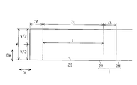
- a slit process is performed in which the deposition mask substrate 1 is cut in the entire width direction DW (full width), and measurement is performed as a part of the deposition mask substrate 1 in the longitudinal direction DL.
- the base material 2M for cutting is cut out.
- the dimension W in the width direction DW of the measurement substrate 2M is equal to the dimension in the width direction DW of the deposition mask substrate 1.
- the height at each position in the longitudinal direction DL is measured for the surface 2S of the measurement base material 2M.
- the measurement range ZL which is a range in which the height at each position in the longitudinal direction DL is measured, is a range excluding the non-measurement range ZE that is both ends of the measurement base material 2M in the longitudinal direction DL.
- the length in the longitudinal direction DL of each non-measurement range ZE is a range having a possibility of having a wave shape different from that of the vapor deposition mask substrate 1 by a slitting process for cutting the vapor deposition mask substrate 1.
- Each non-measurement range ZE has a length in the longitudinal direction DL of, for example, 100 mm.
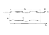
- FIG. 3 is a graph showing an example of the height of each position of the measurement base material 2M in the longitudinal direction DL, and shows the height along with the cross-sectional structure of the cross section including the longitudinal direction DL of the measurement base material 2M. It is.
- the positions in the longitudinal direction DL at which the height is measured are arranged at intervals at which the corrugated irregularities of the vapor deposition mask substrate 1 can be copied.
- the positions in the longitudinal direction DL at which the height is measured are arranged at intervals of 1 mm in the longitudinal direction DL, for example.
- the length of the broken line LC connecting the heights of the respective positions in the longitudinal direction DL is calculated as the surface distance L.
- the elongation difference rate of the deposition mask substrate 1 is determined by Equation 1.
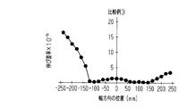
- FIG. 4 shows the elongation difference rate at each position in the width direction DW of the vapor deposition mask substrate 1.
- the solid line shown in the upper part of FIG. 4 is an example in which the elongation difference rate of the central part in the width direction DW is larger than the other parts, and the solid line shown in the lower part of FIG. This is an example in which the rate is larger than other portions.
- the elongation difference rate of the vapor deposition mask substrate 1 has a maximum value at the center portion RC in the width direction DW and has a minimum value near the boundary between the center portion RC and the end portion RE. .
- the elongation difference rate of the base material 1 for vapor deposition masks increases toward both ends RE of the width direction DW from the center part RC.
- the center portion RC in the width direction DW has the center PC in the width direction DW of the vapor deposition mask substrate 1 as the center in the width direction DW of the center portion RC.
- the length in the width direction DW which the center part RC of the width direction DW has is 40% of the length in the width direction DW which the base material 1 for vapor deposition masks has.
- the length in the width direction DW which each edge part RE of the width direction DW has is 30% of the length in the width direction DW which the base material 1 for vapor deposition masks has.
- Such elongation difference rate of the substrate 1 for vapor deposition mask satisfies the following three conditions.
- the elongation difference rate of at least one of both end portions RE is smaller than the elongation difference rate of the central portion RC in the width direction DW.
- the elongation difference of the central portion RC is 3 ⁇ 10 ⁇ 5 or less.
- the elongation difference ratio of both end portions RE is 15 ⁇ 10 ⁇ 5 or less. Note that the elongation difference ratio of both end portions RE is preferably 10 ⁇ 10 ⁇ 5 or less.
- the central portion RC As shown by the solid line in the upper stage of FIG. 4, as an example satisfying the condition 1, in the deposition mask substrate 1 in which the elongation difference rate at each end RE is smaller than the elongation difference rate at the central portion RC, the central portion RC The number of the unevenness on the surface of the surface and the step on the surface of the central portion RC are larger than each end portion RE.
- the liquid supplied to the surface of the deposition mask substrate 1 is transferred from the central portion RC to each end RE, and from each end RE to the outside of the deposition mask substrate 1. Easy to flush.
- the vapor deposition mask substrate 1 As shown in the lower solid line in FIG. 4, as another example that satisfies the condition 1, in the vapor deposition mask substrate 1, only the elongation difference rate at one end RE is smaller than the elongation difference rate at the central portion RC. The number of the unevenness on the surface of one end RE and the step difference on the surface of one end RE are larger than those of the central portion RC and the other end RE. In such a deposition mask substrate 1, the liquid supplied to the surface of the deposition mask substrate 1 is transferred from one end RE to the other end RE, and from the other end RE to the deposition mask substrate. Easy to flow outside of 1.
- the liquid supplied to the surface of the vapor deposition mask substrate 1 is, for example, a developer for developing the resist layer located on the surface of the vapor deposition mask substrate 1 and a cleaning liquid for removing the developer from the surface. .
- the liquid supplied to the surface of the evaporation mask substrate 1 is, for example, an etching solution for etching the evaporation mask substrate 1 and a cleaning solution for removing the etching solution from the surface.
- the liquid supplied to the surface of the deposition mask substrate 1 is, for example, a stripping solution for stripping the resist layer remaining after etching on the surface of the deposition mask substrate 1 and removing the stripping solution from the surface. This is a cleaning solution.
- the vapor deposition mask base material 1 in which the elongation difference rate at each end RE is larger than the elongation difference rate at the central portion RC it is supplied to the surface of the vapor deposition mask base material 1.
- the liquid easily flows from each end RE to the outside of the vapor deposition mask substrate 1, but also easily flows from each end RE to the central portion RC.
- a liquid puddle is likely to be generated in the central portion RC, and the processing uniformity using the treatment with the liquid becomes a factor in the surface of the vapor deposition mask substrate 1.
- the configuration satisfying the condition 1 and the effect obtained thereby are obtained by the difference between the elongation difference rate at the central portion RC and the elongation difference rate at each end portion RE. It is derived for the first time by recognizing the problem in processing.
- FIG. 5 is a plan view showing a schematic planar structure of a mask device provided with a vapor deposition mask manufactured using the vapor deposition mask substrate 1.
- FIG. 6 is a cross-sectional view illustrating an example of a cross-sectional structure of the mask portion included in the vapor deposition mask
- FIG. 7 is a cross-sectional view illustrating another example of the cross-sectional structure of the mask portion included in the vapor deposition mask.
- the quantity of the vapor deposition mask with which a mask apparatus is equipped, and the quantity of the mask part with which the vapor deposition mask 30 is provided are examples.
- the mask device 10 includes a main frame 20 and three vapor deposition masks 30.
- the main frame 20 has a rectangular frame shape that supports a plurality of vapor deposition masks 30 and is attached to a vapor deposition apparatus for performing vapor deposition.
- the main frame 20 has a main frame hole 21 penetrating the main frame 20 over almost the entire range where each vapor deposition mask 30 is located.
- Each vapor deposition mask 30 includes a plurality of frame portions 31 having a strip shape and three mask portions 32 in each frame portion 31.
- the frame portion 31 has a strip shape that supports the mask portion 32 and is attached to the main frame 20.
- the frame portion 31 has a frame hole 33 penetrating the frame portion 31 over substantially the entire range where the mask portion 32 is located.
- the frame part 31 has a higher rigidity than the mask part 32 and has a frame shape surrounding the frame hole 33.
- Each mask part 32 is fixed to the frame inner edge part of the frame part 31 that divides the frame hole 33 one by one by welding or adhesion.
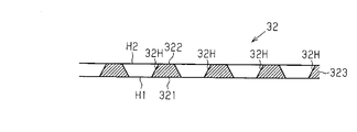
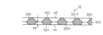
- an example of the mask unit 32 includes a mask plate 323.
- the mask plate 323 may be a single plate member formed from the vapor deposition mask substrate 1 or a laminate of one plate member and a resin plate formed from the vapor deposition mask substrate 1. There may be.
- the mask plate 323 includes a first surface 321 and a second surface 322 that is a surface opposite to the first surface 321.
- the first surface 321 faces a deposition target such as a glass substrate in a state where the mask device 10 is attached to the deposition device.
- the second surface 322 faces the vapor deposition source of the vapor deposition apparatus.
- the mask portion 32 has a plurality of holes 32 ⁇ / b> H that penetrate the mask plate 323.
- the wall surface of the hole 32H is inclined with respect to the thickness direction of the mask plate 323 in a sectional view.
- the shape of the wall surface of the hole 32H may be a straight line shape as shown in FIG. 6 in a cross-sectional view, may be a semicircular arc shape protruding toward the outside of the hole 32H, or a plurality of bending points. It may be a complicated curved line having
- the thickness of the mask plate 323 is 1 ⁇ m or more and 50 ⁇ m or less, preferably 2 ⁇ m or more and 20 ⁇ m or less. If the thickness of the mask plate 323 is 50 ⁇ m or less, the depth of the hole 32H formed in the mask plate 323 can be 50 ⁇ m or less. Thus, if the mask plate 323 is thin, the area of the wall surface of the hole 32H itself is reduced, and the amount of the vapor deposition material adhering to the wall surface of the hole 32H is reduced.
- the second surface 322 includes a second opening H2 that is an opening of the hole 32H
- the first surface 321 includes a first opening H1 that is an opening of the hole 32H.
- the second opening H2 is larger than the first opening H1 in plan view.
- Each hole 32H is a passage through which the vapor deposition material sublimated from the vapor deposition source passes, and the vapor deposition material sublimated from the vapor deposition source travels from the second opening H2 toward the first opening H1. If the second opening H2 is the hole 32H larger than the first opening H1, the amount of the vapor deposition material entering the hole 32H from the second opening H2 can be increased.
- the area of the hole 32H in the cross section along the first surface 321 may monotonously increase from the first opening H1 to the second opening H2 from the first opening H1 toward the second opening H2.
- the mask portion 32 has a plurality of holes 32H that penetrate the mask plate 323.
- the second opening H2 is larger than the first opening H1 in plan view.
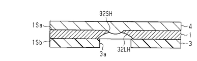
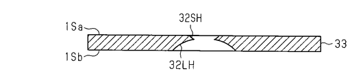
- the hole 32H includes a large hole 32LH having a second opening H2 and a small hole 32SH having a first opening H1.
- the cross-sectional area of the large hole 32LH monotonously decreases from the second opening H2 toward the first surface 321.
- the cross-sectional area of the small hole 32SH monotonously decreases from the first opening H1 toward the second surface 322.
- the wall surface of the hole 32H has a shape protruding toward the inside of the hole 32H at a portion where the large hole 32LH and the small hole 32SH are connected, that is, in the middle of the thickness direction of the mask plate 323 in a cross-sectional view.
- the distance between the portion protruding from the wall surface of the hole 32H and the first surface 321 is the step height SH.
- the step height SH is zero. From the viewpoint of easily ensuring the amount of the vapor deposition material that reaches the first opening H1, a configuration in which the step height SH is zero is preferable.
- the mask plate 323 is thin enough to form the hole 32H by wet etching from one side of the vapor deposition mask substrate 1, for example, 50 ⁇ m or less. It is.
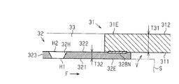
- FIG. 8 shows an example of a cross-sectional structure of the joint structure between the mask portion 32 and the frame portion 31.
- FIG. 9 shows another example of the cross-sectional structure of the joint structure between the mask portion 32 and the frame portion 31.
- the outer edge portion 32E of the mask plate 323 is a region not provided with the hole 32H.
- a portion included in the outer edge portion 32E of the mask plate 323 is an example of a side surface provided in the mask portion, and is joined to the frame portion 31.
- the frame portion 31 includes an inner edge portion 31E that partitions the frame hole 33.
- the inner edge portion 31 ⁇ / b> E includes a bonding surface 311 that faces the mask plate 323 and a non-bonding surface 312 that is a surface opposite to the bonding surface 311.
- the thickness T31 of the inner edge portion 31E that is, the distance between the joint surface 311 and the non-joint surface 312 is sufficiently thicker than the thickness T32 of the mask plate 323, whereby the frame portion 31 has higher rigidity than the mask plate 323.
- the frame part 31 has high rigidity with respect to the inner edge part 31 ⁇ / b> E depending on its own weight or the inner edge part 31 ⁇ / b> E being displaced toward the mask part 32.
- the joint surface 311 of the inner edge portion 31E includes a joint portion 32BN joined to the second surface 322.
- the joint portion 32BN is located continuously or intermittently over substantially the entire circumference of the inner edge portion 31E.
- the joining portion 32BN may be a welding mark formed by welding the joining surface 311 and the second surface 322, or may be a joining layer that joins the joining surface 311 and the second surface 322.
- the frame portion 31 joins the joint surface 311 of the inner edge portion 31E and the second surface 322 of the mask plate 323, and applies a stress F to the mask plate 323 so that the mask plate 323 is pulled outward.
- the frame 31 is also applied by the main frame 20 with a stress that is pulled toward the outside thereof to the same extent as the stress F on the mask plate 323.
- the stress due to the joining between the main frame 20 and the frame portion 31 is released, and the stress F applied to the mask plate 323 is also relaxed.
- the position of the joint portion 32BN on the joint surface 311 is preferably a position where the stress F isotropically acts on the mask plate 323, and is appropriately selected based on the shape of the mask plate 323 and the shape of the frame hole 33. Is done.
- the joint surface 311 is a plane on which the joint portion 32BN is located, and extends from the outer edge portion 32E of the second surface 322 toward the outside of the mask plate 323.
- the inner edge portion 31E has a surface structure in which the second surface 322 is pseudo-expanded to the outside thereof, and extends from the outer edge portion 32E of the second surface 322 toward the outside of the mask plate 323. Therefore, a space V corresponding to the thickness of the mask plate 323 is easily formed around the mask plate 323 in a range where the bonding surface 311 is widened. As a result, it is possible to suppress physical interference between the deposition target S and the frame portion 31 around the mask plate 323.
- the outer edge portion 32E of the second surface 322 includes a region where the hole 32H is not formed.
- the outer edge portion 32E of the second surface 322 is joined to the joining surface 311 included in the frame portion 31 through joining by the joining portion 32BN.
- the frame portion 31 applies a stress F to the mask plate 323 so that the mask plate 323 is pulled outward, and the space V corresponding to the thickness of the mask plate 323 in a range where the joint surface 311 extends.
- FIG. 10 shows an example of the relationship between the number of holes 32H provided in the vapor deposition mask 30 and the number of holes 32H provided in the mask unit 32.
- FIG. 11 shows another example of the relationship between the number of holes 32H provided in the vapor deposition mask 30 and the number of holes 32H provided in the mask portion 32.
- the frame portion 31 has three frame holes 33.
- the vapor deposition mask 30 includes one mask portion 32 for each frame hole 33.
- the inner edge portion 31E that defines the frame hole 33A is joined to one mask portion 32A, and the inner edge portion 31E that defines the frame hole 33B is joined to the other one mask portion 32B to define the frame hole 33C.
- 31E is joined to another one mask portion 32C.
- the vapor deposition mask 30 is repeatedly used for a plurality of vapor deposition targets. For this reason, each hole 32H provided in the vapor deposition mask 30 is required to have high accuracy in the position of the hole 32H, the structure of the hole 32H, and the like. As shown in FIG. 10, if the number of holes 32 ⁇ / b> H required for one frame portion 31 is divided and carried by the three mask portions 32, it is transformed into a part of one mask portion 32. Even if this occurs, a new mask part that is replaced with a deformed mask part 32 in comparison with the configuration in which the number of holes 32H required for one frame part 31 is carried by a single mask part. The size of 32 can be reduced.
- the inspection regarding the position of the hole 32H and the structure of the hole 32H is preferably performed in a state where the stress F is applied, that is, in a state where the mask portion 32 is bonded to the frame portion 31.
- the above-described joint portion 32BN preferably has a configuration that enables the deformed mask portion 32 to be replaced with a new mask portion 32. And the yield of the mask part 32 falls, so that the thickness of the mask board 323 which comprises the mask part 32 is thin, and the hole 32H is small. Therefore, the configuration in which one mask portion 32 is provided for each frame hole 33 is also particularly suitable for the vapor deposition mask 30 in which high definition is required for the mask portion 32.
- the frame portion 31 has three frame holes 33.
- the vapor deposition mask 30 includes one mask portion 32 that is common to each frame hole 33.
- the inner edge portion 31E that defines the frame hole 33A, the inner edge portion 31E that defines the frame hole 33B, and the inner edge portion 31E that defines the frame hole 33C are joined to one common mask portion 32.
- the number of holes 32H required for one frame portion 31 is configured to be handled by one mask portion 32, the number of mask portions 32 bonded to the frame portion 31 can be one. Therefore, it is possible to reduce the load required for joining the frame part 31 and the mask part 32.
- the yield of the mask portion 32 is likely to increase as the thickness of the mask plate 323 constituting the mask portion 32 increases and the size of the hole 32H increases. Therefore, the configuration including the mask portion 32 common to each frame hole 33 is also suitable for the vapor deposition mask 30 in which the mask portion 32 is required to have a low resolution.
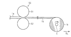
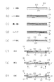
- FIG. 12 and FIG. 13 show an example of manufacturing by using rolling as a method for manufacturing a base material for a vapor deposition mask.
- a base material 1a formed from invar or the like and extending in the longitudinal direction DL is prepared.
- the base material 1a is transported toward a rolling device 50 including a pair of rolling rollers 51 and 52 so that the longitudinal direction DL of the base material 1a is parallel to the transport direction in which the base material 1a is transported.
- the base material 1 a reaches between the pair of rolling rollers 51 and 52, the base material 1 a is rolled by the pair of rolling rollers 51 and 52.
- the base material 1a is extended in the longitudinal direction DL, whereby the rolled material 1b can be obtained.
- the rolled material 1b may be handled in a state where the rolled material 1b is stretched into a band shape without being wound around the core C.
- the thickness of the rolled material 1b is, for example, 10 ⁇ m or more and 50 ⁇ m or less.
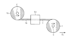
- the rolled material 1b is annealed using an annealing device 53. Thereby, the base material 1 for vapor deposition masks is obtained. Since annealing of the rolled material 1b is performed while pulling the rolled material 1b in the longitudinal direction DL, it is possible to obtain the deposition mask base material 1 in which the residual stress is reduced as compared with the rolled material 1b before annealing.
- Each of the rolling process and the annealing process may be changed as follows. That is, for example, in the rolling process, a rolling device including a plurality of pairs of rolling rollers may be used.
- the base material 1 for vapor deposition masks may be manufactured by repeating a rolling process and an annealing process in multiple times. Further, in the annealing process, the rolling material 1b may be performed on the rolled material 1b wound around the core C instead of being pulled in the longitudinal direction DL.
- the deposition mask base material 1 after the annealing is obtained by winding the deposition mask base material 1 around the core C.
- the substrate 1 for vapor deposition mask may be wrinkled by warping according to the diameter when it is wound around the core C. Therefore, depending on the size of the diameter when the vapor deposition mask substrate 1 is wound around the core C and the material forming the base material 1a, it is preferable to anneal the rolled material 1b while pulling the rolled material 1b in the longitudinal direction DL. .
- the deposition mask substrate 1 When electrolysis is used in the method for manufacturing the deposition mask substrate 1, the deposition mask substrate 1 is formed on the electrode surface used for electrolysis, and then the deposition mask substrate 1 is released from the electrode surface. .
- the electrolytic bath used for electrolysis includes an iron ion supply agent, a nickel ion supply agent, and a pH buffer.
- the electrolytic bath used for electrolysis may contain a stress relaxation agent, an Fe 3+ ion mask agent, a complexing agent such as malic acid or citric acid, and the like, and is a weakly acidic solution adjusted to a pH suitable for electrolysis.
- iron ion supply agent examples include ferrous sulfate heptahydrate, ferrous chloride, and iron sulfamate.
- the nickel ion supply agent is, for example, nickel sulfate (II), nickel chloride (II), nickel sulfamate, or nickel bromide.
- Examples of the pH buffer are boric acid and malonic acid. Malonic acid also functions as an Fe 3+ ion masking agent.
- the stress relaxation agent is, for example, saccharin sodium.
- the electrolytic bath used for the electrolysis is, for example, an aqueous solution containing the above-described additives, and is adjusted so that the pH becomes, for example, 2 or more and 3 or less by a pH adjuster such as 5% sulfuric acid or nickel carbonate. .
- the electrolysis conditions used for electrolysis are conditions in which the thickness of the deposition mask substrate 1, the composition ratio in the deposition mask substrate 1, and the like are adjusted by the temperature of the electrolytic bath, the current density, and the electrolysis time.
- the anode in the electrolysis conditions using the above-described electrolytic bath is, for example, pure iron and nickel.
- the cathode under electrolysis conditions is, for example, a stainless plate such as SUS304.
- the temperature of the electrolytic bath is, for example, 40 ° C. or more and 60 ° C. or less.
- the current density is, for example, 1 A / dm 2 or more and 4 A / dm 2 or less. At this time, the current density on the electrode surface is set so that the above-described conditions 1, 2, and 3 are satisfied.
- the deposition mask substrate 1 obtained by electrolysis or the deposition mask substrate 1 obtained by rolling may be thinly processed by chemical polishing or thinly processed by electrical polishing. Also good.
- the polishing liquid used for chemical polishing is, for example, a chemical polishing liquid for iron-based alloys containing hydrogen peroxide as a main component.
- the electrolytic solution used for electrical polishing is a perchloric acid type electrolytic polishing solution or a sulfuric acid type electrolytic polishing solution.
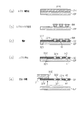
- a process for manufacturing the mask portion 32 shown in FIG. 7 will be described with reference to FIGS.
- the process for manufacturing the mask portion 32 described with reference to FIG. 6 is a process for manufacturing the mask portion 32 described with reference to FIG. 7 in order to form the large hole 32LH with the small hole 32SH as a through hole. Since it is the same as the process which omitted the process of, the overlapping description is omitted.
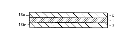
- a deposition mask substrate 1 including a first surface 1Sa and a second surface 1Sb, and a first dry film resist 2 attached to the first surface 1Sa.
- a second dry film resist 3 to be attached to the second surface 1Sb.
- Each of the two dry film resists 2 and 3 is a film formed separately from the vapor deposition mask substrate 1.
- the first dry film resist 2 is attached to the first surface 1Sa
- the second dry film resist 3 is attached to the second surface 1Sb.
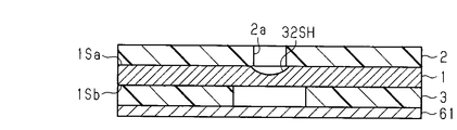
- portions of the dry film resists 2 and 3 other than the portions where the holes are formed are exposed, and the exposed dry film resist is developed.
- the first through hole 2 a is formed in the first dry film resist 2
- the second through hole 3 a is formed in the second dry film resist 3.
- the second dry film resist 3 When the second dry film resist 3 is exposed, light is irradiated to a portion other than the portion where the second through hole 3a is formed on the surface of the second dry film resist 3 opposite to the surface in contact with the vapor deposition mask substrate 1. Put the original plate configured to reach. Further, when developing the exposed dry film resist, for example, a sodium carbonate aqueous solution is used as the developer. At this time, since the above-described conditions 1, 2, and 3 are satisfied, variations in the surface of the vapor deposition mask substrate 1 can be suppressed with respect to the results of development with the developer and the results of cleaning with the cleaning solution. As a result, it is possible to improve the uniformity within the surface of the evaporation mask substrate 1 with respect to the shape and size of the first through hole 2a and the shape and size of the second through hole 3a.
- the first surface 1Sa of the evaporation mask substrate 1 is etched using a ferric chloride solution using the first dry film resist 2 as a mask.
- the second protective layer 61 is formed on the second dry film resist 3 so that the second surface 1Sb of the deposition mask substrate 1 is not etched simultaneously with the first surface 1Sa.
- the material for forming the second protective layer 61 may be any material that is difficult to be etched by the ferric chloride solution.
- a small hole 32SH that is recessed toward the second surface 1Sb is formed in the first surface 1Sa of the evaporation mask substrate 1 via the first through hole 2a of the first dry film resist 2.
- the small hole 32SH has a first opening H1 that opens in the first surface 1Sa.
- the etching solution for etching the deposition mask substrate 1 is an acidic etching solution, and when the deposition mask substrate 1 is made of invar, the etching solution can etch the invar. Good.
- Acidic etchants are, for example, perchloric acid, hydrochloric acid, sulfuric acid, formic acid, and ferric perchlorate solution and a mixture of ferric perchlorate solution and ferric chloride solution. A solution in which any one of acetic acid is mixed.
- the method for etching the deposition mask substrate 1 may be a dip method in which the deposition mask substrate 1 is immersed in an acidic etching solution, or a spray method in which an acidic etching solution is sprayed onto the deposition mask substrate 1. It may be.
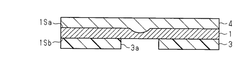
- the first dry film resist 2 formed on the first surface 1Sa of the vapor deposition mask substrate 1 and the second protective layer 61 in contact with the second dry film resist 3 are removed.
- the 1st protective layer 4 for preventing the etching of 1st surface 1Sa is formed in 1st surface 1Sa of the base material 1 for vapor deposition masks.
- the formation material of the 1st protective layer 4 should just be a material which is hard to be etched with a ferric chloride liquid.
- the second surface 1Sb of the deposition mask substrate 1 is etched using a ferric chloride solution using the second dry film resist 3 as a mask.
- a large hole 32LH that is recessed toward the first surface 1Sa is formed in the second surface 1Sb of the vapor deposition mask substrate 1 through the second through hole 3a of the second dry film resist 3.
- the large hole 32LH has a second opening H2 that opens to the second surface 1Sb, and the second opening H2 is larger than the first opening H1 in a plan view facing the second surface 1Sb.
- etching solution used at this time is also an acidic etching solution, and when the vapor deposition mask substrate 1 is made of invar, any etching solution that can etch invar may be used.
- the method for etching the vapor deposition mask substrate 1 may also be a dip type in which the vapor deposition mask substrate 1 is immersed in an acidic etching solution, or a spray that sprays an acidic etching solution on the vapor deposition mask substrate 1. It may be a formula.
- a deoxidizer such as granular aluminum or magnesium is mixed into the material for forming the base material.
- Aluminum and magnesium are contained in the base material as metal oxides such as aluminum oxide and magnesium oxide. Most of these metal oxides are removed from the base material before the base material is rolled. On the other hand, a part of the metal oxide remains in the base material to be rolled. In this regard, according to the manufacturing method using electrolysis for manufacturing the deposition mask substrate 1, the metal oxide is prevented from being mixed into the mask portion 32.
- Method of manufacturing vapor deposition mask Each example of the manufacturing method of a vapor deposition mask is demonstrated. An example using a method of forming holes by wet etching will be described with reference to FIG. In addition, an example using a method of forming holes by electrolysis will be described with reference to FIG. 21, and another example using a method of forming holes by electrolysis will be described with reference to FIG. Moreover, the method of manufacturing the vapor deposition mask using the mask part 32 demonstrated in FIG. 6 and the method of manufacturing the vapor deposition mask provided with the mask part 32 demonstrated in FIG. 7 are the forms of the etching performed with respect to the base material 32K. However, the other steps are almost the same. Below, the manufacturing method of the vapor deposition mask provided with the mask part 32 demonstrated in FIG. 6 is mainly demonstrated, and the duplicate description is abbreviate
- a base material 32K is prepared (see FIG. 20A).
- the base material 32K preferably further includes a support SP for supporting the vapor deposition mask base material 1 in addition to the above-described vapor deposition mask base material 1 processed as the mask plate 323.
- the first surface 321 of the base material 32K corresponds to the above-described first surface 1Sa
- the second surface 322 of the base material 32K corresponds to the above-described second surface 1Sb.
- a resist layer PR is formed on the second surface 322 of the base material 32K (see FIG. 20B), and the resist layer PR is exposed and developed, whereby the resist mask RM is formed on the second surface 322. Is formed (see FIG. 20C).
- a hole 32H is formed in the base material 32K by wet etching from the second surface 322 using the resist mask RM (see FIG. 20D).
- a second opening H2 is formed on the second surface 322 where wet etching is started, and a first opening smaller than the second opening H2 is formed on the first surface 321 where etching is performed later than that. H1 is formed.
- the mask portion 32 described above is manufactured by removing the resist mask RM from the second surface 322 (see FIG. 20E). Finally, the outer edge portion 32E of the second surface 322 is joined to the inner edge portion 31E of the frame portion 31, and the support SP is released from the mask portion 32, whereby the vapor deposition mask 30 is manufactured (FIG. 20F). ) To (h)).
- the small hole 32SH is formed.
- a resist or the like for protecting the small holes 32SH is filled in the small holes 32SH.
- the above-described process is performed on the surface of the base material 32 ⁇ / b> K corresponding to the second surface 322, whereby the mask portion 32 is manufactured.
- resistance welding is used as a method for joining the outer edge portion 32E of the second surface 322 to the inner edge portion 31E of the frame portion 31.
- a plurality of holes SPH are formed in the insulating support SP.
- Each hole SPH is formed in the part which opposes the part used as junction part 32BN in support SP.
- an intermittent joint portion 32BN is formed by energization through the hole SPH, thereby the outer edge portion 32E and the inner edge portion 31E. Welds.
- laser welding is used as a method of joining the outer edge portion 32E of the second surface 322 to the inner edge portion 31E of the frame portion 31.
- a support SP having optical transparency is used, and laser light is irradiated through the support SP to a portion to be the joint portion 32BN.
- intermittent junction part 32BN is formed by irradiating intermittent laser beam, or continuous junction part 32BN is formed by continuing irradiating laser beam continuously, and thereby
- the outer edge portion 32E and the inner edge portion 31E are welded. Note that, when the support SP supports the mask portion 32 in a state in which stress toward the outside of the mask portion 32 is applied, the application of stress to the mask portion 32 is omitted in this welding. It is also possible.
- ultrasonic welding is used as a method of joining the outer edge portion 32E of the second surface 322 to the inner edge portion 31E of the frame portion 31.
- the outer edge portion 32E and the inner edge portion 31E are sandwiched by the clamp CP or the like, and an ultrasonic wave is applied to a portion that becomes the joint portion 32BN.
- the member to which the ultrasonic wave is directly applied may be the frame part 31 or the mask part 32.
- a crimp mark by the clamp CP is formed on the frame portion 31 and the support SP.
- the vapor deposition mask described with reference to FIGS. 8 and 9 is manufactured by another example shown in FIGS. 21A to 21E or another example shown in FIGS. 22A to 22F. It is also possible.
- a resist layer PR is formed on the electrode surface EPS which is the surface of the electrode EP used for electrolysis.
- a resist mask RM that is an example of a pattern is formed on the electrode surface EPS by performing exposure and development on the resist layer PR (see FIG. 21B).
- the resist mask RM has an inverted frustum shape whose top is located on the electrode surface EPS in a cross section orthogonal to the electrode surface EPS, and the area in the cross section along the electrode surface EPS increases as the distance from the electrode surface EPS increases. Has a large shape.
- electrolysis using the electrode surface EPS having the resist mask RM is performed, and a metal plate extending in a region other than the resist mask RM in the electrode surface EPS is formed as the mask portion 32 (see FIG. 21C). ).
- a hole having a shape following the shape of the resist mask RM is formed in the metal plate.
- the hole 32H of the mask portion 32 is formed in a self-aligning manner. That is, the surface in contact with the electrode surface EPS functions as the first surface 321 having the first opening H1, and the outermost surface having the second opening H2, which is an opening larger than the first opening H1, serves as the second surface 322. Function.
- the joint surface 311 of the inner edge portion 31E is joined to the outer edge portion 32E of the second surface 322 having the second opening H2, and then the stress for peeling the mask portion 32 from the electrode surface EPS is applied to the frame portion 31.
- the mask portion 32 bonded to the support or the like is peeled off from the electrode surface EPS, and the bonding surface 311 of the inner edge portion 31E is bonded to the outer edge portion 32E of the second surface 322 of the mask portion 32.
- the vapor deposition mask 30 in a state where the mask portion 32 is bonded to the frame portion 31 is manufactured (see FIG. 21E).
- a resist layer PR is formed on the electrode surface EPS used for electrolysis (FIG. 22A). reference).
- a resist mask RM which is an example of a pattern, is formed on the electrode surface EPS (see FIG. 22B).
- the resist mask RM has a frustum shape whose bottom is located on the electrode surface EPS in a cross section orthogonal to the electrode surface EPS, and the area of the cross section along the electrode surface EPS increases as the distance from the electrode surface EPS increases. Has a small shape.
- electrolysis is performed using the electrode surface EPS having the resist mask RM, and a metal plate extending in a region other than the resist mask RM in the electrode surface EPS is formed as the mask portion 32 (FIG. 22C). reference).
- a hole having a shape following the shape of the resist mask RM is formed in the metal plate.
- the hole 32H in the mask part 32 is formed in a self-aligning manner. That is, the surface in contact with the electrode surface EPS functions as the second surface 322 having the second opening H2, and the outermost surface having the first opening H1, which is an opening smaller than the second opening H2, is the first surface 321. Function.
- the joining surface 311 of the inner edge portion 31E is joined to the outer edge portion 32E of the second surface 322 having the second opening H2, and then the intermediate transfer base material TM is peeled off from the mask portion 32. Thereby, the vapor deposition mask 30 in a state where the mask portion 32 is bonded to the frame portion 31 is manufactured (see FIG. 22F).
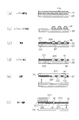
- Example 1 Each embodiment will be described with reference to FIGS.
- the base material 1a made of invar is subjected to a rolling step and a slit step for cutting the metal plate so that a desired size is obtained in the width direction DW from the rolled metal plate.
- the base material 1 for the vapor deposition mask of Example 1 in which the length in the width direction DW is 500 mm and the thickness is 20 ⁇ m is manufactured by manufacturing the rolled material 1b and subjecting the rolled material 1b to an annealing process. Obtained.
- the measurement base material 2 ⁇ / b> M of Example 1 having a length in the longitudinal direction DL of 700 mm was cut out from the deposition mask base material 1 of Example 1. Subsequently, the surface distance L of the cut-out measurement substrate 2M was measured over the entire width direction DW of the measurement substrate 2M, and the elongation difference rate in the measurement substrate 2M of Example 1 was obtained. At this time, the following conditions were used as measurement conditions for the surface distance L.
- Measuring device CNC image measurement system VMR-6555 manufactured by Nikon Corporation Length in the longitudinal direction DL of the measurement range ZL: 500 mm Length in the longitudinal direction DL of the non-measurement range ZE: 100 mm Measurement interval in the longitudinal direction DL: 1 mm Measurement interval in the width direction DW: 20 mm
- the measurement results of the elongation difference rate of Example 1 are shown in FIG.
- the elongation difference rate which Table 1 shows is the maximum value in center part RC and each edge part RE.
- the maximum value of the elongation difference ratio with the central portion RC of the first embodiment it is 2.42 ⁇ 10 -5 or less
- elongation Saritsu having each end RE is, 10 ⁇ 10 - 5 or less, and it was confirmed that the above conditions 2 and 3 were satisfied.
- Example 1 the maximum value of the elongation difference rate at one end (end A) of both ends RE in the width direction DW is 4.56 ⁇ 10 ⁇ 5 .
- the maximum value of the differential elongation at the other (end B) of both ends RE in the width direction DW is 1.53 ⁇ 10 ⁇ 5 which is larger than the differential elongation, and is the center of the width direction DW. It was recognized that it was smaller than the elongation difference rate at the portion RC. That is, it was recognized that the above condition 1 was satisfied.
- the difference in the maximum value of the elongation difference at each end RE in the width direction DW was 3.03 ⁇ 10 ⁇ 5 .
- Example 2 By setting the pressing force between the rolling rollers 51 and 52 higher than that in Example 1 and setting other conditions in the same manner as in Example 1, the length in the width direction DW is 500 mm, and the thickness The base material 1 for vapor deposition masks of Example 2 which is 15 micrometers was obtained. Next, as in Example 1, the measurement base material 2M was cut out from the vapor deposition mask base material 1 in Example 2, and the surface distance L of the cut out measurement base material 2M was determined in the width direction of the measurement base material 2M. Measured over the entire DW, the elongation difference in the measurement base material 2M of Example 2 was obtained.
- Example 2 The measurement results of the differential elongation of Example 2 are shown in FIG. As shown in FIG. 25, the maximum value of the elongation difference ratio of the central portion RC of Example 2 is 0.75 ⁇ 10 ⁇ 5 , and the maximum value of the elongation difference ratio of each end portion RE is 0. It was found to be 10 ⁇ 10 ⁇ 5 and 0.68 ⁇ 10 ⁇ 5 . And in Example 2, the elongation difference rate of both edge part RE of the width direction DW is smaller than the elongation difference rate in the center part RC of the width direction DW, and the said conditions 1, 2, and 3 are satisfy
- Example 3 The pressing force between the rolling rollers 51 and 52 is set higher than that in the first embodiment, and the distribution is different from that in the second embodiment, and other conditions are set in the same manner as the conditions in the first embodiment.
- the vapor deposition mask substrate 1 of Example 3 having a length of 500 mm and a thickness of 15 ⁇ m was obtained.
- the measurement base material 2M was cut out from the vapor deposition mask base material 1 in Example 3, and the surface distance L of the cut out measurement base material 2M was determined in the width direction of the measurement base material 2M. Measured over the entire DW, the elongation difference rate in the measurement base material 2M of Example 3 was obtained.
- the measurement results of the elongation difference rate of Example 3 are shown in FIG. As shown in FIG. 26, the maximum value of the elongation difference ratio with the central portion RC of Example 3, at 1.23 ⁇ 10 -5 or less, elongation Saritsu having each end RE is, 15 ⁇ 10 - 5 or less, and it was confirmed that the above conditions 2 and 3 were satisfied.
- Example 3 the maximum value of the elongation difference rate at one of the end portions RE in the width direction DW (end portion B) is 1.11 ⁇ 10 ⁇ 5 ,
- the maximum value of the differential elongation at the other (end A) of both end portions RE in the width direction DW is 12.50 ⁇ 10 ⁇ 5 which is smaller than the differential expansion rate, and is It was recognized that it was larger than the differential elongation. That is, it was recognized that the above condition 1 was satisfied.
- the difference in the maximum value of the elongation difference at each end RE in the width direction DW was 11.39 ⁇ 10 ⁇ 5 .
- the measurement results of the elongation difference rate of Comparative Example 1 are shown in FIG. As shown in FIG. 27, the maximum value of the elongation difference ratio of the central portion RC of Comparative Example 1 is 9.68 ⁇ 10 ⁇ 5 , and the elongation difference ratio of each end portion RE is 15 ⁇ 10 ⁇ 5. It was recognized that the above condition 2 was not satisfied. In Comparative Example 1, the elongation difference rate at both ends RE in the width direction DW was larger than the elongation difference rate at the center portion RC in the width direction DW, and it was also recognized that the above condition 1 was not satisfied. .
- Comparative Example 2 By changing the distribution of the pressing force between the rolling rollers 51 and 52 from Comparative Example 1 and setting other conditions in the same manner as in Comparative Example 1, the length in the width direction DW is 500 mm, and The base material 1 for vapor deposition masks of the comparative example 2 whose thickness is 20 micrometers was obtained. Next, in the same manner as in Comparative Example 1, the measurement base material 2M is cut out from the vapor deposition mask base material 1 in Comparative Example 2, and the surface distance L of the cut out measurement base material 2M is determined in the width direction of the measurement base material 2M. Measured over the entire DW, the elongation difference rate in the measurement base material 2M of Comparative Example 2 was obtained.
- the measurement results of the differential elongation of Comparative Example 2 are shown in FIG. As shown in FIG. 28, the maximum value of the elongation difference ratio of the central portion RC of Comparative Example 2 is 19.66 ⁇ 10 ⁇ 5 , and the elongation difference of one of the end portions RE (the end portion A). The rate was 15 ⁇ 10 ⁇ 5 or more, and it was confirmed that the above conditions 2 and 3 were not satisfied.
- Comparative Example 3 By changing the distribution of the pressing force between the rolling rollers 51 and 52 from Comparative Example 1 and setting other conditions in the same manner as in Comparative Example 1, the length in the width direction DW is 500 mm, and The base material 1 for vapor deposition masks of the comparative example 3 whose thickness is 20 micrometers was obtained. Next, as in Comparative Example 1, the measurement base material 2M is cut out from the vapor deposition mask base material 1 in Comparative Example 3, and the surface distance L of the cut out measurement base material 2M is determined in the width direction of the measurement base material 2M. Measured over the entire DW, the elongation difference rate in the measurement base material 2M of Comparative Example 3 was obtained.
- the measurement results of the differential elongation of Comparative Example 3 are shown in FIG. As shown in FIG. 29, it was confirmed that the maximum value of the elongation difference ratio of the central portion RC of Comparative Example 3 was 1.19 ⁇ 10 ⁇ 5 .
- the maximum value of the elongation difference rate at one (end B) of both ends RE in the width direction DW of Comparative Example 3 is 3.24 ⁇ 10 ⁇ 5
- the elongation at the center RC is
- the maximum value of the difference in elongation at the other end (end A) of both ends RE in the width direction DW is 16.10 ⁇ 10 ⁇ 5 that is larger than the difference, and the elongation at the center RC It was observed that it was larger than the difference rate. That is, while the above condition 2 was satisfied, it was recognized that the above conditions 1 and 3 were not satisfied.
- the first mask 1 having a thickness of 10 ⁇ m is formed on the first surface 1Sa of the deposition mask substrate 1 using the deposition mask substrate 1 of each of Examples 1, 2, and 3 and Comparative Examples 1, 2, and 3.
- a film resist 2 was attached.
- an exposure process in which an exposure mask is brought into contact with the first dry film resist 2 and an exposure process are performed, and a plurality of through holes 2 a having a diameter of 30 ⁇ m are formed in a lattice pattern in the first dry film resist 2. Formed.
- Comparative Example 1 the differential elongation at each end RE is larger than the differential elongation at the central portion RC, and the differential elongation at the central portion RC is 9.68 ⁇ 10 ⁇ 5. Therefore, it is larger than 3 ⁇ 10 ⁇ 5 and the conditions 1 and 2 are not satisfied.
- Comparative Example 1 although the condition 3 is satisfied, it is also recognized that the aperture diameter varies due to the large unevenness on the surface due to the excessive elongation difference in the width direction DW. It was.
- the elongation difference rate at one end RE is smaller than the elongation difference rate at the central portion RC, and the above condition 1 is satisfied.
- the elongation difference rate at the central portion RC is 3.0 ⁇ 10 ⁇ 5 or less
- Comparative Example 2 the differential elongation difference at the central portion RC.
- the rate exceeds 3.0 ⁇ 10 ⁇ 5 and the above condition 2 is not satisfied.
- the differential elongation at both ends RE is 15 ⁇ 10 ⁇ 5 or less
- the differential elongation at one end RE is 15 ⁇ 10 ⁇ . It exceeds 10 ⁇ 5 or less, and the above condition 3 is not satisfied.
- the variation in opening diameter in Examples 1 and 2 is 2.0 ⁇ m or less, while the variation in opening diameter in Comparative Example 2 is larger than 2.0 ⁇ m.
- the elongation difference rate at the central portion RC is 3 ⁇ 10 ⁇ 5 or less and satisfies the condition 2.
- the elongation difference rate at one end RE is smaller than the elongation difference rate at the central portion RC, and the above condition 1 is satisfied.
- the elongation difference rate at each end RE is larger than the elongation difference rate of the central portion RC, and the condition 1 is not satisfied.
- the differential elongation at both ends RE is 15 ⁇ 10 ⁇ 5 or less, and the above condition 3 is satisfied.
- the elongation difference at one end RE is The elongation difference exceeds 15 ⁇ 10 ⁇ 5 or less, and the above condition 3 is not satisfied.
- the variation in opening diameter in Examples 1 and 2 is 2.0 ⁇ m or less, while the variation in opening diameter in Comparative Example 3 is larger than 2.0 ⁇ m.
- the effects listed below can be obtained.
- the method of exposing the resist is not limited to the method of bringing the exposure mask into contact with the resist, and may be exposure without bringing the exposure mask into contact with the resist. If it is the method of making an exposure mask contact a resist, since the base material for vapor deposition mask is pressed on the surface of an exposure mask, the fall of the exposure precision resulting from the waveform with which the base material for vapor deposition mask is equipped can be suppressed. In any of the exposure methods, the accuracy in the process of processing the surface with a liquid can be increased, and as a result, the accuracy of the pattern formed by vapor deposition can be increased.
- Variation in the surface of the evaporation mask substrate 1 can be suppressed with respect to the result of development with the developer and the result of cleaning with the cleaning solution. As a result, the uniformity of the shape and size of the first through hole 2a and the second through hole 3a formed through the exposure process and the development process is enhanced within the surface of the evaporation mask substrate 1. Is possible.
- Variations in the surface of the evaporation mask substrate 1 can be suppressed with respect to the etching results with the etching solution and the etching results with the cleaning solution. Moreover, the dispersion
- the total number of holes 32H required for one frame portion 31 is carried by, for example, the three mask portions 32. That is, the total area of the mask portion 32 required for one frame portion 31 is divided into, for example, three mask portions 32. Therefore, even when a part of the mask portion 32 is deformed in one frame portion 31, it is not necessary to replace all the mask portions 32 of one frame portion 31.
- the size of the new mask portion 32 to be replaced with the deformed mask portion 32 can be reduced to about ⁇ ⁇ as compared with a configuration in which one frame portion 31 includes one mask portion 32. Become.
- each non-measurement range ZE is a range having a possibility of having a wave shape different from that of the deposition mask substrate 1 by cutting the deposition mask substrate 1. Therefore, if the measurement excludes the non-measurement range ZE from the measurement target, the accuracy of the surface distance L can be increased.
- rolled material 1Sa, 321 ... first surface, 1Sb, 322 ... first Two surfaces, 2 ... base material for measurement, 2a ... first through hole, 2S ... surface, 3a ... second through hole, 4 ... first protective layer, 10 ... mask device, 20 ... main frame, 21 ... main frame hole , 30 ... Deposition mask, 31 ... Frame part, 31E ... Inner edge part, 32, 3 A, 32B, 32C ... Mask part, 32BN ... Joint part, 32E ... Outer edge part, 32H ... Hole, 32K ... Base material, 32LH ... Large hole, 32SH ... Small hole, 33, 33A, 33B, 33C ... Frame hole, 50 ... rolling device, 51, 52 ... rolling roller, 53 ... annealing device, 61 ... second protective layer, 311 ... bonding surface, 312 ... non-bonding surface, 323 ... mask plate.
Landscapes
- Chemical & Material Sciences (AREA)
- Engineering & Computer Science (AREA)
- Mechanical Engineering (AREA)
- Chemical Kinetics & Catalysis (AREA)
- Materials Engineering (AREA)
- Metallurgy (AREA)
- Organic Chemistry (AREA)
- General Chemical & Material Sciences (AREA)
- Physical Vapour Deposition (AREA)
- Electroluminescent Light Sources (AREA)
Abstract
Priority Applications (7)
| Application Number | Priority Date | Filing Date | Title |
|---|---|---|---|
| JP2017541417A JP6237972B1 (ja) | 2016-04-14 | 2017-04-14 | 蒸着マスク用基材、蒸着マスク用基材の製造方法、および、蒸着マスクの製造方法 |
| KR1020177037898A KR101931902B1 (ko) | 2016-04-14 | 2017-04-14 | 증착 마스크용 기재, 증착 마스크용 기재의 제조 방법, 및, 증착 마스크의 제조 방법 |
| KR1020187036307A KR102115724B1 (ko) | 2016-04-14 | 2017-04-14 | 증착 마스크용 기재, 증착 마스크용 기재의 제조 방법, 및, 증착 마스크의 제조 방법 |
| CN201780002450.6A CN107849682B (zh) | 2016-04-14 | 2017-04-14 | 蒸镀掩模用基材、蒸镀掩模用基材的制造方法及蒸镀掩模的制造方法 |
| DE112017002022.0T DE112017002022B4 (de) | 2016-04-14 | 2017-04-14 | Dampfbeschichtungsmaskensubstrat, Verfahren zum Herstellen eines Dampfbeschichtungsmaskensubstrats und Verfahren zum Herstellen einer Dampfbeschichtungsmaske |
| US16/025,857 US10767266B2 (en) | 2016-04-14 | 2018-07-02 | Vapor deposition mask base material, vapor deposition mask base material manufacturing method, and vapor deposition mask manufacturing method |
| US16/985,229 US11390953B2 (en) | 2016-04-14 | 2020-08-05 | Vapor deposition mask base material, vapor deposition mask base material manufacturing method, and vapor deposition mask manufacturing method |
Applications Claiming Priority (2)
| Application Number | Priority Date | Filing Date | Title |
|---|---|---|---|
| JP2016-081362 | 2016-04-14 | ||
| JP2016081362 | 2016-04-14 |
Related Child Applications (1)
| Application Number | Title | Priority Date | Filing Date |
|---|---|---|---|
| US16/025,857 Continuation US10767266B2 (en) | 2016-04-14 | 2018-07-02 | Vapor deposition mask base material, vapor deposition mask base material manufacturing method, and vapor deposition mask manufacturing method |
Publications (1)
| Publication Number | Publication Date |
|---|---|
| WO2017179719A1 true WO2017179719A1 (fr) | 2017-10-19 |
Family
ID=60041847
Family Applications (1)
| Application Number | Title | Priority Date | Filing Date |
|---|---|---|---|
| PCT/JP2017/015357 WO2017179719A1 (fr) | 2016-04-14 | 2017-04-14 | Matériau de base de masque de dépôt en phase vapeur, procédé de fabrication de matériau de base de masque de dépôt en phase vapeur et procédé de fabrication de masque de dépôt en phase vapeur |
Country Status (7)
| Country | Link |
|---|---|
| US (2) | US10767266B2 (fr) |
| JP (2) | JP6237972B1 (fr) |
| KR (2) | KR101931902B1 (fr) |
| CN (2) | CN107849682B (fr) |
| DE (1) | DE112017002022B4 (fr) |
| TW (2) | TWI639720B (fr) |
| WO (1) | WO2017179719A1 (fr) |
Cited By (9)
| Publication number | Priority date | Publication date | Assignee | Title |
|---|---|---|---|---|
| JP6299922B1 (ja) * | 2017-10-13 | 2018-03-28 | 凸版印刷株式会社 | 蒸着マスク用基材、蒸着マスク用基材の製造方法、蒸着マスクの製造方法、および、表示装置の製造方法 |
| JP6299921B1 (ja) * | 2017-10-13 | 2018-03-28 | 凸版印刷株式会社 | 蒸着マスク用基材、蒸着マスク用基材の製造方法、蒸着マスクの製造方法、および、表示装置の製造方法 |
| JP6319505B1 (ja) * | 2017-09-08 | 2018-05-09 | 凸版印刷株式会社 | 蒸着マスク用基材、蒸着マスク用基材の製造方法、蒸着マスクの製造方法および表示装置の製造方法 |
| JP2019049044A (ja) * | 2017-09-08 | 2019-03-28 | 凸版印刷株式会社 | 蒸着マスク用基材、蒸着マスク用基材の製造方法、蒸着マスクの製造方法および表示装置の製造方法 |
| JP2019073791A (ja) * | 2017-10-13 | 2019-05-16 | 凸版印刷株式会社 | 蒸着マスク用基材、蒸着マスク用基材の製造方法、蒸着マスクの製造方法、および、表示装置の製造方法 |
| JP2019073792A (ja) * | 2017-10-13 | 2019-05-16 | 凸版印刷株式会社 | 蒸着マスク用基材、蒸着マスク用基材の製造方法、蒸着マスクの製造方法、および、表示装置の製造方法 |
| WO2019235647A1 (fr) * | 2018-06-08 | 2019-12-12 | 大日本印刷株式会社 | Corps enroulé en feuille métallique, emballage incluant un corps enroulé, procédé d'emballage de corps enroulé, procédé de stockage de corps enroulé, procédé de fabrication de masque d'évaporation utilisant ladite feuille métallique de corps enroulé et feuille métallique |
| CN111373564A (zh) * | 2017-11-16 | 2020-07-03 | Lg伊诺特有限公司 | 用于沉积的掩模及用于制造该掩模的方法 |
| US11390953B2 (en) | 2016-04-14 | 2022-07-19 | Toppan Printing Co., Ltd. | Vapor deposition mask base material, vapor deposition mask base material manufacturing method, and vapor deposition mask manufacturing method |
Families Citing this family (9)
| Publication number | Priority date | Publication date | Assignee | Title |
|---|---|---|---|---|
| DE102016122198A1 (de) * | 2016-11-18 | 2018-05-24 | Wickeder Westfalenstahl Gmbh | Verfahren zur Herstellung eines Verbundwerkstoffes, sowie Verbundwerkstoff |
| KR102341448B1 (ko) * | 2017-09-15 | 2021-12-21 | 도판 인사츠 가부시키가이샤 | 증착 마스크의 제조 방법, 표시 장치의 제조 방법, 및 증착 마스크 |
| CN110997970A (zh) * | 2018-04-11 | 2020-04-10 | 凸版印刷株式会社 | 蒸镀掩模用基材、蒸镀掩模用基材的制造方法、蒸镀掩模的制造方法以及显示装置的制造方法 |
| EP3822387A4 (fr) * | 2018-07-09 | 2022-05-04 | Dai Nippon Printing Co., Ltd. | Procédé de détermination de défaut de masque de dépôt en phase vapeur, procédé de fabrication de masque de dépôt en phase vapeur, procédé de fabrication de dispositif de masque de dépôt en phase vapeur, procédé de sélection de masque de dépôt en phase vapeur et masque de dépôt en phase vapeur |
| KR102188948B1 (ko) * | 2019-02-12 | 2020-12-09 | 주식회사 오럼머티리얼 | 프레임 일체형 마스크의 제조 방법 |
| KR20200074341A (ko) * | 2018-12-14 | 2020-06-25 | 삼성디스플레이 주식회사 | 금속 마스크, 이의 제조 방법, 및 표시 패널 제조 방법 |
| JP7449485B2 (ja) * | 2019-03-28 | 2024-03-14 | 大日本印刷株式会社 | 蒸着マスク及び蒸着マスクの製造方法 |
| JP2021042439A (ja) * | 2019-09-11 | 2021-03-18 | 株式会社ジャパンディスプレイ | 蒸着マスク及び蒸着マスクの製造方法 |
| KR102501481B1 (ko) | 2022-07-12 | 2023-02-21 | (주)세우인코퍼레이션 | 초고해상도 급 증착용 fmm 제조 방법 |
Citations (4)
| Publication number | Priority date | Publication date | Assignee | Title |
|---|---|---|---|---|
| JP2005028407A (ja) * | 2003-07-14 | 2005-02-03 | Jfe Steel Kk | 圧延材形状制御方法 |
| JP2014008520A (ja) * | 2012-06-29 | 2014-01-20 | Nippon Steel & Sumitomo Metal | 金属板の冷間圧延方法及び金属板の製造方法 |
| JP2014148743A (ja) * | 2013-01-10 | 2014-08-21 | Dainippon Printing Co Ltd | 金属板、金属板の製造方法、および金属板を用いて蒸着マスクを製造する方法 |
| JP2015055007A (ja) * | 2013-09-13 | 2015-03-23 | 大日本印刷株式会社 | 金属板、金属板の製造方法、および金属板を用いてマスクを製造する方法 |
Family Cites Families (34)
| Publication number | Priority date | Publication date | Assignee | Title |
|---|---|---|---|---|
| JPS5839377A (ja) | 1981-09-02 | 1983-03-08 | Toshiba Corp | 文字認識装置 |
| JPH05290724A (ja) | 1992-04-10 | 1993-11-05 | Toshiba Corp | シャドウマスクの製造方法 |
| JP3487471B2 (ja) | 1996-01-30 | 2004-01-19 | 日立金属株式会社 | エッチング加工性に優れたFe−Ni系合金薄板 |
| JPH11140667A (ja) | 1997-11-13 | 1999-05-25 | Dainippon Printing Co Ltd | エッチング用基材、エッチング加工方法およびエッチング加工製品 |
| JPH11229040A (ja) | 1998-02-16 | 1999-08-24 | Nkk Corp | Fe−Ni合金鋼ストリップの形状矯正を伴なう焼鈍方法及び焼鈍装置 |
| KR100534580B1 (ko) | 2003-03-27 | 2005-12-07 | 삼성에스디아이 주식회사 | 표시장치용 증착 마스크 및 그의 제조방법 |
| JP4341382B2 (ja) | 2003-11-21 | 2009-10-07 | 凸版印刷株式会社 | 蒸着マスクの製造方法 |
| TW200622491A (en) * | 2004-09-28 | 2006-07-01 | Fuji Photo Film Co Ltd | Pattern-forming material, pattern-forming device and pattern-forming method |
| KR100708654B1 (ko) | 2004-11-18 | 2007-04-18 | 삼성에스디아이 주식회사 | 마스크 조립체 및 이를 이용한 마스크 프레임 조립체 |
| JP4609187B2 (ja) | 2005-05-30 | 2011-01-12 | 凸版印刷株式会社 | 多面付けメタルマスクの製造方法 |
| KR101433899B1 (ko) * | 2008-04-03 | 2014-08-29 | 삼성전자주식회사 | 기판 식각부의 금속층 형성방법 및 이를 이용하여 형성된금속층을 갖는 기판 및 구조물 |
| JP2009299170A (ja) | 2008-06-17 | 2009-12-24 | Toppan Printing Co Ltd | エッチング部品の製造方法 |
| JP5294072B2 (ja) | 2009-03-18 | 2013-09-18 | 日立金属株式会社 | エッチング加工用素材の製造方法及びエッチング加工用素材 |
| JP2013055039A (ja) | 2011-08-11 | 2013-03-21 | Canon Inc | El発光装置の製造方法および蒸着装置 |
| CN105789487B (zh) | 2012-01-12 | 2019-04-26 | 大日本印刷株式会社 | 蒸镀掩模的制造方法及有机半导体元件的制造方法 |
| JP2014088594A (ja) * | 2012-10-30 | 2014-05-15 | V Technology Co Ltd | 蒸着マスク |
| JP5382257B1 (ja) * | 2013-01-10 | 2014-01-08 | 大日本印刷株式会社 | 金属板、金属板の製造方法、および金属板を用いて蒸着マスクを製造する方法 |
| JP5516816B1 (ja) | 2013-10-15 | 2014-06-11 | 大日本印刷株式会社 | 金属板、金属板の製造方法、および金属板を用いて蒸着マスクを製造する方法 |
| JPWO2015083660A1 (ja) | 2013-12-06 | 2017-03-16 | コニカミノルタ株式会社 | 有機エレクトロルミネッセンス素子 |
| JP2015129334A (ja) | 2014-01-08 | 2015-07-16 | 大日本印刷株式会社 | 積層マスクの製造方法、積層マスクおよび保護フィルム付き積層マスク |
| JP2015193871A (ja) | 2014-03-31 | 2015-11-05 | 日立金属株式会社 | Fe−Ni系合金薄板及びその製造方法 |
| JP6511908B2 (ja) | 2014-03-31 | 2019-05-15 | 大日本印刷株式会社 | 蒸着マスクの引張方法、フレーム付き蒸着マスクの製造方法、有機半導体素子の製造方法、及び引張装置 |
| JP6354358B2 (ja) | 2014-06-11 | 2018-07-11 | 凸版印刷株式会社 | メタルマスクの搬送治具およびメタルマスクの検査方法 |
| TWI665319B (zh) | 2015-07-17 | 2019-07-11 | 日商凸版印刷股份有限公司 | 蒸鍍用金屬遮罩基材、蒸鍍用金屬遮罩、蒸鍍用金屬遮罩基材之製造方法、及蒸鍍用金屬遮罩之製造方法 |
| JP6598007B2 (ja) | 2015-09-30 | 2019-10-30 | 日立金属株式会社 | Fe−Ni系合金薄板の製造方法 |
| JP2017064764A (ja) | 2015-09-30 | 2017-04-06 | 日立金属株式会社 | Fe−Ni系合金薄板及びその製造方法 |
| JP6631173B2 (ja) | 2015-11-05 | 2020-01-15 | 凸版印刷株式会社 | 蒸着マスク、マスク基材の補修方法、および、マスク基材の補修装置 |
| WO2017154981A1 (fr) | 2016-03-09 | 2017-09-14 | 日立金属株式会社 | Feuille d'acier inoxydable martensitique et procédé pour la fabriquer |
| JP6852270B2 (ja) | 2016-03-31 | 2021-03-31 | 凸版印刷株式会社 | 金属加工板の製造方法 |
| JP6759666B2 (ja) | 2016-03-31 | 2020-09-23 | 凸版印刷株式会社 | エッチング保護用感光性組成物および金属加工板の製造方法 |
| CN107849682B (zh) | 2016-04-14 | 2019-04-19 | 凸版印刷株式会社 | 蒸镀掩模用基材、蒸镀掩模用基材的制造方法及蒸镀掩模的制造方法 |
| JP6319505B1 (ja) | 2017-09-08 | 2018-05-09 | 凸版印刷株式会社 | 蒸着マスク用基材、蒸着マスク用基材の製造方法、蒸着マスクの製造方法および表示装置の製造方法 |
| JP6299922B1 (ja) | 2017-10-13 | 2018-03-28 | 凸版印刷株式会社 | 蒸着マスク用基材、蒸着マスク用基材の製造方法、蒸着マスクの製造方法、および、表示装置の製造方法 |
| JP6299921B1 (ja) | 2017-10-13 | 2018-03-28 | 凸版印刷株式会社 | 蒸着マスク用基材、蒸着マスク用基材の製造方法、蒸着マスクの製造方法、および、表示装置の製造方法 |
-
2017
- 2017-04-14 CN CN201780002450.6A patent/CN107849682B/zh active Active
- 2017-04-14 DE DE112017002022.0T patent/DE112017002022B4/de active Active
- 2017-04-14 CN CN201910237719.XA patent/CN110144547B/zh active Active
- 2017-04-14 JP JP2017541417A patent/JP6237972B1/ja active Active
- 2017-04-14 KR KR1020177037898A patent/KR101931902B1/ko active IP Right Grant
- 2017-04-14 TW TW106112472A patent/TWI639720B/zh active
- 2017-04-14 WO PCT/JP2017/015357 patent/WO2017179719A1/fr active Application Filing
- 2017-04-14 KR KR1020187036307A patent/KR102115724B1/ko active IP Right Grant
- 2017-04-14 TW TW107133208A patent/TWI713899B/zh active
- 2017-11-02 JP JP2017212942A patent/JP6939431B2/ja active Active
-
2018
- 2018-07-02 US US16/025,857 patent/US10767266B2/en active Active
-
2020
- 2020-08-05 US US16/985,229 patent/US11390953B2/en active Active
Patent Citations (4)
| Publication number | Priority date | Publication date | Assignee | Title |
|---|---|---|---|---|
| JP2005028407A (ja) * | 2003-07-14 | 2005-02-03 | Jfe Steel Kk | 圧延材形状制御方法 |
| JP2014008520A (ja) * | 2012-06-29 | 2014-01-20 | Nippon Steel & Sumitomo Metal | 金属板の冷間圧延方法及び金属板の製造方法 |
| JP2014148743A (ja) * | 2013-01-10 | 2014-08-21 | Dainippon Printing Co Ltd | 金属板、金属板の製造方法、および金属板を用いて蒸着マスクを製造する方法 |
| JP2015055007A (ja) * | 2013-09-13 | 2015-03-23 | 大日本印刷株式会社 | 金属板、金属板の製造方法、および金属板を用いてマスクを製造する方法 |
Cited By (19)
| Publication number | Priority date | Publication date | Assignee | Title |
|---|---|---|---|---|
| US11390953B2 (en) | 2016-04-14 | 2022-07-19 | Toppan Printing Co., Ltd. | Vapor deposition mask base material, vapor deposition mask base material manufacturing method, and vapor deposition mask manufacturing method |
| JP2019049044A (ja) * | 2017-09-08 | 2019-03-28 | 凸版印刷株式会社 | 蒸着マスク用基材、蒸着マスク用基材の製造方法、蒸着マスクの製造方法および表示装置の製造方法 |
| JP6319505B1 (ja) * | 2017-09-08 | 2018-05-09 | 凸版印刷株式会社 | 蒸着マスク用基材、蒸着マスク用基材の製造方法、蒸着マスクの製造方法および表示装置の製造方法 |
| US11339465B2 (en) | 2017-09-08 | 2022-05-24 | Toppan Printing Co., Ltd. | Vapor deposition mask substrate, vapor deposition mask substrate manufacturing method, vapor deposition mask manufacturing method, and display device manufacturing method |
| JP2019049024A (ja) * | 2017-09-08 | 2019-03-28 | 凸版印刷株式会社 | 蒸着マスク用基材、蒸着マスク用基材の製造方法、蒸着マスクの製造方法および表示装置の製造方法 |
| JP2019073792A (ja) * | 2017-10-13 | 2019-05-16 | 凸版印刷株式会社 | 蒸着マスク用基材、蒸着マスク用基材の製造方法、蒸着マスクの製造方法、および、表示装置の製造方法 |
| JP6299921B1 (ja) * | 2017-10-13 | 2018-03-28 | 凸版印刷株式会社 | 蒸着マスク用基材、蒸着マスク用基材の製造方法、蒸着マスクの製造方法、および、表示装置の製造方法 |
| JP2019073791A (ja) * | 2017-10-13 | 2019-05-16 | 凸版印刷株式会社 | 蒸着マスク用基材、蒸着マスク用基材の製造方法、蒸着マスクの製造方法、および、表示装置の製造方法 |
| JP6299922B1 (ja) * | 2017-10-13 | 2018-03-28 | 凸版印刷株式会社 | 蒸着マスク用基材、蒸着マスク用基材の製造方法、蒸着マスクの製造方法、および、表示装置の製造方法 |
| JP2019073762A (ja) * | 2017-10-13 | 2019-05-16 | 凸版印刷株式会社 | 蒸着マスク用基材、蒸着マスク用基材の製造方法、蒸着マスクの製造方法、および、表示装置の製造方法 |
| US11499235B2 (en) | 2017-10-13 | 2022-11-15 | Toppan Printing Co., Ltd. | Vapor deposition mask substrate, vapor deposition mask substrate manufacturing method, vapor deposition mask manufacturing method, and display device manufacturing method |
| US10697069B2 (en) | 2017-10-13 | 2020-06-30 | Toppan Printing Co., Ltd. | Vapor deposition mask substrate, vapor deposition mask substrate manufacturing method, vapor deposition mask manufacturing method, and display device manufacturing method |
| JP2019073761A (ja) * | 2017-10-13 | 2019-05-16 | 凸版印刷株式会社 | 蒸着マスク用基材、蒸着マスク用基材の製造方法、蒸着マスクの製造方法、および、表示装置の製造方法 |
| CN108504991A (zh) * | 2017-10-13 | 2018-09-07 | 凸版印刷株式会社 | 蒸镀掩模用基材、蒸镀掩模用基材的制造方法、蒸镀掩模的制造方法及显示装置的制造方法 |
| CN111373564A (zh) * | 2017-11-16 | 2020-07-03 | Lg伊诺特有限公司 | 用于沉积的掩模及用于制造该掩模的方法 |
| CN111373564B (zh) * | 2017-11-16 | 2023-12-26 | Lg伊诺特有限公司 | 用于沉积的掩模及用于制造该掩模的方法 |
| JPWO2019235647A1 (ja) * | 2018-06-08 | 2021-07-15 | 大日本印刷株式会社 | 金属板の巻回体、巻回体を備える梱包体、巻回体の梱包方法、巻回体の保管方法、巻回体の金属板を用いた蒸着マスクの製造方法及び金属板 |
| WO2019235647A1 (fr) * | 2018-06-08 | 2019-12-12 | 大日本印刷株式会社 | Corps enroulé en feuille métallique, emballage incluant un corps enroulé, procédé d'emballage de corps enroulé, procédé de stockage de corps enroulé, procédé de fabrication de masque d'évaporation utilisant ladite feuille métallique de corps enroulé et feuille métallique |
| JP7317816B2 (ja) | 2018-06-08 | 2023-07-31 | 大日本印刷株式会社 | 金属板の巻回体、巻回体を備える梱包体、巻回体の梱包方法、巻回体の保管方法、巻回体の金属板を用いた蒸着マスクの製造方法及び金属板 |
Also Published As
| Publication number | Publication date |
|---|---|
| KR20180005718A (ko) | 2018-01-16 |
| US20180312979A1 (en) | 2018-11-01 |
| CN107849682A (zh) | 2018-03-27 |
| CN110144547A (zh) | 2019-08-20 |
| KR101931902B1 (ko) | 2018-12-21 |
| JP6237972B1 (ja) | 2017-11-29 |
| TW201742935A (zh) | 2017-12-16 |
| DE112017002022B4 (de) | 2023-06-01 |
| TW201900910A (zh) | 2019-01-01 |
| US20200362465A1 (en) | 2020-11-19 |
| CN107849682B (zh) | 2019-04-19 |
| JPWO2017179719A1 (ja) | 2018-04-19 |
| CN110144547B (zh) | 2021-06-01 |
| JP2018024946A (ja) | 2018-02-15 |
| KR20180136576A (ko) | 2018-12-24 |
| DE112017002022T5 (de) | 2019-01-24 |
| KR102115724B1 (ko) | 2020-05-27 |
| TWI639720B (zh) | 2018-11-01 |
| JP6939431B2 (ja) | 2021-09-22 |
| US10767266B2 (en) | 2020-09-08 |
| TWI713899B (zh) | 2020-12-21 |
| US11390953B2 (en) | 2022-07-19 |
Similar Documents
| Publication | Publication Date | Title |
|---|---|---|
| JP6237972B1 (ja) | 蒸着マスク用基材、蒸着マスク用基材の製造方法、および、蒸着マスクの製造方法 | |
| JP6299921B1 (ja) | 蒸着マスク用基材、蒸着マスク用基材の製造方法、蒸着マスクの製造方法、および、表示装置の製造方法 | |
| JP6299922B1 (ja) | 蒸着マスク用基材、蒸着マスク用基材の製造方法、蒸着マスクの製造方法、および、表示装置の製造方法 | |
| KR102312461B1 (ko) | 증착 마스크용 기재, 증착 마스크용 기재의 제조 방법, 증착 마스크의 제조 방법 및 표시 장치의 제조 방법 | |
| JP6988565B2 (ja) | 蒸着マスク用基材、蒸着マスク用基材の製造方法、蒸着マスクの製造方法、および、表示装置の製造方法 | |
| JP2019073791A (ja) | 蒸着マスク用基材、蒸着マスク用基材の製造方法、蒸着マスクの製造方法、および、表示装置の製造方法 | |
| JP6984529B2 (ja) | 蒸着マスク用基材、蒸着マスク用基材の製造方法、蒸着マスクの製造方法および表示装置の製造方法 |
Legal Events
| Date | Code | Title | Description |
|---|---|---|---|
| ENP | Entry into the national phase |
Ref document number: 2017541417 Country of ref document: JP Kind code of ref document: A |
|
| ENP | Entry into the national phase |
Ref document number: 20177037898 Country of ref document: KR Kind code of ref document: A |
|
| 121 | Ep: the epo has been informed by wipo that ep was designated in this application |
Ref document number: 17782532 Country of ref document: EP Kind code of ref document: A1 |
|
| 122 | Ep: pct application non-entry in european phase |
Ref document number: 17782532 Country of ref document: EP Kind code of ref document: A1 |