WO2017169587A1 - マスクブランク、マスクブランクの製造方法、転写用マスクの製造方法および半導体デバイスの製造方法 - Google Patents
マスクブランク、マスクブランクの製造方法、転写用マスクの製造方法および半導体デバイスの製造方法 Download PDFInfo
- Publication number
- WO2017169587A1 WO2017169587A1 PCT/JP2017/009201 JP2017009201W WO2017169587A1 WO 2017169587 A1 WO2017169587 A1 WO 2017169587A1 JP 2017009201 W JP2017009201 W JP 2017009201W WO 2017169587 A1 WO2017169587 A1 WO 2017169587A1
- Authority
- WO
- WIPO (PCT)
- Prior art keywords
- thin film
- film
- mask
- mask blank
- region
- Prior art date
- Legal status (The legal status is an assumption and is not a legal conclusion. Google has not performed a legal analysis and makes no representation as to the accuracy of the status listed.)
- Ceased
Links
Images


Classifications
-
- G—PHYSICS
- G03—PHOTOGRAPHY; CINEMATOGRAPHY; ANALOGOUS TECHNIQUES USING WAVES OTHER THAN OPTICAL WAVES; ELECTROGRAPHY; HOLOGRAPHY
- G03F—PHOTOMECHANICAL PRODUCTION OF TEXTURED OR PATTERNED SURFACES, e.g. FOR PRINTING, FOR PROCESSING OF SEMICONDUCTOR DEVICES; MATERIALS THEREFOR; ORIGINALS THEREFOR; APPARATUS SPECIALLY ADAPTED THEREFOR
- G03F1/00—Originals for photomechanical production of textured or patterned surfaces, e.g., masks, photo-masks, reticles; Mask blanks or pellicles therefor; Containers specially adapted therefor; Preparation thereof
- G03F1/26—Phase shift masks [PSM]; PSM blanks; Preparation thereof
-
- G—PHYSICS
- G03—PHOTOGRAPHY; CINEMATOGRAPHY; ANALOGOUS TECHNIQUES USING WAVES OTHER THAN OPTICAL WAVES; ELECTROGRAPHY; HOLOGRAPHY
- G03F—PHOTOMECHANICAL PRODUCTION OF TEXTURED OR PATTERNED SURFACES, e.g. FOR PRINTING, FOR PROCESSING OF SEMICONDUCTOR DEVICES; MATERIALS THEREFOR; ORIGINALS THEREFOR; APPARATUS SPECIALLY ADAPTED THEREFOR
- G03F1/00—Originals for photomechanical production of textured or patterned surfaces, e.g., masks, photo-masks, reticles; Mask blanks or pellicles therefor; Containers specially adapted therefor; Preparation thereof
- G03F1/26—Phase shift masks [PSM]; PSM blanks; Preparation thereof
- G03F1/32—Attenuating PSM [att-PSM], e.g. halftone PSM or PSM having semi-transparent phase shift portion; Preparation thereof
-
- G—PHYSICS
- G03—PHOTOGRAPHY; CINEMATOGRAPHY; ANALOGOUS TECHNIQUES USING WAVES OTHER THAN OPTICAL WAVES; ELECTROGRAPHY; HOLOGRAPHY
- G03F—PHOTOMECHANICAL PRODUCTION OF TEXTURED OR PATTERNED SURFACES, e.g. FOR PRINTING, FOR PROCESSING OF SEMICONDUCTOR DEVICES; MATERIALS THEREFOR; ORIGINALS THEREFOR; APPARATUS SPECIALLY ADAPTED THEREFOR
- G03F1/00—Originals for photomechanical production of textured or patterned surfaces, e.g., masks, photo-masks, reticles; Mask blanks or pellicles therefor; Containers specially adapted therefor; Preparation thereof
- G03F1/54—Absorbers, e.g. of opaque materials
-
- G—PHYSICS
- G03—PHOTOGRAPHY; CINEMATOGRAPHY; ANALOGOUS TECHNIQUES USING WAVES OTHER THAN OPTICAL WAVES; ELECTROGRAPHY; HOLOGRAPHY
- G03F—PHOTOMECHANICAL PRODUCTION OF TEXTURED OR PATTERNED SURFACES, e.g. FOR PRINTING, FOR PROCESSING OF SEMICONDUCTOR DEVICES; MATERIALS THEREFOR; ORIGINALS THEREFOR; APPARATUS SPECIALLY ADAPTED THEREFOR
- G03F1/00—Originals for photomechanical production of textured or patterned surfaces, e.g., masks, photo-masks, reticles; Mask blanks or pellicles therefor; Containers specially adapted therefor; Preparation thereof
- G03F1/68—Preparation processes not covered by groups G03F1/20 - G03F1/50
- G03F1/80—Etching
-
- G—PHYSICS
- G03—PHOTOGRAPHY; CINEMATOGRAPHY; ANALOGOUS TECHNIQUES USING WAVES OTHER THAN OPTICAL WAVES; ELECTROGRAPHY; HOLOGRAPHY
- G03F—PHOTOMECHANICAL PRODUCTION OF TEXTURED OR PATTERNED SURFACES, e.g. FOR PRINTING, FOR PROCESSING OF SEMICONDUCTOR DEVICES; MATERIALS THEREFOR; ORIGINALS THEREFOR; APPARATUS SPECIALLY ADAPTED THEREFOR
- G03F1/00—Originals for photomechanical production of textured or patterned surfaces, e.g., masks, photo-masks, reticles; Mask blanks or pellicles therefor; Containers specially adapted therefor; Preparation thereof
- G03F1/68—Preparation processes not covered by groups G03F1/20 - G03F1/50
- G03F1/82—Auxiliary processes, e.g. cleaning or inspecting
- G03F1/84—Inspecting
-
- G—PHYSICS
- G03—PHOTOGRAPHY; CINEMATOGRAPHY; ANALOGOUS TECHNIQUES USING WAVES OTHER THAN OPTICAL WAVES; ELECTROGRAPHY; HOLOGRAPHY
- G03F—PHOTOMECHANICAL PRODUCTION OF TEXTURED OR PATTERNED SURFACES, e.g. FOR PRINTING, FOR PROCESSING OF SEMICONDUCTOR DEVICES; MATERIALS THEREFOR; ORIGINALS THEREFOR; APPARATUS SPECIALLY ADAPTED THEREFOR
- G03F7/00—Photomechanical, e.g. photolithographic, production of textured or patterned surfaces, e.g. printing surfaces; Materials therefor, e.g. comprising photoresists; Apparatus specially adapted therefor
- G03F7/70—Microphotolithographic exposure; Apparatus therefor
- G03F7/70008—Production of exposure light, i.e. light sources
- G03F7/70025—Production of exposure light, i.e. light sources by lasers
-
- G—PHYSICS
- G03—PHOTOGRAPHY; CINEMATOGRAPHY; ANALOGOUS TECHNIQUES USING WAVES OTHER THAN OPTICAL WAVES; ELECTROGRAPHY; HOLOGRAPHY
- G03F—PHOTOMECHANICAL PRODUCTION OF TEXTURED OR PATTERNED SURFACES, e.g. FOR PRINTING, FOR PROCESSING OF SEMICONDUCTOR DEVICES; MATERIALS THEREFOR; ORIGINALS THEREFOR; APPARATUS SPECIALLY ADAPTED THEREFOR
- G03F7/00—Photomechanical, e.g. photolithographic, production of textured or patterned surfaces, e.g. printing surfaces; Materials therefor, e.g. comprising photoresists; Apparatus specially adapted therefor
- G03F7/70—Microphotolithographic exposure; Apparatus therefor
- G03F7/708—Construction of apparatus, e.g. environment aspects, hygiene aspects or materials
- G03F7/70858—Environment aspects, e.g. pressure of beam-path gas, temperature
- G03F7/70866—Environment aspects, e.g. pressure of beam-path gas, temperature of mask or workpiece
- G03F7/70875—Temperature, e.g. temperature control of masks or workpieces via control of stage temperature
-
- H—ELECTRICITY
- H10—SEMICONDUCTOR DEVICES; ELECTRIC SOLID-STATE DEVICES NOT OTHERWISE PROVIDED FOR
- H10P—GENERIC PROCESSES OR APPARATUS FOR THE MANUFACTURE OR TREATMENT OF DEVICES COVERED BY CLASS H10
- H10P76/00—Manufacture or treatment of masks on semiconductor bodies, e.g. by lithography or photolithography
- H10P76/40—Manufacture or treatment of masks on semiconductor bodies, e.g. by lithography or photolithography of masks comprising inorganic materials
- H10P76/408—Manufacture or treatment of masks on semiconductor bodies, e.g. by lithography or photolithography of masks comprising inorganic materials characterised by their sizes, orientations, dispositions, behaviours or shapes
- H10P76/4085—Manufacture or treatment of masks on semiconductor bodies, e.g. by lithography or photolithography of masks comprising inorganic materials characterised by their sizes, orientations, dispositions, behaviours or shapes characterised by the processes involved to create the masks
Definitions
- the present invention relates to a mask blank and a method for manufacturing a transfer mask using the mask blank.
- the present invention also relates to a method for manufacturing a semiconductor device using the transfer mask.
- a fine pattern is formed using a photolithography method. Further, a number of substrates called transfer masks are usually used for forming this fine pattern.
- transfer masks are usually used for forming this fine pattern.
- the wavelength of an exposure light source used in photolithography it is necessary to shorten the wavelength of an exposure light source used in photolithography in addition to miniaturization of a mask pattern formed on a transfer mask.
- the wavelength has been shortened from an KrF excimer laser (wavelength 248 nm) to an ArF excimer laser (wavelength 193 nm).
- Patent Document 1 discloses a mask blank including a light semi-transmissive film whose main components are a metal such as molybdenum, silicon, and nitrogen. Moreover, in patent document 1, the heat processing aiming at the improvement of chemical resistance, the improvement of a film
- a transfer mask having a thin film pattern made of a transition metal silicide-based material such as molybdenum silicide does not have a very high resistance to ArF excimer laser exposure light (hereinafter referred to as ArF light resistance), and the service life of the transfer mask is low.
- ArF light resistance a very high resistance to ArF excimer laser exposure light
- Patent Document 2 discloses that a heat treatment at 450 ° C. to 900 ° C. in an atmosphere containing oxygen is performed on a mask blank provided with a thin film made of a material containing a transition metal silicide compound on a light-transmitting substrate. Has been. By performing this heat treatment, a layer containing silicon and oxygen is formed on the surface layer of the thin film, and ArF light resistance can be improved.
- a halftone phase shift mask (hereinafter simply referred to as a phase shift mask when it is not necessary to distinguish between them) includes a transfer pattern on a translucent substrate as disclosed in Patent Document 3.
- a halftone phase shift film (hereinafter simply referred to as a phase shift film) and a light shielding film having a light shielding pattern are laminated.
- the phase shift film and the light shielding film are formed of materials having etching selectivity with each other.
- a transition metal silicide material is used for the phase shift film, a material containing chromium is often used for the light shielding film.
- a transfer mask in which a transfer pattern is formed on a thin film formed of a material containing metal, silicon, and nitrogen has a problem of low chemical resistance in chemical cleaning.
- a metal silicide nitride material has a problem of low chemical resistance in chemical cleaning.
- Patent Document 1 a thin film made of a metal silicide nitride material on a transparent substrate is heat-treated at 150 ° C. or higher, so that the chemical resistance of the thin film is improved as compared to before the heat treatment. To do.
- a heat treatment at 450 ° C. to 900 ° C.
- Patent Document 3 is performed on a thin film made of a metal silicide nitride material in an oxygen-containing atmosphere as disclosed in Patent Document 3, the chemical resistance of the thin film is further improved. To do. However, it is difficult to significantly improve the chemical resistance only by performing heat treatment on the thin film. For this reason, the service life of the transfer mask cannot be further extended, which is a problem.
- the phase shift mask is manufactured from a mask blank having a structure in which a phase shift film and a light shielding film are laminated in this order on a translucent substrate.
- This phase shift film is often made of a metal silicide nitride material.
- a transfer pattern to be formed on the phase shift film is first formed on the light shielding film by dry etching, and then the transfer pattern is formed.
- a transfer pattern is formed on the phase shift film by performing dry etching using the light shielding film as a mask.
- etching is performed to form a pattern (such as a light shielding band) to be formed on the light shielding film.
- a pattern such as a light shielding band
- the light shielding film on the phase shift film is removed by dry etching except for a part of the region where the light shielding film remains as the light shielding pattern. That is, most of the light shielding film is removed in the region where the transfer pattern is formed.
- the light shielding film is formed of a chromium-based material
- a mixed gas of chlorine-based gas and oxygen gas is used as the etching gas.
- the transition metal silicide-based material that forms the phase shift film is an etching that can provide etching selectivity with the chromium-based material that forms the light-shielding film with respect to dry etching using a mixed gas of chlorine-based gas and oxygen gas.
- has resistance in the case where the phase shift film is formed of a metal silicide nitride material, it is not that etching is not performed at all with respect to dry etching using a mixed gas of chlorine gas and oxygen gas.
- the density difference of patterns in a plan view of a transfer pattern formed on a phase shift film has been increasing.
- the light shielding film has a pattern to be formed on the phase shift film, and the density difference in plan view of the light shielding film is large.
- the surface of the phase shift film immediately below the region is exposed to the etching gas until the light shielding pattern is completed.
- the surface layer of the phase shift film is damaged, and the predetermined optical characteristics as the phase shift film may not be satisfied, which is a problem.
- An object of the present invention is to provide a mask blank provided with a thin film having greatly improved chemical resistance and resistance to dry etching by a mixed gas of chlorine-based gas and oxygen gas. Moreover, it aims at providing the method of manufacturing such a mask blank. Furthermore, it aims at providing the method of manufacturing the transfer mask from such a mask blank. An object of the present invention is to provide a method of manufacturing a semiconductor device using such a transfer mask.
- the present invention has the following configuration.
- (Configuration 1) A mask blank comprising a thin film for pattern formation on a translucent substrate,
- the thin film is made of a material containing metal, silicon and nitrogen,
- the ratio of the metal content [atomic%] in the thin film divided by the total content of the metal and silicon [atomic%] is 15% or less,
- the thin film is analyzed by secondary ion mass spectrometry to obtain the distribution of the secondary ion intensity of silicon in the depth direction, the silicon in the surface layer region of the thin film opposite to the translucent substrate is obtained.
- the maximum peak [Counts / sec] of the secondary ion intensity of the silicon in the depth direction of the inner region which is a region excluding the surface region and the vicinity region of the thin film in the vicinity of the translucent substrate interface.
- Configuration 2 The mask blank according to Configuration 1, wherein the surface layer region is a region extending from a surface of the thin film opposite to the translucent substrate to a depth of 10 nm toward the translucent substrate side. .
- the thin film has a function of transmitting exposure light of ArF excimer laser with a transmittance of 1% or more, and the exposure light that has passed through the air by the same distance as the thickness of the thin film with respect to the exposure light transmitted through the thin film.
- a method for manufacturing a mask blank comprising a thin film for pattern formation on a translucent substrate, A material containing metal, silicon and nitrogen on the translucent substrate, and a ratio obtained by dividing the metal content [atomic%] by the total content of the metal and silicon [atomic%] is 15% or less.
- Forming the thin film made of the material A first heat treatment step of performing heat treatment on the thin film at a temperature of less than 300 ° C. in a gas containing oxygen;
- a method of manufacturing a mask blank comprising: a second heat treatment step of performing heat treatment on the thin film after the first heat treatment step in a gas containing oxygen at a temperature of 300 ° C. or higher.
- the thin film has a function of transmitting exposure light of ArF excimer laser with a transmittance of 1% or more, and the exposure light that has passed through the air by the same distance as the thickness of the thin film with respect to the exposure light transmitted through the thin film.
- (Configuration 20) A method for manufacturing a semiconductor device comprising a step of exposing and transferring a transfer pattern onto a resist film on a semiconductor substrate using the transfer mask manufactured by the method for manufacturing a transfer mask according to Structure 18 or 19.
- the mask blank of the present invention greatly improves chemical resistance and resistance to dry etching with a mixed gas of chlorine-based gas and oxygen gas, even when a pattern forming thin film is formed of a material containing metal, silicon and nitrogen. is doing. For this reason, the service life of the transfer mask manufactured from this mask blank can be greatly extended compared to the conventional case.
- a thin film for pattern formation made of a material containing metal, silicon and nitrogen has high chemical resistance and high resistance to dry etching by a mixed gas of chlorine gas and oxygen gas.
- a mixed gas of chlorine gas and oxygen gas we conducted intensive research on various structures. It is possible to increase the chemical resistance and dry etching resistance of the thin film by making the entire thin film crystalline and making the surface layer of the thin film a crystalline layer (layer of silicon dioxide crystal structure).
- LER line edge roughness
- the thin film for pattern formation needs to have an amorphous structure or a microcrystalline structure.
- the thin film for mask blank pattern formation is generally formed by sputtering.
- a thin film by sputtering it is essential to generate a plasma of a gas such as a noble gas in the film formation chamber, so that the pressure in the film formation chamber needs to be low.
- a thin film formed in such a low-pressure deposition chamber tends to have a low density.
- Heat treatment annealing treatment
- the thin film is heated to a temperature higher than 900 ° C., which is the heat treatment condition disclosed in Patent Document 3, it is avoided that the light-transmitting substrate is a synthetic quartz glass having high heat resistance. I can't. There is a limit to improving the denseness of the thin film by simply performing a high-temperature heat treatment on the thin film on the light-transmitting substrate.
- the inventors of the present invention conducted heat treatment on a thin film on a light-transmitting substrate under various conditions, and verified chemical resistance and dry etching resistance on the thin film after the heat treatment.
- the heat treatment conditions for obtaining a thin film having higher chemical resistance and dry etching resistance than before could be found.
- the metal silicide nitride-based material thin film on the light-transmitting substrate was first subjected to heat treatment in the atmosphere (in the oxygen-containing gas) at a temperature of less than 300 ° C., and the heating was performed.
- the thin film is subjected to a two-step heat treatment in the air (in an oxygen-containing gas) at a temperature of 300 ° C. or higher as usual.
- performing only heat treatment at a temperature of 300 ° C. or higher in the atmosphere (in oxygen-containing gas) on the thin film is referred to as conventional one-stage heat treatment.
- the physical properties of the thin film between the thin film of the same metal silicide nitride-based material subjected to the two-stage heat treatment as described above and the conventional one-stage heat treatment are as follows.
- the difference in surface was verified.
- composition analysis X-ray photoelectron spectroscopy, Rutherford backscattering analysis
- no clear difference was obtained between the two thin films.
- the film density of the thin film was measured by the X-ray reflectivity measurement method, no clear difference was obtained between the two thin films.
- the layer which the oxidation advanced in the surface layer of two thin films exists only the film density of the surface layer was not able to be measured.
- the inventors of the present invention conducted secondary ion mass spectrometry (SIMS) analysis on the two thin films, and found that the secondary ions of silicon in the surface layer region of the thin film It was found that the maximum peak in intensity was clearly different between the two thin films. Specifically, the maximum peak of the secondary ion intensity of silicon is clearly smaller in the thin film subjected to the above two-stage heat treatment than in the conventional thin film subjected to the one-stage heat treatment. The difference was beyond the range of measurement error. On the other hand, no clear difference was obtained between the two thin films with respect to the secondary ion strengths of oxygen, nitrogen and metal, which are the other main elements constituting the thin film.
- SIMS secondary ion mass spectrometry
- primary ions such as cesium ions accelerated by applying an acceleration voltage to the surface of the object to be measured collide, and the secondary ions jump out of the surface when the primary ions collide.
- the thin film subjected to the two-stage heat treatment has a lower secondary ion strength of silicon. It can be said that silicon is in a state in which it is less likely to jump out of the surface of the thin film or in a state in which it is difficult to ionize compared to silicon in a thin film that has been subjected to a conventional one-step heat treatment.
- silicon that is difficult to ionize hardly causes chemical reaction to a chemical solution. It can be considered that this is a factor that the chemical resistance of the thin film subjected to the two-stage heat treatment is higher than that of the conventional thin film subjected to the one-stage heat treatment. Also, if silicon is in a state where it is difficult to jump out of the surface of the thin film, when the surface of the thin film is exposed to dry etching with a mixed gas of chlorine-based gas and oxygen gas, the physical action is resistant to etching impact. It can be said that it is expensive. This can be considered that the thin film subjected to the two-stage heat treatment has a higher resistance to the dry etching by the mixed gas of chlorine-based gas and oxygen gas than the conventional thin film subjected to the one-stage heat treatment. it can.
- the thin film having a ratio (percentage) of the metal content [atomic%] to the total content [atomic%] of the metal and silicon of more than 15% was subjected to two-stage heat treatment under the above conditions.
- SIMS secondary ion mass spectrometry
- the surface of the thin film of the metal silicide nitride material is subjected to a light irradiation treatment with a relatively weak irradiation intensity (for example, less than 10 J / cm 2 ) in the atmosphere (in an oxygen-containing gas).
- the thin film subjected to the light irradiation treatment is subjected to a two-stage light irradiation treatment in which light irradiation treatment is performed with a relatively strong irradiation intensity (for example, 10 J / cm 2 or more) in the atmosphere (in the oxygen-containing gas).
- a thin film having the same surface layer region as described above can also be formed by performing a two-step process combining the heat treatment and the light irradiation process on the thin film of the metal silicide nitride material.
- the thin film of the metal silicide nitride material is subjected to a heat treatment at a temperature of less than 300 ° C. in the atmosphere, followed by the light irradiation treatment with the relatively strong irradiation intensity.
- the thin film of the metal silicide nitride material is subjected to a light irradiation process with a relatively weak irradiation intensity in the above atmosphere, and then a heat treatment at a temperature of 300 ° C. or higher in the above atmosphere. Also, the above-mentioned characteristics can be given to the surface layer region of the thin film.
- the mask blank of the present invention is a mask blank provided with a thin film for pattern formation on a translucent substrate, and the thin film is made of a material containing metal, silicon and nitrogen, and the content of the metal in the thin film [ The ratio (percentage) obtained by dividing [atomic%] by the total content of metal and silicon [atomic%] is 15% or less, and the thin film was analyzed by secondary ion mass spectrometry to detect secondary ions of silicon.
- the maximum peak [Counts / sec] of the secondary ion intensity of silicon in the surface layer region opposite to the light-transmitting substrate of the thin film The ratio obtained by dividing the average value [Counts / sec] of the secondary ion intensity of the silicon in the depth direction of the inner region excluding the surface layer region and the region near the interface of the translucent substrate in FIG. A mask blank, characterized in that at most.
- the mask blank according to the embodiment of the present invention includes at least a thin film for pattern formation on a light-transmitting substrate.
- This mask blank is a mask blank or halftone phase shift mask for manufacturing a binary mask, a digging Levenson type phase shift mask or a CPL (Chromeless Phase Lithography) mask (hereinafter collectively referred to as a binary mask or the like).
- the present invention can be applied to a mask blank for manufacturing a mask.
- the pattern forming thin film is required to have optical characteristics as a light shielding film.
- the thin film for pattern formation is required to have optical characteristics as a phase shift film.
- the light-transmitting substrate can be formed of synthetic quartz glass, quartz glass, aluminosilicate glass, soda lime glass, low thermal expansion glass (SiO 2 —TiO 2 glass or the like), and the like.
- synthetic quartz glass is particularly preferable as a material for forming a light-transmitting substrate of a mask blank because it has a high transmittance with respect to ArF excimer laser light and a high heat resistance against a heat treatment when forming a surface layer region of a thin film. .
- the thin film for pattern formation is formed of a material containing metal, silicon and nitrogen.
- the metal element contained in the material for forming the pattern forming thin film is preferably a transition metal element.
- transition metal elements molybdenum (Mo), tantalum (Ta), tungsten (W), titanium (Ti), chromium (Cr), hafnium (Hf), nickel (Ni), vanadium (V), zirconium
- Zr ruthenium
- Ru rhodium
- Nb palladium
- Examples of the metal element other than the transition metal element contained in the material for forming the pattern forming thin film include aluminum (Al), indium (In), tin (Sn), and gallium (Ga).
- the material for forming the thin film for pattern formation may contain elements such as carbon (C), hydrogen (H), boron (B), germanium (Ge) and antimony (Sb) in addition to the above elements. Good.
- the material forming the thin film for pattern formation may contain an inert gas such as helium (He), argon (Ar), krypton (Kr), and xenon (Xe).
- the thin film for pattern formation is analyzed by secondary ion mass spectrometry to obtain the distribution of the secondary ion intensity of silicon in the depth direction
- the maximum peak Si_max [Counts / sec] of the secondary ionic strength of silicon is expressed in the depth direction (thickness direction) of the inner region which is the region excluding the vicinity region and the surface layer region of the thin film with respect to the interface of the translucent substrate.
- Si_max / Si_avg ratio is required to be 1.6 or less.
- a thin film having a surface layer region with a Si_max / Si_avg ratio of 1.6 or less is excellent in chemical resistance and excellent in resistance to dry etching by a mixed gas of chlorine-based gas and oxygen gas.
- the Si_max / Si_avg ratio in the surface layer region of the pattern forming thin film is more preferably 1.55 or less.
- the Si_max / Si_avg ratio in the surface layer region of the pattern forming thin film is preferably 1.0 or more.
- Ratio (percentage) [%] obtained by dividing the metal content [atomic%] in the thin film for pattern formation by the total content [atomic%] of metal and silicon (hereinafter referred to as “M / [M + Si] ratio”) Is required to be 15% or less. If the M / [M + Si] ratio of the thin film for pattern formation is more than 15%, it is difficult to form a thin film of a metal silicide nitride material that satisfies the condition that the Si_max / Si_avg ratio is 1.6 or less. It is.
- the M / [M + Si] ratio in the thin film for pattern formation is more preferably 14% or less, and further preferably 13% or less.
- the M / [M + Si] ratio in the thin film for pattern formation is preferably 1% or more, more preferably 2% or more, and further preferably 3% or more.
- the thickness of the thin film is increased in order to satisfy desired optical characteristics. This is because it is necessary to increase the thickness.
- the “surface layer region” of the thin film is from the surface opposite to the light-transmitting substrate to the depth of 10 nm from the surface opposite to the light-transmitting substrate. It is preferable to set the area over the range. This is because the maximum peak Si_max of the secondary ion intensity of silicon appears in a range of a depth of 10 nm from the surface of the thin film.
- the secondary ion intensity of silicon in the region ranging from the surface of the thin film to a depth of 10 nm is often influenced by the surface oxidation of the thin film, and the secondary ion intensity of silicon in the inner region of the thin film This is also for reducing the influence on the average value Si_avg.
- the surface layer region of the thin film is more preferably a region extending from the surface opposite to the light-transmitting substrate of the thin film to a depth of 15 nm toward the light-transmitting substrate side.
- the “neighboring region” is preferably a region extending from the interface with the translucent substrate to a depth of 20 nm toward the surface region side.
- the secondary ion intensity of silicon in the region ranging from the interface with the translucent substrate to the depth of 20 nm toward the surface region side is often influenced by the translucent substrate, and in the inner region of the thin film This is to reduce the influence of the secondary ion intensity of silicon on the average value Si_avg.
- the region near the thin film is preferably a region extending from the interface with the translucent substrate to a depth of 25 nm toward the surface layer region.
- the internal region which is a region excluding the surface layer region and the neighboring region of the pattern forming thin film has a small variation in the secondary ion intensity of silicon in the depth direction (film thickness direction).
- the absolute value of the numerical value obtained by subtracting the average value Si_avg of the secondary ion intensity of silicon from the measured value Si_ms of the secondary ion intensity of silicon measured at each depth in the inner region is the average value Si_avg of the secondary ion intensity of silicon.
- the ratio divided by hereinafter, this ratio is referred to as “ABS [Si_ms ⁇ Si_avg] / Si_avg ratio”) is preferably less than 0.1.
- the ABS [Si_ms-Si_avg] / Si_avg ratio in the internal region is more preferably 0.07 or less, and further preferably 0.05 or less.
- the inner region which is the region excluding the surface layer region and the neighboring region of the thin film for pattern formation, is the difference in the depth direction (thickness direction) of the content [atomic%] of each element constituting the inner region. However, it is preferable that all are 5 atomic% or less, and all are more preferable in it being 3 atomic% or less.
- the distribution of the secondary ion intensity in the depth direction (film thickness direction) of silicon obtained by performing analysis by secondary ion mass spectrometry on the thin film for pattern formation is as follows: primary ion species is Cs + , primary acceleration voltage Is 2.0 kV, and the primary ion irradiation region is preferably obtained under the measurement conditions of a rectangular inner region having a side of 120 ⁇ m.
- the depth excluding the surface layer region and the nearby region was removed.
- the average value of the secondary ion intensity of oxygen in the depth direction of the inner region is 2000 [Counts / sec] or less.
- the average value of the secondary ion intensity of oxygen in the depth direction of the inner region of the thin film is larger than 2000 [Counts / sec]
- the inner region of the thin film contains a certain amount or more of oxygen.
- Such a thin film tends to have a small refractive index n and extinction coefficient k for exposure light.
- a thin film having an internal region in which both the refractive index n and the extinction coefficient k are small needs to be thick in order to satisfy a desired condition regardless of whether it is used for a light shielding film or a phase shift film. Is not preferable.
- the exposure light used at the time of exposure transfer to the transfer object by the exposure apparatus is ArF excimer laser (wavelength: 193 nm), KrF excimer laser (wavelength: 248 nm). , I-line (wavelength: 365 nm) is applicable.
- the generation of haze generated in the transfer mask is significant when ArF excimer laser is used as exposure light.
- the transfer mask in which the ArF excimer laser is applied to the exposure light has a very fine transfer pattern formed on the thin film for pattern formation, which is higher than that for dry etching with a mixed gas of chlorine-based gas and oxygen gas. Tolerance is required. From these facts, the mask blank of the present invention is particularly suitable when exposure transfer is performed using ArF excimer laser as exposure light.
- the thin film for pattern formation is formed by reactive sputtering, but any sputtering such as DC sputtering, RF sputtering and ion beam sputtering can be applied. In consideration of the deposition rate, it is preferable to apply DC sputtering. In the case of using a target with low conductivity (a target with a low metal content), it is preferable to apply RF sputtering or ion beam sputtering, but it is more preferable to apply RF sputtering in consideration of the film formation rate.
- the thin film for pattern formation is preferably a light shielding film such as a binary mask or a phase shift film of a halftone phase shift mask.
- the light shielding film and the phase shift film in these cases remain on the translucent substrate as a thin film pattern in which a transfer pattern is formed when the transfer mask is completed. That is, the chemical resistance of the light shielding film and the phase shift film in these cases is a major determinant of the service life of the transfer mask.
- the transfer pattern is formed on the light-shielding film by dry etching using a hard mask film with a transfer pattern formed as a mask.
- the hard mask film needs to be removed by dry etching using a mixed gas of chlorine-based gas and oxygen gas. For this reason, the surface layer of the light shielding film is desired to have high resistance to dry etching with a mixed gas of chlorine-based gas and oxygen gas.
- the transfer pattern is formed on the phase shift film by dry etching using a light-shielding film formed of a chromium-containing material as a mask. Is often formed.
- the transfer pattern After forming the transfer pattern on the phase shift film, it is necessary to remove the light shielding film by dry etching using a mixed gas of chlorine-based gas and oxygen gas except for a part of the region such as the light shielding band. For this reason, the surface layer of the phase shift film is also desired to have high resistance to dry etching with a mixed gas of chlorine-based gas and oxygen gas.
- the thin film for pattern formation is particularly preferably a phase shift film of a halftone type phase shift mask. This is because the phase shift film is more severely limited in optical characteristics than the light shielding film.
- FIG. 1 is a cross-sectional view showing a configuration of a mask blank 100 for manufacturing a phase shift mask according to an embodiment of the present invention.
- a mask blank 100 shown in FIG. 1 is for manufacturing a phase shift mask.
- a phase shift film (a thin film for pattern formation) 2, a light shielding film 3, and a hard mask film 4 are formed on a translucent substrate 1. It has a structure laminated in this order.
- the phase shift film 2 is required to have a transmittance for exposure light of 1% or more.
- the transmittance with respect to the exposure light is required to be at least 1%.
- the transmittance of the phase shift film with respect to exposure light is preferably 2% or more, and more preferably 3% or more.
- the transmittance of the phase shift film with respect to exposure light is preferably 30% or less, more preferably 20% or less, and even more preferably 10% or less.
- the phase shift film 2 has a phase difference of 150 degrees between the transmitted exposure light and the light that has passed through the air by the same distance as the thickness of the phase shift film 2.
- the adjustment is required to be in the range of 190 degrees or less.
- the lower limit value of the phase difference in the phase shift film 2 is preferably 155 degrees or more, and more preferably 160 degrees or more.
- the upper limit value of the phase difference in the phase shift film 2 is preferably 180 degrees or less, and more preferably 179 degrees or less. This is to reduce the influence of an increase in phase difference caused by minute etching of the translucent substrate 1 during dry etching when forming a pattern on the phase shift film 2.
- the exposure light irradiation method for the phase shift mask by the exposure apparatus is increasing in that the exposure light is incident from a direction inclined at a predetermined angle with respect to the vertical direction of the film surface of the phase shift film 2. But there is.
- the thickness of the phase shift film 2 is required to be less than 100 nm, preferably 90 nm or less, and 80 nm or less. Is more preferable.
- the thickness of the phase shift film 2 needs to obtain an appropriate phase shift effect as described above, and is required to be 50 nm or more, and preferably 55 nm or more.
- the phase shift film 2 is formed of a material containing metal, silicon, and nitrogen.
- the internal region of the phase shift film 2 is preferably formed of a material made of metal, silicon and nitrogen. However, in this case, it is permissible for the inner region to contain an element that is inevitable to be mixed when the phase shift film 2 is formed by sputtering. As the content of nitrogen in the thin film increases, the refractive index n of the thin film tends to increase relatively and the extinction coefficient k tends to decrease relatively.
- the nitrogen content of the phase shift film 2 is preferably 20 atomic% or more, more preferably 25 atomic% or more, and further preferably 30 atomic% or more. On the other hand, the nitrogen content of the material formed by the phase shift film 2 is preferably 50 atomic percent or less, more preferably 45 atomic percent or less, and further preferably 40 atomic percent or less.
- the phase shift film 2 is often formed in contact with the surface of the translucent substrate 1.
- the phase shift film 2 may not be formed in contact with the surface of the translucent substrate 1, and an etching stopper film may be provided between the translucent substrate 1 and the phase shift film 2.
- the thickness of the etching stopper film needs to be 10 nm or less, preferably 7 nm or less, and more preferably 5 nm or less. From the viewpoint of effectively functioning as an etching stopper, the thickness of the etching stopper film needs to be 3 nm or more.
- the etching stopper film is preferably a material containing chromium or a material containing silicon and aluminum.
- the extinction coefficient k of the etching stopper film is preferably less than 0.1, more preferably 0.05 or less, and 0.01 More preferably, it is the following.
- the refractive index n of the etching stopper film is preferably 1.9 or less, and more preferably 1.7 or less.
- the refractive index n of the etching stopper film is preferably 1.55 or more.
- the mask blank 100 includes a light shielding film 3 on the phase shift film 2.
- the optical density in the outer peripheral region of the transfer mask including the phase shift mask is required to be at least 2.0, more preferably 2.5 or more, and further preferably 2.8 or more.
- the phase shift film 2 has a function of transmitting exposure light with a predetermined transmittance, and it is difficult to ensure a predetermined optical density with the phase shift film 2 alone. For this reason, it is necessary to laminate the light shielding film 3 on the phase shift film 2 at the stage of manufacturing the mask blank 100 in order to ensure an insufficient optical density.
- the mask blank 100 is configured as described above, if the light shielding film 3 in the region (basically the transfer pattern forming region) where the phase shift effect is used is removed in the course of manufacturing the phase shift mask 200, the outer peripheral region In addition, it is possible to manufacture the phase shift mask 200 in which a predetermined optical density is ensured.
- the light shielding film 3 can be applied to either a single layer structure or a laminated structure of two or more layers.
- each layer of the light shielding film having a single layer structure and the light shielding film having a laminated structure of two or more layers has a composition gradient in the thickness direction of the layer even if the layers have almost the same composition in the film thickness direction. It may be a configuration.
- the mask blank 100 shown in FIG. 1 has a configuration in which the light shielding film 3 is laminated on the phase shift film 2 without using another film.
- the light-shielding film 3 is preferably formed of a material containing chromium.
- the material containing chromium forming the light-shielding film 3 include a material containing one or more elements selected from oxygen, nitrogen, carbon, boron, and fluorine in addition to chromium metal.
- a chromium-based material is etched with a mixed gas of a chlorine-based gas and an oxygen gas, but chromium metal does not have a very high etching rate with respect to this etching gas.
- the material for forming the light shielding film 3 is one or more elements selected from chromium, oxygen, nitrogen, carbon, boron and fluorine.
- a material containing is preferred.
- you may make the material containing chromium which forms the light shielding film 3 contain one or more elements among molybdenum, indium, and tin. By including one or more elements of molybdenum, indium and tin, the etching rate with respect to the mixed gas of chlorine gas and oxygen gas can be increased.
- the present invention includes a configuration in which another film (etching stopper film) is interposed between the phase shift film 2 and the light shielding film 3 as the mask blank 100 of another embodiment.
- the etching stopper film is formed of the above-described material containing chromium
- the light-shielding film 3 is formed of a material containing silicon or a material containing tantalum.
- the material containing silicon forming the light shielding film 3 may contain a transition metal or a metal element other than the transition metal. This is because if the light shielding film 3 contains a transition metal, the light shielding performance is greatly improved as compared with the case where no transition metal is contained, and the thickness of the light shielding film 3 can be reduced.
- transition metals to be contained in the light shielding film 3 molybdenum (Mo), tantalum (Ta), tungsten (W), titanium (Ti), chromium (Cr), hafnium (Hf), nickel (Ni), vanadium (V) , Zirconium (Zr), ruthenium (Ru), rhodium (Rh), zinc (Zn), niobium (Nb), palladium (Pd), and any one metal or an alloy of these metals.
- the metal element other than the transition metal element contained in the light shielding film 3 include aluminum (Al), indium (In), tin (Sn), and gallium (Ga).
- the hard mask film 4 formed of a material having etching selectivity with respect to an etching gas used when the light shielding film 3 is etched is further laminated on the light shielding film 3. Since the light-shielding film 3 has a function of ensuring a predetermined optical density, there is a limit to reducing its thickness. It is sufficient for the hard mask film 4 to have a film thickness that can function as an etching mask until the dry etching for forming a pattern on the light shielding film 3 immediately below the hard mask film 4 is completed. Not subject to restrictions. For this reason, the thickness of the hard mask film 4 can be made much thinner than the thickness of the light shielding film 3.
- the hard mask film 4 is preferably formed of the material containing silicon. Since the hard mask film 4 in this case tends to have low adhesion to the organic material resist film, the surface of the hard mask film 4 is subjected to HMDS (Hexamethyldisilazane) treatment to improve surface adhesion. It is preferable. In this case, the hard mask film 4 is more preferably formed of SiO 2 , SiN, SiON or the like.
- a material containing tantalum in addition to the material containing silicon, a material containing tantalum is also applicable.
- the material containing tantalum in this case include a material in which tantalum contains one or more elements selected from nitrogen, oxygen, boron, and carbon in addition to tantalum metal. Examples thereof include Ta, TaN, TaO, TaON, TaBN, TaBO, TaBON, TaCN, TaCO, TaCON, TaBCN, TaBOCN, and the like.
- the hard mask film 4 is preferably formed of the material containing chromium.
- a resist film of an organic material is formed with a thickness of 100 nm or less in contact with the surface of the hard mask film 4.
- SRAF Sub-Resolution Assist Feature
- the resist film is more preferably 80 nm or less in thickness.
- a method for manufacturing a mask blank according to an embodiment of the present invention is a method for manufacturing a mask blank provided with a thin film for pattern formation on a light-transmitting substrate.
- the first heat treatment step in which the thin film is subjected to heat treatment in a gas containing oxygen at a temperature of less than 300 ° C., and the thin film after the first heat treatment step is heated to 300 ° C. or more in the gas containing oxygen.
- a second heat treatment step in which heat treatment is performed at a temperature.
- the thin film is formed by installing a translucent substrate on the substrate stage in the film deposition apparatus, introducing at least a nitrogen-based gas and a noble gas into the film deposition apparatus, and applying a voltage to a target containing metal and silicon. Then, a thin film for pattern formation is formed on the main surface of the translucent substrate by reactive sputtering.
- the reactive sputtering method is as described above.
- Nitrogen gas or nitrogen compound gas is applied as the nitrogen-based gas introduced into the film forming apparatus.
- the nitrogen-based gas here include N 2 , NO, NO 2 , NH 3 , and HNO 3 .
- the nitrogen-based gas here is preferably nitrogen gas.
- the noble gas introduced into the film forming apparatus includes helium, neon, argon, krypton, and xenon.
- the noble gas here is preferably a mixed gas of one or more gases selected from argon, krypton and xenon and helium.
- gases introduced into the film formation chamber reactive sputtering is used for gases that are difficult to completely avoid such as water vapor, gas in the atmosphere, and gas emitted from members in the film formation chamber. It may be included as long as various properties required for the formed thin film are not affected.
- the target in the film forming apparatus is made of a material containing metal and silicon. About the metal in a target, it is the same as that of the metal in the thin film for pattern formation.
- the M / [M + Si] ratio in the target is the same as the M / [M + Si] ratio in the pattern forming thin film.
- the target When applying DC sputtering to reactive sputtering of a thin film, the target needs to have a predetermined conductivity or more. Considering this point, the M / [M + Si] ratio of the target is preferably 2% or more.
- the pattern forming thin film formed in the thin film forming step is heat-treated in a gas containing oxygen at a temperature of less than 300 ° C.
- the heating temperature for the thin film in the heat treatment in the first heat treatment step is more preferably 290 ° C. or lower.
- the larger the difference between the heating temperature of the thin film in the heat treatment of the first heat treatment step and the heating temperature of the thin film in the heat treatment of the second heat treatment step the more difficult the ionization of silicon in the surface layer region of the thin film This is because it is more difficult for silicon to jump out when the etching gas element collides with the surface of the thin film.
- the heating temperature to the thin film in the heat processing of this 1st heat processing process is 200 degreeC or more.
- the heating temperature to the thin film is less than 200 ° C., it becomes difficult to sufficiently incorporate oxygen into the surface layer region of the thin film.
- the heat treatment time in the first heat treatment step is preferably 5 minutes or more, and more preferably 10 minutes or more. When the heat treatment time for the thin film is less than 5 minutes, it becomes difficult to sufficiently incorporate oxygen into the surface layer region of the thin film.
- the heat treatment time in the first heat treatment step is preferably less than 20 minutes, and more preferably 15 minutes or less. If the heat treatment at a relatively low temperature is performed for a long time, oxygen may enter the inner region of the thin film, which is not preferable.
- the pattern forming thin film after the first heat treatment step is heat-treated in a gas containing oxygen at a temperature of 300 ° C. or higher.
- the heating temperature for the thin film in the heat treatment in the second heat treatment step is more preferably 350 ° C. or higher, and further preferably 400 ° C. or higher.
- the heating temperature for the thin film in the heat treatment in the second heat treatment step is preferably 900 ° C. or lower, more preferably 700 ° C. or lower, and further preferably 600 ° C. or lower.
- the translucent substrate is simultaneously heated at the same temperature as the thin film. If the heating temperature for the light-transmitting substrate is too high, the physical properties of the light-transmitting substrate may change significantly, which is not preferable.
- the heat treatment time in the second heat treatment step is preferably 30 minutes or more, more preferably 45 minutes or more. If the time of the high-temperature heat treatment that is the second heat treatment step is less than 30 minutes, it becomes difficult to improve the denseness of the thin film.
- the heat treatment time in the second heat treatment step is preferably 120 minutes or less.
- the heat treatment for the thin film in the first heat treatment step and the second heat treatment step is performed in a gas containing oxygen. This is because a certain amount or more of oxygen is taken into the surface layer region. These heat treatments may be performed in the air, and more preferably in the air that has passed through a chemical filter.
- the heat treatment for the thin film in the first heat treatment step and the second heat treatment step is preferably an annealing treatment. This is because the internal structure of the thin film after the heat treatment can be maintained in a state before the heat treatment (an amorphous structure or a microcrystalline structure).
- the second heat treatment step is preferably performed after the heat treatment of the first heat treatment step is performed and then left until the internal temperature of the thin film reaches room temperature (for example, 25 ° C. or lower).
- a hot plate for the heat treatment on the thin film in the first heat treatment step.
- a translucent substrate provided with the pattern-forming thin film on the main surface is placed on a hot plate, and heat treatment is performed in a gas containing oxygen under the above-described heating conditions.
- a vertical furnace disclosed in Japanese Patent Application Laid-Open No. 2002-162726 or a vertical furnace disclosed in Japanese Patent Application Laid-Open No. 2013-225109. .
- a translucent substrate with a thin film after the first heat treatment step is installed on a quartz board disposed in a heating / cooling chamber of a vertical furnace, and a gas containing oxygen (preferably The air passed through the chemical filter is introduced into the heating and cooling chamber, and the heat treatment is performed under the above heating conditions.
- a gas containing oxygen preferably The air passed through the chemical filter is introduced into the heating and cooling chamber, and the heat treatment is performed under the above heating conditions.
- the vertical furnace disclosed in JP 2013-225109A has a cooler mounted outside the heating / cooling chamber, but in order to quickly return the thin film and substrate after the heat treatment to room temperature. It is intended for use in, and not a quenching process.
- the matters regarding the thin film for pattern formation after the second heat treatment step are the same as those for the thin film for pattern formation of the mask blank according to the present invention.
- the pattern forming thin film is a phase shift film
- a light shielding film is formed on the thin film (phase shift film) after the second heat treatment step. It is preferable to have a process. This is because when a phase shift mask is manufactured using the mask blank manufactured by the mask blank manufacturing method according to the present invention, a light-shielding film for forming a light-shielding band or the like is required as described above.
- the light shielding film is preferably formed of a material containing chromium.
- a translucent substrate having a phase shift film is installed on a substrate stage in the film forming apparatus, and at least a reactive gas and a noble gas are introduced into the film forming apparatus, and chromium is added.
- a voltage is applied to the contained target, and a light shielding film is formed on the phase shift film by reactive sputtering.
- the reactive sputtering method is the same as described above.
- Examples of the reactive gas introduced into the film forming apparatus include N 2 , O 2 , NO, NO 2 , and CH 4 .
- the noble gas is the same as that described above.
- the transfer mask manufacturing method according to the embodiment of the present invention is performed by dry etching on the mask blank of the above embodiment or a thin film for pattern formation of the mask blank manufactured by the mask blank manufacturing method of the above embodiment. Forming a transfer pattern.
- dry etching of a pattern forming thin film a fluorine-based gas is used as an etching gas.
- the above transfer mask manufacturing method is suitable for manufacturing a phase shift mask.
- the manufacturing method of the phase shift mask 200 according to the embodiment of the present invention will be described according to the manufacturing process shown in FIG.
- a method of manufacturing the phase shift mask 200 using the mask blank 100 in which the hard mask film 4 is laminated on the light shielding film 3 will be described.
- a material containing chromium is applied to the light shielding film 3
- a material containing silicon is applied to the hard mask film 4.
- a resist film is formed by spin coating in contact with the hard mask film 4 in the mask blank 100.
- a first pattern which is a transfer pattern (phase shift pattern) to be formed on the phase shift film, is exposed and drawn on the resist film with an electron beam, and further subjected to a predetermined process such as a development process to thereby perform the phase shift.
- a first resist pattern 5a having a pattern was formed (see FIG. 2A).
- dry etching using a fluorine-based gas was performed using the first resist pattern 5a as a mask to form a first pattern (hard mask pattern 4a) on the hard mask film 4 (see FIG. 2B). .
- a resist film was formed on the mask blank 100 by a spin coating method.
- a second pattern which is a pattern to be formed on the light-shielding film 3 (light-shielding band pattern)
- a predetermined process such as a development process is further performed.
- a second resist pattern 6b was formed (see FIG. 2E).
- dry etching using a mixed gas of chlorine-based gas and oxygen gas is performed using the second resist pattern 6b as a mask to form a second pattern (light-shielding pattern 3b) on the light-shielding film 3 (FIG. 2 ( f)).
- the second resist pattern 6b was removed, and a predetermined process such as cleaning was performed to obtain a phase shift mask 200 (see FIG. 2G).
- the chlorine-based gas used in the dry etching is not particularly limited as long as it contains chlorine (Cl).
- Cl 2 , SiCl 2 , CHCl 3 , CH 2 Cl 2 , CCl 4 , BCl 3 and the like can be mentioned.
- the fluorine-based gas used in the dry etching is not particularly limited as long as fluorine (F) is contained.
- F fluorine
- CHF 3, CF 4, C 2 F 6, C 4 F 8, SF 6 and the like a fluorine-based gas containing no carbon (C) is preferable because the etching rate with respect to the glass substrate is relatively low and damage to the glass substrate can be further reduced.
- the semiconductor device manufacturing method of the present invention is characterized in that a pattern is exposed and transferred onto a resist film on a semiconductor substrate using a transfer mask manufactured using the above mask blank. For this reason, this transfer mask is set in an exposure apparatus, and exposure transfer is performed on a transfer object (such as a resist film on a semiconductor wafer) by irradiating exposure light from the translucent substrate 1 side of the transfer mask. In addition, a desired pattern can be transferred to the transfer object with high accuracy.
- the mask blank of the second invention is a mask blank provided with a thin film for pattern formation on a translucent substrate, and the thin film is made of a material composed of silicon and nitrogen, or a metalloid element and a non-metal element. It consists of a material consisting of one or more elements selected from metal elements, silicon and nitrogen, and the thin film is analyzed by secondary ion mass spectrometry to determine the depth direction (thickness direction) of the secondary ion strength of silicon.
- the mask blank of the second invention when a thin film for pattern formation is formed of a material consisting of silicon and nitrogen, or a material consisting of one or more elements selected from a metalloid element and a nonmetallic element, and silicon and nitrogen
- the chemical resistance and the resistance to dry etching by a mixed gas of chlorine gas and oxygen gas are greatly improved.
- the service life of the transfer mask manufactured from this mask blank can be greatly extended compared to the conventional case.
- the transfer mask is set in an exposure apparatus, exposure light is irradiated onto the transfer object (such as a resist film on a semiconductor wafer) by irradiating exposure light from the translucent substrate side of the transfer mask, A desired pattern can be transferred to a transfer object with high accuracy.
- the thin film for pattern formation according to the second invention does not contain a transition metal that may cause a decrease in light resistance against ArF exposure light.
- the thin film for pattern formation may contain any metalloid element in addition to silicon. Among these metalloid elements, it is preferable to include one or more elements selected from boron, germanium, antimony, and tellurium because it can be expected to increase the conductivity of silicon used as a sputtering target.
- the thin film for pattern formation according to the second invention may contain any non-metallic element in addition to nitrogen.
- the nonmetallic element in the present invention refers to an element containing a narrowly defined nonmetallic element (nitrogen, carbon, oxygen, phosphorus, sulfur, selenium), halogen, and a noble gas.
- a narrowly defined nonmetallic element nitrogen, carbon, oxygen, phosphorus, sulfur, selenium
- halogen halogen
- a noble gas a noble gas
- the thin film for pattern formation of the second invention may contain a noble gas.
- the noble gas is an element that can increase the deposition rate and improve the productivity by being present in the deposition chamber when forming a thin film by reactive sputtering.
- the noble gas is turned into plasma and collides with the target, so that the target constituent particles are ejected from the target, and a thin film is formed by being stacked on the translucent substrate while taking in the reactive gas on the way. Further, the noble gas in the film forming chamber is slightly taken in until the target constituent particles jump out of the target and adhere to the translucent substrate.
- Preferable noble gases required for this reactive sputtering include argon, krypton, and xenon.
- helium and neon having a small atomic weight can be actively incorporated into the thin film.
- the configuration of the mask blank of the second invention other than the thin film for pattern formation is the same as that of the mask blank of the present invention.
- the method for producing the mask blank of the second invention is a method for producing a mask blank provided with a thin film for pattern formation on a translucent substrate, from silicon and nitrogen on the translucent substrate. Or a step of forming a thin film with a material comprising one or more elements selected from metalloid elements and nonmetallic elements and silicon and nitrogen, and a temperature lower than 300 ° C. in a gas containing oxygen with respect to the thin film And a second heat treatment step of performing heat treatment at a temperature of 300 ° C. or higher in a gas containing oxygen on the thin film after the first heat treatment step. And
- a translucent substrate is placed on a substrate stage in a film forming apparatus, and at least a nitrogen-based gas and a noble gas are introduced into the film forming apparatus.
- a thin film for forming a pattern on the main surface of a light-transmitting substrate by applying a voltage to the target or a target made of a material composed of silicon and one or more elements selected from a metalloid element and a nonmetal element, and reactive sputtering.
- the reactive sputtering method is the same as that in the step of forming the thin film for pattern formation of the present invention, but the target with low conductivity (silicon target, silicon compound containing no metalloid element or low content)
- the target with low conductivity silicon target, silicon compound containing no metalloid element or low content
- Nitrogen gas or nitrogen compound gas is applied as the nitrogen-based gas introduced into the film forming apparatus.
- the nitrogen-based gas here include N 2 , NO, NO 2 , NH 3 , and HNO 3 .
- the nitrogen-based gas here is preferably nitrogen gas.
- the sputtering gas has a film formation condition (in this case, poison) in which the mixing ratio of the nitrogen gas is higher than the range of the mixing ratio of the nitrogen gas that becomes a transition mode in which the film formation tends to be unstable.
- a film formation condition of a nitrogen gas mixture ratio smaller than the range of the nitrogen gas mixture ratio in the transition mode is selected. It is preferable to do. This makes it possible to form a thin film for pattern formation having a stable film thickness and composition between production lots.
- the noble gas introduced into the film forming apparatus includes helium, neon, argon, krypton, and xenon.
- the noble gas here is preferably a mixed gas of one or more gases selected from argon, krypton and xenon and helium.
- gases introduced into the film formation chamber reactive sputtering is used for gases that are difficult to completely avoid such as water vapor, gas in the atmosphere, and gas emitted from members in the film formation chamber. It may be included as long as various properties required for the formed thin film are not affected.
- the present invention also relates to a method of manufacturing a transfer mask from the mask blank of the second invention and a method of manufacturing a semiconductor device using the transfer mask of the second invention manufactured by this manufacturing method. This is the same as the manufacturing method of the transfer mask of the invention and the manufacturing method of the semiconductor device of the invention.
- Example 1 Example 1 and Comparative Example 1
- Four translucent substrates 1 made of synthetic quartz glass having a main surface dimension of about 152 mm ⁇ about 152 mm and a thickness of about 6.35 mm were prepared.
- the translucent substrate 1 had its end face and main surface polished to a predetermined surface roughness and then subjected to a predetermined cleaning process and drying process.
- DC sputtering reactive sputtering
- N 2 nitrogen
- He helium
- a phase shift film a thin film for pattern formation
- two are used for manufacturing the mask blank of Example 1, and the remaining two are of Comparative Example 1. Used for manufacturing mask blanks.
- the first heat treatment step was performed on each of the two substrates with the thin film of Example 1 using a hot plate. Specifically, the substrate with the thin film of Example 1 was placed on a hot plate, and annealing treatment was performed in the air under a processing condition in which the heating temperature was 280 ° C. and the heating time was 5 minutes. The two thin film-coated substrates of Example 1 after the annealing treatment were left in the air until the temperature reached room temperature (25 ° C. or lower).
- the second heat treatment step was performed on the two thin film-coated substrates of Example 1 and the two thin film-coated substrates of Comparative Example 1 on which the first heat treatment step was performed.
- the substrates are vertically stacked at intervals on the substrate support portions of each stage. I put it.
- a translucent substrate (dummy substrate) on which a phase shift film was not formed was placed on the uppermost and lowermost substrate support portions of the quartz board. The reason for placing the dummy substrate is that the uppermost stage and the lowermost stage are easily affected by disturbances and the like.
- the heat treatment (annealing) of the four thin film-coated substrates starts with heating with a heater (heater) in a state where the gas in the heating / cooling chamber is constantly replaced with air that has passed through a chemical filter. For 1 hour after the temperature reached 450 ° C. Then, immediately after the heating from the heater was stopped, the refrigerant started to be injected from the refrigerant pipe, and the heating and cooling chamber was forcibly cooled to room temperature.
- phase shift film 2 having a wavelength of 193 nm
- the transmittance was 6.1% and the phase difference was 177.0 degrees (deg).
- the phase shift film 2 of Comparative Example 1 There was no substantial difference in optical characteristics between the phase shift film 2 of Example 1 and the phase shift film 2 of Comparative Example 1.
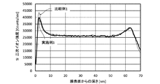
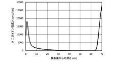
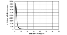
- the depth direction (film thickness direction) by secondary ion mass spectrometry (SIMS) for one phase shift film 2 of the substrate with the thin film of Example 1 and one substrate with the thin film of Comparative Example 1 was analyzed.
- a quadrupole type secondary ion mass spectrometer (PHI ADEPT1010, manufactured by ULVAC-PHI) is used as an analyzer, the primary ion species is Cs + , the primary acceleration voltage is 2.0 kV, and the primary ion irradiation.
- region was performed on the analysis conditions of the square inside area
- Example 1 is represented by a thin line.
- FIG. 4 Example 1 is represented by a thick line, and Comparative Example 1 is represented by a thin line). It is shown in
- the secondary ion intensity of silicon is clear in the region (surface layer region) from the surface of the phase shift film 2 to a depth of 10 nm. It can be seen that the largest peak is detected. However, the maximum peak Si_max of the secondary ion intensity of silicon in the phase shift film 2 of Example 1 is clearly smaller than the maximum peak Si_max of the secondary ion intensity of silicon in the phase shift film 2 of Comparative Example 1. Show. In the phase shift film 2, the distribution in the depth direction of the secondary ion intensity of silicon in the region (near region) extending from the interface of the translucent substrate 1 to the surface layer region up to 20 nm is the phase shift film of Example 1.
- the ratio (percentage; hereinafter referred to as “Mo / [Mo + Si] ratio”) obtained by dividing the molybdenum content [atomic%] in the phase shift film 2 by the total content [atomic%] of molybdenum and silicon. was 11.2%.
- a translucent substrate 1 on which a phase shift film 2 is formed is installed in a single-wafer DC sputtering apparatus, and a chromium (Cr) target is used, and argon (Ar), carbon dioxide (CO 2 ), and nitrogen (N 2 ).
- Ar argon
- N 2 nitrogen
- the lower layer of the light shielding film 3 made of CrN was formed to a thickness of 4 nm on the lowermost layer of the light shielding film 3 by reactive sputtering (DC sputtering).
- the upper layer of 3 was formed with a thickness of 14 nm.
- the light-shielding film 3 made of a chromium-based material having a three-layer structure of the lowermost layer made of CrOCN, the lower layer made of CrN, and the upper layer made of CrOCN was formed with a total film thickness of 48 nm from the phase shift film 2 side.
- the optical density (OD) with respect to the light of wavelength 193nm in the laminated structure of this phase shift film 2 and the light shielding film 3 was measured, it was 3.0 or more.
- the translucent substrate 1 in which the phase shift film 2 and the light-shielding film 3 are laminated in this order is installed in a single wafer RF sputtering apparatus, and a silicon dioxide (SiO 2 ) target is used, and argon (Ar) gas is used.
- a hard mask film 4 made of silicon and oxygen was formed to a thickness of 5 nm on the light shielding film 3 by RF sputtering using a sputtering gas.
- phase shift mask 200 of Example 1 and the phase shift mask of Comparative Example 1 were manufactured in the following procedure.
- the surface of the hard mask film 4 was subjected to HMDS treatment.
- a resist film made of a chemically amplified resist for electron beam drawing with a film thickness of 80 nm was formed in contact with the surface of the hard mask film 4 by spin coating.
- a first pattern which is a phase shift pattern to be formed on the phase shift film 2 is drawn on the resist film with an electron beam, a predetermined development process and a cleaning process are performed, and a first pattern having the first pattern 1 resist pattern 5a was formed (see FIG. 2A).
- the first pattern (light shielding pattern 3a) was formed on the light shielding film 3 (see FIG. 2C).
- dry etching using fluorine-based gas (SF 6 + He) is performed to form a first pattern (phase shift pattern 2a) on the phase shift film 2, and at the same time, a hard mask pattern 4a was removed (see FIG. 2 (d)).
- a resist film made of a chemically amplified resist for electron beam lithography was formed on the light-shielding pattern 3a with a film thickness of 150 nm by spin coating.
- a second pattern which is a pattern to be formed on the light shielding film (light shielding band pattern)
- a predetermined process such as a development process is further performed, so that the second pattern having the light shielding pattern A resist pattern 6b was formed (see FIG. 2E).
- dry etching high bias etching with a bias voltage of 50 [W]
- the second pattern (light-shielding pattern 3b) was formed on the light-shielding film 3 (see FIG. 2F). Further, the second resist pattern 6b was removed, and through a predetermined process such as cleaning, the phase shift mask 200 of Example 1 and the phase shift mask of Comparative Example 1 were obtained (see FIG. 2G).
- each of the manufactured phase shift mask 200 of Example 1 and the phase shift mask of Comparative Example 1 was washed with an alkaline solution (washing of the phase shift mask) under the same conditions.
- the solution of was used.
- the cleaning time in the cleaning process was 60 minutes.
- each phase shift mask 200 after the cleaning step with an alkaline solution was rinsed with DIW (DeIonized Warer).
- the film loss amount of the phase shift mask 200 of Example 1 could be reduced to 1 ⁇ 2 or less of the film loss amount of the phase shift mask of Comparative Example 1 regardless of the same cleaning conditions. That is, it can be said that the phase shift mask 200 of Example 1 has a reduced amount of film loss due to mask cleaning and improved chemical resistance.
- phase shift mask of Comparative Example 1 after performing the above-described cleaning process, similarly to Example 1, AIMS 193 (manufactured by Carl Zeiss) was used to expose the semiconductor device with exposure light having a wavelength of 193 nm. The transfer image was simulated when exposed and transferred to the resist film. When the exposure transfer image of this simulation was verified, a transfer failure was confirmed. This is presumed to be due to the fact that the amount of film loss of the phase shift pattern 2a is large. From this result, when the phase shift mask of Comparative Example 1 is set on the mask stage of the exposure apparatus and exposed and transferred to the resist film on the semiconductor device, there is a defective portion in the circuit pattern finally formed on the semiconductor device. It can be said that it will occur.
- AIMS 193 manufactured by Carl Zeiss
- Comparative Example 2 Comparative Example 3
- the mask blanks of Comparative Example 2 and Comparative Example 3 were manufactured in the same procedure as the mask blanks of Example 1 and Comparative Example 1 except for the phase shift film 2.
- the phase shift film 2 of Comparative Example 1 is significantly different from the phase shift film 2 of Example 1 and Comparative Example 1 in that the Mo / [Mo + Si] ratio of the target is changed.
- the phase shift film 2 made of molybdenum, silicon, and nitrogen oxygen is made 93 nm by reactive sputtering (DC sputtering) using a mixed gas of argon (Ar), nitrogen (N 2 ), and helium (He) as a sputtering gas. Formed in thickness.
- Two of the light-transmitting substrates 1 (hereinafter referred to as thin film-attached substrates) provided with the four phase shift films 2 are used for manufacturing the mask blank of Comparative Example 2, and the remaining two are used for Comparative Example 3. Used for manufacturing mask blanks.
- Example 2 the first heat treatment step similar to that in Example 1 was performed on each of the two substrates with thin films of Comparative Example 2 using hot plates. Then, the 2nd heating similar to Example 1 and the comparative example 1 is performed with respect to the two board
- phase shift film 2 having a wavelength of 248 nm is used.
- MCM248 manufactured by Lasertec Corporation
- the transmittance and phase difference for light were measured, the transmittance was 5.5% and the phase difference was 177.0 degrees (deg). There was no substantial difference in optical characteristics between the phase shift film 2 of Comparative Example 2 and the phase shift film 2 of Comparative Example 3.
- Example 2 was applied to the phase shift film 2 of one thin film-coated substrate of Comparative Example 2 and one thin film-coated substrate of Comparative Example 3.
- Analysis in the depth direction was performed.
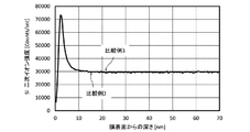
- the results of depth direction analysis of the secondary ion intensity of silicon (Si) in each phase shift film 2 of Example 1 and Comparative Example 1 are shown in FIG. 5 (Example 2 is represented by a thick line and Comparative Example 3 is represented by a thin line). Show.
- a light-shielding film 3 was formed on the remaining thin film-attached substrates of Comparative Example 2 and Comparative Example 3 that were not analyzed in the depth direction by SIMS.
- the light shielding film 3 is the same as the light shielding film 3 of Example 1 except that the thickness of the lower layer (CrN) is changed to 14 nm (that is, the thickness of the light shielding film 3 is 58 nm).
- the optical density (OD) with respect to the light of wavelength 248nm in the laminated structure of this phase shift film 2 and the light shielding film 3 was measured, it was 3.0 or more.
- a hard mask film 4 was formed on the light shielding film 3 under the same conditions as in Example 1.
- phase shift masks of Comparative Example 2 and Comparative Example 3 were produced in the same procedure as in Example 1.
- Translucent substrate Phase shift film (thin film for pattern formation) 2a phase shift pattern 3 light shielding films 3a and 3b light shielding pattern 4 hard mask film 4a hard mask pattern 5a first resist pattern 6b second resist pattern 100 mask blank 200 phase shift mask
Landscapes
- Physics & Mathematics (AREA)
- General Physics & Mathematics (AREA)
- Engineering & Computer Science (AREA)
- Health & Medical Sciences (AREA)
- Life Sciences & Earth Sciences (AREA)
- Toxicology (AREA)
- Atmospheric Sciences (AREA)
- Environmental & Geological Engineering (AREA)
- Epidemiology (AREA)
- Public Health (AREA)
- Optics & Photonics (AREA)
- Plasma & Fusion (AREA)
- Preparing Plates And Mask In Photomechanical Process (AREA)
- Exposure And Positioning Against Photoresist Photosensitive Materials (AREA)
- Physical Vapour Deposition (AREA)
Abstract
Description
(構成1)
透光性基板上にパターン形成用の薄膜を備えたマスクブランクであって、
前記薄膜は、金属、ケイ素および窒素を含有する材料からなり、
前記薄膜における前記金属の含有量[原子%]を前記金属およびケイ素の合計含有量[原子%]で除した比率は、15%以下であり、
前記薄膜に対し、二次イオン質量分析法による分析を行ってケイ素の二次イオン強度の深さ方向の分布を取得したとき、前記薄膜の透光性基板とは反対側の表層領域における前記ケイ素の二次イオン強度の最大ピーク[Counts/sec]を、前記薄膜における前記透光性基板の界面との近傍領域と前記表層領域を除いた領域である内部領域の深さ方向における前記ケイ素の二次イオン強度の平均値[Counts/sec]で除した比率が1.6以下である
ことを特徴とするマスクブランク。
前記表層領域は、前記薄膜における前記透光性基板とは反対側の表面から前記透光性基板側に向かって10nmの深さまでの範囲にわたる領域であることを特徴とする構成1記載のマスクブランク。
前記近傍領域は、前記透光性基板との界面から前記表層領域側に向かって20nmの深さまでの範囲にわたる領域であることを特徴とする構成1または2に記載のマスクブランク。
前記ケイ素の二次イオン強度の深さ方向の分布は、一次イオン種がCs+、一次加速電圧が2.0kV、一次イオンの照射領域を一辺が120μmである四角形の内側領域とした測定条件で取得されるものであることを特徴とする構成1から3のいずれかに記載のマスクブランク。
前記薄膜に対し、二次イオン質量分析法による分析を行って酸素の二次イオン強度の深さ方向の分布も取得したとき、前記内部領域の深さ方向における前記酸素の二次イオン強度の平均値が2000[Counts/sec]以下であることを特徴とする構成1から4のいずれかに記載のマスクブランク。
前記薄膜は、ArFエキシマレーザーの露光光を1%以上の透過率で透過させる機能と、前記薄膜を透過した前記露光光に対して前記薄膜の厚さと同じ距離だけ空気中を通過した前記露光光との間で150度以上190度以下の位相差を生じさせる機能とを有する位相シフト膜であることを特徴とする構成1から5のいずれかに記載のマスクブランク。
前記位相シフト膜上に、遮光膜を備えることを特徴とする構成6記載のマスクブランク。
前記遮光膜は、クロムを含有する材料からなることを特徴とする構成7記載のマスクブランク。
透光性基板上にパターン形成用の薄膜を備えたマスクブランクの製造方法であって、
前記透光性基板上に、金属、ケイ素および窒素を含有する材料であり、前記金属の含有量[原子%]を前記金属およびケイ素の合計含有量[原子%]で除した比率が15%以下である材料からなる前記薄膜を形成する工程と、
前記薄膜に対し、酸素を含む気体中で300℃未満の温度で加熱処理を行う第1加熱処理工程と、
前記第1加熱処理工程後の前記薄膜に対し、酸素を含む気体中で300℃以上の温度で加熱処理を行う第2加熱処理工程と
を有することを特徴とするマスクブランクの製造方法。
前記薄膜は、二次イオン質量分析法による分析を行ってケイ素の二次イオン強度の前記薄膜における深さ方向の分布を取得したとき、前記薄膜の透光性基板とは反対側の表層領域における前記ケイ素の二次イオン強度の最大ピーク[Counts/sec]を、前記薄膜における前記透光性基板の界面との近傍領域と前記表層領域を除いた領域である内部領域の深さ方向における前記ケイ素の二次イオン強度の平均値[Counts/sec]で除した比率が1.6以下であることを特徴とする構成9記載のマスクブランクの製造方法。
前記表層領域は、前記薄膜における前記透光性基板とは反対側の表面から前記透光性基板側に向かって10nmの深さまでの範囲にわたる領域であることを特徴とする構成10記載のマスクブランクの製造方法。
前記近傍領域は、前記透光性基板との界面から前記表層領域側に向かって20nmの深さまでの範囲にわたる領域であることを特徴とする構成10または11に記載のマスクブランクの製造方法。
前記ケイ素の二次イオン強度の深さ方向の分布は、一次イオン種がCs+、一次加速電圧が2.0kV、一次イオンの照射領域を一辺が120μmである四角形の内側領域とした測定条件で取得されるものであることを特徴とする構成10から12のいずれかに記載のマスクブランクの製造方法。
前記薄膜に対し、二次イオン質量分析法による分析を行って酸素の二次イオン強度の深さ方向の分布も取得したとき、前記内部領域の深さ方向における前記酸素の二次イオン強度の平均値が2000[Counts/sec]以下であることを特徴とする構成10から13のいずれかに記載のマスクブランクの製造方法。
前記薄膜は、ArFエキシマレーザーの露光光を1%以上の透過率で透過させる機能と、前記薄膜を透過した前記露光光に対して前記薄膜の厚さと同じ距離だけ空気中を通過した前記露光光との間で150度以上190度以下の位相差を生じさせる機能とを有する位相シフト膜であることを特徴とする構成9から14のいずれかに記載のマスクブランクの製造方法。
前記第2加熱処理工程を行った後の位相シフト膜である薄膜上に、遮光膜を形成する工程を有することを特徴とする構成15記載のマスクブランクの製造方法。
前記遮光膜は、クロムを含有する材料により形成されることを特徴とする構成16記載のマスクブランクの製造方法。
構成1から8のいずれかに記載のマスクブランクの前記薄膜にドライエッチングで転写パターンを形成する工程を有することを特徴とする転写用マスクの製造方法。
構成9から17のいずれかに記載のマスクブランクの製造方法により製造したマスクブランクの前記薄膜にドライエッチングで転写パターンを形成する工程を有することを特徴とする転写用マスクの製造方法。
構成18または19に記載の転写用マスクの製造方法により製造された転写用マスクを用い、半導体基板上のレジスト膜に転写パターンを露光転写する工程を有することを特徴とする半導体デバイスの製造方法。
本発明者らは、金属、ケイ素および窒素を含有する材料からなるパターン形成用の薄膜において、高い耐薬性を有し、かつ塩素系ガスと酸素ガスの混合ガスによるドライエッチングに対する高い耐性を有するような構成について、鋭意研究を行った。薄膜全体を結晶質とすることや薄膜の表層を結晶質の層(二酸化ケイ素の結晶構造の層)とすることで、薄膜の耐薬性やドライエッチング耐性を高めることは可能である。しかし、薄膜に結晶質の層が存在すると、その薄膜にパターンを形成したときのパターン側壁のラインエッジラフネス(LER)が悪く、微細パターンを備える転写用マスクに求められる条件を満たすことができない。パターン形成用薄膜は、アモルファス構造あるいは微結晶構造とする必要がある。
図1は、本発明の実施形態に係る位相シフトマスクを製造するためのマスクブランク100の構成を示す断面図である。図1に示すマスクブランク100は、位相シフトマスクを製造するためのものであり、透光性基板1上に、位相シフト膜(パターン形成用の薄膜)2、遮光膜3およびハードマスク膜4がこの順に積層された構造を有する。
(実施例1および比較例1)
[マスクブランクの製造]
主表面の寸法が約152mm×約152mmで、厚さが約6.35mmの合成石英ガラスからなる透光性基板1を4枚準備した。この透光性基板1は、端面及び主表面を所定の表面粗さに研磨され、その後、所定の洗浄処理および乾燥処理を施されたものであった。
次に、この実施例1のマスクブランク100と比較例1のマスクブランクを用い、以下の手順で実施例1の位相シフトマスク200と比較例1の位相シフトマスクをそれぞれ製造した。最初に、ハードマスク膜4の表面にHMDS処理を施した。続いて、スピン塗布法によって、ハードマスク膜4の表面に接して、電子線描画用化学増幅型レジストからなるレジスト膜を膜厚80nmで形成した。次に、このレジスト膜に対して、位相シフト膜2に形成すべき位相シフトパターンである第1のパターンを電子線描画し、所定の現像処理および洗浄処理を行い、第1のパターンを有する第1のレジストパターン5aを形成した(図2(a)参照)。
上記の洗浄工程を行った後の実施例1の位相シフトマスク200に対し、AIMS193(Carl Zeiss社製)を用いて、波長193nmの露光光で半導体デバイス上のレジスト膜に露光転写したときにおける転写像のシミュレーションを行った。このシミュレーションの露光転写像を検証したところ、設計仕様を十分に満たしていた。この結果から、上記の洗浄工程を行った後の実施例1の位相シフトマスク200を露光装置のマスクステージにセットし、半導体デバイス上のレジスト膜に露光転写したとしても、最終的に半導体デバイス上に形成される回路パターンは高精度で形成できるといえる。
[マスクブランクの製造]
この比較例2および比較例3のマスクブランクは、位相シフト膜2以外については、実施例1および比較例1のマスクブランクと同様の手順で製造した。この比較例1の位相シフト膜2は、ターゲットのMo/[Mo+Si]比率を変えた点が実施例1および比較例1の位相シフト膜2とは大きく異なる。具体的には、枚葉式DCスパッタ装置内に透光性基板1を設置し、モリブデン(Mo)とケイ素(Si)との混合焼結ターゲット(Mo:Si=21原子%:79原子%)を用い、アルゴン(Ar)、窒素(N2)およびヘリウム(He)の混合ガスをスパッタリングガスとする反応性スパッタリング(DCスパッタリング)により、モリブデン、ケイ素および窒素酸素からなる位相シフト膜2を93nmの厚さで形成した。この4枚の位相シフト膜2を備える透光性基板1(以下、薄膜付き基板という。)の内、2枚を比較例2のマスクブランクの製造に用い、残りの2枚を比較例3のマスクブランクの製造に用いる。
次に、この比較例2および比較例3のマスクブランクを用い、実施例1と同様の手順で、比較例2および比較例3の位相シフトマスクを作製した。
上記の洗浄工程を行った後の比較例2および比較例3の各位相シフトマスクに対し、AIMS248(Carl Zeiss社製)を用いて、波長248nmの露光光で半導体デバイス上のレジスト膜に露光転写したときにおける転写像のシミュレーションを行った。このシミュレーションの露光転写像を検証したところ、転写不良が確認された。これは、位相シフトパターン2aの膜減り量が大きいことが転写不良の発生要因と推察される。この結果から、この比較例2および比較例3の位相シフトマスクを露光装置のマスクステージにセットし、半導体デバイス上のレジスト膜に露光転写した場合、最終的に半導体デバイス上に形成される回路パターンに不良箇所が発生してしまうといえる。
2 位相シフト膜(パターン形成用の薄膜)
2a 位相シフトパターン
3 遮光膜
3a,3b 遮光パターン
4 ハードマスク膜
4a ハードマスクパターン
5a 第1のレジストパターン
6b 第2のレジストパターン
100 マスクブランク
200 位相シフトマスク
Claims (20)
- 透光性基板上にパターン形成用の薄膜を備えたマスクブランクであって、
前記薄膜は、金属、ケイ素および窒素を含有する材料からなり、
前記薄膜における前記金属の含有量[原子%]を前記金属およびケイ素の合計含有量[原子%]で除した比率は、15%以下であり、
前記薄膜に対し、二次イオン質量分析法による分析を行ってケイ素の二次イオン強度の深さ方向の分布を取得したとき、前記薄膜の透光性基板とは反対側の表層領域における前記ケイ素の二次イオン強度の最大ピーク[Counts/sec]を、前記薄膜における前記透光性基板の界面との近傍領域と前記表層領域を除いた領域である内部領域の深さ方向における前記ケイ素の二次イオン強度の平均値[Counts/sec]で除した比率が1.6以下である
ことを特徴とするマスクブランク。 - 前記表層領域は、前記薄膜における前記透光性基板とは反対側の表面から前記透光性基板側に向かって10nmの深さまでの範囲にわたる領域であることを特徴とする請求項1記載のマスクブランク。
- 前記近傍領域は、前記透光性基板との界面から前記表層領域側に向かって20nmの深さまでの範囲にわたる領域であることを特徴とする請求項1または2に記載のマスクブランク。
- 前記ケイ素の二次イオン強度の深さ方向の分布は、一次イオン種がCs+、一次加速電圧が2.0kV、一次イオンの照射領域を一辺が120μmである四角形の内側領域とした測定条件で取得されるものであることを特徴とする請求項1から3のいずれかに記載のマスクブランク。
- 前記薄膜に対し、二次イオン質量分析法による分析を行って酸素の二次イオン強度の深さ方向の分布を取得したとき、前記内部領域の深さ方向における前記酸素の二次イオン強度の平均値が2000[Counts/sec]以下であることを特徴とする請求項1から4のいずれかに記載のマスクブランク。
- 前記薄膜は、ArFエキシマレーザーの露光光を1%以上の透過率で透過させる機能と、前記薄膜を透過した前記露光光に対して前記薄膜の厚さと同じ距離だけ空気中を通過した前記露光光との間で150度以上190度以下の位相差を生じさせる機能とを有する位相シフト膜であることを特徴とする請求項1から5のいずれかに記載のマスクブランク。
- 前記位相シフト膜上に、遮光膜を備えることを特徴とする請求項6記載のマスクブランク。
- 前記遮光膜は、クロムを含有する材料からなることを特徴とする請求項7記載のマスクブランク。
- 透光性基板上にパターン形成用の薄膜を備えたマスクブランクの製造方法であって、
前記透光性基板上に、金属、ケイ素および窒素を含有する材料であり、前記金属の含有量[原子%]を前記金属およびケイ素の合計含有量[原子%]で除した比率が15%以下である材料からなる前記薄膜を形成する工程と、
前記薄膜に対し、酸素を含む気体中で300℃未満の温度で加熱処理を行う第1加熱処理工程と、
前記第1加熱処理工程後の前記薄膜に対し、酸素を含む気体中で300℃以上の温度で加熱処理を行う第2加熱処理工程と
を有することを特徴とするマスクブランクの製造方法。 - 前記薄膜は、二次イオン質量分析法による分析を行ってケイ素の二次イオン強度の前記薄膜における深さ方向の分布を取得したとき、前記薄膜の透光性基板とは反対側の表層領域における前記ケイ素の二次イオン強度の最大ピーク[Counts/sec]を、前記薄膜における前記透光性基板の界面との近傍領域と前記表層領域を除いた領域である内部領域の深さ方向における前記ケイ素の二次イオン強度の平均値[Counts/sec]で除した比率が1.6以下であることを特徴とする請求項9記載のマスクブランクの製造方法。
- 前記表層領域は、前記薄膜における前記透光性基板とは反対側の表面から前記透光性基板側に向かって10nmの深さまでの範囲にわたる領域であることを特徴とする請求項10記載のマスクブランクの製造方法。
- 前記近傍領域は、前記透光性基板との界面から前記表層領域側に向かって20nmの深さまでの範囲にわたる領域であることを特徴とする請求項10または11に記載のマスクブランクの製造方法。
- 前記ケイ素の二次イオン強度の深さ方向の分布は、一次イオン種がCs+、一次加速電圧が2.0kV、一次イオンの照射領域を一辺が120μmである四角形の内側領域とした測定条件で取得されるものであることを特徴とする請求項10から12のいずれかに記載のマスクブランクの製造方法。
- 前記薄膜に対し、二次イオン質量分析法による分析を行って酸素の二次イオン強度の深さ方向の分布も取得したとき、前記内部領域の深さ方向における前記酸素の二次イオン強度の平均値が2000[Counts/sec]以下であることを特徴とする請求項10から13のいずれかに記載のマスクブランクの製造方法。
- 前記薄膜は、ArFエキシマレーザーの露光光を1%以上の透過率で透過させる機能と、前記薄膜を透過した前記露光光に対して前記薄膜の厚さと同じ距離だけ空気中を通過した前記露光光との間で150度以上190度以下の位相差を生じさせる機能とを有する位相シフト膜であることを特徴とする請求項9から14のいずれかに記載のマスクブランクの製造方法。
- 前記第2加熱処理工程を行った後の位相シフト膜である薄膜上に、遮光膜を形成する工程を有することを特徴とする請求項15記載のマスクブランクの製造方法。
- 前記遮光膜は、クロムを含有する材料により形成されることを特徴とする請求項16記載のマスクブランクの製造方法。
- 請求項1から8のいずれかに記載のマスクブランクの前記薄膜にドライエッチングで転写パターンを形成する工程を有することを特徴とする転写用マスクの製造方法。
- 請求項9から17のいずれかに記載のマスクブランクの製造方法により製造したマスクブランクの前記薄膜にドライエッチングで転写パターンを形成する工程を有することを特徴とする転写用マスクの製造方法。
- 請求項18または19に記載の転写用マスクの製造方法により製造された転写用マスクを用い、半導体基板上のレジスト膜に転写パターンを露光転写する工程を有することを特徴とする半導体デバイスの製造方法。
Priority Applications (4)
| Application Number | Priority Date | Filing Date | Title |
|---|---|---|---|
| JP2017547187A JP6495472B2 (ja) | 2016-03-29 | 2017-03-08 | マスクブランク、マスクブランクの製造方法、転写用マスクの製造方法および半導体デバイスの製造方法 |
| SG11201807932XA SG11201807932XA (en) | 2016-03-29 | 2017-03-08 | Mask blank, method for manufacturing mask blank, method for manufacturing transfer mask, and method for manufacturing semiconductor device |
| KR1020187026745A KR102313892B1 (ko) | 2016-03-29 | 2017-03-08 | 마스크 블랭크, 마스크 블랭크의 제조 방법, 전사용 마스크의 제조 방법 및 반도체 디바이스의 제조 방법 |
| US16/085,316 US11327396B2 (en) | 2016-03-29 | 2017-03-08 | Mask blank |
Applications Claiming Priority (2)
| Application Number | Priority Date | Filing Date | Title |
|---|---|---|---|
| JP2016065394 | 2016-03-29 | ||
| JP2016-065394 | 2016-03-29 |
Publications (1)
| Publication Number | Publication Date |
|---|---|
| WO2017169587A1 true WO2017169587A1 (ja) | 2017-10-05 |
Family
ID=59963104
Family Applications (1)
| Application Number | Title | Priority Date | Filing Date |
|---|---|---|---|
| PCT/JP2017/009201 Ceased WO2017169587A1 (ja) | 2016-03-29 | 2017-03-08 | マスクブランク、マスクブランクの製造方法、転写用マスクの製造方法および半導体デバイスの製造方法 |
Country Status (6)
| Country | Link |
|---|---|
| US (1) | US11327396B2 (ja) |
| JP (2) | JP6495472B2 (ja) |
| KR (1) | KR102313892B1 (ja) |
| SG (1) | SG11201807932XA (ja) |
| TW (2) | TWI702466B (ja) |
| WO (1) | WO2017169587A1 (ja) |
Cited By (3)
| Publication number | Priority date | Publication date | Assignee | Title |
|---|---|---|---|---|
| WO2019058984A1 (ja) * | 2017-09-21 | 2019-03-28 | Hoya株式会社 | マスクブランク、転写用マスク、及び半導体デバイスの製造方法 |
| JP2019191603A (ja) * | 2019-06-24 | 2019-10-31 | Hoya株式会社 | マスクブランク、位相シフトマスク及び半導体デバイスの製造方法 |
| JP2022118976A (ja) * | 2021-02-03 | 2022-08-16 | アルバック成膜株式会社 | マスクブランクス及びフォトマスク |
Families Citing this family (3)
| Publication number | Priority date | Publication date | Assignee | Title |
|---|---|---|---|---|
| JP7329033B2 (ja) | 2020-12-31 | 2023-08-17 | エスケー エンパルス カンパニー リミテッド | ブランクマスク及びそれを用いたフォトマスク |
| JP7329031B2 (ja) * | 2020-12-31 | 2023-08-17 | エスケー エンパルス カンパニー リミテッド | ブランクマスク及びそれを用いたフォトマスク |
| KR102444967B1 (ko) | 2021-04-29 | 2022-09-16 | 에스케이씨솔믹스 주식회사 | 블랭크 마스크 및 이를 이용한 포토마스크 |
Citations (7)
| Publication number | Priority date | Publication date | Assignee | Title |
|---|---|---|---|---|
| JP2010039300A (ja) * | 2008-08-06 | 2010-02-18 | Dainippon Printing Co Ltd | ハーフトーン型位相シフトマスクの製造方法 |
| JP2011112824A (ja) * | 2009-11-26 | 2011-06-09 | Hoya Corp | マスクブランク及び転写用マスク並びにそれらの製造方法 |
| JP2012003255A (ja) * | 2010-05-19 | 2012-01-05 | Hoya Corp | マスクブランクの製造方法及び転写用マスクの製造方法、並びにマスクブランク及び転写用マスク |
| JP2013088814A (ja) * | 2011-10-17 | 2013-05-13 | S&S Tech Corp | ブランクマスク及びこれを用いたフォトマスク |
| JP2015121801A (ja) * | 2012-07-13 | 2015-07-02 | Hoya株式会社 | マスクブランク及び位相シフトマスクの製造方法 |
| WO2015141078A1 (ja) * | 2014-03-18 | 2015-09-24 | Hoya株式会社 | マスクブランク、位相シフトマスクおよび半導体デバイスの製造方法 |
| JP2016004223A (ja) * | 2014-06-19 | 2016-01-12 | Hoya株式会社 | マスクブランク、位相シフトマスク、位相シフトマスクの製造方法および半導体デバイスの製造方法 |
Family Cites Families (16)
| Publication number | Priority date | Publication date | Assignee | Title |
|---|---|---|---|---|
| JP3722029B2 (ja) | 2000-09-12 | 2005-11-30 | Hoya株式会社 | 位相シフトマスクブランクの製造方法、及び位相シフトマスクの製造方法 |
| JP2002090978A (ja) | 2000-09-12 | 2002-03-27 | Hoya Corp | 位相シフトマスクブランクの製造方法、及び位相シフトマスクブランクの製造装置 |
| WO2005024518A2 (en) * | 2003-09-05 | 2005-03-17 | Schott Ag | Phase shift mask blank with increased uniformity |
| US7029803B2 (en) | 2003-09-05 | 2006-04-18 | Schott Ag | Attenuating phase shift mask blank and photomask |
| JP4407815B2 (ja) * | 2004-09-10 | 2010-02-03 | 信越化学工業株式会社 | フォトマスクブランク及びフォトマスク |
| KR100617389B1 (ko) * | 2005-05-16 | 2006-08-31 | 주식회사 피케이엘 | 헤이즈 방지를 위한 위상편이 마스크 |
| KR20070096749A (ko) * | 2006-06-20 | 2007-10-02 | 주식회사 에스앤에스텍 | 블랭크 마스크 및 그 제조방법 |
| JP4489820B2 (ja) * | 2008-03-31 | 2010-06-23 | Hoya株式会社 | 位相シフトマスクブランクの製造方法、及び位相シフトマスクブランクの製造装置 |
| JP5497288B2 (ja) | 2008-12-29 | 2014-05-21 | Hoya株式会社 | フォトマスクブランクの製造方法及びフォトマスクの製造方法 |
| JP5221495B2 (ja) | 2009-11-30 | 2013-06-26 | Hoya株式会社 | マスクブランクの製造方法 |
| MX344792B (es) * | 2011-09-25 | 2017-01-06 | Theranos Inc | Sistemas y métodos para múltiples análisis. |
| US20150079502A1 (en) | 2012-03-14 | 2015-03-19 | Hoya Corporation | Mask blank and method of manufacturing a transfer mask |
| KR101862166B1 (ko) * | 2012-03-14 | 2018-05-29 | 호야 가부시키가이샤 | 마스크 블랭크, 및 전사용 마스크의 제조방법 |
| SG11201505421SA (en) | 2013-01-18 | 2015-08-28 | Hoya Corp | Method for manufacturing mask blank substrate, method for manufacturing mask blank and method for manufacturing transfer mask |
| JP6150299B2 (ja) | 2014-03-30 | 2017-06-21 | Hoya株式会社 | マスクブランク、転写用マスクの製造方法及び半導体装置の製造方法 |
| JP6087401B2 (ja) * | 2015-08-14 | 2017-03-01 | Hoya株式会社 | マスクブランク、位相シフトマスクおよび半導体デバイスの製造方法 |
-
2017
- 2017-03-08 KR KR1020187026745A patent/KR102313892B1/ko active Active
- 2017-03-08 WO PCT/JP2017/009201 patent/WO2017169587A1/ja not_active Ceased
- 2017-03-08 SG SG11201807932XA patent/SG11201807932XA/en unknown
- 2017-03-08 US US16/085,316 patent/US11327396B2/en active Active
- 2017-03-08 JP JP2017547187A patent/JP6495472B2/ja active Active
- 2017-03-21 TW TW106109376A patent/TWI702466B/zh active
- 2017-03-21 TW TW109124427A patent/TWI741687B/zh active
-
2019
- 2019-03-01 JP JP2019037453A patent/JP6786645B2/ja active Active
Patent Citations (8)
| Publication number | Priority date | Publication date | Assignee | Title |
|---|---|---|---|---|
| JP2010039300A (ja) * | 2008-08-06 | 2010-02-18 | Dainippon Printing Co Ltd | ハーフトーン型位相シフトマスクの製造方法 |
| JP2011112824A (ja) * | 2009-11-26 | 2011-06-09 | Hoya Corp | マスクブランク及び転写用マスク並びにそれらの製造方法 |
| JP2012003255A (ja) * | 2010-05-19 | 2012-01-05 | Hoya Corp | マスクブランクの製造方法及び転写用マスクの製造方法、並びにマスクブランク及び転写用マスク |
| JP2013088814A (ja) * | 2011-10-17 | 2013-05-13 | S&S Tech Corp | ブランクマスク及びこれを用いたフォトマスク |
| JP2015121801A (ja) * | 2012-07-13 | 2015-07-02 | Hoya株式会社 | マスクブランク及び位相シフトマスクの製造方法 |
| WO2015141078A1 (ja) * | 2014-03-18 | 2015-09-24 | Hoya株式会社 | マスクブランク、位相シフトマスクおよび半導体デバイスの製造方法 |
| JP2016021075A (ja) * | 2014-03-18 | 2016-02-04 | Hoya株式会社 | マスクブランク、位相シフトマスクおよび半導体デバイスの製造方法 |
| JP2016004223A (ja) * | 2014-06-19 | 2016-01-12 | Hoya株式会社 | マスクブランク、位相シフトマスク、位相シフトマスクの製造方法および半導体デバイスの製造方法 |
Cited By (4)
| Publication number | Priority date | Publication date | Assignee | Title |
|---|---|---|---|---|
| WO2019058984A1 (ja) * | 2017-09-21 | 2019-03-28 | Hoya株式会社 | マスクブランク、転写用マスク、及び半導体デバイスの製造方法 |
| JP2019056910A (ja) * | 2017-09-21 | 2019-04-11 | Hoya株式会社 | マスクブランク、転写用マスク、及び半導体デバイスの製造方法 |
| JP2019191603A (ja) * | 2019-06-24 | 2019-10-31 | Hoya株式会社 | マスクブランク、位相シフトマスク及び半導体デバイスの製造方法 |
| JP2022118976A (ja) * | 2021-02-03 | 2022-08-16 | アルバック成膜株式会社 | マスクブランクス及びフォトマスク |
Also Published As
| Publication number | Publication date |
|---|---|
| TWI702466B (zh) | 2020-08-21 |
| JP2019082737A (ja) | 2019-05-30 |
| KR20180128403A (ko) | 2018-12-03 |
| SG11201807932XA (en) | 2018-10-30 |
| US20190064649A1 (en) | 2019-02-28 |
| US11327396B2 (en) | 2022-05-10 |
| JPWO2017169587A1 (ja) | 2018-04-05 |
| KR102313892B1 (ko) | 2021-10-15 |
| TW201800834A (zh) | 2018-01-01 |
| JP6786645B2 (ja) | 2020-11-18 |
| TWI741687B (zh) | 2021-10-01 |
| TW202040261A (zh) | 2020-11-01 |
| JP6495472B2 (ja) | 2019-04-03 |
Similar Documents
| Publication | Publication Date | Title |
|---|---|---|
| US10942441B2 (en) | Mask blank, phase shift mask, and method for manufacturing semiconductor device | |
| US10551734B2 (en) | Mask blank, phase shift mask, method for manufacturing phase shift mask, and method for manufacturing semiconductor device | |
| KR102416957B1 (ko) | 마스크 블랭크, 위상 시프트 마스크의 제조 방법 및 반도체 디바이스의 제조 방법 | |
| JP6786645B2 (ja) | マスクブランク、転写用マスクの製造方法および半導体デバイスの製造方法 | |
| JP6506449B2 (ja) | マスクブランク、位相シフトマスク及び半導体デバイスの製造方法 | |
| JP6430155B2 (ja) | マスクブランク、位相シフトマスク、位相シフトマスクの製造方法および半導体デバイスの製造方法 | |
| US20180259841A1 (en) | Mask blank, transfer mask, method of manufacturing transfer mask and method of manufacturing semiconductor device | |
| JP6552700B2 (ja) | マスクブランク、転写用マスク、及び半導体デバイスの製造方法 | |
| JP2017223890A (ja) | マスクブランク、転写用マスク、マスクブランクの製造方法、転写用マスクの製造方法および半導体デバイスの製造方法 | |
| TW201635008A (zh) | 光罩基底、相移光罩、相移光罩之製造方法及半導體裝置之製造方法 | |
| JP2018132686A (ja) | マスクブランク、転写用マスク、転写用マスクの製造方法および半導体デバイスの製造方法 |
Legal Events
| Date | Code | Title | Description |
|---|---|---|---|
| ENP | Entry into the national phase |
Ref document number: 2017547187 Country of ref document: JP Kind code of ref document: A |
|
| ENP | Entry into the national phase |
Ref document number: 20187026745 Country of ref document: KR Kind code of ref document: A |
|
| WWE | Wipo information: entry into national phase |
Ref document number: 11201807932X Country of ref document: SG |
|
| NENP | Non-entry into the national phase |
Ref country code: DE |
|
| 121 | Ep: the epo has been informed by wipo that ep was designated in this application |
Ref document number: 17774132 Country of ref document: EP Kind code of ref document: A1 |
|
| 122 | Ep: pct application non-entry in european phase |
Ref document number: 17774132 Country of ref document: EP Kind code of ref document: A1 |