WO2017163774A1 - 撮像素子および撮像装置 - Google Patents
撮像素子および撮像装置 Download PDFInfo
- Publication number
- WO2017163774A1 WO2017163774A1 PCT/JP2017/007549 JP2017007549W WO2017163774A1 WO 2017163774 A1 WO2017163774 A1 WO 2017163774A1 JP 2017007549 W JP2017007549 W JP 2017007549W WO 2017163774 A1 WO2017163774 A1 WO 2017163774A1
- Authority
- WO
- WIPO (PCT)
- Prior art keywords
- signal
- unit
- substrate
- pixel
- photoelectric conversion
- Prior art date
Links
- 238000003384 imaging method Methods 0.000 title claims abstract description 45
- 239000000758 substrate Substances 0.000 claims abstract description 123
- 238000006243 chemical reaction Methods 0.000 claims abstract description 78
- 238000012937 correction Methods 0.000 claims abstract description 74
- 230000000149 penetrating effect Effects 0.000 claims description 2
- 230000000875 corresponding effect Effects 0.000 description 24
- 238000010586 diagram Methods 0.000 description 11
- 238000009792 diffusion process Methods 0.000 description 11
- 238000012986 modification Methods 0.000 description 9
- 230000004048 modification Effects 0.000 description 9
- 238000012545 processing Methods 0.000 description 8
- 238000012546 transfer Methods 0.000 description 7
- 230000002596 correlated effect Effects 0.000 description 6
- 238000005070 sampling Methods 0.000 description 6
- 238000000034 method Methods 0.000 description 5
- 230000006870 function Effects 0.000 description 4
- 230000003287 optical effect Effects 0.000 description 4
- 238000002161 passivation Methods 0.000 description 3
- 238000009825 accumulation Methods 0.000 description 2
- 230000001276 controlling effect Effects 0.000 description 2
- 230000002093 peripheral effect Effects 0.000 description 2
- 230000003321 amplification Effects 0.000 description 1
- 239000004020 conductor Substances 0.000 description 1
- 230000003247 decreasing effect Effects 0.000 description 1
- 230000000694 effects Effects 0.000 description 1
- 238000005286 illumination Methods 0.000 description 1
- 238000003702 image correction Methods 0.000 description 1
- 230000010354 integration Effects 0.000 description 1
- 239000002184 metal Substances 0.000 description 1
- 150000004767 nitrides Chemical class 0.000 description 1
- 238000003199 nucleic acid amplification method Methods 0.000 description 1
- 239000004065 semiconductor Substances 0.000 description 1
- 230000035945 sensitivity Effects 0.000 description 1
- 229910052710 silicon Inorganic materials 0.000 description 1
- 239000010703 silicon Substances 0.000 description 1
Images


Classifications
-
- H—ELECTRICITY
- H04—ELECTRIC COMMUNICATION TECHNIQUE
- H04N—PICTORIAL COMMUNICATION, e.g. TELEVISION
- H04N25/00—Circuitry of solid-state image sensors [SSIS]; Control thereof
- H04N25/70—SSIS architectures; Circuits associated therewith
- H04N25/79—Arrangements of circuitry being divided between different or multiple substrates, chips or circuit boards, e.g. stacked image sensors
-
- H—ELECTRICITY
- H01—ELECTRIC ELEMENTS
- H01L—SEMICONDUCTOR DEVICES NOT COVERED BY CLASS H10
- H01L27/00—Devices consisting of a plurality of semiconductor or other solid-state components formed in or on a common substrate
- H01L27/14—Devices consisting of a plurality of semiconductor or other solid-state components formed in or on a common substrate including semiconductor components sensitive to infrared radiation, light, electromagnetic radiation of shorter wavelength or corpuscular radiation and specially adapted either for the conversion of the energy of such radiation into electrical energy or for the control of electrical energy by such radiation
- H01L27/144—Devices controlled by radiation
- H01L27/146—Imager structures
- H01L27/14601—Structural or functional details thereof
- H01L27/1464—Back illuminated imager structures
-
- H—ELECTRICITY
- H01—ELECTRIC ELEMENTS
- H01L—SEMICONDUCTOR DEVICES NOT COVERED BY CLASS H10
- H01L27/00—Devices consisting of a plurality of semiconductor or other solid-state components formed in or on a common substrate
- H01L27/14—Devices consisting of a plurality of semiconductor or other solid-state components formed in or on a common substrate including semiconductor components sensitive to infrared radiation, light, electromagnetic radiation of shorter wavelength or corpuscular radiation and specially adapted either for the conversion of the energy of such radiation into electrical energy or for the control of electrical energy by such radiation
- H01L27/144—Devices controlled by radiation
- H01L27/146—Imager structures
- H01L27/14601—Structural or functional details thereof
- H01L27/14603—Special geometry or disposition of pixel-elements, address-lines or gate-electrodes
- H01L27/14605—Structural or functional details relating to the position of the pixel elements, e.g. smaller pixel elements in the center of the imager compared to pixel elements at the periphery
-
- H—ELECTRICITY
- H01—ELECTRIC ELEMENTS
- H01L—SEMICONDUCTOR DEVICES NOT COVERED BY CLASS H10
- H01L27/00—Devices consisting of a plurality of semiconductor or other solid-state components formed in or on a common substrate
- H01L27/14—Devices consisting of a plurality of semiconductor or other solid-state components formed in or on a common substrate including semiconductor components sensitive to infrared radiation, light, electromagnetic radiation of shorter wavelength or corpuscular radiation and specially adapted either for the conversion of the energy of such radiation into electrical energy or for the control of electrical energy by such radiation
- H01L27/144—Devices controlled by radiation
- H01L27/146—Imager structures
- H01L27/14601—Structural or functional details thereof
- H01L27/1462—Coatings
- H01L27/14621—Colour filter arrangements
-
- H—ELECTRICITY
- H01—ELECTRIC ELEMENTS
- H01L—SEMICONDUCTOR DEVICES NOT COVERED BY CLASS H10
- H01L27/00—Devices consisting of a plurality of semiconductor or other solid-state components formed in or on a common substrate
- H01L27/14—Devices consisting of a plurality of semiconductor or other solid-state components formed in or on a common substrate including semiconductor components sensitive to infrared radiation, light, electromagnetic radiation of shorter wavelength or corpuscular radiation and specially adapted either for the conversion of the energy of such radiation into electrical energy or for the control of electrical energy by such radiation
- H01L27/144—Devices controlled by radiation
- H01L27/146—Imager structures
- H01L27/14601—Structural or functional details thereof
- H01L27/14625—Optical elements or arrangements associated with the device
- H01L27/14629—Reflectors
-
- H—ELECTRICITY
- H01—ELECTRIC ELEMENTS
- H01L—SEMICONDUCTOR DEVICES NOT COVERED BY CLASS H10
- H01L27/00—Devices consisting of a plurality of semiconductor or other solid-state components formed in or on a common substrate
- H01L27/14—Devices consisting of a plurality of semiconductor or other solid-state components formed in or on a common substrate including semiconductor components sensitive to infrared radiation, light, electromagnetic radiation of shorter wavelength or corpuscular radiation and specially adapted either for the conversion of the energy of such radiation into electrical energy or for the control of electrical energy by such radiation
- H01L27/144—Devices controlled by radiation
- H01L27/146—Imager structures
- H01L27/14643—Photodiode arrays; MOS imagers
-
- H—ELECTRICITY
- H04—ELECTRIC COMMUNICATION TECHNIQUE
- H04N—PICTORIAL COMMUNICATION, e.g. TELEVISION
- H04N25/00—Circuitry of solid-state image sensors [SSIS]; Control thereof
- H04N25/60—Noise processing, e.g. detecting, correcting, reducing or removing noise
- H04N25/616—Noise processing, e.g. detecting, correcting, reducing or removing noise involving a correlated sampling function, e.g. correlated double sampling [CDS] or triple sampling
-
- H—ELECTRICITY
- H04—ELECTRIC COMMUNICATION TECHNIQUE
- H04N—PICTORIAL COMMUNICATION, e.g. TELEVISION
- H04N25/00—Circuitry of solid-state image sensors [SSIS]; Control thereof
- H04N25/60—Noise processing, e.g. detecting, correcting, reducing or removing noise
- H04N25/63—Noise processing, e.g. detecting, correcting, reducing or removing noise applied to dark current
-
- H—ELECTRICITY
- H04—ELECTRIC COMMUNICATION TECHNIQUE
- H04N—PICTORIAL COMMUNICATION, e.g. TELEVISION
- H04N25/00—Circuitry of solid-state image sensors [SSIS]; Control thereof
- H04N25/70—SSIS architectures; Circuits associated therewith
- H04N25/71—Charge-coupled device [CCD] sensors; Charge-transfer registers specially adapted for CCD sensors
- H04N25/75—Circuitry for providing, modifying or processing image signals from the pixel array
-
- H—ELECTRICITY
- H04—ELECTRIC COMMUNICATION TECHNIQUE
- H04N—PICTORIAL COMMUNICATION, e.g. TELEVISION
- H04N25/00—Circuitry of solid-state image sensors [SSIS]; Control thereof
- H04N25/70—SSIS architectures; Circuits associated therewith
- H04N25/76—Addressed sensors, e.g. MOS or CMOS sensors
- H04N25/77—Pixel circuitry, e.g. memories, A/D converters, pixel amplifiers, shared circuits or shared components
- H04N25/771—Pixel circuitry, e.g. memories, A/D converters, pixel amplifiers, shared circuits or shared components comprising storage means other than floating diffusion
-
- H—ELECTRICITY
- H04—ELECTRIC COMMUNICATION TECHNIQUE
- H04N—PICTORIAL COMMUNICATION, e.g. TELEVISION
- H04N25/00—Circuitry of solid-state image sensors [SSIS]; Control thereof
- H04N25/70—SSIS architectures; Circuits associated therewith
- H04N25/76—Addressed sensors, e.g. MOS or CMOS sensors
- H04N25/77—Pixel circuitry, e.g. memories, A/D converters, pixel amplifiers, shared circuits or shared components
- H04N25/772—Pixel circuitry, e.g. memories, A/D converters, pixel amplifiers, shared circuits or shared components comprising A/D, V/T, V/F, I/T or I/F converters
-
- H—ELECTRICITY
- H01—ELECTRIC ELEMENTS
- H01L—SEMICONDUCTOR DEVICES NOT COVERED BY CLASS H10
- H01L31/00—Semiconductor devices sensitive to infrared radiation, light, electromagnetic radiation of shorter wavelength or corpuscular radiation and specially adapted either for the conversion of the energy of such radiation into electrical energy or for the control of electrical energy by such radiation; Processes or apparatus specially adapted for the manufacture or treatment thereof or of parts thereof; Details thereof
- H01L31/02—Details
- H01L31/02002—Arrangements for conducting electric current to or from the device in operations
- H01L31/02005—Arrangements for conducting electric current to or from the device in operations for device characterised by at least one potential jump barrier or surface barrier
Definitions
- the present invention relates to an imaging element and an imaging apparatus.
- Patent Document 1 An image sensor that calculates signals of adjacent pixels is known (Patent Document 1). Since this image sensor does not perform correlated double sampling (CDS) prior to computation between pixel signals, it cannot remove the noise signal component of each pixel.
- CDS correlated double sampling
- the imaging device includes a plurality of pixels including a photoelectric conversion unit that photoelectrically converts incident light to generate charge and an output unit that generates and outputs a signal based on the charge.
- a correction signal is generated by a reset signal after resetting the charge of the output unit and a photoelectric conversion signal based on the charge generated by the photoelectric conversion unit, and calculation between correction signals generated for each pixel And an arithmetic substrate stacked on the pixel substrate.
- the imaging device includes a pixel substrate on which a plurality of pixels having a photoelectric conversion unit and an output unit are arranged, and a reset signal obtained by digitally converting a signal after resetting the output unit.
- an imaging apparatus includes the imaging element according to the first or second aspect, and an image generation unit that generates image data based on a signal from the pixel.
- FIG. 1 is a block diagram illustrating a configuration of an imaging apparatus according to a first embodiment.
- FIG. 3 is a diagram illustrating a cross-sectional structure of the image sensor according to the first embodiment.
- 1 is a block diagram showing a configuration of an image sensor according to a first embodiment.
- FIG. 3 is a circuit diagram illustrating a configuration of a pixel according to the first embodiment.
- FIG. 3 is a block diagram showing details of the configuration of the image sensor according to the first embodiment.
- 3 is a timing chart showing the operation of the image sensor according to the first embodiment.
- FIG. 9 is a block diagram illustrating details of a configuration of an image sensor according to Modification Example 1.
- FIG. 1 is a block diagram illustrating a configuration of the imaging apparatus according to the first embodiment.
- the imaging device 1 includes an imaging optical system 2, an imaging element 3, and a control unit 4.
- the imaging device 1 is a camera, for example.
- the photographing optical system 2 forms a subject image on the image sensor 3.
- the image sensor 3 captures a subject image formed by the photographing optical system 2 and generates an image signal.
- the image sensor 3 is, for example, a CMOS image sensor.
- the control unit 4 outputs a control signal for controlling the operation of the image sensor 3 to the image sensor 3.
- the control unit 4 functions as an image generation unit that performs various types of image processing on the image signal output from the image sensor 3 and generates image data.
- the photographic optical system 2 may be detachable from the imaging device 1.
- FIG. 2 is a diagram showing a cross-sectional structure of the image sensor according to the first embodiment.
- the imaging element 3 shown in FIG. 2 is a backside illumination type imaging element.
- the image sensor 3 includes a first substrate 111, a second substrate 112, a third substrate 113, and a fourth substrate 114.
- the first substrate 111, the second substrate 112, the third substrate 113, and the fourth substrate 114 are each composed of a semiconductor substrate or the like.
- the first substrate 111 is stacked on the second substrate 112, the second substrate 112 is stacked on the third substrate 113, and the third substrate 113 is stacked on the fourth substrate 114.
- Incident light L indicated by a white arrow enters in the positive direction of the Z axis.
- the left direction of the paper orthogonal to the Z axis is the X axis plus direction
- the front side of the paper orthogonal to the Z axis and the X axis is the Y axis plus direction.
- the imaging device 3 further includes a microlens layer 101, a color filter layer 102, and a passivation layer 103.
- the passivation layer 103, the color filter layer 102, and the microlens layer 101 are sequentially stacked on the first substrate 111.
- the microlens layer 101 has a plurality of microlenses ML.
- the microlens ML condenses incident light on the photoelectric conversion unit 12 described later.
- the color filter layer 102 includes a plurality of color filters F.
- the passivation layer 103 is composed of a nitride film or an oxide film.
- the first substrate 111, the second substrate 112, the third substrate 113, and the fourth substrate 114 are different from the first surface on the first surfaces 105a, 106a, 107a, and 108a on which the gate electrode and the gate insulating film are respectively provided. It has 2nd surface 105b, 106b, 107b, 108b. Various elements such as transistors are provided on the first surfaces 105a, 106a, 107a, and 108a, respectively.
- wiring layers 140, 141, 144 and 145 are stacked on the first surface 105a of the first substrate 111, the first surface 106a of the second substrate 112, the first surface 107a of the third substrate 113, and the first surface 108a of the fourth substrate 114.
- inter-substrate connection layers 142 and 143 are stacked on the second surface 106b of the second substrate 112 and the second surface 107b of the third substrate 113, respectively.
- the wiring layer 140 to the wiring layer 145 are layers including a conductor film (metal film) and an insulating film, and a plurality of wirings, vias, and the like are arranged on each of them.
- the elements on the first surface 105a of the first substrate 111 and the elements on the first surface 106a of the second substrate 112 are electrically connected to each other by the connecting portions 109 such as bumps and electrodes via the wiring layers 140 and 141.
- the elements on the first surface 107 a of the third substrate 113 and the elements on the first surface 108 a of the fourth substrate 114 are also electrically connected by the connection portions 109 such as bumps and electrodes via the wiring layers 144 and 145.
- the second substrate 112 and the third substrate 113 include a through hole 120 penetrating from the first surface to the second surface of the substrate, and a silicon through electrode disposed from the first surface to the second surface through the through hole 120. And a plurality of through electrodes 110.
- the through electrode 110 of the second substrate 112 connects the circuits provided on the first surface 106 a and the second surface 106 b of the second substrate 112 to each other, and the through electrode 110 of the third substrate 113 is connected to the third substrate 113.
- the circuits provided on the first surface 107a and the second surface 107b are connected to each other.
- the circuit provided on the second surface 106b of the second substrate 112 and the circuit provided on the second surface 107b of the third substrate 113 are connected by the connecting portions 109 such as bumps and electrodes via the inter-substrate connecting layers 142 and 143. Electrically connected.
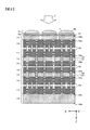
- FIG. 3 is a block diagram showing the configuration of the image sensor according to the first embodiment.
- the first substrate 111 includes a plurality of pixels 10 and a comparison unit 40 that are two-dimensionally arranged.
- a plurality of pixels 10 are arranged in the X-axis direction and the Y-axis direction shown in FIG.
- the pixel 10 outputs a photoelectric conversion signal and a noise signal, which will be described later, to the comparison unit 40.
- the comparison unit 40 is provided for each pixel 10 and includes a comparator circuit or the like.
- the comparison unit 40 compares the photoelectric conversion signal and the noise signal output from the pixel 10 with the reference signal, and outputs the comparison result to the second substrate 112.
- the second substrate 112 has a plurality of storage units 50.
- the storage unit 50 is provided for each pixel 10 and includes a latch circuit or the like.
- the storage unit 50 stores a count value corresponding to the elapsed time from the comparison start time by the comparison unit 40 as a digital signal based on the comparison result by the comparison unit 40.
- the storage unit 50 stores a digital signal corresponding to the photoelectric conversion signal and a digital signal corresponding to the noise signal.
- the storage unit 50 is also a storage unit 50 that stores a photoelectric conversion signal converted into a digital signal and a noise signal (reset signal).
- the comparison unit 40 and the storage unit 50 constitute an integration type AD conversion unit that converts a photoelectric conversion signal and a noise signal into a digital signal.
- the digital signal stored in the storage unit 50 is output to the fourth substrate 114 via the third substrate 113.
- the fourth substrate 114 has a plurality of ALUs (Arithmetic and Logic Units), that is, an arithmetic unit 80.
- the arithmetic unit 80 is provided for each pixel 10, and performs correlated double sampling (CDS) by subtraction between the digital signal of the photoelectric conversion signal and the digital signal of the noise signal, or between signals generated for each pixel 10. Perform signal processing such as computation.
- the arithmetic unit 80 includes an addition circuit, a subtraction circuit, a flip-flop circuit, a shift circuit, and the like.
- the arithmetic units 80 are connected to each other via signal lines, switches SW, and the like.
- the third substrate 113 has an ALU control unit 70 that controls the arithmetic unit 80 (hereinafter referred to as the control unit 70).
- the control unit 70 is provided for each pixel 10, and outputs a control signal to the arithmetic unit 80, the switch SW, and the like disposed on the fourth substrate 114, and controls the arithmetic contents performed by the arithmetic unit 80.
- the control unit 70 selects a pixel signal by turning on a predetermined switch SW, and the arithmetic unit 80 corresponding to the control unit 70 performs arithmetic processing on the signals of the selected plurality of pixels.
- the first substrate 111 is also a pixel substrate 111 including a plurality of pixels 10 having the photoelectric conversion unit 12 and a readout unit (output unit) described later, and the second substrate 112 is an accumulation unit 50 (storage unit 50). It is also a storage substrate 112 including The fourth substrate 114 is also an arithmetic substrate 114 that includes the arithmetic unit 80.
- correlated double sampling is performed before calculation between signals of each pixel 10. For this reason, it is possible to perform an arithmetic operation between signals of any pixel 10 using a signal from which the noise signal component for each pixel 10 is removed.
- the arithmetic unit 80 and the control unit 70 are provided so as to be stacked on the corresponding pixels 10. For this reason, it can prevent that the aperture ratio of the pixel 10 falls.
- the control unit 70 of the third substrate 113 supplies a control signal to the arithmetic unit 80 of the fourth substrate 114 from the Z-axis direction shown in FIG. As a result, it is possible to perform an operation on the signal of any pixel 10 without increasing the chip area of the image sensor 3.
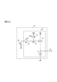
- FIG. 4 is a circuit diagram showing the configuration of the pixels of the image sensor according to the first embodiment.
- the pixel 10 includes a photoelectric conversion unit 12 such as a photodiode (PD) and a reading unit 20.
- the photoelectric conversion unit 12 has a function of converting incident light into charges and accumulating the photoelectrically converted charges.
- the reading unit 20 includes a transfer unit 13, a discharge unit 14, a floating diffusion (FD) 15, an amplification unit 16, and a current source 17.
- FD floating diffusion
- the transfer unit 13 is controlled by the signal Vtx and transfers the electric charge photoelectrically converted by the photoelectric conversion unit 12 to the floating diffusion 15. That is, the transfer unit 13 forms a charge transfer path between the photoelectric conversion unit 12 and the floating diffusion 15.
- the floating diffusion 15 holds (accumulates) electric charges.
- the amplifying unit 16 amplifies the signal based on the charge held in the floating diffusion 15 and outputs the amplified signal to the signal line 18.
- the amplifying unit 16 includes a transistor M3 whose drain terminal, gate terminal, and source terminal are connected to the power supply VDD, the floating diffusion 15, and the current source 17, respectively.
- the discharge unit (reset unit) 14 is controlled by the signal Vrst, discharges the charge of the floating diffusion 15, and resets the potential of the floating diffusion 15 to the reset potential (reference potential).
- the transfer unit 13 and the discharge unit 14 are configured by, for example, a transistor M1 and a transistor M2, respectively.
- the reading unit 20 receives a signal (photoelectric conversion signal) corresponding to the charge transferred from the photoelectric conversion unit 12 to the floating diffusion 15 by the transfer unit 13 and a signal (noise signal) when the potential of the floating diffusion 15 is reset to the reset potential. ) Are sequentially read out to the signal line 18.
- the reading unit 20 is an output unit 20 that generates and outputs a signal based on the charge accumulated in the floating diffusion 15, and the output unit 20 outputs a photoelectric conversion signal and a noise signal to the signal line 18.
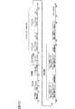
- FIG. 5 is a block diagram showing details of the configuration of the image sensor according to the first embodiment.
- the image sensor 3 includes a plurality of pixels 10, a calculation unit 100 provided for each pixel 10, a timing generator 200, a DA conversion unit 210, a global counter 220, a shift register 230, and a VSCAN circuit (vertical scanning circuit). 240, an HSCAN circuit (horizontal scanning circuit) 250, a sense amplifier 300, a line memory 310, and an input / output unit 320.
- the calculation unit 100 includes an analog / digital conversion unit (AD conversion unit) 60, a control unit 70, a calculation unit 80, a storage unit 83, a demultiplexer 81, a demultiplexer 84, and a multiplexer 85.
- AD conversion unit analog / digital conversion unit
- the AD conversion unit 60 includes a comparison unit 40, a storage unit 50, and a demultiplexer 53.
- the storage unit 50 includes a signal storage unit 51 for digital signals corresponding to the photoelectric conversion signal and a noise storage unit 52 for digital signals corresponding to the noise signal.
- the signal storage unit 51 and the noise storage unit 52 are composed of a plurality of latch circuits corresponding to the number of bits of the stored signal. For example, each of the signal storage unit 51 and the noise storage unit 52 includes 12 latch circuits, and each of the digital signals stored in the signal storage unit 51 and the noise storage unit 52 is a 12-bit parallel signal. It becomes.
- the timing generator 200 includes a plurality of circuits, and is divided into a first substrate 111 to a fourth substrate 114.
- the first substrate 111, the second substrate 112, the third substrate 113, and the fourth substrate 114 are referred to as a first layer, a second layer, a third layer, and a fourth layer, respectively.
- Each circuit constituting the timing generator 200 is disposed in the peripheral portion of the region where the pixel 10 and the arithmetic unit 100 are disposed.
- the signal storage unit 51 the noise storage unit 52, the demultiplexer 53, the DA conversion unit 210, the global counter 220, the shift register 230, and the timing generator 200 are provided. And a part of.
- the third substrate 113 is provided with a control unit 70, a VSCAN circuit 240, an HSCAN circuit 250, and a part of the timing generator 200.
- the fourth substrate 114 is provided with an arithmetic unit 80, a storage unit 83, a demultiplexer 81, a demultiplexer 84, a multiplexer 85, a sense amplifier 300, a line memory 310, and an input / output unit 320.
- the DA conversion unit 210, the global counter 220, the shift register 230, the VSCAN circuit 240, the HSCAN circuit 250, the sense amplifier 300, the line memory 310, and the input / output unit 320 are areas in which the arithmetic unit 100 is arranged on each substrate. Located in the periphery.
- the timing generator 200 is configured by a pulse generation circuit or the like, generates a pulse signal or the like based on a register setting value output from the control unit 4 of the imaging device 1, and each pixel 10, a DA conversion unit 210, a global counter 220, The data is output to the shift register 230, the VSCAN circuit 240, and the HSCAN circuit 250.
- the register setting value is set according to, for example, the shutter speed (charge accumulation time of the photoelectric conversion unit), ISO sensitivity, presence / absence of image correction, and the like.
- the DA conversion unit 210 generates a ramp signal whose signal level changes as a reference signal based on the pulse signal from the timing generator 200.
- the DA conversion unit 210 is connected in common to each comparison unit 40 provided for each pixel 10, and outputs a reference signal to each comparison unit 40.
- the global counter 220 generates a clock signal indicating the count value based on the pulse signal from the timing generator 200 and outputs the clock signal to the signal storage unit 51 and the noise storage unit 52.
- the shift register 230 generates a timing signal based on the pulse signal from the timing generator 200 and outputs the timing signal to the signal storage unit 51 and the noise storage unit 52.
- the VSCAN circuit 240 and the HSCAN circuit 250 sequentially select the respective control units 70 based on the signal from the timing generator 200, and output signals indicating the calculation contents (four arithmetic operations) performed by the calculation unit 80 and the pixel 10 to be calculated. Output to each control unit 70.
- the sense amplifier 300 is connected to the signal line 122 to which each calculation unit 100 for each pixel 10 is connected, and reads out the signal at high speed by amplifying and reading out the signal input to the signal line 122.
- the line memory 310 stores a signal read by the sense amplifier 300.
- the input / output unit 320 performs signal processing such as signal bit width adjustment and synchronization code addition on the signal output from the line memory 310, and outputs the signal to the control unit 4 of the imaging apparatus 1 as an image signal.
- the input / output unit 320 is configured by an input / output circuit or the like corresponding to a high-speed interface such as LVDS or SLVS, and transmits signals at high speed.
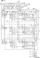
- FIG. 6 is a timing chart showing an operation example of the image sensor according to the first embodiment.
- the horizontal axis represents time.
- register settings are input to the timing generator 200 from the control unit 4 of the imaging device 1.
- the timing generator 200 generates a signal indicating the operation content of each operation unit 80 based on the register setting value, and outputs the signal to the VSCAN circuit 240, the HSCAN circuit 250, and the like.
- the VSCAN circuit 240 and the HSCAN circuit 250 sequentially output signals indicating the calculation contents and the like generated by the timing generator 200 to each control unit 70 provided for each pixel 10.
- the noise signal of each pixel 10 is output to the comparison unit 40.
- the comparison unit 40 compares the noise signal read from the pixel 10 with the reference signal supplied from the DA conversion unit 210 and outputs the comparison result to the demultiplexer 53.
- the demultiplexer 53 outputs the comparison result from the comparison unit 40 to the noise storage unit 52.
- the noise storage unit 52 Based on the comparison result from the comparison unit 40 and the clock signal from the global counter 220, the noise storage unit 52 outputs a count value corresponding to the elapsed time from the comparison start time to the comparison result output time by the comparison unit 40 as a noise signal. Is stored as a digital signal corresponding to
- the photoelectric conversion signal of each pixel 10 is output to the comparison unit 40.
- the comparison unit 40 compares the photoelectric conversion signal with the reference signal and outputs the comparison result to the demultiplexer 53.
- the demultiplexer 53 outputs the comparison result from the comparison unit 40 to the signal storage unit 51.
- the signal storage unit 51 converts the count value corresponding to the elapsed time from the comparison start time by the comparison unit 40 to the comparison result output time into a digital value corresponding to the photoelectric conversion signal Store as a signal.
- the signal storage unit 51 and the noise storage unit 52 each store a 12-bit digital signal.
- the noise storage unit 52 temporally converts the 12-bit digital signal stored in the noise storage unit 52 bit by bit based on the timing signal from the shift register 230.
- the signals are shifted and sequentially output to the signal line 121 shown in FIG.
- the serial signal output to the signal line 121 is input to the demultiplexer 81.
- the demultiplexer 81 outputs the serial signal from the noise storage unit 52 to the arithmetic unit 80.
- the arithmetic unit 80 causes the storage unit 83 to sequentially store a digital signal corresponding to the noise signal.
- the storage unit 83 stores a 12-bit digital signal related to the noise signal.
- the signal line 121 is a signal line connecting the storage unit 50 of the second substrate 112 and the demultiplexer 81 of the fourth substrate 114, and is a signal line using the through electrode 110 and bumps shown in FIG.
- the parallel signal stored in the storage unit 50 of the second substrate 112 is converted into a serial signal and output to the fourth substrate 114.
- the wiring connecting the second substrate 112 and the fourth substrate 114 can be reduced, and digital signals for the respective pixels 10 can be output simultaneously. Further, it is possible to prevent an increase in the chip area by forming a large number of through electrodes 110 and the like.
- the signal storage unit 51 converts a digital signal corresponding to the photoelectric conversion signal stored in the signal storage unit 51 into a serial signal based on the timing signal from the shift register 230. Then, the data is sequentially output to the demultiplexer 81 bit by bit via the signal line 121.
- the demultiplexer 81 outputs the serial signal from the signal storage unit 51 to the arithmetic unit 80. Based on the control signal from the control unit 70, the arithmetic unit 80 causes the demultiplexer 84 to output a 12-bit digital signal corresponding to the noise signal stored in the storage unit 83 bit by bit.
- the demultiplexer 84 outputs (feeds back) a digital signal corresponding to the noise signal to the arithmetic unit 80 based on the control signal from the control unit 70.
- the arithmetic unit 80 subtracts the digital signal corresponding to the photoelectric conversion signal output bit by bit from the signal storage unit 51 and the digital signal corresponding to the noise signal output bit by bit from the storage unit 83. A correction signal is generated.
- the arithmetic unit 80 causes the storage unit 83 to sequentially store correction signals generated for each bit.
- the arithmetic unit 80 performs subtraction a plurality of times in accordance with the number of bits of the signal stored in the storage unit 50, and sequentially stores the correction signal as a subtraction result in the storage unit 83.
- the storage unit 83 since a 12-bit digital signal is stored in each of the signal storage unit 51 and the noise storage unit 52 included in the storage unit 50, twelve subtraction processes are performed.
- the storage unit 83 stores a digital signal corresponding to a 12-bit noise signal and a 12-bit correction signal. Therefore, the storage unit 83 includes 24 latch circuits and the like.
- digital CDS for performing difference processing between the digital signal of the photoelectric conversion signal and the digital signal of the noise signal is performed in a time-sharing manner for each bit.
- the arithmetic unit 80 is provided for each pixel 10, and digital CDS is simultaneously performed on all the pixels 10. Since the digital CDS operation is performed for each bit, it is possible to avoid arranging a large number of digital circuits such as a multi-bit (for example, 12 bits) flip-flop circuit on the fourth substrate 114. As a result, the number of circuits for each pixel 10 can be reduced, and an increase in chip area can be prevented.
- the 12-bit correction signal of the pixel 10 in the region A stored in the storage unit 83 in the region A is input (feedback) to the arithmetic unit 80 in the region A via the demultiplexer 84 bit by bit.
- the 12-bit correction signal of the pixel 10 in the region B stored in the storage unit 83 in the region B passes through the demultiplexer 84 in the region B, the multiplexer 85 in the region B, and the multiplexer 85 in the region A, one bit at a time.
- the operation unit 80 in the area A calculates the 12-bit correction signal in the area A and the 12-bit correction signal in the area B input in this way bit by bit. This will be described in detail below.
- the arithmetic unit 80 in the region A outputs the 12-bit correction signal of the pixel 10 in the region A stored in the storage unit 83 in the region A to the demultiplexer 84 bit by bit.
- the demultiplexer 84 in the area A outputs (feeds back) the correction signal to the arithmetic unit 80 in the area A.
- the arithmetic unit 80 in the region B causes the demultiplexer 84 to output the correction signal for the pixel 10 in the region B stored in the storage unit 83 in the region B bit by bit.
- the demultiplexer 84 in the area B outputs the correction signal to the multiplexer 85 in the area B.
- a signal line 123 and a signal line 124 to which each arithmetic unit 100 is connected are connected to each multiplexer 85 provided for each pixel 10.
- the signal line 123 and the signal line 124 are two-dimensionally arranged in the row direction and the column direction on the fourth substrate 114, and are connected to each arithmetic unit 100 for each pixel 10.
- the multiplexer 85 is controlled by the control unit 70 and selects a signal to be calculated by the calculation unit 80 from the correction signals input to the signal line 123 and the signal line 124.
- the multiplexer 85 in the region B outputs the correction signal for the pixel 10 in the region B to the multiplexer 85 in the region A via the signal line 123 shown in FIG.
- the multiplexer 85 in the region A outputs the correction signal for the pixel 10 in the region B to the arithmetic unit 80 in the region A via the signal line 124.
- the correction signal for the pixel 10 in the region A and the correction signal for the pixel 10 in the region B are sequentially input to the arithmetic unit 80 in the region A for each bit.
- the arithmetic unit 80 in the area A performs an operation on the correction signal output bit by bit from the storage unit 83 in the area A and the correction signal output bit by bit from the storage unit 83 in the area B, and outputs the pixel signal. Generate.
- the arithmetic unit 80 causes the storage unit 83 to sequentially store pixel signals generated for each bit.
- the calculation unit 80 performs a plurality of calculations according to the number of bits of the correction signal, and sequentially stores pixel signals that are the calculation results in the storage unit 83.
- the storage unit 83 stores a 12-bit correction signal and a 12-bit pixel signal after calculation between the correction signals.
- the correction signal is generated by performing the correlated double sampling before the calculation between the correction signals of each pixel 10. For this reason, it is possible to perform an arithmetic operation between correction signals of arbitrary pixels 10 using a signal from which a noise signal component for each pixel 10 is removed. In the present embodiment, calculation between correction signals generated for each pixel 10 is performed for each bit. As a result, it is possible to avoid arranging a multi-bit digital circuit such as a multi-bit (for example, 12-bit) arithmetic operation circuit or a multi-bit (for example, 12-bit) flip-flop circuit on the fourth substrate 114, and the chip area can be reduced. It can be prevented from increasing.
- a multi-bit digital circuit such as a multi-bit (for example, 12-bit) arithmetic operation circuit or a multi-bit (for example, 12-bit) flip-flop circuit
- the circuit area of the calculation unit 80 can be reduced. Further, the arithmetic unit 80 performs correlated double sampling and calculates between correction signals for each pixel 10. That is, the calculation unit 80 is a correction / inter-pixel calculation unit that serves as both a correction unit that generates a correction signal by subtraction between digital signals and an inter-pixel calculation unit that performs calculation between correction signals generated for each pixel 10. Function as. For this reason, a chip area can be reduced compared with the case where a correction
- the fourth substrate 114 is different from the third substrate 113 on which the control unit 70 is disposed, and the arithmetic unit 80, the multiplexer 85, and the like are disposed on the fourth substrate 114.
- the signal line 123 and the signal line 124 can be two-dimensionally arranged and commonly connected to the arithmetic units 100 of all the pixels 10 without increasing the chip area.
- the correction signal of the other pixel 10 on which the calculation unit 100 performs calculation is directly transmitted through the signal line 123 and the signal line 124 without using a latch or a register. Since a delay time for passing through a latch, a register, or the like does not occur, a signal can be read out at high speed, and an operation between arbitrary pixels 10 can be performed at high speed.
- the arithmetic unit 80 causes the demultiplexer 84 to output the pixel signal stored in the storage unit 83.
- the demultiplexer 84 outputs the pixel signal to the signal line 122.
- the sense amplifier 300 amplifies and reads out the pixel signal output to the signal line 122.
- Each calculation unit 100 provided for each pixel 10 sequentially outputs a signal to the signal line 122, and the sense amplifier 300 sequentially reads the signal output to the signal line 122.
- the pixel signals read by the sense amplifier 300 are sequentially stored in the line memory 310.
- the input / output unit 320 performs signal processing on signals sequentially output from the line memory 310, and outputs the signal after signal processing as an image signal.
- the image pickup device 3 is provided for each of the pixels 10 having the photoelectric conversion unit 12 and the photoelectric conversion signal output from the pixel 10 and the noise signal output from the pixel 10. And a calculation unit 100 that performs calculation between correction signals generated for each pixel 10.
- a correction signal is generated by performing correlated double sampling before calculation between signals of each pixel 10. For this reason, it is possible to perform an arithmetic operation between signals of any pixel 10 using a signal from which the noise signal component for each pixel 10 is removed.
- the arithmetic unit 100 converts the photoelectric conversion signal into the first digital signal and converts the noise signal into the second digital signal, and the correction signal by subtraction between the first digital signal and the second digital signal.
- a correction / inter-pixel calculation unit (arithmetic unit 80) for performing calculation between correction signals generated for each pixel 10. Since it did in this way, compared with the case where a correction
- the photoelectric conversion unit 12 is disposed on the first substrate, and at least a part of the arithmetic unit 100 is disposed on the second substrate. Since it did in this way, it can prevent that the aperture ratio of the pixel 10 falls.
- the AD conversion unit 60 converts the photoelectric conversion signal into a first digital signal having a first number of bits, and converts the noise signal into a second digital signal having a second number of bits. Since it did in this way, each of a photoelectric conversion signal and a noise signal can be converted into a digital signal, and can be memorize
- the computing unit 100 includes a storage unit 83 that stores the second digital signal having the second number of bits.
- the calculation unit 100 performs subtraction between the stored second digital signal and the first digital signal output from the AD conversion unit 60 for each bit.
- difference processing between the digital signal of the photoelectric conversion signal and the digital signal of the noise signal is performed for each bit. Since it did in this way, providing many flip-flop circuits etc. for every pixel 10 can be avoided, and it can prevent that a chip area increases.
- the computing unit 100 performs computation between correction signals generated for each pixel 10 for each bit. Since it did in this way, it can avoid providing many four arithmetic operation circuits, a flip-flop circuit, etc. for the calculation between pixels which calculates between the signals of each pixel 10, and can prevent that a chip area increases. .
- the imaging device 3 further includes a plurality of signal lines (a signal line 123 and a signal line 124) to which a plurality of calculation units 100 are connected and from which the correction signal is output.
- the calculation unit 100 includes a first selection unit (multiplexer 85) that selects a correction signal to be calculated by the calculation unit 100 from correction signals output to a plurality of signal lines.
- the control unit 70 controls the arithmetic unit 80 and the multiplexer 85 to select and read out the correction signal for each pixel 10. For this reason, the calculation between the correction signals of arbitrary pixels 10 can be performed.
- the imaging device 3 includes a plurality of pixels 10 having a photoelectric conversion unit 12 that photoelectrically converts incident light to generate charges and an output unit 20 (reading unit 20) that generates and outputs a signal based on the charges.
- a correction signal is generated by the substrate (first substrate 111), the reset signal after resetting the charge of the output unit 20, and the photoelectric conversion signal based on the charge generated by the photoelectric conversion unit 12, and is generated for each pixel 10.
- an arithmetic substrate (fourth substrate 114) that is stacked on the pixel substrate. Since it did in this way, the calculation between the signals of arbitrary pixels 10 can be performed using the signal from which the noise signal component for each pixel 10 is removed.
- the imaging device 3 includes a storage substrate (second substrate 112) including a storage unit (storage unit 50) that stores the photoelectric conversion signal converted into the digital signal and the reset signal.
- the storage substrate is stacked between the pixel substrate and the arithmetic substrate. Since it did in this way, it can prevent that the aperture ratio of the pixel 10 falls.
- Modification 1 In the above-described embodiment, the example in which the arithmetic unit 80 is shared by the correction unit that performs the CDS process and the inter-pixel calculation that performs the inter-pixel calculation has been described. However, as illustrated in FIG. 7, the correction unit 54 that performs the CDS process may be provided separately from the arithmetic unit 80. In this case, the arithmetic unit 80 functions as an inter-pixel arithmetic unit.
- the correction unit 54 generates a correction signal by subtracting the digital signal based on the photoelectric conversion signal output from the signal storage unit 51 and the digital signal based on the noise signal output from the noise storage unit 52, and To the arithmetic unit 80.
- Modification 2 In the above-described embodiment, the example in which the pixel signal that is the result of the inter-pixel calculation is sequentially output to the sense amplifier 300 via the signal line 122 has been described. However, the arithmetic unit 100 may output the correction signal stored in the storage unit 83 to the sense amplifier 300 via the signal line 122 as a pixel signal. In addition, a digital signal corresponding to the photoelectric conversion signal stored in the signal storage unit 51 and a digital signal corresponding to the noise signal stored in the noise storage unit 52 are respectively connected to the signal line 122 via the demultiplexer 81. May be output.
- control unit 70 may control the arithmetic unit 80 and the like to perform arithmetic operations for each number of bits.
- the calculation may be performed every two bits, or may be performed every number of bits smaller than the number of bits of the digital signal stored in the noise storage unit 52.
- Modification 4 In the above-described embodiment, an example in which digital CDS is performed before calculation between signals of each pixel 10 has been described. However, analog CDS may be performed before calculation between signals of each pixel 10.
- the AD converter 60 performs a difference process between the photoelectric conversion signal and the noise signal, and converts an analog signal based on the difference between the signals into a digital signal.
- the storage unit 50 stores a digital signal from which a noise signal component for each pixel 10 is removed. The digital signals stored in the storage unit 50 are sequentially output to the arithmetic unit 80.
Landscapes
- Engineering & Computer Science (AREA)
- Physics & Mathematics (AREA)
- Power Engineering (AREA)
- Multimedia (AREA)
- Signal Processing (AREA)
- Electromagnetism (AREA)
- Condensed Matter Physics & Semiconductors (AREA)
- General Physics & Mathematics (AREA)
- Computer Hardware Design (AREA)
- Microelectronics & Electronic Packaging (AREA)
- Transforming Light Signals Into Electric Signals (AREA)
- Solid State Image Pick-Up Elements (AREA)
Abstract
Description
本発明の第2の態様によると、撮像素子は、光電変換部及び出力部を有する複数の画素が配置される画素基板と、前記出力部をリセットした後の信号をデジタル変換されたリセット信号と、前記光電変換部で光電変換された信号に基づくデジタル変換された光電変換信号とによって補正信号を生成し、前記画素毎に生成される前記補正信号を用いた演算を行う演算部が前記画素毎に設けられる演算基板と、を有し、前記画素基板と前記演算基板とが積層して配置される。
本発明の第3の態様によると、撮像装置は、第1または第2の態様による撮像素子と、前記画素からの信号に基づいて画像データを生成する画像生成部と、を備える。
図1は、第1の実施の形態に係る撮像装置の構成を示すブロック図である。撮像装置1は、撮影光学系2、撮像素子3、および制御部4を備える。撮像装置1は、例えばカメラである。撮影光学系2は、撮像素子3上に被写体像を結像する。撮像素子3は、撮影光学系2により形成された被写体像を撮像して画像信号を生成する。撮像素子3は、例えばCMOSイメージセンサである。制御部4は、撮像素子3の動作を制御するための制御信号を撮像素子3に出力する。また、制御部4は、撮像素子3から出力された画像信号に対して各種の画像処理を施し、画像データを生成する画像生成部として機能する。なお、撮影光学系2は、撮像装置1から着脱可能にしてもよい。
(1)撮像素子3は、光電変換部12を有する複数の画素10と、画素10毎に設けられ、画素10から出力される光電変換信号と画素10から出力されるノイズ信号とによって補正信号を生成し、画素10毎に生成される補正信号間の演算を行う演算部100と、を備える。本実施の形態では、各画素10の信号間の演算前に、相関二重サンプリングを行って補正信号を生成する。このため、画素10毎のノイズ信号成分を除去した信号を用いて、任意の画素10の信号間の演算を行うことができる。
(2)演算部100は、光電変換信号を第1デジタル信号に変換しノイズ信号を第2デジタル信号に変換するAD変換部60と、第1デジタル信号と第2デジタル信号との減算によって補正信号を生成し、画素10毎に生成される補正信号間の演算を行う補正・画素間演算部(演算ユニット80)と、を有する。このようにしたので、補正部および画素間演算部を別々に設ける場合と比較して、画素10毎の周辺回路の面積を低減することができ、チップ面積を低減することができる。
(4)AD変換部60は、光電変換信号を第1のビット数の第1デジタル信号に変換し、ノイズ信号を第2のビット数の第2デジタル信号に変換する。このようにしたので、光電変換信号およびノイズ信号の各々をデジタル信号に変換して、記憶部50に記憶させることができる。
(5)演算部100は、第2のビット数の第2デジタル信号を記憶する記憶部83を有する。演算部100は、記憶された第2デジタル信号とAD変換部60から出力される第1デジタル信号との減算を、1ビット毎に行う。本実施の形態では、光電変換信号のデジタル信号とノイズ信号のデジタル信号との差分処理を1ビット毎に行う。このようにしたので、多数のフリップフロップ回路等を画素10毎に設けることを回避でき、チップ面積が増大することを防ぐことができる。
(7)撮像素子3は、複数の演算部100が接続され、演算部100から補正信号が出力される複数の信号線(信号線123および信号線124)を更に備える。演算部100は、演算部100が演算を行う補正信号を複数の信号線に出力された補正信号から選択する第1選択部(マルチプレクサ85)を有する。本実施の形態では、制御部70により演算ユニット80およびマルチプレクサ85を制御して、各画素10の補正信号を選択して読み出す。このため、任意の画素10の補正信号間の演算を行うことができる。
(9)撮像素子3は、デジタル信号に変換された光電変換信号及びリセット信号とを蓄積する蓄積部(記憶部50)を含む蓄積基板(第2基板112)を有する。蓄積基板は、画素基板と演算基板の間に積層して配置される。このようにしたので、画素10の開口率が低下することを防ぐことができる。
上述した実施の形態では、演算ユニット80がCDS処理を行う補正部と画素間演算を行う画素間演算とに共用される例について説明した。しかし、図7に示すように、CDS処理を行う補正部54を、演算ユニット80とは別に設けるようにしてもよい。この場合、演算ユニット80は、画素間演算部として機能する。補正部54は、信号用記憶部51から出力される光電変換信号によるデジタル信号と、ノイズ用記憶部52から出力されるノイズ信号によるデジタル信号との減算によって補正信号を生成し、デマルチプレクサ81を介して演算ユニット80に出力する。
上述した実施の形態では、画素間演算の結果となる画素信号を、信号線122を介してセンスアンプ300に順次出力する例について説明した。しかし、演算部100は、記憶部83に記憶された補正信号を、画素信号として信号線122を介してセンスアンプ300に出力するようにしてもよい。また、信号用記憶部51に記憶された光電変換信号に応じたデジタル信号、およびノイズ用記憶部52に記憶されたノイズ信号に応じたデジタル信号の各々を、デマルチプレクサ81を介して信号線122に出力するようにしてもよい。
上述した実施の形態では、CDS処理および画素間演算を1ビット毎に時分割的に行う例について説明した。しかし、制御部70により演算ユニット80等を制御して、複数ビット数毎に演算を行うようにしてもよい。例えば、2ビット毎に演算を行うようにしてもよいし、ノイズ用記憶部52に記憶されるデジタル信号のビット数より少ないビット数毎に行うようにしてもよい。
上述した実施の形態では、各画素10の信号間の演算前にデジタルCDSを行う例について説明した。しかし、各画素10の信号間の演算前にアナログCDSを行うようにしてもよい。例えば、AD変換部60において、光電変換信号とノイズ信号との差分処理を行って、信号間の差分に基づくアナログ信号をデジタル信号に変換する。記憶部50には、画素10毎のノイズ信号成分を除去したデジタル信号が記憶される。記憶部50に記憶されたデジタル信号は、演算ユニット80に順次出力される。
上述した実施の形態では、光電変換部12としてフォトダイオードを用いる例について説明した。しかし、光電変換部12として光電変換膜を用いるようにしてもよい。
日本国特許出願2016年第60001号(2016年3月24日出願)
Claims (15)
- 入射光を光電変換し電荷を生成する光電変換部及び前記電荷に基づく信号を生成し出力する出力部とを有する複数の画素を含む画素基板と、
前記出力部の前記電荷をリセットした後のリセット信号と前記光電変換部で生成された電荷に基づく光電変換信号とによって補正信号を生成し、前記画素毎に生成される補正信号間の演算を行う演算部を含み、前記画素基板に積層される演算基板と、
を有する撮像素子。 - 請求項1に記載の撮像素子において、
前記演算部は、前記画素毎に設けられる撮像素子。 - 光電変換部及び出力部を有する複数の画素が配置される画素基板と、
前記出力部をリセットした後の信号をデジタル変換されたリセット信号と、前記光電変換部で光電変換された信号に基づくデジタル変換された光電変換信号とによって補正信号を生成し、前記画素毎に生成される前記補正信号を用いた演算を行う演算部が前記画素毎に設けられる演算基板と、を有し、
前記画素基板と前記演算基板とが積層して配置される撮像素子。 - 請求項1から請求項3までのいずれか一項に記載の撮像素子において、
デジタル信号に変換された前記光電変換信号及び前記リセット信号とを蓄積する蓄積部を含む蓄積基板を有し、
前記蓄積基板は、前記画素基板と前記演算基板の間に積層して配置される撮像素子。 - 請求項4に記載の撮像素子において、
前記画素基板、前記蓄積基板、及び、前記演算基板は、配線層が配置される第1面と、前記第1面とは反対側の第2面とを有し、
前記蓄積基板、及び、前記演算基板は、前記第1面から前記第2面まで貫通する貫通孔と、前記第1面から前記貫通孔を介して前記第2面まで配置される貫通電極とを有し、
前記画素基板と前記蓄積基板は、互いに前記第1面で電気的に接続され、
前記蓄積基板と前記演算基板は、互いに前記第2面で電気的に接続される撮像素子。 - 請求項5に記載の撮像素子において、
電荷に基づく信号をデジタル信号に変換し、前記電荷をリセットした後の信号をデジタル信号に変換するAD変換部を有する撮像素子。 - 請求項5または請求項6に記載の撮像素子において、
前記蓄積基板に蓄積される前記デジタル信号は、第1のビット数を有し、
前記演算部は、蓄積された前記光電変換信号のデジタル信号と前記リセット信号のデジタル信号との減算を、前記第1のビット数より少ないビット数毎に行う撮像素子。 - 請求項5から請求項7までのいずれか一項に記載の撮像素子において、
前記蓄積基板に蓄積される前記デジタル信号は、第1のビット数を有し、
前記蓄積基板から前記演算基板に出力される前記デジタル信号は、前記第1のビット数より小さい第2のビット数毎に出力され、
前記演算部は、蓄積された前記光電変換信号のデジタル信号と前記リセット信号のデジタル信号との減算を、前記第2のビット数毎に行う撮像素子。 - 請求項1から請求項8までのいずれか一項に記載の撮像素子において、
前記演算部は、前記光電変換信号のデジタル信号と前記リセット信号のデジタル信号との減算によって前記補正信号を生成する補正部と、前記画素毎に生成される補正信号間の演算を行う画素間演算部と、を有する撮像素子。 - 請求項1から請求項8までのいずれか一項に記載の撮像素子において、
前記演算部は、前記光電変換信号のデジタル信号と前記リセット信号のデジタル信号との減算によって前記補正信号を生成し、前記画素毎に生成される補正信号間の演算を行う補正・画素間演算部と、を有する撮像素子。 - 請求項1から請求項10までのいずれか一項に記載の撮像素子において、
前記演算部は、前記光電変換信号のデジタル信号と前記リセット信号のデジタル信号との減算を、1ビット毎に行う撮像素子。 - 請求項1から請求項11までのいずれか一項に記載の撮像素子において、
前記演算部は、前記画素毎に生成される補正信号間の演算を、1ビット毎に行う撮像素子。 - 請求項1から請求項12までのいずれか一項に記載の撮像素子において、
複数の前記演算部が接続され、前記演算部から前記補正信号が出力される複数の信号線を更に備え、
前記演算部は、前記演算部が演算を行う前記補正信号を前記複数の信号線に出力された前記補正信号から選択する第1選択部を有する撮像素子。 - 請求項13に記載の撮像素子において、
前記演算部は、前記補正信号を前記信号線に出力するか否かを選択する第2選択部を有する撮像素子。 - 請求項1から請求項14までのいずれか一項に記載の撮像素子と、
前記画素からの信号に基づいて画像データを生成する画像生成部と、を備える撮像装置。
Priority Applications (6)
| Application Number | Priority Date | Filing Date | Title |
|---|---|---|---|
| EP17769819.8A EP3435658B1 (en) | 2016-03-24 | 2017-02-27 | Imaging element and imaging device |
| US16/085,160 US10879298B2 (en) | 2016-03-24 | 2017-02-27 | Image sensor and image capturing device |
| CN201780032301.4A CN109155832B (zh) | 2016-03-24 | 2017-02-27 | 摄像元件和摄像装置 |
| JP2018507162A JP6822468B2 (ja) | 2016-03-24 | 2017-02-27 | 撮像素子および撮像装置 |
| US16/953,525 US11557624B2 (en) | 2016-03-24 | 2020-11-20 | Image sensor and image capturing device |
| US18/080,865 US11978757B2 (en) | 2016-03-24 | 2022-12-14 | Image sensor and image capturing device |
Applications Claiming Priority (2)
| Application Number | Priority Date | Filing Date | Title |
|---|---|---|---|
| JP2016-060001 | 2016-03-24 | ||
| JP2016060001 | 2016-03-24 |
Related Child Applications (2)
| Application Number | Title | Priority Date | Filing Date |
|---|---|---|---|
| US16/085,160 A-371-Of-International US10879298B2 (en) | 2016-03-24 | 2017-02-27 | Image sensor and image capturing device |
| US16/953,525 Division US11557624B2 (en) | 2016-03-24 | 2020-11-20 | Image sensor and image capturing device |
Publications (1)
| Publication Number | Publication Date |
|---|---|
| WO2017163774A1 true WO2017163774A1 (ja) | 2017-09-28 |
Family
ID=59900001
Family Applications (1)
| Application Number | Title | Priority Date | Filing Date |
|---|---|---|---|
| PCT/JP2017/007549 WO2017163774A1 (ja) | 2016-03-24 | 2017-02-27 | 撮像素子および撮像装置 |
Country Status (5)
| Country | Link |
|---|---|
| US (3) | US10879298B2 (ja) |
| EP (1) | EP3435658B1 (ja) |
| JP (3) | JP6822468B2 (ja) |
| CN (4) | CN113225497A (ja) |
| WO (1) | WO2017163774A1 (ja) |
Cited By (2)
| Publication number | Priority date | Publication date | Assignee | Title |
|---|---|---|---|---|
| EP3439289A4 (en) * | 2016-03-29 | 2019-09-18 | Nikon Corporation | IMAGING ELEMENT AND IMAGING DEVICE |
| EP3439039A4 (en) * | 2016-03-31 | 2019-09-18 | Nikon Corporation | IMAGING ELEMENT AND IMAGING DEVICE |
Families Citing this family (2)
| Publication number | Priority date | Publication date | Assignee | Title |
|---|---|---|---|---|
| KR20210150594A (ko) * | 2019-05-10 | 2021-12-10 | 소니 어드밴스드 비주얼 센싱 아게 | 이미지 센서 픽셀에 대한 nmos 비교기 |
| JP2022100947A (ja) * | 2020-12-24 | 2022-07-06 | キヤノン株式会社 | 光電変換装置、光電変換システム、移動体 |
Citations (3)
| Publication number | Priority date | Publication date | Assignee | Title |
|---|---|---|---|---|
| JP2006186862A (ja) * | 2004-12-28 | 2006-07-13 | Nidec Copal Corp | 画像読取装置 |
| JP2011172121A (ja) * | 2010-02-19 | 2011-09-01 | Sony Corp | 固体撮像素子およびカメラシステム |
| JP2015041838A (ja) * | 2013-08-21 | 2015-03-02 | 株式会社ニコン | 撮像素子および撮像装置 |
Family Cites Families (31)
| Publication number | Priority date | Publication date | Assignee | Title |
|---|---|---|---|---|
| JP2001094888A (ja) * | 1999-09-22 | 2001-04-06 | Canon Inc | 撮像装置 |
| JP3959925B2 (ja) | 2000-04-10 | 2007-08-15 | ソニー株式会社 | 画像処理装置及び撮像素子 |
| US6741198B2 (en) * | 2001-06-20 | 2004-05-25 | R3 Logic, Inc. | High resolution, low power, wide dynamic range imager with embedded pixel processor and DRAM storage |
| KR100782463B1 (ko) | 2005-04-13 | 2007-12-05 | (주)실리콘화일 | 3차원 구조를 갖는 이미지 센서의 분리형 단위화소 및 그제조방법 |
| EP2190185B1 (en) * | 2007-09-05 | 2013-11-06 | Tohoku University | Solid-state image sensor |
| JP5178458B2 (ja) * | 2008-10-31 | 2013-04-10 | キヤノン株式会社 | 固体撮像装置、撮像システム、および、固体撮像装置の駆動方法 |
| JP4835710B2 (ja) * | 2009-03-17 | 2011-12-14 | ソニー株式会社 | 固体撮像装置、固体撮像装置の製造方法、固体撮像装置の駆動方法、及び電子機器 |
| JP5685898B2 (ja) | 2010-01-08 | 2015-03-18 | ソニー株式会社 | 半導体装置、固体撮像装置、およびカメラシステム |
| WO2011156887A1 (en) * | 2010-06-17 | 2011-12-22 | Mosaid Technologies Incorporated | Semiconductor device with through-silicon vias |
| JP6041495B2 (ja) * | 2011-03-24 | 2016-12-07 | キヤノン株式会社 | 撮像装置及び欠陥画素の判定方法 |
| US8637800B2 (en) * | 2011-04-19 | 2014-01-28 | Altasens, Inc. | Image sensor with hybrid heterostructure |
| JP5820620B2 (ja) | 2011-05-25 | 2015-11-24 | オリンパス株式会社 | 固体撮像装置、撮像装置、および信号読み出し方法 |
| JP2013090139A (ja) | 2011-10-18 | 2013-05-13 | Sony Corp | 撮像素子およびカメラシステム |
| JP6021360B2 (ja) | 2012-03-07 | 2016-11-09 | キヤノン株式会社 | 撮像装置、撮像システム、および撮像装置の駆動方法。 |
| US8957358B2 (en) * | 2012-04-27 | 2015-02-17 | Taiwan Semiconductor Manufacturing Company, Ltd. | CMOS image sensor chips with stacked scheme and methods for forming the same |
| RU2018109081A (ru) * | 2012-05-02 | 2019-02-26 | Никон Корпорейшн | Устройство формирования изображений |
| TWI583195B (zh) | 2012-07-06 | 2017-05-11 | 新力股份有限公司 | A solid-state imaging device and a solid-state imaging device, and an electronic device |
| JP2014060573A (ja) * | 2012-09-18 | 2014-04-03 | Sony Corp | 固体撮像素子、制御方法、および電子機器 |
| JP6164869B2 (ja) * | 2013-02-26 | 2017-07-19 | キヤノン株式会社 | 撮像装置、撮像システム、撮像装置の駆動方法 |
| JP2015023391A (ja) | 2013-07-18 | 2015-02-02 | 株式会社ニコン | 固体撮像装置 |
| CN110365899B (zh) * | 2013-09-30 | 2022-03-22 | 株式会社尼康 | 电子设备 |
| KR102104564B1 (ko) * | 2013-11-21 | 2020-04-24 | 삼성전자주식회사 | 디지털 상관 이중 샘플링 회로 및 이를 포함하는 이미지 센서 |
| JP2015109502A (ja) * | 2013-12-03 | 2015-06-11 | ソニー株式会社 | イメージセンサおよびイメージセンサの動作方法、撮像装置、電子機器、並びにプログラム |
| JP2015109503A (ja) * | 2013-12-03 | 2015-06-11 | ソニー株式会社 | イメージセンサおよびイメージセンサの動作方法、撮像装置、電子機器、並びにプログラム |
| JP6314477B2 (ja) | 2013-12-26 | 2018-04-25 | ソニー株式会社 | 電子デバイス |
| JP6407083B2 (ja) * | 2015-03-30 | 2018-10-17 | キヤノン株式会社 | 光電変換装置、および、光電変換システム |
| US10896923B2 (en) * | 2015-09-18 | 2021-01-19 | Semiconductor Energy Laboratory Co., Ltd. | Method of operating an imaging device with global shutter system |
| US10020336B2 (en) * | 2015-12-28 | 2018-07-10 | Semiconductor Energy Laboratory Co., Ltd. | Imaging device and electronic device using three dimentional (3D) integration |
| CN113923389A (zh) | 2016-03-29 | 2022-01-11 | 株式会社尼康 | 摄像元件 |
| CN116995084A (zh) | 2016-03-31 | 2023-11-03 | 株式会社尼康 | 摄像元件以及摄像装置 |
| KR102527110B1 (ko) * | 2016-05-23 | 2023-05-03 | 에스케이하이닉스 주식회사 | 아날로그-디지털 변환 장치 및 그 동작 방법 |
-
2017
- 2017-02-27 US US16/085,160 patent/US10879298B2/en active Active
- 2017-02-27 CN CN202110447255.2A patent/CN113225497A/zh active Pending
- 2017-02-27 EP EP17769819.8A patent/EP3435658B1/en active Active
- 2017-02-27 CN CN202110447278.3A patent/CN113225498A/zh active Pending
- 2017-02-27 JP JP2018507162A patent/JP6822468B2/ja active Active
- 2017-02-27 WO PCT/JP2017/007549 patent/WO2017163774A1/ja active Application Filing
- 2017-02-27 CN CN202110446873.5A patent/CN113225496A/zh active Pending
- 2017-02-27 CN CN201780032301.4A patent/CN109155832B/zh active Active
-
2020
- 2020-11-20 US US16/953,525 patent/US11557624B2/en active Active
-
2021
- 2021-01-04 JP JP2021000247A patent/JP7310837B2/ja active Active
-
2022
- 2022-12-14 US US18/080,865 patent/US11978757B2/en active Active
-
2023
- 2023-06-19 JP JP2023099943A patent/JP2023123602A/ja active Pending
Patent Citations (3)
| Publication number | Priority date | Publication date | Assignee | Title |
|---|---|---|---|---|
| JP2006186862A (ja) * | 2004-12-28 | 2006-07-13 | Nidec Copal Corp | 画像読取装置 |
| JP2011172121A (ja) * | 2010-02-19 | 2011-09-01 | Sony Corp | 固体撮像素子およびカメラシステム |
| JP2015041838A (ja) * | 2013-08-21 | 2015-03-02 | 株式会社ニコン | 撮像素子および撮像装置 |
Cited By (8)
| Publication number | Priority date | Publication date | Assignee | Title |
|---|---|---|---|---|
| EP3439289A4 (en) * | 2016-03-29 | 2019-09-18 | Nikon Corporation | IMAGING ELEMENT AND IMAGING DEVICE |
| US10998367B2 (en) | 2016-03-29 | 2021-05-04 | Nikon Corporation | Image sensor and image-capturing apparatus |
| US11652128B2 (en) | 2016-03-29 | 2023-05-16 | Nikon Corporation | Image sensor and image-capturing apparatus |
| EP3439039A4 (en) * | 2016-03-31 | 2019-09-18 | Nikon Corporation | IMAGING ELEMENT AND IMAGING DEVICE |
| US10720465B2 (en) | 2016-03-31 | 2020-07-21 | Nikon Corporation | Image sensor and image capture device |
| US20200258934A1 (en) | 2016-03-31 | 2020-08-13 | Nikon Corporation | Image sensor and image capture device |
| US11177312B2 (en) | 2016-03-31 | 2021-11-16 | Nikon Corporation | Image sensor and image capture device |
| US11682690B2 (en) | 2016-03-31 | 2023-06-20 | Nikon Corporation | Image sensor and image capture device |
Also Published As
| Publication number | Publication date |
|---|---|
| US11978757B2 (en) | 2024-05-07 |
| CN113225496A (zh) | 2021-08-06 |
| JP2023123602A (ja) | 2023-09-05 |
| CN109155832A (zh) | 2019-01-04 |
| JP7310837B2 (ja) | 2023-07-19 |
| US20210074746A1 (en) | 2021-03-11 |
| JPWO2017163774A1 (ja) | 2019-01-31 |
| US11557624B2 (en) | 2023-01-17 |
| JP2021061438A (ja) | 2021-04-15 |
| EP3435658A1 (en) | 2019-01-30 |
| JP6822468B2 (ja) | 2021-01-27 |
| CN113225497A (zh) | 2021-08-06 |
| US10879298B2 (en) | 2020-12-29 |
| US20190081093A1 (en) | 2019-03-14 |
| EP3435658B1 (en) | 2024-01-03 |
| CN109155832B (zh) | 2021-05-14 |
| CN113225498A (zh) | 2021-08-06 |
| US20230111474A1 (en) | 2023-04-13 |
| EP3435658A4 (en) | 2019-09-18 |
Similar Documents
| Publication | Publication Date | Title |
|---|---|---|
| US11652128B2 (en) | Image sensor and image-capturing apparatus | |
| JP2022046686A (ja) | 撮像素子および撮像装置 | |
| JP7310837B2 (ja) | 撮像素子および撮像装置 | |
| WO2017169478A1 (ja) | 撮像素子および撮像装置 | |
| JP2023181484A (ja) | 撮像素子 | |
| JP7491335B2 (ja) | 撮像素子、及び撮像装置 | |
| US20210074756A1 (en) | Image sensor and image-capturing apparatus | |
| JP2018033146A (ja) | 固体撮像装置および電子カメラ |
Legal Events
| Date | Code | Title | Description |
|---|---|---|---|
| WWE | Wipo information: entry into national phase |
Ref document number: 2018507162 Country of ref document: JP |
|
| NENP | Non-entry into the national phase |
Ref country code: DE |
|
| WWE | Wipo information: entry into national phase |
Ref document number: 2017769819 Country of ref document: EP |
|
| ENP | Entry into the national phase |
Ref document number: 2017769819 Country of ref document: EP Effective date: 20181024 |
|
| 121 | Ep: the epo has been informed by wipo that ep was designated in this application |
Ref document number: 17769819 Country of ref document: EP Kind code of ref document: A1 |