WO2017150469A1 - 撮像素子および撮像装置 - Google Patents
撮像素子および撮像装置 Download PDFInfo
- Publication number
- WO2017150469A1 WO2017150469A1 PCT/JP2017/007548 JP2017007548W WO2017150469A1 WO 2017150469 A1 WO2017150469 A1 WO 2017150469A1 JP 2017007548 W JP2017007548 W JP 2017007548W WO 2017150469 A1 WO2017150469 A1 WO 2017150469A1
- Authority
- WO
- WIPO (PCT)
- Prior art keywords
- unit
- signal
- storage unit
- pixels
- output
- Prior art date
- Legal status (The legal status is an assumption and is not a legal conclusion. Google has not performed a legal analysis and makes no representation as to the accuracy of the status listed.)
- Ceased
Links
Images


Classifications
-
- H—ELECTRICITY
- H10—SEMICONDUCTOR DEVICES; ELECTRIC SOLID-STATE DEVICES NOT OTHERWISE PROVIDED FOR
- H10F—INORGANIC SEMICONDUCTOR DEVICES SENSITIVE TO INFRARED RADIATION, LIGHT, ELECTROMAGNETIC RADIATION OF SHORTER WAVELENGTH OR CORPUSCULAR RADIATION
- H10F39/00—Integrated devices, or assemblies of multiple devices, comprising at least one element covered by group H10F30/00, e.g. radiation detectors comprising photodiode arrays
- H10F39/80—Constructional details of image sensors
- H10F39/811—Interconnections
-
- H—ELECTRICITY
- H04—ELECTRIC COMMUNICATION TECHNIQUE
- H04N—PICTORIAL COMMUNICATION, e.g. TELEVISION
- H04N25/00—Circuitry of solid-state image sensors [SSIS]; Control thereof
- H04N25/60—Noise processing, e.g. detecting, correcting, reducing or removing noise
- H04N25/65—Noise processing, e.g. detecting, correcting, reducing or removing noise applied to reset noise, e.g. KTC noise related to CMOS structures by techniques other than CDS
-
- H—ELECTRICITY
- H04—ELECTRIC COMMUNICATION TECHNIQUE
- H04N—PICTORIAL COMMUNICATION, e.g. TELEVISION
- H04N25/00—Circuitry of solid-state image sensors [SSIS]; Control thereof
- H04N25/60—Noise processing, e.g. detecting, correcting, reducing or removing noise
- H04N25/617—Noise processing, e.g. detecting, correcting, reducing or removing noise for reducing electromagnetic interference, e.g. clocking noise
-
- H—ELECTRICITY
- H04—ELECTRIC COMMUNICATION TECHNIQUE
- H04N—PICTORIAL COMMUNICATION, e.g. TELEVISION
- H04N25/00—Circuitry of solid-state image sensors [SSIS]; Control thereof
- H04N25/70—SSIS architectures; Circuits associated therewith
- H04N25/71—Charge-coupled device [CCD] sensors; Charge-transfer registers specially adapted for CCD sensors
- H04N25/75—Circuitry for providing, modifying or processing image signals from the pixel array
-
- H—ELECTRICITY
- H04—ELECTRIC COMMUNICATION TECHNIQUE
- H04N—PICTORIAL COMMUNICATION, e.g. TELEVISION
- H04N25/00—Circuitry of solid-state image sensors [SSIS]; Control thereof
- H04N25/70—SSIS architectures; Circuits associated therewith
- H04N25/76—Addressed sensors, e.g. MOS or CMOS sensors
- H04N25/77—Pixel circuitry, e.g. memories, A/D converters, pixel amplifiers, shared circuits or shared components
-
- H—ELECTRICITY
- H04—ELECTRIC COMMUNICATION TECHNIQUE
- H04N—PICTORIAL COMMUNICATION, e.g. TELEVISION
- H04N25/00—Circuitry of solid-state image sensors [SSIS]; Control thereof
- H04N25/70—SSIS architectures; Circuits associated therewith
- H04N25/76—Addressed sensors, e.g. MOS or CMOS sensors
- H04N25/78—Readout circuits for addressed sensors, e.g. output amplifiers or A/D converters
-
- H—ELECTRICITY
- H10—SEMICONDUCTOR DEVICES; ELECTRIC SOLID-STATE DEVICES NOT OTHERWISE PROVIDED FOR
- H10F—INORGANIC SEMICONDUCTOR DEVICES SENSITIVE TO INFRARED RADIATION, LIGHT, ELECTROMAGNETIC RADIATION OF SHORTER WAVELENGTH OR CORPUSCULAR RADIATION
- H10F39/00—Integrated devices, or assemblies of multiple devices, comprising at least one element covered by group H10F30/00, e.g. radiation detectors comprising photodiode arrays
- H10F39/011—Manufacture or treatment of image sensors covered by group H10F39/12
- H10F39/014—Manufacture or treatment of image sensors covered by group H10F39/12 of CMOS image sensors
-
- H—ELECTRICITY
- H10—SEMICONDUCTOR DEVICES; ELECTRIC SOLID-STATE DEVICES NOT OTHERWISE PROVIDED FOR
- H10F—INORGANIC SEMICONDUCTOR DEVICES SENSITIVE TO INFRARED RADIATION, LIGHT, ELECTROMAGNETIC RADIATION OF SHORTER WAVELENGTH OR CORPUSCULAR RADIATION
- H10F39/00—Integrated devices, or assemblies of multiple devices, comprising at least one element covered by group H10F30/00, e.g. radiation detectors comprising photodiode arrays
- H10F39/10—Integrated devices
- H10F39/12—Image sensors
- H10F39/199—Back-illuminated image sensors
-
- H—ELECTRICITY
- H10—SEMICONDUCTOR DEVICES; ELECTRIC SOLID-STATE DEVICES NOT OTHERWISE PROVIDED FOR
- H10F—INORGANIC SEMICONDUCTOR DEVICES SENSITIVE TO INFRARED RADIATION, LIGHT, ELECTROMAGNETIC RADIATION OF SHORTER WAVELENGTH OR CORPUSCULAR RADIATION
- H10F39/00—Integrated devices, or assemblies of multiple devices, comprising at least one element covered by group H10F30/00, e.g. radiation detectors comprising photodiode arrays
- H10F39/80—Constructional details of image sensors
- H10F39/803—Pixels having integrated switching, control, storage or amplification elements
-
- H—ELECTRICITY
- H10—SEMICONDUCTOR DEVICES; ELECTRIC SOLID-STATE DEVICES NOT OTHERWISE PROVIDED FOR
- H10F—INORGANIC SEMICONDUCTOR DEVICES SENSITIVE TO INFRARED RADIATION, LIGHT, ELECTROMAGNETIC RADIATION OF SHORTER WAVELENGTH OR CORPUSCULAR RADIATION
- H10F39/00—Integrated devices, or assemblies of multiple devices, comprising at least one element covered by group H10F30/00, e.g. radiation detectors comprising photodiode arrays
- H10F39/80—Constructional details of image sensors
- H10F39/806—Optical elements or arrangements associated with the image sensors
- H10F39/8063—Microlenses
-
- H—ELECTRICITY
- H10—SEMICONDUCTOR DEVICES; ELECTRIC SOLID-STATE DEVICES NOT OTHERWISE PROVIDED FOR
- H10F—INORGANIC SEMICONDUCTOR DEVICES SENSITIVE TO INFRARED RADIATION, LIGHT, ELECTROMAGNETIC RADIATION OF SHORTER WAVELENGTH OR CORPUSCULAR RADIATION
- H10F39/00—Integrated devices, or assemblies of multiple devices, comprising at least one element covered by group H10F30/00, e.g. radiation detectors comprising photodiode arrays
- H10F39/10—Integrated devices
- H10F39/12—Image sensors
- H10F39/18—Complementary metal-oxide-semiconductor [CMOS] image sensors; Photodiode array image sensors
Definitions
- the present invention relates to an imaging element and an imaging apparatus.
- An image sensor is known that can horizontally transfer signals from pixels in another row while reading signals from pixels in a row by providing a plurality of capacitors in one pixel column (patent) Reference 1).
- the chip area of the image sensor increases by providing a large number of capacitors.
- the imaging device includes a photoelectric conversion unit that converts incident light incident from one side of the substrate into a charge, and an output unit that outputs a signal based on the charge.
- the imaging device has a photoelectric conversion unit that converts light incident on the first surface of the semiconductor substrate into charges, and an output that outputs a signal based on the charges to the second surface of the semiconductor substrate.
- the imaging device includes a photoelectric conversion unit that converts light incident from the incident surface into charges, and outputs a plurality of pixels that output a signal based on the charges, and is output from the pixels.
- a storage section for storing the signal, and the storage section is disposed between the plurality of pixels.
- the imaging device includes a photoelectric conversion unit that converts light incident from the incident surface into an electric charge, and outputs a plurality of pixels that output a signal based on the electric charge.
- the imaging device includes a photoelectric conversion unit that converts incident light into electric charge, a first accumulation unit to which electric charge photoelectrically converted by the photoelectric conversion unit is transferred, and the first A plurality of pixels having an output unit that outputs a signal based on the charge transferred to one storage unit, a pixel signal based on the charge transferred from the photoelectric conversion unit to the first storage unit, and the first storage An output control unit that switches a reset signal that resets the charge of the unit and outputs the reset signal, a second storage unit that stores the pixel signal output from the output unit, and an output that is output from the output unit A third accumulator that accumulates the reset signal, and the pixel is disposed between the surface on which the light is incident and the second accumulator or the third accumulator.
- an imaging apparatus includes the imaging element according to any one of the first to fifth aspects
- FIG. 1 is a block diagram illustrating a configuration of an imaging apparatus according to a first embodiment.
- FIG. 3 is a circuit diagram illustrating a configuration of a pixel according to the first embodiment.
- FIG. 2 is a circuit diagram showing a configuration of a part of the image sensor according to the first embodiment.
- 3 is a timing chart showing an operation example of the image sensor according to the first embodiment.
- FIG. 3 is a diagram illustrating an example of a cross-sectional structure of the image sensor according to the first embodiment. The figure which shows the example of a plane layout of a part of storage part wiring layer of the image pick-up element which concerns on 1st Embodiment.
- FIG. 6 is a circuit diagram showing a configuration of a part of an image sensor according to a second embodiment.
- FIG. 9 is a timing chart showing an operation example of an image sensor according to the second embodiment.
- the circuit diagram which shows the structure of a part of image pick-up element which concerns on 3rd Embodiment.
- FIG. 9 is a circuit diagram showing a configuration of a part of an image sensor according to Modification Example 1;
- FIG. 1 is a block diagram illustrating a configuration of an imaging apparatus 1 according to the first embodiment.
- the imaging device 1 includes an imaging optical system 2, an imaging element 3, and a control unit 4.
- the imaging device 1 is a camera, for example.
- the photographing optical system 2 forms a subject image on the image sensor 3.
- the image sensor 3 captures a subject image formed by the photographing optical system 2 and generates an image signal.
- the image sensor 3 is, for example, a CMOS image sensor.
- the control unit 4 outputs a control signal for controlling the operation of the image sensor 3 to the image sensor 3.
- the control unit 4 functions as an image generation unit that performs various types of image processing on the image signal output from the image sensor 3 and generates image data.
- the photographic optical system 2 may be detachable from the imaging device 1.
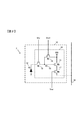
- FIG. 2 is a circuit diagram showing a configuration of the pixel 10 according to the first embodiment.
- the image sensor 3 has a plurality of pixels 10 arranged in a two-dimensional manner.
- the pixel 10 includes a photoelectric conversion unit 12 such as a photodiode (PD) and a reading unit 20.
- the photoelectric conversion unit 12 has a function of converting incident light into charges and accumulating the photoelectrically converted charges.
- the reading unit 20 includes a transfer unit 13, a discharge unit 14, a floating diffusion (FD) 15, an amplification unit 16, and a selection unit 17.
- FD floating diffusion
- the transfer unit 13 is controlled by the signal Vtx and transfers the electric charge photoelectrically converted by the photoelectric conversion unit 12 to the floating diffusion 15. That is, the transfer unit 13 forms a charge transfer path between the photoelectric conversion unit 12 and the floating diffusion 15.
- the floating diffusion 15 holds (accumulates) electric charges.
- the amplifying unit 16 amplifies the signal based on the charge held in the floating diffusion 15 and outputs the amplified signal to the vertical signal line 30 via the selection unit 17.
- the amplifying unit 16 includes a transistor M3 whose drain terminal, gate terminal, and source terminal are connected to the power supply VDD, the floating diffusion 15, and the selection unit 17, respectively.
- the source terminal of the amplifying unit 16 is connected to the vertical signal line 30 via the selecting unit 17.
- the amplifying unit 16 functions as a part of a source follower circuit using a current source 60 described later as a load current source.
- the discharge unit (reset unit) 14 is controlled by the signal Vrst, discharges the charge of the floating diffusion 15, and resets the potential of the floating diffusion 15 to the reset potential (reference potential).
- the selection unit 17 is controlled by the signal Vsel and outputs the signal from the amplification unit 16 to the vertical signal line 30.
- the transfer unit 13, the discharge unit 14, and the selection unit 17 are configured by, for example, a transistor M1, a transistor M2, and a transistor M4, respectively.
- the reading unit 20 receives a signal (photoelectric conversion signal) corresponding to the charge transferred from the photoelectric conversion unit 12 to the floating diffusion 15 by the transfer unit 13 and a signal (noise signal) when the potential of the floating diffusion 15 is reset to the reset potential. ) To the vertical signal line 30.
- the noise signal is a reference signal indicating a reference level for the photoelectric conversion signal.
- the amplification unit 16 and the selection unit 17 constitute an output unit that outputs a signal based on the electric charge accumulated in the floating diffusion 15, and the output unit outputs a photoelectric conversion signal and a noise signal to the vertical signal line 30.
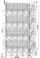
- FIG. 3 is a circuit diagram showing a configuration of a part of the image sensor 3 according to the first embodiment.
- the image pickup device 3 includes a plurality of pixels 10 arranged in a matrix, a vertical scanning circuit 40, a selection circuit 50, a current source 60 (current source 60a to current source 60d), and a first switch unit 70 (first switch).
- Switch unit 70a to first switch unit 70d second switch unit 80 (second switch unit 80a to second switch unit 80d), storage unit 90 (storage unit 90a to storage unit 90d), and horizontal scanning circuit 100
- FIG. 3 is a circuit diagram, and the storage unit 90 is drawn side by side with the pixels 10 for easy understanding.
- the pixels 10 are stacked on a semiconductor substrate in a pixel region in which the pixels 10 are densely arranged in a matrix.
- the storage unit 90 is arranged.
- the pixel region is a region in which a plurality of pixels 10 each having the photoelectric conversion unit 12 and the reading unit 20 are arranged two-dimensionally. That is, in the pixel region, a plurality of pixels 10 are arranged in a first direction (for example, the column direction) and a second direction (for example, the row direction) intersecting with the first direction (for example, the column direction).
- Peripheral circuits (such as the vertical scanning circuit 40 and the horizontal scanning circuit 100) are disposed outside the pixel region.
- a storage unit 90a is provided in the pixel region in which the first pixel column at the left end is arranged, and a storage unit 90b is provided in the pixel region in which the second pixel column on the right is arranged. .
- a storage unit 90c and a storage unit 90d are provided corresponding to the third pixel column and the fourth pixel column on the right side, respectively.
- the accumulation unit 90 is provided by being stacked on a semiconductor substrate in the pixel region.
- the accumulation unit 90 is arranged in parallel with the pixel 10 in the direction in which the accumulation unit 90 is stacked on the semiconductor substrate. For this reason, a large capacitance value can be obtained without increasing the chip area.
- a storage unit 90, a current source 60, a first switch unit 70, and a second switch unit 80 are provided for each pixel column including a plurality of pixels 10 arranged in the column direction, that is, in the vertical direction. That is, in FIG. 3, a storage unit 90, a current source 60, a first switch unit 70, and a second switch unit 80 are provided corresponding to the first pixel column at the left end. Corresponding to the second pixel column, corresponding to the right third pixel column, corresponding to the right fourth pixel column, the storage unit 90, A current source 60, a first switch unit 70, and a second switch unit 80 are provided.
- a vertical signal line 30 (vertical signal line 30a to vertical signal line 30d) is provided corresponding to each column of the pixels 10.
- a vertical signal line 30 vertical signal line 30a to vertical signal line 30d
- pixel in the horizontal direction 4 pixels ⁇ the pixel in the vertical direction 4 is illustrated in order to simplify the description.
- the current sources 60a to 60d are provided corresponding to the vertical signal lines 30a to 30d, respectively, and are connected to the vertical signal lines 30a to 30d.
- the current sources 60a to 60d are connected to the pixels 10 via the vertical signal lines 30a to 30d, respectively.
- the current sources 60a to 60d generate currents for reading out photoelectric conversion signals and noise signals from the respective pixels 10.
- the current sources 60a to 60d supply the generated currents to the vertical signal lines 30a to 30d and each pixel 10, respectively.
- the vertical scanning circuit 40 supplies control signals such as the signal Vtxn, the signal Vrstn, and the signal Vseln to each pixel 10.
- the vertical scanning circuit 40 outputs a signal Vtxn or the like to each pixel 10 to control the operation of each pixel 10.
- n at the end of Vtxn, Vrstn, and Vseln indicates the row number of the pixel.
- the signal Vtx1 is a signal that controls the transfer unit 13 of the pixels 10 in the first row.
- the first switch unit 70a to the first switch unit 70d are provided corresponding to the vertical signal line 30a to the vertical signal line 30d, respectively, and are connected to the vertical signal line 30a to the vertical signal line 30d.
- the first switch unit 70a to the first switch unit 70d switch the electrical connection state between the vertical signal line 30a to the vertical signal line 30d and the storage unit 90a to the storage unit 90d.
- the first switch unit 70a to the first switch unit 70d are controlled by the control signal output from the selection circuit 50, and the photoelectric conversion signal and the noise signal output from each pixel 10 are respectively stored in the storage units 90a to 90d. Forward.
- Each of the first switch unit 70a to the first switch unit 70d includes a switch TN1, a switch TS1, a switch TN2, and a switch TS2.
- the switch TN1, the switch TS1, the switch TN2, and the switch TS2 are each configured by a transistor.
- the second switch unit 80a to the second switch unit 80d are provided corresponding to the vertical signal line 30a to the vertical signal line 30d, respectively.
- the second switch unit 80a to the second switch unit 80d switch the electrical connection state between the storage units 90a to 90d and the output amplifier unit 110.
- the second switch unit 80a to the second switch unit 80d are controlled by a control signal output from the horizontal scanning circuit 100, and convert the photoelectric conversion signals and noise signals stored in the storage units 90a to 90d into the horizontal signal line S. Then, the data is transferred to the output amplifier unit 110 via the horizontal signal line N.
- Each of the second switch unit 80a to the second switch unit 80d includes a switch PH1N, a switch PH1S, a switch PH2N, and a switch PH2S.
- Switch PH1N, switch PH1S, switch PH2N, and switch PH2S are each configured by a transistor.
- the selection circuit 50 supplies control signals such as the signal Vtn1, the signal Vts1, the signal Vtn2, and the signal Vts2 to the first switch unit 70a to the first switch unit 70d.
- the selection circuit 50 outputs a control signal to control the operations of the first switch unit 70a to the first switch unit 70d.
- the horizontal scanning circuit 100 supplies control signals such as the signal Vph11, the signal Vph12, the signal Vph21, the signal Vph22, the signal Vph31, the signal Vph32, the signal Vph41, and the signal Vph42 to the second switch unit 80a to the second switch unit 80d.
- the horizontal scanning circuit 100 outputs a control signal to control operations of the second switch unit 80a to the second switch unit 80d.
- the accumulation units 90a to 90d are provided corresponding to the columns of the pixels 10 and accumulate (store) photoelectric conversion signals and noise signals output from the pixels 10.
- the accumulating units 90a to 90d have a capacity for accumulating photoelectric conversion signals and noise signals.
- the capacity is, for example, a capacity due to a conductor, such as a capacity formed by adjacent metals. Specifically, for example, the capacitance is formed between a conductor to which a photoelectric conversion signal or a noise signal is input and a conductor to which a predetermined potential is applied.
- each of the storage units 90a to 90d has conductors CN1 and CN2 to which noise signals are input, and conductors CS1 and CS2 to which photoelectric conversion signals are input. Further, each of the storage units 90a to 90d has a fixed potential line 120 as a conductor to which the above-described predetermined potential is applied. In FIG. 3, the fixed potential line 120 is indicated by a dotted line in order to distinguish it from the conductor CN1, the conductor CS1, the conductor CN2, and the conductor CS2.
- a symbol C indicating a plurality of capacitances shown in FIG. 3 is between the conductor CN1 and the fixed potential line 120, between the conductor CS1 and the fixed potential line 120, between the conductor CN2 and the fixed potential line 120, and between the conductor CS2 and This schematically shows that capacitors are formed between the fixed potential line 120 and each other.
- the conductors CN1 and CN2 function as a noise accumulation unit that accumulates noise signals
- the conductors CS1 and CS2 function as a signal accumulation unit that accumulates photoelectric conversion signals.
- the output amplifier unit 110 outputs a signal based on the difference between the noise signal input via the horizontal signal line N and the photoelectric conversion signal input via the horizontal signal line S to the output terminal shown in FIG. For example, the output amplifier unit 110 outputs a signal obtained by amplifying the difference between the noise signal and the photoelectric conversion signal with a predetermined gain.
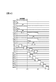
- FIG. 4 is a timing chart showing an operation example of the image sensor 3 according to the first embodiment.
- the vertical axis represents the voltage level of the control signal
- the horizontal axis represents time.
- a control signal when a control signal is at a high level (for example, a power supply potential), the transistor to which the control signal is input is turned on, and when the control signal is at a low level (for example, a ground potential), the control signal is input.
- the transistor to be turned off is turned off.
- Each of time t1 to time t10, time t10 to time t22, time t22 to time t34, time t34 to time t46, and time t46 to time t50 is one horizontal period.
- the charge accumulated in the photoelectric conversion unit 12 is reset in synchronization with the discharge of the floating diffusion 15, that is, the reset of the floating diffusion 15.
- a description of resetting the photoelectric conversion unit 12 is omitted.
- the signal Vsel1 becomes a high level, whereby the transistor M4 of the selection unit 17 is turned on in each pixel 10 in the first row.
- the signal Vrst1 becomes high level, so that the transistor M2 of the discharge unit 14 is turned on in each pixel 10 in the first row.
- the potential of the floating diffusion 15 becomes the reset potential.
- the noise signal of each pixel 10 in the first row is output to the vertical signal line 30a to the vertical signal line 30d by the amplification unit 16 and the selection unit 17, respectively.
- the signal Vrst1 becomes low level, so that the transistor M2 is turned off.
- the signal Vtn1 becomes a high level, so that the switches TN1 of the first switch unit 70a to the first switch unit 70d are turned on. As a result, the noise signal from each pixel 10 is transferred to the conductor CN1 of the storage units 90a to 90d.
- the capacitors added to the conductors CN1 of the storage units 90a to 90d store noise signals from the respective pixels 10 in the first row.
- the signal Vtn1 becomes low level, so that the switch TN1 is turned off. When the switch TN1 is turned off, the capacitor added to the conductor CN1 holds (accumulates) the noise signal.
- the transistor M1 of the transfer unit 13 is turned on in each pixel 10 in the first row. Thereby, the electric charge photoelectrically converted by the photoelectric conversion unit 12 is transferred to the floating diffusion 15. Further, the photoelectric conversion signal of each pixel 10 in the first row is output to the vertical signal line 30a to the vertical signal line 30d by the amplification unit 16 and the selection unit 17. At time t7, the signal Vtx1 becomes low level, so that the transistor M1 is turned off. At time t8, since the signal Vts1 becomes high level, the switches TS1 of the first switch unit 70a to the first switch unit 70d are turned on.
- the photoelectric conversion signal is transferred to the conductor CS1 of the storage units 90a to 90d.
- the capacitance added to the conductor CS1 accumulates photoelectric conversion signals from the pixels 10 in the first row.
- the signal Vts1 becomes low level, so that the switch TS1 is turned off.
- the capacitor added to the conductor CS1 holds the photoelectric conversion signal.
- the signal Vph11 and the signal Vsel2 become high level.
- the switch PH1N and the switch PH1S of the second switch unit 80a are turned on.
- signals from the pixels 10 in the first row accumulated in the accumulation unit 90a corresponding to the first column of each pixel 10 are output to the horizontal signal line S and the horizontal signal line N. That is, the photoelectric conversion signal stored in the conductor CS1 of the storage unit 90a is output to the horizontal signal line S, and the noise signal stored in the conductor CN1 of the storage unit 90a is output to the horizontal signal line N.
- the output amplifier unit 110 outputs a signal based on the difference between the noise signal and the photoelectric conversion signal.
- the transistor M4 of each pixel 10 in the second row is turned on.
- the signal Vrst2 becomes high level, so that the transistor M2 is turned on and the floating diffusion 15 is reset.
- the noise signal of each pixel 10 in the second row is output to the vertical signal line 30a to the vertical signal line 30d.
- the signal Vrst2 becomes low level, and the transistor M2 is turned off.
- the signal Vtn2 becomes high level, so that the switch TN2 is turned on.
- the noise signal is transferred to the conductor CN2 of the storage units 90a to 90d.
- the capacitance added to the conductor CN2 accumulates a noise signal from each pixel 10 in the second row.
- the signal Vph11 becomes low level and the signal Vph21 becomes high level.
- the switch PH1N and the switch PH1S of the second switch unit 80a are turned off.
- the switch PH1N and the switch PH1S of the second switch unit 80b are turned on.
- the photoelectric conversion signal from the pixel 10 in the first row accumulated in the accumulation unit 90b corresponding to the second column of each pixel 10 is output to the horizontal signal line S, and the noise signal is output to the horizontal signal line N. Is done.
- the output amplifier unit 110 outputs a signal based on the difference between the noise signal and the photoelectric conversion signal.
- the signal Vtn2 becomes low level, so that the switch TN2 is turned off.
- the capacitance added to the conductor CN2 holds the noise signal.
- the signal Vph21 becomes low level and the signal Vph31 becomes high level.
- the switch PH1N and the switch PH1S of the second switch unit 80b are turned off.
- the switch PH1N and the switch PH1S of the second switch unit 80c are turned on.
- the photoelectric conversion signal from the pixel 10 in the first row accumulated in the accumulation unit 90c corresponding to the third column of each pixel 10 is output to the horizontal signal line S, and the noise signal is output to the horizontal signal line N. Is done.
- the output amplifier unit 110 outputs a signal based on the difference between the noise signal and the photoelectric conversion signal.
- the signal Vtx2 becomes high level, so that the transistor M1 is turned on in each pixel 10 in the second row. Thereby, the electric charge photoelectrically converted by the photoelectric conversion unit 12 is transferred to the floating diffusion 15. Further, the photoelectric conversion signal of each pixel 10 in the second row is output to the vertical signal line 30a to the vertical signal line 30d. At time t18, the signal Vtx2 becomes low level, so that the transistor M1 is turned off. At time t19, since the signal Vts2 becomes high level, the switches TS2 of the first switch unit 70a to the first switch unit 70d are turned on. As a result, the photoelectric conversion signal is transferred to the conductor CS2 of the storage units 90a to 90d. The capacitance added to the conductor CS2 accumulates photoelectric conversion signals from the pixels 10 in the second row.
- the signal Vph31 becomes low level and the signal Vph41 becomes high level.
- the switch PH1N and the switch PH1S of the second switch unit 80c are turned off.
- the switch PH1N and the switch PH1S of the second switch unit 80d are turned on.
- the photoelectric conversion signal from the pixel 10 in the first row accumulated in the accumulation unit 90d corresponding to the fourth column of each pixel 10 is output to the horizontal signal line S, and the noise signal is output to the horizontal signal line N. Is done.
- the output amplifier unit 110 outputs a signal based on the difference between the noise signal and the photoelectric conversion signal.
- the signal Vts2 becomes low level, so that the switch TS2 is turned off.
- the capacitor added to the conductor CS2 holds the photoelectric conversion signal.
- the signals from the pixels 10 in the first row accumulated in the storage unit 90 are read out from the pixels 10 in the second row to the storage unit 90. Is transferred to the horizontal signal line S and the horizontal signal line N.
- the signal Vph41 becomes low level, and the signal Vph12 and the signal Vsel3 become high level.
- the switch PH1N and the switch PH1S of the second switch unit 80d are turned off.
- the switch PH2N and the switch PH2S of the second switch unit 80a are turned on.
- signals from the pixels 10 in the second row accumulated in the accumulation unit 90 a corresponding to the first column of the pixels 10 are output to the horizontal signal line S and the horizontal signal line N.
- the photoelectric conversion signal stored in the conductor CS2 of the storage unit 90a is output to the horizontal signal line S
- the noise signal stored in the conductor CN2 of the storage unit 90a is output to the horizontal signal line N.
- the output amplifier unit 110 outputs a signal based on the difference between the noise signal and the photoelectric conversion signal.
- the transistor M4 of each pixel 10 in the third row is turned on.
- the signal Vrst3 becomes high level, so that the transistor M2 is turned on and the floating diffusion 15 is reset.
- the noise signal of each pixel 10 in the third row is output to the vertical signal line 30a to the vertical signal line 30d.
- the signal Vrst3 becomes low level, and the transistor M2 is turned off.
- the signal Vtn1 becomes high level, so that the switch TN1 is turned on.
- the noise signal is transferred to the conductor CN1 of the storage units 90a to 90d.
- the capacitance added to the conductor CN1 accumulates a noise signal from each pixel 10 in the third row.
- the signal Vph12 becomes low level and the signal Vph22 becomes high level.
- the switch PH2N and the switch PH2S of the second switch unit 80a are turned off.
- the switch PH2N and the switch PH2S of the second switch unit 80b are turned on.
- the photoelectric conversion signal from each pixel 10 in the second row accumulated in the accumulation unit 90b corresponding to the second column of each pixel 10 is output to the horizontal signal line S, and the noise signal is applied to the horizontal signal line N. Is output.
- the output amplifier unit 110 outputs a signal based on the difference between the noise signal and the photoelectric conversion signal.
- the signal Vtn1 becomes low level, so that the switch TN1 is turned off.
- the capacitor added to the conductor CN1 holds the noise signal.
- the signal Vph22 becomes low level and the signal Vph32 becomes high level.
- the switch PH2N and the switch PH2S of the second switch unit 80b are turned off.
- the switch PH2N and the switch PH2S of the second switch unit 80c are turned on.
- the photoelectric conversion signal from each pixel 10 in the second row accumulated in the accumulation unit 90c corresponding to the third column of each pixel 10 is output to the horizontal signal line S, and the noise signal is output to the horizontal signal line N. Is output.
- the output amplifier unit 110 outputs a signal based on the difference between the noise signal and the photoelectric conversion signal.
- the signal Vtx3 becomes high level, so that the transistor M1 is turned on in each pixel 10 in the third row. Thereby, the electric charge photoelectrically converted by the photoelectric conversion unit 12 is transferred to the floating diffusion 15. Further, the photoelectric conversion signal of each pixel 10 in the third row is output to the vertical signal line 30a to the vertical signal line 30d. At time t30, the signal Vtx3 becomes low level, so that the transistor M1 is turned off. At time t31, since the signal Vts1 becomes high level, the switches TS1 of the first switch unit 70a to the first switch unit 70d are turned on. As a result, the photoelectric conversion signal is transferred to the conductor CS1 of the storage units 90a to 90d. The capacitance added to the conductor CS1 accumulates photoelectric conversion signals from the pixels 10 in the third row.
- the signal Vph32 becomes low level and the signal Vph42 becomes high level.
- the switch PH2N and the switch PH2S of the second switch unit 80c are turned off.
- the switch PH2N and the switch PH2S of the second switch unit 80d are turned on.
- the output amplifier unit 110 outputs a signal based on the difference between the noise signal and the photoelectric conversion signal.
- the switch TS1 is turned off.
- the capacitor added to the conductor CS1 holds the photoelectric conversion signal.
- the transistors controlled by the signals Vsel4, Vrst4, Vtn2, Vtx4, and Vts2 are sequentially turned on and off in the same manner as in the period from time t10 to time 22 and from time t22 to time 34.
- the noise signal from each pixel 10 in the fourth row is accumulated in the capacitor added to the conductor CN2, and the photoelectric conversion signal from each pixel 10 in the fourth row is accumulated in the capacitor added to the conductor CS2.
- the transistors controlled by the signals Vph11, Vph21, Vph31, and Vph41 are sequentially turned on and off.
- the noise signal and the photoelectric conversion signal from each pixel 10 in the third row stored in the storage units 90a to 90d are sequentially output.
- the output amplifier unit 110 sequentially outputs signals based on the difference between the noise signal output from the storage units 90a to 90d and the photoelectric conversion signal.
- the transistors controlled by the signals Vph12, Vph22, Vph32, and Vph42 are sequentially turned on and off.
- the noise signal and the photoelectric conversion signal from each pixel 10 in the fourth row respectively stored in the storage units 90a to 90d are sequentially output.
- the output amplifier unit 110 sequentially outputs signals based on the difference between the noise signal output from the storage units 90a to 90d and the photoelectric conversion signal.
- the signals from the pixels 10 in a certain row to the storage unit 90 are transmitted to the horizontal signal line S.
- the horizontal transfer to the horizontal signal line N is performed.
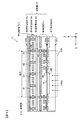
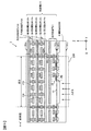
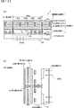
- FIG. 5 is a diagram illustrating an example of a cross-sectional structure of the image sensor 3 according to the first embodiment.
- FIG. 5 is a cross-sectional view taken along the line A-A ′ in FIG. 6 to be described later.
- the imaging device 3 is, for example, a backside illumination type imaging device.
- the incident light is incident mainly in the positive direction of the Z axis.
- the left direction on the paper orthogonal to the Z axis is defined as the X axis plus direction
- the back direction on the paper orthogonal to the Z axis and the X axis is defined as the Y axis plus direction.
- the coordinate axes are displayed so that the orientation of each figure can be understood with reference to the coordinate axes in FIG.
- the imaging device 3 includes a semiconductor substrate 200 made of a semiconductor material such as silicon and a wiring layer 210 stacked on the semiconductor substrate 200.
- the image sensor 3 further includes a microlens layer, a color filter layer, and a passivation layer (not shown).
- the imaging element 3 is arranged in the order of the microlens layer, the color filter layer, the passivation layer, the semiconductor substrate 200, and the wiring layer 210 in the positive direction of the Z axis.
- the semiconductor substrate 200 has a first surface 201a serving as an incident surface on which light is incident, and a second surface 201b different from the first surface 201a.
- the second surface 201b is positioned opposite to the first surface 201a.
- the back surface of the imaging device 3 shows the first surface 201a located on the opposite side to the wiring layer 210, and the back-illuminated type is configured such that light enters from the first surface 201a serving as the back surface.
- the wiring layer 210 has a surface (third surface 203a) on the second surface 201b side of the semiconductor substrate 200 and a surface opposite to the third surface 203a (fourth surface 203b).
- the semiconductor substrate 200 includes the photoelectric conversion unit 12 and the reading unit 20 between the first surface 201a and the second surface 201b.
- a plurality of pixels 10 each including the photoelectric conversion unit 12 and the reading unit 20 are arranged in the X-axis direction and the Y-axis direction.
- the photoelectric conversion unit 12 converts incident light incident from one side of the semiconductor substrate 200, that is, the first surface 201 a side of the semiconductor substrate 200 into electric charge.
- the accumulation unit 90 is provided so as to be stacked with the photoelectric conversion unit 12 on the side opposite to one side of the semiconductor substrate 200, that is, on the second surface 201 b side of the semiconductor substrate 200.
- the storage unit 90 is provided between the photoelectric conversion unit 12 and the fourth surface 203 b of the wiring layer 210.
- a multilayer wiring layer 210 including a conductor film (metal film) and an insulating film is formed on the second surface 201b of the semiconductor substrate 200.
- a plurality of wirings and vias are arranged. Copper, aluminum, or the like is used for the conductor film.
- the insulating film includes an insulating film between the conductor films, a gate insulating film, and the like, and is configured by an oxide film, a nitride film, or the like.
- the wiring layer 210 includes a signal wiring layer 211 provided with signal lines such as control signals Vtxn, Vrstn, and Vseln input to each pixel 10 and a vertical signal line 30, and an accumulation unit 90 (accumulation units 90a to 90d). And an accumulating portion wiring layer 212.
- the signal wiring layer 211 is stacked on the second surface 201b of the semiconductor substrate 200, and the storage unit wiring layer 212 is stacked on the signal wiring layer 211a.
- the storage unit wiring layer 212 is formed by stacking the storage unit 90 a corresponding to the first pixel column via the signal wiring layer 211 in the pixel region where the first pixel column is located. Then, in the pixel region where the second pixel row is located, a storage unit 90b corresponding to the second pixel row is stacked via the signal wiring layer 211, and similarly, the pixels in the third row are stacked. Storage units 90 c and 90 d corresponding to the column and the fourth pixel column are stacked via the signal wiring layer 211. In this way, each of the storage units 90a to 90d of the storage unit wiring layer 212 is provided in each pixel region 220 for each corresponding pixel column.
- Each of the storage portions 90a to 90d of the storage portion wiring layer 212 has a size corresponding to the pixels 10 for one column.
- the storage units 90a to 90d of the storage unit wiring layer 212 have the same configuration, and the storage unit 90 shown in FIG. 5 corresponds to any one of the storage units 90a to 90d.
- the storage unit 90 includes the conductor CN1, the conductor CS1, the conductor CN2, the conductor CS2, and the fixed potential line 120 as described above.
- the fixed potential line 120 includes a first fixed potential line 120 a, a second fixed potential line 120 b, and a third fixed potential line 120 c, each of which is constituted by a conductor film of a different layer.
- the first fixed potential line 120 a and the third fixed potential line 120 c are arranged apart from each other in the Z-axis direction, which is the stacking direction of the wiring layers 210.
- the first fixed potential line 120a and the third fixed potential line 120c are common to all the accumulation units 90a, 90b, 90c, and 90d, and are thus formed so as to cover all the pixels 10 of the image sensor 3.
- the first fixed potential line 120a and the third fixed potential line 120c may be configured in common for all the storage units as described above, or may be configured for each storage unit.
- the conductor CN1, the conductor CS1, the conductor CN2, and the conductor CS2 extend in the arrangement direction of the plurality of pixels 10 constituting each pixel column.
- the conductors CN1, CS1, CN2, and CS2 are disposed between the first fixed potential line 120a and the third fixed potential line 120c and separated from the first fixed potential line 120a and the third fixed potential line 120c.
- the second fixed potential line 120b is disposed between each of the conductors CN1, CS1, CN2, and CS2, and is connected to the first fixed potential line 120a and the third fixed potential line 120c through vias.
- An insulating film is provided between the conductors CN1, CS1, CN2, and CS2 and the first to third fixed potential lines 120a to 120c.
- the insulating film is an oxide film or a nitride film. Specifically, a silicon oxide film, a silicon nitride film, a silicon oxynitride film, or a multilayer film
- capacitance is formed between each of the conductors CN1, CS1, CN2, and CS2 and the first to third fixed potential lines 120a to 120c.
- the capacitance can be increased.
- a high dielectric material having a dielectric constant higher than that of a silicon oxide film or the like may be used.
- an MIM capacity may be used. Note that a capacitance formed between the conductors CN1, CS1, CN2, and CS2 and a wiring different from the fixed potential line is also added.
- the first fixed potential line 120a, the second fixed potential line 120b, and the third fixed potential line 120c are given a predetermined potential such as a power supply potential or a ground potential.
- the first fixed potential line 120a functions as a shield between the vertical signal line 30 and the control signal line of the signal wiring layer 211 and the conductors CN1, CS1, CN2, and CS2.
- By providing the first fixed potential line 120a it is possible to suppress the formation of a large parasitic capacitance between the vertical signal line 30, the control signal line, and the like and the conductors CN1, CS1, CN2, and CS2. Further, crosstalk between the vertical signal line 30, the control signal line, and the like and the conductors CN1, CS1, CN2, and CS2 can be suppressed.
- the first fixed potential line 120a, the second fixed potential line 120b, and the third fixed potential line 120c are provided so as to surround each of the conductors CN1, CS1, CN2, and CS2, so that the conductors CN1, CS1 , CN2 and CS2 function as a shield.
- a large parasitic capacitance can be avoided between the conductors CN1, CS1, CN2, and CS2, and crosstalk between the conductors CN1, CS1, CN2, and CS2 can be suppressed.
- the first fixed potential line 120a is set to the ground potential and is connected to the semiconductor substrate 200 via the via 202 or the like.
- the first fixed potential line 120 a is commonly connected to each pixel 10 as a ground line (ground line) for supplying a ground potential to each pixel 10.
- a power supply potential may be applied to the first fixed potential line 120a so that the pixel 10 is used as a common power supply line.
- the fixed potential line is shared by the conductors for forming the capacitances of the conductors CN1, CS1, CN2, and CS2, the shield for suppressing the mixing of noise, and the power supply line or the ground line of each pixel 10. .
- the fixed potential line By using the fixed potential line as a power supply line or a ground line for each pixel 10, it is not necessary to separately provide a wiring for the power supply line or the ground line. For this reason, the number of wiring layers 210 can be reduced.
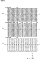
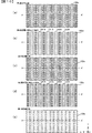
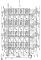
- FIG. 6 is a diagram illustrating an example of a planar layout of a part of the storage unit wiring layer 212 of the image sensor 3 according to the first embodiment.
- FIG. 6A shows an example of a planar layout of a layer in which the third fixed potential line 120c is formed
- FIG. 6B shows the second fixed potential line 120b and conductors CN1, CS1, CN2, and CS2.
- FIG. 6C is a diagram illustrating an example of a planar layout of a layer on which the first fixed potential line 120a is formed.
- the third fixed potential line 120c and the first fixed potential line 120a are formed in a planar shape as shown in FIG.
- the third fixed potential line 120c and the first fixed potential line 120a are formed so as to cover all the pixels 10 that are two-dimensionally arranged in a matrix, for example.
- the second fixed potential line 120b, the conductor CN1, the conductor CS1, the conductor CN2, and the conductor CS2 are each formed in a linear shape.
- the second fixed potential line 120b is disposed to face the conductors CN1, CS1, CN2, and CS2.
- the length of the second fixed potential line 120b in the Y-axis direction is a length corresponding to the length of the conductors CN1, CS1, CN2, and CS2 in the Y-axis direction.
- the storage units 90a to 90d are provided corresponding to the pixel columns of the respective pixels 10, the lengths of the second fixed potential line 120b and the conductors CN1, CS1, CN2, and CS2 in the Y-axis direction The length corresponds to one pixel column.
- the third fixed potential line 120c and the second fixed potential line 120b are connected via a plurality of vias, and the second fixed potential line 120b and the first fixed potential line 120a are connected via a plurality of vias.
- the imaging device 3 includes a photoelectric conversion unit 12 that converts incident light incident from one side of the substrate 200 into charges, and an output unit (amplification unit 16 and selection unit 17) that outputs a signal based on charges.
- the plurality of pixels 10 arranged in the first direction and the second direction intersecting the first direction are stacked with the photoelectric conversion unit 12 on the side opposite to the one side of the substrate 200 to accumulate signals.
- an accumulation unit 90 is provided by being stacked on the second surface 201 b of the semiconductor substrate 200 in the pixel region 220.
- the chip area of the image sensor is increased by providing a large number of capacitors in a region where an analog / digital conversion circuit and the like around the pixel region 220 are arranged.
- the accumulation unit 90 is provided by being stacked on the second surface 201b of the semiconductor substrate 200. For this reason, an increase in chip area can be suppressed.
- the storage unit 90 in the pixel region 220, it is possible to avoid an increase in the area of the region where the analog / digital conversion circuit and the like around the pixel region 220 are arranged.
- a large capacity can be formed by providing a capacity corresponding to one pixel column or the like.
- the imaging device 3 includes a photoelectric conversion unit 12 that converts light incident on the first surface 201a of the semiconductor substrate 200 into charges, and a readout unit 20 that outputs a signal due to charges on the second surface 201b of the semiconductor substrate 200.
- a storage unit 90 that is stacked on the pixel region 220 of the second surface 201b and stores the signal output from the readout unit 20. Since it did in this way, the increase in a chip area can be suppressed.
- the storage unit 90 is commonly connected to the plurality of pixels 10 arranged in the first direction. Since it did in this way, a capacity
- the imaging device 3 further includes a signal line (vertical signal line 30) that is connected in common to the plurality of pixels 10 arranged in the first direction and that outputs a signal from the readout unit 20.
- the storage unit 90 is commonly connected to the plurality of pixels 10 via signal lines. Since it did in this way, the signal from each pixel 10 read via the vertical signal line 30 can be stored in the storage unit 90.
- the reading unit 20 outputs a signal based on charges and a noise signal.
- the accumulating unit 90 includes a signal accumulating unit that accumulates signals based on electric charges, and a noise accumulating unit that accumulates noise signals. Since it did in this way, the photoelectric conversion signal and noise signal which are output from the read-out part 20 can be accumulated in accumulation part 90, respectively.
- first wiring (second fixed potential line 120b) provided between the signal storage unit and the noise storage unit to which a constant potential (for example, a power supply potential or a ground potential) is applied;
- a second wiring (first fixed potential line 120a) provided between the storage unit 90 and a constant potential is applied to the side opposite to the light incident side, with the storage unit 90 and the insulating film interposed therebetween.
- a third wiring (third fixed potential line 120c) to which a constant potential is applied.
- the first fixed potential line 120a, the second fixed potential line 120b, and the third fixed potential line 120c are provided so as to surround each of the conductors CN1, CS1, CN2, and CS2. For this reason, mixing of noise can be suppressed.
- the storage unit 90 includes a first storage unit (for example, a storage unit 90a) connected to the plurality of pixels 10 arranged in the first direction, and a plurality of units arranged in the first direction different from the plurality of pixels 10.
- a second storage unit (for example, storage unit 90b) connected to the pixel, and a plurality of first storage units and second storage units are provided side by side in the second direction. Since it did in this way, the accumulation
- the reading unit 90 includes a holding unit 15 that holds the charge converted by the photoelectric conversion unit 12, a transfer unit 13 that transfers the charge to the holding unit 15, and a discharge that discharges the charge held by the holding unit 15. And an amplifying unit 16 that amplifies a signal based on the charges transferred by the transfer unit 13. Since it did in this way, the photoelectric conversion signal based on the electric charge photoelectrically converted by the photoelectric conversion part 12 from each pixel 10 can be read. (9)
- the noise signal is a signal when the electric charge held in the holding unit 15 is discharged. Since it did in this way, the noise signal used as the reference level with respect to a photoelectric conversion signal can be obtained.
- the imaging device 3 includes a photoelectric conversion unit 12 that converts light incident on the first surface 201a of the semiconductor substrate 200 into electric charge, and a reading unit 20 that outputs a signal based on electric charge to the second surface 201b of the semiconductor substrate 200. , And a second layer (storage portion wiring layer 212) that is stacked on the first layer on the second surface 201 b and has a storage portion 90 that stores the signal output by the reading portion 20. And). Since this is done, a large capacitance value can be obtained without increasing the chip area. (11)
- the storage unit 90 has a capacitance due to a conductor. Since it did in this way, increase of a chip area can be suppressed compared with the case where diffusion capacity is provided.
- the imaging device 3 includes a photoelectric conversion unit 12 that converts incident light into electric charges, a first accumulation unit (floating diffusion 15) to which electric charges converted by the photoelectric conversion unit 12 are transferred, and a first Pixels 10 having an output unit (amplifying unit 16 and selection unit 17) for outputting a signal based on the charge transferred to the storage unit, and a pixel based on the charge transferred from the photoelectric conversion unit 12 to the first storage unit
- An output control unit (vertical scanning circuit 40) that switches a signal (photoelectric conversion signal) and a reset signal (noise signal) that resets the charge of the first accumulation unit to output from the output unit, and is output from the output unit
- the pixel 10 is disposed between the light incident surface and the second accumulation unit or the third accumulation unit. Since it did in this way, the increase in a chip area can be suppressed
- the imaging device according to the second embodiment has a configuration similar to that of the imaging device 1 according to the first embodiment.
- the image sensor according to the second embodiment is different from the first embodiment mainly in that a plurality of vertical signal lines are provided for each pixel column to simultaneously read out the pixels 10 in a plurality of rows.
- the same or corresponding parts as those in the first embodiment are denoted by the same reference numerals, and differences will mainly be described.
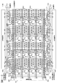
- FIG. 7 is a circuit diagram showing a partial configuration of the image sensor 3 according to the second embodiment.
- two vertical signal lines (vertical signal line 30 ⁇ / b> A and vertical signal line 30 ⁇ / b> B) are provided corresponding to each column of the pixels 10.
- the pixels 10 in each column are connected to different vertical signal lines for each row.
- the imaging device 3 includes a selection circuit 50 (selection circuit 50A and selection circuit 50B), and a current source 60 (current source 60A1 to current source 60A3, current source 60B1 to current source 60B3).
- the first switch unit 70 (first switch unit 70A1 to first switch unit 70A3, first switch unit 70B1 to first switch unit 70B3), and second switch unit 80 (second switch unit 80A1 to second switch unit 80A3) , Second switch unit 80B1 to second switch unit 80B3), storage unit 90 (storage unit 90A1 to storage unit 90A3, storage unit 90B1 to storage unit 90B3), and horizontal scanning circuit 100 (horizontal scanning circuit 100A and horizontal scanning circuit). 100B) and the output amplifier unit 110 (the output amplifier unit 110A and the output amplifier unit 110B).
- the pixel 10 shows only 3 pixels in the horizontal direction ⁇ 4 pixels in the vertical direction.
- FIG. 8 is a timing chart showing an operation example of the image sensor 3 according to the second embodiment.
- time t1 to time t10, time t10 to time t22, and time t22 to time t26 are each one horizontal period.
- the signal Vsel1 and the signal Vsel2 are at a high level, whereby the transistor M4 of the selection unit 17 is turned on in each pixel 10 in the first row and the second row.
- the signal Vrst1 and the signal Vrst2 are set to the high level, whereby the transistor M2 of the discharge unit 14 is turned on in each pixel 10 in the first and second rows, and the potential of the floating diffusion 15 is set to the reset potential.
- the noise signal of each pixel 10 in the first row is output to the vertical signal line 30B1 to the vertical signal line 30B3, respectively, and the noise signal of each pixel 10 in the second row is output to the vertical signal line 30A1 to the vertical signal line 30A3, respectively. Is done.
- the signal Vrst1 and the signal Vrst2 are at a low level, so that the transistor M2 is turned off.
- the signal Vtn1 becomes high level, so that the switches TN1 of the first switch unit 70A1 to the first switch unit 70A3 and the first switch unit 70B1 to the first switch unit 70B3 are turned on.
- the noise signal from each pixel 10 in the first row is transferred to the conductor CN1B of the storage unit 90B1 to storage unit 90B3
- the noise signal from each pixel 10 in the second row is transferred to the conductor of the storage unit 90A1 to storage unit 90A3. Transferred to CN1A.
- the signal Vtn1 becomes low level, so that the switch TN1 is turned off.
- the capacitors added to the conductors CN1B of the storage units 90B1 to 90B3 hold the noise signals from the respective pixels 10 in the first row. Further, the capacitors added to the conductors CN1A of the storage units 90A1 to 90A3 hold noise signals from the respective pixels 10 in the second row.
- the signal Vtx ⁇ b> 1 and the signal Vtx ⁇ b> 2 become high level, whereby the transistor M ⁇ b> 1 of the transfer unit 13 is turned on in each pixel 10 in the first row and second row, and the photoelectric conversion unit 12 performs photoelectric conversion.
- the charge is transferred to the floating diffusion 15.
- the photoelectric conversion signals of the pixels 10 in the first row are output to the vertical signal lines 30B1 to 30B3, respectively, and the photoelectric conversion signals of the pixels 10 in the second row are respectively the vertical signal lines 30A1 to 30A3. Is output.
- the signal Vtx1 and the signal Vtx2 are at a low level, so that the transistor M1 is turned off.
- the signal Vts1 becomes high level, so that the switches TS1 of the first switch unit 70A1 to the first switch unit 70A3 and the first switch unit 70B1 to the first switch unit 70B3 are turned on.
- the photoelectric conversion signals from the pixels 10 in the first row are transferred to the conductors CS1B of the storage units 90B1 to 90B3, and the photoelectric conversion signals from the pixels 10 in the second row are stored in the storage units 90A1 to 90A3. Is transferred to the conductor CS1A.
- the signal Vts1 becomes low level, so that the switch TS1 is turned off.
- the capacitors added to the conductors CS1B of the storage units 90B1 to 90B3 hold the photoelectric conversion signals from the respective pixels 10 in the first row.
- the capacitance added to the conductor CS1A of the storage units 90A1 to 90A3 holds the photoelectric conversion signal from each pixel 10 in the second row.
- the signals of the pixels 10 in the first row are read out to the storage units 90B1 to 90B3, and the signals of the pixels 10 in the second row are stored in the storage unit.
- 90A1 to 90A3 are read out.
- the transistors controlled by the signals Vsel3, Vsel4, Vrst3, Vrst4, Vtn2, Vtx3, Vtx4, and Vts2 are sequentially turned on and off as in the case of the period from time t1 to time 10.
- the noise signals and photoelectric conversion signals from the respective pixels 10 in the third row are accumulated in the capacitors added to the conductors CN2B and CS2B of the accumulation units 90B1 to 90B3, respectively.
- noise signals and photoelectric conversion signals from the respective pixels 10 in the fourth row are accumulated in the capacitors added to the conductors CN2A and CS2A of the accumulation units 90A1 to 90A3, respectively.
- the conductors CN1A, CN2A, CN1B, and CN2B function as a noise accumulation unit that accumulates noise signals.
- the conductors CS1A, CS2A, CS1B, and CS2B function as a signal storage unit that stores photoelectric conversion signals.
- the signal Vph11 becomes high level, so that the switches PH1N and PH1S of the second switch unit 80A1 and the second switch unit 80B1 are turned on.
- signals from the pixels 10 in the first row accumulated in the accumulation unit 90B1 are output to the horizontal signal line BS and the horizontal signal line BN.
- signals from the pixels 10 in the second row accumulated in the accumulation unit 90A1 are output to the horizontal signal line AS and the horizontal signal line AN.
- Each of the output amplifier unit 110A and the output amplifier unit 110B outputs a signal based on the difference between the noise signal and the photoelectric conversion signal.
- the transistors controlled by the signals Vph12, Vph22, and Vph32 are sequentially turned on and off.
- the noise signal and the photoelectric conversion signal from each pixel 10 in the third row stored in the storage units 90B1 to 90B3 are sequentially output.
- noise signals and photoelectric conversion signals from the respective pixels 10 in the fourth row stored in the storage units 90A1 to 90A3 are sequentially output.
- the output amplifier unit 110A and the output amplifier unit 110B sequentially output signals based on the difference between the noise signal and the photoelectric conversion signal.
- FIG. 9 is a diagram illustrating an example of a cross-sectional structure of the image sensor 3 according to the second embodiment.
- FIG. 9 is a cross-sectional view taken along line A-A ′ in FIG. 10 to be described later.
- the wiring layer 210 is provided with a storage part wiring layer 212A having a storage part 90A (storage part 90A1 to storage part 90A3) and a storage part wiring layer 212B having storage parts 90B (storage part 90B1 to storage part 90B3).
- the storage portion wiring layer 212B is provided so as to be stacked on the storage portion wiring layer 212A in the pixel region 220 of the second surface 201b of the semiconductor substrate 200.
- the sizes of the storage unit 90A and the storage unit 90B correspond to the pixels 10 for one column.
- the fixed potential line 120 includes a first fixed potential line 120a, a second fixed potential line 120b, a third fixed potential line 120c, a fourth fixed potential line 120d, and a fifth fixed potential line 120e.
- the conductive films are formed of different layers.
- capacitance is mainly formed between each of the conductors CN1A, CS1A, CN2A, CS2A and the first to third fixed potential lines 120a to 120c.
- a capacitor is formed mainly between each of the conductors CN1B, CS1B, CN2B, CS2B and the third to fifth fixed potential lines 120c to 120e.
- the third fixed potential line 120c functions as a shield between the conductors CN1A, CS1A, CN2A, CS2A of the storage unit 90A and the conductors CN1B, CS1B, CN2B, CS2B of the storage unit 90B.
- FIG. 10 is a diagram illustrating an example of a planar layout of a part of the storage unit wiring layer 212 of the image sensor 3 according to the second embodiment.
- FIG. 10A shows an example of a planar layout of a layer in which the fifth fixed potential line 120e is formed
- FIG. 10B shows the fourth fixed potential line 120d and the conductors CN1B, CS1B, CN2B, CS2B formed.
- FIG. 10C is a diagram showing an example of a planar layout of a layer on which the third fixed potential line 120c is formed.
- FIG. 10D is a diagram showing an example of a planar layout of the layer on which the second fixed potential line 120b and the conductors CN1A, CS1A, CN2A, and CS2A are formed.
- FIG. 10E shows the first fixed potential line 120a. It is a figure which shows an example of the planar layout of the layer formed.
- the fifth fixed potential line 120e is formed so as to cover all the pixels 10 that are two-dimensionally arranged in a matrix, for example.
- the fourth fixed potential line 120d is formed in a linear shape like the second fixed potential line 120b.
- the storage unit 90A and the storage unit 90B are provided corresponding to the pixel columns of the respective pixels 10, the length of the fourth fixed potential line 120d, the conductors CN1B, CS1B, CN2B, and CS2B in the Y-axis direction The length corresponds to one pixel column.
- the fifth fixed potential line 120e and the fourth fixed potential line 120d are connected via a plurality of vias, and the fourth fixed potential line 120d and the third fixed potential line 120c are connected via a plurality of vias.
- the accumulation unit 90 includes a first accumulation unit 90A connected to the first plurality of pixels 10 among the plurality of pixels 10 arranged in the first direction, and a plurality of pixels arranged in the first direction. 10 and a second storage unit 90 ⁇ / b> B connected to the second plurality of pixels 10.
- the imaging device 3 further includes a third layer (accumulation unit wiring layer 212B) stacked on the second layer (accumulation unit wiring layer 212A). Since it did in this way, while being able to suppress expansion of a chip area, the some storage part 90 can be provided. Further, by providing a plurality of accumulation units 90 for each pixel column, simultaneous reading of the pixels 10 in a plurality of rows can be realized.
- the imaging device according to the third embodiment has a configuration similar to that of the imaging device 1 according to the first embodiment.
- the imaging element according to the third embodiment is different from the second embodiment in that the storage unit 90A and the storage unit 90B are arranged without being stacked, respectively.
- the same or corresponding parts as those in the first and second embodiments are denoted by the same reference numerals, and different points will be mainly described.
- FIG. 11 is a circuit diagram showing a configuration of part of the image sensor 3 according to the third embodiment.
- the image sensor according to the third embodiment has a circuit configuration similar to that of the image sensor 3 according to the second embodiment.
- the second embodiment the example in which each of the storage unit 90A and the storage unit 90B is provided with a size corresponding to one column of pixels 10 has been described.
- each of the accumulation unit 90A and the accumulation unit 90B is provided in a size corresponding to a predetermined number of pixels 10 among the pixels 10 for one column.
- the sizes of the storage unit 90A and the storage unit 90B are the sizes corresponding to the pixels 10 in one column half.
- the operation of the image sensor 3 according to the third embodiment is the same as that of the image sensor 3 according to the second embodiment.
- FIG. 12 is a diagram illustrating an example of a cross-sectional structure of the image sensor 3 according to the third embodiment.
- 12A is a cross-sectional view taken along the line A-A ′ in FIG. 13 described later
- FIG. 12B is a cross-sectional view taken along the line B-B ′ in FIG. 13 described later.
- the storage unit wiring layer 212 of the wiring layer 210 is provided with a storage unit 90A (storage unit 90A1 to storage unit 90A4) and a storage unit 90B (storage unit 90B1 to storage unit 90B4).
- the storage unit 90B is shown.
- the storage portion 90A and the storage portion 90B are formed using the same layer of conductor film or insulating film.
- FIG. 13 is a diagram illustrating an example of a planar layout of a part of the storage unit wiring layer 210 of the image sensor 3 according to the third embodiment.
- FIG. 13A is a diagram illustrating an example of a planar layout of a layer in which the third fixed potential line 120c is formed.
- FIG. 13B is a diagram illustrating the second fixed potential line 120b and the conductors CN1A, CS1A, CN2A, CS2A, CN1B
- FIG. 13C is a diagram showing an example of the planar layout of the layer in which CS1B, CN2B, CS2B is formed
- FIG. 13C is a diagram showing an example of the planar layout of the layer in which the first fixed potential line 120a is formed.
- the second fixed potential line 120b is disposed between each of the conductors CN1A, CS1A, CN2A, CS2A of the storage unit 90A.
- the second fixed potential line 120b is disposed between the conductors CN1B, CS1B, CN2B, CS2B of the storage unit 90B.
- each of the storage unit 90A and the storage unit 90B corresponds to a predetermined number of pixels 10 in one pixel column, so the conductors CN1A, CS1A, CN2A, CS2A, and the conductor CN1B , CS1B, CN2B, and CS2B in the Y-axis direction are lengths corresponding to a predetermined number of pixels 10 in one pixel column.
- the second fixed potential line 120b functions as a shield between the conductors CN1A, CS1A, CN2A, CS2A of the storage unit 90A and the conductors CN1B, CS1B, CN2B, CS2B of the storage unit 90B.
- the accumulation unit 90 includes a first accumulation unit 90A connected to the first plurality of pixels 10 among the plurality of pixels 10 arranged in the first direction, and a plurality of pixels arranged in the first direction. 10 and a second storage unit 90B connected to the second plurality of pixels.
- each of the plurality of accumulation units 90 corresponds to each of the plurality of pixel columns, and stores signals read from the pixels 10 of the corresponding pixel columns.
- the plurality of accumulation units 90 are provided in the pixel region 200 including a predetermined number of pixels in the corresponding pixel column. Since it did in this way, the some accumulation
- FIG. 14 is a circuit diagram illustrating a partial configuration of the image sensor 3 according to the first modification.
- the imaging device 3 according to the modification 1 includes an amplifier (buffer) 130 connected to each vertical signal line 30.
- the amplifier 130 (amplifiers 130a to 130d) outputs a signal obtained by amplifying the signal read from the pixel 10. For this reason, it is possible to suppress signal delay and signal level decrease between each pixel 10 and each storage unit 90. As a result, for example, even when the storage unit 90 has a large capacity, reading at a high frame rate can be performed.
- two analog / digital conversion circuits are provided for each pixel column.
- the AD conversion circuit 140A and the AD conversion circuit 140B each output a digital signal based on the difference between the photoelectric conversion signal and the noise signal from the corresponding pixel column.
- the digital signal output from the AD conversion circuit 140A and the digital signal output from the AD conversion circuit 140B are averaged.
- the digital signal output from the AD conversion circuit 140A1 and the digital signal output from the AD conversion circuit 140B1 are averaged, and the digital signal output from the AD conversion circuit 140A2 and the digital signal output from the AD conversion circuit 140B2 are obtained. Averaged.
- the digital signal output from the AD conversion circuit 140A3 and the digital signal output from the AD conversion circuit 140B3 are averaged, and the digital signal output from the AD conversion circuit 140A4 and the digital signal output from the AD conversion circuit 140B4 are averaged.
- the signal is averaged.
- the averaged signal is output to the output terminal shown in FIG.
- the signal from each pixel 10 accumulated in the accumulation unit 90 is converted into a digital signal by each of the AD conversion circuit 140A and the AD conversion circuit 140B, and the two digital signals are averaged. For this reason, it is possible to output to the output terminal a signal with reduced noise that is mixed when the signal is transferred from the storage unit 90 to the second switch unit 80.
- the example in which the signal wiring layer 211 is stacked on the second surface 201b of the semiconductor substrate 200 and the storage unit wiring layer 212 is stacked on the signal wiring layer 211 has been described.
- the storage unit wiring layer 212 may be stacked on the second surface 201 b of the semiconductor substrate 200, and the signal wiring layer 211 may be stacked on the storage unit wiring layer 212.
- the storage portion wiring layer 212 may be laminated on the second surface 201b of the semiconductor substrate 200 via a conductor film or an insulating film, or may be laminated directly.
- the imaging device 3 may have a surface irradiation type configuration in which the wiring layer 210 is provided on the incident surface on which light is incident.
- the imaging device 3 is configured such that light is incident on the second surface 201b of the semiconductor substrate 200.
- a plurality of pixels 10 are arranged in a first direction (for example, the column direction) and in a second direction (for example, the row direction) intersecting therewith.
- the accumulation unit 90 may be arranged between a plurality of pixels, for example, a plurality of pixels arranged in the second direction.
Landscapes
- Engineering & Computer Science (AREA)
- Multimedia (AREA)
- Signal Processing (AREA)
- Physics & Mathematics (AREA)
- Electromagnetism (AREA)
- Solid State Image Pick-Up Elements (AREA)
- Transforming Light Signals Into Electric Signals (AREA)
Priority Applications (6)
| Application Number | Priority Date | Filing Date | Title |
|---|---|---|---|
| US16/078,807 US10879300B2 (en) | 2016-02-29 | 2017-02-27 | Image sensor and image-capturing apparatus |
| EP17759935.4A EP3425902B1 (en) | 2016-02-29 | 2017-02-27 | Imaging element and imaging device |
| CN201780025799.1A CN109076180B (zh) | 2016-02-29 | 2017-02-27 | 摄像元件及摄像装置 |
| JP2018503304A JP7075881B2 (ja) | 2016-02-29 | 2017-02-27 | 撮像素子および撮像装置 |
| US17/100,177 US12199126B2 (en) | 2016-02-29 | 2020-11-20 | Image sensor and image-capturing apparatus |
| US18/976,649 US20250107254A1 (en) | 2016-02-29 | 2024-12-11 | Image sensor and image-capturing apparatus |
Applications Claiming Priority (2)
| Application Number | Priority Date | Filing Date | Title |
|---|---|---|---|
| JP2016038161 | 2016-02-29 | ||
| JP2016-038161 | 2016-02-29 |
Related Child Applications (2)
| Application Number | Title | Priority Date | Filing Date |
|---|---|---|---|
| US16/078,807 A-371-Of-International US10879300B2 (en) | 2016-02-29 | 2017-02-27 | Image sensor and image-capturing apparatus |
| US17/100,177 Continuation US12199126B2 (en) | 2016-02-29 | 2020-11-20 | Image sensor and image-capturing apparatus |
Publications (1)
| Publication Number | Publication Date |
|---|---|
| WO2017150469A1 true WO2017150469A1 (ja) | 2017-09-08 |
Family
ID=59742997
Family Applications (1)
| Application Number | Title | Priority Date | Filing Date |
|---|---|---|---|
| PCT/JP2017/007548 Ceased WO2017150469A1 (ja) | 2016-02-29 | 2017-02-27 | 撮像素子および撮像装置 |
Country Status (5)
| Country | Link |
|---|---|
| US (3) | US10879300B2 (enExample) |
| EP (1) | EP3425902B1 (enExample) |
| JP (2) | JP7075881B2 (enExample) |
| CN (2) | CN109076180B (enExample) |
| WO (1) | WO2017150469A1 (enExample) |
Citations (6)
| Publication number | Priority date | Publication date | Assignee | Title |
|---|---|---|---|---|
| JP2001045375A (ja) | 1999-08-03 | 2001-02-16 | Canon Inc | 撮像装置とその読み出し方法 |
| JP2005303621A (ja) * | 2004-04-09 | 2005-10-27 | Link Research Kk | 高速撮像装置 |
| JP2013126174A (ja) * | 2011-12-15 | 2013-06-24 | Canon Inc | 電子回路 |
| JP2014195112A (ja) * | 2005-06-02 | 2014-10-09 | Sony Corp | 半導体イメージセンサ・モジュール及びその製造方法 |
| JP2015228388A (ja) * | 2012-09-25 | 2015-12-17 | ソニー株式会社 | 固体撮像装置、電子機器 |
| WO2016009943A1 (ja) * | 2014-07-15 | 2016-01-21 | ブリルニクスジャパン株式会社 | 固体撮像装置、固体撮像装置の製造方法、および電子機器 |
Family Cites Families (23)
| Publication number | Priority date | Publication date | Assignee | Title |
|---|---|---|---|---|
| JP3874135B2 (ja) * | 1997-12-05 | 2007-01-31 | 株式会社ニコン | 固体撮像素子 |
| JP4809999B2 (ja) | 2001-05-25 | 2011-11-09 | キヤノン株式会社 | 放射線撮像装置及び放射線撮像システム |
| JP4724313B2 (ja) | 2001-05-18 | 2011-07-13 | キヤノン株式会社 | 撮像装置、放射線撮像装置及びそれを用いた放射線撮像システム |
| US6855937B2 (en) * | 2001-05-18 | 2005-02-15 | Canon Kabushiki Kaisha | Image pickup apparatus |
| JP4323772B2 (ja) * | 2002-10-31 | 2009-09-02 | キヤノン株式会社 | 固体撮像装置、カメラ及びカメラ制御システム |
| US8049293B2 (en) | 2005-03-07 | 2011-11-01 | Sony Corporation | Solid-state image pickup device, electronic apparatus using such solid-state image pickup device and method of manufacturing solid-state image pickup device |
| JP4830502B2 (ja) | 2006-01-17 | 2011-12-07 | 株式会社ニコン | 撮像装置 |
| JP5173503B2 (ja) | 2008-03-14 | 2013-04-03 | キヤノン株式会社 | 撮像装置及び撮像システム |
| JP4835710B2 (ja) * | 2009-03-17 | 2011-12-14 | ソニー株式会社 | 固体撮像装置、固体撮像装置の製造方法、固体撮像装置の駆動方法、及び電子機器 |
| JP5627244B2 (ja) | 2010-02-08 | 2014-11-19 | キヤノン株式会社 | 固体撮像素子及びその駆動方法及び撮像装置 |
| JP2011204797A (ja) | 2010-03-24 | 2011-10-13 | Sony Corp | 固体撮像装置とその製造方法、及び電子機器 |
| US8274587B2 (en) * | 2010-04-13 | 2012-09-25 | Aptina Imaging Corporation | Image sensor pixels with vertical charge transfer |
| JP5500007B2 (ja) | 2010-09-03 | 2014-05-21 | ソニー株式会社 | 固体撮像素子およびカメラシステム |
| JP5508356B2 (ja) | 2011-07-26 | 2014-05-28 | シャープ株式会社 | 固体撮像装置およびその駆動方法、固体撮像装置の製造方法、並びに電子情報機器 |
| JP6023437B2 (ja) * | 2012-02-29 | 2016-11-09 | キヤノン株式会社 | 固体撮像装置及びカメラ |
| JP5925713B2 (ja) | 2013-02-26 | 2016-05-25 | 株式会社東芝 | 固体撮像装置 |
| JP2015095874A (ja) * | 2013-11-14 | 2015-05-18 | キヤノン株式会社 | 固体撮像装置、撮像システム及び固体撮像装置の駆動方法 |
| JP2015103958A (ja) | 2013-11-25 | 2015-06-04 | ルネサスエレクトロニクス株式会社 | 撮像装置 |
| JP2015153962A (ja) * | 2014-02-18 | 2015-08-24 | ソニー株式会社 | 固体撮像素子および製造方法、並びに電子機器 |
| JP6075646B2 (ja) * | 2014-03-17 | 2017-02-08 | ソニー株式会社 | 固体撮像装置およびその駆動方法、並びに電子機器 |
| JP2015185823A (ja) | 2014-03-26 | 2015-10-22 | ソニー株式会社 | 固体撮像素子、及び、撮像装置 |
| JP7091080B2 (ja) * | 2018-02-05 | 2022-06-27 | キヤノン株式会社 | 装置、システム、および移動体 |
| US20220190044A1 (en) | 2019-02-22 | 2022-06-16 | Peratech Holdco Ltd | Light-emitting apparatus |
-
2017
- 2017-02-27 CN CN201780025799.1A patent/CN109076180B/zh active Active
- 2017-02-27 WO PCT/JP2017/007548 patent/WO2017150469A1/ja not_active Ceased
- 2017-02-27 US US16/078,807 patent/US10879300B2/en active Active
- 2017-02-27 EP EP17759935.4A patent/EP3425902B1/en active Active
- 2017-02-27 CN CN202111356352.7A patent/CN114007024A/zh active Pending
- 2017-02-27 JP JP2018503304A patent/JP7075881B2/ja active Active
-
2020
- 2020-10-14 JP JP2020173444A patent/JP7238875B2/ja active Active
- 2020-11-20 US US17/100,177 patent/US12199126B2/en active Active
-
2024
- 2024-12-11 US US18/976,649 patent/US20250107254A1/en active Pending
Patent Citations (6)
| Publication number | Priority date | Publication date | Assignee | Title |
|---|---|---|---|---|
| JP2001045375A (ja) | 1999-08-03 | 2001-02-16 | Canon Inc | 撮像装置とその読み出し方法 |
| JP2005303621A (ja) * | 2004-04-09 | 2005-10-27 | Link Research Kk | 高速撮像装置 |
| JP2014195112A (ja) * | 2005-06-02 | 2014-10-09 | Sony Corp | 半導体イメージセンサ・モジュール及びその製造方法 |
| JP2013126174A (ja) * | 2011-12-15 | 2013-06-24 | Canon Inc | 電子回路 |
| JP2015228388A (ja) * | 2012-09-25 | 2015-12-17 | ソニー株式会社 | 固体撮像装置、電子機器 |
| WO2016009943A1 (ja) * | 2014-07-15 | 2016-01-21 | ブリルニクスジャパン株式会社 | 固体撮像装置、固体撮像装置の製造方法、および電子機器 |
Also Published As
| Publication number | Publication date |
|---|---|
| JP7075881B2 (ja) | 2022-05-26 |
| JP7238875B2 (ja) | 2023-03-14 |
| JPWO2017150469A1 (ja) | 2019-01-24 |
| US12199126B2 (en) | 2025-01-14 |
| CN109076180B (zh) | 2021-12-07 |
| CN109076180A (zh) | 2018-12-21 |
| US10879300B2 (en) | 2020-12-29 |
| EP3425902A4 (en) | 2019-09-18 |
| US20250107254A1 (en) | 2025-03-27 |
| EP3425902A1 (en) | 2019-01-09 |
| US20210074756A1 (en) | 2021-03-11 |
| US20190131338A1 (en) | 2019-05-02 |
| JP2021036589A (ja) | 2021-03-04 |
| EP3425902B1 (en) | 2023-10-25 |
| CN114007024A (zh) | 2022-02-01 |
Similar Documents
| Publication | Publication Date | Title |
|---|---|---|
| CN107770461B (zh) | 固体摄像装置、固体摄像装置的驱动方法以及电子设备 | |
| JP7319917B2 (ja) | 固体撮像装置、固体撮像装置の駆動方法、および電子機器 | |
| US9338381B2 (en) | Solid-state image-pickup device, image-pickup device, and signal reading method | |
| JP6619631B2 (ja) | 固体撮像装置および撮像システム | |
| US9153616B2 (en) | Solid-state imaging device and imaging device with circuit elements distributed on multiple substrates, method of controlling solid-state imaging device, and imaging device with circuit elements distributed on multiple substrates | |
| JP7103388B2 (ja) | 撮像素子および撮像装置 | |
| US11133346B2 (en) | Stacked-die image sensors with shielding | |
| US9456159B1 (en) | Pixels with an active reset circuit in CMOS image sensors | |
| US20130250151A1 (en) | Solid-state imaging device | |
| JPWO2020144910A1 (ja) | 撮像装置 | |
| WO2020090150A1 (ja) | 撮像装置 | |
| JP2024012532A (ja) | 撮像素子 | |
| JP2025124813A (ja) | 撮像素子 | |
| JP7238875B2 (ja) | 撮像素子および撮像装置 | |
| JP2009225301A (ja) | 光電変換装置の駆動方法 |
Legal Events
| Date | Code | Title | Description |
|---|---|---|---|
| WWE | Wipo information: entry into national phase |
Ref document number: 2018503304 Country of ref document: JP |
|
| NENP | Non-entry into the national phase |
Ref country code: DE |
|
| WWE | Wipo information: entry into national phase |
Ref document number: 2017759935 Country of ref document: EP |
|
| ENP | Entry into the national phase |
Ref document number: 2017759935 Country of ref document: EP Effective date: 20181001 |
|
| 121 | Ep: the epo has been informed by wipo that ep was designated in this application |
Ref document number: 17759935 Country of ref document: EP Kind code of ref document: A1 |