WO2017150469A1 - Imaging element and imaging device - Google Patents
Imaging element and imaging device Download PDFInfo
- Publication number
- WO2017150469A1 WO2017150469A1 PCT/JP2017/007548 JP2017007548W WO2017150469A1 WO 2017150469 A1 WO2017150469 A1 WO 2017150469A1 JP 2017007548 W JP2017007548 W JP 2017007548W WO 2017150469 A1 WO2017150469 A1 WO 2017150469A1
- Authority
- WO
- WIPO (PCT)
- Prior art keywords
- unit
- signal
- storage unit
- pixels
- output
- Prior art date
Links
- 238000003384 imaging method Methods 0.000 title claims abstract description 63
- 238000006243 chemical reaction Methods 0.000 claims abstract description 132
- 238000009825 accumulation Methods 0.000 claims abstract description 68
- 239000000758 substrate Substances 0.000 claims abstract description 45
- 239000004020 conductor Substances 0.000 claims description 108
- 239000004065 semiconductor Substances 0.000 claims description 39
- 238000012546 transfer Methods 0.000 claims description 19
- 102100035861 Cytosolic 5'-nucleotidase 1A Human genes 0.000 description 43
- 238000010586 diagram Methods 0.000 description 27
- 238000009792 diffusion process Methods 0.000 description 23
- 239000003990 capacitor Substances 0.000 description 19
- 238000012986 modification Methods 0.000 description 14
- 230000004048 modification Effects 0.000 description 14
- 230000003321 amplification Effects 0.000 description 6
- 238000003199 nucleic acid amplification method Methods 0.000 description 6
- 230000000694 effects Effects 0.000 description 5
- 239000011159 matrix material Substances 0.000 description 4
- 230000003287 optical effect Effects 0.000 description 4
- VYPSYNLAJGMNEJ-UHFFFAOYSA-N Silicium dioxide Chemical compound O=[Si]=O VYPSYNLAJGMNEJ-UHFFFAOYSA-N 0.000 description 2
- XUIMIQQOPSSXEZ-UHFFFAOYSA-N Silicon Chemical compound [Si] XUIMIQQOPSSXEZ-UHFFFAOYSA-N 0.000 description 2
- 239000000463 material Substances 0.000 description 2
- 229910052751 metal Inorganic materials 0.000 description 2
- 239000002184 metal Substances 0.000 description 2
- 150000004767 nitrides Chemical class 0.000 description 2
- 230000003071 parasitic effect Effects 0.000 description 2
- 238000002161 passivation Methods 0.000 description 2
- 229910052710 silicon Inorganic materials 0.000 description 2
- 239000010703 silicon Substances 0.000 description 2
- 229910052814 silicon oxide Inorganic materials 0.000 description 2
- RYGMFSIKBFXOCR-UHFFFAOYSA-N Copper Chemical compound [Cu] RYGMFSIKBFXOCR-UHFFFAOYSA-N 0.000 description 1
- 229910052581 Si3N4 Inorganic materials 0.000 description 1
- 229910052782 aluminium Inorganic materials 0.000 description 1
- XAGFODPZIPBFFR-UHFFFAOYSA-N aluminium Chemical compound [Al] XAGFODPZIPBFFR-UHFFFAOYSA-N 0.000 description 1
- 230000015572 biosynthetic process Effects 0.000 description 1
- 238000007796 conventional method Methods 0.000 description 1
- 229910052802 copper Inorganic materials 0.000 description 1
- 239000010949 copper Substances 0.000 description 1
- 239000003989 dielectric material Substances 0.000 description 1
- 238000005516 engineering process Methods 0.000 description 1
- 238000005286 illumination Methods 0.000 description 1
- 238000010030 laminating Methods 0.000 description 1
- 150000002739 metals Chemical group 0.000 description 1
- 230000002093 peripheral effect Effects 0.000 description 1
- 238000012545 processing Methods 0.000 description 1
- 238000004904 shortening Methods 0.000 description 1
- HQVNEWCFYHHQES-UHFFFAOYSA-N silicon nitride Chemical compound N12[Si]34N5[Si]62N3[Si]51N64 HQVNEWCFYHHQES-UHFFFAOYSA-N 0.000 description 1
Images


Classifications
-
- H—ELECTRICITY
- H01—ELECTRIC ELEMENTS
- H01L—SEMICONDUCTOR DEVICES NOT COVERED BY CLASS H10
- H01L27/00—Devices consisting of a plurality of semiconductor or other solid-state components formed in or on a common substrate
- H01L27/14—Devices consisting of a plurality of semiconductor or other solid-state components formed in or on a common substrate including semiconductor components sensitive to infrared radiation, light, electromagnetic radiation of shorter wavelength or corpuscular radiation and specially adapted either for the conversion of the energy of such radiation into electrical energy or for the control of electrical energy by such radiation
- H01L27/144—Devices controlled by radiation
- H01L27/146—Imager structures
- H01L27/14643—Photodiode arrays; MOS imagers
-
- H—ELECTRICITY
- H01—ELECTRIC ELEMENTS
- H01L—SEMICONDUCTOR DEVICES NOT COVERED BY CLASS H10
- H01L27/00—Devices consisting of a plurality of semiconductor or other solid-state components formed in or on a common substrate
- H01L27/14—Devices consisting of a plurality of semiconductor or other solid-state components formed in or on a common substrate including semiconductor components sensitive to infrared radiation, light, electromagnetic radiation of shorter wavelength or corpuscular radiation and specially adapted either for the conversion of the energy of such radiation into electrical energy or for the control of electrical energy by such radiation
- H01L27/144—Devices controlled by radiation
- H01L27/146—Imager structures
- H01L27/14601—Structural or functional details thereof
- H01L27/14636—Interconnect structures
-
- H—ELECTRICITY
- H04—ELECTRIC COMMUNICATION TECHNIQUE
- H04N—PICTORIAL COMMUNICATION, e.g. TELEVISION
- H04N25/00—Circuitry of solid-state image sensors [SSIS]; Control thereof
- H04N25/60—Noise processing, e.g. detecting, correcting, reducing or removing noise
- H04N25/65—Noise processing, e.g. detecting, correcting, reducing or removing noise applied to reset noise, e.g. KTC noise related to CMOS structures by techniques other than CDS
-
- H—ELECTRICITY
- H01—ELECTRIC ELEMENTS
- H01L—SEMICONDUCTOR DEVICES NOT COVERED BY CLASS H10
- H01L27/00—Devices consisting of a plurality of semiconductor or other solid-state components formed in or on a common substrate
- H01L27/14—Devices consisting of a plurality of semiconductor or other solid-state components formed in or on a common substrate including semiconductor components sensitive to infrared radiation, light, electromagnetic radiation of shorter wavelength or corpuscular radiation and specially adapted either for the conversion of the energy of such radiation into electrical energy or for the control of electrical energy by such radiation
- H01L27/144—Devices controlled by radiation
- H01L27/146—Imager structures
- H01L27/14601—Structural or functional details thereof
- H01L27/14609—Pixel-elements with integrated switching, control, storage or amplification elements
-
- H—ELECTRICITY
- H01—ELECTRIC ELEMENTS
- H01L—SEMICONDUCTOR DEVICES NOT COVERED BY CLASS H10
- H01L27/00—Devices consisting of a plurality of semiconductor or other solid-state components formed in or on a common substrate
- H01L27/14—Devices consisting of a plurality of semiconductor or other solid-state components formed in or on a common substrate including semiconductor components sensitive to infrared radiation, light, electromagnetic radiation of shorter wavelength or corpuscular radiation and specially adapted either for the conversion of the energy of such radiation into electrical energy or for the control of electrical energy by such radiation
- H01L27/144—Devices controlled by radiation
- H01L27/146—Imager structures
- H01L27/14601—Structural or functional details thereof
- H01L27/14625—Optical elements or arrangements associated with the device
- H01L27/14627—Microlenses
-
- H—ELECTRICITY
- H01—ELECTRIC ELEMENTS
- H01L—SEMICONDUCTOR DEVICES NOT COVERED BY CLASS H10
- H01L27/00—Devices consisting of a plurality of semiconductor or other solid-state components formed in or on a common substrate
- H01L27/14—Devices consisting of a plurality of semiconductor or other solid-state components formed in or on a common substrate including semiconductor components sensitive to infrared radiation, light, electromagnetic radiation of shorter wavelength or corpuscular radiation and specially adapted either for the conversion of the energy of such radiation into electrical energy or for the control of electrical energy by such radiation
- H01L27/144—Devices controlled by radiation
- H01L27/146—Imager structures
- H01L27/14601—Structural or functional details thereof
- H01L27/1464—Back illuminated imager structures
-
- H—ELECTRICITY
- H01—ELECTRIC ELEMENTS
- H01L—SEMICONDUCTOR DEVICES NOT COVERED BY CLASS H10
- H01L27/00—Devices consisting of a plurality of semiconductor or other solid-state components formed in or on a common substrate
- H01L27/14—Devices consisting of a plurality of semiconductor or other solid-state components formed in or on a common substrate including semiconductor components sensitive to infrared radiation, light, electromagnetic radiation of shorter wavelength or corpuscular radiation and specially adapted either for the conversion of the energy of such radiation into electrical energy or for the control of electrical energy by such radiation
- H01L27/144—Devices controlled by radiation
- H01L27/146—Imager structures
- H01L27/14683—Processes or apparatus peculiar to the manufacture or treatment of these devices or parts thereof
- H01L27/14689—MOS based technologies
-
- H—ELECTRICITY
- H04—ELECTRIC COMMUNICATION TECHNIQUE
- H04N—PICTORIAL COMMUNICATION, e.g. TELEVISION
- H04N25/00—Circuitry of solid-state image sensors [SSIS]; Control thereof
- H04N25/60—Noise processing, e.g. detecting, correcting, reducing or removing noise
- H04N25/617—Noise processing, e.g. detecting, correcting, reducing or removing noise for reducing electromagnetic interference, e.g. clocking noise
-
- H—ELECTRICITY
- H04—ELECTRIC COMMUNICATION TECHNIQUE
- H04N—PICTORIAL COMMUNICATION, e.g. TELEVISION
- H04N25/00—Circuitry of solid-state image sensors [SSIS]; Control thereof
- H04N25/70—SSIS architectures; Circuits associated therewith
- H04N25/71—Charge-coupled device [CCD] sensors; Charge-transfer registers specially adapted for CCD sensors
- H04N25/75—Circuitry for providing, modifying or processing image signals from the pixel array
-
- H—ELECTRICITY
- H04—ELECTRIC COMMUNICATION TECHNIQUE
- H04N—PICTORIAL COMMUNICATION, e.g. TELEVISION
- H04N25/00—Circuitry of solid-state image sensors [SSIS]; Control thereof
- H04N25/70—SSIS architectures; Circuits associated therewith
- H04N25/76—Addressed sensors, e.g. MOS or CMOS sensors
- H04N25/77—Pixel circuitry, e.g. memories, A/D converters, pixel amplifiers, shared circuits or shared components
Definitions
- the present invention relates to an imaging element and an imaging apparatus.
- An image sensor is known that can horizontally transfer signals from pixels in another row while reading signals from pixels in a row by providing a plurality of capacitors in one pixel column (patent) Reference 1).
- the chip area of the image sensor increases by providing a large number of capacitors.
- the imaging device includes a photoelectric conversion unit that converts incident light incident from one side of the substrate into a charge, and an output unit that outputs a signal based on the charge.
- the imaging device has a photoelectric conversion unit that converts light incident on the first surface of the semiconductor substrate into charges, and an output that outputs a signal based on the charges to the second surface of the semiconductor substrate.
- the imaging device includes a photoelectric conversion unit that converts light incident from the incident surface into charges, and outputs a plurality of pixels that output a signal based on the charges, and is output from the pixels.
- a storage section for storing the signal, and the storage section is disposed between the plurality of pixels.
- the imaging device includes a photoelectric conversion unit that converts light incident from the incident surface into an electric charge, and outputs a plurality of pixels that output a signal based on the electric charge.
- the imaging device includes a photoelectric conversion unit that converts incident light into electric charge, a first accumulation unit to which electric charge photoelectrically converted by the photoelectric conversion unit is transferred, and the first A plurality of pixels having an output unit that outputs a signal based on the charge transferred to one storage unit, a pixel signal based on the charge transferred from the photoelectric conversion unit to the first storage unit, and the first storage An output control unit that switches a reset signal that resets the charge of the unit and outputs the reset signal, a second storage unit that stores the pixel signal output from the output unit, and an output that is output from the output unit A third accumulator that accumulates the reset signal, and the pixel is disposed between the surface on which the light is incident and the second accumulator or the third accumulator.
- an imaging apparatus includes the imaging element according to any one of the first to fifth aspects
- FIG. 1 is a block diagram illustrating a configuration of an imaging apparatus according to a first embodiment.
- FIG. 3 is a circuit diagram illustrating a configuration of a pixel according to the first embodiment.
- FIG. 2 is a circuit diagram showing a configuration of a part of the image sensor according to the first embodiment.
- 3 is a timing chart showing an operation example of the image sensor according to the first embodiment.
- FIG. 3 is a diagram illustrating an example of a cross-sectional structure of the image sensor according to the first embodiment. The figure which shows the example of a plane layout of a part of storage part wiring layer of the image pick-up element which concerns on 1st Embodiment.
- FIG. 6 is a circuit diagram showing a configuration of a part of an image sensor according to a second embodiment.
- FIG. 9 is a timing chart showing an operation example of an image sensor according to the second embodiment.
- the circuit diagram which shows the structure of a part of image pick-up element which concerns on 3rd Embodiment.
- FIG. 9 is a circuit diagram showing a configuration of a part of an image sensor according to Modification Example 1;
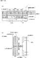
- FIG. 1 is a block diagram illustrating a configuration of an imaging apparatus 1 according to the first embodiment.
- the imaging device 1 includes an imaging optical system 2, an imaging element 3, and a control unit 4.
- the imaging device 1 is a camera, for example.
- the photographing optical system 2 forms a subject image on the image sensor 3.
- the image sensor 3 captures a subject image formed by the photographing optical system 2 and generates an image signal.
- the image sensor 3 is, for example, a CMOS image sensor.
- the control unit 4 outputs a control signal for controlling the operation of the image sensor 3 to the image sensor 3.
- the control unit 4 functions as an image generation unit that performs various types of image processing on the image signal output from the image sensor 3 and generates image data.
- the photographic optical system 2 may be detachable from the imaging device 1.
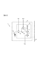
- FIG. 2 is a circuit diagram showing a configuration of the pixel 10 according to the first embodiment.
- the image sensor 3 has a plurality of pixels 10 arranged in a two-dimensional manner.
- the pixel 10 includes a photoelectric conversion unit 12 such as a photodiode (PD) and a reading unit 20.
- the photoelectric conversion unit 12 has a function of converting incident light into charges and accumulating the photoelectrically converted charges.
- the reading unit 20 includes a transfer unit 13, a discharge unit 14, a floating diffusion (FD) 15, an amplification unit 16, and a selection unit 17.
- FD floating diffusion
- the transfer unit 13 is controlled by the signal Vtx and transfers the electric charge photoelectrically converted by the photoelectric conversion unit 12 to the floating diffusion 15. That is, the transfer unit 13 forms a charge transfer path between the photoelectric conversion unit 12 and the floating diffusion 15.
- the floating diffusion 15 holds (accumulates) electric charges.
- the amplifying unit 16 amplifies the signal based on the charge held in the floating diffusion 15 and outputs the amplified signal to the vertical signal line 30 via the selection unit 17.
- the amplifying unit 16 includes a transistor M3 whose drain terminal, gate terminal, and source terminal are connected to the power supply VDD, the floating diffusion 15, and the selection unit 17, respectively.
- the source terminal of the amplifying unit 16 is connected to the vertical signal line 30 via the selecting unit 17.
- the amplifying unit 16 functions as a part of a source follower circuit using a current source 60 described later as a load current source.
- the discharge unit (reset unit) 14 is controlled by the signal Vrst, discharges the charge of the floating diffusion 15, and resets the potential of the floating diffusion 15 to the reset potential (reference potential).
- the selection unit 17 is controlled by the signal Vsel and outputs the signal from the amplification unit 16 to the vertical signal line 30.
- the transfer unit 13, the discharge unit 14, and the selection unit 17 are configured by, for example, a transistor M1, a transistor M2, and a transistor M4, respectively.
- the reading unit 20 receives a signal (photoelectric conversion signal) corresponding to the charge transferred from the photoelectric conversion unit 12 to the floating diffusion 15 by the transfer unit 13 and a signal (noise signal) when the potential of the floating diffusion 15 is reset to the reset potential. ) To the vertical signal line 30.
- the noise signal is a reference signal indicating a reference level for the photoelectric conversion signal.
- the amplification unit 16 and the selection unit 17 constitute an output unit that outputs a signal based on the electric charge accumulated in the floating diffusion 15, and the output unit outputs a photoelectric conversion signal and a noise signal to the vertical signal line 30.
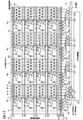
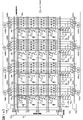
- FIG. 3 is a circuit diagram showing a configuration of a part of the image sensor 3 according to the first embodiment.
- the image pickup device 3 includes a plurality of pixels 10 arranged in a matrix, a vertical scanning circuit 40, a selection circuit 50, a current source 60 (current source 60a to current source 60d), and a first switch unit 70 (first switch).
- Switch unit 70a to first switch unit 70d second switch unit 80 (second switch unit 80a to second switch unit 80d), storage unit 90 (storage unit 90a to storage unit 90d), and horizontal scanning circuit 100
- FIG. 3 is a circuit diagram, and the storage unit 90 is drawn side by side with the pixels 10 for easy understanding.
- the pixels 10 are stacked on a semiconductor substrate in a pixel region in which the pixels 10 are densely arranged in a matrix.
- the storage unit 90 is arranged.
- the pixel region is a region in which a plurality of pixels 10 each having the photoelectric conversion unit 12 and the reading unit 20 are arranged two-dimensionally. That is, in the pixel region, a plurality of pixels 10 are arranged in a first direction (for example, the column direction) and a second direction (for example, the row direction) intersecting with the first direction (for example, the column direction).
- Peripheral circuits (such as the vertical scanning circuit 40 and the horizontal scanning circuit 100) are disposed outside the pixel region.
- a storage unit 90a is provided in the pixel region in which the first pixel column at the left end is arranged, and a storage unit 90b is provided in the pixel region in which the second pixel column on the right is arranged. .
- a storage unit 90c and a storage unit 90d are provided corresponding to the third pixel column and the fourth pixel column on the right side, respectively.
- the accumulation unit 90 is provided by being stacked on a semiconductor substrate in the pixel region.
- the accumulation unit 90 is arranged in parallel with the pixel 10 in the direction in which the accumulation unit 90 is stacked on the semiconductor substrate. For this reason, a large capacitance value can be obtained without increasing the chip area.
- a storage unit 90, a current source 60, a first switch unit 70, and a second switch unit 80 are provided for each pixel column including a plurality of pixels 10 arranged in the column direction, that is, in the vertical direction. That is, in FIG. 3, a storage unit 90, a current source 60, a first switch unit 70, and a second switch unit 80 are provided corresponding to the first pixel column at the left end. Corresponding to the second pixel column, corresponding to the right third pixel column, corresponding to the right fourth pixel column, the storage unit 90, A current source 60, a first switch unit 70, and a second switch unit 80 are provided.
- a vertical signal line 30 (vertical signal line 30a to vertical signal line 30d) is provided corresponding to each column of the pixels 10.
- a vertical signal line 30 vertical signal line 30a to vertical signal line 30d
- pixel in the horizontal direction 4 pixels ⁇ the pixel in the vertical direction 4 is illustrated in order to simplify the description.
- the current sources 60a to 60d are provided corresponding to the vertical signal lines 30a to 30d, respectively, and are connected to the vertical signal lines 30a to 30d.
- the current sources 60a to 60d are connected to the pixels 10 via the vertical signal lines 30a to 30d, respectively.
- the current sources 60a to 60d generate currents for reading out photoelectric conversion signals and noise signals from the respective pixels 10.
- the current sources 60a to 60d supply the generated currents to the vertical signal lines 30a to 30d and each pixel 10, respectively.
- the vertical scanning circuit 40 supplies control signals such as the signal Vtxn, the signal Vrstn, and the signal Vseln to each pixel 10.
- the vertical scanning circuit 40 outputs a signal Vtxn or the like to each pixel 10 to control the operation of each pixel 10.
- n at the end of Vtxn, Vrstn, and Vseln indicates the row number of the pixel.
- the signal Vtx1 is a signal that controls the transfer unit 13 of the pixels 10 in the first row.
- the first switch unit 70a to the first switch unit 70d are provided corresponding to the vertical signal line 30a to the vertical signal line 30d, respectively, and are connected to the vertical signal line 30a to the vertical signal line 30d.
- the first switch unit 70a to the first switch unit 70d switch the electrical connection state between the vertical signal line 30a to the vertical signal line 30d and the storage unit 90a to the storage unit 90d.
- the first switch unit 70a to the first switch unit 70d are controlled by the control signal output from the selection circuit 50, and the photoelectric conversion signal and the noise signal output from each pixel 10 are respectively stored in the storage units 90a to 90d. Forward.
- Each of the first switch unit 70a to the first switch unit 70d includes a switch TN1, a switch TS1, a switch TN2, and a switch TS2.
- the switch TN1, the switch TS1, the switch TN2, and the switch TS2 are each configured by a transistor.
- the second switch unit 80a to the second switch unit 80d are provided corresponding to the vertical signal line 30a to the vertical signal line 30d, respectively.
- the second switch unit 80a to the second switch unit 80d switch the electrical connection state between the storage units 90a to 90d and the output amplifier unit 110.
- the second switch unit 80a to the second switch unit 80d are controlled by a control signal output from the horizontal scanning circuit 100, and convert the photoelectric conversion signals and noise signals stored in the storage units 90a to 90d into the horizontal signal line S. Then, the data is transferred to the output amplifier unit 110 via the horizontal signal line N.
- Each of the second switch unit 80a to the second switch unit 80d includes a switch PH1N, a switch PH1S, a switch PH2N, and a switch PH2S.
- Switch PH1N, switch PH1S, switch PH2N, and switch PH2S are each configured by a transistor.
- the selection circuit 50 supplies control signals such as the signal Vtn1, the signal Vts1, the signal Vtn2, and the signal Vts2 to the first switch unit 70a to the first switch unit 70d.
- the selection circuit 50 outputs a control signal to control the operations of the first switch unit 70a to the first switch unit 70d.
- the horizontal scanning circuit 100 supplies control signals such as the signal Vph11, the signal Vph12, the signal Vph21, the signal Vph22, the signal Vph31, the signal Vph32, the signal Vph41, and the signal Vph42 to the second switch unit 80a to the second switch unit 80d.
- the horizontal scanning circuit 100 outputs a control signal to control operations of the second switch unit 80a to the second switch unit 80d.
- the accumulation units 90a to 90d are provided corresponding to the columns of the pixels 10 and accumulate (store) photoelectric conversion signals and noise signals output from the pixels 10.
- the accumulating units 90a to 90d have a capacity for accumulating photoelectric conversion signals and noise signals.
- the capacity is, for example, a capacity due to a conductor, such as a capacity formed by adjacent metals. Specifically, for example, the capacitance is formed between a conductor to which a photoelectric conversion signal or a noise signal is input and a conductor to which a predetermined potential is applied.
- each of the storage units 90a to 90d has conductors CN1 and CN2 to which noise signals are input, and conductors CS1 and CS2 to which photoelectric conversion signals are input. Further, each of the storage units 90a to 90d has a fixed potential line 120 as a conductor to which the above-described predetermined potential is applied. In FIG. 3, the fixed potential line 120 is indicated by a dotted line in order to distinguish it from the conductor CN1, the conductor CS1, the conductor CN2, and the conductor CS2.
- a symbol C indicating a plurality of capacitances shown in FIG. 3 is between the conductor CN1 and the fixed potential line 120, between the conductor CS1 and the fixed potential line 120, between the conductor CN2 and the fixed potential line 120, and between the conductor CS2 and This schematically shows that capacitors are formed between the fixed potential line 120 and each other.
- the conductors CN1 and CN2 function as a noise accumulation unit that accumulates noise signals
- the conductors CS1 and CS2 function as a signal accumulation unit that accumulates photoelectric conversion signals.
- the output amplifier unit 110 outputs a signal based on the difference between the noise signal input via the horizontal signal line N and the photoelectric conversion signal input via the horizontal signal line S to the output terminal shown in FIG. For example, the output amplifier unit 110 outputs a signal obtained by amplifying the difference between the noise signal and the photoelectric conversion signal with a predetermined gain.
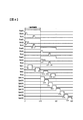
- FIG. 4 is a timing chart showing an operation example of the image sensor 3 according to the first embodiment.
- the vertical axis represents the voltage level of the control signal
- the horizontal axis represents time.
- a control signal when a control signal is at a high level (for example, a power supply potential), the transistor to which the control signal is input is turned on, and when the control signal is at a low level (for example, a ground potential), the control signal is input.
- the transistor to be turned off is turned off.
- Each of time t1 to time t10, time t10 to time t22, time t22 to time t34, time t34 to time t46, and time t46 to time t50 is one horizontal period.
- the charge accumulated in the photoelectric conversion unit 12 is reset in synchronization with the discharge of the floating diffusion 15, that is, the reset of the floating diffusion 15.
- a description of resetting the photoelectric conversion unit 12 is omitted.
- the signal Vsel1 becomes a high level, whereby the transistor M4 of the selection unit 17 is turned on in each pixel 10 in the first row.
- the signal Vrst1 becomes high level, so that the transistor M2 of the discharge unit 14 is turned on in each pixel 10 in the first row.
- the potential of the floating diffusion 15 becomes the reset potential.
- the noise signal of each pixel 10 in the first row is output to the vertical signal line 30a to the vertical signal line 30d by the amplification unit 16 and the selection unit 17, respectively.
- the signal Vrst1 becomes low level, so that the transistor M2 is turned off.
- the signal Vtn1 becomes a high level, so that the switches TN1 of the first switch unit 70a to the first switch unit 70d are turned on. As a result, the noise signal from each pixel 10 is transferred to the conductor CN1 of the storage units 90a to 90d.
- the capacitors added to the conductors CN1 of the storage units 90a to 90d store noise signals from the respective pixels 10 in the first row.
- the signal Vtn1 becomes low level, so that the switch TN1 is turned off. When the switch TN1 is turned off, the capacitor added to the conductor CN1 holds (accumulates) the noise signal.
- the transistor M1 of the transfer unit 13 is turned on in each pixel 10 in the first row. Thereby, the electric charge photoelectrically converted by the photoelectric conversion unit 12 is transferred to the floating diffusion 15. Further, the photoelectric conversion signal of each pixel 10 in the first row is output to the vertical signal line 30a to the vertical signal line 30d by the amplification unit 16 and the selection unit 17. At time t7, the signal Vtx1 becomes low level, so that the transistor M1 is turned off. At time t8, since the signal Vts1 becomes high level, the switches TS1 of the first switch unit 70a to the first switch unit 70d are turned on.
- the photoelectric conversion signal is transferred to the conductor CS1 of the storage units 90a to 90d.
- the capacitance added to the conductor CS1 accumulates photoelectric conversion signals from the pixels 10 in the first row.
- the signal Vts1 becomes low level, so that the switch TS1 is turned off.
- the capacitor added to the conductor CS1 holds the photoelectric conversion signal.
- the signal Vph11 and the signal Vsel2 become high level.
- the switch PH1N and the switch PH1S of the second switch unit 80a are turned on.
- signals from the pixels 10 in the first row accumulated in the accumulation unit 90a corresponding to the first column of each pixel 10 are output to the horizontal signal line S and the horizontal signal line N. That is, the photoelectric conversion signal stored in the conductor CS1 of the storage unit 90a is output to the horizontal signal line S, and the noise signal stored in the conductor CN1 of the storage unit 90a is output to the horizontal signal line N.
- the output amplifier unit 110 outputs a signal based on the difference between the noise signal and the photoelectric conversion signal.
- the transistor M4 of each pixel 10 in the second row is turned on.
- the signal Vrst2 becomes high level, so that the transistor M2 is turned on and the floating diffusion 15 is reset.
- the noise signal of each pixel 10 in the second row is output to the vertical signal line 30a to the vertical signal line 30d.
- the signal Vrst2 becomes low level, and the transistor M2 is turned off.
- the signal Vtn2 becomes high level, so that the switch TN2 is turned on.
- the noise signal is transferred to the conductor CN2 of the storage units 90a to 90d.
- the capacitance added to the conductor CN2 accumulates a noise signal from each pixel 10 in the second row.
- the signal Vph11 becomes low level and the signal Vph21 becomes high level.
- the switch PH1N and the switch PH1S of the second switch unit 80a are turned off.
- the switch PH1N and the switch PH1S of the second switch unit 80b are turned on.
- the photoelectric conversion signal from the pixel 10 in the first row accumulated in the accumulation unit 90b corresponding to the second column of each pixel 10 is output to the horizontal signal line S, and the noise signal is output to the horizontal signal line N. Is done.
- the output amplifier unit 110 outputs a signal based on the difference between the noise signal and the photoelectric conversion signal.
- the signal Vtn2 becomes low level, so that the switch TN2 is turned off.
- the capacitance added to the conductor CN2 holds the noise signal.
- the signal Vph21 becomes low level and the signal Vph31 becomes high level.
- the switch PH1N and the switch PH1S of the second switch unit 80b are turned off.
- the switch PH1N and the switch PH1S of the second switch unit 80c are turned on.
- the photoelectric conversion signal from the pixel 10 in the first row accumulated in the accumulation unit 90c corresponding to the third column of each pixel 10 is output to the horizontal signal line S, and the noise signal is output to the horizontal signal line N. Is done.
- the output amplifier unit 110 outputs a signal based on the difference between the noise signal and the photoelectric conversion signal.
- the signal Vtx2 becomes high level, so that the transistor M1 is turned on in each pixel 10 in the second row. Thereby, the electric charge photoelectrically converted by the photoelectric conversion unit 12 is transferred to the floating diffusion 15. Further, the photoelectric conversion signal of each pixel 10 in the second row is output to the vertical signal line 30a to the vertical signal line 30d. At time t18, the signal Vtx2 becomes low level, so that the transistor M1 is turned off. At time t19, since the signal Vts2 becomes high level, the switches TS2 of the first switch unit 70a to the first switch unit 70d are turned on. As a result, the photoelectric conversion signal is transferred to the conductor CS2 of the storage units 90a to 90d. The capacitance added to the conductor CS2 accumulates photoelectric conversion signals from the pixels 10 in the second row.
- the signal Vph31 becomes low level and the signal Vph41 becomes high level.
- the switch PH1N and the switch PH1S of the second switch unit 80c are turned off.
- the switch PH1N and the switch PH1S of the second switch unit 80d are turned on.
- the photoelectric conversion signal from the pixel 10 in the first row accumulated in the accumulation unit 90d corresponding to the fourth column of each pixel 10 is output to the horizontal signal line S, and the noise signal is output to the horizontal signal line N. Is done.
- the output amplifier unit 110 outputs a signal based on the difference between the noise signal and the photoelectric conversion signal.
- the signal Vts2 becomes low level, so that the switch TS2 is turned off.
- the capacitor added to the conductor CS2 holds the photoelectric conversion signal.
- the signals from the pixels 10 in the first row accumulated in the storage unit 90 are read out from the pixels 10 in the second row to the storage unit 90. Is transferred to the horizontal signal line S and the horizontal signal line N.
- the signal Vph41 becomes low level, and the signal Vph12 and the signal Vsel3 become high level.
- the switch PH1N and the switch PH1S of the second switch unit 80d are turned off.
- the switch PH2N and the switch PH2S of the second switch unit 80a are turned on.
- signals from the pixels 10 in the second row accumulated in the accumulation unit 90 a corresponding to the first column of the pixels 10 are output to the horizontal signal line S and the horizontal signal line N.
- the photoelectric conversion signal stored in the conductor CS2 of the storage unit 90a is output to the horizontal signal line S
- the noise signal stored in the conductor CN2 of the storage unit 90a is output to the horizontal signal line N.
- the output amplifier unit 110 outputs a signal based on the difference between the noise signal and the photoelectric conversion signal.
- the transistor M4 of each pixel 10 in the third row is turned on.
- the signal Vrst3 becomes high level, so that the transistor M2 is turned on and the floating diffusion 15 is reset.
- the noise signal of each pixel 10 in the third row is output to the vertical signal line 30a to the vertical signal line 30d.
- the signal Vrst3 becomes low level, and the transistor M2 is turned off.
- the signal Vtn1 becomes high level, so that the switch TN1 is turned on.
- the noise signal is transferred to the conductor CN1 of the storage units 90a to 90d.
- the capacitance added to the conductor CN1 accumulates a noise signal from each pixel 10 in the third row.
- the signal Vph12 becomes low level and the signal Vph22 becomes high level.
- the switch PH2N and the switch PH2S of the second switch unit 80a are turned off.
- the switch PH2N and the switch PH2S of the second switch unit 80b are turned on.
- the photoelectric conversion signal from each pixel 10 in the second row accumulated in the accumulation unit 90b corresponding to the second column of each pixel 10 is output to the horizontal signal line S, and the noise signal is applied to the horizontal signal line N. Is output.
- the output amplifier unit 110 outputs a signal based on the difference between the noise signal and the photoelectric conversion signal.
- the signal Vtn1 becomes low level, so that the switch TN1 is turned off.
- the capacitor added to the conductor CN1 holds the noise signal.
- the signal Vph22 becomes low level and the signal Vph32 becomes high level.
- the switch PH2N and the switch PH2S of the second switch unit 80b are turned off.
- the switch PH2N and the switch PH2S of the second switch unit 80c are turned on.
- the photoelectric conversion signal from each pixel 10 in the second row accumulated in the accumulation unit 90c corresponding to the third column of each pixel 10 is output to the horizontal signal line S, and the noise signal is output to the horizontal signal line N. Is output.
- the output amplifier unit 110 outputs a signal based on the difference between the noise signal and the photoelectric conversion signal.
- the signal Vtx3 becomes high level, so that the transistor M1 is turned on in each pixel 10 in the third row. Thereby, the electric charge photoelectrically converted by the photoelectric conversion unit 12 is transferred to the floating diffusion 15. Further, the photoelectric conversion signal of each pixel 10 in the third row is output to the vertical signal line 30a to the vertical signal line 30d. At time t30, the signal Vtx3 becomes low level, so that the transistor M1 is turned off. At time t31, since the signal Vts1 becomes high level, the switches TS1 of the first switch unit 70a to the first switch unit 70d are turned on. As a result, the photoelectric conversion signal is transferred to the conductor CS1 of the storage units 90a to 90d. The capacitance added to the conductor CS1 accumulates photoelectric conversion signals from the pixels 10 in the third row.
- the signal Vph32 becomes low level and the signal Vph42 becomes high level.
- the switch PH2N and the switch PH2S of the second switch unit 80c are turned off.
- the switch PH2N and the switch PH2S of the second switch unit 80d are turned on.
- the output amplifier unit 110 outputs a signal based on the difference between the noise signal and the photoelectric conversion signal.
- the switch TS1 is turned off.
- the capacitor added to the conductor CS1 holds the photoelectric conversion signal.
- the transistors controlled by the signals Vsel4, Vrst4, Vtn2, Vtx4, and Vts2 are sequentially turned on and off in the same manner as in the period from time t10 to time 22 and from time t22 to time 34.
- the noise signal from each pixel 10 in the fourth row is accumulated in the capacitor added to the conductor CN2, and the photoelectric conversion signal from each pixel 10 in the fourth row is accumulated in the capacitor added to the conductor CS2.
- the transistors controlled by the signals Vph11, Vph21, Vph31, and Vph41 are sequentially turned on and off.
- the noise signal and the photoelectric conversion signal from each pixel 10 in the third row stored in the storage units 90a to 90d are sequentially output.
- the output amplifier unit 110 sequentially outputs signals based on the difference between the noise signal output from the storage units 90a to 90d and the photoelectric conversion signal.
- the transistors controlled by the signals Vph12, Vph22, Vph32, and Vph42 are sequentially turned on and off.
- the noise signal and the photoelectric conversion signal from each pixel 10 in the fourth row respectively stored in the storage units 90a to 90d are sequentially output.
- the output amplifier unit 110 sequentially outputs signals based on the difference between the noise signal output from the storage units 90a to 90d and the photoelectric conversion signal.
- the signals from the pixels 10 in a certain row to the storage unit 90 are transmitted to the horizontal signal line S.
- the horizontal transfer to the horizontal signal line N is performed.
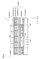
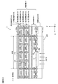
- FIG. 5 is a diagram illustrating an example of a cross-sectional structure of the image sensor 3 according to the first embodiment.
- FIG. 5 is a cross-sectional view taken along the line A-A ′ in FIG. 6 to be described later.
- the imaging device 3 is, for example, a backside illumination type imaging device.
- the incident light is incident mainly in the positive direction of the Z axis.
- the left direction on the paper orthogonal to the Z axis is defined as the X axis plus direction
- the back direction on the paper orthogonal to the Z axis and the X axis is defined as the Y axis plus direction.
- the coordinate axes are displayed so that the orientation of each figure can be understood with reference to the coordinate axes in FIG.
- the imaging device 3 includes a semiconductor substrate 200 made of a semiconductor material such as silicon and a wiring layer 210 stacked on the semiconductor substrate 200.
- the image sensor 3 further includes a microlens layer, a color filter layer, and a passivation layer (not shown).
- the imaging element 3 is arranged in the order of the microlens layer, the color filter layer, the passivation layer, the semiconductor substrate 200, and the wiring layer 210 in the positive direction of the Z axis.
- the semiconductor substrate 200 has a first surface 201a serving as an incident surface on which light is incident, and a second surface 201b different from the first surface 201a.
- the second surface 201b is positioned opposite to the first surface 201a.
- the back surface of the imaging device 3 shows the first surface 201a located on the opposite side to the wiring layer 210, and the back-illuminated type is configured such that light enters from the first surface 201a serving as the back surface.
- the wiring layer 210 has a surface (third surface 203a) on the second surface 201b side of the semiconductor substrate 200 and a surface opposite to the third surface 203a (fourth surface 203b).
- the semiconductor substrate 200 includes the photoelectric conversion unit 12 and the reading unit 20 between the first surface 201a and the second surface 201b.
- a plurality of pixels 10 each including the photoelectric conversion unit 12 and the reading unit 20 are arranged in the X-axis direction and the Y-axis direction.
- the photoelectric conversion unit 12 converts incident light incident from one side of the semiconductor substrate 200, that is, the first surface 201 a side of the semiconductor substrate 200 into electric charge.
- the accumulation unit 90 is provided so as to be stacked with the photoelectric conversion unit 12 on the side opposite to one side of the semiconductor substrate 200, that is, on the second surface 201 b side of the semiconductor substrate 200.
- the storage unit 90 is provided between the photoelectric conversion unit 12 and the fourth surface 203 b of the wiring layer 210.
- a multilayer wiring layer 210 including a conductor film (metal film) and an insulating film is formed on the second surface 201b of the semiconductor substrate 200.
- a plurality of wirings and vias are arranged. Copper, aluminum, or the like is used for the conductor film.
- the insulating film includes an insulating film between the conductor films, a gate insulating film, and the like, and is configured by an oxide film, a nitride film, or the like.
- the wiring layer 210 includes a signal wiring layer 211 provided with signal lines such as control signals Vtxn, Vrstn, and Vseln input to each pixel 10 and a vertical signal line 30, and an accumulation unit 90 (accumulation units 90a to 90d). And an accumulating portion wiring layer 212.
- the signal wiring layer 211 is stacked on the second surface 201b of the semiconductor substrate 200, and the storage unit wiring layer 212 is stacked on the signal wiring layer 211a.
- the storage unit wiring layer 212 is formed by stacking the storage unit 90 a corresponding to the first pixel column via the signal wiring layer 211 in the pixel region where the first pixel column is located. Then, in the pixel region where the second pixel row is located, a storage unit 90b corresponding to the second pixel row is stacked via the signal wiring layer 211, and similarly, the pixels in the third row are stacked. Storage units 90 c and 90 d corresponding to the column and the fourth pixel column are stacked via the signal wiring layer 211. In this way, each of the storage units 90a to 90d of the storage unit wiring layer 212 is provided in each pixel region 220 for each corresponding pixel column.
- Each of the storage portions 90a to 90d of the storage portion wiring layer 212 has a size corresponding to the pixels 10 for one column.
- the storage units 90a to 90d of the storage unit wiring layer 212 have the same configuration, and the storage unit 90 shown in FIG. 5 corresponds to any one of the storage units 90a to 90d.
- the storage unit 90 includes the conductor CN1, the conductor CS1, the conductor CN2, the conductor CS2, and the fixed potential line 120 as described above.
- the fixed potential line 120 includes a first fixed potential line 120 a, a second fixed potential line 120 b, and a third fixed potential line 120 c, each of which is constituted by a conductor film of a different layer.
- the first fixed potential line 120 a and the third fixed potential line 120 c are arranged apart from each other in the Z-axis direction, which is the stacking direction of the wiring layers 210.
- the first fixed potential line 120a and the third fixed potential line 120c are common to all the accumulation units 90a, 90b, 90c, and 90d, and are thus formed so as to cover all the pixels 10 of the image sensor 3.
- the first fixed potential line 120a and the third fixed potential line 120c may be configured in common for all the storage units as described above, or may be configured for each storage unit.
- the conductor CN1, the conductor CS1, the conductor CN2, and the conductor CS2 extend in the arrangement direction of the plurality of pixels 10 constituting each pixel column.
- the conductors CN1, CS1, CN2, and CS2 are disposed between the first fixed potential line 120a and the third fixed potential line 120c and separated from the first fixed potential line 120a and the third fixed potential line 120c.
- the second fixed potential line 120b is disposed between each of the conductors CN1, CS1, CN2, and CS2, and is connected to the first fixed potential line 120a and the third fixed potential line 120c through vias.
- An insulating film is provided between the conductors CN1, CS1, CN2, and CS2 and the first to third fixed potential lines 120a to 120c.
- the insulating film is an oxide film or a nitride film. Specifically, a silicon oxide film, a silicon nitride film, a silicon oxynitride film, or a multilayer film
- capacitance is formed between each of the conductors CN1, CS1, CN2, and CS2 and the first to third fixed potential lines 120a to 120c.
- the capacitance can be increased.
- a high dielectric material having a dielectric constant higher than that of a silicon oxide film or the like may be used.
- an MIM capacity may be used. Note that a capacitance formed between the conductors CN1, CS1, CN2, and CS2 and a wiring different from the fixed potential line is also added.
- the first fixed potential line 120a, the second fixed potential line 120b, and the third fixed potential line 120c are given a predetermined potential such as a power supply potential or a ground potential.
- the first fixed potential line 120a functions as a shield between the vertical signal line 30 and the control signal line of the signal wiring layer 211 and the conductors CN1, CS1, CN2, and CS2.
- By providing the first fixed potential line 120a it is possible to suppress the formation of a large parasitic capacitance between the vertical signal line 30, the control signal line, and the like and the conductors CN1, CS1, CN2, and CS2. Further, crosstalk between the vertical signal line 30, the control signal line, and the like and the conductors CN1, CS1, CN2, and CS2 can be suppressed.
- the first fixed potential line 120a, the second fixed potential line 120b, and the third fixed potential line 120c are provided so as to surround each of the conductors CN1, CS1, CN2, and CS2, so that the conductors CN1, CS1 , CN2 and CS2 function as a shield.
- a large parasitic capacitance can be avoided between the conductors CN1, CS1, CN2, and CS2, and crosstalk between the conductors CN1, CS1, CN2, and CS2 can be suppressed.
- the first fixed potential line 120a is set to the ground potential and is connected to the semiconductor substrate 200 via the via 202 or the like.
- the first fixed potential line 120 a is commonly connected to each pixel 10 as a ground line (ground line) for supplying a ground potential to each pixel 10.
- a power supply potential may be applied to the first fixed potential line 120a so that the pixel 10 is used as a common power supply line.
- the fixed potential line is shared by the conductors for forming the capacitances of the conductors CN1, CS1, CN2, and CS2, the shield for suppressing the mixing of noise, and the power supply line or the ground line of each pixel 10. .
- the fixed potential line By using the fixed potential line as a power supply line or a ground line for each pixel 10, it is not necessary to separately provide a wiring for the power supply line or the ground line. For this reason, the number of wiring layers 210 can be reduced.
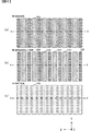
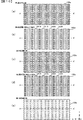
- FIG. 6 is a diagram illustrating an example of a planar layout of a part of the storage unit wiring layer 212 of the image sensor 3 according to the first embodiment.
- FIG. 6A shows an example of a planar layout of a layer in which the third fixed potential line 120c is formed
- FIG. 6B shows the second fixed potential line 120b and conductors CN1, CS1, CN2, and CS2.
- FIG. 6C is a diagram illustrating an example of a planar layout of a layer on which the first fixed potential line 120a is formed.
- the third fixed potential line 120c and the first fixed potential line 120a are formed in a planar shape as shown in FIG.
- the third fixed potential line 120c and the first fixed potential line 120a are formed so as to cover all the pixels 10 that are two-dimensionally arranged in a matrix, for example.
- the second fixed potential line 120b, the conductor CN1, the conductor CS1, the conductor CN2, and the conductor CS2 are each formed in a linear shape.
- the second fixed potential line 120b is disposed to face the conductors CN1, CS1, CN2, and CS2.
- the length of the second fixed potential line 120b in the Y-axis direction is a length corresponding to the length of the conductors CN1, CS1, CN2, and CS2 in the Y-axis direction.
- the storage units 90a to 90d are provided corresponding to the pixel columns of the respective pixels 10, the lengths of the second fixed potential line 120b and the conductors CN1, CS1, CN2, and CS2 in the Y-axis direction The length corresponds to one pixel column.
- the third fixed potential line 120c and the second fixed potential line 120b are connected via a plurality of vias, and the second fixed potential line 120b and the first fixed potential line 120a are connected via a plurality of vias.
- the imaging device 3 includes a photoelectric conversion unit 12 that converts incident light incident from one side of the substrate 200 into charges, and an output unit (amplification unit 16 and selection unit 17) that outputs a signal based on charges.
- the plurality of pixels 10 arranged in the first direction and the second direction intersecting the first direction are stacked with the photoelectric conversion unit 12 on the side opposite to the one side of the substrate 200 to accumulate signals.
- an accumulation unit 90 is provided by being stacked on the second surface 201 b of the semiconductor substrate 200 in the pixel region 220.
- the chip area of the image sensor is increased by providing a large number of capacitors in a region where an analog / digital conversion circuit and the like around the pixel region 220 are arranged.
- the accumulation unit 90 is provided by being stacked on the second surface 201b of the semiconductor substrate 200. For this reason, an increase in chip area can be suppressed.
- the storage unit 90 in the pixel region 220, it is possible to avoid an increase in the area of the region where the analog / digital conversion circuit and the like around the pixel region 220 are arranged.
- a large capacity can be formed by providing a capacity corresponding to one pixel column or the like.
- the imaging device 3 includes a photoelectric conversion unit 12 that converts light incident on the first surface 201a of the semiconductor substrate 200 into charges, and a readout unit 20 that outputs a signal due to charges on the second surface 201b of the semiconductor substrate 200.
- a storage unit 90 that is stacked on the pixel region 220 of the second surface 201b and stores the signal output from the readout unit 20. Since it did in this way, the increase in a chip area can be suppressed.
- the storage unit 90 is commonly connected to the plurality of pixels 10 arranged in the first direction. Since it did in this way, a capacity
- the imaging device 3 further includes a signal line (vertical signal line 30) that is connected in common to the plurality of pixels 10 arranged in the first direction and that outputs a signal from the readout unit 20.
- the storage unit 90 is commonly connected to the plurality of pixels 10 via signal lines. Since it did in this way, the signal from each pixel 10 read via the vertical signal line 30 can be stored in the storage unit 90.
- the reading unit 20 outputs a signal based on charges and a noise signal.
- the accumulating unit 90 includes a signal accumulating unit that accumulates signals based on electric charges, and a noise accumulating unit that accumulates noise signals. Since it did in this way, the photoelectric conversion signal and noise signal which are output from the read-out part 20 can be accumulated in accumulation part 90, respectively.
- first wiring (second fixed potential line 120b) provided between the signal storage unit and the noise storage unit to which a constant potential (for example, a power supply potential or a ground potential) is applied;
- a second wiring (first fixed potential line 120a) provided between the storage unit 90 and a constant potential is applied to the side opposite to the light incident side, with the storage unit 90 and the insulating film interposed therebetween.
- a third wiring (third fixed potential line 120c) to which a constant potential is applied.
- the first fixed potential line 120a, the second fixed potential line 120b, and the third fixed potential line 120c are provided so as to surround each of the conductors CN1, CS1, CN2, and CS2. For this reason, mixing of noise can be suppressed.
- the storage unit 90 includes a first storage unit (for example, a storage unit 90a) connected to the plurality of pixels 10 arranged in the first direction, and a plurality of units arranged in the first direction different from the plurality of pixels 10.
- a second storage unit (for example, storage unit 90b) connected to the pixel, and a plurality of first storage units and second storage units are provided side by side in the second direction. Since it did in this way, the accumulation
- the reading unit 90 includes a holding unit 15 that holds the charge converted by the photoelectric conversion unit 12, a transfer unit 13 that transfers the charge to the holding unit 15, and a discharge that discharges the charge held by the holding unit 15. And an amplifying unit 16 that amplifies a signal based on the charges transferred by the transfer unit 13. Since it did in this way, the photoelectric conversion signal based on the electric charge photoelectrically converted by the photoelectric conversion part 12 from each pixel 10 can be read. (9)
- the noise signal is a signal when the electric charge held in the holding unit 15 is discharged. Since it did in this way, the noise signal used as the reference level with respect to a photoelectric conversion signal can be obtained.
- the imaging device 3 includes a photoelectric conversion unit 12 that converts light incident on the first surface 201a of the semiconductor substrate 200 into electric charge, and a reading unit 20 that outputs a signal based on electric charge to the second surface 201b of the semiconductor substrate 200. , And a second layer (storage portion wiring layer 212) that is stacked on the first layer on the second surface 201 b and has a storage portion 90 that stores the signal output by the reading portion 20. And). Since this is done, a large capacitance value can be obtained without increasing the chip area. (11)
- the storage unit 90 has a capacitance due to a conductor. Since it did in this way, increase of a chip area can be suppressed compared with the case where diffusion capacity is provided.
- the imaging device 3 includes a photoelectric conversion unit 12 that converts incident light into electric charges, a first accumulation unit (floating diffusion 15) to which electric charges converted by the photoelectric conversion unit 12 are transferred, and a first Pixels 10 having an output unit (amplifying unit 16 and selection unit 17) for outputting a signal based on the charge transferred to the storage unit, and a pixel based on the charge transferred from the photoelectric conversion unit 12 to the first storage unit
- An output control unit (vertical scanning circuit 40) that switches a signal (photoelectric conversion signal) and a reset signal (noise signal) that resets the charge of the first accumulation unit to output from the output unit, and is output from the output unit
- the pixel 10 is disposed between the light incident surface and the second accumulation unit or the third accumulation unit. Since it did in this way, the increase in a chip area can be suppressed
- the imaging device according to the second embodiment has a configuration similar to that of the imaging device 1 according to the first embodiment.
- the image sensor according to the second embodiment is different from the first embodiment mainly in that a plurality of vertical signal lines are provided for each pixel column to simultaneously read out the pixels 10 in a plurality of rows.
- the same or corresponding parts as those in the first embodiment are denoted by the same reference numerals, and differences will mainly be described.
- FIG. 7 is a circuit diagram showing a partial configuration of the image sensor 3 according to the second embodiment.
- two vertical signal lines (vertical signal line 30 ⁇ / b> A and vertical signal line 30 ⁇ / b> B) are provided corresponding to each column of the pixels 10.
- the pixels 10 in each column are connected to different vertical signal lines for each row.
- the imaging device 3 includes a selection circuit 50 (selection circuit 50A and selection circuit 50B), and a current source 60 (current source 60A1 to current source 60A3, current source 60B1 to current source 60B3).
- the first switch unit 70 (first switch unit 70A1 to first switch unit 70A3, first switch unit 70B1 to first switch unit 70B3), and second switch unit 80 (second switch unit 80A1 to second switch unit 80A3) , Second switch unit 80B1 to second switch unit 80B3), storage unit 90 (storage unit 90A1 to storage unit 90A3, storage unit 90B1 to storage unit 90B3), and horizontal scanning circuit 100 (horizontal scanning circuit 100A and horizontal scanning circuit). 100B) and the output amplifier unit 110 (the output amplifier unit 110A and the output amplifier unit 110B).
- the pixel 10 shows only 3 pixels in the horizontal direction ⁇ 4 pixels in the vertical direction.
- FIG. 8 is a timing chart showing an operation example of the image sensor 3 according to the second embodiment.
- time t1 to time t10, time t10 to time t22, and time t22 to time t26 are each one horizontal period.
- the signal Vsel1 and the signal Vsel2 are at a high level, whereby the transistor M4 of the selection unit 17 is turned on in each pixel 10 in the first row and the second row.
- the signal Vrst1 and the signal Vrst2 are set to the high level, whereby the transistor M2 of the discharge unit 14 is turned on in each pixel 10 in the first and second rows, and the potential of the floating diffusion 15 is set to the reset potential.
- the noise signal of each pixel 10 in the first row is output to the vertical signal line 30B1 to the vertical signal line 30B3, respectively, and the noise signal of each pixel 10 in the second row is output to the vertical signal line 30A1 to the vertical signal line 30A3, respectively. Is done.
- the signal Vrst1 and the signal Vrst2 are at a low level, so that the transistor M2 is turned off.
- the signal Vtn1 becomes high level, so that the switches TN1 of the first switch unit 70A1 to the first switch unit 70A3 and the first switch unit 70B1 to the first switch unit 70B3 are turned on.
- the noise signal from each pixel 10 in the first row is transferred to the conductor CN1B of the storage unit 90B1 to storage unit 90B3
- the noise signal from each pixel 10 in the second row is transferred to the conductor of the storage unit 90A1 to storage unit 90A3. Transferred to CN1A.
- the signal Vtn1 becomes low level, so that the switch TN1 is turned off.
- the capacitors added to the conductors CN1B of the storage units 90B1 to 90B3 hold the noise signals from the respective pixels 10 in the first row. Further, the capacitors added to the conductors CN1A of the storage units 90A1 to 90A3 hold noise signals from the respective pixels 10 in the second row.
- the signal Vtx ⁇ b> 1 and the signal Vtx ⁇ b> 2 become high level, whereby the transistor M ⁇ b> 1 of the transfer unit 13 is turned on in each pixel 10 in the first row and second row, and the photoelectric conversion unit 12 performs photoelectric conversion.
- the charge is transferred to the floating diffusion 15.
- the photoelectric conversion signals of the pixels 10 in the first row are output to the vertical signal lines 30B1 to 30B3, respectively, and the photoelectric conversion signals of the pixels 10 in the second row are respectively the vertical signal lines 30A1 to 30A3. Is output.
- the signal Vtx1 and the signal Vtx2 are at a low level, so that the transistor M1 is turned off.
- the signal Vts1 becomes high level, so that the switches TS1 of the first switch unit 70A1 to the first switch unit 70A3 and the first switch unit 70B1 to the first switch unit 70B3 are turned on.
- the photoelectric conversion signals from the pixels 10 in the first row are transferred to the conductors CS1B of the storage units 90B1 to 90B3, and the photoelectric conversion signals from the pixels 10 in the second row are stored in the storage units 90A1 to 90A3. Is transferred to the conductor CS1A.
- the signal Vts1 becomes low level, so that the switch TS1 is turned off.
- the capacitors added to the conductors CS1B of the storage units 90B1 to 90B3 hold the photoelectric conversion signals from the respective pixels 10 in the first row.
- the capacitance added to the conductor CS1A of the storage units 90A1 to 90A3 holds the photoelectric conversion signal from each pixel 10 in the second row.
- the signals of the pixels 10 in the first row are read out to the storage units 90B1 to 90B3, and the signals of the pixels 10 in the second row are stored in the storage unit.
- 90A1 to 90A3 are read out.
- the transistors controlled by the signals Vsel3, Vsel4, Vrst3, Vrst4, Vtn2, Vtx3, Vtx4, and Vts2 are sequentially turned on and off as in the case of the period from time t1 to time 10.
- the noise signals and photoelectric conversion signals from the respective pixels 10 in the third row are accumulated in the capacitors added to the conductors CN2B and CS2B of the accumulation units 90B1 to 90B3, respectively.
- noise signals and photoelectric conversion signals from the respective pixels 10 in the fourth row are accumulated in the capacitors added to the conductors CN2A and CS2A of the accumulation units 90A1 to 90A3, respectively.
- the conductors CN1A, CN2A, CN1B, and CN2B function as a noise accumulation unit that accumulates noise signals.
- the conductors CS1A, CS2A, CS1B, and CS2B function as a signal storage unit that stores photoelectric conversion signals.
- the signal Vph11 becomes high level, so that the switches PH1N and PH1S of the second switch unit 80A1 and the second switch unit 80B1 are turned on.
- signals from the pixels 10 in the first row accumulated in the accumulation unit 90B1 are output to the horizontal signal line BS and the horizontal signal line BN.
- signals from the pixels 10 in the second row accumulated in the accumulation unit 90A1 are output to the horizontal signal line AS and the horizontal signal line AN.
- Each of the output amplifier unit 110A and the output amplifier unit 110B outputs a signal based on the difference between the noise signal and the photoelectric conversion signal.
- the transistors controlled by the signals Vph12, Vph22, and Vph32 are sequentially turned on and off.
- the noise signal and the photoelectric conversion signal from each pixel 10 in the third row stored in the storage units 90B1 to 90B3 are sequentially output.
- noise signals and photoelectric conversion signals from the respective pixels 10 in the fourth row stored in the storage units 90A1 to 90A3 are sequentially output.
- the output amplifier unit 110A and the output amplifier unit 110B sequentially output signals based on the difference between the noise signal and the photoelectric conversion signal.
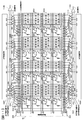
- FIG. 9 is a diagram illustrating an example of a cross-sectional structure of the image sensor 3 according to the second embodiment.
- FIG. 9 is a cross-sectional view taken along line A-A ′ in FIG. 10 to be described later.
- the wiring layer 210 is provided with a storage part wiring layer 212A having a storage part 90A (storage part 90A1 to storage part 90A3) and a storage part wiring layer 212B having storage parts 90B (storage part 90B1 to storage part 90B3).
- the storage portion wiring layer 212B is provided so as to be stacked on the storage portion wiring layer 212A in the pixel region 220 of the second surface 201b of the semiconductor substrate 200.
- the sizes of the storage unit 90A and the storage unit 90B correspond to the pixels 10 for one column.
- the fixed potential line 120 includes a first fixed potential line 120a, a second fixed potential line 120b, a third fixed potential line 120c, a fourth fixed potential line 120d, and a fifth fixed potential line 120e.
- the conductive films are formed of different layers.
- capacitance is mainly formed between each of the conductors CN1A, CS1A, CN2A, CS2A and the first to third fixed potential lines 120a to 120c.
- a capacitor is formed mainly between each of the conductors CN1B, CS1B, CN2B, CS2B and the third to fifth fixed potential lines 120c to 120e.
- the third fixed potential line 120c functions as a shield between the conductors CN1A, CS1A, CN2A, CS2A of the storage unit 90A and the conductors CN1B, CS1B, CN2B, CS2B of the storage unit 90B.
- FIG. 10 is a diagram illustrating an example of a planar layout of a part of the storage unit wiring layer 212 of the image sensor 3 according to the second embodiment.
- FIG. 10A shows an example of a planar layout of a layer in which the fifth fixed potential line 120e is formed
- FIG. 10B shows the fourth fixed potential line 120d and the conductors CN1B, CS1B, CN2B, CS2B formed.
- FIG. 10C is a diagram showing an example of a planar layout of a layer on which the third fixed potential line 120c is formed.
- FIG. 10D is a diagram showing an example of a planar layout of the layer on which the second fixed potential line 120b and the conductors CN1A, CS1A, CN2A, and CS2A are formed.
- FIG. 10E shows the first fixed potential line 120a. It is a figure which shows an example of the planar layout of the layer formed.
- the fifth fixed potential line 120e is formed so as to cover all the pixels 10 that are two-dimensionally arranged in a matrix, for example.
- the fourth fixed potential line 120d is formed in a linear shape like the second fixed potential line 120b.
- the storage unit 90A and the storage unit 90B are provided corresponding to the pixel columns of the respective pixels 10, the length of the fourth fixed potential line 120d, the conductors CN1B, CS1B, CN2B, and CS2B in the Y-axis direction The length corresponds to one pixel column.
- the fifth fixed potential line 120e and the fourth fixed potential line 120d are connected via a plurality of vias, and the fourth fixed potential line 120d and the third fixed potential line 120c are connected via a plurality of vias.
- the accumulation unit 90 includes a first accumulation unit 90A connected to the first plurality of pixels 10 among the plurality of pixels 10 arranged in the first direction, and a plurality of pixels arranged in the first direction. 10 and a second storage unit 90 ⁇ / b> B connected to the second plurality of pixels 10.
- the imaging device 3 further includes a third layer (accumulation unit wiring layer 212B) stacked on the second layer (accumulation unit wiring layer 212A). Since it did in this way, while being able to suppress expansion of a chip area, the some storage part 90 can be provided. Further, by providing a plurality of accumulation units 90 for each pixel column, simultaneous reading of the pixels 10 in a plurality of rows can be realized.
- the imaging device according to the third embodiment has a configuration similar to that of the imaging device 1 according to the first embodiment.
- the imaging element according to the third embodiment is different from the second embodiment in that the storage unit 90A and the storage unit 90B are arranged without being stacked, respectively.
- the same or corresponding parts as those in the first and second embodiments are denoted by the same reference numerals, and different points will be mainly described.
- FIG. 11 is a circuit diagram showing a configuration of part of the image sensor 3 according to the third embodiment.
- the image sensor according to the third embodiment has a circuit configuration similar to that of the image sensor 3 according to the second embodiment.
- the second embodiment the example in which each of the storage unit 90A and the storage unit 90B is provided with a size corresponding to one column of pixels 10 has been described.
- each of the accumulation unit 90A and the accumulation unit 90B is provided in a size corresponding to a predetermined number of pixels 10 among the pixels 10 for one column.
- the sizes of the storage unit 90A and the storage unit 90B are the sizes corresponding to the pixels 10 in one column half.
- the operation of the image sensor 3 according to the third embodiment is the same as that of the image sensor 3 according to the second embodiment.
- FIG. 12 is a diagram illustrating an example of a cross-sectional structure of the image sensor 3 according to the third embodiment.
- 12A is a cross-sectional view taken along the line A-A ′ in FIG. 13 described later
- FIG. 12B is a cross-sectional view taken along the line B-B ′ in FIG. 13 described later.
- the storage unit wiring layer 212 of the wiring layer 210 is provided with a storage unit 90A (storage unit 90A1 to storage unit 90A4) and a storage unit 90B (storage unit 90B1 to storage unit 90B4).
- the storage unit 90B is shown.
- the storage portion 90A and the storage portion 90B are formed using the same layer of conductor film or insulating film.
- FIG. 13 is a diagram illustrating an example of a planar layout of a part of the storage unit wiring layer 210 of the image sensor 3 according to the third embodiment.
- FIG. 13A is a diagram illustrating an example of a planar layout of a layer in which the third fixed potential line 120c is formed.
- FIG. 13B is a diagram illustrating the second fixed potential line 120b and the conductors CN1A, CS1A, CN2A, CS2A, CN1B
- FIG. 13C is a diagram showing an example of the planar layout of the layer in which CS1B, CN2B, CS2B is formed
- FIG. 13C is a diagram showing an example of the planar layout of the layer in which the first fixed potential line 120a is formed.
- the second fixed potential line 120b is disposed between each of the conductors CN1A, CS1A, CN2A, CS2A of the storage unit 90A.
- the second fixed potential line 120b is disposed between the conductors CN1B, CS1B, CN2B, CS2B of the storage unit 90B.
- each of the storage unit 90A and the storage unit 90B corresponds to a predetermined number of pixels 10 in one pixel column, so the conductors CN1A, CS1A, CN2A, CS2A, and the conductor CN1B , CS1B, CN2B, and CS2B in the Y-axis direction are lengths corresponding to a predetermined number of pixels 10 in one pixel column.
- the second fixed potential line 120b functions as a shield between the conductors CN1A, CS1A, CN2A, CS2A of the storage unit 90A and the conductors CN1B, CS1B, CN2B, CS2B of the storage unit 90B.
- the accumulation unit 90 includes a first accumulation unit 90A connected to the first plurality of pixels 10 among the plurality of pixels 10 arranged in the first direction, and a plurality of pixels arranged in the first direction. 10 and a second storage unit 90B connected to the second plurality of pixels.
- each of the plurality of accumulation units 90 corresponds to each of the plurality of pixel columns, and stores signals read from the pixels 10 of the corresponding pixel columns.
- the plurality of accumulation units 90 are provided in the pixel region 200 including a predetermined number of pixels in the corresponding pixel column. Since it did in this way, the some accumulation
- FIG. 14 is a circuit diagram illustrating a partial configuration of the image sensor 3 according to the first modification.
- the imaging device 3 according to the modification 1 includes an amplifier (buffer) 130 connected to each vertical signal line 30.
- the amplifier 130 (amplifiers 130a to 130d) outputs a signal obtained by amplifying the signal read from the pixel 10. For this reason, it is possible to suppress signal delay and signal level decrease between each pixel 10 and each storage unit 90. As a result, for example, even when the storage unit 90 has a large capacity, reading at a high frame rate can be performed.
- two analog / digital conversion circuits are provided for each pixel column.
- the AD conversion circuit 140A and the AD conversion circuit 140B each output a digital signal based on the difference between the photoelectric conversion signal and the noise signal from the corresponding pixel column.
- the digital signal output from the AD conversion circuit 140A and the digital signal output from the AD conversion circuit 140B are averaged.
- the digital signal output from the AD conversion circuit 140A1 and the digital signal output from the AD conversion circuit 140B1 are averaged, and the digital signal output from the AD conversion circuit 140A2 and the digital signal output from the AD conversion circuit 140B2 are obtained. Averaged.
- the digital signal output from the AD conversion circuit 140A3 and the digital signal output from the AD conversion circuit 140B3 are averaged, and the digital signal output from the AD conversion circuit 140A4 and the digital signal output from the AD conversion circuit 140B4 are averaged.
- the signal is averaged.
- the averaged signal is output to the output terminal shown in FIG.
- the signal from each pixel 10 accumulated in the accumulation unit 90 is converted into a digital signal by each of the AD conversion circuit 140A and the AD conversion circuit 140B, and the two digital signals are averaged. For this reason, it is possible to output to the output terminal a signal with reduced noise that is mixed when the signal is transferred from the storage unit 90 to the second switch unit 80.
- the example in which the signal wiring layer 211 is stacked on the second surface 201b of the semiconductor substrate 200 and the storage unit wiring layer 212 is stacked on the signal wiring layer 211 has been described.
- the storage unit wiring layer 212 may be stacked on the second surface 201 b of the semiconductor substrate 200, and the signal wiring layer 211 may be stacked on the storage unit wiring layer 212.
- the storage portion wiring layer 212 may be laminated on the second surface 201b of the semiconductor substrate 200 via a conductor film or an insulating film, or may be laminated directly.
- the imaging device 3 may have a surface irradiation type configuration in which the wiring layer 210 is provided on the incident surface on which light is incident.
- the imaging device 3 is configured such that light is incident on the second surface 201b of the semiconductor substrate 200.
- a plurality of pixels 10 are arranged in a first direction (for example, the column direction) and in a second direction (for example, the row direction) intersecting therewith.
- the accumulation unit 90 may be arranged between a plurality of pixels, for example, a plurality of pixels arranged in the second direction.
Abstract
Description
本発明の第2の態様によると、撮像素子は、半導体基板の第1面に入射した光を電荷に変換する光電変換部と、前記半導体基板の第2面に前記電荷による信号を出力する出力部と、を有する第1層と、前記第2面において前記第1層に積層され、前記出力部により出力された信号を蓄積する蓄積部を有する第2層と、を備える。
本発明の第3の態様によると、撮像素子は、入射面から入射した光を電荷に変換する光電変換部を有し、前記電荷に基づく信号を出力する複数の画素と、前記画素から出力された前記信号を蓄積する蓄積部と、を備え、前記蓄積部は、前記複数の画素の間に配置されている。
本発明の第4の態様によると、撮像素子は、入射面から入射した光を電荷に変換する光電変換部を有し、前記電荷に基づく信号を出力する複数の画素と、前記画素から出力された前記信号を蓄積する蓄積部と、を備え、前記画素は、前記入射面と前記蓄積部との間に配置されている。
本発明の第5の態様によると、撮像素子は、入射した光を電荷に変換する光電変換部と、前記光電変換部で光電変換された電荷が転送される第1の蓄積部と、前記第1の蓄積部に転送された電荷による信号を出力する出力部とを有する複数の画素と、前記第1の蓄積部に前記光電変換部から転送された電荷による画素信号と、前記第1の蓄積部の電荷をリセットしたリセット信号とを切り替えて前記出力部から出力させる出力制御部と、前記出力部から出力された前記画素信号を蓄積する第2の蓄積部と、前記出力部から出力された前記リセット信号を蓄積する第3の蓄積部と、を有し、前記画素は、前記光が入射する面と、前記第2の蓄積部または前記第3の蓄積部との間に配置されている。
本発明の第6の態様によると、撮像装置は、第1~5のいずれか一態様の撮像素子と、前記撮像素子の前記信号に基づいて画像データを生成する画像生成部と、を備える。 According to the first aspect of the present invention, the imaging device includes a photoelectric conversion unit that converts incident light incident from one side of the substrate into a charge, and an output unit that outputs a signal based on the charge. A plurality of pixels arranged in a second direction intersecting the first direction and a direction, and a storage unit that accumulates the signal and is provided on the opposite side of the substrate from the photoelectric conversion unit; .
According to the second aspect of the present invention, the imaging device has a photoelectric conversion unit that converts light incident on the first surface of the semiconductor substrate into charges, and an output that outputs a signal based on the charges to the second surface of the semiconductor substrate. And a second layer having a storage unit that is stacked on the first layer on the second surface and stores the signal output by the output unit.
According to the third aspect of the present invention, the imaging device includes a photoelectric conversion unit that converts light incident from the incident surface into charges, and outputs a plurality of pixels that output a signal based on the charges, and is output from the pixels. A storage section for storing the signal, and the storage section is disposed between the plurality of pixels.
According to the fourth aspect of the present invention, the imaging device includes a photoelectric conversion unit that converts light incident from the incident surface into an electric charge, and outputs a plurality of pixels that output a signal based on the electric charge. A storage section for storing the signal, and the pixel is disposed between the incident surface and the storage section.
According to the fifth aspect of the present invention, the imaging device includes a photoelectric conversion unit that converts incident light into electric charge, a first accumulation unit to which electric charge photoelectrically converted by the photoelectric conversion unit is transferred, and the first A plurality of pixels having an output unit that outputs a signal based on the charge transferred to one storage unit, a pixel signal based on the charge transferred from the photoelectric conversion unit to the first storage unit, and the first storage An output control unit that switches a reset signal that resets the charge of the unit and outputs the reset signal, a second storage unit that stores the pixel signal output from the output unit, and an output that is output from the output unit A third accumulator that accumulates the reset signal, and the pixel is disposed between the surface on which the light is incident and the second accumulator or the third accumulator. .
According to a sixth aspect of the present invention, an imaging apparatus includes the imaging element according to any one of the first to fifth aspects, and an image generation unit that generates image data based on the signal of the imaging element.
図1は、第1の実施の形態に係る撮像装置1の構成を示すブロック図である。撮像装置1は、撮影光学系2、撮像素子3、および制御部4を備える。撮像装置1は、例えばカメラである。撮影光学系2は、撮像素子3に被写体像を結像する。撮像素子3は、撮影光学系2により形成された被写体像を撮像して画像信号を生成する。撮像素子3は、例えばCMOSイメージセンサである。制御部4は、撮像素子3の動作を制御するための制御信号を撮像素子3に出力する。また、制御部4は、撮像素子3から出力された画像信号に対して各種の画像処理を施し、画像データを生成する画像生成部として機能する。なお、撮影光学系2は、撮像装置1から着脱可能にしてもよい。 (First embodiment)
FIG. 1 is a block diagram illustrating a configuration of an
なお、光電変換部12に蓄積された電荷は、フローティングディフュージョン15の電荷の排出、すなわちフローティングディフュージョン15のリセットに同期して、リセットされるが、以下の説明では、説明の簡略化のために、光電変換部12のリセットについての説明は省略する。 FIG. 4 is a timing chart showing an operation example of the
The charge accumulated in the
(1)撮像素子3は、基板200の一方側から入射される入射光を電荷に変換する光電変換部12と、電荷による信号を出力する出力部(増幅部16および選択部17)とを有し、第1方向と第1方向と交差する第2方向に配置される複数の画素10と、基板200の一方側とは反対側に光電変換部12と積層して設けられ、信号を蓄積する蓄積部90と、を備える。本実施形態では、蓄積部90は、画素領域220において、半導体基板200の第2面201bに積層して設けられる。従来技術では、画素領域220の周辺のアナログ/デジタル変換回路などが配置される領域に多数の容量を設けることで、撮像素子のチップ面積が増大する。これに対して、本実施の形態では、蓄積部90は、半導体基板200の第2面201bに積層して設けられる。このため、チップ面積の増大を抑制することができる。また、蓄積部90は画素領域220に設けられることで、画素領域220の周辺のアナログ/デジタル変換回路などが配置される領域の面積が増大することを回避することができる。さらに、1つの画素列等に対応して容量が設けられることにより、大きな容量を形成することができる。
(2)撮像素子3は、半導体基板200の第1面201aに入射した光を電荷に変換する光電変換部12と、半導体基板200の第2面201bに電荷による信号を出力する読み出し部20と、第2面201bの画素領域220に積層して設けられ、読み出し部20により出力された信号を蓄積する蓄積部90と、を備える。このようにしたので、チップ面積の増大を抑制することができる。 According to the embodiment described above, the following operational effects can be obtained.
(1) The
(2) The
(4)撮像素子3は、第1方向に配置された複数の画素10に共通に接続され、読み出し部20により信号が出力される信号線(垂直信号線30)を更に備える。蓄積部90は、信号線を介して、複数の画素10に共通に接続される。このようにしたので、垂直信号線30を介して読み出される各画素10からの信号を蓄積部90に蓄積させることができる。
(5)読み出し部20は、電荷による信号、及び、ノイズ信号を出力する。蓄積部90は、電荷による信号を蓄積する信号用蓄積部と、ノイズ信号を蓄積するノイズ用蓄積部とを有する。このようにしたので、読み出し部20から出力される光電変換信号およびノイズ信号を、蓄積部90にそれぞれ蓄積させることができる。 (3) The
(4) The
(5) The
(7)蓄積部90は、第1方向に配置された複数の画素10と接続される第1蓄積部(例えば蓄積部90a)と、複数の画素10とは異なる第1方向に配置された複数の画素と接続される第2蓄積部(例えば蓄積部90b)とを有し、第1蓄積部と第2蓄積部とは、第2方向に並んで複数設けられる。このようにしたので、例えば画素列ごとに蓄積部を設けることができ、大きな容量を得ることができる。 (6) a first wiring (second fixed
(7) The
(9)ノイズ信号は、保持部15に保持された電荷を排出したときの信号である。このようにしたので、光電変換信号に対する基準レベルとなるノイズ信号を得ることができる。 (8) The
(9) The noise signal is a signal when the electric charge held in the holding
(11)蓄積部90は、導体による容量を有する。このようにしたので、拡散容量を設ける場合と比較して、チップ面積の増大を抑制することができる。 (10) The
(11) The
第2の実施の形態に係る撮像装置は、第1の実施の形態に係る撮像装置1と同様の構成を有する。第2の実施の形態に係る撮像素子では、主に、画素列ごとに複数の垂直信号線を設けて複数行の画素10の同時読み出しを行う点で、第1の実施の形態と異なる。なお、図中、第1の実施の形態と同一もしくは相当部分には、同一の参照番号を付し、相違点を主に説明する。 (Second Embodiment)
The imaging device according to the second embodiment has a configuration similar to that of the
(13)蓄積部90は、第1方向に配置された複数の画素10のうちの第1の複数の画素10と接続される第1蓄積部90Aと、第1方向に配置された複数の画素10のうちの第2の複数の画素10と接続される第2蓄積部90Bとを有する。本実施の形態では、撮像素子3は、第2層(蓄積部配線層212A)に積層される第3層(蓄積部配線層212B)を更に備える。このようにしたので、チップ面積の拡大を抑制すると共に、複数の蓄積部90を設けることができる。また、画素列ごとに複数の蓄積部90を設けることで、複数行の画素10の同時読み出しを実現することができる。 According to the above-described embodiment, in addition to the same functions and effects as those of the first embodiment, the following functions and effects can be obtained.
(13) The
第3の実施の形態に係る撮像装置は、第1の実施の形態に係る撮像装置1と同様の構成を有する。第3の実施の形態に係る撮像素子では、主に、蓄積部90Aと蓄積部90Bとを積層することなく各々を配置する点で、第2の実施の形態と異なる。なお、図中、第1及び第2の実施の形態と同一もしくは相当部分には、同一の参照番号を付し、相違点を主に説明する。 (Third embodiment)
The imaging device according to the third embodiment has a configuration similar to that of the
(14)蓄積部90は、第1方向に配置された複数の画素10のうちの第1の複数の画素10と接続される第1蓄積部90Aと、第1方向に配置された複数の画素10のうちの第2の複数の画素と接続される第2蓄積部90Bとを有する。本実施の形態では、複数の蓄積部90の各々は、複数の画素列の各々に対応し、対応する画素列の画素10から読み出された信号を記憶する。複数の蓄積部90は、対応する画素列のうちの所定数の画素を含む画素領域200に設けられる。このようにしたので、複数の蓄積部90を積層することなく配置することができる。このため、配線層210の層数を減らすことができる。 According to the above-described embodiment, in addition to the same functions and effects as those of the first embodiment, the following functions and effects can be obtained.
(14) The
図14は、変形例1に係る撮像素子3の一部の構成を示す回路図である。変形例1に係る撮像素子3では、各垂直信号線30に接続される増幅器(バッファ)130を備える。増幅器130(増幅器130a~増幅器130d)は、画素10から読み出される信号を増幅した信号を出力する。このため、各画素10と各蓄積部90との間における信号遅延や信号レベルの低下を抑制することができる。この結果、例えば蓄積部90の容量が大きい場合等においても、高フレームレートの読み出しを行うことができる。 (Modification 1)
FIG. 14 is a circuit diagram illustrating a partial configuration of the
上述した実施の形態では、光電変換信号およびノイズ信号を蓄積するための容量として、導体による容量を設ける例について説明した。しかし、導体以外の材料を用いた容量を、半導体基板の第2面201bに積層して設けるようにしてもよい。 (Modification 2)
In the above-described embodiment, the example in which the capacitance by the conductor is provided as the capacitance for accumulating the photoelectric conversion signal and the noise signal has been described. However, a capacitor using a material other than the conductor may be provided by being stacked on the
上述した実施の形態では、信号配線層211を半導体基板200の第2面201bに積層し、蓄積部配線層212を信号配線層211に積層する例について説明した。しかし、蓄積部配線層212を半導体基板200の第2面201bに積層し、信号配線層211を蓄積部配線層212に積層するようにしてもよい。また、蓄積部配線層212は、半導体基板200の第2面201bに導体膜や絶縁膜を介して積層してもよいし、直接積層してもよい。 (Modification 3)
In the above-described embodiment, the example in which the signal wiring layer 211 is stacked on the
上述した実施の形態では、撮像素子3は、裏面照射型の構成とする例について説明した。しかし、撮像素子3を、光が入射する入射面に配線層210を設ける表面照射型の構成としてもよい。この場合、撮像素子3は、半導体基板200の第2面201bに光が入射する構成となる。画素10は、第1方向(例えば列方向)およびそれと交差する第2方向(例えば行方向)に複数配置される。蓄積部90を、複数の画素の間、例えば、第2方向に配置された複数の画素の間に配置するようにしてもよい。 (Modification 4)
In the above-described embodiment, the example in which the
上記の実施の形態および変形例では、画素10からの光電変換信号およびノイズ信号を蓄積する蓄積部90について説明した。しかし、蓄積部は、撮像素子3に含まれる他の回路の蓄積部としても適用可能である。 (Modification 5)
In the above embodiments and modifications, the
日本国特許出願2016年第38161号(2016年2月29日出願) The disclosure of the following priority application is hereby incorporated by reference.
Japanese Patent Application No. 38161 No. 2016 (filed on Feb. 29, 2016)
Claims (20)
- 基板の一方側から入射される入射光を電荷に変換する光電変換部と、前記電荷による信号を出力する出力部とを有し、第1方向と前記第1方向と交差する第2方向に配置される複数の画素と、
前記基板の一方側とは反対側に前記光電変換部と積層して設けられ、前記信号を蓄積する蓄積部と、
を備える撮像素子。 A photoelectric conversion unit that converts incident light incident from one side of the substrate into a charge and an output unit that outputs a signal based on the charge are arranged in a second direction that intersects the first direction and the first direction. A plurality of pixels,
An accumulation part that is provided on the opposite side of the substrate with the photoelectric conversion part and accumulates the signal;
An imaging device comprising: - 請求項1に記載の撮像素子において、
前記基板の前記反対側に設けられ、前記第1方向に配置される複数の前記画素から前記信号が出力される信号線を有し、
前記蓄積部は、前記信号線に出力される前記信号を蓄積する撮像素子。 The imaging device according to claim 1,
A signal line provided on the opposite side of the substrate and outputting the signal from the plurality of pixels arranged in the first direction;
The storage unit is an image sensor that stores the signal output to the signal line. - 請求項1または請求項2に記載の撮像素子において、
前記画素は、半導体基板に設けられ、
前記入射光は、前記半導体基板の第1面から入射され、
前記出力部は、前記半導体基板の前記第1面とは反対側の第2面に設けられ、
前記蓄積部は、前記画素と積層して設けられる撮像素子。 The imaging device according to claim 1 or 2,
The pixel is provided on a semiconductor substrate;
The incident light is incident from a first surface of the semiconductor substrate;
The output unit is provided on a second surface opposite to the first surface of the semiconductor substrate,
The storage unit is an imaging device provided by being stacked with the pixels. - 請求項1から請求項3までのいずれか一項に記載の撮像素子において、
前記蓄積部は、前記第1方向に配置される複数の画素に共通に接続される撮像素子。 In the imaging device according to any one of claims 1 to 3,
The storage unit is an image sensor commonly connected to a plurality of pixels arranged in the first direction. - 請求項4に記載の撮像素子において、
前記出力部は、前記電荷による信号、及び、ノイズ信号を出力し、
前記蓄積部は、前記電荷による信号を蓄積する信号用蓄積部と、前記ノイズ信号を蓄積するノイズ用蓄積部とを有する撮像素子。 The imaging device according to claim 4,
The output unit outputs a signal due to the charge and a noise signal,
The image pickup device, wherein the storage unit includes a signal storage unit that stores a signal based on the charge, and a noise storage unit that stores the noise signal. - 請求項5に記載の撮像素子において、
前記信号用蓄積部と前記ノイズ用蓄積部との間に設けられ、一定電位が印加される第1配線と、
前記出力部と前記蓄積部との間に設けられ、前記一定電位が印加される第2配線と、
光が入射する側と反対側であって、前記蓄積部と絶縁膜を介して設けられ、前記一定電位が印加される第3配線と、を更に備える撮像素子。 The imaging device according to claim 5,
A first wiring provided between the signal storage unit and the noise storage unit to which a constant potential is applied;
A second wiring provided between the output unit and the storage unit to which the constant potential is applied;
An image pickup device further comprising: a third wiring which is provided on the opposite side to the light incident side and is provided via the storage portion and an insulating film and to which the constant potential is applied. - 請求項5または請求項6に記載の撮像素子において、
前記蓄積部は、前記第1方向に配置された複数の画素と接続される第1蓄積部と、前記複数の画素とは異なる前記第1方向に配置された複数の画素と接続される第2蓄積部とを有し、
前記第1蓄積部と前記第2蓄積部とは、前記第2方向に並んで複数設けられる撮像素子。 In the imaging device according to claim 5 or 6,
The storage unit is connected to a first storage unit connected to the plurality of pixels arranged in the first direction, and a second unit connected to the plurality of pixels arranged in the first direction different from the plurality of pixels. A storage unit,
An image sensor in which a plurality of the first accumulation units and the second accumulation units are provided side by side in the second direction. - 請求項5または請求項6に記載の撮像素子において、
前記蓄積部は、前記第1方向に配置された前記複数の画素のうちの第1の複数の画素と接続される第1蓄積部と、前記第1方向に配置された前記複数の画素のうちの第2の複数の画素と接続される第2蓄積部とを有する撮像素子。 In the imaging device according to claim 5 or 6,
The accumulation unit includes a first accumulation unit connected to a first plurality of pixels among the plurality of pixels arranged in the first direction, and among the plurality of pixels arranged in the first direction. An image sensor having a second storage unit connected to the second plurality of pixels. - 請求項7または請求項8に記載の撮像素子において、
前記出力部は、前記光電変換部により変換された電荷を保持する保持部と、前記電荷を前記保持部に転送する転送部と、前記保持部により保持された電荷をリセットするリセット部と、前記転送部により転送された電荷による信号を増幅する増幅部と、を有する撮像素子。 In the imaging device according to claim 7 or 8,
The output unit includes a holding unit that holds the charge converted by the photoelectric conversion unit, a transfer unit that transfers the charge to the holding unit, a reset unit that resets the charge held by the holding unit, And an amplifying unit that amplifies a signal based on the charges transferred by the transfer unit. - 請求項9に記載の撮像素子において、
前記ノイズ信号は、前記保持部に保持された前記電荷をリセットしたときの信号である撮像素子。 The imaging device according to claim 9,
The image pickup device, wherein the noise signal is a signal when the charge held in the holding unit is reset. - 半導体基板の第1面に入射した光を電荷に変換する光電変換部と、前記半導体基板の第2面に前記電荷による信号を出力する出力部と、を有する第1層と、
前記第2面において前記第1層に積層され、前記出力部により出力された信号を蓄積する蓄積部を有する第2層と、
を備える撮像素子。 A first layer having a photoelectric conversion unit that converts light incident on the first surface of the semiconductor substrate into a charge, and an output unit that outputs a signal based on the charge on the second surface of the semiconductor substrate;
A second layer having a storage unit that is stacked on the first layer in the second surface and stores the signal output by the output unit;
An imaging device comprising: - 入射面から入射した光を電荷に変換する光電変換部を有し、前記電荷に基づく信号を出力する複数の画素と、
前記画素から出力された前記信号を蓄積する蓄積部と、を備え、
前記蓄積部は、前記複数の画素の間に配置されている撮像素子。 A plurality of pixels having a photoelectric conversion unit that converts light incident from an incident surface into charges, and outputting a signal based on the charges;
An accumulator that accumulates the signal output from the pixel;
The storage unit is an imaging device disposed between the plurality of pixels. - 請求項12に記載の撮像素子において、
前記画素は、第1方向と前記第1方向と交差する第2方向に複数配置され、
前記第1方向に配置された複数の前記画素から前記信号が出力される信号線を有し、
前記蓄積部は、前記第2方向に配置された画素と画素の間に配置され、前記信号線に出力された信号を蓄積する撮像素子。 The image sensor according to claim 12,
A plurality of the pixels are arranged in a first direction and a second direction intersecting the first direction,
A signal line through which the signal is output from the plurality of pixels arranged in the first direction;
The storage unit is an image sensor that is disposed between pixels arranged in the second direction and accumulates a signal output to the signal line. - 入射面から入射した光を電荷に変換する光電変換部を有し、前記電荷に基づく信号を出力する複数の画素と、
前記画素から出力された前記信号を蓄積する蓄積部と、を備え、
前記画素は、前記入射面と前記蓄積部との間に配置されている撮像素子。 A plurality of pixels having a photoelectric conversion unit that converts light incident from an incident surface into charges, and outputting a signal based on the charges;
An accumulator that accumulates the signal output from the pixel;
The pixel is an image pickup device disposed between the incident surface and the storage unit. - 請求項14に記載の撮像素子において、
光が入射する第1面と前記第1面とは反対側の第2面とを有し、前記第1面と前記第2面との間に前記複数の画素を有する半導体層と、
前記半導体層の第2面に形成され、第2面側の第3面と、前記第3面とは反対側の第4面とを有する配線層と、
前記画素と前記第4面の間の前記配線層に配置され、前記画素から出力された前記信号を蓄積する蓄積部と、
を備える撮像素子。 The image sensor according to claim 14, wherein
A semiconductor layer having a first surface on which light is incident and a second surface opposite to the first surface, and having the plurality of pixels between the first surface and the second surface;
A wiring layer formed on the second surface of the semiconductor layer and having a third surface on the second surface side and a fourth surface on the opposite side of the third surface;
An accumulation unit that is disposed in the wiring layer between the pixel and the fourth surface and accumulates the signal output from the pixel;
An imaging device comprising: - 請求項14または請求項15に記載の撮像素子において、
前記画素と前記蓄積部との間に設けられ、一定電位が印加される第1配線と、
光が入射する側と反対側であって、前記蓄積部と絶縁膜を介して設けられ、前記一定電位が印加される第2配線と、を更に備える撮像素子。 The imaging device according to claim 14 or 15,
A first wiring that is provided between the pixel and the storage unit and to which a constant potential is applied;
An imaging device further comprising: a second wiring that is provided on the opposite side to the light incident side and is provided via the storage portion and an insulating film and to which the constant potential is applied. - 請求項1から請求項16までのいずれか一項に記載の撮像素子において、
前記蓄積部は、導体による容量を有する撮像素子。 In the imaging device according to any one of claims 1 to 16,
The storage unit is an imaging device having a capacitance by a conductor. - 入射した光を電荷に変換する光電変換部と、前記光電変換部で光電変換された電荷が転送される第1の蓄積部と、前記第1の蓄積部に転送された電荷による信号を出力する出力部とを有する複数の画素と、
前記第1の蓄積部に前記光電変換部から転送された電荷による画素信号と、前記第1の蓄積部の電荷をリセットしたリセット信号とを切り替えて前記出力部から出力させる出力制御部と、
前記出力部から出力された前記画素信号を蓄積する第2の蓄積部と、
前記出力部から出力された前記リセット信号を蓄積する第3の蓄積部と、を有し、
前記画素は、前記光が入射する面と、前記第2の蓄積部または前記第3の蓄積部との間に配置されている撮像素子。 A photoelectric conversion unit that converts incident light into charges, a first accumulation unit to which charges converted by the photoelectric conversion unit are transferred, and a signal based on the charges transferred to the first accumulation unit are output. A plurality of pixels having an output unit;
An output control unit that switches a pixel signal based on the charge transferred from the photoelectric conversion unit to the first storage unit and a reset signal that resets the charge of the first storage unit, and outputs the signal from the output unit;
A second accumulator that accumulates the pixel signals output from the output unit;
A third storage unit that stores the reset signal output from the output unit,
The pixel is an imaging device arranged between a surface on which the light is incident and the second accumulation unit or the third accumulation unit. - 請求項18に記載の撮像素子において、
前記第2の蓄積部と前記第3の蓄積部との間に設けられ、一定電位が印加される第1配線と、
前記出力部と前記第2及び第3の蓄積部の各々との間に設けられ、前記一定電位が印加される第2配線と、
光が入射する側と反対側であって、前記第2及び第3の蓄積部の各々と絶縁膜を介して設けられ、前記一定電位が印加される第3配線と、を更に備える撮像素子。 The image sensor according to claim 18,
A first wiring provided between the second storage unit and the third storage unit to which a constant potential is applied;
A second wiring provided between the output unit and each of the second and third storage units, to which the constant potential is applied;
An imaging device further comprising a third wiring that is provided on the opposite side to the light incident side and is provided via each of the second and third accumulation units and an insulating film and to which the constant potential is applied. - 請求項1から請求項19までのいずれか一項に記載の撮像素子と、
前記撮像素子の前記信号に基づいて画像データを生成する画像生成部と、
を備える撮像装置。
The image sensor according to any one of claims 1 to 19,
An image generation unit that generates image data based on the signal of the image sensor;
An imaging apparatus comprising:
Priority Applications (5)
| Application Number | Priority Date | Filing Date | Title |
|---|---|---|---|
| US16/078,807 US10879300B2 (en) | 2016-02-29 | 2017-02-27 | Image sensor and image-capturing apparatus |
| EP17759935.4A EP3425902B1 (en) | 2016-02-29 | 2017-02-27 | Imaging element and imaging device |
| CN201780025799.1A CN109076180B (en) | 2016-02-29 | 2017-02-27 | Image pickup element and image pickup apparatus |
| JP2018503304A JP7075881B2 (en) | 2016-02-29 | 2017-02-27 | Image sensor and image sensor |
| US17/100,177 US20210074756A1 (en) | 2016-02-29 | 2020-11-20 | Image sensor and image-capturing apparatus |
Applications Claiming Priority (2)
| Application Number | Priority Date | Filing Date | Title |
|---|---|---|---|
| JP2016-038161 | 2016-02-29 | ||
| JP2016038161 | 2016-02-29 |
Related Child Applications (2)
| Application Number | Title | Priority Date | Filing Date |
|---|---|---|---|
| US16/078,807 A-371-Of-International US10879300B2 (en) | 2016-02-29 | 2017-02-27 | Image sensor and image-capturing apparatus |
| US17/100,177 Continuation US20210074756A1 (en) | 2016-02-29 | 2020-11-20 | Image sensor and image-capturing apparatus |
Publications (1)
| Publication Number | Publication Date |
|---|---|
| WO2017150469A1 true WO2017150469A1 (en) | 2017-09-08 |
Family
ID=59742997
Family Applications (1)
| Application Number | Title | Priority Date | Filing Date |
|---|---|---|---|
| PCT/JP2017/007548 WO2017150469A1 (en) | 2016-02-29 | 2017-02-27 | Imaging element and imaging device |
Country Status (5)
| Country | Link |
|---|---|
| US (2) | US10879300B2 (en) |
| EP (1) | EP3425902B1 (en) |
| JP (2) | JP7075881B2 (en) |
| CN (2) | CN114007024A (en) |
| WO (1) | WO2017150469A1 (en) |
Citations (6)
| Publication number | Priority date | Publication date | Assignee | Title |
|---|---|---|---|---|
| JP2001045375A (en) | 1999-08-03 | 2001-02-16 | Canon Inc | Image pickup device and its reading method |
| JP2005303621A (en) * | 2004-04-09 | 2005-10-27 | Link Research Kk | High-speed image pickup apparatus |
| JP2013126174A (en) * | 2011-12-15 | 2013-06-24 | Canon Inc | Electronic circuit |
| JP2014195112A (en) * | 2005-06-02 | 2014-10-09 | Sony Corp | Semiconductor image sensor module and method of manufacturing the same |
| JP2015228388A (en) * | 2012-09-25 | 2015-12-17 | ソニー株式会社 | Solid state imaging device and electronic apparatus |
| WO2016009943A1 (en) * | 2014-07-15 | 2016-01-21 | ブリルニクスジャパン株式会社 | Solid-state imaging device, method for producing solid-state imaging device, and electronic apparatus |
Family Cites Families (23)
| Publication number | Priority date | Publication date | Assignee | Title |
|---|---|---|---|---|
| JP3874135B2 (en) * | 1997-12-05 | 2007-01-31 | 株式会社ニコン | Solid-state image sensor |
| JP4809999B2 (en) | 2001-05-25 | 2011-11-09 | キヤノン株式会社 | Radiation imaging apparatus and radiation imaging system |
| JP4724313B2 (en) | 2001-05-18 | 2011-07-13 | キヤノン株式会社 | Imaging apparatus, radiation imaging apparatus, and radiation imaging system using the same |
| US6855937B2 (en) * | 2001-05-18 | 2005-02-15 | Canon Kabushiki Kaisha | Image pickup apparatus |
| JP4323772B2 (en) * | 2002-10-31 | 2009-09-02 | キヤノン株式会社 | Solid-state imaging device, camera, and camera control system |
| US8049293B2 (en) | 2005-03-07 | 2011-11-01 | Sony Corporation | Solid-state image pickup device, electronic apparatus using such solid-state image pickup device and method of manufacturing solid-state image pickup device |
| JP4830502B2 (en) | 2006-01-17 | 2011-12-07 | 株式会社ニコン | Imaging device |
| JP5173503B2 (en) | 2008-03-14 | 2013-04-03 | キヤノン株式会社 | Imaging apparatus and imaging system |
| JP4835710B2 (en) * | 2009-03-17 | 2011-12-14 | ソニー株式会社 | Solid-state imaging device, method for manufacturing solid-state imaging device, driving method for solid-state imaging device, and electronic apparatus |
| JP5627244B2 (en) | 2010-02-08 | 2014-11-19 | キヤノン株式会社 | Solid-state imaging device, driving method thereof, and imaging apparatus |
| JP2011204797A (en) | 2010-03-24 | 2011-10-13 | Sony Corp | Solid-state imaging apparatus, method of manufacturing the same, and electronic equipment |
| US8274587B2 (en) * | 2010-04-13 | 2012-09-25 | Aptina Imaging Corporation | Image sensor pixels with vertical charge transfer |
| JP5500007B2 (en) * | 2010-09-03 | 2014-05-21 | ソニー株式会社 | Solid-state imaging device and camera system |
| JP5508356B2 (en) | 2011-07-26 | 2014-05-28 | シャープ株式会社 | Solid-state imaging device and driving method thereof, solid-state imaging device manufacturing method, and electronic information device |
| JP6023437B2 (en) * | 2012-02-29 | 2016-11-09 | キヤノン株式会社 | Solid-state imaging device and camera |
| JP5925713B2 (en) | 2013-02-26 | 2016-05-25 | 株式会社東芝 | Solid-state imaging device |
| JP2015095874A (en) | 2013-11-14 | 2015-05-18 | キヤノン株式会社 | Solid state imaging device, imaging system, and method of driving solid state imaging device |
| JP2015103958A (en) | 2013-11-25 | 2015-06-04 | ルネサスエレクトロニクス株式会社 | Imaging apparatus |
| JP2015153962A (en) * | 2014-02-18 | 2015-08-24 | ソニー株式会社 | Solid-state imaging device, manufacturing method and electronic apparatus |
| JP6075646B2 (en) * | 2014-03-17 | 2017-02-08 | ソニー株式会社 | Solid-state imaging device, driving method thereof, and electronic apparatus |
| JP2015185823A (en) | 2014-03-26 | 2015-10-22 | ソニー株式会社 | Solid state image sensor and imaging device |
| JP7091080B2 (en) * | 2018-02-05 | 2022-06-27 | キヤノン株式会社 | Equipment, systems, and mobiles |
| GB2595110B (en) | 2019-02-22 | 2023-08-23 | Peratech Holdco Ltd | Light-emitting apparatus |
-
2017
- 2017-02-27 WO PCT/JP2017/007548 patent/WO2017150469A1/en active Application Filing
- 2017-02-27 CN CN202111356352.7A patent/CN114007024A/en active Pending
- 2017-02-27 CN CN201780025799.1A patent/CN109076180B/en active Active
- 2017-02-27 US US16/078,807 patent/US10879300B2/en active Active
- 2017-02-27 JP JP2018503304A patent/JP7075881B2/en active Active
- 2017-02-27 EP EP17759935.4A patent/EP3425902B1/en active Active
-
2020
- 2020-10-14 JP JP2020173444A patent/JP7238875B2/en active Active
- 2020-11-20 US US17/100,177 patent/US20210074756A1/en active Pending
Patent Citations (6)
| Publication number | Priority date | Publication date | Assignee | Title |
|---|---|---|---|---|
| JP2001045375A (en) | 1999-08-03 | 2001-02-16 | Canon Inc | Image pickup device and its reading method |
| JP2005303621A (en) * | 2004-04-09 | 2005-10-27 | Link Research Kk | High-speed image pickup apparatus |
| JP2014195112A (en) * | 2005-06-02 | 2014-10-09 | Sony Corp | Semiconductor image sensor module and method of manufacturing the same |
| JP2013126174A (en) * | 2011-12-15 | 2013-06-24 | Canon Inc | Electronic circuit |
| JP2015228388A (en) * | 2012-09-25 | 2015-12-17 | ソニー株式会社 | Solid state imaging device and electronic apparatus |
| WO2016009943A1 (en) * | 2014-07-15 | 2016-01-21 | ブリルニクスジャパン株式会社 | Solid-state imaging device, method for producing solid-state imaging device, and electronic apparatus |
Also Published As
| Publication number | Publication date |
|---|---|
| JP7238875B2 (en) | 2023-03-14 |
| US20210074756A1 (en) | 2021-03-11 |
| EP3425902B1 (en) | 2023-10-25 |
| US10879300B2 (en) | 2020-12-29 |
| JP2021036589A (en) | 2021-03-04 |
| CN109076180B (en) | 2021-12-07 |
| JPWO2017150469A1 (en) | 2019-01-24 |
| CN114007024A (en) | 2022-02-01 |
| CN109076180A (en) | 2018-12-21 |
| EP3425902A1 (en) | 2019-01-09 |
| EP3425902A4 (en) | 2019-09-18 |
| US20190131338A1 (en) | 2019-05-02 |
| JP7075881B2 (en) | 2022-05-26 |
Similar Documents
| Publication | Publication Date | Title |
|---|---|---|
| US9338381B2 (en) | Solid-state image-pickup device, image-pickup device, and signal reading method | |
| CN110771155B (en) | Solid-state imaging device, method for driving solid-state imaging device, and electronic apparatus | |
| JP6619631B2 (en) | Solid-state imaging device and imaging system | |
| US9153616B2 (en) | Solid-state imaging device and imaging device with circuit elements distributed on multiple substrates, method of controlling solid-state imaging device, and imaging device with circuit elements distributed on multiple substrates | |
| JP7103388B2 (en) | Image sensor and image sensor | |
| US9456159B1 (en) | Pixels with an active reset circuit in CMOS image sensors | |
| US8830368B2 (en) | Solid-state imaging device | |
| US11133346B2 (en) | Stacked-die image sensors with shielding | |
| WO2020090150A1 (en) | Imaging device | |
| JPWO2020144910A1 (en) | Imaging device | |
| JP2023001516A (en) | Solid-state image pickup device, driving method for solid-state image pickup device, and electronic apparatus | |
| JP7238875B2 (en) | Imaging element and imaging device | |
| JP2009225301A (en) | Method of driving photoelectric conversion apparatus | |
| CN111726547A (en) | Image pickup apparatus | |
| WO2021066064A1 (en) | Imaging element and imaging device | |
| WO2021066065A1 (en) | Imaging element and imaging device | |
| WO2019107178A1 (en) | Solid-state imaging element and electronic device | |
| JP2024009651A (en) | Photoelectric conversion device, imaging system, and apparatus | |
| JP2011044921A (en) | Solid-state imaging device |
Legal Events
| Date | Code | Title | Description |
|---|---|---|---|
| WWE | Wipo information: entry into national phase |
Ref document number: 2018503304 Country of ref document: JP |
|
| NENP | Non-entry into the national phase |
Ref country code: DE |
|
| WWE | Wipo information: entry into national phase |
Ref document number: 2017759935 Country of ref document: EP |
|
| ENP | Entry into the national phase |
Ref document number: 2017759935 Country of ref document: EP Effective date: 20181001 |
|
| 121 | Ep: the epo has been informed by wipo that ep was designated in this application |
Ref document number: 17759935 Country of ref document: EP Kind code of ref document: A1 |