WO2017150232A1 - プローブカード用積層配線基板およびこれを備えるプローブカード - Google Patents
プローブカード用積層配線基板およびこれを備えるプローブカード Download PDFInfo
- Publication number
- WO2017150232A1 WO2017150232A1 PCT/JP2017/006049 JP2017006049W WO2017150232A1 WO 2017150232 A1 WO2017150232 A1 WO 2017150232A1 JP 2017006049 W JP2017006049 W JP 2017006049W WO 2017150232 A1 WO2017150232 A1 WO 2017150232A1
- Authority
- WO
- WIPO (PCT)
- Prior art keywords
- resin
- laminated
- core substrate
- substrate
- ceramic
- Prior art date
- Legal status (The legal status is an assumption and is not a legal conclusion. Google has not performed a legal analysis and makes no representation as to the accuracy of the status listed.)
- Ceased
Links
Images




Classifications
-
- G—PHYSICS
- G01—MEASURING; TESTING
- G01R—MEASURING ELECTRIC VARIABLES; MEASURING MAGNETIC VARIABLES
- G01R1/00—Details of instruments or arrangements of the types included in groups G01R5/00 - G01R13/00 and G01R31/00
- G01R1/02—General constructional details
- G01R1/06—Measuring leads; Measuring probes
- G01R1/067—Measuring probes
- G01R1/073—Multiple probes
-
- H—ELECTRICITY
- H05—ELECTRIC TECHNIQUES NOT OTHERWISE PROVIDED FOR
- H05K—PRINTED CIRCUITS; CASINGS OR CONSTRUCTIONAL DETAILS OF ELECTRIC APPARATUS; MANUFACTURE OF ASSEMBLAGES OF ELECTRICAL COMPONENTS
- H05K1/00—Printed circuits
- H05K1/02—Details
- H05K1/0266—Marks, test patterns or identification means
- H05K1/0268—Marks, test patterns or identification means for electrical inspection or testing
-
- G—PHYSICS
- G01—MEASURING; TESTING
- G01R—MEASURING ELECTRIC VARIABLES; MEASURING MAGNETIC VARIABLES
- G01R1/00—Details of instruments or arrangements of the types included in groups G01R5/00 - G01R13/00 and G01R31/00
- G01R1/02—General constructional details
- G01R1/06—Measuring leads; Measuring probes
- G01R1/067—Measuring probes
- G01R1/073—Multiple probes
- G01R1/07307—Multiple probes with individual probe elements, e.g. needles, cantilever beams or bump contacts, fixed in relation to each other, e.g. bed of nails fixture or probe card
- G01R1/07364—Multiple probes with individual probe elements, e.g. needles, cantilever beams or bump contacts, fixed in relation to each other, e.g. bed of nails fixture or probe card with provisions for altering position, number or connection of probe tips; Adapting to differences in pitch
- G01R1/07378—Multiple probes with individual probe elements, e.g. needles, cantilever beams or bump contacts, fixed in relation to each other, e.g. bed of nails fixture or probe card with provisions for altering position, number or connection of probe tips; Adapting to differences in pitch using an intermediate adapter, e.g. space transformers
-
- H—ELECTRICITY
- H05—ELECTRIC TECHNIQUES NOT OTHERWISE PROVIDED FOR
- H05K—PRINTED CIRCUITS; CASINGS OR CONSTRUCTIONAL DETAILS OF ELECTRIC APPARATUS; MANUFACTURE OF ASSEMBLAGES OF ELECTRICAL COMPONENTS
- H05K1/00—Printed circuits
- H05K1/02—Details
- H05K1/0271—Arrangements for reducing stress or warp in rigid printed circuit boards, e.g. caused by loads, vibrations or differences in thermal expansion
-
- H—ELECTRICITY
- H05—ELECTRIC TECHNIQUES NOT OTHERWISE PROVIDED FOR
- H05K—PRINTED CIRCUITS; CASINGS OR CONSTRUCTIONAL DETAILS OF ELECTRIC APPARATUS; MANUFACTURE OF ASSEMBLAGES OF ELECTRICAL COMPONENTS
- H05K1/00—Printed circuits
- H05K1/02—Details
- H05K1/0296—Conductive pattern lay-out details not covered by sub groups H05K1/02 - H05K1/0295
- H05K1/0298—Multilayer circuits
-
- H—ELECTRICITY
- H05—ELECTRIC TECHNIQUES NOT OTHERWISE PROVIDED FOR
- H05K—PRINTED CIRCUITS; CASINGS OR CONSTRUCTIONAL DETAILS OF ELECTRIC APPARATUS; MANUFACTURE OF ASSEMBLAGES OF ELECTRICAL COMPONENTS
- H05K1/00—Printed circuits
- H05K1/02—Details
- H05K1/03—Use of materials for the substrate
- H05K1/0306—Inorganic insulating substrates, e.g. ceramic, glass
-
- H—ELECTRICITY
- H05—ELECTRIC TECHNIQUES NOT OTHERWISE PROVIDED FOR
- H05K—PRINTED CIRCUITS; CASINGS OR CONSTRUCTIONAL DETAILS OF ELECTRIC APPARATUS; MANUFACTURE OF ASSEMBLAGES OF ELECTRICAL COMPONENTS
- H05K3/00—Apparatus or processes for manufacturing printed circuits
- H05K3/46—Manufacturing multilayer circuits
- H05K3/4688—Composite multilayer circuits, i.e. comprising insulating layers having different properties
-
- H—ELECTRICITY
- H10—SEMICONDUCTOR DEVICES; ELECTRIC SOLID-STATE DEVICES NOT OTHERWISE PROVIDED FOR
- H10W—GENERIC PACKAGES, INTERCONNECTIONS, CONNECTORS OR OTHER CONSTRUCTIONAL DETAILS OF DEVICES COVERED BY CLASS H10
- H10W70/00—Package substrates; Interposers; Redistribution layers [RDL]
- H10W70/60—Insulating or insulated package substrates; Interposers; Redistribution layers
- H10W70/62—Insulating or insulated package substrates; Interposers; Redistribution layers characterised by their interconnections
- H10W70/63—Vias, e.g. via plugs
- H10W70/635—Through-vias
-
- H—ELECTRICITY
- H10—SEMICONDUCTOR DEVICES; ELECTRIC SOLID-STATE DEVICES NOT OTHERWISE PROVIDED FOR
- H10W—GENERIC PACKAGES, INTERCONNECTIONS, CONNECTORS OR OTHER CONSTRUCTIONAL DETAILS OF DEVICES COVERED BY CLASS H10
- H10W70/00—Package substrates; Interposers; Redistribution layers [RDL]
- H10W70/60—Insulating or insulated package substrates; Interposers; Redistribution layers
- H10W70/67—Insulating or insulated package substrates; Interposers; Redistribution layers characterised by their insulating layers or insulating parts
- H10W70/68—Shapes or dispositions thereof
- H10W70/685—Shapes or dispositions thereof comprising multiple insulating layers
-
- G—PHYSICS
- G01—MEASURING; TESTING
- G01R—MEASURING ELECTRIC VARIABLES; MEASURING MAGNETIC VARIABLES
- G01R1/00—Details of instruments or arrangements of the types included in groups G01R5/00 - G01R13/00 and G01R31/00
- G01R1/02—General constructional details
- G01R1/06—Measuring leads; Measuring probes
- G01R1/067—Measuring probes
- G01R1/073—Multiple probes
- G01R1/07307—Multiple probes with individual probe elements, e.g. needles, cantilever beams or bump contacts, fixed in relation to each other, e.g. bed of nails fixture or probe card
- G01R1/07314—Multiple probes with individual probe elements, e.g. needles, cantilever beams or bump contacts, fixed in relation to each other, e.g. bed of nails fixture or probe card the body of the probe being perpendicular to test object, e.g. bed of nails or probe with bump contacts on a rigid support
-
- H—ELECTRICITY
- H05—ELECTRIC TECHNIQUES NOT OTHERWISE PROVIDED FOR
- H05K—PRINTED CIRCUITS; CASINGS OR CONSTRUCTIONAL DETAILS OF ELECTRIC APPARATUS; MANUFACTURE OF ASSEMBLAGES OF ELECTRICAL COMPONENTS
- H05K2201/00—Indexing scheme relating to printed circuits covered by H05K1/00
- H05K2201/06—Thermal details
- H05K2201/068—Thermal details wherein the coefficient of thermal expansion is important
-
- H—ELECTRICITY
- H05—ELECTRIC TECHNIQUES NOT OTHERWISE PROVIDED FOR
- H05K—PRINTED CIRCUITS; CASINGS OR CONSTRUCTIONAL DETAILS OF ELECTRIC APPARATUS; MANUFACTURE OF ASSEMBLAGES OF ELECTRICAL COMPONENTS
- H05K2201/00—Indexing scheme relating to printed circuits covered by H05K1/00
- H05K2201/09—Shape and layout
- H05K2201/09209—Shape and layout details of conductors
- H05K2201/095—Conductive through-holes or vias
- H05K2201/096—Vertically aligned vias, holes or stacked vias
-
- H—ELECTRICITY
- H05—ELECTRIC TECHNIQUES NOT OTHERWISE PROVIDED FOR
- H05K—PRINTED CIRCUITS; CASINGS OR CONSTRUCTIONAL DETAILS OF ELECTRIC APPARATUS; MANUFACTURE OF ASSEMBLAGES OF ELECTRICAL COMPONENTS
- H05K2201/00—Indexing scheme relating to printed circuits covered by H05K1/00
- H05K2201/10—Details of components or other objects attached to or integrated in a printed circuit board
- H05K2201/10227—Other objects, e.g. metallic pieces
- H05K2201/10409—Screws
-
- H—ELECTRICITY
- H10—SEMICONDUCTOR DEVICES; ELECTRIC SOLID-STATE DEVICES NOT OTHERWISE PROVIDED FOR
- H10W—GENERIC PACKAGES, INTERCONNECTIONS, CONNECTORS OR OTHER CONSTRUCTIONAL DETAILS OF DEVICES COVERED BY CLASS H10
- H10W70/00—Package substrates; Interposers; Redistribution layers [RDL]
- H10W70/60—Insulating or insulated package substrates; Interposers; Redistribution layers
- H10W70/62—Insulating or insulated package substrates; Interposers; Redistribution layers characterised by their interconnections
- H10W70/65—Shapes or dispositions of interconnections
- H10W70/654—Top-view layouts
- H10W70/655—Fan-out layouts
-
- H—ELECTRICITY
- H10—SEMICONDUCTOR DEVICES; ELECTRIC SOLID-STATE DEVICES NOT OTHERWISE PROVIDED FOR
- H10W—GENERIC PACKAGES, INTERCONNECTIONS, CONNECTORS OR OTHER CONSTRUCTIONAL DETAILS OF DEVICES COVERED BY CLASS H10
- H10W70/00—Package substrates; Interposers; Redistribution layers [RDL]
- H10W70/60—Insulating or insulated package substrates; Interposers; Redistribution layers
- H10W70/67—Insulating or insulated package substrates; Interposers; Redistribution layers characterised by their insulating layers or insulating parts
- H10W70/69—Insulating materials thereof
- H10W70/692—Ceramics or glasses
Definitions
- the present invention relates to a multilayer wiring board having a ceramic layer and a probe card using the multilayer wiring board.
- a laminated wiring board is used for rewiring a probe pin and a mother board.
- this type of laminated wiring board there is one having a ceramic laminated portion in which a plurality of ceramic layers are laminated.
- a ceramic wiring substrate 100 described in Patent Document 1 includes a ceramic layer 101 in which a plurality of ceramic insulating layers 101a are stacked and a resin layer in which a plurality of insulating resin layers 102a are stacked. 102, and the resin layer 102 is laminated on the ceramic layer 101.
- the resin layer 102 insulating resin layers 102a and wiring layers 103 are alternately laminated, and the wiring layers 103 positioned above and below the insulating resin layer 102a are connected by via conductors 104.
- the via conductor 104 formed in the lowermost insulating resin layer 102 a and the end of the internal wiring 105 exposed on the upper surface of the ceramic wiring substrate 100 are electrically connected.
- a convex portion 109 is formed on the upper surface of the ceramic layer 101 so as to surround and surround the connection portion between the via conductor 104 and the internal wiring 105.
- the convex portion 109 is formed of a material having a Young's modulus greater than that of the resin forming the insulating resin layer 102a.
- the connecting portion between the via conductor 104 and the end portion of the internal wiring 105 is protected by the protruding portion 109 having a large Young's modulus surrounding the periphery, so that the thermal stress applied to the connecting portion is convex.
- a highly reliable wiring board that is reduced by the portion 109 and has a reduced possibility of disconnection is obtained.
- the ceramic substrate is difficult to process, for example, when dimensional processing of the ceramic substrate for the probe card is performed, problems such as chipping may occur.
- This type of ceramic substrate may require a thickness of several millimeters.
- the risk of defects during processing increases.
- the dimensional processing is close to the final process, there is a problem that it is difficult to repair if a processing defect occurs in this process.
- the present invention has been made in view of the above problems, and in a multilayer wiring board for a probe card including a core substrate having a ceramic layer, by coating a side surface of the core substrate with a resin, outer shape processing and drilling processing are performed.
- the purpose is to reduce the occurrence of problems such as chipping at the time.
- the multilayer wiring board for probe cards of the present invention has a ceramic multilayer portion in which a plurality of ceramic layers are laminated in a multilayer wiring board for probe cards to which a plurality of probe pins are connected. And having a core substrate to which the plurality of probe pins are connected to one main surface, and a resin portion arranged so as to cover a side surface of the core substrate.
- the resin portion further covers the other main surface of the core substrate, and is disposed in a portion covering the other main surface of the core substrate in the resin portion, and the plurality of probe pins It may further include a columnar conductor that is electrically connected and has one end face exposed on a surface of the resin portion that faces the other main surface of the core substrate.
- the surface of the mother board side of the laminated wiring board for probe cards can be brought close to the thermal expansion coefficient of the mother board by covering with a resin. Further, by using a surface on the probe pad side as a ceramic substrate, the coefficient of thermal expansion of the semiconductor wafer can be approached. For this reason, the curvature and distortion of a laminated wiring board can be reduced by the heat
- a hole that is recessed in the thickness direction may be formed in a portion of the resin portion that covers the side surface of the core substrate.
- the probe card laminated wiring board may be drilled to assemble the probe head or to fix the laminated wiring board to the mother board, but by providing a hole in the resin part, Processing becomes unnecessary, and problems such as chipping can be prevented.
- the hole part may penetrate the resin part.
- the core substrate further includes a resin laminate portion laminated on a surface of the ceramic laminate portion facing the resin portion side surface, and the resin laminate portion has a surface facing the resin portion side surface.
- the one main surface of the core substrate may be formed.
- the resin laminated portion with a resin such as polyimide capable of fine wiring, the wiring can be easily thinned.
- the probe card since the probe card is brought into contact with the semiconductor element to be inspected many times, by laminating the resin laminate on the ceramic laminate, the stress and impact can be relieved, preventing deformation of the laminated wiring board. can do.
- the above laminated wiring board for a probe card for performing an electrical inspection of an object to be inspected.
- a probe card having high durability and high connection reliability with the mother board.
- the ceramic substrate is covered with the resin portion to form the laminated wiring substrate for the probe card, processing such as drilling and outer shape cutting can be performed on the resin portion instead of the ceramic substrate.
- the manufacturing cost of the multilayer wiring board can be reduced because it is possible to avoid a manufacturing risk such as chipping in the case of processing, and to make the resin recyclable and to reduce the size of the ceramic substrate.
- FIGS. 1 is a cross-sectional view of the probe card 1a
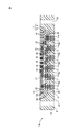
- FIG. 2 is a cross-sectional view of a laminated wiring board 3a mounted on the probe card 1a of FIG.
- a probe card 1a As shown in FIG. 1, a probe card 1a according to this embodiment includes a mother board 2, a laminated wiring board 3a mounted on one main surface of the mother board 2, and one end connected to the laminated wiring board 3a. A plurality of probe pins 5, a probe head 4 that supports each probe pin 5, and a fixture 24 that fixes the probe head 4 and the laminated wiring board 3 a are provided. For example, an electrical inspection of an object to be inspected 50 such as a semiconductor element Used for.
- the mother substrate 2 is formed with a plurality of mounting electrodes 6 on one main surface for mounting the multilayer wiring substrate 3a.
- each mounting electrode 6 is connected to a predetermined external electrode (not shown) by a wiring electrode (not shown) formed inside the mother substrate and a plurality of via conductors (not shown).
- the mother substrate 2 is made of, for example, glass epoxy resin.
- the probe head 4 holding each probe pin 5 and the laminated wiring board 3a are fixed to the mother board by a fixture 24.
- the fixing member 24 of this embodiment has an end portion formed in a flange shape, and a cross section in a direction parallel to the length direction is T-shaped.
- the laminated wiring board 3a includes the core substrate 7, and the side surface and the lower surface 12 of the core substrate 7 (the main surface on the mother substrate 2 side, which corresponds to “the other main surface of the core substrate” in the present invention). And a plurality of metal pins 11 (corresponding to the “columnar conductor” of the present invention) disposed inside the resin portion 8.
- the core substrate 7 includes a ceramic laminated portion 9 disposed on the mother substrate 2 side and a resin laminated portion 10 laminated on the upper surface 13 of the ceramic laminated portion 9 (a main surface opposite to the main surface on the mother substrate 2 side). And have. At this time, the ceramic laminated portion 9 is formed by alternately laminating ceramic layers 9a and wiring layers 9b.
- Each ceramic layer 9a is formed of various ceramics such as a low-temperature co-fired ceramic (LTCC) or a high-temperature fired ceramic (HTCC) mainly composed of a ceramic (for example, alumina) containing borosilicate glass. be able to.
- the ceramic laminated portion 9 is formed of the three ceramic layers 9a and the two wiring layers 9b. However, the number of these layers can be changed as appropriate.
- Each ceramic layer 9a is provided with a plurality of via conductors 15 that connect the wiring electrodes 14 formed in different wiring layers 9b.
- Each wiring electrode 14 and each via conductor 15 are each formed of a metal such as Cu, Ag, or Al.
- the various wiring electrodes 14 formed on each wiring layer 9b are formed by screen printing using a conductive paste containing the metal (Cu, Ag, Al, etc.), for example.
- the resin laminate portion 10 is made of a laminate of a plurality of resin layers 10 a and is laminated on the upper surface 13 of the ceramic laminate portion 9.
- a plurality of connection electrodes 18 to which the probe pins 5 are connected are formed on the upper surface 17 (the main surface opposite to the surface facing the ceramic multilayer portion 9) of the resin multilayer portion 10.
- Each connection electrode 18 can be formed of, for example, a base electrode formed of Cu or the like and a surface electrode obtained by performing Ni / Au plating on the base electrode.
- each wiring electrode 19 forms a Ti film as a base electrode on the main surface of the resin layer 10a by sputtering or the like, and similarly forms a Cu film on the Ti film by sputtering or the like. And it can form by forming a Cu film
- Each wiring electrode 14 formed on the ceramic laminated portion 9 is formed by screen printing or the like and thus has a thick film pattern, whereas each wiring electrode 19 formed on the resin laminated portion 10 is formed by sputtering or the like. Since it is formed into a film, it becomes a thin film pattern. Moreover, each wiring electrode 19 formed in the resin laminated portion 10 is thinned by photolithography.
- connection electrode 18 is electrically connected to a plurality of external electrodes (not shown) formed on the other main surface of the mother substrate 2. Specifically, as shown in FIG. 1 and FIG. 2, each connection electrode 18 is connected to each wiring electrode 19 and each via conductor 20 formed in the resin laminated portion 10 and each formed in the ceramic laminated portion 9. The wiring electrodes 14 and via conductors 15 are connected to predetermined external electrodes (not shown) via wiring electrodes (not shown) and via conductors (not shown) formed on the mother substrate 2.
- the resin portion 8 is disposed so as to cover the side surface and the lower surface 12 of the core substrate 7.
- the core substrate 7 is disposed so as to fit into the recess of the resin portion 8.
- a through hole 22 is formed in the thickness direction of the resin portion 8 in order to pass the fixture 24 that fixes the laminated wiring board 3 a to the mother substrate 2.
- a resin such as an epoxy resin can be used for the resin portion 8.
- the resin portion 8 can be formed by using techniques such as a coating method, a printing method, a transfer mold method, a compression mold method, and the like.
- the surface 21 opposite to the surface of the resin portion 8 facing the core substrate 7 and the mother substrate 2 are connected by soldering or the like.
- a plurality of metal pins 11 are disposed in the resin portion 8 so as to be joined to a plurality of electrodes 23 provided on the lower surface 12 of the core substrate 7 on the mother substrate 2 side.
- the probe pins 5 are electrically connected by the wiring layer 9 b of the core substrate 7.
- Each metal pin 11 can be formed by, for example, shearing a wire formed of a metal such as Cu, Ag, or Al.
- the end surface 11a which is the exposed part of each metal pin 11 in the opposite surface 21 of the resin part 8 may be plated.
- a metal pin is used, but a via conductor or a post electrode formed of a conductive paste or the like may be formed instead of the metal pin.
- the ceramic laminated portion 9 in which the ceramic layers 9a and the wiring layers 9b are alternately laminated is formed, and the resin laminated portion 10 in which the resin layer 10a is laminated is laminated on the upper surface of the ceramic laminated portion 9, and the core substrate 7 Form.
- a plurality of electrodes 23 are provided on the lower surface 12 of the core substrate 7, and the metal pins 11 are erected at the positions of the electrodes 23.
- the side surface and the lower surface 12 of the core substrate 7 are coated with resin and cured to form the resin portion 8.
- the opposite surface 21 of the resin portion 8 is polished in order to locate the metal pin and ensure flatness.
- the through-hole 22 for letting the fixing tool 24 pass in the thickness direction of the resin portion 8 is formed by drilling or laser processing.
- dimension processing is performed by dicing or laser to form the laminated wiring board 3a into a predetermined size.
- the core substrate 7 having the ceramic laminated portion 9 is processed by fixing the laminated wiring substrate 3a to the mother substrate 2 by coating the side surface and the lower surface 12 of the core substrate 7 with resin. 7 can be applied to the resin portion 8 instead. Since the processing to the resin is easier than the processing to the ceramic, it is possible to reduce the occurrence of defects such as chipping when processing the ceramic substrate, and it is possible to regenerate the resin portion.
- the thermal expansion coefficient of this portion can be matched with the thermal expansion coefficient of the mother substrate 2.
- the size of the core substrate 7 can be reduced while keeping the size of the laminated wiring board 3a. Since the ceramic substrate is more expensive than the resin substrate, the number of the ceramic laminates 9 can be increased and the manufacturing cost can be reduced by reducing the ceramic laminated portion 9.
- the resin laminated portion 10 is provided on the core substrate 7, the wiring can be easily thinned, so that it is possible to provide the laminated wiring substrate 3 a that can cope with the electrical inspection of a semiconductor element having a narrow terminal pitch.
- the resin portion 8 and the resin laminate portion 10 are relieved of stress and impact due to physical contact when using the probe card. It can function as a material. Therefore, deformation and breakage of the ceramic laminated portion 9 can be reduced, the durability of the laminated wiring board 3a can be improved, and disconnection of each wiring electrode 14 can be reduced.
- the through hole 22 is provided in the thickness direction of the resin portion 8.
- the through hole may not be provided.
- the laminated wiring board 3a can be fixed to the mother board by a cover body or the like fixed to the mother board 2.
- a hole (bottomed recess) that does not penetrate may be formed.
- the shape of the through hole 22 may be different.
- the through hole 22 has an end surface (cross section) in a direction parallel to the thickness direction of the multilayer wiring board 3a formed in a T shape. If it does in this way, the edge part (flange part) of the fixing tool 24 can be accommodated in the through-hole 22.
- the core substrate 7 may be formed of only the ceramic laminated portion 9.
- the probe pin side of the core substrate 7 also with the ceramic laminated portion 9, flatness can be easily ensured, and distortion and warpage of the laminated wiring substrate 3a due to a load can be reduced.
- FIGS. 5 is a cross-sectional view of the probe card 1b
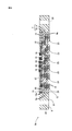
- FIG. 6 is a cross-sectional view of the laminated wiring board 3b mounted on the probe card 1b.
- the laminated wiring board 3b mounted on the probe card 1b according to this embodiment differs from the first embodiment described with reference to FIGS. 1 and 2 in that a core board is provided as shown in FIGS. 7 is not covered with the resin portion 8. Since other configurations are the same as those of the multilayer wiring board 3a of the first embodiment, description thereof is omitted by attaching the same reference numerals.
- the resin portion 8 is disposed so as to cover the side surface of the core substrate 7, and the through hole 22 is formed in the thickness direction of the resin portion 8 in order to pass the fixture 24 that fixes the laminated wiring substrate 3 b to the mother substrate. Is formed.
- a plurality of connection electrodes 18 to which the probe pins 5 are connected are provided on the upper surface 17 of the core substrate 7, and a plurality of electrodes for electrically connecting the mother substrate 2 and the probe pins 5 to the lower surface 12. 23 is provided.
- the core substrate 7 may be formed of only the ceramic laminated portion 9.
- the probe pin side of the core substrate 7 also with the ceramic laminated portion 9, flatness can be easily ensured, and distortion and warping of the laminated wiring substrate 3b due to a load can be reduced.
- the present invention can be widely applied to various probe cards used for electrical inspection of an object to be inspected and laminated wiring boards used for the same.
Landscapes
- Engineering & Computer Science (AREA)
- Microelectronics & Electronic Packaging (AREA)
- Chemical & Material Sciences (AREA)
- Ceramic Engineering (AREA)
- Manufacturing & Machinery (AREA)
- Inorganic Chemistry (AREA)
- Physics & Mathematics (AREA)
- General Physics & Mathematics (AREA)
- Power Engineering (AREA)
- Measuring Leads Or Probes (AREA)
- Testing Or Measuring Of Semiconductors Or The Like (AREA)
- Production Of Multi-Layered Print Wiring Board (AREA)
Abstract
樹脂層の積層体を有するプローブカード用積層配線基板において、セラミック基板を樹脂で被覆することにより、チッピング等の不具合の発生を低減し、製造コストを抑える。 積層配線基板3aは、コア基板7と、コア基板7の側面および下面12を被覆する樹脂部8と、樹脂部8の内部に配設された複数の金属ピン11とを備える。コア基板7は、マザー基板側に配置されたセラミック積層部9と、セラミック積層部9におけるマザー基板と反対側13の主面に積層された樹脂積層部10とを有する。樹脂部8には、複数の金属ピン11が配設され、樹脂部8の厚さ方向に貫通するする貫通孔22が形成される。貫通孔22に固定具24を通すことにより、積層配線基板3aがマザー基板に搭載される。
Description
本発明は、セラミック層を有する積層配線基板およびこの積層配線基板を用いたプローブカードに関する。
従来、半導体素子の電気的な検査に用いられるプローブカードでは、プローブピンとマザー基板の再配線を行うために積層配線基板が用いられる。この種の積層配線基板のなかに、複数のセラミック層が積層されてなるセラミック積層部を有するものがある。
例えば、図8に示すように、特許文献1に記載のセラミック配線基板100は、複数のセラミック絶縁層101aが積層されてなるセラミック層101と、複数の絶縁樹脂層102aが積層されてなる樹脂層102とを備え、セラミック層101上に樹脂層102が積層された構造となる。樹脂層102は、絶縁樹脂層102aと配線層103が交互に積層され、絶縁樹脂層102aの上下に位置する各配線層103間がビア導体104で接続される。また、最下層の絶縁樹脂層102aに形成されたビア導体104と、セラミック配線基板100の上面に露出した内部配線105の端部とが電気的に接続される。
このとき、セラミック層101の上面に、ビア導体104と内部配線105との接続部を離間して取り囲むように凸部109が形成される。凸部109は、絶縁樹脂層102aを形成する樹脂よりもヤング率の大きい材料で形成される。
このような配線基板によれば、ビア導体104と内部配線105の端部との接続部は、周囲を取り囲むヤング率が大きい凸部109によって保護されるため、当該接続部に加わる熱応力が凸部109により低減され、断線の可能性が低減された高信頼性の配線基板となる。
しかしながら、セラミック基板は加工が困難であるため、例えば、プローブカード用のセラミック基板の寸法加工を施す際に、チッピング等の不具合が発生することがある。この種のセラミック基板は、数mm程度の厚さが必要な場合があるが、セラミック基板の厚さが増すとさらに加工時の不具合のリスクが高くなってしまう。また、寸法加工は最終工程に近いため、この工程で加工不具合が発生すると修復が難しいという問題もある。
本発明は、上記した課題に鑑みてなされたものであり、セラミック層を有するコア基板を備えるプローブカード用の積層配線基板において、コア基板の側面を樹脂で被覆することにより、外形加工や穴あけ加工時のチッピング等の不具合の発生を低減することを目的とする。
上記した目的を達成するために、本発明のプローブカード用積層配線基板は、複数のプローブピンが接続されるプローブカード用積層配線基板において、複数のセラミック層が積層されてなるセラミック積層部を有し、一方主面に前記複数のプローブピンが接続されるコア基板と、前記コア基板の側面を被覆するように配置された樹脂部とを備えることを特徴とする。
この構成によると、コア基板の側面を樹脂で被覆することにより、穴あけや外形カット等の加工を、コア基板ではなく樹脂部に施すことができるため、コア基板を加工する場合に問題となるチッピング等の不具合の発生を低減することができる。また、加工不具合が発生しても、樹脂の場合はやり直しが容易である。また、コア基板の側面を樹脂部で被覆することにより、積層配線基板のサイズは変えずに、コア基板のサイズを小さくすることができるため、製造コストを抑えることが可能である。
また、前記コア基板は、前記樹脂部は、前記コア基板の他方主面をさらに被覆し、前記樹脂部における前記コア基板の前記他方主面を被覆する部分に配設され、前記複数のプローブピンと電気的に接続され、一方の端面が前記樹脂部における前記コア基板の前記他方主面と対向する面に露出する柱状導体とをさらに備えていてもよい。
この場合、プローブカード用積層配線基板のマザー基板側の面を樹脂で覆うことにより、マザー基板の熱膨張係数に近づけることができる。また、プローブパッド側の面をセラミック基板とすることにより、半導体ウェハの熱膨張係数に近づけることができる。このため、プローブカードによる検査時の熱によって、積層配線基板の反りや歪みを低減することができる。さらに、プローブカード用積層配線基板として重要な基板の平坦性も、樹脂部を研磨することにより容易に確保することができる。また、コア基板の他方主面を被覆する部分に、コア基板の一部の配線を形成すると、コア基板をさらに小さくできるため、製造コストを抑えることができる。
また、前記樹脂部における前記コア基板の前記側面を被覆する部分には、厚み方向に凹んだ穴部が形成されていてもよい。プローブカード用積層配線基板は、プローブヘッドを組みつけたり積層配線基板をマザー基板に固定したりするために、穴あけ加工を施す場合があるが、樹脂部に穴部を設けることで、コア基板への加工が不要になり、チッピング等の不具合を防止することができる。ここで、穴部は樹脂部を貫通していてもよい。
また、前記コア基板は、前記セラミック積層部における前記樹脂部側の面と対向する面に積層された樹脂積層部をさらに備え、前記樹脂積層部において、前記樹脂部側の面と対向する面が、前記コア基板の前記一方主面をなしていてもよい。この場合、例えば、樹脂積層部を微細な配線が可能なポリイミドなどの樹脂で形成することで、配線の細線化が容易になる。また、プローブカードは検査対象の半導体素子に何度も接触させるので、セラミック積層部に樹脂積層部を積層することで、その応力や衝撃を緩和させることができるため、積層配線基板の変形を防止することができる。
また、上記の積層配線基板を、被検査物の電気検査を行うプローブカードに使用するのが好ましい。こうすると、耐久性が高く、かつ、マザー基板との接続信頼性の高いプローブカードを提供することができる。
本発明によれば、セラミック基板を樹脂部で被覆してプローブカード用積層配線基板を構成することで、穴あけや外形カット等の加工をセラミック基板ではなく樹脂部に施すことができるため、セラミック基板を加工する場合のチッピング等の製造リスクを避け、再生可能な樹脂とするとともに、セラミック基板のサイズを小さくすることができるため、積層配線基板の製造コストを抑えることが可能である。
<第1実施形態>
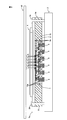
本発明の一実施形態にかかるプローブカード1aについて、図1、図2を参照して説明する。なお、図1はプローブカード1aの断面図、図2は図1のプローブカード1aに搭載される積層配線基板3aの断面図である。
本発明の一実施形態にかかるプローブカード1aについて、図1、図2を参照して説明する。なお、図1はプローブカード1aの断面図、図2は図1のプローブカード1aに搭載される積層配線基板3aの断面図である。
この実施形態にかかるプローブカード1aは、図1に示すように、マザー基板2と、該マザー基板2の一方主面に実装された積層配線基板3aと、一端が積層配線基板3aに接続される複数のプローブピン5と、各プローブピン5を支持するプローブヘッド4と、プローブヘッド4および積層配線基板3aを固定する固定具24とを備え、例えば、半導体素子などの被検査物50の電気検査に使用される。
マザー基板2は、一方主面に積層配線基板3aを実装するための複数の実装電極6が形成される。ここで、各実装電極6は、マザー基板の内部に形成された配線電極(図示省略)や複数のビア導体(図示省略)により所定の外部電極(図示省略)に接続される。マザー基板2は、例えば、ガラスエポキシ樹脂などで形成されている。なお、各プローブピン5を保持するプローブヘッド4および、積層配線基板3aは、固定具24によりマザー基板に固定される。この実施形態の固定具24は、端部がフランジ状に形成され、長さ方向と平行な方向の断面がT字状になっている。
図2に示すように、積層配線基板3aは、コア基板7と、コア基板7の側面および下面12(マザー基板2側の主面、本発明における「コア基板の他方主面」に相当する)を被覆する樹脂部8と、樹脂部8の内部に配設された複数の金属ピン11(本発明の「柱状導体」に相当する)とを備える。コア基板7は、マザー基板2側に配置されたセラミック積層部9と、該セラミック積層部9の上面13(マザー基板2側の主面と反対側の主面)に積層された樹脂積層部10とを有する。このとき、セラミック積層部9は、セラミック層9aと配線層9bが交互に積層されて形成される。なお、各セラミック層9aは、例えば、ホウケイ酸系ガラスを含有するセラミック(たとえば、アルミナ)を主成分とする低温同時焼成セラミック(LTCC)、高温焼成セラミック(HTCC)など、種々のセラミックで形成することができる。また、この実施形態では、セラミック積層部9が、3つのセラミック層9aと2つの配線層9bとで形成されているが、これらの層数は適宜変更することができる。
セラミック積層部9の各配線層9bには、各種配線電極14が形成されている。また、各セラミック層9aには、異なる配線層9bに形成された配線電極14同士を接続する複数のビア導体15が形成される。各配線電極14および各ビア導体15はそれぞれ、Cu、Ag、Al等の金属で形成される。各配線層9bに形成される各種配線電極14は、例えば、上記金属(Cu、Ag、Al等)を含有する導電性ペーストを用いたスクリーン印刷などで形成される。
樹脂積層部10は、複数の樹脂層10aの積層体からなり、セラミック積層部9の上面13に積層される。ここで、樹脂積層部10の上面17(セラミック積層部9との対向面と反対側の主面)には、各プローブピン5が接続される複数の接続電極18が形成される。なお、各接続電極18は、例えば、Cu等で形成された下地電極と、該下地電極上にNi/Auめっきが施されてなる表面電極とでそれぞれ形成することができる。
各樹脂層10aには、各種配線電極19および複数のビア導体20が形成される。この場合、各配線電極19は、例えば、樹脂層10aの主面に、下地電極としてのTi膜をスパッタ等により成膜し、同じくスパッタ等によりTi膜上にCu膜を成膜する。そして、Cu膜上に、電解または無電解めっきにより、同じくCu膜を成膜することで形成することができる。なお、セラミック積層部9に形成された各配線電極14は、スクリーン印刷などで形成されるため厚膜パターンとなるのに対して、樹脂積層部10に形成された各配線電極19は、スパッタ等で成膜されるため薄膜パターンとなる。また、樹脂積層部10に形成された各配線電極19は、フォトリソグラフィ加工で細線化される。
各接続電極18は、マザー基板2の他方主面に形成された複数の外部電極(図示省略)にそれぞれ電気的に接続される。具体的には、図1および図2に示すように、各接続電極18は、それぞれ、樹脂積層部10に形成された各配線電極19および各ビア導体20、セラミック積層部9に形成された各配線電極14および各ビア導体15、マザー基板2に形成された配線電極(図示省略)およびビア導体(図示省略)等を介して所定の各外部電極(図示省略)に接続される。
樹脂部8は、コア基板7の側面および下面12を被覆するように配置される。換言すると、コア基板7は、樹脂部8の凹部に嵌合して配置される。このように樹脂部8を形成することで、積層配線基板3aとして必要な大きさを確保しつつ、コア基板7のサイズを小さくすることができる。さらに、積層配線基板3aをマザー基板2に固定する固定具24を通すために、樹脂部8の厚み方向に貫通孔22(本発明における「穴部」に相当する)が形成されている。
樹脂部8には、例えばエポキシ樹脂などの樹脂を使用することができる。また、樹脂部8の形成には、塗布方式、印刷方式、トランスファモールド方式、コンプレッションモールド方式などの技術を用いることができる。樹脂部8のコア基板7との対向面の反対面21とマザー基板2とは、半田などにより接続される。
複数の金属ピン11(本発明の「柱状導体」に相当する)は、コア基板7のマザー基板2側の下面12に設けられた複数の電極23に接合するように樹脂部8に配設され、コア基板7の配線層9bにより各プローブピン5と電気的に接続される。各金属ピン11は、例えば、Cu、Ag、Al等の金属で形成された線材をせん断加工するなどして形成することができる。また、樹脂部8の反対面21における各金属ピン11の露出部分である端面11aにはめっき処理が施されていてもよい。なお、本実施形態では金属ピンを使用しているが、金属ピンの代わりに、導電性ペースト等で形成されるビア導体、もしくはポスト電極を形成してもよい。
ここで、積層配線基板3aの製造方法を簡単に説明する。まず、セラミック層9aと配線層9bが交互に積層されたセラミック積層部9を形成し、セラミック積層部9の上面に、樹脂層10aが積層された樹脂積層部10を積層して、コア基板7を形成する。コア基板7の下面12には、複数の電極23を設け、電極23の位置に金属ピン11を立設する。その後、コア基板7の側面および下面12を樹脂で被覆し、硬化して、樹脂部8を形成する。樹脂部8を形成した後、金属ピンの頭出しと平坦性の確保のために、樹脂部8の反対面21を研磨する。また、樹脂部8の厚み方向に、固定具24を通すための貫通孔22をドリル加工やレーザー加工により形成する。最後に、ダイシングまたはレーザーにより寸法加工を行い、積層配線基板3aを所定のサイズに成形する。
したがって、上記した実施形態によれば、コア基板7の側面および下面12を樹脂で被覆することにより、マザー基板2へ積層配線基板3aを固定するための加工を、セラミック積層部9を有するコア基板7ではなく、樹脂部8に施すことができる。樹脂への加工はセラミックへの加工より容易であるため、セラミック基板を加工する際のチッピング等の不具合の発生を低減することができ、さらには樹脂部を再生することが可能になる。
また、積層配線基板3aにおけるマザー基板2側の面は樹脂部8で覆われているため、この部分の熱膨張係数をマザー基板2の熱膨張係数に合わせることが可能である。熱膨張係数を合わせることで、検査時の熱による積層配線基板3aの反りや歪みの発生を低減することができる。
また、樹脂部8を設けることにより、積層配線基板3aのサイズはそのままで、コア基板7のサイズを小さくすることができる。セラミック基板は樹脂基板よりも高価であるため、セラミック積層部9を小さくすることで、その取り個数を増やすことができ、製造コストを抑えることができる。
さらに、コア基板7に樹脂積層部10を設けることで、配線の細線化が容易になるため、端子ピッチが狭い半導体素子の電気検査に対応可能な積層配線基板3aを提供することができる。また、セラミック積層部9の下面12、上面13に樹脂部8および樹脂積層部10を積層することで、樹脂部8および樹脂積層部10をプローブカード使用時の物理的接触による応力や衝撃を緩和する材料として機能させることができる。したがって、セラミック積層部9の変形や破損を低減し、積層配線基板3aの耐久性の向上を図ることができるとともに、各配線電極14の断線を低減することができる。
(積層配線基板の変形例)
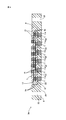
上記した実施形態では、樹脂部8の厚み方向に貫通孔22を設けているが、図3(a)に示すように、貫通孔は設けなくてもよい。この場合は、マザー基板2に固定されたカバー体等により積層配線基板3aをマザー基板に固定することができる。また、この構成において、例えばプローブヘッド4を積層配線基板3aに固定することを目的として、貫通していない穴部(有底凹部)が形成されていてもよい。
上記した実施形態では、樹脂部8の厚み方向に貫通孔22を設けているが、図3(a)に示すように、貫通孔は設けなくてもよい。この場合は、マザー基板2に固定されたカバー体等により積層配線基板3aをマザー基板に固定することができる。また、この構成において、例えばプローブヘッド4を積層配線基板3aに固定することを目的として、貫通していない穴部(有底凹部)が形成されていてもよい。
また、図3(b)のように、貫通孔22の形状が異なっていても構わない。この場合、貫通孔22は、積層配線基板3aの厚み方向と平行な方向の端面(横断面)がT字状に形成される。このようにすると、固定具24の端部(フランジ部)を、貫通孔22に収納することができる。
また、図4に示すように、上述の積層配線基板3aにおいて、コア基板7がセラミック積層部9だけで形成されていてもよい。コア基板7のプローブピン側もセラミック積層部9で形成することにより、容易に平坦性を確保することができ、また、荷重による積層配線基板3aの歪みや反りを低減することができる。
<第2実施形態>
本発明の第2実施形態にかかるプローブカード1bについて、図5、図6を参照して説明する。なお、図5はプローブカード1bの断面図、図6はプローブカード1bに搭載される積層配線基板3bの断面図である。
本発明の第2実施形態にかかるプローブカード1bについて、図5、図6を参照して説明する。なお、図5はプローブカード1bの断面図、図6はプローブカード1bに搭載される積層配線基板3bの断面図である。
この実施形態にかかるプローブカード1bに搭載される積層配線基板3bが、図1、図2を参照して説明した第1実施形態と異なるところは、図5、図6に示すように、コア基板7の下面12が樹脂部8で被覆されていないことである。その他の構成は第1実施形態の積層配線基板3aと同じであるため同一符号を付すことにより説明を省略する。
この場合、樹脂部8は、コア基板7の側面を被覆するように配置され、積層配線基板3bをマザー基板に固定する固定具24を通すために、樹脂部8の厚み方向に貫通孔22が形成されている。コア基板7の上面17には、各プローブピン5が接続される複数の接続電極18が設けられるとともに、下面12には、マザー基板2とプローブピン5を電気的に接続するための複数の電極23が設けられる。
この実施形態によれば、第1実施形態と同様の効果を得ることができる。
(積層配線基板の変形例)
図7に示すように、上述の積層配線基板3bにおいて、コア基板7がセラミック積層部9だけで形成されていてもよい。コア基板7のプローブピン側もセラミック積層部9で形成することにより、容易に平坦性を確保することができ、また、荷重による積層配線基板3bの歪みや反りを低減することができる。
図7に示すように、上述の積層配線基板3bにおいて、コア基板7がセラミック積層部9だけで形成されていてもよい。コア基板7のプローブピン側もセラミック積層部9で形成することにより、容易に平坦性を確保することができ、また、荷重による積層配線基板3bの歪みや反りを低減することができる。
なお、本発明は上記した各実施形態に限定されるものではなく、その趣旨を逸脱しない限りにおいて、上記したもの以外に種々の変更を行なうことが可能である。例えば、各実施形態及び変形例の構成を組み合わせてもよい。
本発明は、被検査物の電気検査に使用される種々のプローブカードおよびこれに用いられる積層配線基板に広く適用することができる。
1a、1b プローブカード
3a、3b 積層配線基板
5 プローブピン
7 コア基板
8 樹脂部
9 セラミック積層部
9a セラミック層
10 樹脂積層部
10a 樹脂層
11 金属ピン(柱状導体)
22 貫通孔(穴部)
3a、3b 積層配線基板
5 プローブピン
7 コア基板
8 樹脂部
9 セラミック積層部
9a セラミック層
10 樹脂積層部
10a 樹脂層
11 金属ピン(柱状導体)
22 貫通孔(穴部)
Claims (5)
- 複数のプローブピンが接続されるプローブカード用積層配線基板において、
複数のセラミック層が積層されてなるセラミック積層部を有し、一方主面に前記複数のプローブピンが接続されるコア基板と、
前記コア基板の側面を被覆するように配置された樹脂部と
を備えることを特徴とするプローブカード用積層配線基板。 - 前記樹脂部は、前記コア基板の他方主面をさらに被覆し、
前記樹脂部における前記コア基板の前記他方主面を被覆する部分に配設され、前記複数のプローブピンと電気的に接続され、一方の端面が前記樹脂部における前記コア基板の前記他方主面と対向する面に露出する柱状導体とをさらに備えることを特徴とする請求項1に記載のプローブカード用積層配線基板。 - 前記樹脂部における前記コア基板の前記側面を被覆する部分には、厚み方向に凹んだ穴部が形成されていることを特徴とする請求項1または2に記載のプローブカード用積層配線基板。
- 前記コア基板は、前記セラミック積層部における前記樹脂部側の面と対向する面に積層された樹脂積層部をさらに備え、
前記樹脂積層部において、前記樹脂部側の面と対向する面が、前記コア基板の前記一方主面をなすことを特徴とする請求項1ないし3のいずれかに記載のプローブカード用積層配線基板。 - 請求項1ないし4のいずれかに記載のプローブカード用積層配線基板を備え、被検査物の電気検査を行うことを特徴とするプローブカード。
Priority Applications (3)
| Application Number | Priority Date | Filing Date | Title |
|---|---|---|---|
| CN201780014320.4A CN108713354B (zh) | 2016-03-03 | 2017-02-20 | 探针卡用层叠布线基板以及具备它的探针卡 |
| JP2018503036A JP6508416B2 (ja) | 2016-03-03 | 2017-02-20 | プローブカード用積層配線基板およびこれを備えるプローブカード |
| US16/114,458 US11067600B2 (en) | 2016-03-03 | 2018-08-28 | Multilayer circuit board used for probe card and probe card including multilayer circuit board |
Applications Claiming Priority (2)
| Application Number | Priority Date | Filing Date | Title |
|---|---|---|---|
| JP2016-040950 | 2016-03-03 | ||
| JP2016040950 | 2016-03-03 |
Related Child Applications (1)
| Application Number | Title | Priority Date | Filing Date |
|---|---|---|---|
| US16/114,458 Continuation US11067600B2 (en) | 2016-03-03 | 2018-08-28 | Multilayer circuit board used for probe card and probe card including multilayer circuit board |
Publications (1)
| Publication Number | Publication Date |
|---|---|
| WO2017150232A1 true WO2017150232A1 (ja) | 2017-09-08 |
Family
ID=59743792
Family Applications (1)
| Application Number | Title | Priority Date | Filing Date |
|---|---|---|---|
| PCT/JP2017/006049 Ceased WO2017150232A1 (ja) | 2016-03-03 | 2017-02-20 | プローブカード用積層配線基板およびこれを備えるプローブカード |
Country Status (4)
| Country | Link |
|---|---|
| US (1) | US11067600B2 (ja) |
| JP (1) | JP6508416B2 (ja) |
| CN (1) | CN108713354B (ja) |
| WO (1) | WO2017150232A1 (ja) |
Cited By (2)
| Publication number | Priority date | Publication date | Assignee | Title |
|---|---|---|---|---|
| JP2021071472A (ja) * | 2019-10-30 | 2021-05-06 | 巨擘科技股▲ふん▼有限公司Princo Corp. | プローブカード装置 |
| WO2026070459A1 (ja) * | 2024-09-30 | 2026-04-02 | 京セラ株式会社 | 複合配線基板および電子モジュール |
Families Citing this family (8)
| Publication number | Priority date | Publication date | Assignee | Title |
|---|---|---|---|---|
| TWI632376B (zh) * | 2016-05-31 | 2018-08-11 | 巨擘科技股份有限公司 | 探針卡裝置 |
| KR102652266B1 (ko) * | 2019-01-31 | 2024-03-28 | (주)포인트엔지니어링 | 다층 배선 기판 및 이를 포함하는 프로브 카드 |
| JP7587574B2 (ja) * | 2020-05-07 | 2024-11-20 | 株式会社村田製作所 | 多層基板モジュール |
| TWI815262B (zh) | 2021-12-28 | 2023-09-11 | 財團法人工業技術研究院 | 三維電路板及其製作方法以及探針卡 |
| TWI798027B (zh) | 2022-03-14 | 2023-04-01 | 巨擘科技股份有限公司 | 探針卡裝置 |
| TWI838772B (zh) | 2022-06-20 | 2024-04-11 | 財團法人工業技術研究院 | 低熔點合金複材與複材結構 |
| CN116811040B (zh) * | 2023-08-26 | 2023-11-10 | 江苏鹏利芝达恩半导体有限公司 | 用于制造立式探针卡的陶瓷棒制造方法、设备及存储介质 |
| CN119024023A (zh) * | 2024-09-11 | 2024-11-26 | 特源微测试技术(苏州)有限公司 | 一种高性能低成本的射频探卡及其制造方法 |
Citations (6)
| Publication number | Priority date | Publication date | Assignee | Title |
|---|---|---|---|---|
| JP2000299559A (ja) * | 1999-04-12 | 2000-10-24 | Fujitsu Ten Ltd | パワーモジュール用基板 |
| JP2004228103A (ja) * | 2003-01-17 | 2004-08-12 | Ngk Spark Plug Co Ltd | 配線基板 |
| JP2007019198A (ja) * | 2005-07-07 | 2007-01-25 | Fujitsu Ltd | 積層基板および該積層基板を有する電子機器 |
| JP2009222597A (ja) * | 2008-03-17 | 2009-10-01 | Ngk Spark Plug Co Ltd | 電気特性測定用配線基板、及び電気特性測定用配線基板の製造方法 |
| US20100117673A1 (en) * | 2008-11-11 | 2010-05-13 | Samsung Electronics Co., Ltd. | Interface structure of wafer test equipment |
| JP2011228427A (ja) * | 2010-04-19 | 2011-11-10 | Kyocera Corp | プローブカードおよびプローブ装置 |
Family Cites Families (15)
| Publication number | Priority date | Publication date | Assignee | Title |
|---|---|---|---|---|
| US6936917B2 (en) * | 2001-09-26 | 2005-08-30 | Molex Incorporated | Power delivery connector for integrated circuits utilizing integrated capacitors |
| US7102367B2 (en) * | 2002-07-23 | 2006-09-05 | Fujitsu Limited | Probe card and testing method of semiconductor chip, capacitor and manufacturing method thereof |
| US7501839B2 (en) * | 2005-04-21 | 2009-03-10 | Endicott Interconnect Technologies, Inc. | Interposer and test assembly for testing electronic devices |
| TWI271525B (en) * | 2006-01-17 | 2007-01-21 | Chipmos Technologies Inc | Probe head with vertical probes, method for manufacturing the probe head, and probe card using the probe head |
| JP5236379B2 (ja) * | 2007-08-24 | 2013-07-17 | 日本特殊陶業株式会社 | Ic検査装置用基板及びその製造方法 |
| CN201188722Y (zh) * | 2008-04-30 | 2009-01-28 | 深圳市兴森快捷电路科技股份有限公司 | 印制线路板及其连接结构 |
| JP5550280B2 (ja) * | 2009-07-29 | 2014-07-16 | 京セラ株式会社 | 多層配線基板 |
| JP5383447B2 (ja) | 2009-11-20 | 2014-01-08 | 京セラ株式会社 | 配線基板およびプローブカードならびに電子装置 |
| KR101089936B1 (ko) * | 2010-01-13 | 2011-12-05 | 삼성전기주식회사 | 다층 세라믹 회로 기판 및 제조방법 |
| JP5563917B2 (ja) * | 2010-07-22 | 2014-07-30 | セミコンダクター・コンポーネンツ・インダストリーズ・リミテッド・ライアビリティ・カンパニー | 回路装置及びその製造方法 |
| WO2013031822A1 (ja) * | 2011-08-29 | 2013-03-07 | 京セラ株式会社 | 薄膜配線基板およびプローブカード用基板 |
| JP2013077751A (ja) * | 2011-09-30 | 2013-04-25 | Dainippon Printing Co Ltd | コネクタ接続用配線基板、コネクタ接続用配線基板の製造方法、及び基板/配線基板の接続構造 |
| CN103891425B (zh) * | 2011-10-21 | 2017-06-13 | 株式会社村田制作所 | 多层布线基板、探针卡以及多层布线基板的制造方法 |
| CN203661413U (zh) * | 2013-11-26 | 2014-06-18 | 洛阳隆盛科技有限责任公司 | 一种阶梯式印制板 |
| JPWO2016024534A1 (ja) * | 2014-08-11 | 2017-05-25 | 株式会社村田製作所 | プローブカードおよびこのプローブカードが備える積層配線基板 |
-
2017
- 2017-02-20 CN CN201780014320.4A patent/CN108713354B/zh active Active
- 2017-02-20 JP JP2018503036A patent/JP6508416B2/ja active Active
- 2017-02-20 WO PCT/JP2017/006049 patent/WO2017150232A1/ja not_active Ceased
-
2018
- 2018-08-28 US US16/114,458 patent/US11067600B2/en active Active
Patent Citations (6)
| Publication number | Priority date | Publication date | Assignee | Title |
|---|---|---|---|---|
| JP2000299559A (ja) * | 1999-04-12 | 2000-10-24 | Fujitsu Ten Ltd | パワーモジュール用基板 |
| JP2004228103A (ja) * | 2003-01-17 | 2004-08-12 | Ngk Spark Plug Co Ltd | 配線基板 |
| JP2007019198A (ja) * | 2005-07-07 | 2007-01-25 | Fujitsu Ltd | 積層基板および該積層基板を有する電子機器 |
| JP2009222597A (ja) * | 2008-03-17 | 2009-10-01 | Ngk Spark Plug Co Ltd | 電気特性測定用配線基板、及び電気特性測定用配線基板の製造方法 |
| US20100117673A1 (en) * | 2008-11-11 | 2010-05-13 | Samsung Electronics Co., Ltd. | Interface structure of wafer test equipment |
| JP2011228427A (ja) * | 2010-04-19 | 2011-11-10 | Kyocera Corp | プローブカードおよびプローブ装置 |
Cited By (3)
| Publication number | Priority date | Publication date | Assignee | Title |
|---|---|---|---|---|
| JP2021071472A (ja) * | 2019-10-30 | 2021-05-06 | 巨擘科技股▲ふん▼有限公司Princo Corp. | プローブカード装置 |
| US12379399B2 (en) | 2019-10-30 | 2025-08-05 | Princo Corp. | Probe card device |
| WO2026070459A1 (ja) * | 2024-09-30 | 2026-04-02 | 京セラ株式会社 | 複合配線基板および電子モジュール |
Also Published As
| Publication number | Publication date |
|---|---|
| JPWO2017150232A1 (ja) | 2018-08-30 |
| JP6508416B2 (ja) | 2019-05-08 |
| CN108713354A (zh) | 2018-10-26 |
| CN108713354B (zh) | 2020-12-11 |
| US20180364280A1 (en) | 2018-12-20 |
| US11067600B2 (en) | 2021-07-20 |
Similar Documents
| Publication | Publication Date | Title |
|---|---|---|
| JP6508416B2 (ja) | プローブカード用積層配線基板およびこれを備えるプローブカード | |
| JP4473807B2 (ja) | 積層半導体装置及び積層半導体装置の下層モジュール | |
| JP5485110B2 (ja) | 配線基板及びその製造方法、電子装置 | |
| JP6323768B1 (ja) | 貫通電極基板及びその製造方法、並びに実装基板 | |
| JP6304263B2 (ja) | 積層配線基板およびこれを備える検査装置 | |
| JPWO2015102107A1 (ja) | 積層配線基板およびこれを備える検査装置 | |
| US9374889B2 (en) | Interposer and electronic component package | |
| US20120319289A1 (en) | Semiconductor package | |
| WO2015151809A1 (ja) | 積層配線基板およびこれを備えるプローブカード | |
| US10887991B2 (en) | Wiring substrate for inspection apparatus | |
| JP6589990B2 (ja) | プローブカード用積層配線基板およびこれを備えるプローブカード | |
| JPWO2010027075A1 (ja) | 配線基板およびプローブカード | |
| JPH0763786A (ja) | プローブ構造 | |
| JP5145089B2 (ja) | 電気特性測定用配線基板、及び電気特性測定用配線基板の製造方法 | |
| JP6392630B2 (ja) | 回路基板および回路装置 | |
| US9837345B2 (en) | Interposer and circuit substrate | |
| KR102698002B1 (ko) | 프로브 카드 및 이의 제조 방법 | |
| JP2015002263A (ja) | 配線基板、多層配線基板の製造方法 | |
| JP4789675B2 (ja) | 貫通孔を有する配線基板、その製造方法、ならびに該配線基板を有するプローブカード。 | |
| WO2016114170A1 (ja) | プローブカードおよびこのプローブカードが備える積層配線基板 | |
| JP2006275579A (ja) | 検査基板および検査装置 | |
| JP2008135574A (ja) | 配線基板およびそれを用いた半導体装置とプローブカード | |
| WO2016204209A1 (ja) | 積層配線基板およびこれを備えるプローブカード | |
| JP2017028233A (ja) | インターポーザと回路基板 | |
| JP2007047011A (ja) | 半導体素子検査用基板およびその製造方法 |
Legal Events
| Date | Code | Title | Description |
|---|---|---|---|
| ENP | Entry into the national phase |
Ref document number: 2018503036 Country of ref document: JP Kind code of ref document: A |
|
| NENP | Non-entry into the national phase |
Ref country code: DE |
|
| 121 | Ep: the epo has been informed by wipo that ep was designated in this application |
Ref document number: 17759700 Country of ref document: EP Kind code of ref document: A1 |
|
| 122 | Ep: pct application non-entry in european phase |
Ref document number: 17759700 Country of ref document: EP Kind code of ref document: A1 |