WO2017149958A1 - 有機光電変換素子、二次元センサ、画像センサ及び撮像装置 - Google Patents
有機光電変換素子、二次元センサ、画像センサ及び撮像装置 Download PDFInfo
- Publication number
- WO2017149958A1 WO2017149958A1 PCT/JP2017/001226 JP2017001226W WO2017149958A1 WO 2017149958 A1 WO2017149958 A1 WO 2017149958A1 JP 2017001226 W JP2017001226 W JP 2017001226W WO 2017149958 A1 WO2017149958 A1 WO 2017149958A1
- Authority
- WO
- WIPO (PCT)
- Prior art keywords
- group
- photoelectric conversion
- organic photoelectric
- compound
- organic
- Prior art date
- Legal status (The legal status is an assumption and is not a legal conclusion. Google has not performed a legal analysis and makes no representation as to the accuracy of the status listed.)
- Ceased
Links
- 0 CC*IN(C)** Chemical compound CC*IN(C)** 0.000 description 2
Images


Classifications
-
- C—CHEMISTRY; METALLURGY
- C07—ORGANIC CHEMISTRY
- C07C—ACYCLIC OR CARBOCYCLIC COMPOUNDS
- C07C211/00—Compounds containing amino groups bound to a carbon skeleton
- C07C211/43—Compounds containing amino groups bound to a carbon skeleton having amino groups bound to carbon atoms of six-membered aromatic rings of the carbon skeleton
- C07C211/57—Compounds containing amino groups bound to a carbon skeleton having amino groups bound to carbon atoms of six-membered aromatic rings of the carbon skeleton having amino groups bound to carbon atoms of six-membered aromatic rings being part of condensed ring systems of the carbon skeleton
- C07C211/61—Compounds containing amino groups bound to a carbon skeleton having amino groups bound to carbon atoms of six-membered aromatic rings of the carbon skeleton having amino groups bound to carbon atoms of six-membered aromatic rings being part of condensed ring systems of the carbon skeleton with at least one of the condensed ring systems formed by three or more rings
-
- C—CHEMISTRY; METALLURGY
- C07—ORGANIC CHEMISTRY
- C07C—ACYCLIC OR CARBOCYCLIC COMPOUNDS
- C07C255/00—Carboxylic acid nitriles
- C07C255/01—Carboxylic acid nitriles having cyano groups bound to acyclic carbon atoms
- C07C255/32—Carboxylic acid nitriles having cyano groups bound to acyclic carbon atoms having cyano groups bound to acyclic carbon atoms of a carbon skeleton containing at least one six-membered aromatic ring
- C07C255/42—Carboxylic acid nitriles having cyano groups bound to acyclic carbon atoms having cyano groups bound to acyclic carbon atoms of a carbon skeleton containing at least one six-membered aromatic ring the carbon skeleton being further substituted by singly-bound nitrogen atoms, not being further bound to other hetero atoms
-
- H—ELECTRICITY
- H04—ELECTRIC COMMUNICATION TECHNIQUE
- H04N—PICTORIAL COMMUNICATION, e.g. TELEVISION
- H04N25/00—Circuitry of solid-state image sensors [SSIS]; Control thereof
- H04N25/70—SSIS architectures; Circuits associated therewith
- H04N25/79—Arrangements of circuitry being divided between different or multiple substrates, chips or circuit boards, e.g. stacked image sensors
-
- H—ELECTRICITY
- H10—SEMICONDUCTOR DEVICES; ELECTRIC SOLID-STATE DEVICES NOT OTHERWISE PROVIDED FOR
- H10K—ORGANIC ELECTRIC SOLID-STATE DEVICES
- H10K30/00—Organic devices sensitive to infrared radiation, light, electromagnetic radiation of shorter wavelength or corpuscular radiation
-
- H—ELECTRICITY
- H10—SEMICONDUCTOR DEVICES; ELECTRIC SOLID-STATE DEVICES NOT OTHERWISE PROVIDED FOR
- H10K—ORGANIC ELECTRIC SOLID-STATE DEVICES
- H10K85/00—Organic materials used in the body or electrodes of devices covered by this subclass
- H10K85/20—Carbon compounds, e.g. carbon nanotubes or fullerenes
- H10K85/211—Fullerenes, e.g. C60
-
- H—ELECTRICITY
- H10—SEMICONDUCTOR DEVICES; ELECTRIC SOLID-STATE DEVICES NOT OTHERWISE PROVIDED FOR
- H10K—ORGANIC ELECTRIC SOLID-STATE DEVICES
- H10K85/00—Organic materials used in the body or electrodes of devices covered by this subclass
- H10K85/60—Organic compounds having low molecular weight
- H10K85/631—Amine compounds having at least two aryl rest on at least one amine-nitrogen atom, e.g. triphenylamine
- H10K85/633—Amine compounds having at least two aryl rest on at least one amine-nitrogen atom, e.g. triphenylamine comprising polycyclic condensed aromatic hydrocarbons as substituents on the nitrogen atom
-
- H—ELECTRICITY
- H10—SEMICONDUCTOR DEVICES; ELECTRIC SOLID-STATE DEVICES NOT OTHERWISE PROVIDED FOR
- H10K—ORGANIC ELECTRIC SOLID-STATE DEVICES
- H10K85/00—Organic materials used in the body or electrodes of devices covered by this subclass
- H10K85/60—Organic compounds having low molecular weight
- H10K85/631—Amine compounds having at least two aryl rest on at least one amine-nitrogen atom, e.g. triphenylamine
- H10K85/636—Amine compounds having at least two aryl rest on at least one amine-nitrogen atom, e.g. triphenylamine comprising heteroaromatic hydrocarbons as substituents on the nitrogen atom
-
- C—CHEMISTRY; METALLURGY
- C07—ORGANIC CHEMISTRY
- C07C—ACYCLIC OR CARBOCYCLIC COMPOUNDS
- C07C2602/00—Systems containing two condensed rings
- C07C2602/02—Systems containing two condensed rings the rings having only two atoms in common
- C07C2602/04—One of the condensed rings being a six-membered aromatic ring
- C07C2602/08—One of the condensed rings being a six-membered aromatic ring the other ring being five-membered, e.g. indane
-
- H—ELECTRICITY
- H10—SEMICONDUCTOR DEVICES; ELECTRIC SOLID-STATE DEVICES NOT OTHERWISE PROVIDED FOR
- H10K—ORGANIC ELECTRIC SOLID-STATE DEVICES
- H10K39/00—Integrated devices, or assemblies of multiple devices, comprising at least one organic radiation-sensitive element covered by group H10K30/00
- H10K39/30—Devices controlled by radiation
- H10K39/32—Organic image sensors
-
- H—ELECTRICITY
- H10—SEMICONDUCTOR DEVICES; ELECTRIC SOLID-STATE DEVICES NOT OTHERWISE PROVIDED FOR
- H10K—ORGANIC ELECTRIC SOLID-STATE DEVICES
- H10K85/00—Organic materials used in the body or electrodes of devices covered by this subclass
- H10K85/20—Carbon compounds, e.g. carbon nanotubes or fullerenes
- H10K85/211—Fullerenes, e.g. C60
- H10K85/215—Fullerenes, e.g. C60 comprising substituents, e.g. PCBM
-
- H—ELECTRICITY
- H10—SEMICONDUCTOR DEVICES; ELECTRIC SOLID-STATE DEVICES NOT OTHERWISE PROVIDED FOR
- H10K—ORGANIC ELECTRIC SOLID-STATE DEVICES
- H10K85/00—Organic materials used in the body or electrodes of devices covered by this subclass
- H10K85/60—Organic compounds having low molecular weight
- H10K85/615—Polycyclic condensed aromatic hydrocarbons, e.g. anthracene
- H10K85/622—Polycyclic condensed aromatic hydrocarbons, e.g. anthracene containing four rings, e.g. pyrene
-
- H—ELECTRICITY
- H10—SEMICONDUCTOR DEVICES; ELECTRIC SOLID-STATE DEVICES NOT OTHERWISE PROVIDED FOR
- H10K—ORGANIC ELECTRIC SOLID-STATE DEVICES
- H10K85/00—Organic materials used in the body or electrodes of devices covered by this subclass
- H10K85/60—Organic compounds having low molecular weight
- H10K85/649—Aromatic compounds comprising a hetero atom
- H10K85/654—Aromatic compounds comprising a hetero atom comprising only nitrogen as heteroatom
-
- H—ELECTRICITY
- H10—SEMICONDUCTOR DEVICES; ELECTRIC SOLID-STATE DEVICES NOT OTHERWISE PROVIDED FOR
- H10K—ORGANIC ELECTRIC SOLID-STATE DEVICES
- H10K85/00—Organic materials used in the body or electrodes of devices covered by this subclass
- H10K85/60—Organic compounds having low molecular weight
- H10K85/649—Aromatic compounds comprising a hetero atom
- H10K85/655—Aromatic compounds comprising a hetero atom comprising only sulfur as heteroatom
-
- H—ELECTRICITY
- H10—SEMICONDUCTOR DEVICES; ELECTRIC SOLID-STATE DEVICES NOT OTHERWISE PROVIDED FOR
- H10K—ORGANIC ELECTRIC SOLID-STATE DEVICES
- H10K85/00—Organic materials used in the body or electrodes of devices covered by this subclass
- H10K85/60—Organic compounds having low molecular weight
- H10K85/649—Aromatic compounds comprising a hetero atom
- H10K85/657—Polycyclic condensed heteroaromatic hydrocarbons
- H10K85/6572—Polycyclic condensed heteroaromatic hydrocarbons comprising only nitrogen in the heteroaromatic polycondensed ring system, e.g. phenanthroline or carbazole
-
- H—ELECTRICITY
- H10—SEMICONDUCTOR DEVICES; ELECTRIC SOLID-STATE DEVICES NOT OTHERWISE PROVIDED FOR
- H10K—ORGANIC ELECTRIC SOLID-STATE DEVICES
- H10K85/00—Organic materials used in the body or electrodes of devices covered by this subclass
- H10K85/60—Organic compounds having low molecular weight
- H10K85/649—Aromatic compounds comprising a hetero atom
- H10K85/657—Polycyclic condensed heteroaromatic hydrocarbons
- H10K85/6574—Polycyclic condensed heteroaromatic hydrocarbons comprising only oxygen in the heteroaromatic polycondensed ring system, e.g. cumarine dyes
-
- H—ELECTRICITY
- H10—SEMICONDUCTOR DEVICES; ELECTRIC SOLID-STATE DEVICES NOT OTHERWISE PROVIDED FOR
- H10K—ORGANIC ELECTRIC SOLID-STATE DEVICES
- H10K85/00—Organic materials used in the body or electrodes of devices covered by this subclass
- H10K85/60—Organic compounds having low molecular weight
- H10K85/649—Aromatic compounds comprising a hetero atom
- H10K85/657—Polycyclic condensed heteroaromatic hydrocarbons
- H10K85/6576—Polycyclic condensed heteroaromatic hydrocarbons comprising only sulfur in the heteroaromatic polycondensed ring system, e.g. benzothiophene
-
- Y—GENERAL TAGGING OF NEW TECHNOLOGICAL DEVELOPMENTS; GENERAL TAGGING OF CROSS-SECTIONAL TECHNOLOGIES SPANNING OVER SEVERAL SECTIONS OF THE IPC; TECHNICAL SUBJECTS COVERED BY FORMER USPC CROSS-REFERENCE ART COLLECTIONS [XRACs] AND DIGESTS
- Y02—TECHNOLOGIES OR APPLICATIONS FOR MITIGATION OR ADAPTATION AGAINST CLIMATE CHANGE
- Y02E—REDUCTION OF GREENHOUSE GAS [GHG] EMISSIONS, RELATED TO ENERGY GENERATION, TRANSMISSION OR DISTRIBUTION
- Y02E10/00—Energy generation through renewable energy sources
- Y02E10/50—Photovoltaic [PV] energy
- Y02E10/549—Organic PV cells
Definitions
- the present invention relates to an organic photoelectric conversion element, and a two-dimensional sensor, an image sensor, and an imaging device using the same.
- a planar light receiving element is widely used as an imaging element included in a camera or the like.
- This planar light receiving element is an element in which a plurality of pixels having photodiodes are two-dimensionally arranged.
- a signal (charge) generated by photoelectric conversion of the pixel is transferred using a CCD circuit or a CMOS circuit, and this signal is read out in the light receiving element or in another member. It is.
- a photodiode provided in a conventional imaging device a photodiode in which a photoelectric conversion portion is formed in a semiconductor substrate such as silicon is known.
- an organic photoelectric conversion element As the other hand, development of an element using an organic compound in a photoelectric conversion part, that is, an organic photoelectric conversion element is progressing. According to such an organic photoelectric conversion element, it is expected that the sensitivity, thickness, weight, and flexibility of the imaging element can be increased due to the high extinction coefficient and flexibility of the organic compound.
- the wavelength range of light absorbed by an organic compound is narrow, and the wavelength range of light absorbed by the organic compound often depends on the molecular size of the organic compound. There were few reports of discovery and production of compounds having absorption spectra.
- Patent Document 1 discloses an organic photoelectric conversion element having any one of the following compounds 1-A to 1-C.
- the absorption spectra of compounds 1-A and 1-B disclosed in Patent Document 1 are both in the region where the maximum absorption wavelength is blue (wavelength around 450 nm) to green (wavelength around 500 nm), and the absorption spectrum thereof. The half-value width of was narrow. Therefore, the organic photoelectric conversion element using these compounds has particularly low photoelectric conversion efficiency in the red region (wavelength near 600 nm). Further, since the compound 1-C disclosed in Patent Document 1 has low stability of the compound itself, when this compound 1-C is used as a constituent material of an organic photoelectric conversion device, there is a problem that the stability of the device is impaired. It was.
- the present invention has been made to solve the above-described problems, and an object of the present invention is to provide an organic photoelectric conversion element having good photoelectric conversion efficiency in the entire visible light region and high stability of the element itself. It is to provide.
- the organic photoelectric conversion device includes an electron collection electrode, a hole collection electrode, and a photoelectric conversion unit disposed between the electron collection electrode and the hole collection electrode.
- An organic photoelectric conversion element, The photoelectric conversion part has at least a first organic compound layer,
- the first organic compound layer has a compound represented by the following general formula [1].
- Ar 1 and Ar 2 are each an alkyl group having 1 to 8 carbon atoms, an aromatic hydrocarbon group having 6 to 18 carbon atoms, or a heteroaromatic group having 3 to 15 carbon atoms.
- Ar 1 and Ar 2 each represents a substituent selected from a halogen atom, a cyano group, an alkyl group having 1 to 6 carbon atoms, a phenyl group, a tolyl group, a xylyl group, a mesityl group, and a cumenyl group.
- Ar 1 and Ar 2 are an aromatic hydrocarbon group having 6 to 18 carbon atoms or a heteroaromatic group having 3 to 15 carbon atoms
- Ar 1 and Ar 2 may be , A single bond, a methylene group which may have an alkyl group, or an ethylene group may be bonded to each other to form a ring structure
- Ar 3 has 4 or 5 6-membered rings Condensed polycyclic aromatic hydrocarbon groups (a Ar 3 may further have a fluorine atom, a cyano group, a methyl group, or a tert-butyl group, and Ar 2 is an aromatic group having 6 to 18 carbon atoms.
- Ar 2 and Ar 3 are bonded to each other through either a single bond, an methylene group which may have an alkyl group or an ethylene group.
- Q may be a substituent selected from the group of substituents represented by the following general formulas [2a] to [2e].
- R 1 to R 27 are each a substituent selected from a hydrogen atom, a fluorine atom, an alkyl group having 1 to 4 carbon atoms, and a cyano group. * Is Ar Represents the bond with 3 ))
- the photoelectric conversion part includes an organic compound having a wide half-value absorption spectrum and high stability of the structure itself. Therefore, according to the present invention, it is possible to provide an organic photoelectric conversion element having good photoelectric conversion efficiency in the entire visible light region and high stability of the element itself.
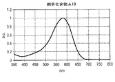
- FIG. 1 It is a cross-sectional schematic diagram which shows an example of embodiment in the organic photoelectric conversion element of this invention. It is a figure which shows the ultraviolet visible absorption spectrum of exemplary compound A2. It is a figure which shows the ultraviolet visible absorption spectrum of exemplary compound A19.
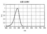
- 2 is a diagram showing an ultraviolet-visible absorption spectrum of Comparative Compound 1.
- FIG. 4 is a diagram showing an ultraviolet-visible absorption spectrum of Comparative Compound 2.
- the present invention relates to an organic photoelectric conversion element having an electron collection electrode, a hole collection electrode, and a photoelectric conversion unit disposed between the electron collection electrode and the hole collection electrode.
- the photoelectric conversion part has at least a first organic compound layer, and the first organic compound layer has a compound represented by the following general formula [1].
- FIG. 1 is a schematic cross-sectional view showing an example of an embodiment of the organic photoelectric conversion element of the present invention.
- the organic photoelectric conversion element 1 shown in FIG. 1 includes a hole collection electrode 13, an electron collection electrode 14, and a first organic layer disposed between the hole collection electrode 13 and the electron collection electrode 14. And a compound layer 10.
- a hole collecting electrode 13 constituting the organic photoelectric conversion element 1 shown in FIG. 1 is an electrode that collects holes that are one of the charges generated in the first organic compound layer 10.
- the electron collection electrode 14 is disposed closer to the pixel circuit (for example, the readout circuit 15) than the hole collection electrode 13.
- the hole collection electrode 13 may be disposed closer to the pixel circuit than the electron collection electrode 14.
- the first organic compound layer 10 has a compound that is excited by receiving light in the layer.
- the first organic compound layer 10 also has a role of transporting charges generated after the molecules of the compound are excited by light, that is, electrons and holes, to the electron collecting electrode 14 and the hole collecting electrode 13, respectively. Plays. Since the first organic compound layer 10 contains an organic compound that converts light into electric charges as will be described later, the first organic compound layer 10 is a layer constituting a photoelectric conversion layer or a photoelectric conversion unit.
- the photoelectric conversion part constituting the organic photoelectric conversion element is not limited to the first organic compound layer 10 alone.
- the first organic compound layer 10 is preferably a layer containing a p-type organic semiconductor or an n-type organic semiconductor.
- the first organic compound layer 10 is more preferably a bulk hetero layer (mixed layer) at least part of which includes a p-type organic semiconductor and an n-type organic semiconductor.
- the photoelectric conversion efficiency (sensitivity) of the device can be further improved. it can.
- the electron mobility in the first organic compound layer 10 and The hole mobility can be increased, and the light response speed of the organic photoelectric conversion element can be further increased.
- the first organic compound layer 10 is preferably composed of one layer, but may be composed of a plurality of layers. In the present invention, the first organic compound layer 10 preferably does not emit light.
- the term “non-light-emitting” as used herein refers to a layer having an emission quantum efficiency of 1% or less, preferably 0.5% or less, more preferably 0.1% or less in the visible light region (wavelength 400 nm to 730 nm). It means that.
- the emission quantum efficiency exceeds 1%, the sensing performance or imaging performance is improved when the organic photoelectric conversion device of the present invention is applied as a constituent member of a sensor or an imaging device. This is not preferable because it affects the operation. Details of the compounds that can be included in the first organic compound layer 10 will be described later.
- a second organic compound layer 11 is provided between the hole collection electrode 13 and the first organic compound layer 10.
- the second organic compound layer 11 may be composed of a single layer or a plurality of layers.
- the second organic compound layer 11 may be a bulk hetero layer (mixed layer) having a plurality of types of materials.
- the second organic compound layer 11 plays a role of transporting holes transferred from the first organic compound layer 10 to the hole collecting electrode 13. Further, the second organic compound layer 11 suppresses movement of electrons from the hole collection electrode 13 to the photoelectric conversion unit. That is, the second organic compound layer 11 functions as a hole transport layer or an electron blocking layer.
- the second organic compound layer 11 is preferably in contact with the hole collection electrode 13.
- a third organic compound layer 12 may be provided between the electron collection electrode 14 and the first organic compound layer 10.
- the third organic compound layer 12 is a layer provided between the first organic compound layer 10 and the electron collection electrode 14.
- the third organic compound layer 12 plays a role of transporting electrons moved from the first organic compound layer 10 to the electron collecting electrode 14.
- the third organic compound layer 12 is a layer (hole blocking layer) that suppresses the flow of holes from the electron collection electrode 14 to the first organic compound layer 10, and thus has a high ionization potential. It is preferable. As shown in FIG.
- the 3rd organic compound layer 12 when providing the 3rd organic compound layer 12, may be comprised by the single layer, and may be comprised by the some layer.
- the third organic compound layer 12 may be a bulk hetero layer (mixed layer) having a plurality of types of materials.
- the 3rd organic compound layer 12 is arrange
- the layers disposed between the electron collection electrode 14 and the hole collection electrode 13 are the above-described three types of layers (the first organic compound layer 10, the second organic compound layer 11, and the first layer). It is not limited to the three organic compound layers 12).
- An intervening layer can be further provided between the organic compound layer and the hole collecting electrode 13 or between the organic compound layer and the electron collecting electrode 14. This intervening layer is provided for the purpose of improving the injection efficiency of the charge when the generated charge is injected into the electrode, or preventing the charge from being injected into the organic compound layer when the charge is applied.
- the intervening layer may be an organic compound layer having an organic compound or an inorganic compound layer having an inorganic compound.
- the electron collection electrode 14 is connected to a readout circuit 15.
- the readout circuit 15 may be connected to the hole collection electrode 13.
- the readout circuit 15 reads out information based on the charges generated in the first organic compound layer 10 and plays a role of transmitting the information to, for example, a signal processing circuit (not shown) arranged in the subsequent stage.
- the readout circuit 15 includes, for example, a transistor that outputs a signal based on charges generated in the organic photoelectric conversion element 1.
- an inorganic protective layer 16 is disposed on the hole collecting electrode 13.
- the inorganic protective layer 16 includes an electron collection electrode 14, a third organic compound layer 12, a first organic compound layer 10, a second organic compound layer 11, and a hole collection electrode 13. It is a layer for protecting the member laminated
- the constituent material of the inorganic protective layer 16 include silicon oxide, silicon nitride, and aluminum oxide.
- the layer can be formed by a known film formation method.
- a color filter 17 is disposed on the inorganic protective layer 16.
- the color filter 17 include a color filter that transmits red light of visible light.
- the color filter 17 may be provided for one organic photoelectric conversion element or for a plurality of organic photoelectric conversion elements. Further, when the color filters 17 are arranged, for example, a Bayer arrangement may be formed with adjacent organic photoelectric conversion elements.
- an optical member such as a microlens 18 is disposed on the color filter 17.
- the microlens 18 plays a role of collecting incident light on the first organic compound layer 10 that is a photoelectric conversion unit.
- the number of microlenses 18 may be one for each organic photoelectric conversion element or one for a plurality of organic photoelectric conversion elements.
- one microlens 18 is preferably provided for each organic photoelectric conversion element.
- the voltage applied between both electrodes depends on the total film thickness of the organic compound layers (10, 11, 12), but is preferably 1 V or more and 15 V or less. More preferably, it is 2V or more and 10V or less.
- Ar 1 and Ar 2 are each independently an alkyl group having 1 to 8 carbon atoms, an aromatic hydrocarbon group having 6 to 18 carbon atoms, or a heteroaromatic group having 3 to 15 carbon atoms. Represents a cyclic group.
- alkyl group represented by Ar 1 and Ar 2 examples include methyl group, ethyl group, n-propyl group, iso-propyl group, n-butyl group, iso-butyl group, sec-butyl group, tert-butyl group, n -Pentyl group, n-hexyl group, cyclohexyl group, n-heptyl group, n-octyl group.
- a methyl group and a tert-butyl group are preferable.
- Examples of the aromatic hydrocarbon group represented by Ar 1 and Ar 2 include a phenyl group, a naphthyl group, a phenanthryl group, and a fluorenyl group. From the viewpoint of sublimability, a substituent having a relatively small molecular weight is preferable, and specifically, a phenyl group and a naphthyl group are preferable.
- Examples of the heteroaromatic ring group represented by Ar 1 and Ar 2 include a pyridyl group, a pyrazinyl group, a pyrimidinyl group, a quinolyl group, an isoquinolyl group, a thienyl group, a furanyl group, a benzothienyl group, a benzofuranyl group, and a triazinyl group.
- a substituent having a relatively small molecular weight and high stability is preferable, and specifically, a pyridyl group, a benzothienyl group, and a benzofuranyl group are preferable.
- Ar 1 and Ar 2 are each a halogen atom such as a fluorine atom, a chlorine atom, a bromine atom or an iodine atom, a cyano group, a methyl group, an ethyl group, an n-propyl group, an iso-propyl group, an n-butyl group, an iso An alkyl group having 1 to 6 carbon atoms such as a -butyl group, sec-butyl group, tert-butyl group, n-pentyl group, n-hexyl group, cyclohexyl group, phenyl group, tolyl group, xylyl group, mesityl group, and the like; You may further have a substituent selected from a cumenyl group.
- Ar 1 or Ar 2 further has an alkyl group having 1 to 6 carbon atoms
- the alkyl group is preferably a methyl group or a tert-butyl group.
- Ar 1 or Ar 2 further has a halogen atom, preferred as the halogen atom is a fluorine atom.
- Ar 1 and Ar 2 are an aromatic hydrocarbon group having 6 to 18 carbon atoms or a heteroaromatic group having 3 to 15 carbon atoms
- Ar 1 and Ar 2 are each a single bond, a methyl group May be bonded to each other via either a methylene group or an ethylene group which may have an alkyl group such as a ring structure, for example, the ring structure shown below.
- Ar 3 represents a condensed polycyclic aromatic hydrocarbon group constituted by condensation of 4 or 5 6-membered rings.
- substituents corresponding to the acene group specifically, tetracenediyl group and pentacenediyl group are excluded. In the present invention, the reason why the acene group is removed from the substituent represented by Ar 3 will be described later.
- the condensed polycyclic aromatic hydrocarbon group represented by Ar 3 is preferably a substituent selected from a pyrenediyl group, a benzopyrenediyl group, a triphenylenediyl group, a perylenediyl group, and a chrysenediyl group.
- a more preferable substituent as Ar 3 is a pyrenediyl group having a relatively small molecular weight.
- a perylenediyl group is more preferable as the substituent for Ar 3 .
- a more preferable substituent as Ar 3 is a pyrene-1,6-diyl group or a perylene-3,10-diyl group. This is because these substituents are substituents that are likely to cause transition of electrons among pyrenediyl groups and perylenediyl groups and that the absorption coefficient is improved.
- Ar 3 may further have a fluorine atom, a cyano group, a methyl group, or a tert-butyl group.
- Ar 2 and Ar 3 may be a single bond or an alkyl such as a methyl group. They may be bonded to each other via either a methylene group or an ethylene group, which may have a group, to form a ring structure, for example, the ring structure shown below.
- Q is a substituent selected from the substituent group represented by the following general formulas [2a] to [2e].
- substituent groups represented by the formulas [2a] to [2e] preferred are those of the formula [2a] which is a substituent having a relatively small molecular weight and high stability.
- R 1 to R 27 are each a substituent selected from a hydrogen atom, a fluorine atom, an alkyl group having 1 to 4 carbon atoms, and a cyano group.
- Examples of the alkyl group represented by R 1 to R 27 include a methyl group, an ethyl group, an n-propyl group, an iso-propyl group, an n-butyl group, an iso-butyl group, a sec-butyl group, and a tert-butyl group. Among these substituents, a methyl group or a tert-butyl group is preferable.
- the synthesis scheme of the formula [3] is a synthesis scheme in which the following reactions [3a] to [3c] are performed in this order.
- [3a] Reaction in which aryl dihalide and amine are cross-coupled on a one-to-one basis using Pd catalyst
- [3b] Reaction in which halide is formylated (ketone) using n-butyllithium
- [3c] Kune Fenergel condensation
- Ar 1 and Ar 2 in Formula [1], or Ar 2 and Ar 3 are bonded via a single bond, a methylene group (which may have an alkyl group) or an ethylene group to form a ring structure.
- a methylene group which may have an alkyl group
- an ethylene group to form a ring structure.
- the synthesis scheme of the formula [4] is a synthesis scheme in which the following reactions [4a] to [4f] are performed in this order.
- [4a] Reaction in which aryl halide and amine are cross-coupled on a one-to-one basis using Pd catalyst
- [4b] Formation of ring structure by Heck reaction
- [4c] Aryl halide and above [4b] using Pd catalyst A reaction for cross-coupling the amine having a ring structure formed in step [4d] Ar 3 (including a case where the substituent is included in the ring structure formed in [4b])
- Reaction [4e] Reaction of Formyl Halide Using n-Butyllithium
- [4f] Kunefener Gel Condensation
- the aryl halide used in the above [4a] is Ar If it is 1 -Br, Ar 1 and Ar 2 are a single bond, of having a ring structure formed by binding (via it may have an al
- FIG. 2 is a diagram showing an ultraviolet-visible absorption spectrum of exemplary compound A2 shown below.
- FIG. 3 is a figure which shows the ultraviolet visible absorption spectrum of exemplary compound A19 shown below.
- the UV-visible absorption spectrum is measured in a diluted toluene solution and at room temperature.
- model V-560 (trade name) manufactured by JASCO is used.
- the exemplary compound A2 had a maximum absorption wavelength of 546 nm and a half-value width in the visible light region of 198 nm (400 nm to 598 nm) as shown in FIG.
- the maximum absorption wavelength was 582 nm and the half width in the visible light region was 112 nm, as shown in FIG.
- Comparative compound 1 is compound 1-A disclosed in Patent Document 1
- Comparative compound 2 is compound 1-B disclosed in Patent Document 1.
- FIG. 4 is a diagram showing an ultraviolet-visible absorption spectrum of Comparative Compound 1.
- FIG. 5 is a view showing an ultraviolet-visible absorption spectrum of Comparative Compound 2.
- the measurement conditions of the ultraviolet-visible absorption spectrum are the same as those in the case of the exemplary compound A2 and the exemplary compound A19.
- the maximum absorption wavelength was 484 nm and the half-value width in the visible light region was 62 nm, as shown in FIG.
- the maximum absorption wavelength was 498 nm
- the half-value width in the visible light region was 76 nm, as shown in FIG.
- Comparative Compounds 1 and 2 have a narrow wavelength range of light absorbed by the compound itself, and in particular, there is almost no absorption in the red region (around 600 nm). Yes. For this reason, it is not suitable as a constituent material of an organic photoelectric conversion element.
- the compounds (Exemplary Compound A2, Exemplified Compound A19) corresponding to the compound of the general formula [1] have a wide absorption wavelength region of the compound itself, and the maximum absorption wavelength is shifted to the longer wavelength side.
- Comparative Compound 3 shown below in which the linking group contained in the compound is an anthracene-2,6-diyl group (condensed polycyclic aromatic hydrocarbon group). Comparative compound 3 is compound 1-C disclosed in Patent Document 1.
- Comparative Compound 3 was confirmed to be decomposed by oxidation during the synthesis, and could not be synthesized. This is considered because the comparative compound 3 has a reaction active site.
- acene a compound having a structure in which a plurality of benzene rings are linearly condensed.
- the structure becomes unstable as the number of condensed benzene rings increases (at least 3 or more).
- anthracene which is a typical compound of acene shown below, receives an electron donation from the benzene rings at both ends, so that the electron density of the central benzene ring is high. For this reason, anthracene is susceptible to an oxidation reaction in the central benzene ring. That is, anthracene has sites (active sites) unstable to oxidation at the 9th and 10th positions in the center.
- Comparative Compound 3 has an anthracene skeleton, which is an acene, as a partial structure. Further, in this anthracene skeleton, the substitution positions (9th and 10th positions) indicated by * in Table 1 are reactive active sites. For this reason, since the comparative compound 3 is a compound unstable to oxidation, it is not a suitable material as a constituent material of the organic photoelectric conversion element. On the other hand, the compounds corresponding to the compound represented by the general formula [1] (Exemplary Compound A2, Exemplified Compound A19) do not have a partial skeleton having a reaction active site, and thus are stable compounds against oxidation. is there.
- the compound of the general formula [1] is a compound having the properties (i) and (ii) above, it can perform photoelectric conversion in the entire visible light region as compared with the comparative compounds 1 to 3.
- the organic photoelectric conversion device having the compound of the general formula [1] has high stability of the device itself.
- a spin coat method is used as a method of forming the layer (1st organic compound layer 10) containing the compound of General formula [1]
- a spin coat method is used as a method of forming the layer (1st organic compound layer 10) containing the compound of General formula [1]
- vacuum deposition vacuum deposition method
- a compound having a lower molecular weight so that sublimation purification and film formation can be performed without excessive heating. Also, it is preferable to select a partial structure constituting the compound that does not have a reactive active substitution position, because the stability of the compound itself at a high temperature increases.
- Ar 1 and Ar 2 in the formula [1] when at least one of Ar 1 and Ar 2 in the formula [1] is an aromatic hydrocarbon group, a phenyl group and a naphthyl group are preferable because they have a relatively small molecular weight.
- Ar 1 and Ar 2 when at least one of Ar 1 and Ar 2 is a heteroaromatic ring group, a pyridyl group, a benzothienyl group, and a benzofuranyl group are preferable because they are relatively low molecular weight and highly stable substituents.
- the substituents of the formulas [2a] to [2c] are preferable because they are relatively low molecular weight and highly stable substituents.
- the organic photoelectric conversion element of the present invention whether or not the compound of the general formula [1] is present in the constituent members of the organic photoelectric conversion element such as the first organic compound layer 10 is included in the organic photoelectric conversion element.
- the layer can be verified by analyzing with TOF-SIMS or the like. Further, instead of the analysis by TOF-SIMS or the like, a method of extracting the constituent material of the organic photoelectric conversion element and analyzing it by IR, UV, NMR or the like may be employed.
- compounds having numbers beginning with A that is, compounds corresponding to Group A, have 6 carbon atoms in which Ar 1 and Ar 2 in formula [1] may have a substituent.
- the chemical stability of the compound itself is increased. Therefore, the compound corresponding to Group A is a compound having excellent thermal stability and sublimation properties.
- Exemplified Compounds A1 to A12 are such that Ar 3 in the formula [1] is a pyrenediyl group and Q in the formula [1] is any one of the general formulas [2a] to [2c] Therefore, the compound is particularly excellent in thermal stability and sublimation.
- the exemplified compounds A13 to A24 have Ar 3 in the formula [1] being a perylene diyl group and the substituent Q is any one of the general formulas [2a] to [2c], the longest absorption wavelength is particularly long. It is a compound excellent in wavelength conversion and sublimation.
- the exemplary compounds A3, A4, A15 and A16 have a methylene group or an ethylene group in which Ar 1 and Ar 2 , or Ar 2 and Ar 3 may have a single bond or an alkyl group (for example, a methyl group).
- a ring structure is formed by bonding via each other. Since the melting point of the compound itself is increased by the formation of this ring structure, the compound is excellent in thermal stability.
- a compound having a number beginning with B that is, a compound corresponding to group B is the number of carbon atoms in which either Ar 1 or Ar 2 in formula [1] may have a substituent. 3 to 15 heteroaromatic ring groups.
- the heteroaromatic ring has a nitrogen atom
- the electron withdrawing property of the nitrogen atom increases the oxidation potential of the compound itself (in other words, the oxidation potential becomes deeper), so that it is stable against oxidation.
- the heteroaromatic ring has a sulfur atom or an oxygen atom
- the sulfur atom or oxygen atom has many unshared electron pairs, so that the interaction between molecules is increased and the compound has an excellent carrier transport ability. That is, the compounds corresponding to Group B are particularly excellent compounds in terms of stability due to electronic effects and carrier transportability.
- the exemplary compounds B1 to B12 are particularly preferable because Ar 3 in the formula [1] is a pyrenediyl group and Q in the formula [1] is any one of the general formulas [2a] to [2c]. It is a compound with excellent thermal stability and sublimation properties.
- Exemplified compounds B13 to B24 are particularly maximal because Ar 3 in the formula [1] is a perylene diyl group and Q in the formula [1] is any one of the general formulas [2a] to [2c]. It is a compound that has a long absorption wavelength and excellent sublimation properties.
- the first organic compound layer 10 may be a layer made of only the compound of the general formula [1]. This is because the compound represented by the general formula [1] has a function of generating excitons by absorbing visible light and a function of generating and transporting charges, that is, holes and electrons, from the excitons. It is. In particular, the function of generating excitons by absorbing visible light is excellent.
- the first organic compound layer 10 may include other materials than the compound of the general formula [1].
- Other materials include a light-absorbing material that absorbs visible light and generates excitons, and a function that generates and transports charges, that is, holes and electrons, from excitons of the light-absorbing material.
- a photoelectric conversion induction material is mentioned.
- the first organic compound layer 10 includes a material (light absorption material, photoelectric conversion inducing material) other than the compound of the general formula [1]
- the light absorption material included in the first organic compound layer 10 may be one kind or two or more kinds.
- a photoelectric conversion part is a 1st organic compound which has a compound of General formula [1]
- a layered body in which the layer 10 and a layer having another material are stacked may be used.
- the photoelectric conversion part is comprised with the laminated body which laminates
- Photoelectric conversion-inducing materials other than the compound of general formula [1] include n-type organic semiconductors, specifically fullerene derivatives, naphthalene compounds such as NTCDI, perylene compounds such as PTCDI, phthalocyanine compounds such as SubPc, DCV3T, and the like. Examples include thiophene compounds.
- fullerene derivatives are preferable. Fullerene derivatives are particularly excellent in the function of generating and transporting charges (holes and electrons) from excitons among the n-type organic semiconductors described above, and also have the function of generating excitons by absorbing visible light. Because it is a material to prepare.
- One type of these photoelectric conversion inducing materials may be used, or two or more types may be used.
- Fullerene which is a skeleton that the fullerene derivatives have in common, is a generic name for closed-shell hollow clusters composed of only a large number of carbon atoms. Specific examples of the fullerene include C60 and higher-order fullerenes C70, C74, C76, and C78.
- a fullerene derivative is a compound in which a substituent such as an alkyl group, an aryl group, or a heterocyclic group is introduced into fullerene.
- fullerenes and fullerene derivatives may be collectively referred to as “fullerenes”.
- One of these compounds may be selected and used, or a plurality of types may be selected and used.
- Fullerenes contained in the first organic compound layer 10 can be used as an n-type organic semiconductor. Further, since the molecules of fullerene cause stacking between the fluoranthene skeletons, each molecule can be connected (oriented) in a certain direction in the first organic compound layer 10. Thereby, since an electron path is formed, the electron transport property is improved, and the high-speed response of the organic photoelectric conversion element is improved.
- the content of fullerenes contained in the first organic compound layer 10 is preferably 20% by volume or more and 80% by volume or less with respect to the entire first organic compound layer 10.
- fullerenes fullerene, fullerene derivative
- fullerene C60 fullerene C70, fullerene C76, fullerene C78, fullerene C80, fullerene C82, fullerene C84, fullerene C90, fullerene C96
- fullerene C240 fullerene 540, mixed fullerene, fullerene nanotubes, and fullerene derivatives shown below.
- the organic photoelectric conversion element of the present invention may have a substrate.
- the substrate include a silicon substrate, a glass substrate, and a flexible substrate.
- the constituent material of the hole collection electrode 13 is not particularly limited as long as it is a material having high conductivity and transparency.
- conductive metal oxides such as tin oxide (ATO, FTO) doped with antimony or fluorine, tin oxide, zinc oxide, indium oxide, indium tin oxide (ITO), zinc indium oxide, gold,
- Metal materials such as silver, chromium, nickel, titanium, tungsten and aluminum, and conductive compounds such as oxides and nitrides of these metal materials (for example, titanium nitride (TiN)), and these metals and conductive metal oxidation Examples thereof include a mixture or laminate with a material, an inorganic conductive material such as copper iodide and copper sulfide, an organic conductive material such as polyaniline, polythiophene and polypyrrole, and a laminate of these with ITO or titanium nitride.
- the constituent material of the hole collecting electrode 13 is particularly preferably a
- Electron Collection Electrode As a constituent material of the electron collection electrode 14, specifically, ITO, indium zinc oxide, SnO 2 , ATO (antimony-doped tin oxide), ZnO, AZO (Al-doped zinc oxide) , GZO (gallium-doped zinc oxide), TiO 2 , FTO (fluorine-doped tin oxide), and the like.
- the formation method of the two types of electrodes (13, 14) described above can be appropriately selected in consideration of suitability with the electrode material used for each. Specifically, it can be formed by a wet method such as a printing method or a coating method, a physical method such as a vacuum deposition method, a sputtering method, or an ion plating method, or a chemical method such as CVD or plasma CVD method.
- An electrode can be formed.
- the surface of the formed electrode (ITO electrode) may be subjected to UV-ozone treatment, plasma treatment, or the like.
- various film forming methods including a reactive sputtering method can be used.
- the formed electrode (TiN electrode) may be subjected to annealing treatment, UV-ozone treatment, plasma treatment, or the like.
- examples of the constituent material of the second organic compound layer 11 include organic compounds used as a hole transport material or a hole injection material. .
- the constituent material of the third organic compound layer 12 is a material having a high ionization potential, specifically, an electron transport material or an electron injection.
- the organic compound used as a material is mentioned. Since the first compound having a fullerene skeleton which is one of the constituent materials of the first organic compound layer 10 is a material having excellent electron transport properties as described above, the third organic compound layer It can be used as 12 constituent materials.
- the organic photoelectric conversion device of the present invention can be an organic photoelectric conversion device corresponding to light of different wavelengths by appropriately setting the constituent material of the first organic compound layer.
- the “wavelength” is the wavelength of light received by a predetermined organic photoelectric conversion element.
- FIG. An organic photoelectric conversion device is obtained that does not require the color filter shown.
- the plurality of types of organic photoelectric conversion elements included in the organic photoelectric conversion device at least one type of organic photoelectric conversion element is the organic photoelectric conversion element according to the present invention.
- the organic photoelectric conversion element according to the present invention can be used as a constituent member of an optical area sensor by being two-dimensionally arranged in the in-plane direction.
- the optical area sensor has a plurality of organic photoelectric conversion elements, and a plurality of organic photoelectric conversion elements are arranged in the front direction and the column direction, respectively.
- the organic photoelectric conversion element according to the present invention can be used as a constituent member of an imaging element.
- the imaging element has a plurality of organic photoelectric conversion elements each serving as a light receiving pixel, and a transistor connected to each organic photoelectric conversion element.
- a transistor here is a transistor which reads the electric charge generated from the organic photoelectric conversion element.
- Information based on the electric charge read by the transistor is transmitted to a sensor unit connected to the image sensor. Examples of the sensor unit include a CMOS sensor and a CCD sensor. An image can be obtained by collecting the information acquired by each light receiving pixel in the sensor unit.
- the image sensor may have, for example, an optical filter such as a color filter so as to correspond to each light receiving pixel.
- an optical filter such as a color filter so as to correspond to each light receiving pixel.
- the organic photoelectric conversion element supports light of a specific wavelength, it is preferable to have a color filter that transmits light in a wavelength region that can be handled by the organic photoelectric conversion element.
- One color filter may be provided for each light receiving pixel, or one color filter may be provided for a plurality of light receiving pixels.
- the optical filter included in the image pickup device is not limited to a color filter. Besides, a low-pass filter that transmits a wavelength equal to or greater than the wavelength of infrared light, a UV cut filter that transmits a wavelength equal to or smaller than the wavelength of ultraviolet light, and a long-pass filter Can be used.
- the imaging device may have an optical member such as a microlens so as to correspond to each light receiving pixel, for example.
- the microlens included in the image sensor is a lens that condenses light from the outside onto a photoelectric conversion unit included in the organic photoelectric conversion element included in the image sensor.
- One microlens may be provided for each light receiving pixel, or one microlens may be provided for a plurality of light receiving pixels. In the case where a plurality of light receiving pixels are provided, it is preferable that one microlens is provided for a plurality (two or more predetermined numbers) of light receiving pixels.
- the organic photoelectric conversion element according to the present invention can be used in an imaging apparatus.
- the imaging apparatus includes an imaging optical system having a plurality of lenses, and an imaging element that receives light that has passed through the imaging optical system.
- the imaging device may be an imaging device having a joint portion that can be joined to the imaging optical system and an imaging element. More specifically, the imaging device here refers to a digital camera or a digital still camera.
- the imaging device may further include a receiving unit that receives an external signal. The signal received by the receiving unit is a signal that controls at least one of the imaging range of the imaging apparatus, the start of imaging, and the end of imaging.
- the imaging device may further include a transmission unit that transmits an image acquired by imaging to the outside. As described above, the imaging device can be used as a network camera by including the reception unit and the transmission unit.
- the obtained exemplary compound A2 was identified by the following method.
- MALDI-TOF-MS Microx-Assisted Ionization-Time-of-Flight Mass Spectrometry
- Autoflex LRF (trade name) manufactured by Bruker)
- m / z 637.51
- C 46 H 39 NO 2 637.81
- ⁇ max the maximum absorption wavelength
- Synthesis Example 1 (1) cross-coupling reaction with arylamine
- the stability of the compound was decreased, and a decrease in purity was confirmed during column purification.
- Synthesis Example 1 (2) formylation reaction using n-butyllithium
- Comparative Compound 3 could not be obtained, and a device having Comparative Compound 3 was not produced.
- Example 1 Production of photoelectric conversion element On a substrate, a hole collection electrode, an electron blocking layer (second organic compound layer), a photoelectric conversion part (first organic compound layer), a hole blocking layer (first Three organic compound layers) and a photoelectric conversion element in which an electron collecting electrode is sequentially formed were produced by the method described below.
- an indium zinc oxide film was formed on a Si substrate, and then a hole collecting electrode was formed by performing a patterning process so as to have a desired shape. At this time, the thickness of the hole collecting electrode was set to 100 nm. Thus, the board
- an organic compound layer and an electrode layer shown in Table 2 below were continuously formed on the substrate with electrodes.
- the electrode area of the opposing electrode was set to 3 mm 2 .
- the following compound Y2 was used as the constituent material Z1 of an electron blocking layer.
- Example 1 Production of Photoelectric Conversion Element
- the constituent material Z1 of the second organic compound layer and the constituent materials Z2 and Z3 of the first organic compound layer are as follows. As shown in Table 2, an organic photoelectric conversion element was produced in the same manner as in Example 1 except that the materials were appropriately changed.
- the structures of the compound Y1 used in Examples 5, 10 and 12, and the compound Y3 used in Examples 3, 4 and 9 are shown below.
- Quantum yield External quantum efficiency was measured about the obtained organic photoelectric conversion element.
- the external quantum efficiency is a single color with an intensity of 50 ⁇ W / cm 2 at wavelengths of 450 nm, 500 nm, and 600 nm in a state where a voltage of 5 V is applied between the hole collecting electrode and the electron collecting electrode. It was calculated by measuring the density of the photocurrent that flows when the device was irradiated with light. The photocurrent density was determined by subtracting the dark current density during light shielding from the current density during light irradiation.
- the organic photoelectric conversion device according to the present invention has high external quantum efficiency in the blue region (wavelength around 450 nm), the green region (wavelength near 500 nm), and the red region (wavelength near 600 nm). It was found that photoelectric conversion can be performed efficiently over the entire region. On the other hand, in the organic photoelectric conversion element of the comparative example, it turned out that the photoelectric conversion efficiency in wavelength 600nm is small. This is because the half-value width of the absorption spectrum of the light-absorbing material included in the organic photoelectric conversion element according to the present invention is wide and the absorption is large even in the vicinity of a wavelength of 600 nm.
- organic photoelectric conversion element 10: first organic compound layer, 11: second organic compound layer (electron blocking layer), 12: third organic compound layer (hole blocking layer), 13: hole trapping Collector electrode, 14: electron collector electrode, 15: readout circuit, 16: inorganic protective layer, 17: color filter, 18: microlens
Landscapes
- Chemical & Material Sciences (AREA)
- Organic Chemistry (AREA)
- Engineering & Computer Science (AREA)
- Materials Engineering (AREA)
- Physics & Mathematics (AREA)
- Spectroscopy & Molecular Physics (AREA)
- Multimedia (AREA)
- Signal Processing (AREA)
- Electromagnetism (AREA)
- Nanotechnology (AREA)
- Light Receiving Elements (AREA)
- Photovoltaic Devices (AREA)
- Electroluminescent Light Sources (AREA)
- Solid State Image Pick-Up Elements (AREA)
- Transforming Light Signals Into Electric Signals (AREA)
Priority Applications (1)
| Application Number | Priority Date | Filing Date | Title |
|---|---|---|---|
| US16/114,686 US10873032B2 (en) | 2016-03-03 | 2018-08-28 | Organic photoelectric conversion element, two-dimensional sensor, image sensor, and imaging apparatus |
Applications Claiming Priority (2)
| Application Number | Priority Date | Filing Date | Title |
|---|---|---|---|
| JP2016040865A JP6645700B2 (ja) | 2016-03-03 | 2016-03-03 | 有機光電変換素子、二次元センサ、画像センサ及び撮像装置 |
| JP2016-040865 | 2016-03-03 |
Related Child Applications (1)
| Application Number | Title | Priority Date | Filing Date |
|---|---|---|---|
| US16/114,686 Continuation US10873032B2 (en) | 2016-03-03 | 2018-08-28 | Organic photoelectric conversion element, two-dimensional sensor, image sensor, and imaging apparatus |
Publications (1)
| Publication Number | Publication Date |
|---|---|
| WO2017149958A1 true WO2017149958A1 (ja) | 2017-09-08 |
Family
ID=59743721
Family Applications (1)
| Application Number | Title | Priority Date | Filing Date |
|---|---|---|---|
| PCT/JP2017/001226 Ceased WO2017149958A1 (ja) | 2016-03-03 | 2017-01-16 | 有機光電変換素子、二次元センサ、画像センサ及び撮像装置 |
Country Status (3)
| Country | Link |
|---|---|
| US (1) | US10873032B2 (https=) |
| JP (1) | JP6645700B2 (https=) |
| WO (1) | WO2017149958A1 (https=) |
Cited By (6)
| Publication number | Priority date | Publication date | Assignee | Title |
|---|---|---|---|---|
| US10861903B2 (en) | 2017-08-07 | 2020-12-08 | Canon Kabushiki Kaisha | Organic compound and photoelectric conversion element |
| US10868260B2 (en) | 2017-09-20 | 2020-12-15 | Canon Kabushiki Kaisha | Organic compound and photoelectric conversion element |
| US10873032B2 (en) | 2016-03-03 | 2020-12-22 | Canon Kabushiki Kaisha | Organic photoelectric conversion element, two-dimensional sensor, image sensor, and imaging apparatus |
| US11555028B2 (en) | 2017-10-25 | 2023-01-17 | Canon Kabushiki Kaisha | Organic compound and photoelectric conversion element |
| US11895910B2 (en) | 2017-08-23 | 2024-02-06 | Canon Kabushiki Kaisha | Organic compound and photoelectric conversion element |
| WO2025021855A1 (de) * | 2023-07-27 | 2025-01-30 | Merck Patent Gmbh | Materialien für organische lichtemittierende vorrichtungen und organische sensoren |
Families Citing this family (8)
| Publication number | Priority date | Publication date | Assignee | Title |
|---|---|---|---|---|
| JP2018014426A (ja) | 2016-07-21 | 2018-01-25 | キヤノン株式会社 | 有機化合物及びそれを有する有機光電変換素子 |
| JP7128584B2 (ja) * | 2017-10-26 | 2022-08-31 | 日本化薬株式会社 | 光電変換素子用材料及び光電変換素子 |
| EP3886182A4 (en) * | 2018-11-19 | 2022-03-30 | Panasonic Intellectual Property Management Co., Ltd. | OPTICAL SENSOR AND OPTICAL DETECTION SYSTEM |
| CN111454276B (zh) * | 2019-01-18 | 2022-01-11 | 北京夏禾科技有限公司 | 一种有机化合物及包含其的电致发光器件 |
| CN114195615A (zh) * | 2020-09-17 | 2022-03-18 | 香港科技大学 | 吸收光的主体材料、组合物、光学膜、其制备方法以及光电装置 |
| KR20240035755A (ko) | 2021-07-15 | 2024-03-18 | 닛테츠 케미컬 앤드 머티리얼 가부시키가이샤 | 촬상용의 광전 변환 소자용 재료 및 촬상용 광전 변환 소자 |
| US11867562B2 (en) * | 2022-01-25 | 2024-01-09 | Visera Technologies Company Limited | Optical devices |
| CN118108615A (zh) * | 2022-11-29 | 2024-05-31 | 中国科学院大连化学物理研究所 | 一种用于脂滴标记的高亮度荧光染料及其合成与应用 |
Citations (1)
| Publication number | Priority date | Publication date | Assignee | Title |
|---|---|---|---|---|
| JP2011213706A (ja) * | 2009-09-08 | 2011-10-27 | Fujifilm Corp | 光電変換材料、該材料を含む膜、光電変換素子及びその製造方法、光センサ、撮像素子、並びにそれらの使用方法 |
Family Cites Families (8)
| Publication number | Priority date | Publication date | Assignee | Title |
|---|---|---|---|---|
| US6833200B2 (en) | 1998-04-28 | 2004-12-21 | Canon Kabushiki Kaisha | Luminescent device with a triarylamine compound |
| US6583557B2 (en) | 2000-04-26 | 2003-06-24 | Canon Kabushiki Kaisha | Organic luminescent element |
| US8795855B2 (en) * | 2007-01-30 | 2014-08-05 | Global Oled Technology Llc | OLEDs having high efficiency and excellent lifetime |
| JP5108806B2 (ja) | 2008-03-07 | 2012-12-26 | 富士フイルム株式会社 | 光電変換素子及び撮像素子 |
| JP6077426B2 (ja) * | 2012-09-28 | 2017-02-08 | 富士フイルム株式会社 | 光電変換素子およびその使用方法、光センサ、撮像素子 |
| JP6645700B2 (ja) | 2016-03-03 | 2020-02-14 | キヤノン株式会社 | 有機光電変換素子、二次元センサ、画像センサ及び撮像装置 |
| JP2018014426A (ja) | 2016-07-21 | 2018-01-25 | キヤノン株式会社 | 有機化合物及びそれを有する有機光電変換素子 |
| EP3643763B1 (en) * | 2018-10-26 | 2023-04-26 | Canon Kabushiki Kaisha | Composition, organic light-emitting device, display device, photoelectric conversion apparatus, electronic apparatus, and moving object including the composition |
-
2016
- 2016-03-03 JP JP2016040865A patent/JP6645700B2/ja active Active
-
2017
- 2017-01-16 WO PCT/JP2017/001226 patent/WO2017149958A1/ja not_active Ceased
-
2018
- 2018-08-28 US US16/114,686 patent/US10873032B2/en active Active
Patent Citations (1)
| Publication number | Priority date | Publication date | Assignee | Title |
|---|---|---|---|---|
| JP2011213706A (ja) * | 2009-09-08 | 2011-10-27 | Fujifilm Corp | 光電変換材料、該材料を含む膜、光電変換素子及びその製造方法、光センサ、撮像素子、並びにそれらの使用方法 |
Non-Patent Citations (1)
| Title |
|---|
| ZHU, LIJUN ET AL.: "N-Annulated perylene dyes with adjustable photophysical properties", TETRAHEDRON LETTERS, vol. 52, no. 48, 2011, pages 6411 - 6414, XP028331478 * |
Cited By (7)
| Publication number | Priority date | Publication date | Assignee | Title |
|---|---|---|---|---|
| US10873032B2 (en) | 2016-03-03 | 2020-12-22 | Canon Kabushiki Kaisha | Organic photoelectric conversion element, two-dimensional sensor, image sensor, and imaging apparatus |
| US10861903B2 (en) | 2017-08-07 | 2020-12-08 | Canon Kabushiki Kaisha | Organic compound and photoelectric conversion element |
| US11895910B2 (en) | 2017-08-23 | 2024-02-06 | Canon Kabushiki Kaisha | Organic compound and photoelectric conversion element |
| US10868260B2 (en) | 2017-09-20 | 2020-12-15 | Canon Kabushiki Kaisha | Organic compound and photoelectric conversion element |
| US11793074B2 (en) | 2017-09-20 | 2023-10-17 | Canon Kabushiki Kaisha | Organic compound and photoelectric conversion element |
| US11555028B2 (en) | 2017-10-25 | 2023-01-17 | Canon Kabushiki Kaisha | Organic compound and photoelectric conversion element |
| WO2025021855A1 (de) * | 2023-07-27 | 2025-01-30 | Merck Patent Gmbh | Materialien für organische lichtemittierende vorrichtungen und organische sensoren |
Also Published As
| Publication number | Publication date |
|---|---|
| US20190013469A1 (en) | 2019-01-10 |
| JP6645700B2 (ja) | 2020-02-14 |
| JP2017157731A (ja) | 2017-09-07 |
| US10873032B2 (en) | 2020-12-22 |
Similar Documents
| Publication | Publication Date | Title |
|---|---|---|
| JP6645700B2 (ja) | 有機光電変換素子、二次元センサ、画像センサ及び撮像装置 | |
| JP7379444B2 (ja) | 有機化合物及び有機光電変換素子 | |
| JP6833351B2 (ja) | 有機光電変換素子、光エリアセンサ、撮像素子および撮像装置 | |
| JP6029606B2 (ja) | 光電変換素子、撮像素子、光センサ、光電変換素子の使用方法 | |
| JP6610257B2 (ja) | 光電変換素子ならびにそれを用いたイメージセンサ、太陽電池、単色検知センサおよびフレキシブルセンサ | |
| US11557727B2 (en) | Organic photoelectric conversion element, image pickup element, and image pickup apparatus | |
| TWI683463B (zh) | 光電轉換元件及使用其的影像感測器 | |
| WO2017138363A1 (ja) | 有機光電変換素子、光エリアセンサ、撮像素子及び撮像装置 | |
| JP2019031452A (ja) | 有機化合物及び光電変換素子 | |
| JP7791700B2 (ja) | インドロカルバゾール環を有する化合物、受光素子用材料、有機薄膜、受光素子、及び撮像素子 | |
| JP2018020976A (ja) | 有機化合物及びこれを用いた光電変換素子、光エリアセンサ、光電変換装置、撮像素子、撮像装置 | |
| JP7016662B2 (ja) | 有機化合物、それを用いた光電変換素子および撮像装置 | |
| JP2022013894A (ja) | 化合物及びそれを含む光電素子、赤外線吸収材、赤外線吸収/遮断フィルム、並びにセンサー及び電子装置 | |
| JP2024117715A (ja) | 光電変換素子、光電変換素子用材料、及び化合物 | |
| JP2017174921A (ja) | 有機光電変換素子、二次元センサ、画像センサ及び撮像装置 | |
| WO2022159769A1 (en) | Heteroaromatic photoactive compounds for transparent photovoltaic devices | |
| JP2017137264A (ja) | 有機化合物、赤外光吸収材料及びその利用 | |
| KR102788138B1 (ko) | 광전 변환 소자, 촬상 소자, 광 센서, 화합물 | |
| TWI611594B (zh) | 光電轉換元件、攝影元件、光感測器 | |
| WO2025013627A1 (ja) | 光電変換材料ならびにそれを用いた光電変換素子、光センサおよび表示装置 |
Legal Events
| Date | Code | Title | Description |
|---|---|---|---|
| NENP | Non-entry into the national phase |
Ref country code: DE |
|
| 121 | Ep: the epo has been informed by wipo that ep was designated in this application |
Ref document number: 17759430 Country of ref document: EP Kind code of ref document: A1 |
|
| 122 | Ep: pct application non-entry in european phase |
Ref document number: 17759430 Country of ref document: EP Kind code of ref document: A1 |