WO2017145910A1 - プラスチック基材ndフィルタ及び眼鏡用プラスチック基材ndフィルタ - Google Patents
プラスチック基材ndフィルタ及び眼鏡用プラスチック基材ndフィルタ Download PDFInfo
- Publication number
- WO2017145910A1 WO2017145910A1 PCT/JP2017/005732 JP2017005732W WO2017145910A1 WO 2017145910 A1 WO2017145910 A1 WO 2017145910A1 JP 2017005732 W JP2017005732 W JP 2017005732W WO 2017145910 A1 WO2017145910 A1 WO 2017145910A1
- Authority
- WO
- WIPO (PCT)
- Prior art keywords
- layer
- film
- nio
- substrate
- base material
- Prior art date
Links
Images


Classifications
-
- G—PHYSICS
- G02—OPTICS
- G02B—OPTICAL ELEMENTS, SYSTEMS OR APPARATUS
- G02B5/00—Optical elements other than lenses
- G02B5/20—Filters
- G02B5/205—Neutral density filters
-
- B—PERFORMING OPERATIONS; TRANSPORTING
- B32—LAYERED PRODUCTS
- B32B—LAYERED PRODUCTS, i.e. PRODUCTS BUILT-UP OF STRATA OF FLAT OR NON-FLAT, e.g. CELLULAR OR HONEYCOMB, FORM
- B32B27/00—Layered products comprising a layer of synthetic resin
- B32B27/06—Layered products comprising a layer of synthetic resin as the main or only constituent of a layer, which is next to another layer of the same or of a different material
- B32B27/08—Layered products comprising a layer of synthetic resin as the main or only constituent of a layer, which is next to another layer of the same or of a different material of synthetic resin
-
- B—PERFORMING OPERATIONS; TRANSPORTING
- B32—LAYERED PRODUCTS
- B32B—LAYERED PRODUCTS, i.e. PRODUCTS BUILT-UP OF STRATA OF FLAT OR NON-FLAT, e.g. CELLULAR OR HONEYCOMB, FORM
- B32B27/00—Layered products comprising a layer of synthetic resin
- B32B27/28—Layered products comprising a layer of synthetic resin comprising synthetic resins not wholly covered by any one of the sub-groups B32B27/30 - B32B27/42
-
- B—PERFORMING OPERATIONS; TRANSPORTING
- B32—LAYERED PRODUCTS
- B32B—LAYERED PRODUCTS, i.e. PRODUCTS BUILT-UP OF STRATA OF FLAT OR NON-FLAT, e.g. CELLULAR OR HONEYCOMB, FORM
- B32B27/00—Layered products comprising a layer of synthetic resin
- B32B27/40—Layered products comprising a layer of synthetic resin comprising polyurethanes
-
- B—PERFORMING OPERATIONS; TRANSPORTING
- B32—LAYERED PRODUCTS
- B32B—LAYERED PRODUCTS, i.e. PRODUCTS BUILT-UP OF STRATA OF FLAT OR NON-FLAT, e.g. CELLULAR OR HONEYCOMB, FORM
- B32B7/00—Layered products characterised by the relation between layers; Layered products characterised by the relative orientation of features between layers, or by the relative values of a measurable parameter between layers, i.e. products comprising layers having different physical, chemical or physicochemical properties; Layered products characterised by the interconnection of layers
- B32B7/02—Physical, chemical or physicochemical properties
- B32B7/023—Optical properties
-
- B—PERFORMING OPERATIONS; TRANSPORTING
- B32—LAYERED PRODUCTS
- B32B—LAYERED PRODUCTS, i.e. PRODUCTS BUILT-UP OF STRATA OF FLAT OR NON-FLAT, e.g. CELLULAR OR HONEYCOMB, FORM
- B32B9/00—Layered products comprising a layer of a particular substance not covered by groups B32B11/00 - B32B29/00
-
- G—PHYSICS
- G02—OPTICS
- G02B—OPTICAL ELEMENTS, SYSTEMS OR APPARATUS
- G02B1/00—Optical elements characterised by the material of which they are made; Optical coatings for optical elements
- G02B1/10—Optical coatings produced by application to, or surface treatment of, optical elements
- G02B1/11—Anti-reflection coatings
- G02B1/113—Anti-reflection coatings using inorganic layer materials only
- G02B1/115—Multilayers
-
- G—PHYSICS
- G02—OPTICS
- G02B—OPTICAL ELEMENTS, SYSTEMS OR APPARATUS
- G02B1/00—Optical elements characterised by the material of which they are made; Optical coatings for optical elements
- G02B1/10—Optical coatings produced by application to, or surface treatment of, optical elements
- G02B1/14—Protective coatings, e.g. hard coatings
-
- G—PHYSICS
- G02—OPTICS
- G02B—OPTICAL ELEMENTS, SYSTEMS OR APPARATUS
- G02B5/00—Optical elements other than lenses
-
- G—PHYSICS
- G02—OPTICS
- G02C—SPECTACLES; SUNGLASSES OR GOGGLES INSOFAR AS THEY HAVE THE SAME FEATURES AS SPECTACLES; CONTACT LENSES
- G02C7/00—Optical parts
- G02C7/10—Filters, e.g. for facilitating adaptation of the eyes to the dark; Sunglasses
-
- G—PHYSICS
- G02—OPTICS
- G02C—SPECTACLES; SUNGLASSES OR GOGGLES INSOFAR AS THEY HAVE THE SAME FEATURES AS SPECTACLES; CONTACT LENSES
- G02C7/00—Optical parts
- G02C7/10—Filters, e.g. for facilitating adaptation of the eyes to the dark; Sunglasses
- G02C7/107—Interference colour filters
-
- B—PERFORMING OPERATIONS; TRANSPORTING
- B32—LAYERED PRODUCTS
- B32B—LAYERED PRODUCTS, i.e. PRODUCTS BUILT-UP OF STRATA OF FLAT OR NON-FLAT, e.g. CELLULAR OR HONEYCOMB, FORM
- B32B2255/00—Coating on the layer surface
- B32B2255/10—Coating on the layer surface on synthetic resin layer or on natural or synthetic rubber layer
-
- B—PERFORMING OPERATIONS; TRANSPORTING
- B32—LAYERED PRODUCTS
- B32B—LAYERED PRODUCTS, i.e. PRODUCTS BUILT-UP OF STRATA OF FLAT OR NON-FLAT, e.g. CELLULAR OR HONEYCOMB, FORM
- B32B2255/00—Coating on the layer surface
- B32B2255/20—Inorganic coating
-
- B—PERFORMING OPERATIONS; TRANSPORTING
- B32—LAYERED PRODUCTS
- B32B—LAYERED PRODUCTS, i.e. PRODUCTS BUILT-UP OF STRATA OF FLAT OR NON-FLAT, e.g. CELLULAR OR HONEYCOMB, FORM
- B32B2551/00—Optical elements
Definitions
- the present invention relates to an ND (Neutral Density) filter whose base material is made of plastic, and an ND filter for glasses using the ND filter.
- ND Neutral Density
- This ND filter is formed by laminating a plurality of light absorption films and a plurality of dielectric films on one surface or both surfaces of a transparent substrate, and the light absorption film is composed of single germanium or single silicon. And a mixture of nickel and its oxide (Ni + NiO x ).
- the thing made from a plastic is preferable from a viewpoint of lightness, the difficulty of a crack, and dyeing
- the substrate is made of plastic, it is necessary to consider that the plastic is easy to absorb water and that the absorbed water is easily released. That is, the moisture released from the substrate gradually acts on the light absorption film and the dielectric film on the substrate, and the adhesion of these films gradually decreases, which can be a factor of gradually degrading the weather resistance and the like.
- Patent Document 1 there is no particular description about moisture from a plastic substrate, and in Patent Document 1 (plastic substrate), there is room for further improvement in terms of lifetime such as weather resistance.
- the present invention has the object of providing an ND filter and an ND filter for spectacles that have a base material (substrate) made of plastic and excellent in durability.
- an invention according to claim 1 is an ND filter comprising: a base material made of plastic; and a light absorption film having a plurality of layers disposed on at least one surface of the base material.
- the first layer of the layer from the substrate side of the light absorption layer is the Al 2 O 3 layer consisting of SiO 2 layer or Al 2 O 3 of SiO 2
- the light-absorbing film, NiO x (x is 0 or more and 1 or less) includes from consisting NiO x layer and CoO x '(x' is 0 to 1.5) comprising CoO x 'at least one of one or more of the layers from , At least one of at least one of the NiO x layer and the CoO x ′ layer is adjacent to the substrate side adjacent layer that is the layer adjacent on the substrate side, and adjacent to the opposite side.
- the invention according to claim 2 is the above invention, wherein at least one of the NiO x layer and the CoO x ′ layer has a physical film thickness of 6 nanometers or less. It is a feature.
- the invention according to claim 3 is characterized in that, in the above invention, the substrate side adjacent layer or the opposite side adjacent layer is a silica compound layer made of a silica compound.
- the invention according to claim 4 is characterized in that, in the above invention, the SiO 2 layer or the Al 2 O 3 layer has a density to the extent that it is formed by vapor deposition without ion assist.
- the invention according to claim 5 is characterized in that, in the above-mentioned invention, the light absorption film is formed by alternately arranging low refractive index layers and high refractive index layers.
- the invention according to claim 6 is characterized in that, in the above invention, the base material has a front surface and a back surface, and the light absorption film is disposed on the back surface.
- the invention according to claim 7 is the above invention, wherein an antireflection film is disposed on the surface.
- the invention according to claim 8 is a plastic substrate ND filter for eyeglasses, characterized by including the plastic substrate ND filter of the invention.
- an ND filter and an ND filter for spectacles that are made of plastic and have excellent durability.
- 4 is a graph showing spectral transmittance distributions in the visible range of Examples 1 to 4 according to the present invention.
- 7 is a graph showing spectral transmittance distributions in the visible range of Examples 5 to 8 according to the present invention. It is a graph by which the spectral transmittance distribution of a commercially available dyed spectacle lens is shown.
- 6 is a graph showing spectral reflectance distribution (single side) in the visible range on the concave surface (ND film formation surface) side of Examples 1 to 4.
- 10 is a graph showing spectral reflectance distribution (single side) in the visible range on the concave surface (ND film-forming surface) side of Examples 5 to 8.
- 10 is a graph showing spectral reflectance distributions (single side, common) in the visible range relating to the convex surface side of Examples 1 to 9.
- the ND filter according to the present invention has a light whose wavelength is at least in the visible range (for example, 400 nm to 800 nm, 400 nm to 760 nm, 400 nm to 700 nm, 410 nm to 760 nm, or 420 nm to 760 nm). It is a filter that uniformly absorbs (visible light).
- the substrate of the ND filter is made of transparent (including translucent as appropriate) plastic.
- the material of the substrate include polyurethane resin, thiourethane resin, episulfide resin, polycarbonate resin, acrylic resin, polyether sulfone resin, poly-4-methylpentene-1 resin, and diethylene glycol bisallyl carbonate resin.
- the base material may be a convex lens, a concave lens, a flat lens, or any power and progression.
- the ND filter of the present invention may be used for any application as long as the base material is made of plastic, and is preferably a part of a camera lens system (for protecting other lenses or for incorporating a camera body). And for projectors, binoculars, and telescopes, and more preferably for spectacles (use for spectacle lenses themselves or lenses that cover spectacle lenses).
- the optical multilayer film is formed on one side or both sides of the substrate.
- the optical multilayer film mainly has a function of uniformly absorbing visible light, and further has a function of appropriately preventing visible light reflection.
- the optical multilayer film for the purpose of absorbing visible light or a portion thereof is a light absorbing film, and when the light absorbing film is a single layer, it may be a light absorbing layer.
- the optical multilayer film or its part for the purpose of preventing reflection of visible light is an antireflection film.
- the antireflection film may include a light absorption film.
- the optical multilayer film may be composed only of the light absorption film, or may be one in which an antifouling film or a protective film is added to the surface side (air side) of the light absorption film,
- One or a plurality of intermediate layers including a hard coat film may be added to the base material side, or a single layer for other purposes such as improving conductivity in or outside the light absorption film.
- a plurality of layers or films may be added, or a combination thereof may be used.
- the hard coat film, the conductive layer, the antireflection film, and the like may not be included in the optical multilayer film, or may be separate optical multilayer films in combination with each other or in combination thereof.
- the hard coat film is formed from, for example, an organosiloxane compound, or formed from an organosilicon compound or an acrylic compound.
- a primer layer may be provided as a lower layer (layer on the substrate side) of the hard coat film.
- the primer layer is formed of at least one of polyurethane resin, acrylic resin, methacrylic resin, and organosilicon resin, for example.
- the antireflection film is formed of, for example, a plurality of types of dielectric materials including a low refractive index material and a high refractive index material.
- the low refractive index material at least one of the exemplary silicon oxide (especially SiO 2) or magnesium fluoride (in particular MgF 2), as the high refractive index material, zirconium oxide (in particular ZrO 2), titanium oxide (especially TiO 2 ), at least one of tantalum oxide (particularly Ta 2 O 5 ) and niobium oxide (particularly Nb 2 O 5 ).
- the antireflection film is preferably formed by alternately laminating a low refractive index material and a high refractive index material with one of them as the base material side.
- the light absorption film is formed to include one or more light absorption layers made of at least one of nickel (Ni) and cobalt (Co).
- Ni may be a simple substance, but is preferably an unsaturated metal oxide film (NiO x ; x is more than 0 and 1 or less).
- the value of x can be adjusted by, for example, Ni being used as a vapor deposition material and vapor deposition in a state where oxygen gas is supplied at a predetermined flow rate in a vapor deposition vacuum device.
- Co may be a simple substance, but is preferably an unsaturated metal oxide film (CoO x ′ ; x ′ exceeds 0 and is 1.5 or less).
- the light absorption film may be formed as a multilayer film having other layers. Examples of other layers in this case include an SiO 2 layer, a ZrO 2 layer, an aluminum oxide (particularly Al 2 O 3 ) layer, a silica compound layer, or a combination thereof.
- the silica compound is a compound of silicon or a mixture of the compound and another compound, preferably a mixture of silicon oxide and aluminum oxide, more preferably a mixture of SiO 2 and Al 2 O 3 . It is. At least one light-absorbing layer, i.e. NiO x layer (x is 0 or more and 1 or less) and CoO x 'layer (x' is 0 to 1.5) in at least one of, the base-side adjacent layer,
- the adjacent layers on the opposite side (air side) are layers made of different materials.
- the substrate side adjacent layer is an Al 2 O 3 layer
- the opposite side adjacent layer is a silica compound layer.
- the substrate side adjacent layer and the opposite side adjacent layer in at least one of the NiO x layers may be layers made of different materials.
- the substrate side adjacent layer and the opposite side adjacent layer in at least one of the NiO x layers may be layers made of different materials.
- both the NiO x layer and the CoO x ′ layer are provided one by one, in either one of the NiO x layer and the CoO x ′ layer, the substrate side adjacent layer and the opposite side adjacent layer are different from each other. It is sufficient to be a layer of.
- any one of the NiO x layer or the CoO x ′ layer is opposite to the substrate side adjacent layer.
- the adjacent layers may be layers made of different materials. If the base layer side adjacent layer or the opposite side adjacent layer is a silica compound layer, the silica compound layer has a density that does not allow moisture to pass as much as the ZrO 2 layer, and is not so dense that it completely seals moisture. It is preferable because the moisture permeability is just right.
- the first layer (initial layer) from the substrate side of the light absorption film is an SiO 2 layer or an Al 2 O 3 layer.
- the initial layer of the light absorption film has a density that can be formed by vapor deposition without ion assist. It is extremely difficult for those skilled in the art to directly measure the density of the deposited film including the initial layer. Also, it is easy to understand for those skilled in the art to specify the degree of density of the deposited film by the presence or absence of ion assist during deposition.
- the light absorption film may have a function as an antireflection film in addition to the light absorption function by alternately arranging the low refractive index layer and the high refractive index layer.
- the NiO x layer and the CoO x ′ layer may be treated as a high refractive index layer.
- the substrate preferably has a front and back surface such as for glasses.
- the front side of the ND filter substrate for glasses is the environment side, and the back side is the face side.
- the optical multilayer film preferably has an antireflection film disposed on the front side of the substrate and a light absorption film disposed on the back side.
- the anti-reflection coating is more durable than the light-absorbing film, the anti-reflection coating is relatively durable on the front side exposed to harsh environments, and the light-absorbing film is relatively protected on the back side. By disposing, it is possible to improve the overall durability while ensuring the light absorption (ND) and antireflection functions and realizing good characteristics.
- ND filter is preferably used for glasses.
- the ND filter itself may be a spectacle lens, or the ND filter may be prepared so as to cover another spectacle lens.
- General eyeglasses (sunglasses) have a visible light absorptance that varies greatly from wavelength to wavelength in the visible range, and look different from the naked eye in color, contrast, etc.
- the ND filter for eyeglasses of the present invention thus, visibility equal to that of the naked eye can be provided by uniform absorption of visible light in the visible range.
- Examples 1 to 8, Comparative Examples 1 to 7 several preferred examples of the present invention and comparative examples not belonging to the present invention will be described (Examples 1 to 8, Comparative Examples 1 to 7).
- an Example may turn into a comparative example or a comparative example may turn into an Example by the view of this invention.
- convex lenses for spectacles that are round balls having a diameter of 75 millimeters (mm) were produced.
- the frequency is S-4.00
- the convex side (front side) is aspherical
- the center thickness is 1.2 mm.
- the substrate both are formed of episulfide resin, the refractive index 1.76, Abbe number 30, a specific gravity of 1.49 g / cm 3 (grams per cubic centimeter).
- a hard coat film (HC film) was formed on both the front and back surfaces of the substrate. Each hard coat film was formed by applying the same hard coat liquid in the same manner.
- the hard coat solution was prepared as follows.
- the hard coat solution was uniformly spread on the surface of the substrate by a spin coat method, and then was hardened by heating in an environment of 120 ° C. for 1.5 hours to form a hard coat film.
- the physical film thickness of the hard coat film thus formed was 2.5 ⁇ m (micrometer).
- an antireflection film (AR film) and a water repellent layer were formed on the convex surface (surface) side of the substrate. That is, it is set on a jig (dome) to which a base material with a hard coat film is fixed, and is put into a vacuum apparatus from a door. Thereafter, the door is closed and the inside of the vacuum device is evacuated. In order to remove moisture from the substrate, the temperature in the vacuum apparatus is maintained at 60 ° C. When the degree of vacuum in the vacuum apparatus reaches 1.0E-03 (1.0 ⁇ 10 ⁇ 3 ) Pa (Pascal), the following film formation is started.
- the substrate surface is activated by irradiating the substrate surface with oxygen ions for 60 seconds.
- SiO 2 that is a low refractive material and ZrO 2 that is a high refractive material are alternately deposited for each predetermined time, and each layer has a desired film thickness, so that all five antireflection films are convex surfaces of the substrate.
- a film was formed on top.
- a water repellent was deposited on the convex side of the substrate with the antireflection film in a vacuum apparatus, and a water repellent layer was formed on the antireflection film (outermost layer).
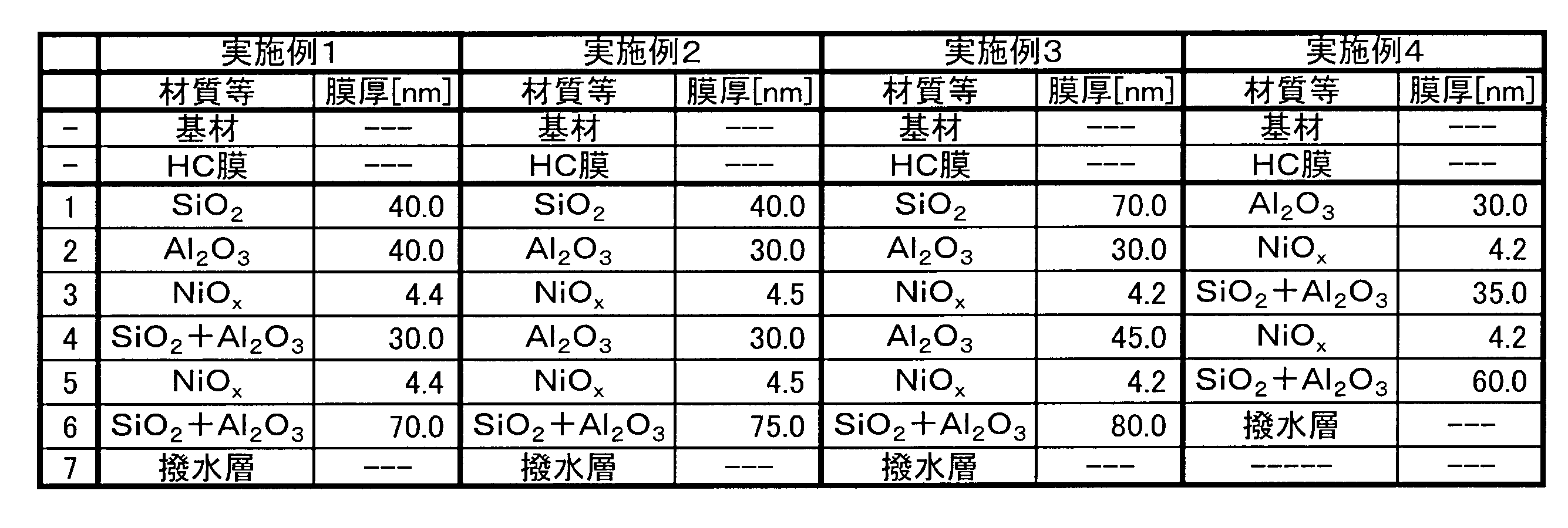
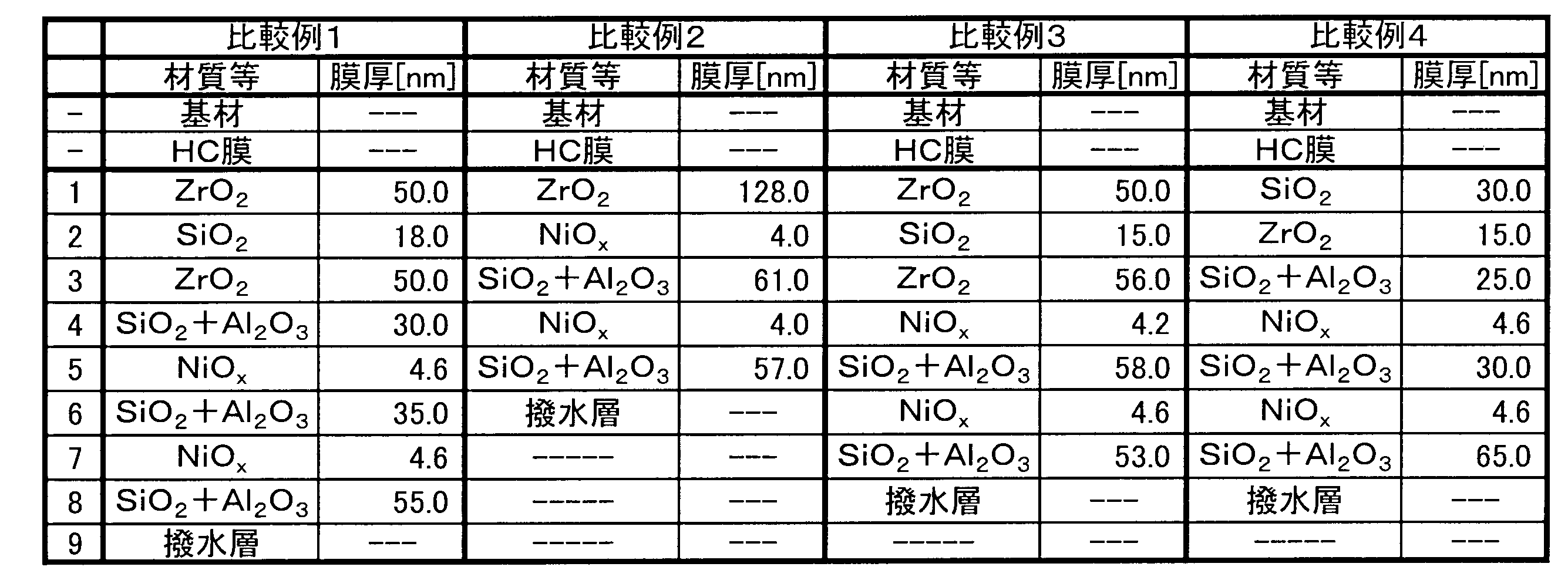
- Table 1 The structures of the optical multilayer films on the convex surface side in Examples 1 to 8 and Comparative Examples 1 to 7 are as shown in Table 1 below. Unless otherwise specified, the film thickness is a physical film thickness.
- the light absorption film and the water repellent layer were formed on the concave surface (back surface) side of the substrate. That is, the light absorption film is formed by adjusting the conditions at the time of starting the film formation, similarly to the formation of the antireflection film. In the film formation, after irradiating oxygen ions in the same manner, the next material was formed under the following conditions.
- the light-absorbing film deposition ions were not irradiated except for the first oxygen ion irradiation, and the light-absorbing film was deposited in a state without ion assist (in a state other than Ion Assist Deposition). As SiO 2, Canon Optron Co., Ltd.
- SiO 2 is used, it was deposited at a deposition rate 10.0 ⁇ / s (Angstrom per second).
- ZrO 2 “ZrO 2 ” manufactured by Canon Optron Co., Ltd. was used, and vapor deposition was performed at a deposition rate of 6.0 ⁇ / s.
- the weight of SiO 2 is higher than the weight of Al 2 O 3.
- the weight ratio of Al 2 O 3 to the weight ratio of SiO 2 is about several percent.
- the weight ratio between SiO 2 and Al 2 O 3 is not particularly limited, and the component of the silica compound is not limited to SiO 2 and Al 2 O 3 .
- NiO x and Co for CoO x ′ those manufactured by Kojundo Chemical Laboratory Co., Ltd. were used, and each was deposited at a deposition rate of 3.0 ⁇ / s.
- the oxygen gas is supplied at a flow rate 10sccm (standard cubic centimeter per minute) , NiO x layer and CoO x 'layer is formed.
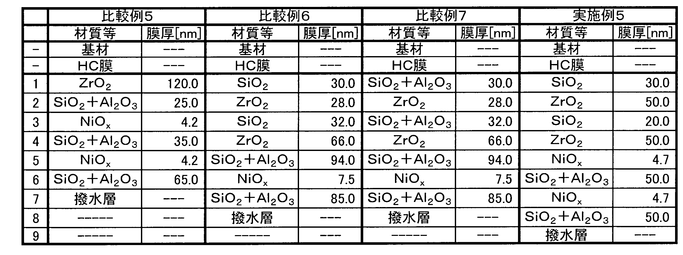
- a water repellent layer was formed on the light absorbing film (air side) in the same manner as that on the antireflection film. Examples 1 to 8 and Comparative Examples 1 to 7 differ from each other only in the configuration of the light absorption film. Each configuration is as described in Tables 2 to 5 below.
- Table 6 shows the result of the test regarding the presence / absence of ion assist and the density of the vapor deposition film (water vapor permeability closely related thereto) concerning the SiO 2 film and the Al 2 O 3 film.
- the "No.” column in Table 6 describes the order from the one having the highest water vapor permeability.
- This test uses a PET (polyethylene terephthalate) film as a base material, and changes the presence or absence of ion assist in the case of only the base material, and the SiO 2 film, Al 2 O 3 film, and SiO 2 + Al 2 O 3 mixed film on the base material
- the water vapor permeability (gram per cubic meter per day, g / m 2 ⁇ day) in the case of vapor deposition was investigated. In the case of only the base material, the water vapor permeability is 7.29.
- the SiO 2 film, the Al 2 O 3 film, the SiO 2 + Al 2 O 3 mixed film has a film thickness of 90.3 without ion assist.
- the water vapor permeability is 6.75, 6.28, 6.12, which is slightly lower than that of the base material alone.
- SiO 2 film, Al 2 O 3 film, the SiO 2 + Al 2 O 3 mixed film because hinder the permeation of water vapor.
- the SiO 2 film is ion-assisted (deposition with an ion gun acceleration voltage of 900 volts (V), an acceleration current of 900 milliamperes (mA), a bias current of 600 mA, and an introduced oxygen (O 2 ) gas of 50 sccm) with a film thickness of 69.1 nm. In this case, the water vapor permeability is further reduced to 3.77.
- the density of the SiO 2 film formed by ion-assisted deposition is larger than that without ion assist, and the SiO 2 film having such a high density further hinders the transmission of water vapor.
- the Al 2 O 3 film is deposited with an ion assist (acceleration voltage 1000 V, acceleration current 1000 mA, bias current 600 mA, introduced oxygen gas 50 sccm) and a film thickness of 79.0 nm, the water vapor permeability is 0.89. Decrease greatly. This is because the density of the Al 2 O 3 film formed by ion-assisted deposition is larger than the density without ion assist, and such a high-density Al 2 O 3 film further hinders the transmission of water vapor.
- the SiO 2 + Al 2 O 3 mixed film is deposited with a film thickness of 75.0 nm in the same ion assist state as the SiO 2 film, the water vapor permeability becomes as small as 1.61. This is because the density of the SiO 2 + Al 2 O 3 mixed film formed by ion-assisted deposition is larger than that without ion assist, and the higher density of the SiO 2 + Al 2 O 3 mixed film is made of water vapor. This is because transmission is further hindered.
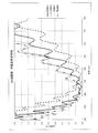
- FIG. 1 is a graph showing the spectral transmittance distribution in the visible range of Examples 1 to 4.
- the spectral transmittance distribution was measured with a spectrophotometer (U-4100 manufactured by Hitachi High-Technologies Corporation).
- the transmittance in the visible region is contained in a band-like region having 51 ⁇ 3%, and the visible light is uniformly absorbed at an absorption rate of about 50%.
- the ND filter for spectacles has a color that is recognized when worn without changing much from the naked eye view. The absorption rate when absorbing uniformly can be changed variously.
- FIG. 2 is a graph showing the spectral transmittance distribution in the visible range of Examples 5 to 8.
- Example 5 (NiO x layer) and Example 6 (CoO x ′ layer) exhibit the same spectral transmittance distribution as in Examples 1 to 4, and each of L, a, and b is the same as in Examples 1 to 4. Has a value.
- Example 5 the transmittance in the visible region is within the band-like region of 54 ⁇ 3%, and the visible light is uniformly absorbed at an absorption rate of about 46%, and the gray appearance is This is an ND filter for eyeglasses in which the color perceived at the time of wearing is not so different from that of naked eyes. Further, comparing Examples 5 and 6, it can be seen that the NiO x layer and the CoO x ′ layer have similar characteristics and can be used in the same manner. In Example 7, the number of light-absorbing layers (NiO x layers) is increased to 3 layers as compared with 2 layers in Examples 1 to 5, and thus the visible light absorption rate is higher than those in Examples 1 to 5. It has become.
- Example 7 the transmittance in the visible region is within a band-like region of 31 ⁇ 2%, and visible light is uniformly absorbed at an absorption rate of about 70%, and is recognized at the time of wearing even though it has a gray appearance.
- This is an ND filter for spectacles whose color is not so different from that of naked eyes.
- the seventh embodiment has the same values of a and b as the first to sixth embodiments, and the L value is smaller than the first to sixth embodiments.
- both the NiO x layer and the CoO x ′ layer are used as the light absorption layer.
- Example 8 the transmittance in the visible region is within a band-like region of 47 ⁇ 2%, and the visible light is uniformly absorbed at an absorption rate of about 53%, and is recognized at the time of wearing even though it has a gray appearance.
- This is an ND filter for spectacles whose color is not so different from that of naked eyes.
- Example 8 has the same values of a and b as in Examples 1 to 6, and the L value is slightly reduced compared to Examples 1 to 6.
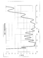
- FIG. 3 is a graph showing the spectral transmittance distribution of a dyed spectacle lens commercially available as gray sunglasses (50% concentration).
- This dyed eyeglass lens has a gray color as in Examples 1 to 8, and has a number of extreme values in the range of 45% to 94% in the spectral transmittance distribution in the visible region. The color of is greatly different from the color of the naked eye.
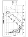
- FIG. 4 is a graph showing the spectral reflectance distribution (single side) in the visible range on the concave surface (ND film formation surface) side of Examples 1 to 4.
- the spectral reflectance distribution was measured by a reflectance measuring device (USPM-RU manufactured by Olympus Corporation).
- USPM-RU manufactured by Olympus Corporation
- the reflectance is generally 5% or less in the visible region, and the minimum value of the reflectance distribution in the green region (450 nm to 580 nm or less) that is greatly involved in the visibility (overall) Therefore, each light absorption film also has a function as an antireflection film.
- FIG. 5 is a graph similar to FIG. 4 on the concave surface (ND film formation surface) side of Examples 5 to 8.
- the reflectance is generally 5% or less in the visible region, and the reflectance distribution in the green region or its adjacent region (about 440 nm to 580 nm or less) that is greatly involved in visibility.
- each light absorption film also has a function as an antireflection film.
- FIG. 6 is a graph showing the spectral reflectance distribution (single side, common) in the visible range on the convex surface side of Examples 1 to 8 measured in the same manner.
- the reflectance is generally 5% or less in the visible region, and the reflectance is 2% or less in the region of 430 nm to 670 nm, which is the majority of the visible region.
- Tables 8 to 11 show the results of various tests relating to durability, that is, constant temperature and humidity test, concave weathering adhesion test, and salt water boiling test, for Examples 1 to 8 and Comparative Examples 1 to 7. Is shown.
- a constant temperature and humidity tester LHU-113 manufactured by ESPEC CORP.
- each ND filter was put in a test machine that was in an environment of 60 ° C. and 95%. After 1 day, 3 days, and 7 days from the start of charging, the ND filter was once taken out, and the presence or absence of appearance abnormalities such as swelling, discoloration, and cracks was observed.
- the ND filter is put into a sunshine weather meter (S80B, manufactured by Suga Test Instruments Co., Ltd.), and is taken out when the feeding time reaches 60 hours (hr), and the above-described cell formation, cellophane tape peeling and massing are performed five times. Number confirmation was done. Similarly, when the charging time became 120, 180, and 240 hours in total after the charging, the above-mentioned grid formation, stripping of the cellophane tape, and confirmation of the number of grids were performed.
- the salt water boiling test 45 g of sodium chloride and 1000 g of pure water were mixed to produce salt water, and the salt water was brought into a boiling state by a heater. And after each ND filter is immersed in boiling salt water and the total immersion time is 10, 20, 30, 40 minutes, the ND filter is taken out and the appearance is observed in the same manner as the constant temperature and humidity test. It was.
- Example 1 to 8 In all of Examples 1 to 8 and Comparative Examples 1 to 7, no abnormality in appearance such as peeling was observed in the salt water boiling test. Further, in Examples 1 to 8, in the constant temperature and humidity test, no abnormal appearance was observed even after 7 days (no change). However, in Example 5, no abnormality in appearance was observed after 3 days, but discoloration of the peripheral portion and generation of cracks were observed after 7 days. In Examples 1 to 8, no peeling was observed in all the squares in the weather resistance adhesion test (100/100).
- Comparative Example 1 in the weather resistance adhesion test, although partial peeling within one square was observed after completion of the total of five peelings in 120 hours and 180 hours (99.5 / 100), other peeling was observed. Good weather resistance was shown. However, in the constant temperature and humidity test, discoloration of the central part was observed after 1 day, and cracks were observed after 3 days. Discoloration is observed in the NiO x layer, and it is considered that the discoloration is due to the action of moisture. The crack is generated on the concave surface, and is considered to be generated according to the stress balance state of the light absorption film. In Comparative Example 1, the first layer from the substrate side (hereinafter the same) is not a SiO 2 layer or an Al 2 O 3 layer but a ZrO 2 layer.
- the ZrO 2 layer has a film density that is too small compared to the SiO 2 layer or Al 2 O 3 layer, allowing water vapor to pass through, and the moisture from the plastic substrate immediately reaches the second and subsequent layers, especially the NiO x layer. It is thought to affect and cause discoloration. From the viewpoint of improving the film density of the first layer, it is assumed that the density is increased by depositing the first layer of Examples 1 to 8 with ion assist. However, with ion assist, the density is too high so that water vapor hardly passes (see Table 6), and the moisture of the base material is accumulated by losing the escape field on the concave surface.
- the light-absorbing film passes through a weak point at a single point, and exhibits a point-like appearance abnormality.
- the first layer has a density related to a state without ion assist.
- the adjacent layer on the substrate side of the two NiO x layers and the adjacent layer on the opposite side are both SiO 2 + Al 2 O 3 mixed layers.
- the SiO 2 + Al 2 O 3 mixed layer has a relatively high density and hardly allows moisture to pass through compared to the SiO 2 layer and the Al 2 O 3 layer (having a high packing effect due to a dense structure).
- Example 1 the second layer of Al 2 O 3 which is the base layer side adjacent layer of the third layer of NiO x is mixed with the fourth layer of SiO 2 + Al 2 O 3 which is the opposite side adjacent layer. Since the material is different from the layer, stress can be released from the adjacent layer on the base material side.
- the base layer side adjacent layer (fourth layer) and the opposite side adjacent layer (sixth layer) of the fifth NiO x layer are both SiO 2 + Al 2 O 3 mixed layers, but the second layer Al 2 Stress can be relieved by the O 3 layer.
- the sixth layer SiO 2 + Al 2 O 3 mixed layer which is the adjacent layer on the opposite side of the fifth NiO x layer, is the fourth layer Al 2 O 3 which is the substrate side adjacent layer. Since the material is different from the layer, stress can be released from the adjacent layer on the opposite side. Further, CoO x 'layer and, NiO x layer and CoO x Example 8' of Example 6 is also in at least one of the layers, as with NiO x layers of Examples 1 to 5 and 7, at least one light-absorbing If the materials of the base layer side adjacent layer and the opposite side adjacent layer are different from each other in the layer, the stress is relieved and the generation of cracks is prevented. It should be noted that the packing effect and the stress difference in SiO 2 + Al 2 O 3 mixed layer, it is same tendency in other silica compounds.
- Comparative Example 2 in the weather resistance adhesion test, no peeling was observed at any time, and good weather resistance was shown. However, in the constant temperature and humidity test, an extremely thin spot (discoloration) is recognized in the peripheral part (end part) after 1 day, and after 7 days, the end spot becomes dark and linear discoloration occurs. The situation is confirmed.
- the first ZrO 2 layer in Comparative Example 2 is more permeable to moisture than the SiO 2 layer or the Al 2 O 3 layer, and the moisture released from the plastic substrate is two layers in the periphery. It is considered that the NiO x layer was reached and the NiO x layer was modified.
- the first layer of the light absorption film is a SiO 2 layer or an Al 2 O 3 layer
- the moisture does not pass as much as the ZrO 2 layer, and the NiO x layer is prevented from being modified by moisture. Is done.
- the first layer of the SiO 2 layer or the Al 2 O 3 layer is the density enough to be formed by vapor deposition without ion assist, likelihood of the point of color change can be further reduced More preferable.
- Comparative Example 3 in the weather resistance adhesion test, no peeling was observed at any time, and good weather resistance was shown. However, in the constant temperature and humidity test, linear discoloration occurred as a whole after 1 day, and an increase in discoloration in the center was further observed after 7 days. Configuration of the light absorbing film of Comparative Example 3, the SiO 2 layer and the ZrO 2 layer applied between the first layer and the second layer of Comparative Example 2 was small thickness of that amount first layer of ZrO 2 layer In other words, the first layer of Comparative Example 2 is divided into three layers, but the test results cannot be improved as compared with Comparative Example 2, and therefore even if the first layer is divided. If the first layer is a ZrO 2 layer, it is considered that the influence of moisture permeation on the NiO x layer cannot be prevented.
- Comparative Example 4 in the weather resistance adhesion test, a mass with peeling occurred from the initial stage, and only 10 squares remained without peeling when a total of 5 peelings were completed in 60 hours, and the subsequent test was stopped. . In the constant temperature and humidity test, cracks in the center were observed after 1 day. Thus, Comparative Example 4 is poor in weather resistance, temperature resistance, and moisture resistance. This is because, as in Comparative Example 1, Comparative Example 4 has a structure in which any NiO x layer is sandwiched between SiO 2 + Al 2 O 3 mixed layers and maintains a state in which the stress balance is lost. It is considered a thing.
- Comparative Example 4 no discoloration occurred, and it is considered that if the SiO 2 layer is the first layer, it is possible to prevent moisture from reaching the NiO x layer.
- Comparative Example 3 although the SiO 2 layer is disposed as the second layer, since the first layer is the ZrO 2 layer, it is not possible to prevent moisture from reaching the NiO x layer.
- Comparative Example 5 no abnormal appearance was observed even after 7 days in the constant temperature and humidity test. However, in the weather resistance adhesion test, many peelings were recognized in 60 hours.
- the first layer is a ZrO 2 layer that allows moisture to pass therethrough, and the third and fifth NiO x layers are sandwiched between SiO 2 + Al 2 O 3 mixed layers as in Comparative Example 1. It is thought that the weather resistance was affected.
- the NiO x layer becomes porous by that amount, and when the cross-sectional area of the pores in the porous NiO x layer exceeds a threshold value, moisture enters from the pores, NiO x layer is made to be altered.
- the thickness of the NiO x layer is 7.5 nm for absorption of visible light, and the porosity at the end portion appears relatively prominently, mainly due to moisture from the atmosphere side. It is considered that the NiO x layer is modified and discolored.
- the thickness of the NiO x layer is 4.2 nm or more and 4.7 nm or less, and the influence of the porous structure at the end is reduced.
- the NiO x layer is thin, the difference in stress with respect to the adjacent layers is reduced accordingly. Also in the CoO x ′ layers of Examples 6 and 8, the film thickness is similarly 4.5 nm or less, and the influence of the porosity at the end is alleviated. Examples 1-8, Comparative Examples 1-7 and from the results of the simulation, the thickness of the NiO x layer and CoO x 'layer is not more 6nm or less, relaxation effect of porosity and stress differences are exhibited good I understood that. In the case where the absorption amount of visible light becomes insufficient by making the NiO x layer or CoO x ′ layer thin, a plurality of layers (6 nm or less) may be provided (division of the light absorption layer).
- Comparative Example 7 similar to Comparative Example 6, crescent-like discoloration was observed after 1 day.
- the thickness of the NiO x layer (sixth layer) is relatively large, and the substrate side adjacent layer (fifth layer) and the opposite side adjacent layer (seventh layer) of the NiO x layer are both It is a SiO 2 + Al 2 O 3 mixed layer, and it is thought that the influence of the stress difference and the porous structure is exerted particularly on the end portion.
- the substrate side in at least one light absorption layer (at least one of the NiO x layer and the CoO x ′ layer, or a plurality of layers when there are a plurality of layers) If the material of the layer is made different between the adjacent layer and the adjacent layer on the opposite side, the substrate is made of plastic, and an ND filter having excellent durability can be provided.
Landscapes
- Physics & Mathematics (AREA)
- General Physics & Mathematics (AREA)
- Optics & Photonics (AREA)
- Health & Medical Sciences (AREA)
- Ophthalmology & Optometry (AREA)
- General Health & Medical Sciences (AREA)
- Chemical & Material Sciences (AREA)
- Inorganic Chemistry (AREA)
- Surface Treatment Of Optical Elements (AREA)
- Laminated Bodies (AREA)
- Eyeglasses (AREA)
- Optical Elements Other Than Lenses (AREA)
- Physical Vapour Deposition (AREA)
Abstract
【課題】基材がプラスチック製であり、耐久性に優れたNDフィルタ,眼鏡用NDフィルタを提供する。 【解決手段】NDフィルタにおいて、基材がプラスチックであり、基材の少なくとも一面には、複数の層を有する光吸収膜が配置される。光吸収膜の基材側から1層目の層(初期層)は、SiO2層又はAl2O3層とされている。又、光吸収膜は、NiOx(xは0以上1以下)からなるNiOx層を1つ以上含んでおり、少なくとも1つの前記NiOx層は、基材側で隣接する前記層である基材側隣接層と、その反対側で隣接する前記層であって前記基材側隣接層と材質の異なる反対側隣接層とで挟まれている。
Description
本発明は、基材がプラスチック製であるND(Neutral Density)フィルタ、及び当該NDフィルタを用いた眼鏡用NDフィルタに関する。
NDフィルタとして、下記特許文献1のものが知られている。
このNDフィルタは、透明な基板の一方の面あるいは両面に複数の光吸収膜と複数の誘電体膜を積層状に成膜させて構成されており、その光吸収膜は、単体ゲルマニウム又は単体シリコンと、ニッケル及びその酸化物の混合体(Ni+NiOx)を含んでいる。
このNDフィルタは、透明な基板の一方の面あるいは両面に複数の光吸収膜と複数の誘電体膜を積層状に成膜させて構成されており、その光吸収膜は、単体ゲルマニウム又は単体シリコンと、ニッケル及びその酸化物の混合体(Ni+NiOx)を含んでいる。
特許文献1のものにおいて、基板は強化ガラス製のものやプラスチック製のものが想定されるところ、軽さや割れ難さ、染色容易性の観点からはプラスチック製のものが好ましく、眼鏡用であれば尚更である。
基板がプラスチック製である場合、プラスチックは吸水し易く又吸水した水分を徐放し易いことに配慮する必要がある。即ち、基板から徐放された水分は、基板上の光吸収膜や誘電体膜に徐々に作用して、これらの膜の密着性が漸減し、耐候性等が徐々に劣化する要因となり得る。特許文献1では、プラスチック製の基板からの水分について特段の記載はなく、特許文献1のもの(プラスチック基板)では、耐候性等の寿命に関し、更なる向上の余地がある。
そこで、請求項1,8に記載の発明は、基材(基板)がプラスチック製であり、耐久性に優れたNDフィルタ,眼鏡用NDフィルタを提供することを目的とするものである。
基板がプラスチック製である場合、プラスチックは吸水し易く又吸水した水分を徐放し易いことに配慮する必要がある。即ち、基板から徐放された水分は、基板上の光吸収膜や誘電体膜に徐々に作用して、これらの膜の密着性が漸減し、耐候性等が徐々に劣化する要因となり得る。特許文献1では、プラスチック製の基板からの水分について特段の記載はなく、特許文献1のもの(プラスチック基板)では、耐候性等の寿命に関し、更なる向上の余地がある。
そこで、請求項1,8に記載の発明は、基材(基板)がプラスチック製であり、耐久性に優れたNDフィルタ,眼鏡用NDフィルタを提供することを目的とするものである。
上記目的を達成するために、請求項1に記載の発明は、NDフィルタであって、プラスチックからなる基材と、前記基材の少なくとも一面に配置された、複数の層を有する光吸収膜を備えており、前記光吸収膜における前記基材側から1層目の前記層は、SiO2からなるSiO2層又はAl2O3からなるAl2O3層であり、前記光吸収膜は、NiOx(xは0以上1以下)からなるNiOx層及びCoOx’(x’は0以上1.5以下)からなるCoOx’層のうちの少なくとも何れか一方を1つ以上含んでおり、前記NiOx層及び前記CoOx’層のうちの少なくとも何れか一方における少なくとも何れか1つは、基材側で隣接する前記層である基材側隣接層と、その反対側で隣接する前記層であって前記基材側隣接層と材質の異なる反対側隣接層とで挟まれていることを特徴とするものである。
請求項2に記載の発明は、上記発明にあって、前記NiOx層及びCoOx’層のうちの少なくとも一方は、何れも物理膜厚が6ナノメートル以下であるものとされていることを特徴とするものである。
請求項3に記載の発明は、上記発明において、前記基材側隣接層又は前記反対側隣接層は、シリカ化合物からなるシリカ化合物層であることを特徴とするものである。
請求項4に記載の発明は、上記発明において、前記SiO2層又は前記Al2O3層は、イオンアシストのない蒸着によって形成される程度の密度を有することを特徴とするものである。
請求項5に記載の発明は、上記発明において、前記光吸収膜は、低屈折率層と高屈折率層が交互に配置されたものであることを特徴とするものである。
請求項6に記載の発明は、上記発明において、前記基材には、表面と裏面が存在しており、前記光吸収膜は、前記裏面に配置されていることを特徴とするものである。
請求項7に記載の発明は、上記発明において、前記表面には、反射防止膜が配置されていることを特徴とするものである。
請求項8に記載の発明は、眼鏡用プラスチック基材NDフィルタであって、上記発明のプラスチック基材NDフィルタを含んでいることを特徴とするものである。
本発明によれば、基材がプラスチック製であり、耐久性に優れたNDフィルタ,眼鏡用NDフィルタを提供することが可能となる、という効果を奏する。
以下、本発明に係る実施の形態の例につき、適宜図面を用いて説明する。尚、本発明の形態は、以下のものに限定されない。
本発明に係るNDフィルタは、少なくとも波長が可視域(例えば400ナノメートル(nm)以上800nm以下、400nm以上760nm以下、400nm以上700nm以下、410nm以上760nm以下、又は420nm以上760nm以下)内である光(可視光)を均一に吸収するフィルタである。
NDフィルタの基材は、透明(半透明を適宜含む)なプラスチック製である。基材の材質の例としては、ポリウレタン樹脂、チオウレタン樹脂、エピスルフィド樹脂、ポリカーボネート樹脂、アクリル樹脂、ポリエーテルサルホン樹脂、ポリ4-メチルペンテン-1樹脂、ジエチレングリコールビスアリルカーボネート樹脂が挙げられる。
又、基材は、凸レンズであっても良いし、凹レンズであっても良いし、フラットレンズであっても良く、度数や累進もどのようなものであっても良い。
本発明のNDフィルタは、基材がプラスチック製のものであれば、どのような用途で用いられても良く、好適にはカメラレンズ系の一部(他のレンズの保護用やカメラ本体内蔵用を含む)に含ませるためのカメラ用、又同様にプロジェクタ用、双眼鏡用、望遠鏡用であり、更に好適には眼鏡用(眼鏡レンズ自体とする用途や眼鏡レンズに被さるレンズ用)である。
又、基材は、凸レンズであっても良いし、凹レンズであっても良いし、フラットレンズであっても良く、度数や累進もどのようなものであっても良い。
本発明のNDフィルタは、基材がプラスチック製のものであれば、どのような用途で用いられても良く、好適にはカメラレンズ系の一部(他のレンズの保護用やカメラ本体内蔵用を含む)に含ませるためのカメラ用、又同様にプロジェクタ用、双眼鏡用、望遠鏡用であり、更に好適には眼鏡用(眼鏡レンズ自体とする用途や眼鏡レンズに被さるレンズ用)である。
基材の片面あるいは両面には、光学多層膜が形成されている。
光学多層膜は、主に可視光を均一に吸収する機能を具備しており、更に適宜可視光の反射を防止する機能を具備する。可視光の吸収を目的とした光学多層膜あるいはその部分は光吸収膜であり、光吸収膜が1つの層である場合には光吸収層とすることもある。又、可視光の反射防止を目的とした光学多層膜あるいはその部分は、反射防止膜である。反射防止膜は、光吸収膜を含むことがある。基材の両面に光学多層膜が配置される場合、双方の光学多層膜が同一の構成とされても良いし、互いに異なる構成とされても良い。
光学多層膜は、光吸収膜のみから構成されても良いし、光吸収膜の表面側(空気側)に防汚膜や保護膜が付加されたものであっても良いし、光吸収膜の基材側にハードコート膜を始めとする中間層が単数又は複数付加されたものであっても良いし、光吸収膜内あるいは光吸収膜外に導電性向上等の他の目的のための単数又は複数の層や膜が付加されたものであっても良いし、これらの組合せであっても良い。尚、ハードコート膜や導電層、反射防止膜等は、光学多層膜に含まれないものとされたり、それぞれあるいはこれらの組合せで別個の光学多層膜であるものとされたりしても良い。
ハードコート膜は、例えば、オルガノシロキサン系化合物から形成され、あるいは有機ケイ素化合物、又はアクリル化合物から形成される。
ハードコート膜の下層(基材側の層)として、プライマー層が設けられても良い。プライマー層は、例えば、ポリウレタン系樹脂、アクリル系樹脂、メタクリル系樹脂、有機ケイ素系樹脂の少なくとも何れかから形成される。
ハードコート膜の下層(基材側の層)として、プライマー層が設けられても良い。プライマー層は、例えば、ポリウレタン系樹脂、アクリル系樹脂、メタクリル系樹脂、有機ケイ素系樹脂の少なくとも何れかから形成される。
反射防止膜は、例えば、低屈折率材料及び高屈折率材料を含む複数種類の誘電体材料から形成される。低屈折率材料としては、酸化ケイ素(特にSiO2)やフッ化マグネシウム(特にMgF2)の少なくとも一方が例示され、高屈折率材料としては、酸化ジルコニウム(特にZrO2)、酸化チタン(特にTiO2)、酸化タンタル(特にTa2O5)、酸化ニオブ(特にNb2O5)の少なくとも何れかが例示される。反射防止膜は、好ましくは、低屈折率材料と高屈折率材料が、何れか一方を基材側として交互に積層されることで形成される。
光吸収膜は、ニッケル(Ni)及びコバルト(Co)の少なくとも一方からなる光吸収層を1層あるいは2層以上含むように形成される。
Niは、単体でも良いが、好ましくは不飽和金属酸化膜(NiOx;xは0を超えて1以下)である。xの値は、例えばNiが蒸着材料とされ、蒸着用真空装置内に酸素ガスを所定流量で供給した状態で蒸着されることで調整可能であり、酸素ガスを流さなければx=0(単体)となる。
Coは、単体でも良いが、好ましくは不飽和金属酸化膜(CoOx’;x’は0を超えて1.5以下)である。xの値は、例えばCoが蒸着材料とされ、蒸着用真空装置内に酸素ガスを所定流量で供給した状態で蒸着されることで調整可能であり、酸素ガスを流さなければx’=0(単体)となる。
光吸収膜は、他の層を有する多層膜として形成されても良い。この場合の他の層として、例えば、SiO2層、ZrO2層、酸化アルミニウム(特にAl2O3)層、シリカ化合物層、あるいはこれらの組合せが例示される。ここで、シリカ化合物は、ケイ素の化合物あるいはその化合物と他の化合物の混合体であるが、好ましくは酸化ケイ素と酸化アルミニウムの混合体であり、より好ましくはSiO2とAl2O3の混合体である。
少なくとも1つの光吸収層、即ちNiOx層(xは0以上1以下)及びCoOx’層(x’は0以上1.5以下)の少なくとも何れか一方における、基材側の隣接層と、その反対側(空気側)の隣接層は、互いに異なる材質の層とされる。例えば、基材側隣接層がAl2O3層で、反対側隣接層がシリカ化合物層とされる。
NiOx層が複数設けられる場合、少なくとも何れか1つのNiOx層における、基材側隣接層と反対側隣接層が、互いに異なる材質の層とされれば良い。一方、CoOx’層が複数設けられる場合、少なくとも何れか1つのCoOx’層における、基材側隣接層と反対側隣接層が、互いに異なる材質の層とされれば良い。他方、NiOx層とCoOx’層の双方が1層ずつ設けられる場合、NiOx層及びCoOx’層のうちの何れか一方において、基材側隣接層と反対側隣接層が互いに異なる材質の層とされれば良い。NiOx層とCoOx’層の双方が設けられ、これらのうちの少なくとも一方が複数設けられる場合においても、何れか1つのNiOx層あるいはCoOx’層において、基材側隣接層と反対側隣接層が互いに異なる材質の層とされれば良い。
基材側隣接層又は反対側隣接層がシリカ化合物層とされれば、シリカ化合物層がZrO2層ほど水分を通過させない密度であり、又水分を完全密閉してしまうほどの超高密度でもなく、丁度良い水分透過度合となるから好ましい。
光吸収膜の基材側から1層目の層(初期層)は、SiO2層又はAl2O3層とされる。
光吸収膜の初期層は、イオンアシストのない蒸着によって形成される程度の密度を有することが好ましい。初期層を始めとする蒸着膜の密度は、当業者にとっても直接の測定が極めて困難である。又、蒸着時のイオンアシストの有無で蒸着膜の密度の程度を特定することは、当業者にとって分かり易く有用である。
光吸収膜は、低屈折率層と高屈折率層が交互に配置されることで、光吸収機能に加えて反射防止膜としての機能も併有するようにされても良い。ここで、NiOx層やCoOx’層は、高屈折率層として扱われて良い。
基材は、眼鏡用等のように、表裏の存在するものが好ましい。眼鏡用NDフィルタ基材の表は環境側であり、裏は顔側である。
光学多層膜は、好ましくは、基材の表側に反射防止膜が配置され、裏側に光吸収膜が配置される。現状、光吸収膜に比べて反射防止膜の耐久性が高く、より厳しい環境に晒される表側に比較的耐久性の高い反射防止膜が配置され、比較的に保護される裏側に光吸収膜が配置されることで、光吸収(ND)と反射防止の機能を確保して良好な特性を実現しながら、全体的な耐久性の向上が図れる。
又、かようなNDフィルタは、眼鏡用として好適に用いられる。即ち、NDフィルタ自体が眼鏡レンズとされても良いし、NDフィルタが他の眼鏡レンズに被せるものとして用意されていても良い。
一般の眼鏡(サングラス)は、可視域で可視光の吸収率が波長毎に大きく変化するものであり、裸眼視と色みやコントラスト等が異なってみえるものであるところ、本発明の眼鏡用NDフィルタでは、可視域における可視光の均一な吸収により、裸眼視と同等な視認性を提供することができる。
次いで、本発明の好適な実施例、及び本発明に属さない比較例につき、数例説明する(実施例1~8,比較例1~7)。尚、本発明の捉え方により、実施例が比較例となったり、比較例が実施例となったりすることがある。
実施例1~8,比較例1~7に係るプラスチック基材NDフィルタとして、直径75ミリメートル(mm)の丸玉である眼鏡用凸レンズが作成された。その度数は何れもS-4.00であり、凸面側(表面側)が非球面形状であって、中心の厚みは1.2mmである。
基材は、何れもエピスルフィド樹脂により形成されており、屈折率は1.76、アッベ数は30、比重は1.49g/cm3(グラム毎立方センチメートル)である。
基材の表裏両面の上には、ハードコート膜(HC膜)が形成された。何れのハードコート膜も、同じハードコート液を同様に塗布することにより形成された。
ハードコート液は、次のように作成された。まず、容器中に、メタノール206g(グラム)、メタノール分散チタニアゾル(日揮触媒化成株式会社製、固形分30%)300g、γ-グリシドキシプロピルメチルジエトキシシラン30g、テトラエトキシシラン60gが滴下され、その混合液中に0.01N(規定度)の塩酸水溶液が滴下されたうえで撹拌されて加水分解が行われた。次いで、フロー調整剤0.5g及び触媒1.0gが加えられ、室温で3時間撹拌されて、ハードコート液とされた。
ハードコート液は、スピンコート法によりハードコート液を基材の面に均一に行き渡らせ、その後120℃の環境に1.5時間置くことで加熱硬化させて、ハードコート膜となった。
かように形成されたハードコート膜の物理膜厚は、2.5μm(マイクロメートル)となった。
更に、基材の凸面(表面)側に反射防止膜(AR膜)及び撥水層が形成された。
即ち、ハードコート膜付きの基材が固定する治具(ドーム)にセットされて、真空装置内に扉から投入される。その後、扉が閉められ、真空装置内が真空排気される。基材の水分を抜くため、真空装置内の温度は60℃に保持される。真空装置内の真空度が1.0E-03(1.0×10⁻³)Pa(パスカル)となると、次のような成膜が開始される。即ち、まず中間層(ハードコート膜)とこれから形成される光学多層膜の密着性を向上するために、基材表面に酸素イオンを60秒間照射することで、基材表面を活性化させる。次に、低屈折材料であるSiO2と高屈折材料であるZrO2が交互に各所定時間だけ蒸着されて、各層がそれぞれ所望の膜厚を有する全5層の反射防止膜が基材の凸面上に成膜された。
続いて、真空装置内で反射防止膜付きの基材の凸面側に撥水剤が蒸着され、反射防止膜の上(最表層)に撥水層が形成された。
実施例1~8,比較例1~7に係る凸面側の光学多層膜の構成は、次の表1に記載の通りである。尚、特に記載されない限り、膜厚は物理膜厚である。

又、基材の凹面(裏面)側に光吸収膜及び撥水層が形成された。
即ち、光吸収膜の成膜は、反射防止膜の形成と同様に成膜開始時の条件を整えて行われる。成膜においては、同様に酸素イオンを照射した後、次の材料を次の条件で成膜した。光吸収膜の蒸着においては、最初の酸素イオンの照射を除き、イオンは照射されず、光吸収膜の蒸着はイオンのアシストのない状態(Ion Assist Depotitionではない状態)で行われた。
SiO2として、キヤノンオプトロン株式会社製「SiO2」が用いられ、成膜レート10.0Å/s(オングストローム毎秒)で蒸着された。成膜後のSiO2層の屈折率(基準波長λ=500nm)は1.465であった。
ZrO2として、キヤノンオプトロン株式会社製「ZrO2」が用いられ、成膜レート6.0Å/sで蒸着された。成膜後のZrO2層の屈折率(λ=500nm)は2.037であった。
シリカ化合物の一つであるSiO2+Al2O3混合材料として、キヤノンオプトロン株式会社製「S5F」が用いられ、成膜レート10.0Å/sで蒸着された。成膜後のSiO2+Al2O3混合層の屈折率(λ=500nm)は1.491であった。一般に、SiO2+Al2O3混合材料は、SiO2の重量がAl2O3の重量に比べて高く、例えばSiO2の重量比に対するAl2O3の重量比は数%程度である。尚、本発明において、SiO2とAl2O3の重量比は特に限定されず、シリカ化合物の成分もSiO2とAl2O3に限定されない。
Al2O3として、キヤノンオプトロン株式会社製「Al2O3」が用いられ、成膜レート10.0Å/sで蒸着された。成膜後の屈折率(λ=500nm)は1.629であった。
NiOx用のNiやCoOx’用のCoとして、株式会社高純度化学研究所製のものが用いられ、何れも成膜レート3.0Å/sで蒸着された。この蒸着時、酸素ガスが流量10sccm(standard cubic centimeter per minute)で供給されて、NiOx層やCoOx’層が形成された。成膜後のNiOx層の屈折率(λ=500nm)は1.928であり、消衰係数は2.134であった。尚、NiOx層の屈折率が約2.00程度と比較的に高いので、NiOx層は高屈折率層として用いることができる。更に、成膜後のCoOx’層の屈折率(λ=500nm)は、NiOx層の屈折率と非常に近い値であった。
又、撥水層が、光吸収膜の上(空気側)に、反射防止膜の上のものと同様にして形成された。
実施例1~8,比較例1~7は、光吸収膜の構成のみが互いに異なる。それぞれの構成は、次の表2~5に記載の通りである。

ここで、SiO2膜とAl2O3膜に係るイオンアシストの有無と蒸着膜の密度(これと密接に関連した水蒸気透過性)に関する試験の結果が、次の表6に示される。尚、表6の「No.」列は、水蒸気透過性が大きいものからの順位が記載されている。
この試験は、PET(ポリエチレンテレフタレート)フィルムを基材とし、基材のみの場合と、基材にSiO2膜やAl2O3膜、SiO2+Al2O3混合膜がイオンアシストの有無を変化させて蒸着された場合における、水蒸気透過性(1日当たりのグラム毎立方メートル,g/m2・day)を調べたものである。
基材のみの場合、水蒸気透過性は、7.29である。
これに対し、SiO2膜,Al2O3膜,SiO2+Al2O3混合膜(表5の「材料」列に蒸着材料を記載している)がイオンアシストなしで膜厚90.3,94.8,74.4nmで蒸着された場合、水蒸気透過性が6.75,6.28,6.12と、基材のみの場合より僅かに下がる。これは、SiO2膜,Al2O3膜,SiO2+Al2O3混合膜が水蒸気の透過を妨げるからである。
更に、SiO2膜がイオンアシストあり(イオン銃における加速電圧900ボルト(V),加速電流900ミリアンペア(mA),バイアス電流600mA,導入酸素(O2)ガス50sccm)で膜厚69.1nmで蒸着された場合、水蒸気透過性が3.77と更に大きく下がる。これは、イオンアシストのある蒸着によって形成されたSiO2膜の密度がイオンアシストなしの場合の密度より大きく、かように密度の大きいSiO2膜が水蒸気の透過を更に妨げるからである。
同様に、Al2O3膜がイオンアシストあり(加速電圧1000V,加速電流1000mA,バイアス電流600mA,導入酸素ガス50sccm)で膜厚79.0nmで蒸着された場合、水蒸気透過性が0.89と大きく下がる。これは、イオンアシストのある蒸着によって形成されたAl2O3膜の密度がイオンアシストなしの場合の密度より大きく、かように密度の大きいAl2O3膜が水蒸気の透過を更に妨げるからである。
更に同様に、SiO2+Al2O3混合膜がSiO2膜と同様のイオンアシストのある状態で膜厚75.0nmで蒸着された場合、水蒸気透過性が1.61と小さくなる。これは、イオンアシストのある蒸着によって形成されたSiO2+Al2O3混合膜の密度がイオンアシストなしの場合の密度より大きく、かように密度の大きいSiO2+Al2O3混合膜が水蒸気の透過を更に妨げるからである。

図1は、実施例1~4の可視域における分光透過率分布が示されるグラフである。
分光透過率分布の測定は、分光光度計(株式会社日立ハイテクノロジーズ製U-4100)によって行われた。
実施例1~4(NiOx層)の何れも、可視域における透過率が51±3%の帯状領域に収まっており、可視光が吸収率50%程度で均一に吸収されていて、グレーの外観でありながら、装用時に認識される色みが裸眼視とさほど変わらない眼鏡用NDフィルタとなっている。均一に吸収する際の吸収率は、様々に変更することができる。次の表7には、実施例1~8に係る、Lab色空間(UCS空間)におけるL,a,bの各値が示されている。尚、これらの値は、D65光源を用いて2°視野において測定されている。
図2は、実施例5~8の可視域における分光透過率分布が示されるグラフである。
実施例5(NiOx層),実施例6(CoOx’層)は、実施例1~4と同様の分光透過率分布を呈し、実施例1~4と同様のL,a,bの各値を備えている。即ち、実施例5~6では、可視域における透過率が54±3%の帯状領域に収まっており、可視光が吸収率46%程度で均一に吸収されていて、グレーの外観でありながら、装用時に認識される色みが裸眼視とさほど変わらない眼鏡用NDフィルタとなっている。又、実施例5,6を対比すれば、NiOx層とCoOx’層は、同様の特性を有しており、同様に用いることが可能であることが分かる。
実施例7は、光吸収層(NiOx層)の数が、実施例1~5の2層に対して3層と増加しているため、可視光の吸収率が実施例1~5より高くなっている。実施例7では、可視域における透過率が31±2%の帯状領域に収まっており、可視光が吸収率70%程度で均一に吸収されていて、グレーの外観でありながら、装用時に認識される色みが裸眼視とさほど変わらない眼鏡用NDフィルタとなっている。実施例7は、実施例1~6と同様のa,bの各値を備え、L値が実施例1~6に対して減少している。
実施例8は、光吸収層としてNiOx層とCoOx’層の双方が用いられたものである。実施例8では、可視域における透過率が47±2%の帯状領域に収まっており、可視光が吸収率53%程度で均一に吸収されていて、グレーの外観でありながら、装用時に認識される色みが裸眼視とさほど変わらない眼鏡用NDフィルタとなっている。実施例8は、実施例1~6と同様のa,bの各値を備え、L値が実施例1~6に対して僅かに減少している。
図3は、グレーのサングラス(50%濃度)として市販されている染色眼鏡レンズの分光透過率分布が示されるグラフである。この染色眼鏡レンズは、実施例1~8と同様にグレー色を呈しながら、可視域における分光透過率分布が45%~94%の範囲で多数の極値を有する状態となっており、装用時の色みが裸眼視の色みと大きく相違してしまう。

図4は、実施例1~4の凹面(ND成膜面)側に係る、可視域における分光反射率分布(片面)が示されるグラフである。
分光反射率分布は、反射率測定器(オリンパス株式会社製USPM-RU)によって測定された。
実施例1~4の凹面側において、可視域で概ね反射率が5%以下となっており、又視認性に大きく関与する緑色域内(450nm以上580nm以下程度)に反射率分布の最小値(全体的な分布の極小値)が入っているので、各光吸収膜は、反射防止膜としての機能も備えている。
図5は、実施例5~8の凹面(ND成膜面)側に係る、図4同様のグラフである。
実施例5~8の凹面側においても、可視域で概ね反射率が5%以下となっており、又視認性に大きく関与する緑色域内ないしその隣接領域(440nm以上580nm以下程度)に反射率分布の最小値(全体的な分布の極小値)が入っているので、各光吸収膜は、反射防止膜としての機能も備えている。
図6は、同様に測定された、実施例1~8の凸面側に係る、可視域における分光反射率分布(片面,共通)が示されるグラフである。
実施例1~8の凸面側においても、可視域で概ね反射率が5%以下となっており、又可視域の大部分である430nm以上670nm以下の域において反射率2%以下となっているので、凸面側では十分に可視光の反射が防止されている。
実施例1~8では、NDフィルタとしての機能(均一な吸収)は、光吸収膜が配置された凹面側のみで十分に果たしているため、凸面側では、反射防止機能を更に追求した反射防止膜を配置することができる。
次の表8~11には、実施例1~8,比較例1~7について、耐久性に関する各種の試験、即ち恒温恒湿試験、凹面の耐候密着試験、塩水煮沸試験を行った際の結果が示される。
恒温恒湿試験では、恒温恒湿試験機(エスペック株式会社製LHU-113)が用いられ、60℃,95%の環境となった試験機内に、それぞれのNDフィルタが投入された。投入開始から1日,3日,7日が経過した後に、NDフィルタがそれぞれ一旦取り出され、むくみや変色、クラック等の外観異常の発生の有無が観察された。
凹面(光吸収膜形成面)の耐候密着試験では、各凹面において計100マスが形成されるようにカッターでマス目が入れられ、マス目全体にセロハンテープが貼り付けられて、勢いよく剥がされた。これを計5回繰り返し、計5回完了後とその途中とにおいて内部で剥がれを生じなかったマスの数が確認された(初期,計5回完了後における剥がれなしのマスの数/途中における剥がれなしのマスの数)。更に、NDフィルタがサンシャインウェザーメータ(スガ試験機株式会社製S80B)に投入され、投入時間が60時間(hr)となったら取り出されて、上記のマス目形成、5回のセロハンテープ剥がし及びマス数確認が行われた。同様にして、更に投入のうえで投入時間が計120,180,240時間となった場合にも、上記のマス目形成、5回のセロハンテープ剥がし及びマス数確認が行われた。
塩水煮沸試験では、塩化ナトリウム45g、純水1000gが混ぜられて塩水が作製され、その塩水がヒータにより沸騰状態とされた。そして沸騰状態の塩水中に各NDフィルタが浸漬され、浸漬時間の合計が10,20,30,40分間となった後、NDフィルタが取り出されて、恒温恒湿試験と同様に外観が観察された。


実施例1~8,比較例1~7の何れも、塩水煮沸試験において、剥がれを始めとする外観異常は観察されなかった。
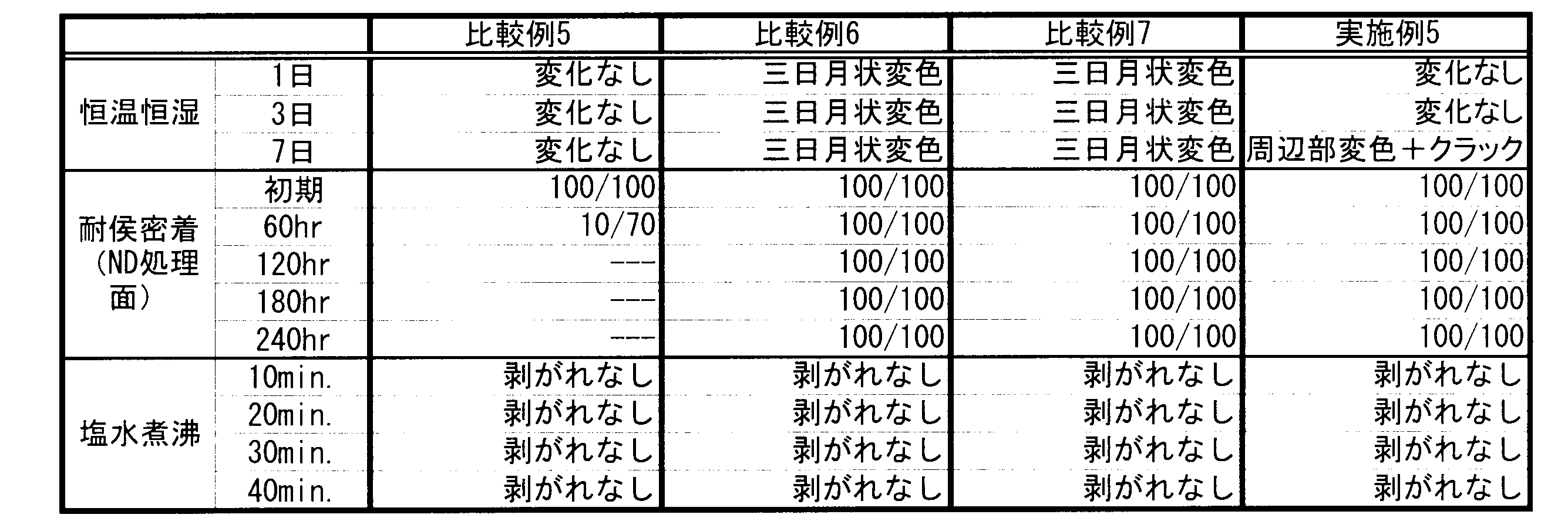
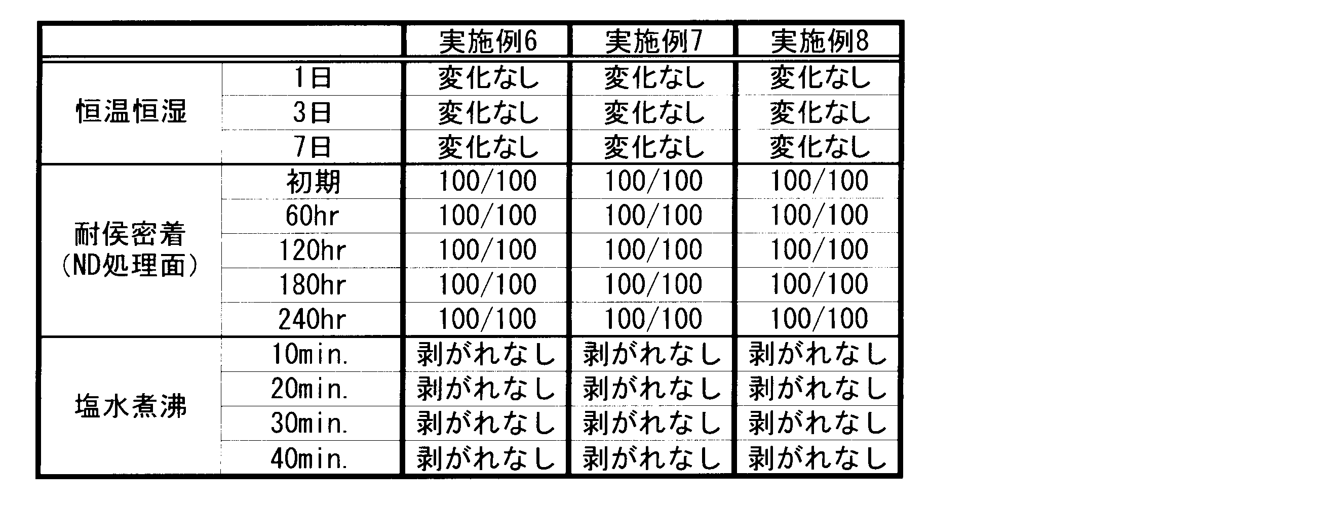
更に、実施例1~8では、恒温恒湿試験において、7日経過後も外観異常は観察されなかった(変化なし)。但し、実施例5では、3日経過の時点では外観異常は認められなかったが、7日経過後で周辺部変色とクラックの発生が認められた。
又、実施例1~8では、耐候密着試験において、全てのマスで剥がれが認められなかった(100/100)。
更に、実施例1~8では、恒温恒湿試験において、7日経過後も外観異常は観察されなかった(変化なし)。但し、実施例5では、3日経過の時点では外観異常は認められなかったが、7日経過後で周辺部変色とクラックの発生が認められた。
又、実施例1~8では、耐候密着試験において、全てのマスで剥がれが認められなかった(100/100)。
比較例1では、耐候密着試験において、120時間と180時間で計5回の剥がし完了後に1マス内の部分的な剥がれが認められたものの(99.5/100)、他に剥がれが認められず、良好な耐候性が示された。
しかし、恒温恒湿試験において、1日経過後において中心部の変色が認められ、3日経過後からはクラックの発生が認められた。
変色は、NiOx層において認められ、その様子から水分の作用によるものと考えられる。クラックは、凹面において発生しており、光吸収膜の応力バランスの状態に応じて発生するものと考えられる。
比較例1では、基材側から(以下同様)1層目がSiO2層やAl2O3層ではなくZrO2層である。ZrO2層は、SiO2層やAl2O3層に比べ、膜密度が小さすぎて水蒸気を通し易く、プラスチック基材からの水分がすぐに2層目以降に達して、特にNiOx層に影響し、変色を起こすものと考えられる。
1層目の膜密度向上の観点からは、実施例1~8の1層目がイオンアシストありで蒸着されるようにして密度が高められるようにすることが想定される。しかし、イオンアシストありの場合、密度が高すぎて水蒸気がほとんど通過しないこととなり(表6参照)、基材の水分は凹面において逃げ場を失って蓄積され、その蓄積量が限度を超えると水分が光吸収膜(1層目)の弱い部分から一点突破的に通過して、点状の外観異常を呈することとなる。これに対し、イオンアシストなしの場合、かような水分の蓄積ないし点状の外観異常が起こらない丁度良い密度となる。よって、1層目は、イオンアシストなしの状態に係る密度とされることが好ましい。
又、比較例1では、2つのNiOx層の基材側隣接層とその反対側の隣接層は、何れもSiO2+Al2O3混合層である。SiO2+Al2O3混合層は、SiO2層やAl2O3層に比べ、密度が比較的に高くなって水分を通し難い(緻密な構造となって高いパッキング効果を有する)。これは、SiO2をAl2O3が架橋することによるものと考えられる。
しかし、SiO2+Al2O3混合層は、NiOx層と応力が互いに異なり、NiOx層の応力とSiO2+Al2O3混合層の応力の差は比較的に大きい。よって、NiOx層の双方の隣接層ともSiO2+Al2O3混合層とすると、光吸収膜の応力バランスが比較的に良好ではなくなる。従って、恒温恒湿試験においてクラックが発生したものと考えられる。
これに対し、実施例1~5,7のように、少なくとも何れかのNiOx層において、基材側隣接層と反対側隣接層が互いに異なる材質とされれば、その異なる材質の層から応力が逃げて全体の応力が緩和されることとなり、クラックの発生が防止される。例えば、実施例1では、3層目のNiOx層の基材側隣接層である2層目のAl2O3層が、反対側隣接層である4層目のSiO2+Al2O3混合層と異なる材質であるため、その基材側隣接層から応力を逃がすことができる。5層目のNiOx層の基材側隣接層(4層目)と反対側隣接層(6層目)は、何れもSiO2+Al2O3混合層となるが、2層目のAl2O3層によって応力を緩和することができる。又、実施例2では、5層目のNiOx層の反対側隣接層である6層目のSiO2+Al2O3混合層が、基材側隣接層である4層目のAl2O3層と異なる材質であるため、その反対側隣接層から応力を逃がすことができる。
又、実施例6のCoOx’層や、実施例8のNiOx層及びCoOx’層の少なくとも一方においても、実施例1~5,7のNiOx層と同様に、少なくとも一つの光吸収層において基材側隣接層と反対側隣接層の材質を互いに相違させれば、応力が緩和され、クラックの発生が防止される。
尚、SiO2+Al2O3混合層におけるパッキング効果や応力差については、他のシリカ化合物においても同様な傾向となる。
比較例2では、耐候密着試験において、何れの時間であっても剥がれが認められず、良好な耐候性が示された。
しかし、恒温恒湿試験において、1日経過後において周辺部(端部)に極薄いシミ(変色)が認められ、7日経過後では端部のシミが濃くなっていると共に線状の変色が発生している状況が確認された。
比較例2における1層目のZrO2層はSiO2層やAl2O3層に比べ水分をより多く透過可能であるところ、プラスチック製の基材から放出される水分がその周辺部において2層目のNiOx層に達し、NiOx層を変性させたものと考えられる。
これに対し、実施例1~8では、光吸収膜の1層目がSiO2層又はAl2O3層であるため、ZrO2層ほど水分を通さず、NiOx層の水分による変性が防止される。尚、実施例1~8では、1層目のSiO2層又はAl2O3層がイオンアシストのない蒸着で形成される程度の密度であり、点状の変色の発生可能性がより低減され、より好ましい。
比較例3では、耐候密着試験において、何れの時間であっても剥がれが認められず、良好な耐候性が示された。
しかし、恒温恒湿試験において、1日経過後から全体的に線状の変色が発生し、7日経過後では更に中心部における変色箇所の増加が認められた。比較例3の光吸収膜の構成は、比較例2の1層目と2層目の間にSiO2層とZrO2層を加え、その分1層目のZrO2層の膜厚を薄くしたもの、即ち比較例2の1層目を3層に分割したものとなっているが、試験の結果を比較例2に比べて改善することはできず、よって1層目の分割を行っても、1層目がZrO2層であれば、NiOx層への水分透過の影響は防止することができないと考えられる。
しかし、恒温恒湿試験において、1日経過後から全体的に線状の変色が発生し、7日経過後では更に中心部における変色箇所の増加が認められた。比較例3の光吸収膜の構成は、比較例2の1層目と2層目の間にSiO2層とZrO2層を加え、その分1層目のZrO2層の膜厚を薄くしたもの、即ち比較例2の1層目を3層に分割したものとなっているが、試験の結果を比較例2に比べて改善することはできず、よって1層目の分割を行っても、1層目がZrO2層であれば、NiOx層への水分透過の影響は防止することができないと考えられる。
比較例4では、耐候密着試験において、初期から剥がれの有るマスが生じ、60時間において計5回の剥がし完了時に剥がれなしのマスが10マスしか残らなかったことから、その後の試験が中止された。
又、恒温恒湿試験において、1日経過後から中心部におけるクラックが認められた。
かように、比較例4は、耐候性や耐温性、耐湿性に乏しい。これは、比較例4が、比較例1と同様、何れのNiOx層もSiO2+Al2O3混合層で挟まれる構造を備えており、応力バランスが崩れた状態を保持していることによるものと考えられる。
尚、比較例4では変色の発生はなく、SiO2層が1層目であれば、NiOx層への水分の到達を防止できるものと考えられる。これに対し、比較例3では2層目にSiO2層が配置されるものの、1層目がZrO2層であるため、NiOx層への水分の到達を防止できない。
又、恒温恒湿試験において、1日経過後から中心部におけるクラックが認められた。
かように、比較例4は、耐候性や耐温性、耐湿性に乏しい。これは、比較例4が、比較例1と同様、何れのNiOx層もSiO2+Al2O3混合層で挟まれる構造を備えており、応力バランスが崩れた状態を保持していることによるものと考えられる。
尚、比較例4では変色の発生はなく、SiO2層が1層目であれば、NiOx層への水分の到達を防止できるものと考えられる。これに対し、比較例3では2層目にSiO2層が配置されるものの、1層目がZrO2層であるため、NiOx層への水分の到達を防止できない。
比較例5では、恒温恒湿試験では、7日経過後も外観異常は観察されなかった。
しかし、耐候密着試験では、60時間で多くの剥がれが認められた。
比較例5では、1層目がZrO2層であって水分をより透過し、又3層目と5層目のNiOx層が比較例1と同様にSiO2+Al2O3混合層で挟まれており、耐候性に影響がでたものと考えられる。
しかし、耐候密着試験では、60時間で多くの剥がれが認められた。
比較例5では、1層目がZrO2層であって水分をより透過し、又3層目と5層目のNiOx層が比較例1と同様にSiO2+Al2O3混合層で挟まれており、耐候性に影響がでたものと考えられる。
比較例6では、耐候密着試験において、何れの時間であっても剥がれが認められず、良好な耐候性が示された。
しかし、恒温恒湿試験において、1日経過後から、端部において三日月状の変色が認められた。
基材の凹面端部においては、蒸着時、NiOx(蒸着物質)の入射方向が基材の面の接線に対して垂直になっておらず、その垂直線から角度を持って傾いている。よって、NiOxの基材に対する入射方向が垂直である部分(中心部)に比べ、端部ではNiOx層におけるNiOxの密度が比較的に小さいものと考えられる。かようにNiOxの密度が小さいと、その分だけNiOx層が多孔質化し、多孔質化したNiOx層における孔部の断面積が閾値以上となると、孔部から水分が進入して、NiOx層が変質するようになる。比較例6では、可視光の吸収のためにNiOx層の膜厚が7.5nmとなっており、端部における多孔質化が比較的に顕著に現れて、主に大気側からの水分によりNiOx層が変性され、変色されるものと考えられる。
実施例1~5,7,8では、NiOx層の膜厚が4.2nm以上4.7nm以下となっており、端部における多孔質(ポーラス)化の影響が緩和されている。又、NiOx層の膜厚が薄ければ、隣接する層に対する応力の差がその分緩和される。実施例6,8のCoOx’層でも、同様に膜厚が4.5nm以下となっており、端部における多孔質化の影響が緩和されている。実施例1~8,比較例1~7、そしてシミュレーションの結果から、NiOx層やCoOx’層の膜厚が6nm以下であれば、多孔質化や応力差の緩和効果が良く発揮されることが分かった。NiOx層やCoOx’層を薄くすることにより可視光の吸収量が十分でなくなる場合には、(6nm以下の)層が複数設けられて良い(光吸収層の分割)。
比較例7では、比較例6と同様に、1日経過後から三日月状の変色が認められた。
比較例7では、NiOx層(6層目)の膜厚が比較的に大きく、更にNiOx層の基材側隣接層(5層目)と反対側隣接層(7層目)が何れもSiO2+Al2O3混合層であり、特に端部に応力差や多孔質化の影響が及んだものと考えられる。
比較例7では、NiOx層(6層目)の膜厚が比較的に大きく、更にNiOx層の基材側隣接層(5層目)と反対側隣接層(7層目)が何れもSiO2+Al2O3混合層であり、特に端部に応力差や多孔質化の影響が及んだものと考えられる。
以上の通り、実施例1~8のように、少なくとも一つの光吸収層(NiOx層及びCoOx’層の少なくとも一方で、複数層ある場合には少なくとも何れか1つの層)における基材側隣接層と、その反対側の隣接層とで、層の材質を相違させれば、基材がプラスチック製であり、耐久性に優れたNDフィルタを提供することができるのである。
Claims (8)
- プラスチックからなる基材と、
前記基材の少なくとも一面に配置された、複数の層を有する光吸収膜
を備えており、
前記光吸収膜における前記基材側から1層目の前記層は、SiO2からなるSiO2層又はAl2O3からなるAl2O3層であり、
前記光吸収膜は、NiOx(xは0以上1以下)からなるNiOx層及びCoOx’(x’は0以上1.5以下)からなるCoOx’層のうちの少なくとも何れか一方を1つ以上含んでおり、
前記NiOx層及び前記CoOx’層のうちの少なくとも何れか一方における少なくとも何れか1つは、基材側で隣接する前記層である基材側隣接層と、その反対側で隣接する前記層であって前記基材側隣接層と材質の異なる反対側隣接層とで挟まれている
ことを特徴とするプラスチック基材NDフィルタ。 - 前記NiOx層及びCoOx’層のうちの少なくとも一方は、何れも物理膜厚が6ナノメートル以下であるものとされている
ことを特徴とする請求項1に記載のプラスチック基材NDフィルタ。 - 前記基材側隣接層又は前記反対側隣接層は、シリカ化合物からなるシリカ化合物層である
ことを特徴とする請求項1又は請求項2に記載のプラスチック基材NDフィルタ。 - 前記SiO2層又は前記Al2O3層は、イオンアシストのない蒸着によって形成される程度の密度を有する
ことを特徴とする請求項1ないしは請求項3の何れかに記載のプラスチック基材NDフィルタ。 - 前記光吸収膜は、低屈折率層と高屈折率層が交互に配置されたものである
ことを特徴とする請求項1ないしは請求項4の何れかに記載のプラスチック基材NDフィルタ。 - 前記基材には、表面と裏面が存在しており、
前記光吸収膜は、前記裏面に配置されている
ことを特徴とする請求項1ないしは請求項5の何れかに記載のプラスチック基材NDフィルタ。 - 前記表面には、反射防止膜が配置されている
ことを特徴とする請求項6に記載のプラスチック基材NDフィルタ。 - 請求項1ないしは請求項7の何れかに記載されたプラスチック基材NDフィルタを含んでいる
ことを特徴とする眼鏡用プラスチック基材NDフィルタ。
Priority Applications (4)
| Application Number | Priority Date | Filing Date | Title |
|---|---|---|---|
| EP17756349.1A EP3407100B1 (en) | 2016-02-23 | 2017-02-16 | Nd filter with plastic base material, and nd filter with plastic base material for eyeglasses |
| KR1020187024298A KR102613927B1 (ko) | 2016-02-23 | 2017-02-16 | 플라스틱 기재 nd 필터 및 안경용 플라스틱 기재 nd 필터 |
| CN201780010020.9A CN108603952A (zh) | 2016-02-23 | 2017-02-16 | 塑料基材nd滤镜和眼镜用塑料基材nd滤镜 |
| US16/058,098 US10663634B2 (en) | 2016-02-23 | 2018-08-08 | ND filter with plastic base material, and ND filter with plastic base material for eyeglasses |
Applications Claiming Priority (2)
| Application Number | Priority Date | Filing Date | Title |
|---|---|---|---|
| JP2016032332 | 2016-02-23 | ||
| JP2016-032332 | 2016-02-23 |
Related Child Applications (1)
| Application Number | Title | Priority Date | Filing Date |
|---|---|---|---|
| US16/058,098 Continuation US10663634B2 (en) | 2016-02-23 | 2018-08-08 | ND filter with plastic base material, and ND filter with plastic base material for eyeglasses |
Publications (1)
| Publication Number | Publication Date |
|---|---|
| WO2017145910A1 true WO2017145910A1 (ja) | 2017-08-31 |
Family
ID=59685225
Family Applications (1)
| Application Number | Title | Priority Date | Filing Date |
|---|---|---|---|
| PCT/JP2017/005732 WO2017145910A1 (ja) | 2016-02-23 | 2017-02-16 | プラスチック基材ndフィルタ及び眼鏡用プラスチック基材ndフィルタ |
Country Status (6)
| Country | Link |
|---|---|
| US (1) | US10663634B2 (ja) |
| EP (1) | EP3407100B1 (ja) |
| JP (1) | JP6902775B2 (ja) |
| KR (1) | KR102613927B1 (ja) |
| CN (1) | CN108603952A (ja) |
| WO (1) | WO2017145910A1 (ja) |
Cited By (4)
| Publication number | Priority date | Publication date | Assignee | Title |
|---|---|---|---|---|
| CN109839346A (zh) * | 2017-11-26 | 2019-06-04 | 丹阳康斯特光学元件有限公司 | 一种镜片膜层牢固度检测方法 |
| JP2019133153A (ja) * | 2018-01-30 | 2019-08-08 | ヴァイアヴィ・ソリューションズ・インコーポレイテッドViavi Solutions Inc. | 光学的特性及び機械的特性を有する光学デバイス |
| WO2020250837A1 (ja) * | 2019-06-11 | 2020-12-17 | 東海光学株式会社 | プラスチック基材ndフィルタ及び眼鏡用プラスチック基材ndフィルタ |
| WO2021060554A1 (ja) * | 2019-09-28 | 2021-04-01 | ホヤ レンズ タイランド リミテッド | 眼鏡レンズ及び眼鏡レンズの製造方法 |
Families Citing this family (4)
| Publication number | Priority date | Publication date | Assignee | Title |
|---|---|---|---|---|
| US10429673B2 (en) * | 2017-09-11 | 2019-10-01 | Quantum Innovations, Inc. | High energy visible light absorbing material for ophthalmic substrate and application method |
| JP2020076883A (ja) * | 2018-11-08 | 2020-05-21 | 北川工業株式会社 | 反射防止フィルム |
| CN110068940B (zh) * | 2019-05-07 | 2020-07-28 | 河南达人视界眼镜有限公司 | 一种手机专用镜片 |
| CN110262079A (zh) * | 2019-07-19 | 2019-09-20 | 厦门美澜光电科技有限公司 | 一种埃米抗氧化渐进多彩镜片及其制备方法 |
Citations (8)
| Publication number | Priority date | Publication date | Assignee | Title |
|---|---|---|---|---|
| JP2003043211A (ja) * | 2001-07-27 | 2003-02-13 | Nidec Copal Corp | 薄膜型ndフィルタ及びその製造方法 |
| WO2005047940A1 (ja) * | 2003-11-14 | 2005-05-26 | Nidec Copal Corporation | Ndフィルタ及びこれを用いた光量絞り装置 |
| JP2009157211A (ja) * | 2007-12-27 | 2009-07-16 | Shincron:Kk | 光学フィルター及びその製造方法並びに該光学フィルターを備えた光学機器 |
| JP2009162852A (ja) * | 2007-12-28 | 2009-07-23 | Canon Electronics Inc | 光学素子 |
| JP2011002515A (ja) * | 2009-06-16 | 2011-01-06 | Tokai Kogaku Kk | 光学製品及び眼鏡プラスチックレンズ |
| JP5066644B2 (ja) | 2008-04-30 | 2012-11-07 | 東海光学株式会社 | 多層膜ndフィルター |
| JP2014002270A (ja) * | 2012-06-19 | 2014-01-09 | Tokai Kogaku Kk | カメラ用ndフィルタ及びその製造方法 |
| US20140154769A1 (en) * | 2012-12-03 | 2014-06-05 | Wave Tech, LLC | Optical filter, production system using the optical filter, and method of using the optical filter |
Family Cites Families (6)
| Publication number | Priority date | Publication date | Assignee | Title |
|---|---|---|---|---|
| JP3991671B2 (ja) * | 2001-12-11 | 2007-10-17 | 凸版印刷株式会社 | 積層体 |
| JP4481720B2 (ja) * | 2004-05-14 | 2010-06-16 | 日本電産コパル株式会社 | Ndフィルタ及び光量絞り装置 |
| JP4595687B2 (ja) * | 2004-07-20 | 2010-12-08 | 住友金属鉱山株式会社 | 吸収型多層膜ndフィルター |
| JP2006084994A (ja) * | 2004-09-17 | 2006-03-30 | Nidec Copal Corp | Ndフィルタ及びこれを用いた光量絞り装置 |
| JP4613706B2 (ja) * | 2004-11-24 | 2011-01-19 | 住友金属鉱山株式会社 | 吸収型多層膜ndフィルター |
| TWI487932B (zh) * | 2013-11-21 | 2015-06-11 | Global Wafers Co Ltd | 光學元件及其製造方法 |
-
2017
- 2017-02-16 CN CN201780010020.9A patent/CN108603952A/zh active Pending
- 2017-02-16 EP EP17756349.1A patent/EP3407100B1/en active Active
- 2017-02-16 WO PCT/JP2017/005732 patent/WO2017145910A1/ja active Application Filing
- 2017-02-16 JP JP2017027198A patent/JP6902775B2/ja active Active
- 2017-02-16 KR KR1020187024298A patent/KR102613927B1/ko active IP Right Grant
-
2018
- 2018-08-08 US US16/058,098 patent/US10663634B2/en active Active
Patent Citations (8)
| Publication number | Priority date | Publication date | Assignee | Title |
|---|---|---|---|---|
| JP2003043211A (ja) * | 2001-07-27 | 2003-02-13 | Nidec Copal Corp | 薄膜型ndフィルタ及びその製造方法 |
| WO2005047940A1 (ja) * | 2003-11-14 | 2005-05-26 | Nidec Copal Corporation | Ndフィルタ及びこれを用いた光量絞り装置 |
| JP2009157211A (ja) * | 2007-12-27 | 2009-07-16 | Shincron:Kk | 光学フィルター及びその製造方法並びに該光学フィルターを備えた光学機器 |
| JP2009162852A (ja) * | 2007-12-28 | 2009-07-23 | Canon Electronics Inc | 光学素子 |
| JP5066644B2 (ja) | 2008-04-30 | 2012-11-07 | 東海光学株式会社 | 多層膜ndフィルター |
| JP2011002515A (ja) * | 2009-06-16 | 2011-01-06 | Tokai Kogaku Kk | 光学製品及び眼鏡プラスチックレンズ |
| JP2014002270A (ja) * | 2012-06-19 | 2014-01-09 | Tokai Kogaku Kk | カメラ用ndフィルタ及びその製造方法 |
| US20140154769A1 (en) * | 2012-12-03 | 2014-06-05 | Wave Tech, LLC | Optical filter, production system using the optical filter, and method of using the optical filter |
Non-Patent Citations (1)
| Title |
|---|
| See also references of EP3407100A4 |
Cited By (7)
| Publication number | Priority date | Publication date | Assignee | Title |
|---|---|---|---|---|
| CN109839346A (zh) * | 2017-11-26 | 2019-06-04 | 丹阳康斯特光学元件有限公司 | 一种镜片膜层牢固度检测方法 |
| JP2019133153A (ja) * | 2018-01-30 | 2019-08-08 | ヴァイアヴィ・ソリューションズ・インコーポレイテッドViavi Solutions Inc. | 光学的特性及び機械的特性を有する光学デバイス |
| US11360242B2 (en) | 2018-01-30 | 2022-06-14 | Viavi Solutions Inc. | Optical device having optical and mechanical properties |
| WO2020250837A1 (ja) * | 2019-06-11 | 2020-12-17 | 東海光学株式会社 | プラスチック基材ndフィルタ及び眼鏡用プラスチック基材ndフィルタ |
| JP2020201412A (ja) * | 2019-06-11 | 2020-12-17 | 東海光学株式会社 | プラスチック基材ndフィルタ及び眼鏡用プラスチック基材ndフィルタ |
| JP7385894B2 (ja) | 2019-06-11 | 2023-11-24 | 東海光学株式会社 | プラスチック基材ndフィルタ及び眼鏡用プラスチック基材ndフィルタ |
| WO2021060554A1 (ja) * | 2019-09-28 | 2021-04-01 | ホヤ レンズ タイランド リミテッド | 眼鏡レンズ及び眼鏡レンズの製造方法 |
Also Published As
| Publication number | Publication date |
|---|---|
| US20180348414A1 (en) | 2018-12-06 |
| KR102613927B1 (ko) | 2023-12-15 |
| JP6902775B2 (ja) | 2021-07-14 |
| CN108603952A (zh) | 2018-09-28 |
| US10663634B2 (en) | 2020-05-26 |
| EP3407100A4 (en) | 2019-10-02 |
| KR20180114071A (ko) | 2018-10-17 |
| EP3407100A1 (en) | 2018-11-28 |
| JP2017151430A (ja) | 2017-08-31 |
| EP3407100B1 (en) | 2023-12-20 |
Similar Documents
| Publication | Publication Date | Title |
|---|---|---|
| WO2017145910A1 (ja) | プラスチック基材ndフィルタ及び眼鏡用プラスチック基材ndフィルタ | |
| ES2893349T3 (es) | Artículo óptico que comprende un revestimiento anti-reflectante con una reflexión muy baja en las regiones visible y ultravioleta | |
| KR101910950B1 (ko) | 가시 영역에서 매우 낮은 반사를 갖는 반사 방지 코팅을 포함하는 광학 물품 | |
| US10031349B2 (en) | Optical product, and spectacle lens and spectacles | |
| US8908275B2 (en) | Optical product and spectacle plastic lens | |
| CN107111000B (zh) | 包括在紫外区域具有高反射率的干涉涂层的光学物品 | |
| DE202011110943U1 (de) | Optischer Gegenstand mit einer Antireflexionsbeschichtung mit niedriger Reflexion sowohl im ultravioletten Bereich als auch im sichtbaren Bereich | |
| BR112014028470B1 (pt) | Lente oftálmica e vidro de óculos constituído por uma lente oftálmica | |
| JP2019515352A (ja) | 近赤外領域(nir)において高反射率を有する反射防止膜を含む光学物品 | |
| WO2014208412A1 (ja) | 光学部品 | |
| US10234697B2 (en) | Composite high index layers for anti reflective stacks | |
| KR20120002577A (ko) | 광학 부재, 안경용 플라스틱 렌즈 및 그것들의 제조 방법 | |
| WO2015030246A1 (ja) | 眼鏡レンズ | |
| KR20180078328A (ko) | 안경 렌즈 및 안경 | |
| EP3581675A1 (en) | Optical article having directional micro- or nanostructured thin film coating, and its process | |
| JP2021531511A (ja) | 反射防止機能及びエレクトロクロミック機能を有する眼用レンズ | |
| JP7385894B2 (ja) | プラスチック基材ndフィルタ及び眼鏡用プラスチック基材ndフィルタ | |
| CN115427841A (zh) | 包含吸光化合物的光学制品及相应的制造方法 | |
| CN117377891A (zh) | 具有改善的视觉舒适度的光学制品 | |
| KR20210032855A (ko) | 청광 차단 저반사 광학부재 및 이의 제조방법 |
Legal Events
| Date | Code | Title | Description |
|---|---|---|---|
| WWE | Wipo information: entry into national phase |
Ref document number: 2017756349 Country of ref document: EP |
|
| NENP | Non-entry into the national phase |
Ref country code: DE |
|
| ENP | Entry into the national phase |
Ref document number: 2017756349 Country of ref document: EP Effective date: 20180820 |
|
| 121 | Ep: the epo has been informed by wipo that ep was designated in this application |
Ref document number: 17756349 Country of ref document: EP Kind code of ref document: A1 |