WO2017134919A1 - シリコンウェーハの片面研磨方法 - Google Patents
シリコンウェーハの片面研磨方法 Download PDFInfo
- Publication number
- WO2017134919A1 WO2017134919A1 PCT/JP2016/085929 JP2016085929W WO2017134919A1 WO 2017134919 A1 WO2017134919 A1 WO 2017134919A1 JP 2016085929 W JP2016085929 W JP 2016085929W WO 2017134919 A1 WO2017134919 A1 WO 2017134919A1
- Authority
- WO
- WIPO (PCT)
- Prior art keywords
- polishing
- silicon wafer
- silicon
- rate
- condition
- Prior art date
- Legal status (The legal status is an assumption and is not a legal conclusion. Google has not performed a legal analysis and makes no representation as to the accuracy of the status listed.)
- Ceased
Links
Images


Classifications
-
- H—ELECTRICITY
- H10—SEMICONDUCTOR DEVICES; ELECTRIC SOLID-STATE DEVICES NOT OTHERWISE PROVIDED FOR
- H10P—GENERIC PROCESSES OR APPARATUS FOR THE MANUFACTURE OR TREATMENT OF DEVICES COVERED BY CLASS H10
- H10P52/00—Grinding, lapping or polishing of wafers, substrates or parts of devices
-
- B—PERFORMING OPERATIONS; TRANSPORTING
- B24—GRINDING; POLISHING
- B24B—MACHINES, DEVICES, OR PROCESSES FOR GRINDING OR POLISHING; DRESSING OR CONDITIONING OF ABRADING SURFACES; FEEDING OF GRINDING, POLISHING, OR LAPPING AGENTS
- B24B37/00—Lapping machines or devices; Accessories
- B24B37/04—Lapping machines or devices; Accessories designed for working plane surfaces
- B24B37/07—Lapping machines or devices; Accessories designed for working plane surfaces characterised by the movement of the work or lapping tool
- B24B37/10—Lapping machines or devices; Accessories designed for working plane surfaces characterised by the movement of the work or lapping tool for single side lapping
- B24B37/105—Lapping machines or devices; Accessories designed for working plane surfaces characterised by the movement of the work or lapping tool for single side lapping the workpieces or work carriers being actively moved by a drive, e.g. in a combined rotary and translatory movement
- B24B37/107—Lapping machines or devices; Accessories designed for working plane surfaces characterised by the movement of the work or lapping tool for single side lapping the workpieces or work carriers being actively moved by a drive, e.g. in a combined rotary and translatory movement in a rotary movement only, about an axis being stationary during lapping
-
- B—PERFORMING OPERATIONS; TRANSPORTING
- B24—GRINDING; POLISHING
- B24B—MACHINES, DEVICES, OR PROCESSES FOR GRINDING OR POLISHING; DRESSING OR CONDITIONING OF ABRADING SURFACES; FEEDING OF GRINDING, POLISHING, OR LAPPING AGENTS
- B24B37/00—Lapping machines or devices; Accessories
- B24B37/04—Lapping machines or devices; Accessories designed for working plane surfaces
- B24B37/042—Lapping machines or devices; Accessories designed for working plane surfaces operating processes therefor
-
- B—PERFORMING OPERATIONS; TRANSPORTING
- B24—GRINDING; POLISHING
- B24B—MACHINES, DEVICES, OR PROCESSES FOR GRINDING OR POLISHING; DRESSING OR CONDITIONING OF ABRADING SURFACES; FEEDING OF GRINDING, POLISHING, OR LAPPING AGENTS
- B24B37/00—Lapping machines or devices; Accessories
- B24B37/04—Lapping machines or devices; Accessories designed for working plane surfaces
- B24B37/07—Lapping machines or devices; Accessories designed for working plane surfaces characterised by the movement of the work or lapping tool
- B24B37/10—Lapping machines or devices; Accessories designed for working plane surfaces characterised by the movement of the work or lapping tool for single side lapping
-
- B—PERFORMING OPERATIONS; TRANSPORTING
- B24—GRINDING; POLISHING
- B24B—MACHINES, DEVICES, OR PROCESSES FOR GRINDING OR POLISHING; DRESSING OR CONDITIONING OF ABRADING SURFACES; FEEDING OF GRINDING, POLISHING, OR LAPPING AGENTS
- B24B37/00—Lapping machines or devices; Accessories
- B24B37/04—Lapping machines or devices; Accessories designed for working plane surfaces
- B24B37/07—Lapping machines or devices; Accessories designed for working plane surfaces characterised by the movement of the work or lapping tool
- B24B37/10—Lapping machines or devices; Accessories designed for working plane surfaces characterised by the movement of the work or lapping tool for single side lapping
- B24B37/105—Lapping machines or devices; Accessories designed for working plane surfaces characterised by the movement of the work or lapping tool for single side lapping the workpieces or work carriers being actively moved by a drive, e.g. in a combined rotary and translatory movement
-
- B—PERFORMING OPERATIONS; TRANSPORTING
- B24—GRINDING; POLISHING
- B24B—MACHINES, DEVICES, OR PROCESSES FOR GRINDING OR POLISHING; DRESSING OR CONDITIONING OF ABRADING SURFACES; FEEDING OF GRINDING, POLISHING, OR LAPPING AGENTS
- B24B51/00—Arrangements for automatic control of a series of individual steps in grinding a workpiece
-
- H—ELECTRICITY
- H10—SEMICONDUCTOR DEVICES; ELECTRIC SOLID-STATE DEVICES NOT OTHERWISE PROVIDED FOR
- H10P—GENERIC PROCESSES OR APPARATUS FOR THE MANUFACTURE OR TREATMENT OF DEVICES COVERED BY CLASS H10
- H10P52/00—Grinding, lapping or polishing of wafers, substrates or parts of devices
- H10P52/40—Chemomechanical polishing [CMP]
- H10P52/402—Chemomechanical polishing [CMP] of semiconductor materials
-
- H—ELECTRICITY
- H10—SEMICONDUCTOR DEVICES; ELECTRIC SOLID-STATE DEVICES NOT OTHERWISE PROVIDED FOR
- H10P—GENERIC PROCESSES OR APPARATUS FOR THE MANUFACTURE OR TREATMENT OF DEVICES COVERED BY CLASS H10
- H10P90/00—Preparation of wafers not covered by a single main group of this subclass, e.g. wafer reinforcement
- H10P90/12—Preparing bulk and homogeneous wafers
- H10P90/129—Preparing bulk and homogeneous wafers by polishing
-
- H—ELECTRICITY
- H10—SEMICONDUCTOR DEVICES; ELECTRIC SOLID-STATE DEVICES NOT OTHERWISE PROVIDED FOR
- H10P—GENERIC PROCESSES OR APPARATUS FOR THE MANUFACTURE OR TREATMENT OF DEVICES COVERED BY CLASS H10
- H10P95/00—Generic processes or apparatus for manufacture or treatments not covered by the other groups of this subclass
- H10P95/04—Planarisation of conductive or resistive materials
-
- H—ELECTRICITY
- H10—SEMICONDUCTOR DEVICES; ELECTRIC SOLID-STATE DEVICES NOT OTHERWISE PROVIDED FOR
- H10P—GENERIC PROCESSES OR APPARATUS FOR THE MANUFACTURE OR TREATMENT OF DEVICES COVERED BY CLASS H10
- H10P95/00—Generic processes or apparatus for manufacture or treatments not covered by the other groups of this subclass
- H10P95/06—Planarisation of inorganic insulating materials
-
- H—ELECTRICITY
- H10—SEMICONDUCTOR DEVICES; ELECTRIC SOLID-STATE DEVICES NOT OTHERWISE PROVIDED FOR
- H10P—GENERIC PROCESSES OR APPARATUS FOR THE MANUFACTURE OR TREATMENT OF DEVICES COVERED BY CLASS H10
- H10P95/00—Generic processes or apparatus for manufacture or treatments not covered by the other groups of this subclass
- H10P95/06—Planarisation of inorganic insulating materials
- H10P95/062—Planarisation of inorganic insulating materials involving a dielectric removal step
-
- B—PERFORMING OPERATIONS; TRANSPORTING
- B24—GRINDING; POLISHING
- B24B—MACHINES, DEVICES, OR PROCESSES FOR GRINDING OR POLISHING; DRESSING OR CONDITIONING OF ABRADING SURFACES; FEEDING OF GRINDING, POLISHING, OR LAPPING AGENTS
- B24B37/00—Lapping machines or devices; Accessories
- B24B37/005—Control means for lapping machines or devices
- B24B37/0053—Control means for lapping machines or devices detecting loss or breakage of a workpiece during lapping
Definitions
- the present invention relates to a method for polishing a single side of a silicon wafer.
- Semiconductor wafer surface polishing methods that require high flatness such as silicon wafers, are broadly divided into double-side polishing methods that simultaneously polish both surfaces of a semiconductor wafer and single-side polishing methods that polish only one surface.
- the single-side polishing method is widely used from rough polishing using a relatively hard polishing cloth to finish polishing using a relatively soft polishing cloth.
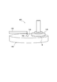
- the single-side polishing apparatus 100 includes a polishing head 120 that holds a semiconductor wafer W and a rotating surface plate 140 to which a polishing cloth 130 is attached.
- the single-side polishing apparatus 100 includes a rotating mechanism that rotates the polishing head 120 and a moving mechanism that moves the polishing head 120 in and out of the rotating surface plate 140.
- the polishing head 120 holds the semiconductor wafer W and holds the surface of the semiconductor wafer W to be polished (that is, the surface on the surface plate 140 side) with respect to the polishing cloth 130 attached to the upper surface of the rotating surface plate 140.
- DIC differential interference contrast
- a laser L for example, a He—Ne laser
- the photodiode P receives the reflected light reflected from the surface of the semiconductor wafer W via the mirror M.
- a phase difference peculiar to the stepped micro defect is detected, and height information of the defect can be obtained from the optical path difference of the reflected light.
- a stepped microdefect having a concavo-convex shape detected by the DIC method and having a height threshold value exceeding 3.4 nm, which is particularly problematic at present is simply referred to as a “stepped microdefect”.
- the number of stepped micro defects is within a desired standard, it can be determined that the quality of the surface of the silicon wafer after finish polishing is good. On the other hand, since a silicon wafer that does not satisfy the desired standard is determined as a defective product, such a silicon wafer cannot be shipped as a product.
- the rate of occurrence of stepped micro defects on the surface of the silicon wafer after finish polishing is not always satisfactory, and further improvement of the single-side polishing method is required in order to improve the product yield.
- an object of the present invention is to provide a silicon wafer single-side polishing method capable of greatly improving the incidence of stepped micro defects.
- the silicon wafer when performing final polishing of a silicon wafer, the silicon wafer is in a naturally oxidized state. That is, the silicon wafer is composed of bare silicon (part without a natural oxide film: Bare Silicon) and a silicon oxide film (generally a natural oxide film) that covers the surface of the silicon wafer. From this state, single-side polishing of the silicon wafer is started. In the single-side polishing method, it is difficult to completely prevent the occurrence of polishing unevenness in the silicon wafer surface, and there is a moment when a portion where the silicon oxide film is removed by polishing and a portion where the silicon oxide film remains are mixed. (See FIG. 4B described later).
- the silicon oxide film is removed by chemical mechanical polishing, but most is removed by the contribution of mechanical polishing.
- both chemical polishing and mechanical polishing contribute to bare silicon polishing. Therefore, in the single-side polishing of a silicon wafer, the polishing rate of silicon oxide is generally smaller than the polishing rate of silicon. After the above-mentioned mixed state occurs, the remaining silicon oxide film is continuously polished and removed, but bare silicon polishing proceeds rapidly in the portion where the silicon oxide film has already been polished and removed. The present inventors thought that it would become a fine defect.
- the present inventors studied to perform single-side polishing under the condition that the polishing rate of silicon oxide was increased.
- the contribution of mechanical polishing is the center, it is conceivable that not only the bare silicon polishing rate is lowered, but also the polishing sag at the periphery of the silicon wafer is increased.
- the inventors of the present invention can greatly improve the incidence of stepped micro defects by first performing polishing for removing the silicon oxide film and then performing polishing for final polishing of silicon.
- the present invention has been completed. That is, the gist configuration of the present invention is as follows.
- a silicon wafer with a silicon oxide film formed on a bare silicon surface is held by a polishing head, and the silicon wafer is pressed against a rotating surface plate to which a polishing cloth is attached while rotating the silicon wafer.
- the silicon wafer single-side polishing method for polishing one side of the rotating surface plate side is characterized in that the silicon wafer is subjected to the first polishing condition relating to the pressure applied to the silicon wafer and the relative speed of the silicon wafer and the rotating surface plate.
- a second polishing step of polishing the one side, and polishing the silicon under the first polishing conditions The polishing rate ratio of the silicon oxide polishing rate for over preparative is, and greater than the polishing rate ratio of the silicon oxide polishing rate for silicon polishing rate by the second polishing conditions.
- the polishing rate ratio according to the first polishing condition is preferably 0.5 or more.
- it is preferable that the polishing rate ratio according to the second polishing condition is less than 0.5.
- the first polishing step and the second polishing step are performed according to the polishing conditions in which the polishing rate ratio of the silicon oxide polishing rate to the silicon polishing rate is changed, the occurrence rate of stepped micro defects can be greatly improved. It is possible to provide a method for polishing a single side of a silicon wafer.
- FIG. 1 It is a schematic diagram explaining the single-sided polishing method of the semiconductor wafer in a prior art. It is a schematic diagram explaining the measurement principle of the step-shaped micro defect by the differential interference contrast method in a prior art. It is a schematic cross section for demonstrating the grinding
- FIG. 1 is a graph showing an example of the polishing rate of each of silicon and silicon oxide for explaining an embodiment of the present invention
- (A) is a graph showing the polishing rate with respect to applied pressure
- (B) is a relative speed. It is a graph which shows the polishing rate with respect to. It is a graph for demonstrating the generation
- FIGS. 1-10 Single-side polishing method A method for polishing a single side of a silicon wafer according to an embodiment of the present invention will be described with reference to FIGS.
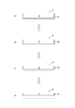
- the silicon wafer W formed on the surface of the bare silicon 10 with the silicon oxide film 20 is held by a polishing head, and the silicon wafer W is rotated on a rotating surface plate to which a polishing cloth is attached. By pressing, one surface of the silicon wafer W on the rotating surface plate side is polished.
- This single-side polishing can be performed according to a conventional method using a general single-side polishing apparatus.
- the polishing surface 120 of the silicon wafer W (that is, the rotation constant) is fixed to the polishing cloth 130 attached to the upper surface of the rotating surface plate 140 while the polishing head 120 holds the silicon wafer W.
- the polishing head 120 and the rotating surface plate 140 are rotated together to cause the polishing head 120 and the rotating surface plate 140 to move relative to each other, thereby supplying the polishing liquid 160 from the polishing liquid supply means 150.
- single-side polishing can be performed by chemical mechanical polishing only the surface to be polished of the silicon wafer W.
- FIG. 1 shows single-wafer single-side polishing in which only one silicon wafer W is polished, batch-type single-side polishing in which a plurality of wafers are simultaneously polished on one side may be used.
- the single-side polishing method polishes the single side of the silicon wafer W according to the first polishing condition relating to the pressing force for pressing the silicon wafer W and the relative speed of the silicon wafer W and the rotary platen.
- a first polishing step (FIGS. 3A and 3B) and a second polishing condition in which at least one of the applied pressure and the relative speed in the first polishing condition is changed after the first polishing step.
- a second polishing step (FIGS. 3C and 3D) for polishing the one surface of the silicon wafer W is included.
- the reason why the first and second polishing conditions relate to the pressing force and the relative speed is that the pressing force and the relative speed are the silicon polishing rate (hereinafter referred to as “Si polishing rate”) and the silicon oxide polishing rate (hereinafter referred to as “SiO 2”). This is because it particularly affects each of “ 2 polishing rates”.
- Si polishing rate silicon polishing rate
- SiO 2 silicon oxide polishing rate
- the polishing rate ratio of the SiO 2 polishing rate to the Si polishing rate under the first polishing condition (hereinafter referred to as “SiO 2 / Si polishing rate ratio”) is the SiO 2 / Si polishing rate under the subsequent second polishing condition. It is important in the present embodiment that the ratio is larger than the ratio. By passing through this process, it is possible to greatly improve the occurrence rate of stepped micro defects on the polished silicon wafer surface. Hereinafter, each step will be described.
- the polishing conditions related to the pressure applied to the silicon wafer W and the relative speed of the silicon wafer W and the rotating surface plate when polishing the silicon wafer W are defined as the first polishing condition.
- This first polishing step is polishing whose main purpose is to remove the silicon oxide film 20 by polishing. The details of the first polishing condition will be described later together with the second polishing condition.
- the relative speed is determined by the rotation speed of the rotary platen 140 and the rotation speed of the silicon wafer W by the polishing head 120, and if at least one of the rotation speeds is changed. The relative speed also changes.
- the relative speed is determined by the rotational speeds of the polishing head and the rotating surface plate.
- the first polishing conditions include the type of slurry (particle size, concentration, pH, etc.) and its supply temperature, and the material of the polishing cloth, the hole diameter and the opening ratio, etc. It may be included.
- the second polishing condition can include the type of slurry and its supply temperature, the material of the polishing cloth, the hole diameter, the opening ratio, and the like in addition to the applied pressure and the relative speed. .
- the one surface of the silicon wafer W is polished following the first polishing step.
- This second polishing step is polishing mainly intended for polishing bare silicon 10 after the silicon oxide film 20 has already been removed.
- the SiO 2 / Si polishing rate ratio of the first polishing conditions larger than SiO 2 / Si polishing rate ratio of the second polishing conditions.
- the SiO 2 / Si polishing rate ratio under the second polishing condition is made smaller than the SiO 2 / Si polishing rate ratio under the first polishing condition.
- the SiO 2 / Si polishing rate ratio of the first polishing conditions as described above, larger than SiO 2 / Si polishing rate ratio of the second polishing conditions explain the technical significance of doing this.
- the bare silicon 10 is polished by the second polishing process.
- the occurrence rate of minute defects can be greatly improved. This effect can be understood more clearly by comparing with the single-side polishing method in the prior art shown in FIGS. 4A to 4C, as will be described below.
- FIGS. 4A to 4C schematically show the polishing process.
- the prior art attention was not paid to the generation of stepped micro defects, but only the polishing of bare silicon 10 was focused on, so single-side polishing was performed with a constant SiO 2 / Si polishing rate ratio. .
- the conventional polishing conditions it was common to make the SiO 2 / Si polishing rate ratio relatively small.
- FIG. 4B when the silicon oxide film 20B and bare silicon 10 are mixed in the surface on the polishing side (FIG. 4B), the subsequent polishing is performed.
- a step-like minute defect D2 can be detected by a DIC method using a commercially available wafer surface inspection apparatus.
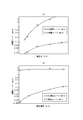
- FIG. 5 (A) is an example of a graph showing the polishing rate with respect to the applied pressure when only the applied pressure is changed in a predetermined single-side polishing apparatus.
- the polishing conditions other than the pressure are the same.
- the horizontal axis is an arbitrary unit (AU).
- the SiO 2 polishing rate and the Si polishing rate both decrease as the pressing force decreases, and the SiO 2 polishing rate and the Si polishing rate tend to increase as the pressing force increases.
- the rate of change between the SiO 2 polishing rate and the Si polishing rate is different between the two, and the lower the applied pressure, the closer the polishing rate of both, and the lower the applied pressure, the higher the SiO 2 / Si polishing rate ratio tends to be.
- FIG. This is probably because the smaller the applied pressure, the smaller the contribution of the chemical polishing action.
- FIG. 5B is an example of a graph showing the polishing rate relative to the relative speed between the silicon wafer and the rotating platen when only the relative speed is changed in the single-side polishing apparatus, and the relative speed such as the applied pressure.
- the polishing conditions other than are the same.
- the horizontal axis is an arbitrary unit (AU).
- AU arbitrary unit
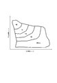
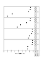
- each of the SiO 2 polishing rate and the Si polishing rate is uniquely determined, and the SiO 2 / Si polishing rate ratio is also uniquely determined. Therefore, the relationship between the generation rate of the stepped micro defects (occurrence number rate) and the first polishing condition will be described using the graph shown in FIG.
- the numerical values shown in each area in FIG. 6 indicate the number of defects in which step-shaped micro defects are generated with a probability of a predetermined threshold (for example, 90%). “0” means that the step-shaped micro defect does not occur with the probability of the predetermined threshold.
- a predetermined threshold for example, 90%
- Each of the SiO 2 polishing rate and the Si polishing rate can vary greatly depending on the specifications of the single-side polishing apparatus, the material of the polishing pad, the type of silicon wafer, etc. in addition to the applied pressure and the relative speed, It is considered that the generation rate of sigma greatly depends on the SiO 2 / Si polishing rate ratio.
- the present inventors have focused on the SiO 2 / Si polishing rate ratio, the SiO 2 / Si polishing rate ratio of the first polishing conditions, to be larger than SiO 2 / Si polishing rate ratio of the second polishing conditions The inventors have conceived and experimentally clarified the effect.
- the removal of the silicon oxide film 20 referred to here means the removal of the portion of the silicon oxide film 20 covering the main surface of the bare silicon 10 as shown in FIGS. 3A and 3B. It will be understood that the removal of the silicon oxide film 20A on the side surface of the silicon 10 is not intended.
- the first polishing step can be performed only for the time (or by adding a predetermined time to the time).
- the removal of the silicon oxide film may be detected using the torque of a motor that drives a rotating platen or polishing head in a single-side polishing apparatus, and the second step may be performed after the detection.
- the occurrence rate of the stepped micro defects can be greatly improved as compared with the prior art only by appropriately setting the time for performing the first polishing process as desired.
- the SiO 2 / Si polishing rate ratio according to the first polishing condition is preferably 0.5 or more, and the SiO 2 / Si polishing rate ratio may be further increased. In this case, it is possible to remarkably reduce the number ratio at which step-like micro defects are generated.
- the upper limit of the SiO 2 / Si polishing rate ratio is not particularly limited.
- the SiO 2 / Si polishing rate ratio according to the second polishing condition is preferably less than 0.5.
- the SiO 2 / Si polishing rate ratio can be appropriately set within this range.
- the present invention can be applied to any silicon wafer as long as the bulk silicon substrate surface is naturally oxidized to form a silicon oxide film, and the size and thickness of the silicon wafer are not limited at all.
- a single-side polishing interruption step for changing the polishing conditions may be included in the present embodiment between the first polishing step and the second polishing step, or single-side polishing may be performed while gradually changing the polishing conditions.
- An advanced polishing condition adjustment step may be included in this embodiment.
- a cleaning step with pure water or the like may be performed.
- the single-side polishing method according to the present embodiment is particularly suitable for use in final polishing in which single-side polishing is performed using a relatively soft polishing cloth such as a suede material.
- the rotation speed (rpm) of the polishing head and the rotating platen is 16, 24, 43, 55, and the pressure (g / cm 2 ) is 50, 60, It was changed to 100, 150, 200.
- Example 1 The first polishing step and the second polishing step were performed on the same type of silicon wafer as used in the preliminary experimental example under the polishing conditions shown in Table 1 below. Further, after the second polishing step, a silicon wafer cleaning step after polishing with pure water was performed. Other conditions were the same as in the preliminary experimental example, and single-side polishing of 100 silicon wafers was performed. In Table 1, the SiO 2 / Si polishing rate ratio is simply described as “polishing rate ratio”. In addition, since the SiO 2 polishing rate in the first polishing step is 1 nm / min, it may be considered that all of the silicon oxide film has been removed by polishing for 60 seconds.
- the SiO 2 / Si polishing rate ratio is different between the first polishing step and the second polishing step, but the first polishing step is low pressure and high speed rotation, and the second polishing step is high pressure and low speed rotation. Therefore, the SiO 2 polishing rate in both polishing steps was almost the same.
- Example 2 One-side polishing of 100 silicon wafers was performed in the same manner as in Example 1 except that the rotational speed of the first polishing process in Example 1 was changed to set the SiO 2 / Si polishing rate ratio to 0.3. .
- Example 3 One-side polishing of 100 silicon wafers was performed in the same manner as in Example 1 except that the rotational speed of the first polishing process in Example 1 was changed to set the SiO 2 / Si polishing rate ratio to 0.1. .
- Example 1 The polished surface of each silicon wafer according to Example 1 and Conventional Example 1 was measured in the DIC mode (measurement mode by the DIC method) using a wafer surface inspection apparatus (Surfscan SP2; manufactured by KLA-Tencor).
- the threshold value of the height of the uneven stepped micro defect was set to 3.4 nm, and the number of stepped micro defects exceeding the threshold value was obtained.
- the number of silicon wafers in which the number of defects detected by the DIC method was zero was confirmed in Example 1 and Conventional Example 1.
- Example 1 the occurrence of stepped micro defects was not confirmed in 93 out of 100 sheets, whereas in Conventional Example 1, the generation of stepped micro defects was not confirmed in 61 out of 100 sheets.
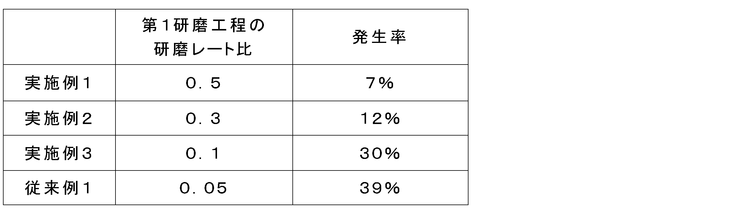
- Example 1 the step-like defect occurrence rate was 7%, and in Conventional Example 1, the step-like defect occurrence rate was 39%. Also in Examples 2 and 3, the number of silicon wafers in which the number of defects was 0 was confirmed in the same manner as in Example 1, and the occurrence rate of stepped defects was determined. The results are shown in Table 2 below. In Conventional Example 1, there is no distinction between the first polishing step and the second polishing step, and single-side polishing was performed at a constant SiO 2 / Si polishing rate ratio. However, Table 2 shows the polishing rate of the first polishing step.
Landscapes
- Engineering & Computer Science (AREA)
- Mechanical Engineering (AREA)
- Mechanical Treatment Of Semiconductor (AREA)
- Finish Polishing, Edge Sharpening, And Grinding By Specific Grinding Devices (AREA)
Abstract
Description
図1および図3を用いて、本発明の一実施形態に従うシリコンウェーハの片面研磨方法を説明する。本発明の一実施形態では、酸化シリコン膜20がベアなシリコン10の表面に形成されたシリコンウェーハWを研磨ヘッドにより把持し、研磨布が貼付された回転定盤にシリコンウェーハWを回転させながら押圧して、シリコンウェーハWの前記回転定盤側の片面を研磨する。
直径300mm、総厚み775μm(内、自然酸化膜の厚み:1nm)である同種のシリコンウェーハを複数用意し、スウェード素材の研磨布を定盤の表面に設置し、アルカリ研磨液を研磨スラリーとして供給しながら、バッチ式の片面研磨装置を用いて化学機械研磨による仕上げ研磨を行った。なお、研磨ヘッドおよび回転定盤の回転数は同一とし、同方向に回転させた。そして、回転定盤にシリコンウェーハを押圧する際の加圧力(g/cm2)ならびに、研磨ヘッドおよび回転定盤の回転数(rpm)のみを以下の条件で変化させた。すなわち、片面研磨装置100において、研磨ヘッドおよび回転定盤の回転数(rpm)を16,24,43,55とし、それぞれの回転数の下、加圧力(g/cm2)を50,60,100,150,200と変化させた。そして、研磨の取り代からSiO2研磨レートおよびSi研磨レート(nm/s)をそれぞれ求めた。このようにして求めたSiO2研磨レートおよびSi研磨レートから、SiO2/Si研磨レート比を求めた。結果を図7に示す。
予備実験例において用いたシリコンウェーハと同種のシリコンウェーハに対して、下記表1に示す研磨条件により第1研磨工程および第2研磨工程を行った。さらに、第2研磨工程後に、純水による研磨後のシリコンウェーハの洗浄工程を行った。その他の条件は予備実験例と同様にして、100枚のシリコンウェーハの片面研磨を行った。なお、表1中、SiO2/Si研磨レート比を単に「研磨レート比」と記載している。また、第1研磨工程におけるSiO2研磨レートは1nm/minであるため、60秒の研磨により酸化シリコン膜の全てが除去されたと考えてよい。また、第1研磨工程と第2研磨工程とでSiO2/Si研磨レート比は異なるが、第1研磨工程では低加圧且つ高速回転であり、第2研磨工程では高加圧且つ低速回転であるため、両研磨工程におけるSiO2研磨レートは同程度であった。

実施例1における第1研磨工程を行わず、研磨条件を表1に記載のとおりとした以外は、実施例1と同様にして、100枚のシリコンウェーハの片面研磨を行った。
実施例1における第1研磨工程の回転速度を変更してSiO2/Si研磨レート比を0.3とした以外は、実施例1と同様にして、100枚のシリコンウェーハの片面研磨を行った。
実施例1における第1研磨工程の回転速度を変更してSiO2/Si研磨レート比を0.1とした以外は、実施例1と同様にして、100枚のシリコンウェーハの片面研磨を行った。
実施例1および従来例1によるそれぞれのシリコンウェーハの研磨後の表面を、ウェーハ表面検査装置(Surfscan SP2; KLA-Tencor社製)を用いて、DICモード(DIC法による測定モード)により測定した。測定にあたって、凹凸形状の段差状微小欠陥の高さの閾値を3.4nmと設定し、この閾値を超える段差状微小欠陥の個数を求めた。こうして、DIC法により検出される欠陥個数が0個であったシリコンウェーハの枚数を、実施例1と従来例1とで確認した。実施例1では、100枚中93枚で段差状微小欠陥の発生が確認されず、一方、従来例1では、100枚中61枚で段差状微小欠陥の発生が確認されなかった。すなわち、実施例1では段差状欠陥の発生率は7%であり、従来例1では段差状欠陥の発生率は39%であった。実施例2,3についても、欠陥個数が0個であったシリコンウェーハの枚数を実施例1と同様に確認し、段差状欠陥の発生率を求めた。結果を下記の表2に示す。なお、従来例1では第1研磨工程と第2研磨工程の区別はなく一定のSiO2/Si研磨レート比で片面研磨を行ったが、表2中では第1研磨工程の研磨レートとして示す。
20 酸化シリコン膜
100 片面研磨装置
120 研磨ヘッド
130 研磨布
140 回転定盤
W 半導体ウェーハ(シリコンウェーハ)
Claims (4)
- 酸化シリコン膜がベアなシリコン表面に形成されたシリコンウェーハを研磨ヘッドにより把持し、研磨布が貼付された回転定盤に前記シリコンウェーハを回転させながら押圧して、前記シリコンウェーハの前記回転定盤側の片面を研磨するシリコンウェーハの片面研磨方法であって、
前記シリコンウェーハを押圧する加圧力ならびに前記シリコンウェーハおよび前記回転定盤の相対速度に関する第1研磨条件により、前記シリコンウェーハの前記片面の研磨を行う第1研磨工程と、
該第1研磨工程の後、前記第1研磨条件における前記加圧力および前記相対速度の少なくともいずれかを変化させた第2研磨条件により、前記シリコンウェーハの前記片面の研磨を行う第2研磨工程と、を含み、
前記第1研磨条件によるシリコン研磨レートに対する酸化シリコン研磨レートの研磨レート比が、前記第2研磨条件によるシリコン研磨レートに対する酸化シリコン研磨レートの研磨レート比よりも大きいことを特徴とするシリコンウェーハの片面研磨方法。 - 少なくとも前記酸化シリコン膜を除去するまで前記第1研磨工程を行う、請求項1に記載のシリコンウェーハの片面研磨方法。
- 前記第1研磨条件による前記研磨レート比が0.5以上である、請求項1または2に記載のシリコンウェーハの片面研磨方法。
- 前記第2研磨条件による前記研磨レート比が0.5未満である、請求項1~3のいずれか1項に記載のシリコンウェーハの片面研磨方法。
Priority Applications (4)
| Application Number | Priority Date | Filing Date | Title |
|---|---|---|---|
| CN201680081068.4A CN108885982B (zh) | 2016-02-03 | 2016-12-02 | 硅晶圆的单面抛光方法 |
| DE112016006354.7T DE112016006354B4 (de) | 2016-02-03 | 2016-12-02 | Siliziumwafer-einseiten-polierverfahren |
| US16/069,300 US11628534B2 (en) | 2016-02-03 | 2016-12-02 | Silicon wafer single-side polishing method |
| KR1020187016000A KR102102719B1 (ko) | 2016-02-03 | 2016-12-02 | 실리콘 웨이퍼의 편면 연마 방법 |
Applications Claiming Priority (2)
| Application Number | Priority Date | Filing Date | Title |
|---|---|---|---|
| JP2016018759A JP6418174B2 (ja) | 2016-02-03 | 2016-02-03 | シリコンウェーハの片面研磨方法 |
| JP2016-018759 | 2016-02-03 |
Publications (1)
| Publication Number | Publication Date |
|---|---|
| WO2017134919A1 true WO2017134919A1 (ja) | 2017-08-10 |
Family
ID=59499507
Family Applications (1)
| Application Number | Title | Priority Date | Filing Date |
|---|---|---|---|
| PCT/JP2016/085929 Ceased WO2017134919A1 (ja) | 2016-02-03 | 2016-12-02 | シリコンウェーハの片面研磨方法 |
Country Status (7)
| Country | Link |
|---|---|
| US (1) | US11628534B2 (ja) |
| JP (1) | JP6418174B2 (ja) |
| KR (1) | KR102102719B1 (ja) |
| CN (1) | CN108885982B (ja) |
| DE (1) | DE112016006354B4 (ja) |
| TW (1) | TWI619159B (ja) |
| WO (1) | WO2017134919A1 (ja) |
Families Citing this family (4)
| Publication number | Priority date | Publication date | Assignee | Title |
|---|---|---|---|---|
| JP7092092B2 (ja) * | 2019-05-09 | 2022-06-28 | 信越半導体株式会社 | 片面研磨方法 |
| CN111993265B (zh) * | 2020-08-28 | 2021-11-26 | 上海华力微电子有限公司 | 判断研磨头的胶膜是否扭曲的方法 |
| KR102929295B1 (ko) * | 2021-03-03 | 2026-02-24 | 어플라이드 머티어리얼스, 인코포레이티드 | Cmp에서 온도로 제어되는 제거 속도 |
| CN119609906A (zh) * | 2024-12-27 | 2025-03-14 | 西安奕斯伟材料科技股份有限公司 | 用于晶圆的最终抛光方法及抛光晶圆 |
Citations (2)
| Publication number | Priority date | Publication date | Assignee | Title |
|---|---|---|---|---|
| JPH10242090A (ja) * | 1997-02-28 | 1998-09-11 | Toshiba Corp | 半導体ウエハの研磨方法および研磨装置 |
| JP2011042536A (ja) * | 2009-08-21 | 2011-03-03 | Sumco Corp | エピタキシャルシリコンウェーハの製造方法 |
Family Cites Families (25)
| Publication number | Priority date | Publication date | Assignee | Title |
|---|---|---|---|---|
| JP2000315665A (ja) * | 1999-04-29 | 2000-11-14 | Ebara Corp | 研磨方法及び装置 |
| JP3916375B2 (ja) * | 2000-06-02 | 2007-05-16 | 株式会社荏原製作所 | ポリッシング方法および装置 |
| JP2002050595A (ja) * | 2000-08-04 | 2002-02-15 | Hitachi Ltd | 研磨方法、配線形成方法及び半導体装置の製造方法 |
| US6790768B2 (en) * | 2001-07-11 | 2004-09-14 | Applied Materials Inc. | Methods and apparatus for polishing substrates comprising conductive and dielectric materials with reduced topographical defects |
| JP2005203729A (ja) * | 2003-12-19 | 2005-07-28 | Ebara Corp | 基板研磨装置 |
| JP3917593B2 (ja) * | 2004-02-05 | 2007-05-23 | 株式会社東芝 | 半導体装置の製造方法 |
| JP2005277130A (ja) * | 2004-03-25 | 2005-10-06 | Fujitsu Ltd | 半導体装置の製造方法 |
| JP2008036783A (ja) * | 2006-08-08 | 2008-02-21 | Sony Corp | 研磨方法および研磨装置 |
| JP2008091594A (ja) | 2006-10-02 | 2008-04-17 | Sumitomo Electric Ind Ltd | 半導体ウエハの枚葉研磨装置 |
| JP4696086B2 (ja) * | 2007-02-20 | 2011-06-08 | 信越半導体株式会社 | シリコン単結晶ウエーハの仕上げ研磨方法及びシリコン単結晶ウエーハ |
| WO2009046296A1 (en) * | 2007-10-05 | 2009-04-09 | Saint-Gobain Ceramics & Plastics, Inc. | Polishing of sapphire with composite slurries |
| CN101417407B (zh) * | 2007-10-25 | 2011-10-05 | 中芯国际集成电路制造(上海)有限公司 | 化学机械研磨方法 |
| CN101456150B (zh) * | 2007-12-11 | 2011-09-28 | 上海华虹Nec电子有限公司 | 化学机械抛光方法 |
| CN101656195A (zh) * | 2008-08-22 | 2010-02-24 | 北京有色金属研究总院 | 大直径硅片的制造方法 |
| JP4990300B2 (ja) * | 2009-01-14 | 2012-08-01 | パナソニック株式会社 | 半導体装置の製造方法 |
| TWI498954B (zh) * | 2009-08-21 | 2015-09-01 | 勝高股份有限公司 | 磊晶矽晶圓的製造方法 |
| JP5649417B2 (ja) * | 2010-11-26 | 2015-01-07 | 株式会社荏原製作所 | 固定砥粒を有する研磨テープを用いた基板の研磨方法 |
| US8440094B1 (en) * | 2011-10-27 | 2013-05-14 | Rohm And Haas Electronic Materials Cmp Holdings, Inc. | Method of polishing a substrate |
| CN104416466A (zh) * | 2013-08-26 | 2015-03-18 | 中芯国际集成电路制造(上海)有限公司 | 一种用于化学机械抛光工艺的抛光垫修整方法 |
| CN103659468B (zh) * | 2013-12-09 | 2016-06-29 | 天津中环领先材料技术有限公司 | 一种减少单晶硅晶圆抛光片化学灼伤的有蜡抛光方法 |
| CN104802071A (zh) * | 2014-01-24 | 2015-07-29 | 中芯国际集成电路制造(上海)有限公司 | 化学机械抛光方法 |
| JP6244962B2 (ja) | 2014-02-17 | 2017-12-13 | 株式会社Sumco | 半導体ウェーハの製造方法 |
| WO2016006553A1 (ja) * | 2014-07-09 | 2016-01-14 | 日立化成株式会社 | Cmp用研磨液及び研磨方法 |
| JP6206360B2 (ja) | 2014-08-29 | 2017-10-04 | 株式会社Sumco | シリコンウェーハの研磨方法 |
| JP6421640B2 (ja) * | 2015-02-25 | 2018-11-14 | 株式会社Sumco | 半導体ウェーハの枚葉式片面研磨方法および半導体ウェーハの枚葉式片面研磨装置 |
-
2016
- 2016-02-03 JP JP2016018759A patent/JP6418174B2/ja active Active
- 2016-12-02 US US16/069,300 patent/US11628534B2/en active Active
- 2016-12-02 WO PCT/JP2016/085929 patent/WO2017134919A1/ja not_active Ceased
- 2016-12-02 DE DE112016006354.7T patent/DE112016006354B4/de active Active
- 2016-12-02 KR KR1020187016000A patent/KR102102719B1/ko active Active
- 2016-12-02 CN CN201680081068.4A patent/CN108885982B/zh active Active
- 2016-12-08 TW TW105140590A patent/TWI619159B/zh active
Patent Citations (2)
| Publication number | Priority date | Publication date | Assignee | Title |
|---|---|---|---|---|
| JPH10242090A (ja) * | 1997-02-28 | 1998-09-11 | Toshiba Corp | 半導体ウエハの研磨方法および研磨装置 |
| JP2011042536A (ja) * | 2009-08-21 | 2011-03-03 | Sumco Corp | エピタキシャルシリコンウェーハの製造方法 |
Also Published As
| Publication number | Publication date |
|---|---|
| JP2017139311A (ja) | 2017-08-10 |
| KR20180075668A (ko) | 2018-07-04 |
| TWI619159B (zh) | 2018-03-21 |
| DE112016006354T5 (de) | 2018-10-11 |
| CN108885982A (zh) | 2018-11-23 |
| CN108885982B (zh) | 2022-11-22 |
| US11628534B2 (en) | 2023-04-18 |
| JP6418174B2 (ja) | 2018-11-07 |
| KR102102719B1 (ko) | 2020-04-21 |
| DE112016006354B4 (de) | 2024-02-15 |
| TW201735145A (zh) | 2017-10-01 |
| US20190030676A1 (en) | 2019-01-31 |
Similar Documents
| Publication | Publication Date | Title |
|---|---|---|
| KR101002250B1 (ko) | 에피택셜 웨이퍼 제조 방법 | |
| TWI390616B (zh) | Semiconductor wafer manufacturing method | |
| KR101994782B1 (ko) | 경면연마 웨이퍼의 제조방법 | |
| CN103456321B (zh) | 磁记录介质用玻璃基板 | |
| JP4696086B2 (ja) | シリコン単結晶ウエーハの仕上げ研磨方法及びシリコン単結晶ウエーハ | |
| JP6418174B2 (ja) | シリコンウェーハの片面研磨方法 | |
| WO2011077661A1 (ja) | 半導体ウェーハおよびその製造方法 | |
| JP5472073B2 (ja) | 半導体ウェーハ及びその製造方法 | |
| JP3943869B2 (ja) | 半導体ウエーハの加工方法および半導体ウエーハ | |
| JP5598371B2 (ja) | ガラス基板の研磨方法 | |
| JP2015220370A (ja) | シリコンウェーハの製造方法及びシリコンウェーハ | |
| JP6323515B2 (ja) | 半導体ウェーハのラッピング方法および半導体ウェーハ | |
| JP6432497B2 (ja) | 研磨方法 | |
| WO2014185003A1 (ja) | ワークの研磨装置 | |
| JP6747376B2 (ja) | シリコンウエーハの研磨方法 | |
| KR101581469B1 (ko) | 웨이퍼 연마방법 | |
| JP4809033B2 (ja) | 拡散ウェーハの製造方法 | |
| TW200908120A (en) | Manufacturing method of semiconductor device | |
| TW202407790A (zh) | 晶圓的單面拋光方法、晶圓的製造方法、及晶圓的單面拋光裝置 | |
| CN117226680A (zh) | 衬底及其制造方法 | |
| JP2007149923A (ja) | 半導体ウェーハの平坦化加工方法 | |
| JP2002110594A (ja) | ウェーハの表面研磨方法 |
Legal Events
| Date | Code | Title | Description |
|---|---|---|---|
| 121 | Ep: the epo has been informed by wipo that ep was designated in this application |
Ref document number: 16889402 Country of ref document: EP Kind code of ref document: A1 |
|
| ENP | Entry into the national phase |
Ref document number: 20187016000 Country of ref document: KR Kind code of ref document: A |
|
| WWE | Wipo information: entry into national phase |
Ref document number: 112016006354 Country of ref document: DE |
|
| 122 | Ep: pct application non-entry in european phase |
Ref document number: 16889402 Country of ref document: EP Kind code of ref document: A1 |