WO2017133169A1 - 连接有负电容的多栅FinFET及其制造方法及电子设备 - Google Patents
连接有负电容的多栅FinFET及其制造方法及电子设备 Download PDFInfo
- Publication number
- WO2017133169A1 WO2017133169A1 PCT/CN2016/087249 CN2016087249W WO2017133169A1 WO 2017133169 A1 WO2017133169 A1 WO 2017133169A1 CN 2016087249 W CN2016087249 W CN 2016087249W WO 2017133169 A1 WO2017133169 A1 WO 2017133169A1
- Authority
- WO
- WIPO (PCT)
- Prior art keywords
- gate
- layer
- fin
- substrate
- finfet
- Prior art date
- Legal status (The legal status is an assumption and is not a legal conclusion. Google has not performed a legal analysis and makes no representation as to the accuracy of the status listed.)
- Ceased
Links
Images




Classifications
-
- H—ELECTRICITY
- H10—SEMICONDUCTOR DEVICES; ELECTRIC SOLID-STATE DEVICES NOT OTHERWISE PROVIDED FOR
- H10D—INORGANIC ELECTRIC SEMICONDUCTOR DEVICES
- H10D30/00—Field-effect transistors [FET]
- H10D30/60—Insulated-gate field-effect transistors [IGFET]
- H10D30/62—Fin field-effect transistors [FinFET]
-
- H—ELECTRICITY
- H10—SEMICONDUCTOR DEVICES; ELECTRIC SOLID-STATE DEVICES NOT OTHERWISE PROVIDED FOR
- H10D—INORGANIC ELECTRIC SEMICONDUCTOR DEVICES
- H10D30/00—Field-effect transistors [FET]
- H10D30/01—Manufacture or treatment
- H10D30/021—Manufacture or treatment of FETs having insulated gates [IGFET]
- H10D30/023—Manufacture or treatment of FETs having insulated gates [IGFET] having multiple independently-addressable gate electrodes influencing the same channel
-
- H—ELECTRICITY
- H10—SEMICONDUCTOR DEVICES; ELECTRIC SOLID-STATE DEVICES NOT OTHERWISE PROVIDED FOR
- H10D—INORGANIC ELECTRIC SEMICONDUCTOR DEVICES
- H10D30/00—Field-effect transistors [FET]
- H10D30/01—Manufacture or treatment
- H10D30/021—Manufacture or treatment of FETs having insulated gates [IGFET]
- H10D30/024—Manufacture or treatment of FETs having insulated gates [IGFET] of fin field-effect transistors [FinFET]
-
- H—ELECTRICITY
- H10—SEMICONDUCTOR DEVICES; ELECTRIC SOLID-STATE DEVICES NOT OTHERWISE PROVIDED FOR
- H10D—INORGANIC ELECTRIC SEMICONDUCTOR DEVICES
- H10D30/00—Field-effect transistors [FET]
- H10D30/60—Insulated-gate field-effect transistors [IGFET]
- H10D30/611—Insulated-gate field-effect transistors [IGFET] having multiple independently-addressable gate electrodes influencing the same channel
-
- H—ELECTRICITY
- H10—SEMICONDUCTOR DEVICES; ELECTRIC SOLID-STATE DEVICES NOT OTHERWISE PROVIDED FOR
- H10D—INORGANIC ELECTRIC SEMICONDUCTOR DEVICES
- H10D30/00—Field-effect transistors [FET]
- H10D30/60—Insulated-gate field-effect transistors [IGFET]
- H10D30/62—Fin field-effect transistors [FinFET]
- H10D30/6215—Fin field-effect transistors [FinFET] having multiple independently-addressable gate electrodes
-
- H—ELECTRICITY
- H10—SEMICONDUCTOR DEVICES; ELECTRIC SOLID-STATE DEVICES NOT OTHERWISE PROVIDED FOR
- H10D—INORGANIC ELECTRIC SEMICONDUCTOR DEVICES
- H10D64/00—Electrodes of devices having potential barriers
- H10D64/01—Manufacture or treatment
- H10D64/017—Manufacture or treatment using dummy gates in processes wherein at least parts of the final gates are self-aligned to the dummy gates, i.e. replacement gate processes
-
- H—ELECTRICITY
- H10—SEMICONDUCTOR DEVICES; ELECTRIC SOLID-STATE DEVICES NOT OTHERWISE PROVIDED FOR
- H10D—INORGANIC ELECTRIC SEMICONDUCTOR DEVICES
- H10D84/00—Integrated devices formed in or on semiconductor substrates that comprise only semiconducting layers, e.g. on Si wafers or on GaAs-on-Si wafers
- H10D84/01—Manufacture or treatment
- H10D84/0123—Integrating together multiple components covered by H10D12/00 or H10D30/00, e.g. integrating multiple IGBTs
- H10D84/0126—Integrating together multiple components covered by H10D12/00 or H10D30/00, e.g. integrating multiple IGBTs the components including insulated gates, e.g. IGFETs
- H10D84/0158—Integrating together multiple components covered by H10D12/00 or H10D30/00, e.g. integrating multiple IGBTs the components including insulated gates, e.g. IGFETs the components including FinFETs
-
- H—ELECTRICITY
- H10—SEMICONDUCTOR DEVICES; ELECTRIC SOLID-STATE DEVICES NOT OTHERWISE PROVIDED FOR
- H10D—INORGANIC ELECTRIC SEMICONDUCTOR DEVICES
- H10D84/00—Integrated devices formed in or on semiconductor substrates that comprise only semiconducting layers, e.g. on Si wafers or on GaAs-on-Si wafers
- H10D84/01—Manufacture or treatment
- H10D84/02—Manufacture or treatment characterised by using material-based technologies
- H10D84/03—Manufacture or treatment characterised by using material-based technologies using Group IV technology, e.g. silicon technology or silicon-carbide [SiC] technology
- H10D84/038—Manufacture or treatment characterised by using material-based technologies using Group IV technology, e.g. silicon technology or silicon-carbide [SiC] technology using silicon technology, e.g. SiGe
-
- H—ELECTRICITY
- H10—SEMICONDUCTOR DEVICES; ELECTRIC SOLID-STATE DEVICES NOT OTHERWISE PROVIDED FOR
- H10D—INORGANIC ELECTRIC SEMICONDUCTOR DEVICES
- H10D84/00—Integrated devices formed in or on semiconductor substrates that comprise only semiconducting layers, e.g. on Si wafers or on GaAs-on-Si wafers
- H10D84/80—Integrated devices formed in or on semiconductor substrates that comprise only semiconducting layers, e.g. on Si wafers or on GaAs-on-Si wafers characterised by the integration of at least one component covered by groups H10D12/00 or H10D30/00, e.g. integration of IGFETs
- H10D84/82—Integrated devices formed in or on semiconductor substrates that comprise only semiconducting layers, e.g. on Si wafers or on GaAs-on-Si wafers characterised by the integration of at least one component covered by groups H10D12/00 or H10D30/00, e.g. integration of IGFETs of only field-effect components
- H10D84/83—Integrated devices formed in or on semiconductor substrates that comprise only semiconducting layers, e.g. on Si wafers or on GaAs-on-Si wafers characterised by the integration of at least one component covered by groups H10D12/00 or H10D30/00, e.g. integration of IGFETs of only field-effect components of only insulated-gate FETs [IGFET]
- H10D84/834—Integrated devices formed in or on semiconductor substrates that comprise only semiconducting layers, e.g. on Si wafers or on GaAs-on-Si wafers characterised by the integration of at least one component covered by groups H10D12/00 or H10D30/00, e.g. integration of IGFETs of only field-effect components of only insulated-gate FETs [IGFET] comprising FinFETs
-
- H—ELECTRICITY
- H10—SEMICONDUCTOR DEVICES; ELECTRIC SOLID-STATE DEVICES NOT OTHERWISE PROVIDED FOR
- H10D—INORGANIC ELECTRIC SEMICONDUCTOR DEVICES
- H10D86/00—Integrated devices formed in or on insulating or conducting substrates, e.g. formed in silicon-on-insulator [SOI] substrates or on stainless steel or glass substrates
- H10D86/01—Manufacture or treatment
- H10D86/011—Manufacture or treatment comprising FinFETs
-
- H—ELECTRICITY
- H10—SEMICONDUCTOR DEVICES; ELECTRIC SOLID-STATE DEVICES NOT OTHERWISE PROVIDED FOR
- H10D—INORGANIC ELECTRIC SEMICONDUCTOR DEVICES
- H10D86/00—Integrated devices formed in or on insulating or conducting substrates, e.g. formed in silicon-on-insulator [SOI] substrates or on stainless steel or glass substrates
- H10D86/201—Integrated devices formed in or on insulating or conducting substrates, e.g. formed in silicon-on-insulator [SOI] substrates or on stainless steel or glass substrates the substrates comprising an insulating layer on a semiconductor body, e.g. SOI
- H10D86/215—Integrated devices formed in or on insulating or conducting substrates, e.g. formed in silicon-on-insulator [SOI] substrates or on stainless steel or glass substrates the substrates comprising an insulating layer on a semiconductor body, e.g. SOI comprising FinFETs
-
- H—ELECTRICITY
- H10—SEMICONDUCTOR DEVICES; ELECTRIC SOLID-STATE DEVICES NOT OTHERWISE PROVIDED FOR
- H10D—INORGANIC ELECTRIC SEMICONDUCTOR DEVICES
- H10D62/00—Semiconductor bodies, or regions thereof, of devices having potential barriers
- H10D62/10—Shapes, relative sizes or dispositions of the regions of the semiconductor bodies; Shapes of the semiconductor bodies
- H10D62/17—Semiconductor regions connected to electrodes not carrying current to be rectified, amplified or switched, e.g. channel regions
- H10D62/351—Substrate regions of field-effect devices
- H10D62/357—Substrate regions of field-effect devices of FETs
- H10D62/364—Substrate regions of field-effect devices of FETs of IGFETs
- H10D62/371—Inactive supplementary semiconductor regions, e.g. for preventing punch-through, improving capacity effect or leakage current
Definitions
- the present disclosure relates to semiconductor technology, and more particularly to a multi-gate fin field effect transistor (FinFET) and a method of fabricating the same, and an electronic device including the same, wherein one of the gates of the multi-gate FinFET is connected to a negative capacitance.
- FinFET fin field effect transistor
- Sub-threshold Swing is an important performance parameter of metal oxide semiconductor field effect transistors (MOSFETs), which is greater than zero, and it is desirable that the smaller the better.
- MOSFETs metal oxide semiconductor field effect transistors
- the limit value of SS at room temperature is about 60 mV/dec, and it is difficult to reduce as the device size shrinks. It is expected to achieve smaller SS to improve device performance.
- An object of the present disclosure is at least in part to provide a fin field effect transistor (FinFET) having a plurality of gates and one of which is connected with a negative capacitance, a method of fabricating the same, and an electronic device including the same.
- FinFET fin field effect transistor
- a FinFET comprising: a fin extending in a first direction on a substrate; a first side of the fin on the substrate extending in a second direction intersecting the first direction to form a fin An intersecting first gate; a second gate on the substrate opposite the first side of the fin extending in the second direction to intersect the fin and opposite the first gate; and formed in the metallization stack and A negative capacitor connected to the second gate.
- an electronic device that includes an integrated circuit formed by the FinFET described above.
- a method of fabricating a FinFET comprising: forming a fin extending in a first direction on a substrate; forming a first side and a second side of the fin on the substrate, respectively a first gate extending in a second direction intersecting and intersecting the fin and a second gate opposite the first gate; and a negative capacitor connected to the second gate in the metallization stack.
- a separate first gate and a second gate may be formed for a FinFET (eg, a bulk FinFET or a SOI FinFET), and a negative capacitor may be connected to the second gate.
- a negative capacitor With such a negative capacitor, the total capacitance at the second gate can be made negative, so that the subthreshold swing (SS) can be effectively reduced.
- the first gate may not be connected to the negative capacitor. The turn-off current can be effectively reduced by the first gate.
- FIG. 1 is a schematic circuit diagram showing a fin field effect transistor (FinFET) according to an embodiment of the present disclosure
- FIGS. 2(a)-2(q) are cross-sectional views showing partial stages in a process of fabricating a FinFET in accordance with an embodiment of the present disclosure
- 3(a)-3(m) are cross-sectional views showing a partial stage in a process of fabricating a FinFET in accordance with another embodiment of the present disclosure.
- a layer/element when referred to as being "on" another layer/element, the layer/element may be directly on the other layer/element, or there may be a central layer between them/ element. In addition, if a layer/element is "on” another layer/element, the layer/element may be "under” the other layer/element when the orientation is reversed.
- FIG. 1 is a schematic circuit diagram showing a fin field effect transistor (FinFET) according to an embodiment of the present disclosure.
- FinFET fin field effect transistor
- the FinFET 100 includes a first gate (G1), a second gate (G2), a source (S), and a drain (D).
- the FinFET 100 is formed in a multi-gate structure, for example, the first gate G1 may be a control gate, and the second gate G2 may be a back gate, and vice versa.
- the FinFET 100 may include fins extending in a first direction on a substrate, and the first gate G1 and the second gate G2 may extend in a second direction intersecting the first direction to intersect the fins.
- the first gate and the second gate are opposite each other and each may affect a channel region formed in the fin.
- the source region S and the drain region D may be formed on both sides of the channel region, for example, formed at an end of the fin or formed in another semiconductor layer epitaxially grown on the end of the fin.
- the first gate and the second gate may be substantially aligned in the second direction and spaced apart from each other (eg, through a fin between and optionally also through a dielectric layer at the top of the fin).
- the first gate G1 and the second gate G2 may have substantially the same stacked configuration.
- each of the first gate G1 and the second gate G2 may include a stack of gate dielectric and gate electrode layers (eg, a high K/metal gate stack).
- a work function adjusting layer may be interposed between the gate dielectric and the gate electrode layer.
- the first gate G1 (especially due to the gate dielectric layer therein) will result in a first gate capacitance, here denoted by C g ; likewise, the second gate (especially due to the gate dielectric therein) The layer) will result in a second gate capacitance 1031, denoted here by C.
- This first gate capacitance C g and the second gate capacitance C are inherent capacitances of the device.
- the negative capacitor 1033 may be connected in series on the second gate G2. Therefore, the negative capacitor 1033 appears in series with the second gate capacitor 1031.
- the capacitor includes a plate-dielectric layer-plate configuration in which the dielectric layer can store charge.
- Conventional capacitors have a "positive" capacitance characteristic, that is, as the charge stored in the dielectric layer increases, the voltage between the two plates increases.
- such a dielectric layer is referred to as a conventional dielectric layer, or simply referred to as a dielectric layer, which is the same as the term is conventional in the art.
- certain materials can exhibit a "negative" capacitance characteristic under certain conditions, that is, as the charge stored therein increases, the voltage between the plates appears to decrease.
- This material is called a “negative capacitance material.”
- some ferroelectric materials such as materials containing Zr, Ba or Sr, such as HfZrO 2 , BaTiO 3 , KH 2 PO 4 or NBT or any combination thereof
- Polarization causes a large amount of bound charge to accumulate instantaneously on the surface of the material, causing the voltage across the ferroelectric material to decrease.
- C is the capacitance value of the second gate capacitance 1031
- C n is the capacitance value of the negative capacitor 1033 (as described above, is a negative value)
- represents the absolute value of C n .
- the subthreshold swing (SS) may be expressed as:
- the SS may be expressed as:
- the negative capacitor may be formed in the form of a trench capacitor.
- the trench capacitor can increase the opposing plate area of the capacitor and thus increase the capacitance value.
- a trench may be formed in one or more layers of the metallization stack and a negative capacitor may be formed in the trench (eg, by forming a first conductive layer - a negative capacitive material layer - a second conductive layer in the trench) Laminated).
- Capacitance The layers in the stack configuration may extend along the sidewalls and bottom walls of the trench.
- Each of the conductive layers may include various suitable conductive materials such as metals, metal nitrides, and the like, or a stacked configuration thereof.
- the conductive material may include materials used to form conductive contacts in a semiconductor process, such as conductive diffusion barrier materials such as TiN and metal electrode materials such as W.
- the metal electrode material can form a low ohmic contact and is suitable for a conductive layer that requires a connection with other components.
- a conductive diffusion barrier material layer may be used in combination therewith.
- Such a FinFET can be fabricated as follows. For example, fins extending in a first direction may be formed on the substrate.
- the substrate may be a bulk semiconductor substrate or a semiconductor-on-insulator (SOI) substrate.
- a first side of the fin on the substrate may form a first gate extending in a second direction intersecting the first direction to intersect the fin, and a second side opposite the first side of the fin on the substrate is formed along the first side
- a second gate extending in two directions to intersect the fin and opposite the first gate.
- first gate and the second gate have substantially the same stacked configuration, they can be fabricated in the same process.
- a stack for the gate can be formed on the fin-formed substrate (including the first side and the second side of the fin), and then the stack is divided into two on the first side and the second side of the fin Part (for example, this can be achieved simply by etch back the stack).
- the already separated stack can then be patterned into the final grid shape.
- the same mask extending in the second direction and across the fins may be utilized, such that substantial self-alignment of the first gate and the second gate in the second direction may be achieved.
- the present disclosure is not limited to, for example, the first gate and the second gate may also have different stacked configurations.
- the first side and the second side of the fin can be processed separately.
- the desired stack of the first gate can be formed on the first side and the desired stack of the second gate can be formed on the second side and patterned to form the final gate shape.
- a replacement gate process can be utilized.
- a sacrificial gate extending in a second direction to intersect the fin may be formed on the substrate.
- the sacrificial gate can include a first portion on a first side of the fin and a second portion on a second side of the fin.
- the first portion of the sacrificial gate can be removed (eg, by selective etching) to form a first gate in the space left by the removal of the first portion; and the sacrificial gate can be removed (eg, by selective etching)
- the second portion forms a second grid in the space left by the removal of the second portion.
- the first gate and the second gate are substantially identical
- the first portion and the second portion of the sacrificial gate may be formed of the same layer of sacrificial material, and their removal may be simultaneously performed by the same etching recipe, filling the space left by their removal.
- the first gate and the second gate can also be simultaneously performed.
- a negative capacitor connected in series can be formed.
- a negative capacitor can be formed in the metallization stack (eg, in the form of a trench capacitor) and can be connected to the second gate by a metallization interconnect.
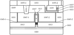
- FIGS. 2(a)-2(q) are cross-sectional views showing partial stages in a process of fabricating a FinFET in accordance with an embodiment of the present disclosure.
- a substrate 1001 is provided.
- a silicon wafer will be described as an example to illustrate the case of a bulk FinFET.
- the present disclosure is not limited thereto, but can be applied to other various forms of substrates.
- a well region 1003 may be formed.
- a well region can be formed by ion implantation and annealing. If an n-type device is to be formed, a p-type well region can be formed; or, if a p-type device is to be formed, an n-type well region can be formed.
- an n-type well region may be formed by implanting an n-type ion such as P or As or the like into the substrate 1001, and a p-type ion such as BF2 or In or the like may be implanted to form a p-type well region.
- well region 1003 is located inside substrate 1001.
- fins extending in the first direction may be formed by patterning the substrate 1001.
- fins may be formed by a pattern transfer technique.
- the amorphous silicon layer 1007 may be formed on the substrate 1001 by, for example, deposition such as chemical vapor deposition (CVD), atomic layer deposition (ALD), or the like.
- an etch stop layer 1005 may be formed on the surface of the substrate 1001 by, for example, deposition, before forming these material layers.
- the etch stop layer 1005 may include an oxide (eg, silicon oxide) having a thickness of about 1 to 5 nm; and the amorphous silicon layer 1007 may have a thickness of about 50 to 150 nm.
- a photoresist PR1 patterned by, for example, photolithography (exposure, development) can be formed on the amorphous silicon layer 1007, and then the photoresist PR1 is used as a mask to
- the crystalline silicon layer 1007 is patterned such as reactive ion etching (RIE).
- RIE reactive ion etching
- the RIE can stop at the etch stop layer 1005.
- the photoresist PR1 can be removed.
- the patterned amorphous silicon layer 1007 may have a side extending in the first direction The wall, the position of the side wall corresponds to a side wall of the fin to be formed later.
- a spacer 1011 may be formed on the sidewall of the patterned amorphous silicon layer 1007.
- the spacer 1011 may include nitride, and the width (the dimension in the horizontal direction in the drawing) is about 5 to 30 nm.
- Such a sidewall may, for example, be deposited by depositing a layer of nitride in a substantially conformal manner, and then RIE the deposited nitride layer in a direction substantially perpendicular to the surface of the substrate to remove lateral extensions thereof leaving Its vertical extension is formed.
- the area occupied by the side wall 1011 corresponds to the area where the fin is to be formed.
- the amorphous silicon layer 1007 can be removed by selective etching such as RIE.
- RIE selective etching
- a spacer 1011 extending in a first direction is obtained which can serve as a hard mask for forming the fins.
- the side wall 1011 can be further patterned as RIE to define its length in the first direction.
- the substrate 1001 may be patterned by using the sidewall 1011 as a mask to form fins.
- the etch barrier layer 1005 and the substrate 1001 may be selectively etched by, for example, RIE.
- etching of the substrate 1001 can proceed into the well region 1003.
- the surface of the remaining portion of the substrate is recessed, thereby forming a protruding fin F on the substrate 1001.
- the manner of forming the fin is not limited to this.
- the fin may be formed by forming a photoresist corresponding to the shape of the fin to be formed on the substrate 1001 and patterning the substrate 1001 using a photoresist such as RIE.
- a gate intersecting the fin may be formed on the fin-formed substrate.
- an alternative gate process is taken as an example.
- an isolation layer may be formed first for the isolation gate and the substrate.
- the oxide layer 1013 can be formed on the substrate by, for example, deposition such as CVD, and the oxide layer is subjected to a planarization treatment such as chemical mechanical polishing (CMP). The planarization process can be stopped at the side wall 1011.
- CMP chemical mechanical polishing
- the oxide layer 1013 may be etched back (for example, by wet etching such as diluting HF acid or by HF vapor) to form an isolation layer.
- the top surface of the isolation layer 1013 is lower than the top surface of the fin F, and preferably not lower than the surface of the well region 1003.
- a punch-through prevention (PTS) layer can also be formed to improve device performance.
- PTS punch-through prevention
- ion implantation can be performed substantially perpendicular to the direction of the surface of the substrate.
- p-type ions can be implanted; and for the p-type device to be formed, n can be implanted Type ions.
- the energy of the ion implantation can be controlled such that it does not substantially penetrate the layers above the substrate 1001 and directly reaches the substrate 1001.
- the isolation layer 1013 due to the scattering of the implanted ions by the isolation layer 1013, a portion of the scattered ions may enter the substrate 1001 as indicated by the oblique arrows in the figure. Annealing may be performed to activate ions such that these scattered ions may form doped regions 1015 in substrate 1001, as shown in Figure 2(g), which may then serve as a PTS. Since the doped region 1015 is due to scattering of the isolation layer 1013, its top surface may be substantially flush with the top surface of the isolation layer 1013 (or slightly higher due to upward scattering and/or diffusion factors).
- a sacrificial material layer 1019 may be formed on the isolation layer 1013.
- polysilicon can be formed by deposition, and the deposited polysilicon layer can be planarized, such as CMP, and CMP can be stopped at the sidewall spacers 1011; then, the polysilicon layer is etched back to form the sacrificial material layer 1019.
- the top surface of the sacrificial material layer 1019 is preferably higher than the top surface of the fin F.
- the top surface of the first sacrificial material layer 1019 is preferably lower than the top surface of the spacer 1011, which helps to separate the first gate and the second gate. That is, the top surface of the sacrificial material layer 1019 may be located between the top surface and the bottom surface of the side wall 1011.
- the interface layer 1017 may be formed on the sidewall of the fin F before the sacrificial material layer 1019 is formed.
- the interfacial layer 1017 can include an oxide having a thickness of about 1-3 nm. In this example, since both are oxides, interface layer 1017 and etch stop layer 1005 are then shown integrally as 1017.
- the sacrificial material layer 1019 can then be patterned to form a sacrificial gate.
- a photoresist PR2 may be formed on the sacrificial material layer 1019.
- the photoresist PR2 can be formed into a shape corresponding to a sacrificial gate to be formed by photolithography (for example, exposure, development, etc.). Specifically, as shown in FIGS.
- the photoresist PR2 may be patterned in a direction intersecting (for example, perpendicular) with the fin F (defined by the sidewall 1011) (horizontal direction in the figure) ) extended strips. Then, as shown in FIG. 2(j), the patterned photoresist layer PR2 is used as a mask, and the sacrificial material layer 1019 is selectively etched such as RIE. Thus, the sacrificial material layer 1019 constitutes a sacrificial gate, such as the patterned photoresist PR2, which has a strip shape extending in a direction intersecting (for example, perpendicular) to the fin F.
- a gate spacer can be formed on the sidewall of the sacrificial gate for source/drain implantation (or by external Extending the semiconductor layer to form strain source/drain) and the like. FinFET fabrication using a replacement gate process is well known to those skilled in the art and will not be described herein.
- the sacrificial gate can then be removed to form the final gate structure, including the first gate and the second gate.
- a further dielectric layer 1031 (eg, an oxide) may be formed on the isolation layer 1013.
- the oxide layer may be deposited on the structure shown in FIG. 2(j) and then planarized, such as CMP, to form the dielectric layer 1031.
- the CMP can stop at the sacrificial material layer 1019, exposing the sacrificial material layer 1019 for subsequent replacement.
- the top surface of the sacrificial material layer 1019 is higher than the top surface of the fin F, a part of the side wall 1011 after the CMP remains on the top of the fin F.
- the fin F and its top side wall 1011 divide the sacrificial material layer 1019 into two portions on the first side (eg, the left side in the figure) and the second side (eg, the right side in the figure) of the fin F.
- the sacrificial material layer 1019 can be removed by selective etching (for example, using a TMAH solution).
- a gate trench (not shown, which is originally occupied by the sacrificial material layer 1019) is left on the first side and the second side (right side in the figure) of the fin F.
- a stack of materials for the gate can then be filled in the gate trench.
- the gate dielectric layers 1045-1/1045-2 and the first gate electrode layers 1047-1/1047-2 may be sequentially formed.
- the gate dielectric layer may include a high-k gate dielectric such as HfO 2 having a thickness of about 1 to 5 nm; and the gate electrode layer may include a conductive metal such as W.
- the gate dielectric layer can be deposited in a substantially conformal manner, and the gate electrode layer can be deposited to fill the gate trench, and then planarized, such as CMP (which can be used as the stop point of the sidewall 1011), to the gate trench. Fill these layers in.
- the interface layer can be reconstructed prior to forming the gate dielectric layer.
- a gate work function adjusting layer (not shown) may be formed between the gate dielectric layer and the gate electrode layer.
- a first gate (1045-1, 1047-1) is formed on the first side of the fin F, respectively, and a second gate (1045-2, 1047-2) is formed on the second side of the fin F.
- one of the first gate and the second gate can be used as a control gate and the other can be used as a back gate.
- a metallization stack can be formed.
- an interlayer dielectric layer 1049 (for example, an oxide) may be formed on the structure shown in FIG. 2(1), for example, by deposition.
- a contact portion 1051-1 may be formed.
- the contact portion may be formed, for example, by etching an interlayer dielectric layer to form a contact hole, and filling the contact hole with a conductive material layer (for example, W).
- a contact portion may be formed at a position corresponding to a source/drain region (not shown).
- a (conductive) diffusion barrier layer such as TiN is then filled with a conductive material.
- a negative capacitor can be formed.
- a photoresist PR3 may be formed on the interlayer dielectric layer 1049 on which the contact portion is formed.
- the photoresist PR3 can be patterned by photolithography to expose a portion of the interlayer dielectric layer 1049, after which a negative capacitor will be formed.
- the capacitance of the subsequently formed negative capacitor can be adjusted by adjusting the size of the exposed portion of the photoresist PR3.
- the patterned photoresist layer PR3 is used as a mask, and the interlayer dielectric layer 1049 is selectively etched, such as RIE, until the second gate (specifically, the gate electrode layer 1047-2 thereof) is exposed, thereby inter-layer dielectric.
- a trench R1 is formed in the layer 1049.
- the contact hole R1 is preferably biased to the side opposite to the first grid (the right side in the drawing). Thereafter, the photoresist PR3 can be removed.
- the first conductive layer may include a TiN layer 1033 (eg, having a thickness of about 1-5 nm, which may be formed by ALD).
- the TiN layer 1033 acts as a plate of the negative capacitor on the one hand due to its electrical conductivity and can also be used as a diffusion barrier on the one hand.
- the first conductive layer may also include one or more layers of ohmic contact layers such as metals (e.g., W, etc.) of low ohmic resistance, if desired (e.g., to reduce contact resistance).
- the negative capacitance material layer may include a HfZrO 2 layer 1035 (for example, having a thickness of about 2 to 100 nm, which may be formed by ALD).
- the second conductive layer may include a TiN layer 1037 (eg, having a thickness of about 1-5 nm, which may be formed by ALD) and an ohmic contact layer 1039 (eg, a metal such as W, which may be formed by ALD or CVD), acting as a capacitor. Another plate.
- the TiN layer 1037 is mainly used as a diffusion barrier layer (which may be omitted), and the ohmic contact layer 1039 may be in contact with other contact members that are subsequently formed (for example, see 1055-2 shown in FIG. 2(q)).
- the TiN layer 1033, the HfZrO 2 layer 1035, and the TiN layer 1037 may be sequentially deposited in a substantially conformal manner, and the ohmic contact layer 1039 may be deposited to fill the trench R1, and then planarized, for example, CMP, to These layers are filled in the trench R1.
- one plate (1033) of the negative capacitor (1033, 1035, 1037, 1039) directly contacts the gate electrode layer 1047-2 and is thus connected to the second gate.
- a metal interconnection (see FIG. 2(q)) is formed in the upper layer of the interlayer dielectric layer 1049, it may be as shown in FIG. 2(p), and may be selectively etched, for example. RIE, the TiN layer 1033, the HfZrO 2 layer 1035, and the TiN layer 1037 are etched back so that they are recessed. Subsequently, as shown in FIG. 2(q), another interlayer dielectric layer 1053 (for example, an oxide) is formed on the interlayer dielectric layer 1049.
- an oxide is formed on the interlayer dielectric layer 1049.
- metal interconnections 1055-1 and 1055-2 corresponding to the contact portion 1051-1 and the ohmic contact layer 1039 may be formed.
- the metal interconnects 1055-1 and 1055-2 may extend in a manner in the interlayer dielectric layer 1053 to electrically connect the contact portion 1051-1 and the ohmic contact layer 1039 (the other plate of the negative capacitor) to other components. Since the TiN layer 1033, the HfZrO 2 layer 1035, and the TiN layer 1037 are recessed and recessed by the interlayer dielectric layer 1053, unnecessary electrical connections between them and the metal interconnect 1055-2 can be avoided.
- the trench R1 is biased to one side of the second gate (the right side in the drawing).
- the trench R1 may also be located directly above the second gate (the width of the trench R1 is smaller than the width of the second gate).
- a conductive via may be formed in the interlayer dielectric layer 1053 (a metal interconnection may be formed in a further layer), and the conductive via may be aligned with the contact portion 1051-1 and the gate electrode layer 1047-2, and the like, respectively. In this case, it is not necessary to recess the TiN layer 1033, the HfZrO 2 layer 1035, and the TiN layer 1037 as described above.
- a negative capacitor can also be formed on the upper layer of the metallization stack and connected to the second gate through conductive vias and/or metal interconnects.
- 3(a)-3(m) are cross-sectional views showing a partial stage in a process of fabricating a FinFET in accordance with another embodiment of the present disclosure.
- the SOI substrate 2001 may include a base substrate 2001-1 (eg, silicon), a buried insulating layer 2001-2 (eg, an oxide), and an SOI layer 2001-3 (eg, silicon).
- a base substrate 2001-1 eg, silicon
- a buried insulating layer 2001-2 eg, an oxide
- an SOI layer 2001-3 eg, silicon
- an etch barrier layer 2005 and an amorphous silicon layer 2007 may be sequentially formed.
- the etch barrier layer 2005 and the amorphous silicon layer 2007, reference may be made to the above description of the etch barrier layer 1005 and the amorphous silicon layer 1007.
- the amorphous silicon layer 2007 may be patterned such as RIE using a patterned photoresist PR4 to form sidewalls extending in a first direction, the positions of the sidewalls corresponding to the subsequent formation One side wall of the fin.
- the RIE can stop at the etch stop layer 2005.
- a hard mask for defining the fins can then be formed.
- the spacers 2011 may be formed on the sidewalls of the patterned amorphous silicon layer 2007.
- FIG. 2(c) reference can be made to the description above in connection with FIG. 2(c).
- the sidewall spacers 2011 may be used as a mask to sequentially selectively etch the barrier layer 2005 (if any) and the substrate 2001 (specifically, the SOI layer 2001-3).
- the etch is like RIE to form the fins.
- the etching of the substrate 2001 may stop at the buried insulating layer 2001-2.
- the surface of the remaining portion of the substrate is recessed, thereby forming a protruding fin F on the substrate 2001.
- a gate intersecting the fin F may be formed on the fin-formed substrate. Since this example relates to an SOI substrate, it is not necessary to separately form an isolation layer.
- a sacrificial material layer 2019 may be formed on the buried insulating layer 2001-2.
- the interface layer 2017 may be formed on the sidewall of the fin F before the formation of the sacrificial material layer 2019.
- the sacrificial material layer 2019 can then be patterned to form a sacrificial gate.
- a photoresist PR5 may be formed on the sacrificial material layer 2019.
- the photoresist PR5 can be formed into a shape corresponding to a sacrificial gate to be formed by photolithography (for example, exposure, development, etc.). For this, for example, reference can be made to the above description in conjunction with FIGS. 2(i) and 2(i'). Then, as shown in FIG.
- the patterned photoresist layer PR5 is used as a mask, and the sacrificial material layer 2019 is selectively etched such as RIE.
- the RIE may stop at the buried insulating layer 2001-2.
- the sacrificial material layer 2019 constitutes a sacrificial gate that is strip-shaped extending in a direction intersecting (eg, perpendicular) to the fin F.
- the fin F and the sacrificial gate are formed as described above, fabrication of other portions of the device can be performed. Thereafter, the sacrificial gate can be removed to form a final gate structure including the first gate and the second gate.
- a further dielectric layer 2031 (eg, an oxide) may be formed on the buried insulating layer 2001-2. Then, the sacrificial material layer 2019 is removed, and the first gate and the second gate are filled in spaces left on both sides of the fin F due to their removal, respectively.
- the first gate may include a gate dielectric layer 2045-1 and a gate electrode layer 2047-1
- the second gate may include a gate dielectric layer 2045-2 and a gate electrode layer 2047-2.
- the stacked configuration of the first gate and the second gate may be substantially the same. For this, for example, reference can be made to the description above in connection with FIGS. 2(k) and 2(1).
- fabrication of the metallization stack can be performed and a negative capacitor can be formed therein.
- an interlayer dielectric layer 2049 (for example, an oxide) may be formed on the structure shown in FIG. 3(i), for example, by deposition. At a position corresponding to the first gate, a contact portion 2051-1 may be formed. Further, as shown in FIG. 3(k), the trench R2 may be formed in the interlayer dielectric layer 1049 by using the patterned photoresist PR6. A negative capacitor can be formed by filling the trench R2 with various material layers. For example, as shown in FIG. 3(1), a stacked configuration of the first conductive layer-negative capacitance material layer-second conductive layer may be sequentially formed in the trench R1. In the example of FIG.
- the first conductive layer may include a TiN layer 2033 (eg, having a thickness of about 1-5 nm), and the negative capacitive material layer may include a HfZrO 2 layer 2035 (eg, having a thickness of about 2 to 100 nm)
- the second conductive layer may include a TiN layer 2037 (eg, having a thickness of about 1-5 nm) and an ohmic contact layer 2039 (eg, a metal such as W).
- metal interconnections 2055-1 and 2055-2 may also be formed in another interlayer dielectric layer 2049 as shown in FIG. 3(m).
- a semiconductor device can be applied to various electronic devices. For example, by integrating a plurality of such semiconductor devices and other devices (eg, other forms of transistors, etc.), an integrated circuit (IC) can be formed, and thereby an electronic device can be constructed. Accordingly, the present disclosure also provides an electronic device including the above semiconductor device.
- the electronic device can also include a display screen that mates with the integrated circuit and a wireless transceiver that mates with the integrated circuit.
- Such electronic devices are, for example, smart phones, tablet computers (PCs), personal digital assistants (PDAs), and the like.
- a method of fabricating a chip system is also provided.
- the method can include the above method of fabricating a semiconductor device.
- a variety of devices can be integrated on a chip, at least some of which are fabricated in accordance with the methods of the present disclosure.
Landscapes
- Insulated Gate Type Field-Effect Transistor (AREA)
- Metal-Oxide And Bipolar Metal-Oxide Semiconductor Integrated Circuits (AREA)
- Semiconductor Integrated Circuits (AREA)
- Thin Film Transistor (AREA)
Abstract
一种多栅FinFET及其制造方法及包括该FinFET的电子设备,其中多栅FinFET的栅极之一与负电容连接。FinFET可以包括:在衬底上沿第一方向延伸的鳍;在衬底上鳍的第一侧沿与第一方向相交的第二方向延伸从而与鳍相交的第一栅;在衬底上与第一侧相对的第二侧沿第二方向延伸从而与鳍相交且与第一栅相对的第二栅;以及在金属化叠层中形成且连接到第二栅的负电容器。
Description
相关申请的引用
本申请要求于2016年2月5日递交的题为“连接有负电容的多栅FinFET及其制造方法及电子设备”的中国专利申请201610082481.4的优先权,其内容一并于此用作参考。
本公开涉及半导体技术,更具体地,涉及一种多栅鳍式场效应晶体管(FinFET)及其制造方法及包括该FinFET的电子设备,其中该多栅FinFET的栅极之一与负电容连接。
亚阈值摆幅(Sub-threshold Swing,SS)是金属氧化物半导体场效应晶体管(MOSFET)的一项重要性能参数,其大于零,且希望其越小越好。目前,在室温条件下SS的极限值约为60mV/dec,且难以随着器件尺寸的缩小而降低。期望能够实现更小的SS,以改善器件性能。
发明内容
本公开的目的至少部分地在于提供一种具有多个栅极且其中一个栅极连接有负电容的鳍式场效应晶体管(FinFET)及其制造方法以及包括该FinFET的电子设备。
根据本公开的一个方面,提供了一种FinFET,包括:在衬底上沿第一方向延伸的鳍;在衬底上鳍的第一侧沿与第一方向相交的第二方向延伸从而与鳍相交的第一栅;在衬底上鳍的与第一侧相对的第二侧沿第二方向延伸从而与鳍相交且与第一栅相对的第二栅;以及在金属化叠层中形成且连接到第二栅的负电容器。
根据本公开的另一方面,提供了一种电子设备,包括上述FinFET形成的集成电路。
根据本公开的再一方面,提供了一种制造FinFET的方法,包括:在衬底上形成沿第一方向延伸的鳍;在衬底上鳍的第一侧和第二侧分别形成沿与第一方向相交的第二方向延伸且与鳍相交的第一栅以及与第一栅相对的第二栅;以及在金属化叠层中形成与第二栅连接的负电容器。
根据本公开的实施例,可以对FinFET(例如,体FinFET或SOI FinFET)形成分离的第一栅和第二栅,在第二栅上可以连接有负电容器。通过这种负电容器,可以使得在第二栅处总的电容为负值,从而可以有效降低亚阈值摆幅(SS)。另一方面,第一栅可以不连接负电容器。通过第一栅,可以有效降低关断电流。
通过以下参照附图对本公开实施例的描述,本公开的上述以及其他目的、特征和优点将更为清楚,在附图中:
图1是示出了根据本公开实施例的鳍式场效应晶体管(FinFET)的示意电路图;
图2(a)-2(q)是示出了根据本公开实施例的制造FinFET的流程中部分阶段的截面图;
图3(a)-3(m)是示出了根据本公开另一实施例的制造FinFET的流程中部分阶段的截面图。
以下,将参照附图来描述本公开的实施例。但是应该理解,这些描述只是示例性的,而并非要限制本公开的范围。此外,在以下说明中,省略了对公知结构和技术的描述,以避免不必要地混淆本公开的概念。
在附图中示出了根据本公开实施例的各种结构示意图。这些图并非按比例绘制,其中为了清楚表达的目的,放大了某些细节,并且可能省略了某些细节。图中所示出的各种区域、层的形状以及它们之间的相对大小、位置关系仅是示例性的,实际中可能由于制造公差或技术限制而有所偏差,并且本领域技术人员根据实际所需可以另外设计具有不同形状、大小、相对位置的区域/层。
在本公开的上下文中,当将一层/元件称作位于另一层/元件“上”时,该层/元件可以直接位于该另一层/元件上,或者它们之间可以存在居中层/元件。另外,如果在一种朝向中一层/元件位于另一层/元件“上”,那么当调转朝向时,该层/元件可以位于该另一层/元件“下”。
图1是示出了根据本公开实施例的鳍式场效应晶体管(FinFET)的示意电路图。
如图1所示,根据该实施例的FinFET 100包括第一栅(G1)、第二栅(G2)、源极(S)和漏极(D)。在此,FinFET 100形成为多栅结构,例如第一栅G1可以是控制栅,第二栅G2可以是背栅,反之亦然。根据本公开的实施例,FinFET100可以包括在衬底上沿第一方向延伸的鳍,第一栅G1和第二栅G2可以沿与第一方向相交的第二方向延伸,以便与鳍相交。第一栅和第二栅彼此相对,且均可以影响鳍中形成的沟道区。源区S和漏区D可以形成在沟道区两侧,例如形成于鳍的端部或者形成于在鳍的端部上外延的另外半导体层中。在此,第一栅和第二栅可以在第二方向上实质上对准,且彼此分隔开(例如,通过之间的鳍以及可选地还通过鳍顶部的电介质层)。
根据本公开的实施例,第一栅G1和第二栅G2可以具有实质上相同的叠层配置。例如,第一栅G1和第二栅G2各自均可以包括栅介质和栅电极层的叠层(例如,高K/金属栅叠层)。根据实施例,栅介质和栅电极层之间可以插入功函数调节层。
如本领域技术人员所知,第一栅G1(特别是由于其中的栅介质层)将导致第一栅电容,在此以Cg来表示;同样,第二栅(特别是由于其中的栅介质层)将导致第二栅电容1031,在此以C来表示。这种第一栅电容Cg和第二栅电容C是器件固有的电容。
根据本公开的实施例,可以在第二栅G2上串联连接负电容器1033。因此,负电容器1033表现为与第二栅电容1031相串联。一般地,电容器包括极板-电介质层-极板的配置,电介质层可以储存电荷。常规的电容器呈“正”电容特性,即,当电介质层储存的电荷增多时,两个极板间的电压增大。在本公开中,将这种电介质层称作常规电介质层,或者直接简称为电介质层,这与该术语在本领域的常规含义相同。与此不同,某些材料在一定状态下,可以呈现“负”
电容特性,即,随着其中储存的电荷增多,极板间的电压反而表现为降低。这种材料称作“负电容材料”。例如,某些铁电材料(例如含Zr、Ba或Sr的材料,如HfZrO2、BaTiO3、KH2PO4或NBT或其任意组合等)在到达某一临界电场时,可发生极化现象。极化使得大量的束缚电荷瞬间积累在材料的表面,使铁电材料两端的电压减小。
由于串联关系,第二栅G2处的总电容Ct可以表示为:
Ct=|Cn|C/(|Cn|-C),
其中,C是第二栅电容1031的电容值,Cn是负电容器1033的电容值(如上所述,为负值),|Cn|表示Cn的绝对值。
如果第一栅G1是控制栅(此时,第二栅G2可以是背栅),则亚阈值摆幅(SS)可以表示为:
SS≈60(1+Ct/Cg)mV/dec。
根据上式可以看出,当Ct<0时,可以实现小于60mV/dec的SS。因此,优选地,|Cn|<C。另外,当SS大于零且数值越小时,器件性能越佳。因此,优选地|Ct|近似等于(或者说,略小于)Cg。此时(1/Ct+1/Cg)小于零,故第一栅G1与第二栅G2之间的总电容小于零,此时晶体管是不稳定的,也即具有电滞性。
备选地,如果第二栅G2是控制栅(此时,第一栅G1可以是背栅),则SS可以表示为:
SS≈60(1+Cg/Ct)mV/dec。
根据上式可以看出,当Ct<0时,也可以实现小于60mV/dec的SS。因此,优选地,|Cn|<C。同理,当SS大于零且数值越小时,器件性能越佳。因此,优选地|Ct|近似等于(或者说,略大于)Cg。此时(1/Ct+1/Cg)大于零,故第一栅G1与第二栅G2之间的总电容大于零,此时晶体管是稳定的,没有电滞性,是通常晶体管优先的工作状态。
根据本公开的实施例,负电容器可以形成为沟槽电容器的形式。在有限的面积中,沟槽电容器可以增大电容器相对的极板面积,并因此增大电容值。例如,可以金属化叠层的一层或多层中形成沟槽,并在沟槽中形成负电容器(例如,通过在沟槽中形成第一导电层-负电容材料层-第二导电层的叠层)。电容
器叠层配置中的层可以沿着沟槽的侧壁和底壁延伸。
各导电层(第一导电层、第二导电层等)可以包括各种合适的导电材料,例如金属、金属氮化物等,或它们的叠层配置。为了更好地与半导体工艺相兼容,导电材料可以包括半导体工艺中用来形成导电接触的材料,例如导电性的扩散阻挡材料如TiN以及金属电极材料如W等。金属电极材料可以形成低欧姆接触,从而适于需要与其他部件形成连接的导电层。另外,为了避免金属电极材料的扩散,可以与之配合使用导电性扩散阻挡材料层。
这种FinFET可以如下来制造。例如,可以在衬底上形成沿第一方向延伸的鳍。衬底可以是体(bulk)半导体衬底或者绝缘体上半导体(SOI)衬底。在衬底上鳍的第一侧可以形成沿与第一方向相交的第二方向延伸以便与鳍相交的第一栅,且在衬底上鳍的与第一侧相对的第二侧形成沿第二方向延伸以便与鳍相交且与第一栅相对的第二栅。
在第一栅和第二栅具有实质上相同叠层配置的情况下,它们可以在相同的处理中来制作。例如,可以在形成有鳍的衬底上(包括鳍的第一侧和第二侧)形成用于栅的叠层,然后将该叠层分成分处于鳍的第一侧和第二侧的两部分(例如,这可以简单地通过回蚀该叠层来实现)。然后,可以将已经分开的叠层构图为最终的栅形状。在构图时,可以利用沿第二方向延伸且跨过鳍的相同掩模,这样可以实现第一栅和第二栅在第二方向上实质上的自对准。
当然,本公开不限于,例如第一栅和第二栅也可以具有不同的叠层配置。这种情况下,可以对鳍的第一侧和第二侧分别进行处理。例如,可以在第一侧形成第一栅所需的叠层,而在第二侧形成第二栅所需的叠层,并对它们进行构图来形成最终的栅形状。本领域存在多种方式来在衬底上的不同区域形成不同材料。
根据实施例,可以利用替代栅工艺。具体地,可以在衬底上形成沿第二方向延伸以便与鳍相交的牺牲栅。该牺牲栅可以包括位于鳍的第一侧的第一部分以及位于鳍的第二侧的第二部分。可以(例如,通过选择性刻蚀)去除牺牲栅的第一部分,以在由于该第一部分的去除而留下的空间中形成第一栅;并可以(例如,通过选择性刻蚀)去除牺牲栅的第二部分,以在由于该第二部分的去除而留下的空间中形成第二栅。如上所述,在第一栅和第二栅具有实质上相同
叠层配置的情况下,牺牲栅的第一部分和第二部分可以由相同的牺牲材料层形成,它们的去除可以通过相同的刻蚀配方同时完成,向由于它们的去除而留下的空间中填入第一栅和第二栅也可以同时进行。
对于第二栅,可以形成与之串联连接的负电容器。例如,负电容器可以形成于金属化叠层中(例如,形成为沟槽电容器的形式),并可以通过金属化互连而连接到第二栅。
本公开的技术可以各种方式来呈现,以下将描述其中一些示例。
图2(a)-2(q)是示出了根据本公开实施例的制造FinFET的流程中部分阶段的截面图。
如图2(a)所示,提供衬底1001。在此,以硅晶片为例进行描述,以便说明体FinFET的情况。但是,本公开不限于此,而是可以适用于其他各种形式的衬底。
在衬底1001中,可以形成阱区1003。例如,可以通过离子注入,并进行退火来形成这种阱区。如果要形成n型器件,则可以形成p型阱区;或者,如果要形成p型器件,则可以形成n型阱区。例如,可以通过向衬底1001中注入n型离子如P或As等来形成n型阱区,注入p型离子如BF2或In等来形成p型阱区。在该示例中,阱区1003位于衬底1001内部。
在形成有阱区1003的衬底1001上,可以通过对衬底1001进行构图来形成沿第一方向(在该示例中,垂直于纸面的方向)延伸的鳍。
根据本公开的实施例,可以通过图形转移技术来形成鳍。具体地,可以在衬底1001上,可以通过例如淀积如化学气相淀积(CVD)、原子层淀积(ALD)等,形成非晶硅层1007。另外,在形成这些材料层之前,可以通过例如淀积,在衬底1001的表面上形成刻蚀阻挡层1005。例如,刻蚀阻挡层1005可以包括氧化物(例如,氧化硅),厚度为约1~5nm;非晶硅层1007的厚度可以为约50~150nm。
然后,如图2(b)所示,可以在非晶硅层1007上形成例如通过光刻(曝光、显影)构图的光刻胶PR1,然后再以该光刻胶PR1为掩模,对非晶硅层1007进行构图如反应离子刻蚀(RIE)。RIE可以停止于刻蚀阻挡层1005。之后,可以去除光刻胶PR1。构图后的非晶硅层1007可以具有沿第一方向延伸的侧
壁,该侧壁的位置对应于随后将要形成的鳍的一个侧壁。
接着,如图2(c)所示,可以在构图后的非晶硅层1007的侧壁上形成侧墙(spacer)1011。例如,侧墙1011可以包括氮化物,宽度(图中水平方向的维度)为约5~30nm。这种侧墙例如可以通过以大致共形的方式淀积一层氮化物层,然后以大致垂直于衬底表面的方向对淀积的氮化物层进行RIE,以去除其横向延伸部分而留下其竖直延伸部分来形成。侧墙1011所占区域对应于将要形成鳍的区域。之后,可以通过选择性刻蚀如RIE,去除非晶硅层1007。这样,得到了沿第一方向延伸的侧墙1011,该侧墙可以充当用来形成鳍的硬掩模。当然,还可以对侧墙1011进一步构图如RIE,以限定其沿第一方向的长度。
随后,如图2(d)所示,可以侧墙1011为掩模,对衬底1001进行构图,来形成鳍。具体地,可以通过例如RIE,依次对刻蚀阻挡层1005和衬底1001进行选择性刻蚀。优选地,对衬底1001的刻蚀可以进行到阱区1003中。
这样,相对于侧墙1011下方的部分,衬底其余部分的表面下凹,从而在衬底1001上形成突出的鳍F。
当然,形成鳍的方式不限于此。例如,可以通过在衬底1001上形成与将要形成的鳍的形状相对应的光刻胶,并利用光刻胶对衬底1001进行构图如RIE来形成鳍。
接着,可以在形成有鳍的衬底上形成与鳍相交的栅。在以下的描述中,以替代栅工艺为例。
在本示例(即,硅晶片)中,为隔离栅和衬底,可以先形成隔离层。具体地,如图2(e)所示,可以通过例如淀积如CVD,在衬底上形成氧化物层1013,并对该氧化物层进行平坦化处理如化学机械抛光(CMP)。平坦化处理可以停止于侧墙1011。接着,如图2(f)所示,可以对氧化物层1013进行回蚀(例如,通过湿法腐蚀如稀释HF酸,或者通过HF蒸气),以形成隔离层。隔离层1013的顶面低于鳍F的顶面,且优选地不低于阱区1003的表面。
此外,为改善器件性能,还可以形成穿通阻止(PTS)层。例如,如图2(f)中的箭头所示,可以大致垂直于衬底表面的方向,进行离子注入。对于将要形成的n型器件,可以注入p型离子;而对于将要形成的p型器件,可以注入n
型离子。可以控制离子注入的能量,使得其基本上不能穿透衬底1001上方的各层而直接到达衬底1001中。但是,由于隔离层1013对注入离子的散射,可以有一部分被散射的离子进入衬底1001中,如图中的倾斜箭头所示。可以进行退火激活离子,从而这些散射离子可以在衬底1001中形成掺杂区1015,如图2(g)所示,该掺杂区随后可以充当PTS。由于该掺杂区1015是由于隔离层1013的散射导致的,因此其顶面可以与隔离层1013的顶面大致齐平(或者由于向上的散射和/或扩散因素而略高)。
接着,如图2(h)所示,可以在隔离层1013上形成牺牲材料层1019。例如,可以通过淀积形成多晶硅,并对淀积的多晶硅层进行平坦化处理如CMP,CMP可以停止于侧墙1011;然后,对多晶硅层进行回蚀,来形成牺牲材料层1019。在此,牺牲材料层1019的顶面优选地高于鳍F的顶面。这样,随后在替代栅工艺中可以确保有一部分侧墙1011可以留于鳍的顶部。另外,还可以确保随后形成的第一栅和第二栅可以与鳍的侧壁的整个高度相接。另一方面,第一牺牲材料层1019的顶面优选地低于侧墙1011的顶面,这有助于分离第一栅和第二栅。即,牺牲材料层1019的顶面可以位于侧墙1011的顶面和底面之间。另外,在形成牺牲材料层1019之前,可以在鳍F的侧壁上形成界面层1017。例如,界面层1017可以包括氧化物,厚度为约1~3nm。在该示例中由于均为氧化物,之后将界面层1017和刻蚀阻挡层1005一体示出为1017。
然后,可以对牺牲材料层1019进行构图,以形成牺牲栅。例如,如图2(i)的俯视图和2(i′)的截面图(沿图2(i)中AA′线的截面图)所示,可以在牺牲材料层1019上形成光刻胶PR2,该光刻胶PR2可以通过光刻(例如,曝光、显影等)而形成与将要形成的牺牲栅相对应的形状。具体地,如图2(i)和2(i′)所示,可以将光刻胶PR2构图为沿与鳍F(由侧墙1011限定)相交(例如,垂直)的方向(图中水平方向)延伸的条状。然后,如图2(j)所示,可以构图后的光刻胶PR2为掩模,对牺牲材料层1019进行选择性刻蚀如RIE。这样,牺牲材料层1019构成牺牲栅,该牺牲栅如构图后的光刻胶PR2呈沿着与鳍F相交(例如,垂直)的方向延伸的条状。
在如上所述形成鳍F和牺牲栅1019之后,可以进行器件其他部分的制造。例如,可以在牺牲栅的侧壁上形成栅侧墙,可以进行源/漏注入(或者通过外
延半导体层来形成应变源/漏)等等。本领域技术人员熟知利用替代栅工艺的FinFET制造,在此不再赘述。
然后,可以去除牺牲栅,以形成最终的栅结构,包括第一栅和第二栅。
具体地,如图2(k)所示,可以在隔离层1013上形成进一步的电介质层1031(例如,氧化物)。例如,可以在图2(j)所示的结构上淀积氧化物,然后对其进行平坦化处理如CMP,来形成电介质层1031。CMP可以停止于牺牲材料层1019,从而露出牺牲材料层1019,以便随后将它们置换。如上所述,由于牺牲材料层1019的顶面高于鳍F的顶面,因此CMP之后一部分侧墙1011留于鳍F的顶部。鳍F及其顶部的侧墙1011将牺牲材料层1019分为位于鳍F第一侧(例如,图中左侧)和第二侧(例如,图中右侧)的两部分。
接着,如图2(1)所示,可以通过选择性刻蚀(例如,利用TMAH溶液),去除牺牲材料层1019。这样,在鳍F的第一侧和第二侧(图中右侧)留下了栅槽(未示出,为牺牲材料层1019原本所占据的空间)。然后,可以在栅槽中填充用于栅的材料叠层。例如,可以依次形成栅介质层1045-1/1045-2和第一栅电极层1047-1/1047-2。例如,栅介质层可以包括高K栅介质如HfO2,厚度为约1~5nm;栅电极层可以包括导电金属如W。例如,可以通过依次以大致共形的方式淀积栅介质层,并淀积栅电极层以填满栅槽,然后进行平坦化处理如CMP(可以侧墙1011为停止点),来向栅槽中填充这些层。在形成栅介质层之前,可以先重构界面层。另外,在栅介质层和栅电极层之间,还可以形成栅功函数调节层(未示出)。
这样,分别在鳍F的第一侧形成了第一栅(1045-1、1047-1),在鳍F的第二侧形成了第二栅(1045-2、1047-2)。例如,第一栅和第二栅之一可以用作控制栅,另一个可以用作背栅。
接着,可以形成金属化叠层。
例如,如图2(m)所示,可以在图2(1)所示的结构上例如通过淀积形成层间电介质层1049(例如,氧化物)。在与第一栅相对应的位置处,可以形成接触部1051-1。接触部例如可以通过刻蚀层间电介质层形成接触孔,并在接触孔中填充导电材料层(例如,W)来形成。同样地,可以在与源/漏区(未示出)相对应的位置处,形成接触部。当然,也可以先在接触孔的侧壁和底壁上先形
成(导电性)扩散阻挡层如TiN,然后再填充导电材料。
在层间电介质层1049中,可以形成负电容器。
例如,如图2(n)所示,可以在形成有接触部的层间电介质层1049上形成光刻胶PR3。可以通过光刻,将该光刻胶PR3构图为露出层间电介质层1049的一部分,此后将在该部分中形成负电容器。可以通过调节光刻胶PR3所露出部分的大小,来调节随后形成的负电容器的电容。然后,可以构图的光刻胶PR3为掩模,对层间电介质层1049进行选择性刻蚀如RIE,直至露出第二栅(具体地,其栅电极层1047-2),从而在层间电介质层1049中形成沟槽R1。在此,接触孔R1优选地偏向与第一栅相反的一侧(图中右侧)。之后,可以去除光刻胶PR3。
随后,可以向沟槽R1中填充各种材料层,来形成负电容器。例如,如图2(o)所示,可以依次在沟槽R1中形成第一导电层-负电容材料层-第二导电层的叠层配置。在图2(o)的示例中,第一导电层可以包括TiN层1033(例如,厚度为约1-5nm,可以通过ALD来形成)。该TiN层1033一方面由于其导电性而充当负电容器的一个极板,一方面也可以用作扩散阻挡层。如果需要的话(例如,为了降低接触点电阻),第一导电层还可以包括低欧姆电阻的一层或多层欧姆接触层如金属(例如,W等)。负电容材料层可以包括HfZrO2层1035(例如,厚度为约2~100nm,可以通过ALD来形成)。第二导电层可以包括TiN层1037(例如,厚度为约约1-5nm,可以通过ALD来形成)和欧姆接触层1039(例如,金属如W,可以通过ALD或CVD来形成),充当电容器的另一个极板。在此,TiN层1037主要用作扩散阻挡层(可以省略),欧姆接触层1039可以与随后形成的其他接触部件(例如,参见图2(q)所示的1055-2)接触。例如,可以通过依次以大致共形的方式淀积TiN层1033、HfZrO2层1035和TiN层1037,并淀积欧姆接触层1039以填满沟槽R1,然后进行平坦化处理例如CMP,来向沟槽R1中填充这些层。
在该示例中,负电容器(1033、1035、1037、1039)的一个极板(1033)直接接触栅电极层1047-2,并因此连接到第二栅。
接着,还可以形成金属化叠层中的其他层。在该示例中,由于在层间电介质层1049的上一层中形成金属互连(参见图2(q))的形式,可以先如图2(p)
所示,可以通过选择性刻蚀如RIE,对TiN层1033、HfZrO2层1035和TiN层1037进行回蚀,使得它们下凹。随后,如图2(q)所示,在层间电介质层1049上形成另一层间电介质层1053(例如,氧化物)。在该层间电介质层1053中,可以形成于接触部1051-1以及欧姆接触层1039相对应的金属互连1055-1和1055-2。金属互连1055-1和1055-2可以在层间电介质层1053中按一定路线延伸,从而将接触部1051-1以及欧姆接触层1039(负电容器的另一个极板)电连接到其他部件。由于TiN层1033、HfZrO2层1035和TiN层1037下凹且下凹处被层间电介质层1053填充,可以避免它们与金属互连1055-2之间不必要的电连接。
在以上示例中,沟槽R1偏向第二栅的一侧(图中右侧)。当然,本公开不限于此。例如,沟槽R1也可以位于第二栅正上方(沟槽R1的宽度小于第二栅的宽度)。另外,在层间电介质层1053中可以形成导电通道(via)(可以在再上一层中形成金属互连),导电通道可以分别对准接触部1051-1和栅电极层1047-2等。这种情况下,没有必要如上所述使TiN层1033、HfZrO2层1035和TiN层1037下凹。此外,负电容器也可以形成于金属化叠层中的更上层,并通过导电通道和/或金属互连而连接到第二栅。
图3(a)-3(m)是示出了根据本公开另一实施例的制造FinFET的流程中部分阶段的截面图。
如图3(a)所示,提供衬底2001。在此,以SOI衬底为例进行描述,以便说明SOI FinFET的情况。具体地,SOI衬底2001可以包括基底衬底2001-1(例如,硅)、埋入绝缘层2001-2(例如,氧化物)和SOI层2001-3(例如,硅)。
在衬底2001上,可以依次形成刻蚀阻挡层2005和非晶硅层2007。对于刻蚀阻挡层2005和非晶硅层2007,可以参见以上对刻蚀阻挡层1005和非晶硅层1007的描述。
如图3(b)所示,可以利用构图的光刻胶PR4,对非晶硅层2007进行构图如RIE以形成沿第一方向延伸的侧壁,该侧壁的位置对应于随后将要形成的鳍的一个侧壁。RIE可以停止于刻蚀阻挡层2005。对此,可以参见以上结合图2(b)的描述。
然后,可以形成用于限定鳍的硬掩模。例如,如图3(c)所示,可以在构图后的非晶硅层2007的侧壁上形成侧墙2011。对此,可以参见以上结合图2(c)的描述。
随后,如图3(d)所示,可以侧墙2011为掩模,依次对刻蚀阻挡层2005(如果有的话)以及衬底2001(具体地,SOI层2001-3)进行选择性刻蚀如RIE,来形成鳍。在此,对衬底2001的刻蚀可以停止于埋入绝缘层2001-2。
这样,相对于侧墙2011下方的部分,衬底其余部分的表面下凹,从而在衬底2001上形成突出的鳍F。接着,可以在形成有鳍的衬底上形成与鳍F相交的栅。由于该示例涉及SOI衬底,因此无需单独形成隔离层。
如图3(e)所示,可以在埋入绝缘层2001-2上形成牺牲材料层2019。另外,在形成牺牲材料层2019之前,可以在鳍F的侧壁上形成界面层2017。对此,例如可以参见以上结合图2(h)的描述。
然后,可以对牺牲材料层2019进行构图,以形成牺牲栅。
为此,如图3(f)的俯视图和3(f′)的截面图(沿图3(f)中AA′线的截面图)所示,可以在牺牲材料层2019上形成光刻胶PR5,该光刻胶PR5可以通过光刻(例如,曝光、显影等)而形成与将要形成的牺牲栅相对应的形状。对此,例如可以参见以上结合图2(i)和2(i′)的描述。然后,如图3(g)所示,可以构图后的光刻胶PR5为掩模,对牺牲材料层2019进行选择性刻蚀如RIE。RIE可以停止于埋入绝缘层2001-2。这样,牺牲材料层2019构成牺牲栅,该牺牲栅呈沿着与鳍F相交(例如,垂直)的方向延伸的条状。
在如上所述形成鳍F和牺牲栅之后,可以进行器件其他部分的制造。之后,可以去除牺牲栅,以形成最终的栅结构,包括第一栅和第二栅。
具体地,如图3(h)所示,可以在埋入绝缘层2001-2上形成进一步的电介质层2031(例如,氧化物)。然后,去除牺牲材料层2019,并分别向由于其去除而在鳍F两侧留下的空间中填充第一栅和第二栅。如图3(i)所示,第一栅可以包括栅介质层2045-1和栅电极层2047-1,第二栅可以包括栅介质层2045-2和栅电极层2047-2。第一栅和第二栅的叠层配置可以实质上相同。对此,例如可以参见以上结合图2(k)和2(1)的描述。
接着,可以进行金属化叠层的制作,并可以在其中形成负电容器。
例如,如图3(j)所示,可以在图3(i)所示的结构上例如通过淀积形成层间电介质层2049(例如,氧化物)。在与第一栅相对应的位置处,可以形成接触部2051-1。另外,如图3(k)所示,可以利用构图的光刻胶PR6,在层间电介质层1049中形成沟槽R2。可以通过向沟槽R2中填充各种材料层,来形成负电容器。例如,如图3(l)所示,可以依次在沟槽R1中形成第一导电层-负电容材料层-第二导电层的叠层配置。在图3(l)的示例中,第一导电层可以包括TiN层2033(例如,厚度为约约1-5nm),负电容材料层可以包括HfZrO2层2035(例如,厚度为约2~100nm),第二导电层可以包括TiN层2037(例如,厚度为约约1-5nm)和欧姆接触层2039(例如,金属如W)。之后,还可以在另一层间电介质层2049中形成金属互连2055-1和2055-2,如图3(m)所示。对此,例如可以参见以上结合图2(m)-2(q)的描述。
根据本公开实施例的半导体器件可以应用于各种电子设备。例如,通过集成多个这样的半导体器件以及其他器件(例如,其他形式的晶体管等),可以形成集成电路(IC),并由此构建电子设备。因此,本公开还提供了一种包括上述半导体器件的电子设备。电子设备还可以包括与集成电路配合的显示屏幕以及与集成电路配合的无线收发器等部件。这种电子设备例如智能电话、平板电脑(PC)、个人数字助手(PDA)等。
根据本公开的实施例,还提供了一种芯片系统(SoC)的制造方法。该方法可以包括上述制造半导体器件的方法。具体地,可以在芯片上集成多种器件,其中至少一些是根据本公开的方法制造的。
在以上的描述中,对于各层的构图、刻蚀等技术细节并没有做出详细的说明。但是本领域技术人员应当理解,可以通过各种技术手段,来形成所需形状的层、区域等。另外,为了形成同一结构,本领域技术人员还可以设计出与以上描述的方法并不完全相同的方法。另外,尽管在以上分别描述了各实施例,但是这并不意味着各个实施例中的措施不能有利地结合使用。
以上对本公开的实施例进行了描述。但是,这些实施例仅仅是为了说明的目的,而并非为了限制本公开的范围。本公开的范围由所附权利要求及其等价物限定。不脱离本公开的范围,本领域技术人员可以做出多种替代和修改,这些替代和修改都应落在本公开的范围之内。
Claims (26)
- 一种鳍式场效应晶体管(FinFET),包括:在衬底上沿第一方向延伸的鳍;在衬底上鳍的第一侧沿与第一方向相交的第二方向延伸从而与鳍相交的第一栅;在衬底上鳍的与第一侧相对的第二侧沿第二方向延伸从而与鳍相交且与第一栅相对的第二栅;以及在金属化叠层中形成且连接到第二栅的负电容器。
- 根据权利要求1所述的FinFET,其中,负电容器形成为金属化叠层中所包括的层间电介质层中的沟槽电容器。
- 根据权利要求1或2所述的FinFET,其中,负电容器的电容绝对值小于第二栅所导致的第二栅电容。
- 根据权利要求3所述的FinFET,其中,负电容器与第二栅电容的串联电容的绝对值近似等于第一栅所导致的第一栅电容。
- 根据权利要求3所述的FinFET,其中,负电容器的电容绝对值是第二栅电容的约1/2。
- 根据权利要求1或2所述的FinFET,还包括:位于鳍顶部的电介质层,其中第一栅和第二栅通过鳍及其顶部的电介质层而彼此分开。
- 根据权利要求1或2所述的FinFET,其中,第一栅和第二栅具有实质上相同的叠层配置。
- 根据权利要求1或2所述的FinFET,其中,负电容器包括第一导电层-负电容材料层-第二导电层的叠层。
- 根据权利要求8所述的FinFET,其中,第一导电层与第二栅相接触。
- 根据权利要求8所述的FinFET,其中,第一导电层和第二导电层中至少之一包括TiN。
- 根据权利要求8所述的FinFET,其中,第一导电层和第二导电层中至少之一包括导电材料的叠层。
- 根据权利要求8所述的FinFET,其中,负电容材料层包括铁电材料。
- 根据权利要求12所述的FinFET,其中,负电容材料层包括含Zr、Ba或Sr的材料。
- 根据权利要求13所述的FinFET,其中,负电容材料层包括HfZrO2、BaTiO3、KH2PO4或NBT或其任意组合。
- 根据权利要求1或2所述的FinFET,其中,衬底是体半导体衬底,且该FinFET还包括在位于鳍下方的衬底部分中形成的穿通阻止层。
- 根据权利要求1或2所述的FinFET,其中,衬底是绝缘体上半导体(SOI)衬底,且鳍形成于该SOI衬底的SOI层中。
- 一种电子设备,包括由如权利要求1-16中任一项所述的FinFET形成的集成电路。
- 根据权利要求17所述的电子设备,还包括:与所述集成电路配合的显示器以及与所述集成电路配合的无线收发器。
- 一种制造鳍式场效应晶体管(FinFET)的方法,包括:在衬底上形成沿第一方向延伸的鳍;在衬底上鳍的第一侧和第二侧分别形成沿与第一方向相交的第二方向延伸且与鳍相交的第一栅以及与第一栅相对的第二栅;以及在金属化叠层中形成与第二栅连接的负电容器。
- 根据权利要求19所述的方法,其中,形成第一栅以及形成第二栅包括:在衬底上形成沿第二方向延伸以便与鳍相交的牺牲栅,该牺牲栅包括位于鳍的第一侧的第一部分以及位于鳍的第二侧的第二部分;以及去除牺牲栅的第一部分和第二部分,并在由于第一部分和第二部分的去除而留下的空间中分别形成第一栅和第二栅。
- 根据权利要求20所述的方法,其中,形成鳍包括:在衬底上形成与要形成的鳍的形状相对应的硬掩模层;以及利用该硬掩模层对衬底构图,以形成鳍,形成牺牲栅包括:在形成有鳍的衬底上形成牺牲材料层;回蚀牺牲材料层,使其顶面高于鳍的顶面但低于硬掩模层的顶面;将牺牲材料层构图为沿第二方向延伸的形状,从而牺牲材料层位于鳍的第一侧的部分形成牺牲栅的第一部分且牺牲材料层位于鳍的第二侧的部分形成牺牲栅的第二部分。
- 根据权利要求21所述的方法,其中,硬掩模层以侧墙工艺形成。
- 根据权利要求21所述的方法,其中,利用牺牲材料层上形成的沿第二方向延伸且跨过硬掩膜层的同一掩模,来对牺牲材料层进行构图。
- 根据权利要求21所述的方法,其中,衬底是体半导体衬底,其中,在形成鳍之后且在形成牺牲材料层之前,该方法还包括:在衬底上形成隔离层;以及进行离子注入,以形成穿通阻止层。
- 根据权利要求21所述的方法,其中,衬底是绝缘体上半导体(SOI)衬底,其中,对衬底的构图停止于SOI衬底的埋入绝缘层。
- 根据权利要求19所述的方法,其中,形成负电容器包括:在层间电绝缘层中形成沟槽;以及在该沟槽中依次形成第一导电层、负电容材料层和第二导电层。
Priority Applications (3)
| Application Number | Priority Date | Filing Date | Title |
|---|---|---|---|
| US16/054,809 US10797178B2 (en) | 2016-02-05 | 2018-08-03 | Multi-gate FinFET including negative capacitor, method of manufacturing the same, and electronic device |
| US17/005,097 US11245035B2 (en) | 2016-02-05 | 2020-08-27 | Multi-gate FinFET including negative capacitor, method of manufacturing the same, and electronic device |
| US17/005,088 US11569388B2 (en) | 2016-02-05 | 2020-08-27 | Multi-gate FinFET including negative capacitor, method of manufacturing the same, and electronic device |
Applications Claiming Priority (2)
| Application Number | Priority Date | Filing Date | Title |
|---|---|---|---|
| CN201610082481.4 | 2016-02-05 | ||
| CN201610082481.4A CN105702737B (zh) | 2016-02-05 | 2016-02-05 | 连接有负电容的多栅FinFET及其制造方法及电子设备 |
Related Child Applications (1)
| Application Number | Title | Priority Date | Filing Date |
|---|---|---|---|
| US16/054,809 Continuation US10797178B2 (en) | 2016-02-05 | 2018-08-03 | Multi-gate FinFET including negative capacitor, method of manufacturing the same, and electronic device |
Publications (1)
| Publication Number | Publication Date |
|---|---|
| WO2017133169A1 true WO2017133169A1 (zh) | 2017-08-10 |
Family
ID=56222029
Family Applications (1)
| Application Number | Title | Priority Date | Filing Date |
|---|---|---|---|
| PCT/CN2016/087249 Ceased WO2017133169A1 (zh) | 2016-02-05 | 2016-06-27 | 连接有负电容的多栅FinFET及其制造方法及电子设备 |
Country Status (3)
| Country | Link |
|---|---|
| US (3) | US10797178B2 (zh) |
| CN (1) | CN105702737B (zh) |
| WO (1) | WO2017133169A1 (zh) |
Families Citing this family (7)
| Publication number | Priority date | Publication date | Assignee | Title |
|---|---|---|---|---|
| CN105702737B (zh) | 2016-02-05 | 2019-01-18 | 中国科学院微电子研究所 | 连接有负电容的多栅FinFET及其制造方法及电子设备 |
| US10861973B2 (en) * | 2018-06-27 | 2020-12-08 | Taiwan Semiconductor Manufacturing Co., Ltd. | Negative capacitance transistor with a diffusion blocking layer |
| CN110098251A (zh) * | 2019-04-15 | 2019-08-06 | 电子科技大学 | 一种新型isfet器件及其制备方法 |
| US11164867B2 (en) * | 2019-08-07 | 2021-11-02 | Globalfoundries U.S. Inc. | Fin-type field-effect transistors over one or more buried polycrystalline layers |
| CN113571418B (zh) * | 2021-05-31 | 2024-03-08 | 上海华力集成电路制造有限公司 | 一种FinFET的超级阱形成方法 |
| US11916099B2 (en) | 2021-06-08 | 2024-02-27 | International Business Machines Corporation | Multilayer dielectric for metal-insulator-metal capacitor |
| CN114284354A (zh) * | 2021-12-07 | 2022-04-05 | 南京邮电大学 | 一种阶梯负电容层鳍式场效应晶体管及其制备方法 |
Citations (4)
| Publication number | Priority date | Publication date | Assignee | Title |
|---|---|---|---|---|
| CN1779976A (zh) * | 2004-11-24 | 2006-05-31 | 松下电器产业株式会社 | 电容绝缘膜及其制造方法、电容元件及其制造方法和半导体存储装置及其制造方法 |
| CN1893114A (zh) * | 2005-06-30 | 2007-01-10 | 株式会社东芝 | 具有铁电膜作为栅极绝缘膜的半导体器件及其制造方法 |
| CN104112748A (zh) * | 2013-04-19 | 2014-10-22 | 中国科学院微电子研究所 | 存储器件及其制造方法和存取方法 |
| CN105702737A (zh) * | 2016-02-05 | 2016-06-22 | 中国科学院微电子研究所 | 连接有负电容的多栅FinFET及其制造方法及电子设备 |
Family Cites Families (38)
| Publication number | Priority date | Publication date | Assignee | Title |
|---|---|---|---|---|
| US7902029B2 (en) * | 2002-08-12 | 2011-03-08 | Acorn Technologies, Inc. | Process for fabricating a self-aligned deposited source/drain insulated gate field-effect transistor |
| JP2005217189A (ja) * | 2004-01-29 | 2005-08-11 | Matsushita Electric Ind Co Ltd | 容量素子及びその製造方法 |
| KR100625177B1 (ko) * | 2004-05-25 | 2006-09-20 | 삼성전자주식회사 | 멀티-브리지 채널형 모오스 트랜지스터의 제조 방법 |
| US8217435B2 (en) | 2006-12-22 | 2012-07-10 | Intel Corporation | Floating body memory cell having gates favoring different conductivity type regions |
| JP2009130036A (ja) * | 2007-11-21 | 2009-06-11 | Toshiba Corp | 半導体装置 |
| US7824983B2 (en) * | 2008-06-02 | 2010-11-02 | Micron Technology, Inc. | Methods of providing electrical isolation in semiconductor structures |
| US8440517B2 (en) * | 2010-10-13 | 2013-05-14 | Taiwan Semiconductor Manufacturing Company, Ltd. | FinFET and method of fabricating the same |
| US20120175696A1 (en) * | 2010-11-09 | 2012-07-12 | North Carolina State University | Multilayer floating gate field-effect transistor (fet) devices and related methods |
| KR20120060029A (ko) * | 2010-12-01 | 2012-06-11 | 삼성전자주식회사 | 반도체 기억 소자 및 반도체 기억 소자의 형성 방법 |
| KR101752837B1 (ko) * | 2011-02-28 | 2017-07-03 | 삼성전자주식회사 | 반도체 기억 소자 및 반도체 기억 소자의 형성 방법 |
| US10658361B2 (en) * | 2011-12-28 | 2020-05-19 | Intel Corporation | Methods of integrating multiple gate dielectric transistors on a tri-gate (FINFET) process |
| KR101888003B1 (ko) * | 2012-04-09 | 2018-08-13 | 삼성전자주식회사 | 보디 바이어스 효과로 문턱전압을 조절할 수 있는 트랜지스터를 갖는 반도체 소자 및 그 제조방법 |
| US9093304B2 (en) * | 2012-10-12 | 2015-07-28 | Finscale Inc. | Vertical super-thin body semiconductor on dielectric wall devices and methods of their fabrication |
| KR20150088813A (ko) * | 2012-11-26 | 2015-08-03 | 피에스5 뤽스코 에스.에이.알.엘. | 장치 및 그 제조 방법 |
| US9041125B2 (en) * | 2013-03-11 | 2015-05-26 | Taiwan Semiconductor Manufacturing Company, Ltd. | Fin shape for fin field-effect transistors and method of forming |
| US9034737B2 (en) * | 2013-08-01 | 2015-05-19 | Globalfoundries Inc. | Epitaxially forming a set of fins in a semiconductor device |
| US9219155B2 (en) * | 2013-12-16 | 2015-12-22 | Intel Corporation | Multi-threshold voltage devices and associated techniques and configurations |
| CN105765704B (zh) * | 2013-12-27 | 2019-02-19 | 英特尔公司 | 用于选择性蚀刻氧化物和氮化物材料的技术及使用该技术形成的产品 |
| US9093299B1 (en) * | 2014-01-06 | 2015-07-28 | Taiwan Semiconductor Manufacturing Company Limited | Semiconductor arrangement and formation thereof |
| US9209179B2 (en) * | 2014-04-15 | 2015-12-08 | Samsung Electronics Co., Ltd. | FinFET-based semiconductor device with dummy gates |
| US9263550B2 (en) * | 2014-04-17 | 2016-02-16 | International Business Machines Corporation | Gate to diffusion local interconnect scheme using selective replacement gate flow |
| US9263577B2 (en) * | 2014-04-24 | 2016-02-16 | Micron Technology, Inc. | Ferroelectric field effect transistors, pluralities of ferroelectric field effect transistors arrayed in row lines and column lines, and methods of forming a plurality of ferroelectric field effect transistors |
| US10128327B2 (en) * | 2014-04-30 | 2018-11-13 | Stmicroelectronics, Inc. | DRAM interconnect structure having ferroelectric capacitors exhibiting negative capacitance |
| US9461055B2 (en) * | 2014-05-16 | 2016-10-04 | Qualcomm Incorporated | Advanced metal-nitride-oxide-silicon multiple-time programmable memory |
| US9324823B2 (en) * | 2014-08-15 | 2016-04-26 | Infineon Technologies Austria Ag | Semiconductor device having a tapered gate structure and method |
| US9559168B2 (en) * | 2014-11-17 | 2017-01-31 | Taiwan Semiconductor Manufacturing Company, Ltd. | Field effect transistors and methods of forming same |
| KR102235578B1 (ko) * | 2014-11-19 | 2021-04-02 | 삼성전자주식회사 | 반도체 장치 및 그 제조 방법 |
| US9576801B2 (en) * | 2014-12-01 | 2017-02-21 | Qualcomm Incorporated | High dielectric constant/metal gate (HK/MG) compatible floating gate (FG)/ferroelectric dipole non-volatile memory |
| US10192995B2 (en) * | 2015-04-28 | 2019-01-29 | Semiconductor Energy Laboratory Co., Ltd. | Semiconductor device and manufacturing method thereof |
| US9679893B2 (en) * | 2015-05-15 | 2017-06-13 | Taiwan Semiconductor Manufacturing Company Limited | Semiconductor device and transistor |
| KR102358566B1 (ko) * | 2015-08-04 | 2022-02-04 | 삼성전자주식회사 | 물질막 형성 방법 |
| US9607838B1 (en) * | 2015-09-18 | 2017-03-28 | Taiwan Semiconductor Manufacturing Co., Ltd. | Enhanced channel strain to reduce contact resistance in NMOS FET devices |
| US9825024B2 (en) * | 2015-09-30 | 2017-11-21 | Samsung Electronics Co., Ltd. | Semiconductor device |
| US10199475B2 (en) * | 2016-05-24 | 2019-02-05 | Maxim Integrated Products, Inc. | LDMOS transistors and associated systems and methods |
| US10256321B2 (en) * | 2016-08-19 | 2019-04-09 | International Business Machines Corporation | Semiconductor device including enhanced low-k spacer |
| US10050143B2 (en) * | 2016-09-13 | 2018-08-14 | International Business Machines Corporation | Integrated ferroelectric capacitor/ field effect transistor structure |
| US10937783B2 (en) * | 2016-11-29 | 2021-03-02 | Taiwan Semiconductor Manufacturing Co., Ltd. | Semiconductor device and manufacturing method thereof |
| US10903332B2 (en) * | 2018-08-22 | 2021-01-26 | International Business Machines Corporation | Fully depleted SOI transistor with a buried ferroelectric layer in back-gate |
-
2016
- 2016-02-05 CN CN201610082481.4A patent/CN105702737B/zh active Active
- 2016-06-27 WO PCT/CN2016/087249 patent/WO2017133169A1/zh not_active Ceased
-
2018
- 2018-08-03 US US16/054,809 patent/US10797178B2/en active Active
-
2020
- 2020-08-27 US US17/005,097 patent/US11245035B2/en active Active
- 2020-08-27 US US17/005,088 patent/US11569388B2/en active Active
Patent Citations (4)
| Publication number | Priority date | Publication date | Assignee | Title |
|---|---|---|---|---|
| CN1779976A (zh) * | 2004-11-24 | 2006-05-31 | 松下电器产业株式会社 | 电容绝缘膜及其制造方法、电容元件及其制造方法和半导体存储装置及其制造方法 |
| CN1893114A (zh) * | 2005-06-30 | 2007-01-10 | 株式会社东芝 | 具有铁电膜作为栅极绝缘膜的半导体器件及其制造方法 |
| CN104112748A (zh) * | 2013-04-19 | 2014-10-22 | 中国科学院微电子研究所 | 存储器件及其制造方法和存取方法 |
| CN105702737A (zh) * | 2016-02-05 | 2016-06-22 | 中国科学院微电子研究所 | 连接有负电容的多栅FinFET及其制造方法及电子设备 |
Also Published As
| Publication number | Publication date |
|---|---|
| US11569388B2 (en) | 2023-01-31 |
| CN105702737A (zh) | 2016-06-22 |
| CN105702737B (zh) | 2019-01-18 |
| US20200395483A1 (en) | 2020-12-17 |
| US20180342622A1 (en) | 2018-11-29 |
| US11245035B2 (en) | 2022-02-08 |
| US20200395484A1 (en) | 2020-12-17 |
| US10797178B2 (en) | 2020-10-06 |
Similar Documents
| Publication | Publication Date | Title |
|---|---|---|
| CN104681557B (zh) | 半导体装置及其制造方法 | |
| US10242990B2 (en) | Structure featuring ferroelectric capacitance in interconnect level for steep sub-threshold complementary metal oxide semiconductor transistors | |
| US11245035B2 (en) | Multi-gate FinFET including negative capacitor, method of manufacturing the same, and electronic device | |
| CN104112748B (zh) | 存储器件及其制造方法和存取方法 | |
| CN111048588B (zh) | 半导体器件及其制造方法及包括该半导体器件的电子设备 | |
| CN111106111B (zh) | 半导体装置及其制造方法及包括该半导体装置的电子设备 | |
| CN104241369A (zh) | 半导体器件 | |
| US11647635B2 (en) | Ferroelectric memory device and method of forming the same | |
| US12167607B2 (en) | Ferroelectric memory device and method of forming the same | |
| US10497809B2 (en) | FINFET, method of manufacturing the same, and electronic device including the same | |
| CN111106176A (zh) | 半导体器件及其制造方法及包括该半导体器件的电子设备 | |
| CN112018186B (zh) | 带自对准隔离部的纳米线/片器件及制造方法及电子设备 | |
| WO2022048159A1 (zh) | 带铁电或负电容器的半导体器件及其制造方法及电子设备 | |
| CN112018184B (zh) | 带铁电或负电容材料的器件及其制造方法及电子设备 | |
| CN105742362A (zh) | 具有多栅FinFET的半导体器件及其制造方法及电子设备 | |
| CN104681563B (zh) | 半导体装置及其制造方法 | |
| CN106653857B (zh) | 具有背栅负电容的半导体器件及其制造方法 | |
| CN105702738B (zh) | 具有负电容的FinFET及其制造方法及电子设备 | |
| CN111063728A (zh) | C形有源区半导体器件及其制造方法及包括其的电子设备 | |
| CN117374076A (zh) | 3ds fet及其制造方法 | |
| CN105304718A (zh) | 包括带电荷掺杂剂源层的半导体器件及其制造方法 | |
| CN118263318A (zh) | 一种降低泄漏电流的堆叠纳米片晶体管及其制备方法 |
Legal Events
| Date | Code | Title | Description |
|---|---|---|---|
| 121 | Ep: the epo has been informed by wipo that ep was designated in this application |
Ref document number: 16888989 Country of ref document: EP Kind code of ref document: A1 |
|
| NENP | Non-entry into the national phase |
Ref country code: DE |
|
| 122 | Ep: pct application non-entry in european phase |
Ref document number: 16888989 Country of ref document: EP Kind code of ref document: A1 |